US4716128A - Method of fabricating silicon-on-insulator like devices - Google Patents
Method of fabricating silicon-on-insulator like devices Download PDFInfo
- Publication number
- US4716128A US4716128A US06/940,255 US94025586A US4716128A US 4716128 A US4716128 A US 4716128A US 94025586 A US94025586 A US 94025586A US 4716128 A US4716128 A US 4716128A
- Authority
- US
- United States
- Prior art keywords
- silicon
- grown
- regions
- layer
- laterally
- Prior art date
- Legal status (The legal status is an assumption and is not a legal conclusion. Google has not performed a legal analysis and makes no representation as to the accuracy of the status listed.)
- Expired - Fee Related
Links
- 239000012212 insulator Substances 0.000 title claims description 20
- 238000004519 manufacturing process Methods 0.000 title description 13
- VYPSYNLAJGMNEJ-UHFFFAOYSA-N Silicium dioxide Chemical compound O=[Si]=O VYPSYNLAJGMNEJ-UHFFFAOYSA-N 0.000 claims abstract description 53
- 229910052710 silicon Inorganic materials 0.000 claims abstract description 53
- 239000010703 silicon Substances 0.000 claims abstract description 53
- XUIMIQQOPSSXEZ-UHFFFAOYSA-N Silicon Chemical compound [Si] XUIMIQQOPSSXEZ-UHFFFAOYSA-N 0.000 claims abstract description 52
- 238000000034 method Methods 0.000 claims abstract description 38
- 239000000758 substrate Substances 0.000 claims abstract description 11
- 229910021420 polycrystalline silicon Inorganic materials 0.000 claims abstract description 10
- 229910021421 monocrystalline silicon Inorganic materials 0.000 claims abstract description 9
- 229910052814 silicon oxide Inorganic materials 0.000 claims abstract description 7
- 229920005591 polysilicon Polymers 0.000 claims abstract description 5
- 239000004065 semiconductor Substances 0.000 claims description 45
- 239000000463 material Substances 0.000 claims description 25
- 229910021332 silicide Inorganic materials 0.000 claims description 11
- FVBUAEGBCNSCDD-UHFFFAOYSA-N silicide(4-) Chemical group [Si-4] FVBUAEGBCNSCDD-UHFFFAOYSA-N 0.000 claims description 11
- 239000002019 doping agent Substances 0.000 claims description 4
- 125000006850 spacer group Chemical group 0.000 claims description 3
- 230000008021 deposition Effects 0.000 claims description 2
- 238000007493 shaping process Methods 0.000 claims 1
- 230000003071 parasitic effect Effects 0.000 abstract description 9
- 239000010410 layer Substances 0.000 description 52
- 235000012239 silicon dioxide Nutrition 0.000 description 23
- 239000000377 silicon dioxide Substances 0.000 description 23
- 229910052581 Si3N4 Inorganic materials 0.000 description 8
- HQVNEWCFYHHQES-UHFFFAOYSA-N silicon nitride Chemical compound N12[Si]34N5[Si]62N3[Si]51N64 HQVNEWCFYHHQES-UHFFFAOYSA-N 0.000 description 8
- 230000005669 field effect Effects 0.000 description 7
- 238000005530 etching Methods 0.000 description 6
- 150000002500 ions Chemical class 0.000 description 5
- 229910052751 metal Inorganic materials 0.000 description 5
- 239000002184 metal Substances 0.000 description 5
- 235000001674 Agaricus brunnescens Nutrition 0.000 description 4
- 238000005229 chemical vapour deposition Methods 0.000 description 4
- 239000007943 implant Substances 0.000 description 4
- 238000012545 processing Methods 0.000 description 4
- 239000011521 glass Substances 0.000 description 3
- 238000002513 implantation Methods 0.000 description 3
- 150000004767 nitrides Chemical class 0.000 description 3
- JBRZTFJDHDCESZ-UHFFFAOYSA-N AsGa Chemical compound [As]#[Ga] JBRZTFJDHDCESZ-UHFFFAOYSA-N 0.000 description 2
- IJGRMHOSHXDMSA-UHFFFAOYSA-N Atomic nitrogen Chemical compound N#N IJGRMHOSHXDMSA-UHFFFAOYSA-N 0.000 description 2
- 229910001218 Gallium arsenide Inorganic materials 0.000 description 2
- OAICVXFJPJFONN-UHFFFAOYSA-N Phosphorus Chemical compound [P] OAICVXFJPJFONN-UHFFFAOYSA-N 0.000 description 2
- 229910000676 Si alloy Inorganic materials 0.000 description 2
- CSDREXVUYHZDNP-UHFFFAOYSA-N alumanylidynesilicon Chemical compound [Al].[Si] CSDREXVUYHZDNP-UHFFFAOYSA-N 0.000 description 2
- 150000001875 compounds Chemical class 0.000 description 2
- 238000000151 deposition Methods 0.000 description 2
- 230000000694 effects Effects 0.000 description 2
- 238000002955 isolation Methods 0.000 description 2
- 230000001590 oxidative effect Effects 0.000 description 2
- 229910052698 phosphorus Inorganic materials 0.000 description 2
- 239000011574 phosphorus Substances 0.000 description 2
- 229910000530 Gallium indium arsenide Inorganic materials 0.000 description 1
- RTAQQCXQSZGOHL-UHFFFAOYSA-N Titanium Chemical compound [Ti] RTAQQCXQSZGOHL-UHFFFAOYSA-N 0.000 description 1
- 229910045601 alloy Inorganic materials 0.000 description 1
- 239000000956 alloy Substances 0.000 description 1
- LKTZODAHLMBGLG-UHFFFAOYSA-N alumanylidynesilicon;$l^{2}-alumanylidenesilylidenealuminum Chemical compound [Si]#[Al].[Si]#[Al].[Al]=[Si]=[Al] LKTZODAHLMBGLG-UHFFFAOYSA-N 0.000 description 1
- QVGXLLKOCUKJST-UHFFFAOYSA-N atomic oxygen Chemical compound [O] QVGXLLKOCUKJST-UHFFFAOYSA-N 0.000 description 1
- 239000000969 carrier Substances 0.000 description 1
- 239000003989 dielectric material Substances 0.000 description 1
- 239000012535 impurity Substances 0.000 description 1
- 238000013532 laser treatment Methods 0.000 description 1
- 230000000873 masking effect Effects 0.000 description 1
- 238000001465 metallisation Methods 0.000 description 1
- 238000012986 modification Methods 0.000 description 1
- 230000004048 modification Effects 0.000 description 1
- 229910052757 nitrogen Inorganic materials 0.000 description 1
- 230000003647 oxidation Effects 0.000 description 1
- 238000007254 oxidation reaction Methods 0.000 description 1
- 229910052760 oxygen Inorganic materials 0.000 description 1
- 239000001301 oxygen Substances 0.000 description 1
- 238000012856 packing Methods 0.000 description 1
- 238000000206 photolithography Methods 0.000 description 1
- 238000002360 preparation method Methods 0.000 description 1
- 239000011241 protective layer Substances 0.000 description 1
- 230000005855 radiation Effects 0.000 description 1
- 239000003870 refractory metal Substances 0.000 description 1
- 238000000926 separation method Methods 0.000 description 1
- 150000003377 silicon compounds Chemical class 0.000 description 1
- 238000010561 standard procedure Methods 0.000 description 1
- 229910052715 tantalum Inorganic materials 0.000 description 1
- GUVRBAGPIYLISA-UHFFFAOYSA-N tantalum atom Chemical compound [Ta] GUVRBAGPIYLISA-UHFFFAOYSA-N 0.000 description 1
- 239000010936 titanium Substances 0.000 description 1
- 229910052719 titanium Inorganic materials 0.000 description 1
- WFKWXMTUELFFGS-UHFFFAOYSA-N tungsten Chemical compound [W] WFKWXMTUELFFGS-UHFFFAOYSA-N 0.000 description 1
- 229910052721 tungsten Inorganic materials 0.000 description 1
- 239000010937 tungsten Substances 0.000 description 1
Images


Classifications
-
- H—ELECTRICITY
- H01—ELECTRIC ELEMENTS
- H01L—SEMICONDUCTOR DEVICES NOT COVERED BY CLASS H10
- H01L21/00—Processes or apparatus adapted for the manufacture or treatment of semiconductor or solid state devices or of parts thereof
- H01L21/02—Manufacture or treatment of semiconductor devices or of parts thereof
- H01L21/04—Manufacture or treatment of semiconductor devices or of parts thereof the devices having at least one potential-jump barrier or surface barrier, e.g. PN junction, depletion layer or carrier concentration layer
- H01L21/18—Manufacture or treatment of semiconductor devices or of parts thereof the devices having at least one potential-jump barrier or surface barrier, e.g. PN junction, depletion layer or carrier concentration layer the devices having semiconductor bodies comprising elements of Group IV of the Periodic System or AIIIBV compounds with or without impurities, e.g. doping materials
- H01L21/28—Manufacture of electrodes on semiconductor bodies using processes or apparatus not provided for in groups H01L21/20 - H01L21/268
- H01L21/283—Deposition of conductive or insulating materials for electrodes conducting electric current
- H01L21/285—Deposition of conductive or insulating materials for electrodes conducting electric current from a gas or vapour, e.g. condensation
- H01L21/28506—Deposition of conductive or insulating materials for electrodes conducting electric current from a gas or vapour, e.g. condensation of conductive layers
- H01L21/28512—Deposition of conductive or insulating materials for electrodes conducting electric current from a gas or vapour, e.g. condensation of conductive layers on semiconductor bodies comprising elements of Group IV of the Periodic System
- H01L21/28525—Deposition of conductive or insulating materials for electrodes conducting electric current from a gas or vapour, e.g. condensation of conductive layers on semiconductor bodies comprising elements of Group IV of the Periodic System the conductive layers comprising semiconducting material
-
- H—ELECTRICITY
- H01—ELECTRIC ELEMENTS
- H01L—SEMICONDUCTOR DEVICES NOT COVERED BY CLASS H10
- H01L21/00—Processes or apparatus adapted for the manufacture or treatment of semiconductor or solid state devices or of parts thereof
- H01L21/02—Manufacture or treatment of semiconductor devices or of parts thereof
- H01L21/02104—Forming layers
- H01L21/02365—Forming inorganic semiconducting materials on a substrate
- H01L21/02367—Substrates
- H01L21/0237—Materials
- H01L21/02373—Group 14 semiconducting materials
- H01L21/02381—Silicon, silicon germanium, germanium
-
- H—ELECTRICITY
- H01—ELECTRIC ELEMENTS
- H01L—SEMICONDUCTOR DEVICES NOT COVERED BY CLASS H10
- H01L21/00—Processes or apparatus adapted for the manufacture or treatment of semiconductor or solid state devices or of parts thereof
- H01L21/02—Manufacture or treatment of semiconductor devices or of parts thereof
- H01L21/02104—Forming layers
- H01L21/02365—Forming inorganic semiconducting materials on a substrate
- H01L21/02518—Deposited layers
- H01L21/02521—Materials
- H01L21/02538—Group 13/15 materials
- H01L21/02543—Phosphides
-
- H—ELECTRICITY
- H01—ELECTRIC ELEMENTS
- H01L—SEMICONDUCTOR DEVICES NOT COVERED BY CLASS H10
- H01L21/00—Processes or apparatus adapted for the manufacture or treatment of semiconductor or solid state devices or of parts thereof
- H01L21/02—Manufacture or treatment of semiconductor devices or of parts thereof
- H01L21/02104—Forming layers
- H01L21/02365—Forming inorganic semiconducting materials on a substrate
- H01L21/02518—Deposited layers
- H01L21/02521—Materials
- H01L21/02538—Group 13/15 materials
- H01L21/02546—Arsenides
-
- H—ELECTRICITY
- H01—ELECTRIC ELEMENTS
- H01L—SEMICONDUCTOR DEVICES NOT COVERED BY CLASS H10
- H01L21/00—Processes or apparatus adapted for the manufacture or treatment of semiconductor or solid state devices or of parts thereof
- H01L21/02—Manufacture or treatment of semiconductor devices or of parts thereof
- H01L21/02104—Forming layers
- H01L21/02365—Forming inorganic semiconducting materials on a substrate
- H01L21/02612—Formation types
- H01L21/02617—Deposition types
- H01L21/0262—Reduction or decomposition of gaseous compounds, e.g. CVD
-
- H—ELECTRICITY
- H01—ELECTRIC ELEMENTS
- H01L—SEMICONDUCTOR DEVICES NOT COVERED BY CLASS H10
- H01L21/00—Processes or apparatus adapted for the manufacture or treatment of semiconductor or solid state devices or of parts thereof
- H01L21/02—Manufacture or treatment of semiconductor devices or of parts thereof
- H01L21/02104—Forming layers
- H01L21/02365—Forming inorganic semiconducting materials on a substrate
- H01L21/02612—Formation types
- H01L21/02617—Deposition types
- H01L21/02636—Selective deposition, e.g. simultaneous growth of mono- and non-monocrystalline semiconductor materials
- H01L21/02639—Preparation of substrate for selective deposition
-
- H—ELECTRICITY
- H01—ELECTRIC ELEMENTS
- H01L—SEMICONDUCTOR DEVICES NOT COVERED BY CLASS H10
- H01L21/00—Processes or apparatus adapted for the manufacture or treatment of semiconductor or solid state devices or of parts thereof
- H01L21/02—Manufacture or treatment of semiconductor devices or of parts thereof
- H01L21/02104—Forming layers
- H01L21/02365—Forming inorganic semiconducting materials on a substrate
- H01L21/02612—Formation types
- H01L21/02617—Deposition types
- H01L21/02636—Selective deposition, e.g. simultaneous growth of mono- and non-monocrystalline semiconductor materials
- H01L21/02647—Lateral overgrowth
-
- H—ELECTRICITY
- H01—ELECTRIC ELEMENTS
- H01L—SEMICONDUCTOR DEVICES NOT COVERED BY CLASS H10
- H01L21/00—Processes or apparatus adapted for the manufacture or treatment of semiconductor or solid state devices or of parts thereof
- H01L21/70—Manufacture or treatment of devices consisting of a plurality of solid state components formed in or on a common substrate or of parts thereof; Manufacture of integrated circuit devices or of parts thereof
- H01L21/71—Manufacture of specific parts of devices defined in group H01L21/70
- H01L21/76—Making of isolation regions between components
- H01L21/762—Dielectric regions, e.g. EPIC dielectric isolation, LOCOS; Trench refilling techniques, SOI technology, use of channel stoppers
- H01L21/76202—Dielectric regions, e.g. EPIC dielectric isolation, LOCOS; Trench refilling techniques, SOI technology, use of channel stoppers using a local oxidation of silicon, e.g. LOCOS, SWAMI, SILO
- H01L21/76213—Dielectric regions, e.g. EPIC dielectric isolation, LOCOS; Trench refilling techniques, SOI technology, use of channel stoppers using a local oxidation of silicon, e.g. LOCOS, SWAMI, SILO introducing electrical inactive or active impurities in the local oxidation region, e.g. to alter LOCOS oxide growth characteristics or for additional isolation purpose
- H01L21/76216—Dielectric regions, e.g. EPIC dielectric isolation, LOCOS; Trench refilling techniques, SOI technology, use of channel stoppers using a local oxidation of silicon, e.g. LOCOS, SWAMI, SILO introducing electrical inactive or active impurities in the local oxidation region, e.g. to alter LOCOS oxide growth characteristics or for additional isolation purpose introducing electrical active impurities in the local oxidation region for the sole purpose of creating channel stoppers
-
- H—ELECTRICITY
- H01—ELECTRIC ELEMENTS
- H01L—SEMICONDUCTOR DEVICES NOT COVERED BY CLASS H10
- H01L29/00—Semiconductor devices adapted for rectifying, amplifying, oscillating or switching, or capacitors or resistors with at least one potential-jump barrier or surface barrier, e.g. PN junction depletion layer or carrier concentration layer; Details of semiconductor bodies or of electrodes thereof ; Multistep manufacturing processes therefor
- H01L29/66—Types of semiconductor device ; Multistep manufacturing processes therefor
- H01L29/68—Types of semiconductor device ; Multistep manufacturing processes therefor controllable by only the electric current supplied, or only the electric potential applied, to an electrode which does not carry the current to be rectified, amplified or switched
- H01L29/76—Unipolar devices, e.g. field effect transistors
- H01L29/772—Field effect transistors
- H01L29/78—Field effect transistors with field effect produced by an insulated gate
Definitions
- This invention relates to methods of fabrication of silicon devices which have relatively low parasitic capacitance.
- the other possible major source of parasitic capacitance is associated with the interface or junction between the localized source and drain regions and the silicon substrate in which they are formed.
- To control this source it is known to form the source and drain regions in a semiconductive layer which has been formed on an insulating substrate.
- Such silicon-on-insulator structures tend to be expensive to make and to have operating problems, such as kink-effects, and so have had limited acceptance.
- Alternatives to such a structure include structures in which buried dielectric regions of either silicon oxide or silicon nitride extend partially around the source and drain regions to limit the parasitic capacitance of such regions. These fabrication processes also tend to be complex, particularly if adapted to utilize self-aligned source and drain regions.
- a silicon-on-insulator like transistor is the "mushroom” shaped Field Effect Transistor (FET) shown in Eupopean Patent Application No. 81104511.1, filed Nov. 6, 1981.
- the "mushroom” shape is essentially a relatively narrow “stem” of silicon grown through an oxide layer and having a silicon "head”, of larger lateral dimension than the "stem”, grown on top of the oxide layer.
- FETs Field Effect Transistors
- FETs having polycrystalline channel regions typically have poorer performance than those with monocrystalline (single) silicon channel regions.
- the FETs can be Insulated Gate Field Effect Transistors (IGFETs) of the Metal-Oxide-Silicon (MOS) type or Junction Field Effect Transistors (J-FETs).
- IGFFETs Insulated Gate Field Effect Transistors
- MOS Metal-Oxide-Silicon
- J-FETs Junction Field Effect Transistors
- a buried insulating layer can be used to make a silicon-on-insulator like transistor structure. This is done by implantation of suitable ions, such as of oxygen or nitrogen, to convert the implanted region to an insulating silicon compound. Such techniques are difficult and do not yet appear to be commercially successful.
- One embodiment of the present invention is directed to a process (method) that comprises the steps of forming an insulator over a surface of a semiconductor body that is to serve as the buried insulating layer and over which will extend source and drain regions of the final MOS transistor. Then an opening is formed through the layer of a dimension suitable for supporting a channel region of the transistor. Then semiconductor material is vertically grown substantially epitaxially to a sufficient thickness from the exposed semiconductor body surface portion and fills at least part of the opening. Then the insulator layer is patterned to expose a pair of opposed vertical sidewalls of the grown semiconductor material.
- Substantially epitaxial semiconductor material is grown laterally from such opposed walls over the underlying insulator layer to form a pair of opposed grown semiconductor regions suited to serve, after doping, as the source and drain of the transistor.
- MOS transistor using the initially vertically grown semiconductor material as the channel portion and the subsequently formed laterally grown semiconductor material as the source and drain.
- a gate region is located over the top of the vertically grown silicon and used as an implantation mask for forming self-aligned source and drain regions in the laterally grown silicon.
- Known techniques are then used for providing electrical connections to the source, drain and gate regions as needed to permit the transistor to be interconnected into an integrated circuit.
- the semiconductor body is silicon
- the insulator layers are silicon dioxide
- the gate region is formed from polycrystalline silicon.
- the present invention is directed to a process (method) that comprises the steps of forming an insulator over a surface of a semiconductor body that is to serve as the buried insulating layer and over which will extend first and second regions of a semiconductor device. Then an opening is formed through the layer of a dimension suitable for supporting a third region of the device. Then semiconductor material is vertically grown substantially epitaxially from the exposed semiconductor body surface portion and fills at least part of the opening. Then the insulator layer is patterned to expose a pair of opposed vertical sidewalls of the grown semiconductor material.
- Substantially epitaxial semiconductor material is grown laterally from such opposed walls over the underlying insulator layer to form a pair of opposed grown semiconductor regions suited to serve as the first and second regions of the device.
- the first and second regions are separated by portions of the vertically grown semiconductor material which serve as the third region of the device.
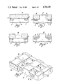
- FIGS. 1-16 show the work piece (structure) at various stages of its fabrication in accordance with the invention of which FIG. 5 is a perspective plan view and the remaining figures are sectional views.
- FIG. 4 is shown along the line 4--4 of FIG. 5. The remaining views are shown along the same plane but in other stages of manufacture.
- FIG. 1 there is shown a cross-sectional view of a semiconductor body 10 having a surface 12 on which a relatively thick insulator layer 14 is formed.
- Semiconductor body 10 is typically monocrystalline silicon having a high resistivity and having a dopant concentration of about 1 ⁇ 10 15 atoms/per cubic centimeter.
- Body 10 may be of p or n type conductivity. In the specific example being described, it will be assumed that the doping of body 10 is p-type, as is characteristic of the more widely used n-channel MOS transistor, and that it is formed from (100) single crystal silicon.
- Insulator layer 14 Before insulator layer 14 is formed, body 10 is masked and an ion implant of p-type impurities is selectively done so as to heavily dope (to approximately 1 ⁇ 10 18 to 1 ⁇ 10 19 atoms/per cubic centimeter) the portions 11 of body 10. This implant is used to increase the electrical isolation between transistors by preventing inversion of the implanted portions of body 10 as is known in the art. This is typically denoted as a field or channel stop implant.
- Insulator layer 14 is typically silicon dioxide which is typically 0.6 to 1.0 micron thick and may be thermally grown or deposited.
- surface 12 is planar and there will be formed hundreds or thousands or ten thousands of transistors and other devices. For the sake of convenience there will be illustrated the fabrication of a single transistor.
- FIG. 2 there is shown a hole (typically about 0.5 micron wide) through silicon dioxide layer 14 to surface 12 of silicon body 10.
- the width of this hole (the dimension in the plane of the paper) will determine the length of the channel (the separation between source and drain) of the transistor, so it is chosen appropriately.
- the dimension of the hole normal to the plane of the paper will control the maximum width of the channel, (the direction normal to the flow of carriers in the channel).
- This hole through silicon dioxide layer 14 is typically formed using well known photolithography masking techniques and anisotropic or trench etching techniques.
- the hole in dioxide layer 14 is shown as having been filled with silicon so as to form a finger-like member 16 which advantageously extends to be essentially flush with or slightly below the top surface of silicon dioxide layer 14.
- a selective epitaxial deposition of silicon which extends the single crystal silicon body up into the hole but does not deposit silicon firmly on exposed oxide surfaces, is used to form finger member 16. If necessary it is feasible to improve the crystalline nature by subsequent laser treatment as is known in the art.
- FIG. 4 is a perspective view of part of an array of the FIG. 4 type of structures after this etching step is completed. It shows a portion of finger element 16 exposed along its sides in recesses in the surrounding oxide layer 14, as shown without background lines in FIG. 4.
- FIG. 6 there is shown a conformal layer of silicon nitride 20 covering the entire exposed surfaces of finger member 16 and silicon dioxide layer 14.
- Layer 20 is typically deposited using well known chemical vapour deposition (CVD) techniques.
- Conformal silicon nitride 20 layer is then etched in an anisotropic nitride etch so as to leave only the two curved portions of silicon nitride 20a and 20b butting up against the sidewalls of finger 16, as seen in FIG. 7.
- anisotropic nitride etch is chosen to favor etching in the vertical direction as known in the art to achieve the result shown.
- silicon dioxide is formed over the entire top of the resulting structure, typically by exposing the structure to a moderately high oxidizing temperature of approximately 950° C., for a sufficient time.
- This oxidation step grows oxide at different rates on silicon, silicon oxide, and silicon nitride so that different thickness layers of silicon dioxide will be grown on the exposed silicon, silicon nitride, and existing oxide.
- the exposed silicon oxidizes most rapidly and a relatively thicker layer 22 of silicon dioxide is formed over the silicon, as compared to the layer 23 over the nitride.
- the existing thick oxide layer 14 increases in thickness inconsequentially. The resultant is shown in FIG. 8.
- a short isotropic oxide etch is used to remove all of the silicon dioxide layer 23 leaving a portion of layer 22 over the top of the finger.
- a selective silicon nitride etch is then used to remove the nitride sidewall portions 20a and 20b. This leaves the top of finger 16, lower portions and the end portions of the opposed vertical sidewalls of finger 16, and semiconductor body 10 covered by silicon dioxide. The only exposed silicon is at the upper intermediate portions of the opposed vertical sidewalls of finger 16. The resultant is shown in FIG. 9.
- a lateral selective epitaxial silicon growth step is then performed to grow silicon substantially epitaxially only in the exposed areas of silicon. Silicon deposited elsewhere can readily be selectively removed. The regions of laterally grown silicon are shown as 16a and 16b in FIG. 10, on opposed sides of the upmost portion of silicon finger 16. Although high quality monocrystalline silicon is not required for such regions, if desired, the crystallinity can be improved by known laser techniques.
- the layer of silicon dioxide 22 covering the top of finger 16 is then etched away to leave the structure of FIG. 11.
- This structure is clearly useful for the fabrication of insulated gate field effect transistors (IGFETs) in a variety of ways.
- an oxide suitable for use as the gate 26 oxide over the exposed surface of the silicon protruding from the surrounding silicon dioxide corresponding to the tops of finger 16 and regions 16a and 16b.
- the structure is optionally implanted with appropriate ions to adjust the threshold voltage of the transistor in a known fashion, if such adjustment is desired.
- a blanket layer of polycrystalline silicon suitable for use as the gate region (electrode) of the transistor is deposited over the top surface of the structure. After the blanket layer of polycrystalline silicon is deposited, the entire layer is doped heavily n-type (1 ⁇ 10 20 atoms per cubic centimeter), such as from a phosphorus source at about 950° C. This layer is then patterned in the usual fashion to leave a portion, of the desired dimensions for the gate region (electrode) 28, over the central portion of the top surface, corresponding essentially to the original finger surface as is shown in FIG. 12.
- This structure is then heated again in an oxidizing ambient to lightly oxidize the exposed surfaces of polycrystalline portion 28, and form a protective layer 26a, before subjecting the structure in a known fashion to high dosage implants of donor ions to dope regions 16a and 16b not covered by polysilicon gate portion 28 heavily n-type, so that they can serve as source and drain regions, respectively, of the n-channel IGFET formed at the top of the finger 16.
- the dopant concentrations of both of regions 16a and 16b is approximately 1 ⁇ 10 18 to 1 ⁇ 10 19 atoms per cubic centimeter. It should be noted that there results a self-aligned gate structure, as is generally desired.
- the interface of the source and drain regions with the silicon is essentially limited to the channel portion of the transistor, thereby to achieve the low parasitic capacitance desired.
- the remainders of regions 16a and 16b are bounded by dielectric material (typically silicon dioxide). It is characteristic of the resulting transistor that its channel portion, which desirably should be of high quality monocrystalline silicon, was formed from material initially grown within the hole surrounded by silicon dioxide.
- a variety of techniques are available for this purpose.
- a preferred technique involves initially removing the thin thermally grown oxide layer which remains over the top surface of the structure and then depositing a relatively thick conformal layer 30 of silicon dioxide by chemical vapor deposition over the entire top surface of the structure, as shown in FIG. 13.
- an anisotropic oxide etch leaves in place of the conformal layer 30 only the spacer portions 30a which are positioned along the sidewalls of the polycrystalline gate region (electrode) 28 and their junctions with the regions 16a and 16b as shown in FIG. 14.
- the resultant is then covered with a refractory metal, typically tungsten, titanium or tantalum, and then subjected to a rapid thermal anneal to convert the metal in contact with the silicon to a silicide but to leave unreacted the metal over the sidewall spacers 30a and 30b.
- This anneal also can serve to activate the ions earlier implanted into regions 16a and 16b.
- the unreacted metal can then be easily removed by a selective etch which little affects the silicide.
- the resultant is shown in FIG. 15 where a first part of the silicide layer 32c covers the top of the gate region 28, a second part of the silicide layer 32a covers surface portions of region 16a, and a third part of the silicide layer 32b cover surface portions of region 16b.
- a phosphorus-rich glass layer 34 is deposited over the top surface of the structure and openings are formed in it wherever electrical contact is to be made to the transistor, i.e., the source, drain and gate regions. Standard techniques are available for this purpose.
- a layer of the contact metal typically an aluminum-silicon alloy, is deposited over the glass to fill the via openings and this layer is patterned to provide the desired interconnection pattern between the transistors and any other devices (not shown) formed on or in body 10 as needed for an integrated circuit.
- FIG. 16 where the glass layer 34 is shown provided with openings filled with the aluminum-silicon alloy to contact the silicide portions 32a, 32b, and 32c over the source region 16a, the drain region 16b, and the gate region 28, respectively.
- the aluminum-silicide alloy contacts to silicide regions 32a, 32b, and 32c are shown as 36a, 36b, and 36c, respectively. In some instances, two levels of metalization may be needed.
- SOIL Silicon-On-Insulator-Like
- the advantages of a SOIL IGFET compared to a conventional IGFET are: 1. a reduction in the n-type drain and source to the p-type substrate area which means a reduction in parasitic capacitance, that increase radiation hardness and reduces leakage currents; 2. reduced isolation spacing between devices which increases packing density; 3. a reduction in spurious metal to substrate shorts; and 4. easier substrate biasing to eliminate "kink effects”.
- the SOIL device of the present invention is also easier to fabricate than other known SOIL devices.
- the semiconductor body can be gallium arsenide and ternary and quaternary compounds of III-V compounds such as InGaAs and AlGaInP with the process modified to be consistent with the processing requirements of these materials.
- the structure could comprise GaAs grown on a CVD layer of SiN.
- the hole in silicon dioxide layer 14 need not be completely filled with grown silicon.
Abstract
Description
Claims (9)
Priority Applications (1)
| Application Number | Priority Date | Filing Date | Title |
|---|---|---|---|
| US06/940,255 US4716128A (en) | 1986-12-10 | 1986-12-10 | Method of fabricating silicon-on-insulator like devices |
Applications Claiming Priority (1)
| Application Number | Priority Date | Filing Date | Title |
|---|---|---|---|
| US06/940,255 US4716128A (en) | 1986-12-10 | 1986-12-10 | Method of fabricating silicon-on-insulator like devices |
Publications (1)
| Publication Number | Publication Date |
|---|---|
| US4716128A true US4716128A (en) | 1987-12-29 |
Family
ID=25474507
Family Applications (1)
| Application Number | Title | Priority Date | Filing Date |
|---|---|---|---|
| US06/940,255 Expired - Fee Related US4716128A (en) | 1986-12-10 | 1986-12-10 | Method of fabricating silicon-on-insulator like devices |
Country Status (1)
| Country | Link |
|---|---|
| US (1) | US4716128A (en) |
Cited By (13)
| Publication number | Priority date | Publication date | Assignee | Title |
|---|---|---|---|---|
| US5023197A (en) * | 1989-08-16 | 1991-06-11 | French State Represented By The Minister Of Post, Telecommunications And Space | Manufacturing process of mesa SOI MOS transistor |
| US5061644A (en) * | 1988-12-22 | 1991-10-29 | Honeywell Inc. | Method for fabricating self-aligned semiconductor devices |
| EP0480373A2 (en) * | 1990-10-09 | 1992-04-15 | Seiko Epson Corporation | Thin-film semiconductor device |
| US5146304A (en) * | 1988-12-22 | 1992-09-08 | Honeywell Inc. | Self-aligned semiconductor device |
| US5340754A (en) * | 1992-09-02 | 1994-08-23 | Motorla, Inc. | Method for forming a transistor having a dynamic connection between a substrate and a channel region |
| US5597738A (en) * | 1993-12-03 | 1997-01-28 | Kulite Semiconductor Products, Inc. | Method for forming isolated CMOS structures on SOI structures |
| US6017801A (en) * | 1997-09-24 | 2000-01-25 | Lg Semicon Co., Ltd. | Method for fabricating field effect transistor |
| US6091123A (en) * | 1998-06-08 | 2000-07-18 | Advanced Micro Devices | Self-aligned SOI device with body contact and NiSi2 gate |
| SG85156A1 (en) * | 1999-01-28 | 2001-12-19 | Ibm | Method of integrating substrate contact on soi wafers with sti process |
| US20020153612A1 (en) * | 1998-08-19 | 2002-10-24 | Salman Akram | Silicide pattern structures and methods of fabricating the same |
| US20050093074A1 (en) * | 2003-11-05 | 2005-05-05 | International Business Machines Corporation | Method of fabricating a finfet |
| US20070026617A1 (en) * | 2000-10-18 | 2007-02-01 | Adkisson James W | Method of fabricating semiconductor side wall fin |
| US20100001318A1 (en) * | 2008-07-02 | 2010-01-07 | Nec Electronics Corporation | Field effect transistor, method of manufacturing the same, and semiconductor device |
Citations (7)
| Publication number | Priority date | Publication date | Assignee | Title |
|---|---|---|---|---|
| EP0042552A2 (en) * | 1980-06-16 | 1981-12-30 | Kabushiki Kaisha Toshiba | MOS type semiconductor device |
| US4402761A (en) * | 1978-12-15 | 1983-09-06 | Raytheon Company | Method of making self-aligned gate MOS device having small channel lengths |
| US4404732A (en) * | 1981-12-07 | 1983-09-20 | Ibm Corporation | Self-aligned extended epitaxy mesfet fabrication process |
| US4419811A (en) * | 1982-04-26 | 1983-12-13 | Acrian, Inc. | Method of fabricating mesa MOSFET using overhang mask |
| US4494304A (en) * | 1983-03-04 | 1985-01-22 | Oki Electric Industry Co., Ltd. | Forming chan-stops by selectively implanting impurity ions through field-oxide layer during later stage of MOS-device fabrication |
| US4523213A (en) * | 1979-05-08 | 1985-06-11 | Vlsi Technology Research Association | MOS Semiconductor device and method of manufacturing the same |
| US4530149A (en) * | 1982-06-24 | 1985-07-23 | Rca Corporation | Method for fabricating a self-aligned vertical IGFET |
-
1986
- 1986-12-10 US US06/940,255 patent/US4716128A/en not_active Expired - Fee Related
Patent Citations (7)
| Publication number | Priority date | Publication date | Assignee | Title |
|---|---|---|---|---|
| US4402761A (en) * | 1978-12-15 | 1983-09-06 | Raytheon Company | Method of making self-aligned gate MOS device having small channel lengths |
| US4523213A (en) * | 1979-05-08 | 1985-06-11 | Vlsi Technology Research Association | MOS Semiconductor device and method of manufacturing the same |
| EP0042552A2 (en) * | 1980-06-16 | 1981-12-30 | Kabushiki Kaisha Toshiba | MOS type semiconductor device |
| US4404732A (en) * | 1981-12-07 | 1983-09-20 | Ibm Corporation | Self-aligned extended epitaxy mesfet fabrication process |
| US4419811A (en) * | 1982-04-26 | 1983-12-13 | Acrian, Inc. | Method of fabricating mesa MOSFET using overhang mask |
| US4530149A (en) * | 1982-06-24 | 1985-07-23 | Rca Corporation | Method for fabricating a self-aligned vertical IGFET |
| US4494304A (en) * | 1983-03-04 | 1985-01-22 | Oki Electric Industry Co., Ltd. | Forming chan-stops by selectively implanting impurity ions through field-oxide layer during later stage of MOS-device fabrication |
Non-Patent Citations (10)
| Title |
|---|
| "A Bird's Beak Free Local Oxidation Technology Feasible for VSLI Circuits Fabrication," Kuang Yi Chiu et al., IEEE Transactions on Electron Devices, vol. ED-29, No. 4, Apr. 1982, pp. 536-540. |
| "Alternatives to LOCOS Could Aid Isolation Technology," Semiconductor International, Mar. 1984, pp. 19 and 20. |
| "Development of the Self-Aligned Titanium Silicide Process for VLSI Applications," Michael E. Alperin et al., IEEE Journal of Solid-State Circuits, vol. SC-20, No. 1, Feb. 1985, pp. 61-69. |
| "Selective Low-Pressure Silicon Epitaxy for MOS and Bipolar Transistor Application," Hans Kurten et al., IEEE Transactions on Electron Devices, vol. ED-30, No. 11, Nov. 1983, pp. 1511-1515. |
| "The Sloped-Wall SWAMI--A Defect-Free Zero Bird's-Beak Local Oxidation Process for Scaled VLSI Technology," Kuang Y. Chiu et al., IEEE Transactions on Electron Devices, vol. ED-30, No. 11, Nov. 1983, pp. 1506-1511. |
| A Bird s Beak Free Local Oxidation Technology Feasible for VSLI Circuits Fabrication, Kuang Yi Chiu et al., IEEE Transactions on Electron Devices, vol. ED 29, No. 4, Apr. 1982, pp. 536 540. * |
| Alternatives to LOCOS Could Aid Isolation Technology, Semiconductor International, Mar. 1984, pp. 19 and 20. * |
| Development of the Self Aligned Titanium Silicide Process for VLSI Applications, Michael E. Alperin et al., IEEE Journal of Solid State Circuits, vol. SC 20, No. 1, Feb. 1985, pp. 61 69. * |
| Selective Low Pressure Silicon Epitaxy for MOS and Bipolar Transistor Application, Hans Kurten et al., IEEE Transactions on Electron Devices, vol. ED 30, No. 11, Nov. 1983, pp. 1511 1515. * |
| The Sloped Wall SWAMI A Defect Free Zero Bird s Beak Local Oxidation Process for Scaled VLSI Technology, Kuang Y. Chiu et al., IEEE Transactions on Electron Devices, vol. ED 30, No. 11, Nov. 1983, pp. 1506 1511. * |
Cited By (29)
| Publication number | Priority date | Publication date | Assignee | Title |
|---|---|---|---|---|
| US5061644A (en) * | 1988-12-22 | 1991-10-29 | Honeywell Inc. | Method for fabricating self-aligned semiconductor devices |
| US5146304A (en) * | 1988-12-22 | 1992-09-08 | Honeywell Inc. | Self-aligned semiconductor device |
| US5023197A (en) * | 1989-08-16 | 1991-06-11 | French State Represented By The Minister Of Post, Telecommunications And Space | Manufacturing process of mesa SOI MOS transistor |
| EP0480373A2 (en) * | 1990-10-09 | 1992-04-15 | Seiko Epson Corporation | Thin-film semiconductor device |
| EP0480373A3 (en) * | 1990-10-09 | 1993-03-10 | Seiko Epson Corporation | Thin-film semiconductor device |
| US5294821A (en) * | 1990-10-09 | 1994-03-15 | Seiko Epson Corporation | Thin-film SOI semiconductor device having heavily doped diffusion regions beneath the channels of transistors |
| US5340754A (en) * | 1992-09-02 | 1994-08-23 | Motorla, Inc. | Method for forming a transistor having a dynamic connection between a substrate and a channel region |
| US5393681A (en) * | 1992-09-02 | 1995-02-28 | Motorola, Inc. | Method for forming a compact transistor structure |
| US5527723A (en) * | 1992-09-02 | 1996-06-18 | Motorola, Inc. | Method for forming a dynamic contact which can be either on or off or switched therebetween |
| US5627395A (en) * | 1992-09-02 | 1997-05-06 | Motorola Inc. | Vertical transistor structure |
| US5597738A (en) * | 1993-12-03 | 1997-01-28 | Kulite Semiconductor Products, Inc. | Method for forming isolated CMOS structures on SOI structures |
| US6017801A (en) * | 1997-09-24 | 2000-01-25 | Lg Semicon Co., Ltd. | Method for fabricating field effect transistor |
| US6372563B1 (en) | 1998-06-08 | 2002-04-16 | Advanced Micro Devices, Inc. | Self-aligned SOI device with body contact and NiSi2 gate |
| US6091123A (en) * | 1998-06-08 | 2000-07-18 | Advanced Micro Devices | Self-aligned SOI device with body contact and NiSi2 gate |
| US20050136647A1 (en) * | 1998-08-19 | 2005-06-23 | Salman Akram | Methods of fabricating contact interfaces |
| US20020153612A1 (en) * | 1998-08-19 | 2002-10-24 | Salman Akram | Silicide pattern structures and methods of fabricating the same |
| US6599832B2 (en) * | 1998-08-19 | 2003-07-29 | Micron Technology, Inc. | Silicide pattern structures and methods of fabricating the same |
| US20040038511A1 (en) * | 1998-08-19 | 2004-02-26 | Salman Akram | Methods of fabricating silicide pattern structures |
| US6716745B2 (en) | 1998-08-19 | 2004-04-06 | Micron Technology, Iinc. | Silicide pattern structures and methods of fabricating the same |
| US6881663B2 (en) | 1998-08-19 | 2005-04-19 | Micron Technology, Inc. | Methods of fabricating silicide pattern structures |
| US6521947B1 (en) | 1999-01-28 | 2003-02-18 | International Business Machines Corporation | Method of integrating substrate contact on SOI wafers with STI process |
| SG85156A1 (en) * | 1999-01-28 | 2001-12-19 | Ibm | Method of integrating substrate contact on soi wafers with sti process |
| US7265417B2 (en) | 2000-10-18 | 2007-09-04 | International Business Machines Corporation | Method of fabricating semiconductor side wall fin |
| US20070026617A1 (en) * | 2000-10-18 | 2007-02-01 | Adkisson James W | Method of fabricating semiconductor side wall fin |
| US7361556B2 (en) | 2000-10-18 | 2008-04-22 | International Business Machines Corporation | Method of fabricating semiconductor side wall fin |
| US6962843B2 (en) | 2003-11-05 | 2005-11-08 | International Business Machines Corporation | Method of fabricating a finfet |
| US20050093074A1 (en) * | 2003-11-05 | 2005-05-05 | International Business Machines Corporation | Method of fabricating a finfet |
| US20100001318A1 (en) * | 2008-07-02 | 2010-01-07 | Nec Electronics Corporation | Field effect transistor, method of manufacturing the same, and semiconductor device |
| US8587027B2 (en) * | 2008-07-02 | 2013-11-19 | Renesas Electronics Corporation | Field effect transistor, method of manufacturing the same, and semiconductor device |
Similar Documents
| Publication | Publication Date | Title |
|---|---|---|
| US4503601A (en) | Oxide trench structure for polysilicon gates and interconnects | |
| US4948745A (en) | Process for elevated source/drain field effect structure | |
| EP0139371B1 (en) | Process for manufacturing a mos integrated circuit employing a method of forming refractory metal silicide areas | |
| US4808548A (en) | Method of making bipolar and MOS devices on same integrated circuit substrate | |
| US6048756A (en) | Method for making a silicon-on-insulator MOS transistor using a selective SiGe epitaxy | |
| KR100905210B1 (en) | CMOS vertical replacement gate VRG transistors | |
| US7045409B2 (en) | Semiconductor device having active regions connected together by interconnect layer and method of manufacture thereof | |
| EP0480635B1 (en) | Thin film transistor and a method of manufacturing thereof | |
| US5371026A (en) | Method for fabricating paired MOS transistors having a current-gain differential | |
| US4521448A (en) | Method of manufacturing semiconductor device | |
| US4749441A (en) | Semiconductor mushroom structure fabrication | |
| US5118639A (en) | Process for the formation of elevated source and drain structures in a semiconductor device | |
| US6709935B1 (en) | Method of locally forming a silicon/geranium channel layer | |
| US4855246A (en) | Fabrication of a gaas short channel lightly doped drain mesfet | |
| US20070018236A1 (en) | Semiconductor device and manufacturing method thereof | |
| JP2000277745A (en) | Double-gate integrated circuit and manufacture of the same | |
| US4486266A (en) | Integrated circuit method | |
| JPH09172173A (en) | Semiconductor device and its manufacture | |
| US4716128A (en) | Method of fabricating silicon-on-insulator like devices | |
| US20020009859A1 (en) | Method for making SOI MOSFET | |
| US5932913A (en) | MOS transistor with controlled shallow source/drain junction, source/drain strap portions, and source/drain electrodes on field insulation layers | |
| US4714685A (en) | Method of fabricating self-aligned silicon-on-insulator like devices | |
| US6724049B2 (en) | SOI semiconductor device with insulating film having different properties relative to the buried insulating film | |
| US6593175B2 (en) | Method of controlling a shape of an oxide layer formed on a substrate | |
| US6190179B1 (en) | Method of making a field effect transistor having a channel in an epitaxial silicon layer |
Legal Events
| Date | Code | Title | Description |
|---|---|---|---|
| AS | Assignment |
Owner name: GENERAL MOTORS CORPORATION, DETROIT, MICHIGAN, A C Free format text: ASSIGNMENT OF ASSIGNORS INTEREST.;ASSIGNORS:SCHUBERT, PETER J.;ALVI, NADEEM S.;REEL/FRAME:004651/0993;SIGNING DATES FROM 19861117 TO 19861118 Owner name: GENERAL MOTORS CORPORATION, MICHIGAN Free format text: ASSIGNMENT OF ASSIGNORS INTEREST;ASSIGNORS:SCHUBERT, PETER J.;ALVI, NADEEM S.;SIGNING DATES FROM 19861117 TO 19861118;REEL/FRAME:004651/0993 |
|
| REMI | Maintenance fee reminder mailed | ||
| LAPS | Lapse for failure to pay maintenance fees | ||
| FP | Expired due to failure to pay maintenance fee |
Effective date: 19911229 |
|
| STCH | Information on status: patent discontinuation |
Free format text: PATENT EXPIRED DUE TO NONPAYMENT OF MAINTENANCE FEES UNDER 37 CFR 1.362 |