US4708677A - Method of measuring the temperature of a photocathode - Google Patents
Method of measuring the temperature of a photocathode Download PDFInfo
- Publication number
- US4708677A US4708677A US06/814,148 US81414885A US4708677A US 4708677 A US4708677 A US 4708677A US 81414885 A US81414885 A US 81414885A US 4708677 A US4708677 A US 4708677A
- Authority
- US
- United States
- Prior art keywords
- temperature
- layer
- thickness
- wafer
- apparent
- Prior art date
- Legal status (The legal status is an assumption and is not a legal conclusion. Google has not performed a legal analysis and makes no representation as to the accuracy of the status listed.)
- Expired - Lifetime
Links
Images


Classifications
-
- H—ELECTRICITY
- H01—ELECTRIC ELEMENTS
- H01J—ELECTRIC DISCHARGE TUBES OR DISCHARGE LAMPS
- H01J9/00—Apparatus or processes specially adapted for the manufacture, installation, removal, maintenance of electric discharge tubes, discharge lamps, or parts thereof; Recovery of material from discharge tubes or lamps
- H01J9/02—Manufacture of electrodes or electrode systems
- H01J9/12—Manufacture of electrodes or electrode systems of photo-emissive cathodes; of secondary-emission electrodes
Definitions
- This invention relates to image intensifier tubes and more particularly to photoemissive cathodes for use in such tubes.
- Image intensifier tubes multiply the amount of incident light they receive and thus provide an increase in light output which can be supplied either to a camera or directly to the eyes of a viewer. These devices are particularly useful for providing images from dark regions and have both industrial and military application. For example, these devices are used for enhancing the night vision of aviators, for photographing extraterrestrial bodies and for providing night vision to sufferers of retinitis pigmentosa (night blindness).
- Image intensifier tubes utilize a photoemissive wafer which is bonded to a glass faceplate to form a cathode. Light enters the faceplate and strikes the wafer, thereby causing a primary emission of electrons.
- a heat cleaning step is performed to remove contaminants, such as oxygen and carbon from the surface of the photoemissive wafer. Bringing the cathode to a specific temperature and maintaining the cathode at that temperature are necessary in effecting proper heat cleaning of the cathode so that its structure and properties are not adversely affected. Knowing the heat cleaning temperature is also necessary in order to avoid the formation of brush lines in the otherwise transparent photoemissive wafer.
- Thermocouples cannot be used to measure the temperature of cathodes because they tend to damage the fragile surface of the cathode or give inaccurate readings.
- the most convenient method is radiative measurement of the temperature using a thermometer based on detection of blackbody radiation.
- Instruments which detect infrared radiation a wavelengths for which the layers are transparent and the glass is opaque sense the radiation from a thin layer at the interface of the glass and wafer plus a contribution from the wafer. Due to the proximity of the interface to the gallium arsenide layer and the good thermal conductivity of semiconductors, the measured temperature is a good indicator of the true wafer temperature. However, the wafer acts as a thin film which causes the apparent temperature to vary by a large amount due to interference effects caused by multiple reflection of the blackbody radiation between the internal surfaces of the wafer. However, by measuring the thickness of the wafer and knowing the indices of refraction, a correction can be made for the interference.
- the present invention provides a method of determining the temperature of a layered structure which includes at least one layer of an infrared transparent material including measuring the thickness of the material, determining the level of radiation being emitted or transmitted through by the layered structure, applying a correction factor derived from the thickness measurement and calculating the temperature of the structure from the correction factor and the radiation level.
- FIG. 1 is a cross-sectional view of a cathode usable in an image intensifier tube in accordance with this invention
- FIG. 2 is a cross-sectional view of the photoemissive wafer prior to bonding
- FIG. 3 is a diagrammatic representation of the temperature measuring apparatus of this invention.
- FIG. 4 is the correction factor curve in accordance with the invention.
- FIG. 5 is a graph of an interference pattern.
- FIG. 1 there is shown a cathode 10 which includes a faceplate 12 and a photoemissive wafer 14.
- the faceplate 12 can be made of a clear, high quality optical glass such as Corning 7056. This glass comprises 70 percent silica (SiO 2 ), 17 percent boric oxide (B 2 O 3 ), 8 percent potash (K 2 O), 3 percent alumina (Al 2 O 3 ) and 1 percent each of soda (Na 2 O) and lithium oxide (Li 2 O). Other glasses may, of course, be used.
- the faceplate 12 includes a central, generally circular body portion 12a and a reduced thickness sill portion 12b in the form of a flange surrounding the body portion.
- One surface 34 of the faceplate 12 extends continuously across the body and sill portions 12a and 12b, respectively, and the portion of this surface extending over the sill portion 12b and a small adjacent portion of the central body portion 12a fits under a flange 36 and is secured thereto to retain the faceplate 12 in a housing (not shown).
- the remainder of the portion of surface 34, that is, that portion surrounded by the flange 36 is the exposed surface of the faceplate 12 on which input light impinges.
- the faceplate 12 also includes surface portions 38a and 38b which are generally parallel to surface 34 and which extend over the body portion 12a and sill portion 12b, respectively. Because of the difference in thickness between the body portion 12a and the sill portion 12b, the surface portions 38a and 38b lie in different planes with the portion 38a being spaced farther from the surface 34 than is the portion 38b. Extending between the surface portions 38a and 38b is a connecting surface portion 38c which, in the embodiment disclosed herein, is generally frusto-conical.
- the photoemissive wafer 14 is bonded to the surface portion 38a so that light impinging on the exposed portion of surface 34 and eventually striking the wafer 14 causes the emission of electrons. These electrons are accelerated across a gap by an electric field to a MCP 40 causing the secondary emission of electrons all in accordance with known principles.
- Connecting the photoemissive wafer 14 to an external biasing power supply is a coating of conductive material 42 applied to the surfaces 16b and 16c and also over a portion of surface 16a so that this coating makes contact with the wafer 14.
- the photoemissive wafer 14 may be formed in any known manner. One such method is described with reference to FIG. 2.
- a gallium arsenide (GaAs) substrate 16 has formed on one of its surfaces a layer 18 of gallium arsenide (GaAs) which is identified as a buffer layer. The formation of the buffer layer 18 is to facilitate control of a later etching process to remove the substrate.
- An etch stop layer 20 of gallium aluminum arsenide (GaAlAs) is formed on top of the buffer layer 18 and an active layer 22 of gallium arsenide (GaAs) is formed on the etch stop layer 20.
- the active layer 22 has a layer of gallium aluminum arsenide (GaAlAs) formed on its surface and is identified as the window layer 24.
- GaAlAs gallium aluminum arsenide
- formation of the wafer 14 results in a structure which is larger than that required for the image intensifier tube.
- One way of achieving the proper diameter for the wafer 14 is to cut the wafer with a saw. If this step is to be performed, then cap layer 26 of gallium arsenide (GaAs) is formed on top of the window layer 24. This cap layer 26 will provide protection to the underlying structure during cutting to prevent chipping of the window layer 24.
- Another way of achieving the proper wafer diameter is to carefully chip away the excess portions of the wafer 14 after it is bonded to the glass faceplate 12. In using this method, a cap layer is not necessary.
- each of the layers is by means of epitaxial growth.
- cap layer 26 is used, it is removed after cutting, preferably by chemical means such as etching.
- a thin layer 28 of silicon nitride (Si 3 N 4 ).
- the silicon nitride layer 28 has a layer 30 of silicon dioxide (SiO 2 ) deposited on its surface. Both the silicon nitride layer 28 and the silicon dioxide layer 30 are preferably formed by sputter deposition. The structure so formed is identified as a wafer 32.
- the wafer 32 is positioned with the silicon dioxide layer 30 against the surface portion 38a of the faceplate 12.
- the wafer 32 is bonded to the faceplate 12 in a bonding apparatus to form a unitary structure.
- the temperature in the bonding apparatus is raised and pressure is applied to the wafer 32 and the faceplate 12 for a length of time sufficient for bonding to occur and for a unitary structure to be formed. After bonding, the unitary structure is cooled.
- the GaAs substrate 16 removed. This is preferably done by lapping off most of the substrate 16 by mechanical polishing. The remaining portion of the substrate 16 is thereafter removed by chemical etching. The buffer layer 18 and the etch stop layer 20 are also removed, preferably by a chemical etching process. The structure is now identified as the cathode 10.
- the conductive coatings 42 are applied to the surface portions 38b and 38c and a small portion of 38a which is contiguous with 38c.
- the cathode 10 is then heat cleaned to remove contaminants from the surface of the wafer 14.
- the heat cleaning temperature is dependent upon the nature of the contaminants and upon the nature of the surface from which the contaminants are to be removed; that is, the actual percentage of gallium and arsenic at the surface. Once the nature of the contaminants and the actual ratio of gallium to arsenic is known, a specific heat cleaning temperature is determined. A temperature of approximately 600° C. is sufficient to free contaminants such as oxygen and carbon where the ratio of gallium to arsenic is 1:1.
- the cathode 10 is placed in a high vacuum chamber 50 and is heated to the predetermined temperature.
- a pyrometer 54 receives radiation emitted by the cathode 12 through a window 56 in the chamber 50. At the predetermined temperature contaminants are freed from the cathode 10 and are removed by the vacuum system. Heat is provided by means of a lamp 52, although any other suitable heat source may be used.
- the embodiment of the invention uses a predetermined temperature of approximately 600° C.
- Another problem which is related to the heat cleaning temperature is the appearance of brush lines or crosshatching marks which result from stresses arising between the GaAs substrate 14 and the glass faceplate 12 during the cooling stage following bonding or heat cleaning.
- the lines or marks appear at a point within the range of temperatures used for heat cleaning. Therefore, it is important to maintain the heat cleaning temperature below that point.
- Methods of measuring the temperature of the cathode include measurement of the peak wavelength being emitted by the cathode. Since the body emits an envelope of wavelengths, it is also possible to measure the intensity of any wavelength in the envelope.
- One instrument used to measure wavelengths in a specific range is a pyrometer which uses black body radiation to measure the peak wavelength being emitted by a body and translating that wavelength into temperature.
- the particular type of pyrometer used herein is an IRCON with an operating range of 4.8-5.2 ⁇ m.
- the wafer 14 is very thin and it is difficult to monitor the blackbody radiation of such a thin layer, except if one chose to look only at a short wavelength whose absorption length is a small fraction of the cathode thickness (e.g. ⁇ 0.6 ⁇ m, where absorption length is less than 0.25 ⁇ m).
- This fundamental limitation is based on the relationship between the emittance and the absorbance.
- the transparency thickness and index of refraction of the wafer 14 cause light which enters one surface of the wafer 14 to be reflected one or more times before being transmitted through the other surface of the wafer.
- the result is a fringe pattern or fluctuation of energy and output with wavelengths which affect the pyrometer reading.
- a slight variation in thickness of the wafer 14 will affect the readings of the pyrometer since the interference phenomenon is very sensitive to thickness. Hence totally erroneous temperature readings will result from the spectral redistribution of energy caused by the interference.
- the wafer 14 may be considered to be a homogenous material. Therefore determining the thicknesses of the individual component layers of the wafer 14 is not necessary.
- the apparent temperature of several cathodes is measured using an IRCON pyrometer under carefully controlled conditions such as by enclosing the cathodes in a heated cavity of accurately known and constant temperature. Cathodes are used which have the same wafer thickness. After the IRCON readings are taken and the apparent temperatures found, the cathodes are removed from the cavity and are cooled. Each of the cathodes then has a thin layer of the wafer 14 removed, for example, by etching. The thickness of the layer which is removed is made exactly the same for each cathode. The cathodes are again enclosed in a heated cavity and IRCON readings taken. The cathodes are again removed from the cavity and cooled. These steps are performed a number of times. At each IRCON reading stage, the apparent temperatures of the cathodes are averaged and used to establish an apparent temperature which corresponds to the desired actual temperature.
- each of the wafers 14 is measured either before or after heating by nondestructive means and confirmed by destructive means, if needed.
- One method of performing the destructive measurement includes cutting a cross section of the wafer 14 and viewing the cut section under an electron microscope. A curve of apparent temperatures, corresponding to a desired actual temperature, versus thickness is thus generated. This curve is also known as a correction curve.
- the thickness is known, the apparent temperature which is needed to achieve the desired actual temperature is determined from the curve.
- One such method of measuring thickness consists of determining the fringe spacings in the infrared as the wave number is varied. This measurement can be done on a conventional infrared spectrophotometer or on a Fourier transform infrared instrument. The thickness is calculated from the fringe spacing and used to look up the correction factor on the previously generated compensation curve.
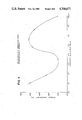
- FIG. 4 shows the correction factor for achieving an actual temperature of 600° C.
- a wafer having a thickness of 0.3 ⁇ m is raised to an apparent temperature of approximately 620° C. as determined from FIG. 4.
- Applying a correction factor based on the thickness of the material versus an apparent temperature to establish a predetermined actual temperature of the structure may also be accomplished by formulating a program which can be inserted into a computer.
- the correction factor has been determined, the heat being emitted by the heat source is adjusted to achieve the predetermined actual temperature.
- a typical interference curve is shown in FIG. 5.
Abstract
Description
Claims (5)
Priority Applications (1)
| Application Number | Priority Date | Filing Date | Title |
|---|---|---|---|
| US06/814,148 US4708677A (en) | 1985-12-27 | 1985-12-27 | Method of measuring the temperature of a photocathode |
Applications Claiming Priority (1)
| Application Number | Priority Date | Filing Date | Title |
|---|---|---|---|
| US06/814,148 US4708677A (en) | 1985-12-27 | 1985-12-27 | Method of measuring the temperature of a photocathode |
Publications (1)
| Publication Number | Publication Date |
|---|---|
| US4708677A true US4708677A (en) | 1987-11-24 |
Family
ID=25214303
Family Applications (1)
| Application Number | Title | Priority Date | Filing Date |
|---|---|---|---|
| US06/814,148 Expired - Lifetime US4708677A (en) | 1985-12-27 | 1985-12-27 | Method of measuring the temperature of a photocathode |
Country Status (1)
| Country | Link |
|---|---|
| US (1) | US4708677A (en) |
Cited By (8)
| Publication number | Priority date | Publication date | Assignee | Title |
|---|---|---|---|---|
| US4805187A (en) * | 1987-10-15 | 1989-02-14 | General Electric Company | Determination of substrate temperature used during oxygen implantation of SIMOX wafer |
| US4890933A (en) * | 1988-02-17 | 1990-01-02 | Itt Corporation | Transmission method to determine and control the temperature of wafers or thin layers with special application to semiconductors |
| US5098199A (en) * | 1988-02-17 | 1992-03-24 | Itt Corporation | Reflectance method to determine and control the temperature of thin layers or wafers and their surfaces with special application to semiconductors |
| US5114373A (en) * | 1991-02-11 | 1992-05-19 | Itt Corporation | Method for optimizing photo cathode photo-response |
| US5167452A (en) * | 1988-02-17 | 1992-12-01 | Itt Corporation | Transmission method to determine and control the temperature of wafers or thin layers with special application to semiconductors |
| US5170041A (en) * | 1988-02-17 | 1992-12-08 | Itt Corporation | Transmission method to determine and control the temperature of wafers or thin layers with special application to semiconductors |
| EP2073242A2 (en) | 2007-12-21 | 2009-06-24 | Siemens Aktiengesellschaft | Tube, especially electron tube |
| CN114927395A (en) * | 2022-04-24 | 2022-08-19 | 电子科技大学 | Method for controlling reflectivity of NEA GaN electron source in real time |
Citations (5)
| Publication number | Priority date | Publication date | Assignee | Title |
|---|---|---|---|---|
| US3245261A (en) * | 1961-11-07 | 1966-04-12 | Ici Ltd | Temperature measurement of plastic film |
| US3759102A (en) * | 1971-03-25 | 1973-09-18 | Steel Corp | Apparatus for determining correct pyrometer readings with steam interference present |
| US3793630A (en) * | 1971-06-14 | 1974-02-19 | Alnor Instr Co | Pyrometer with digitalized linearizing correction |
| JPS5393269A (en) * | 1977-01-27 | 1978-08-16 | Nec Corp | Automatic temperature compensation control equipment |
| US4418392A (en) * | 1980-06-26 | 1983-11-29 | Tokyo Shibaura Denki Kabushiki Kaisha | Measuring device |
-
1985
- 1985-12-27 US US06/814,148 patent/US4708677A/en not_active Expired - Lifetime
Patent Citations (5)
| Publication number | Priority date | Publication date | Assignee | Title |
|---|---|---|---|---|
| US3245261A (en) * | 1961-11-07 | 1966-04-12 | Ici Ltd | Temperature measurement of plastic film |
| US3759102A (en) * | 1971-03-25 | 1973-09-18 | Steel Corp | Apparatus for determining correct pyrometer readings with steam interference present |
| US3793630A (en) * | 1971-06-14 | 1974-02-19 | Alnor Instr Co | Pyrometer with digitalized linearizing correction |
| JPS5393269A (en) * | 1977-01-27 | 1978-08-16 | Nec Corp | Automatic temperature compensation control equipment |
| US4418392A (en) * | 1980-06-26 | 1983-11-29 | Tokyo Shibaura Denki Kabushiki Kaisha | Measuring device |
Cited By (11)
| Publication number | Priority date | Publication date | Assignee | Title |
|---|---|---|---|---|
| US4805187A (en) * | 1987-10-15 | 1989-02-14 | General Electric Company | Determination of substrate temperature used during oxygen implantation of SIMOX wafer |
| US4890933A (en) * | 1988-02-17 | 1990-01-02 | Itt Corporation | Transmission method to determine and control the temperature of wafers or thin layers with special application to semiconductors |
| US5098199A (en) * | 1988-02-17 | 1992-03-24 | Itt Corporation | Reflectance method to determine and control the temperature of thin layers or wafers and their surfaces with special application to semiconductors |
| US5167452A (en) * | 1988-02-17 | 1992-12-01 | Itt Corporation | Transmission method to determine and control the temperature of wafers or thin layers with special application to semiconductors |
| US5170041A (en) * | 1988-02-17 | 1992-12-08 | Itt Corporation | Transmission method to determine and control the temperature of wafers or thin layers with special application to semiconductors |
| US5114373A (en) * | 1991-02-11 | 1992-05-19 | Itt Corporation | Method for optimizing photo cathode photo-response |
| EP2073242A2 (en) | 2007-12-21 | 2009-06-24 | Siemens Aktiengesellschaft | Tube, especially electron tube |
| DE102007062054A1 (en) | 2007-12-21 | 2009-07-02 | Siemens Ag | Tube, in particular electron tube |
| US20090167133A1 (en) * | 2007-12-21 | 2009-07-02 | Oliver Heuermann | Electronic tube |
| CN114927395A (en) * | 2022-04-24 | 2022-08-19 | 电子科技大学 | Method for controlling reflectivity of NEA GaN electron source in real time |
| CN114927395B (en) * | 2022-04-24 | 2023-05-19 | 电子科技大学 | Method for controlling reflectivity of NEA GaN electron source in real time |
Similar Documents
| Publication | Publication Date | Title |
|---|---|---|
| US5568978A (en) | Optical apparatus and method for measuring temperature of a substrate material with a temperature dependent band gap | |
| KR100205156B1 (en) | Fabricating method of optoelectronic devices with gallium oxide coatings | |
| US4807994A (en) | Method of mapping ion implant dose uniformity | |
| CA2136886C (en) | Apparatus, system and method for real-time wafer temperature measurement based on light scattering | |
| US5317656A (en) | Fiber optic network for multi-point emissivity-compensated semiconductor wafer pyrometry | |
| US5229303A (en) | Device processing involving an optical interferometric thermometry using the change in refractive index to measure semiconductor wafer temperature | |
| US5156461A (en) | Multi-point pyrometry with real-time surface emissivity compensation | |
| US4352016A (en) | Method and apparatus for determining the quality of a semiconductor surface | |
| US5876119A (en) | In-situ substrate temperature measurement scheme in plasma reactor | |
| US5350236A (en) | Method for repeatable temperature measurement using surface reflectivity | |
| US6646752B2 (en) | Method and apparatus for measuring thickness of a thin oxide layer | |
| US4948937A (en) | Apparatus and method for heat cleaning semiconductor material | |
| US4708677A (en) | Method of measuring the temperature of a photocathode | |
| US5467732A (en) | Device processing involving an optical interferometric thermometry | |
| Kim et al. | Temperature dependence of the optical properties of CdTe | |
| Dumin | Measurement of film thickness using infrared interference | |
| US6174080B1 (en) | Apparatus and methods for measuring substrate temperature | |
| US5364187A (en) | System for repeatable temperature measurement using surface reflectivity | |
| EP0429081A2 (en) | Silicon wafer temperature measurement by optical transmission monitoring | |
| EP1043759B1 (en) | Method for processing silicon workpieces using hybrid optical thermometer system | |
| JP4166400B2 (en) | Radiation temperature measurement method | |
| US5624190A (en) | Method and apparatus for measuring the temperature of an object, in particular a semiconductor, by ellipsometry | |
| US5298831A (en) | Method of making photocathodes for image intensifier tubes | |
| US4533593A (en) | Antireflection coating for potassium chloride | |
| Jona et al. | Pyrometric Measurements of Si, Ge, and GaAs Wafers Between 100° and 700° C |
Legal Events
| Date | Code | Title | Description |
|---|---|---|---|
| AS | Assignment |
Owner name: ITT CORPORATION, 320 PARK AVENUE, NEW YORK, N.Y. 1 Free format text: ASSIGNMENT OF ASSIGNORS INTEREST.;ASSIGNORS:AMITH, AVRAHAM;BLANK, RICHARD E.;TIEN, ALBERT F.;REEL/FRAME:004524/0417 Effective date: 19860317 |
|
| FEPP | Fee payment procedure |
Free format text: PAYOR NUMBER ASSIGNED (ORIGINAL EVENT CODE: ASPN); ENTITY STATUS OF PATENT OWNER: LARGE ENTITY Free format text: PAYER NUMBER DE-ASSIGNED (ORIGINAL EVENT CODE: RMPN); ENTITY STATUS OF PATENT OWNER: LARGE ENTITY |
|
| STCF | Information on status: patent grant |
Free format text: PATENTED CASE |
|
| FPAY | Fee payment |
Year of fee payment: 4 |
|
| FEPP | Fee payment procedure |
Free format text: PAYER NUMBER DE-ASSIGNED (ORIGINAL EVENT CODE: RMPN); ENTITY STATUS OF PATENT OWNER: LARGE ENTITY Free format text: PAYOR NUMBER ASSIGNED (ORIGINAL EVENT CODE: ASPN); ENTITY STATUS OF PATENT OWNER: LARGE ENTITY |
|
| FPAY | Fee payment |
Year of fee payment: 8 |
|
| FPAY | Fee payment |
Year of fee payment: 12 |