US4692790A - Structure for connecting leadless chip carrier - Google Patents
Structure for connecting leadless chip carrier Download PDFInfo
- Publication number
- US4692790A US4692790A US06/772,342 US77234285A US4692790A US 4692790 A US4692790 A US 4692790A US 77234285 A US77234285 A US 77234285A US 4692790 A US4692790 A US 4692790A
- Authority
- US
- United States
- Prior art keywords
- support cover
- lcc
- frame
- chip carrier
- cover
- Prior art date
- Legal status (The legal status is an assumption and is not a legal conclusion. Google has not performed a legal analysis and makes no representation as to the accuracy of the status listed.)
- Expired - Lifetime
Links
Images


Classifications
-
- H—ELECTRICITY
- H05—ELECTRIC TECHNIQUES NOT OTHERWISE PROVIDED FOR
- H05K—PRINTED CIRCUITS; CASINGS OR CONSTRUCTIONAL DETAILS OF ELECTRIC APPARATUS; MANUFACTURE OF ASSEMBLAGES OF ELECTRICAL COMPONENTS
- H05K7/00—Constructional details common to different types of electric apparatus
- H05K7/02—Arrangements of circuit components or wiring on supporting structure
- H05K7/10—Plug-in assemblages of components, e.g. IC sockets
- H05K7/1053—Plug-in assemblages of components, e.g. IC sockets having interior leads
- H05K7/1061—Plug-in assemblages of components, e.g. IC sockets having interior leads co-operating by abutting
-
- H—ELECTRICITY
- H01—ELECTRIC ELEMENTS
- H01L—SEMICONDUCTOR DEVICES NOT COVERED BY CLASS H10
- H01L2924/00—Indexing scheme for arrangements or methods for connecting or disconnecting semiconductor or solid-state bodies as covered by H01L24/00
- H01L2924/0001—Technical content checked by a classifier
- H01L2924/0002—Not covered by any one of groups H01L24/00, H01L24/00 and H01L2224/00
Definitions
- the present invention relates to an improvement in a structure for accurately connecting a connection pattern provided on a leadless chip carrier (LCC) to that provided on a receiving surface using a connector in place of solder.
- LCC leadless chip carrier
- An LCC is usually provided with a connection pattern which is to be connected to that provided on a receiving surface, which is usually a printed circuit board, with the intermediary of a connector.
- a connection pattern which is to be connected to that provided on a receiving surface, which is usually a printed circuit board, with the intermediary of a connector.
- Such connection may be implemented with a structure in which a frame with a through bore is mounted on the receiving surface to surround the connection pattern on the receiving surface.
- the LCC is loosely received in the bore of the frame through a conductor connector, while a cover which has a pressing tongue at the center thereof presses the LCC from above to retain it in a predetermined position.
- the bore of the frame adapted to position the pattern on an LCC relative to the pattern on a receiving surface needs to be sized large enough to accommodate a product, or LCC, having the largest presumable dimensions. This, however, brings about a problem that when a relatively small LCC is placed in the relatively large bore of the frame, it is apt to move laterally or angularly inside the bore so that predetermined contacts of the pattern on the LCC fail to attain accurate contact with those of the pattern on the receiving surface, resulting in an imcomplete connection.
- the dimensional variations of LCCs extends over to the thickness for production reasons. Should such thicknesswise variations be left unabsorbed, the connector would fail to be constantly biased by an adequate force, constituting another cause of incomplete connection.
- the cover is provided with a pressing tongue which presses the LCC from above in order to absorb the thicknesswise variations.
- the tongue is provided with greater dimensions or a stronger biasing force.
- Such not only adds to the overall size and weight of the resulting package but also requires an LCC to be carefully designed in due consideration of its resistivity to externally derived pressures.
- the LCC has to be removed by turning the whole package and receiving surface upside down so that the LCC may drop out of the frame. It follows that where such a substrate is installed in an apparatus, the LCC cannot be removed unless the whole apparatus is turned upside down.
- a structure for connecting a first connection pattern provided on a leadless chip carrier (LCC) to a second connection pattern provided on a receiving surface of the present invention comprises a support cover for receiving and retaining the LCC therin and including a plurality of resilient portions for biasing the LCC inwardly from around the LCC, a frame for accommodating the support cover in the interior of the frame such that the first and second connecting patterns are connected to each other with the support cover, which has received the LCC, retained on the receiving surface, and a cover for pressing the support cover from above to retain the support cover and the LCC within the interior of the frame.
- a structure for accurately connecting a connection pattern on a leadless chip carrier to a connection pattern on a receiving surface by means of a connector i.e., without resorting to solder.
- the structure includes a generally frame- or box-shaped support cover in which the LCC is received.
- the support cover is provided with resilient portions at at least two sides of the inner contour thereof in order to resiliently hold the LCC therebetween.
- a frame surrounds the support cover to retain the same.
- the support cover in which the LCC is fit is coupled in the frame and retained therein by a pressure which is exerted by a cover
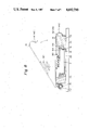
- FIG. 1 is an exploded perspective view of one possible structure for connecting an LCC
- FIG. 2 is an enlarged fragmentary view of a connector included in the structure of FIG. 1;
- FIG. 3 is a sectional side elevation showing the LCC of FIG. 1 in a packaged position
- FIG. 4 is a view representative of dislocation of a connection pattern on the LCC of FIG. 1 relative to that on a receiving surface;
- FIG. 5 is an exploded perspective view of an LCC connecting structure embodying the present invention.
- FIG. 6 is a section of the structure of FIG. 5 in which an LCC is packaged
- FIG. 7 is an exploded perspective view of another embodiment of the present invention.
- FIG. 8 is a section of the structure of FIG. 7 in which an LCC is packaged.
- FIGS. 1-4 an LCC connecting structure, shown in FIGS. 1-4, which has certain disadvantages overcome by the present invention.
- a receiving surface 10 is provided with a connection pattern 16 to face a connection pattern 14 provided on an LCC 12.
- the periphery of the pattern 16 is surrounded by a positioning frame 18.
- the LCC 12 is put in a through bore 20 of the frame 18 with the intermediary of a condutive connector 22 and, from above the LCC 12, a cover 24 with a pressing tongue 26 is pressed against the LCC 12 to fix it place.
- the frame 18 includes a pair of legs 28 and 30 and a pair of lugs or projections 32 and 34.
- the legs 28 and 30 respectively are provided with aligned holes 36 and 38, and a pin 40 is passed through the holes 36 and 38.
- the cover 24 is partly turned down to provide a support piece 42 which is rotatably engageable with the pin 40, and engaging portions 44 and 46 which respectively are engageable with the projections 32 and 34 of the frame 18.
- the connector 22 adapted to interconnect the pattern 14 on the LCC 12 and the pattern 16 on the substrate 10 is made up of an insulator 48 made of silicon rubber and a plurality of gold-plated thin wire-like conductors 50 which are embedded in the insulator 48.
- the connector 22 in use needs to be pressed by a suitable pressure from opposite sides thereof and such a pressure is exerted by the pressing tongue 26 of the cover 24.
- the LCC 12 is received and accurately positioned in the bore 20 of the frame 18 and, then, pressed by the tongue 26 of the cover 24 from above.
- the cover 24 which is rotatable about the pin 40 due to engagement of the support piece 42 with the pin 40 is displaced from a phantom line position shown in FIG. 3 to a solid line position, so that the engaging portions 44 and 46 respectively are brought into locking engagement with the lugs 32 and 34 of the frame 18.
- the LCC 12 is fixedly retained on the substrate 10.
- the LCC 12 usually involves substantial tolerance, or variations, in external dimensions and, therefore, it is necessary to dimension the frame 18, i.e., bore 20, so that it may match with an LCC 12 having the largest presumable size.
- a relatively small LCC 12 is placed in the so dimensioned opening 20 of the frame 18, it is apt to move laterally or angularly to prevent the pattern 14 from being adequately interconnected to the pattern 16 on the receiving surface 10. The resulting incomplete connection is illustrated in FIG. 4.
- the connector 22 successfully provides interconnection between the pattern 14 on the LCC 12 and the pattern 16 on the receiving surface 10.
- the tolerance of the LCC 12 is substantial and, with this in view, the bore 20 of the frame 18 is so dimensioned as to accommodate an LCC 12 whose size is largest of all the presumable sizes.
- the LCC 12 involves variations in the thicknesswise direction.
- the prior art LCC package attemps to absorb such variations solely by the tongue 26 of the cover 24, it is impractical for the tongue 26 to cover the whole range of variations.
- difficulty is experienced in removing the LCC 12 which has been fully received in the bore 20 of the frame 18 as shown in FIG. 3.
- FIGS. 5 and 6 an improved LCC connecting structure embodying the present invention is shown.
- the structure in accordance with the illustrative embodiment differs from the prior art structure in that it includes a support cover 52 for receiving an LCC 12 therein.
- the structure is such that the support cover 52 which is mounted in a frame 18 is utilized to position the LCC 12, in contrast to the prior art structure in which the LCC 12 is positioned based on the dimensional relationship between the frame 18 and its bore 20 and the LCC 12.
- the support cover 52 and the frame 18 may each be implemented by a plastic molding to attain dimensional stability which is great enough to eliminate their relative displacement which coupled together.
- the support cover 52 is provided with means for preventing it and the LCC 12 from being displaced relative to each other.
- the support cover 52 is provided with a generally box-like configuration which includes at least two (four in this particular embodiment) flexible resilient portions 54.
- the LCC 12 when the LCC 12 is fully received in the support cover 52 as shown in FIG. 6 and if the outer contour of the LCC 12 is sized differently from a desired size, it will be evenly pressed inwardly from the four sides by the resilient portions 54 as represented by a phantom line in FIG. 6. As a result, the LCC 12 is held at the center of the support cover 52.
- the resilient portions 54 are configured to exert a suitable degree of resiliency regardless of the dimensions of the LCC 12, i.e., whether they be largest or smallest.
- the LCC 12 can be removed from the frame 18 simply by picking up the support cover 52 because the support cover will then carry the LCC 12 therewith.
- the support cover 52 is provided with a pair of differently sized an shaped projections 56 and 58, and the frame 16 is provided with a corresponding pair of notches 60 and 62.
- the projections 56 and 58 respectively are mated with the notches 60 and 62 to prevent the frame 16 and the support cover 52 from rotating relative to each other, thereby causing the pattern 14 on the LCC 12 to positively face the pattern 16 on the substrate 10.
- the package is, therefore, free from incomplete connection otherwise brought about by dislocation.
- a support cover 64 is provided with a generally frame-like configuration as distinguished from the box-like configuration of the support cover 52 of the first embodiment.
- the support cover 64 includes at least two resilient portions (four in the illustrative embodiment) 66, and projections 68 and 70 which correspond to the projections 56 and 58 but are dimensioned or shaped differently from each other.
- the projection 68 is dimensioned larger than the projection 70.
- a frame 72 is provided with a pair of differently dimensioned notches or recesses 74 and 76, the former being larger than the latter in this particular embodiment.
- the larger projection 68 is received in the larger recess 74 and the smaller projection 70 in the smaller recess 76 to prevent the support cover 64 from rotating relative to the frame 72.
- a certain mark or a symbol such as the manufacturer's name (“NEC" in this particular embodiment) may be printed on the support cover 64 adjacent to, for example, the larger projection 68 so as to allow one to correctly couple the LCC 12 in the support cover 64 by aligning the the mark on the support cover 64 with another mark or symbol which may be provided on the LCC 12.
- the projctions 68 and 70 facilitate removal of the support cover 64 from the frame 72, that is, one can readily pick up the former out of the latter by nipping the projections 68 and 70.
- FIG. 7 Another difference of the structure of FIG. 7 from that of FIG. 5 is that a generally conical coil spring 80 is disposed inside the cover 78 to replace the pressing tongue 26 of FIG. 5.
- the coil spring 80 advantageously exerts a predetermined pressure on the connector 22 even if the produced LCC 12 involves dimensional variations in the thicknesswise direction.
- the coil spring 80 cuts down the necessary space in the opening 20 of the frame 72; that is, the spring 80 provided with a generally conical configuration reduces the thicknesswise space inside the opening 20 of the frame 72 when the cover 78 is engaged with the frame 72.
- the coil spring 80 in a compressed position exerts a predetermined pressure without occupying any substantial space and, even if the thickness of the LCC 12 is somewhat deviated from a desired one, it fulfills the assigned function without yielding.
Abstract
Description
Claims (11)
Applications Claiming Priority (4)
| Application Number | Priority Date | Filing Date | Title |
|---|---|---|---|
| JP13554884U JPH0410693Y2 (en) | 1984-09-06 | 1984-09-06 | |
| JP59-135548[U] | 1984-09-06 | ||
| JP59-179656[U] | 1984-11-27 | ||
| JP1984179656U JPH0245983Y2 (en) | 1984-11-27 | 1984-11-27 |
Publications (1)
| Publication Number | Publication Date |
|---|---|
| US4692790A true US4692790A (en) | 1987-09-08 |
Family
ID=26469376
Family Applications (1)
| Application Number | Title | Priority Date | Filing Date |
|---|---|---|---|
| US06/772,342 Expired - Lifetime US4692790A (en) | 1984-09-06 | 1985-09-04 | Structure for connecting leadless chip carrier |
Country Status (6)
| Country | Link |
|---|---|
| US (1) | US4692790A (en) |
| AU (1) | AU572765B2 (en) |
| CA (1) | CA1222068A (en) |
| GB (1) | GB2164213B (en) |
| HK (1) | HK17591A (en) |
| SG (1) | SG7791G (en) |
Cited By (61)
| Publication number | Priority date | Publication date | Assignee | Title |
|---|---|---|---|---|
| WO1988005544A1 (en) * | 1987-01-20 | 1988-07-28 | Hughes Aircraft Company | Test connector for electrical devices |
| US4805007A (en) * | 1987-03-30 | 1989-02-14 | Motorola Inc. | Flip chip module |
| US4815595A (en) * | 1986-12-03 | 1989-03-28 | Sgs-Thomson Microelectronics, Inc. | Uniform leadframe carrier |
| DE3840834A1 (en) * | 1987-12-04 | 1989-06-15 | Gen Electric | IC HOUSING AND METHOD FOR PACKING AN INTEGRATED CIRCUIT |
| US4867689A (en) * | 1988-10-31 | 1989-09-19 | Amp Incorporated | Elastomeric connector assembly |
| US4872843A (en) * | 1986-03-25 | 1989-10-10 | Dowty Electronic Components Limited | Interconnection systems for electrical circuits |
| US4918513A (en) * | 1987-06-05 | 1990-04-17 | Seiko Epson Corporation | Socket for an integrated circuit chip carrier and method for packaging an integrated circuit chip |
| US4923404A (en) * | 1989-10-20 | 1990-05-08 | Amp Incorporated | Sealed chip carrier |
| US4933808A (en) * | 1989-05-11 | 1990-06-12 | Westinghouse Electric Corp. | Solderless printed wiring board module and multi-module assembly |
| US4954876A (en) * | 1988-08-01 | 1990-09-04 | Sundstrand Corporation | Hermetically sealed compression bonded circuit assembly having flexible walls at points of application of pressure for compression bonding circuit elements |
| US4958214A (en) * | 1988-04-22 | 1990-09-18 | Control Data Corporation | Protective carrier for semiconductor packages |
| US4985752A (en) * | 1988-08-01 | 1991-01-15 | Sundstrand Corporation | Hermetically sealed compression bonded circuit assembly having a suspension for compression bonded semiconductor elements |
| US4984997A (en) * | 1989-06-28 | 1991-01-15 | Amp Incorporated | Locking clip for use with a chip carrier socket |
| US5009608A (en) * | 1990-07-12 | 1991-04-23 | Amp Incorporated | Separable connector assembly for an IC Chip Carrier |
| US5027191A (en) * | 1989-05-11 | 1991-06-25 | Westinghouse Electric Corp. | Cavity-down chip carrier with pad grid array |
| US5092774A (en) * | 1991-01-09 | 1992-03-03 | National Semiconductor Corporation | Mechanically compliant high frequency electrical connector |
| US5109980A (en) * | 1989-12-22 | 1992-05-05 | Yamaichi Electric Mfg. Co., Ltd. | Ic carrier with shaft coupling |
| US5111935A (en) * | 1986-12-03 | 1992-05-12 | Sgs-Thomson Microelectronics, Inc. | Universal leadframe carrier |
| US5176525A (en) * | 1991-04-17 | 1993-01-05 | Data I/O Corporation | Modular socket apparatus |
| US5216583A (en) * | 1990-07-18 | 1993-06-01 | Kel Corporation | Device for mounting a flat package on a circuit board |
| US5278447A (en) * | 1992-01-16 | 1994-01-11 | Lsi Logic Corporation | Semiconductor device assembly carrier |
| US5302853A (en) * | 1993-01-25 | 1994-04-12 | The Whitaker Corporation | Land grid array package |
| US5322446A (en) * | 1993-04-09 | 1994-06-21 | Minnesota Mining And Manufacturing Company | Top load socket and carrier |
| US5383787A (en) * | 1993-04-27 | 1995-01-24 | Aptix Corporation | Integrated circuit package with direct access to internal signals |
| US5389820A (en) * | 1992-12-22 | 1995-02-14 | Yamaichi Electronics Co., Ltd. | IC carrier |
| US5413489A (en) * | 1993-04-27 | 1995-05-09 | Aptix Corporation | Integrated socket and IC package assembly |
| US5448449A (en) * | 1993-12-20 | 1995-09-05 | The Whitaker Corporation | Retainer for securing a heat sink to a socket |
| US5493150A (en) * | 1993-02-15 | 1996-02-20 | Yamaichi Electronics Co., Ltd. | IC carrier |
| US5494169A (en) * | 1993-06-29 | 1996-02-27 | Yamaichi Electronics Co., Ltd. | IC carrier |
| US5536969A (en) * | 1992-12-18 | 1996-07-16 | Yamaichi Electronics Co., Ltd. | IC carrier |
| US5596229A (en) * | 1989-08-11 | 1997-01-21 | Raytheon Company | Chip carrier structure |
| US5646447A (en) * | 1996-06-03 | 1997-07-08 | Pcd Inc. | Top loading cam activated test socket for ball grid arrays |
| US5717162A (en) * | 1995-04-07 | 1998-02-10 | Yamaichi Electronics Co., Ltd. | IC carrier having a movable and stationary corner rulers |
| US5726859A (en) * | 1995-07-26 | 1998-03-10 | Dell Usa, L.P. | Circuit board component retainer and extractor |
| USRE36217E (en) * | 1995-02-06 | 1999-06-01 | Minnesota Mining And Manufacturing Company | Top load socket for ball grid array devices |
| US6018194A (en) * | 1999-06-07 | 2000-01-25 | Lucent Technologies Inc. | Transistor clamping fixture |
| US6043560A (en) * | 1997-12-03 | 2000-03-28 | Intel Corporation | Thermal interface thickness control for a microprocessor |
| US6072238A (en) * | 1999-04-07 | 2000-06-06 | Motorola, Inc. | Semiconductor component |
| US6151220A (en) * | 1997-06-30 | 2000-11-21 | Oki Electric Industry Co., Ltd. | Mounting structure for electronic part |
| US6614659B2 (en) * | 2001-12-07 | 2003-09-02 | Delphi Technologies, Inc. | De-mountable, solderless in-line lead module package with interface |
| US20040058567A1 (en) * | 2002-09-25 | 2004-03-25 | Hao-Yun Ma | Electrical connector assembly having restraining structure |
| US20040115966A1 (en) * | 2002-12-17 | 2004-06-17 | Hao-Yun Ma | Land grid array socket with reinforcing plate |
| US6776642B1 (en) | 2003-07-15 | 2004-08-17 | Hon Hai Precision Ind. Co., Ltd. | Electrical connector assembly having metal clip for pressing loaded LGA IC module |
| US20050059288A1 (en) * | 2003-09-12 | 2005-03-17 | Nick Lin | Electrical connector with loading plate |
| US20050106923A1 (en) * | 2003-11-14 | 2005-05-19 | Hao-Yun Ma | Land grid array connector assembly |
| US20060024982A1 (en) * | 2004-07-29 | 2006-02-02 | Stone Brent S | Socket cover with recessed center and method |
| US20060286847A1 (en) * | 2005-06-03 | 2006-12-21 | Fih Co.,Ltd | Sim card holder |
| US20070111566A1 (en) * | 2005-11-17 | 2007-05-17 | Tyco Electronic Corporation | Elastomeric connector assembly |
| US20070238345A1 (en) * | 2006-04-10 | 2007-10-11 | Hon Hai Precision Ind.Co.,Ltd. | Electrical connector |
| US20070254500A1 (en) * | 2006-04-18 | 2007-11-01 | Molex Incorporated | Socket connector |
| US20080242122A1 (en) * | 2007-03-26 | 2008-10-02 | Hon Hai Precision Ind. Co., Ltd. | Electrical connector |
| US20090280660A1 (en) * | 2004-07-19 | 2009-11-12 | Fang-Jun Liao | Electrical connector with dual-function protrusions |
| US20100184314A1 (en) * | 2009-01-20 | 2010-07-22 | Hon Hai Precision Industry Co., Ltd. | Electrical connector having latching members maneuvered by lever |
| US20100184308A1 (en) * | 2009-01-20 | 2010-07-22 | Hon Hai Precision Industry Co., Ltd. | Socket assembly having clip and articulated leaf selectively interlocked with stiffener |
| US20130084737A1 (en) * | 2011-09-30 | 2013-04-04 | Lotes Co., Ltd. | Electrical connector |
| US8523592B1 (en) * | 2012-03-06 | 2013-09-03 | Lotes Co., Ltd. | Electrical connector |
| US20140329404A1 (en) * | 2013-05-03 | 2014-11-06 | Hon Hai Precision Industry Co., Ltd. | Holding device used for electrical connector |
| TWI489112B (en) * | 2013-09-03 | 2015-06-21 | Inventec Appliances Corp | Fool-proofing structure |
| US20160126164A1 (en) * | 2013-08-27 | 2016-05-05 | Ubotic Company Limited | Cavity package with pre-molded cavity leadframe |
| US10003153B1 (en) * | 2017-04-11 | 2018-06-19 | Giga-Byte Technology Co., Ltd. | Connector module |
| US11489273B2 (en) * | 2019-12-09 | 2022-11-01 | Foxconn (Kunshan) Computer Connector Co., Ltd. | Electrical connector equipped with retention mechanism for securing cpu thereto |
Families Citing this family (5)
| Publication number | Priority date | Publication date | Assignee | Title |
|---|---|---|---|---|
| US4676571A (en) * | 1985-07-23 | 1987-06-30 | Thomas & Betts Corporation | Leaded chip carrier connector |
| US4652973A (en) * | 1985-09-04 | 1987-03-24 | At&T Bell Laboratories | Chip carrier mounting apparatus |
| US4859189A (en) * | 1987-09-25 | 1989-08-22 | Minnesota Mining And Manufacturing Company | Multipurpose socket |
| US4969828A (en) * | 1989-05-17 | 1990-11-13 | Amp Incorporated | Electrical socket for TAB IC's |
| GB9209912D0 (en) * | 1992-05-08 | 1992-06-24 | Winslow Int Ltd | Mounting arrangement for an intergrated circuit chip carrier |
Citations (4)
| Publication number | Priority date | Publication date | Assignee | Title |
|---|---|---|---|---|
| US4008487A (en) * | 1974-07-24 | 1977-02-15 | Siemens Aktiengesellschaft | Semiconductor component with pressure contact |
| US4069497A (en) * | 1975-08-13 | 1978-01-17 | Emc Technology, Inc. | High heat dissipation mounting for solid state devices and circuits |
| US4563725A (en) * | 1983-01-06 | 1986-01-07 | Welwyn Electronics Limited | Electrical assembly |
| US4605986A (en) * | 1984-03-13 | 1986-08-12 | Robert Bosch Gmbh | Cooled electrical circuit component, particularly switching-type semiconductor |
Family Cites Families (3)
| Publication number | Priority date | Publication date | Assignee | Title |
|---|---|---|---|---|
| DE2731050C2 (en) * | 1976-07-07 | 1982-04-15 | Minnesota Mining and Manufacturing Co., 55133 Saint Paul, Minn. | Device for the separate electrical connection of conductor tracks of a circuit board with contact surfaces of an electrical component |
| US4371912A (en) * | 1980-10-01 | 1983-02-01 | Motorola, Inc. | Method of mounting interrelated components |
| JPS58206147A (en) * | 1982-05-26 | 1983-12-01 | Fujitsu Ltd | Module of semiconductor device |
-
1985
- 1985-09-02 GB GB08521773A patent/GB2164213B/en not_active Expired
- 1985-09-04 US US06/772,342 patent/US4692790A/en not_active Expired - Lifetime
- 1985-09-04 AU AU47063/85A patent/AU572765B2/en not_active Ceased
- 1985-09-05 CA CA000490090A patent/CA1222068A/en not_active Expired
-
1991
- 1991-02-18 SG SG77/91A patent/SG7791G/en unknown
- 1991-03-14 HK HK175/91A patent/HK17591A/en unknown
Patent Citations (4)
| Publication number | Priority date | Publication date | Assignee | Title |
|---|---|---|---|---|
| US4008487A (en) * | 1974-07-24 | 1977-02-15 | Siemens Aktiengesellschaft | Semiconductor component with pressure contact |
| US4069497A (en) * | 1975-08-13 | 1978-01-17 | Emc Technology, Inc. | High heat dissipation mounting for solid state devices and circuits |
| US4563725A (en) * | 1983-01-06 | 1986-01-07 | Welwyn Electronics Limited | Electrical assembly |
| US4605986A (en) * | 1984-03-13 | 1986-08-12 | Robert Bosch Gmbh | Cooled electrical circuit component, particularly switching-type semiconductor |
Cited By (79)
| Publication number | Priority date | Publication date | Assignee | Title |
|---|---|---|---|---|
| US4872843A (en) * | 1986-03-25 | 1989-10-10 | Dowty Electronic Components Limited | Interconnection systems for electrical circuits |
| US4815595A (en) * | 1986-12-03 | 1989-03-28 | Sgs-Thomson Microelectronics, Inc. | Uniform leadframe carrier |
| US5111935A (en) * | 1986-12-03 | 1992-05-12 | Sgs-Thomson Microelectronics, Inc. | Universal leadframe carrier |
| GB2209098B (en) * | 1987-01-20 | 1990-11-28 | Hughes Aircraft Co | Test connector for electrical devices |
| GB2209098A (en) * | 1987-01-20 | 1989-04-26 | Hughes Aircraft Co | Test connector for electrical devices |
| WO1988005544A1 (en) * | 1987-01-20 | 1988-07-28 | Hughes Aircraft Company | Test connector for electrical devices |
| US4805007A (en) * | 1987-03-30 | 1989-02-14 | Motorola Inc. | Flip chip module |
| US4918513A (en) * | 1987-06-05 | 1990-04-17 | Seiko Epson Corporation | Socket for an integrated circuit chip carrier and method for packaging an integrated circuit chip |
| DE3840834A1 (en) * | 1987-12-04 | 1989-06-15 | Gen Electric | IC HOUSING AND METHOD FOR PACKING AN INTEGRATED CIRCUIT |
| US4958214A (en) * | 1988-04-22 | 1990-09-18 | Control Data Corporation | Protective carrier for semiconductor packages |
| US4954876A (en) * | 1988-08-01 | 1990-09-04 | Sundstrand Corporation | Hermetically sealed compression bonded circuit assembly having flexible walls at points of application of pressure for compression bonding circuit elements |
| US4985752A (en) * | 1988-08-01 | 1991-01-15 | Sundstrand Corporation | Hermetically sealed compression bonded circuit assembly having a suspension for compression bonded semiconductor elements |
| US4867689A (en) * | 1988-10-31 | 1989-09-19 | Amp Incorporated | Elastomeric connector assembly |
| US4933808A (en) * | 1989-05-11 | 1990-06-12 | Westinghouse Electric Corp. | Solderless printed wiring board module and multi-module assembly |
| US5027191A (en) * | 1989-05-11 | 1991-06-25 | Westinghouse Electric Corp. | Cavity-down chip carrier with pad grid array |
| US4984997A (en) * | 1989-06-28 | 1991-01-15 | Amp Incorporated | Locking clip for use with a chip carrier socket |
| US5596229A (en) * | 1989-08-11 | 1997-01-21 | Raytheon Company | Chip carrier structure |
| US4923404A (en) * | 1989-10-20 | 1990-05-08 | Amp Incorporated | Sealed chip carrier |
| US5109980A (en) * | 1989-12-22 | 1992-05-05 | Yamaichi Electric Mfg. Co., Ltd. | Ic carrier with shaft coupling |
| US5009608A (en) * | 1990-07-12 | 1991-04-23 | Amp Incorporated | Separable connector assembly for an IC Chip Carrier |
| US5216583A (en) * | 1990-07-18 | 1993-06-01 | Kel Corporation | Device for mounting a flat package on a circuit board |
| US5092774A (en) * | 1991-01-09 | 1992-03-03 | National Semiconductor Corporation | Mechanically compliant high frequency electrical connector |
| US5176525A (en) * | 1991-04-17 | 1993-01-05 | Data I/O Corporation | Modular socket apparatus |
| US5278447A (en) * | 1992-01-16 | 1994-01-11 | Lsi Logic Corporation | Semiconductor device assembly carrier |
| US5536969A (en) * | 1992-12-18 | 1996-07-16 | Yamaichi Electronics Co., Ltd. | IC carrier |
| US5389820A (en) * | 1992-12-22 | 1995-02-14 | Yamaichi Electronics Co., Ltd. | IC carrier |
| US5302853A (en) * | 1993-01-25 | 1994-04-12 | The Whitaker Corporation | Land grid array package |
| US5493150A (en) * | 1993-02-15 | 1996-02-20 | Yamaichi Electronics Co., Ltd. | IC carrier |
| US5322446A (en) * | 1993-04-09 | 1994-06-21 | Minnesota Mining And Manufacturing Company | Top load socket and carrier |
| US5413489A (en) * | 1993-04-27 | 1995-05-09 | Aptix Corporation | Integrated socket and IC package assembly |
| US5383787A (en) * | 1993-04-27 | 1995-01-24 | Aptix Corporation | Integrated circuit package with direct access to internal signals |
| US5494169A (en) * | 1993-06-29 | 1996-02-27 | Yamaichi Electronics Co., Ltd. | IC carrier |
| US5448449A (en) * | 1993-12-20 | 1995-09-05 | The Whitaker Corporation | Retainer for securing a heat sink to a socket |
| USRE36217E (en) * | 1995-02-06 | 1999-06-01 | Minnesota Mining And Manufacturing Company | Top load socket for ball grid array devices |
| US5717162A (en) * | 1995-04-07 | 1998-02-10 | Yamaichi Electronics Co., Ltd. | IC carrier having a movable and stationary corner rulers |
| US5726859A (en) * | 1995-07-26 | 1998-03-10 | Dell Usa, L.P. | Circuit board component retainer and extractor |
| US5646447A (en) * | 1996-06-03 | 1997-07-08 | Pcd Inc. | Top loading cam activated test socket for ball grid arrays |
| US6151220A (en) * | 1997-06-30 | 2000-11-21 | Oki Electric Industry Co., Ltd. | Mounting structure for electronic part |
| US6043560A (en) * | 1997-12-03 | 2000-03-28 | Intel Corporation | Thermal interface thickness control for a microprocessor |
| US6072238A (en) * | 1999-04-07 | 2000-06-06 | Motorola, Inc. | Semiconductor component |
| US6018194A (en) * | 1999-06-07 | 2000-01-25 | Lucent Technologies Inc. | Transistor clamping fixture |
| US6614659B2 (en) * | 2001-12-07 | 2003-09-02 | Delphi Technologies, Inc. | De-mountable, solderless in-line lead module package with interface |
| US6827587B2 (en) * | 2002-09-25 | 2004-12-07 | Hon Hai Precision Ind. Co., Ltd. | Electrical connector assembly having restraining structure |
| US20040058567A1 (en) * | 2002-09-25 | 2004-03-25 | Hao-Yun Ma | Electrical connector assembly having restraining structure |
| US6832919B2 (en) | 2002-12-17 | 2004-12-21 | Hon Hai Precision Ind. Co., Ltd. | Land grid array socket with reinforcing plate |
| US20040115966A1 (en) * | 2002-12-17 | 2004-06-17 | Hao-Yun Ma | Land grid array socket with reinforcing plate |
| US6776642B1 (en) | 2003-07-15 | 2004-08-17 | Hon Hai Precision Ind. Co., Ltd. | Electrical connector assembly having metal clip for pressing loaded LGA IC module |
| US20050059288A1 (en) * | 2003-09-12 | 2005-03-17 | Nick Lin | Electrical connector with loading plate |
| US20050106923A1 (en) * | 2003-11-14 | 2005-05-19 | Hao-Yun Ma | Land grid array connector assembly |
| US7160128B2 (en) * | 2003-11-14 | 2007-01-09 | Hon Hai Precision Ind. Co., Ltd. | Land grid array connector assembly |
| US20090280660A1 (en) * | 2004-07-19 | 2009-11-12 | Fang-Jun Liao | Electrical connector with dual-function protrusions |
| US7909617B2 (en) | 2004-07-19 | 2011-03-22 | Hon Hai Precision Ind. Co., Ltd. | Electrical connector having contact aligned in predetermined arrangement |
| US20060024982A1 (en) * | 2004-07-29 | 2006-02-02 | Stone Brent S | Socket cover with recessed center and method |
| US7014488B2 (en) * | 2004-07-29 | 2006-03-21 | Intel Corporation | Socket cover with recessed center and method |
| CN1874361B (en) * | 2005-06-03 | 2012-03-07 | 深圳富泰宏精密工业有限公司 | Fixer for card |
| US7160131B1 (en) * | 2005-06-03 | 2007-01-09 | Fih Co., Ltd. | SIM card holder |
| US20060286847A1 (en) * | 2005-06-03 | 2006-12-21 | Fih Co.,Ltd | Sim card holder |
| US20070111566A1 (en) * | 2005-11-17 | 2007-05-17 | Tyco Electronic Corporation | Elastomeric connector assembly |
| US7377792B2 (en) * | 2006-04-10 | 2008-05-27 | Hon Hai Precision Ind. Co., Ltd. | LGA socket connector having housing with upward protective protrusion adjacent contact terminal |
| US20070238345A1 (en) * | 2006-04-10 | 2007-10-11 | Hon Hai Precision Ind.Co.,Ltd. | Electrical connector |
| US20070254500A1 (en) * | 2006-04-18 | 2007-11-01 | Molex Incorporated | Socket connector |
| US7507101B2 (en) * | 2006-04-18 | 2009-03-24 | Molex Incorporated | Socket connector |
| US7699636B2 (en) * | 2007-03-26 | 2010-04-20 | Hon Hai Precision Ind. Co., Ltd. | Electrical connector |
| US20100267253A1 (en) * | 2007-03-26 | 2010-10-21 | Hao-Yun Ma | Electrical Connector |
| US7927121B2 (en) * | 2007-03-26 | 2011-04-19 | Hon Hai Precision Ind. Co., Ltd. | Electrical connector |
| US20080242122A1 (en) * | 2007-03-26 | 2008-10-02 | Hon Hai Precision Ind. Co., Ltd. | Electrical connector |
| US20100184308A1 (en) * | 2009-01-20 | 2010-07-22 | Hon Hai Precision Industry Co., Ltd. | Socket assembly having clip and articulated leaf selectively interlocked with stiffener |
| US20100184314A1 (en) * | 2009-01-20 | 2010-07-22 | Hon Hai Precision Industry Co., Ltd. | Electrical connector having latching members maneuvered by lever |
| US8251714B2 (en) * | 2009-01-20 | 2012-08-28 | Hon Hai Precision Ind. Co., Ltd. | Socket assembly having clip and articulated leaf selectively interlocked with stiffener |
| US8251715B2 (en) * | 2009-01-20 | 2012-08-28 | Hon Hai Precision Ind. Co., Ltd. | Electrical connector having latching members maneuvered by lever |
| US20130084737A1 (en) * | 2011-09-30 | 2013-04-04 | Lotes Co., Ltd. | Electrical connector |
| US8523592B1 (en) * | 2012-03-06 | 2013-09-03 | Lotes Co., Ltd. | Electrical connector |
| US20140329404A1 (en) * | 2013-05-03 | 2014-11-06 | Hon Hai Precision Industry Co., Ltd. | Holding device used for electrical connector |
| US9214754B2 (en) * | 2013-05-03 | 2015-12-15 | Hon Hai Precision Industry Co., Ltd. | Holding device used for electrical connector |
| US20160126164A1 (en) * | 2013-08-27 | 2016-05-05 | Ubotic Company Limited | Cavity package with pre-molded cavity leadframe |
| US9536812B2 (en) * | 2013-08-27 | 2017-01-03 | Ubotic Company Limited | Cavity package with pre-molded cavity leadframe |
| TWI489112B (en) * | 2013-09-03 | 2015-06-21 | Inventec Appliances Corp | Fool-proofing structure |
| US10003153B1 (en) * | 2017-04-11 | 2018-06-19 | Giga-Byte Technology Co., Ltd. | Connector module |
| US11489273B2 (en) * | 2019-12-09 | 2022-11-01 | Foxconn (Kunshan) Computer Connector Co., Ltd. | Electrical connector equipped with retention mechanism for securing cpu thereto |
Also Published As
| Publication number | Publication date |
|---|---|
| HK17591A (en) | 1991-03-22 |
| SG7791G (en) | 1991-04-05 |
| CA1222068A (en) | 1987-05-19 |
| GB2164213B (en) | 1988-07-13 |
| GB8521773D0 (en) | 1985-10-09 |
| AU4706385A (en) | 1986-03-27 |
| AU572765B2 (en) | 1988-05-12 |
| GB2164213A (en) | 1986-03-12 |
Similar Documents
| Publication | Publication Date | Title |
|---|---|---|
| US4692790A (en) | Structure for connecting leadless chip carrier | |
| US4329642A (en) | Carrier and test socket for leadless integrated circuit | |
| US4744009A (en) | Protective carrier and securing means therefor | |
| EP0255244B1 (en) | Connector having contact modules for a substrate such as an ic chip carrier | |
| US4843313A (en) | Integrated circuit package carrier and test device | |
| US5205741A (en) | Connector assembly for testing integrated circuit packages | |
| JP2791831B2 (en) | Electrical connector | |
| US6155848A (en) | Auxiliary device for ZIF electrical connector | |
| EP1280240B1 (en) | A socketable flexible circuit based electronic device module and a socket for the same | |
| US5035629A (en) | Electrical connector | |
| US4531792A (en) | IC Connector | |
| EP0376659B1 (en) | Guide structure for a multicontact connector | |
| US6835071B2 (en) | Elastomeric connector interconnecting flexible circuits and circuit board and method of manufacturing the same | |
| US5202622A (en) | Adapter and test fixture for an integrated circuit device package | |
| CA2027102A1 (en) | Low height chip carrier socket | |
| US5707241A (en) | Slide locking connector | |
| US4648666A (en) | Electrical connector | |
| EP0386453A3 (en) | Connector and circuit package apparatus for pin array circuit module and circuit board | |
| EP0105628B1 (en) | Electrical connector for an electronic package | |
| US5022869A (en) | Adapter for use with a bumperless chip carrier | |
| US4741472A (en) | Method of soldering an integrated circuit and printed circuit board | |
| US6866520B2 (en) | Conductive terminal and electrical connector applying the conductive terminal | |
| JPS6313666Y2 (en) | ||
| US5277594A (en) | Connector | |
| US6899565B2 (en) | Electrical connector having a holddown for ground connection |
Legal Events
| Date | Code | Title | Description |
|---|---|---|---|
| AS | Assignment |
Owner name: NEC CORPORATION, 33-1, SHIBA 5-CHOME, MINATO-KU, T Free format text: ASSIGNMENT OF ASSIGNORS INTEREST.;ASSIGNOR:OYAMADA, TAKASHI;REEL/FRAME:004452/0714 Effective date: 19850826 |
|
| STCF | Information on status: patent grant |
Free format text: PATENTED CASE |
|
| FEPP | Fee payment procedure |
Free format text: PAYOR NUMBER ASSIGNED (ORIGINAL EVENT CODE: ASPN); ENTITY STATUS OF PATENT OWNER: LARGE ENTITY |
|
| FPAY | Fee payment |
Year of fee payment: 4 |
|
| FPAY | Fee payment |
Year of fee payment: 8 |
|
| FEPP | Fee payment procedure |
Free format text: PAYER NUMBER DE-ASSIGNED (ORIGINAL EVENT CODE: RMPN); ENTITY STATUS OF PATENT OWNER: LARGE ENTITY Free format text: PAYOR NUMBER ASSIGNED (ORIGINAL EVENT CODE: ASPN); ENTITY STATUS OF PATENT OWNER: LARGE ENTITY |
|
| FPAY | Fee payment |
Year of fee payment: 12 |