US4667058A - Method of fabricating electrically isolated photovoltaic modules arrayed on a substrate and product obtained thereby - Google Patents
Method of fabricating electrically isolated photovoltaic modules arrayed on a substrate and product obtained thereby Download PDFInfo
- Publication number
- US4667058A US4667058A US06/750,776 US75077685A US4667058A US 4667058 A US4667058 A US 4667058A US 75077685 A US75077685 A US 75077685A US 4667058 A US4667058 A US 4667058A
- Authority
- US
- United States
- Prior art keywords
- grooves
- film
- laser
- photovoltaic
- strips
- Prior art date
- Legal status (The legal status is an assumption and is not a legal conclusion. Google has not performed a legal analysis and makes no representation as to the accuracy of the status listed.)
- Expired - Fee Related
Links
- 239000000758 substrate Substances 0.000 title claims abstract description 61
- 238000004519 manufacturing process Methods 0.000 title claims abstract description 19
- 238000002955 isolation Methods 0.000 claims abstract description 30
- 239000004065 semiconductor Substances 0.000 claims abstract description 30
- 238000001020 plasma etching Methods 0.000 claims abstract description 16
- 239000010409 thin film Substances 0.000 claims abstract description 12
- 239000010408 film Substances 0.000 claims description 66
- 238000000034 method Methods 0.000 claims description 37
- 238000005530 etching Methods 0.000 claims description 22
- 239000000463 material Substances 0.000 claims description 21
- 229910021417 amorphous silicon Inorganic materials 0.000 claims description 17
- 239000004020 conductor Substances 0.000 claims description 16
- 238000003491 array Methods 0.000 claims description 14
- 229910052751 metal Inorganic materials 0.000 claims description 12
- 239000002184 metal Substances 0.000 claims description 12
- 239000000203 mixture Substances 0.000 claims description 12
- QVGXLLKOCUKJST-UHFFFAOYSA-N atomic oxygen Chemical compound [O] QVGXLLKOCUKJST-UHFFFAOYSA-N 0.000 claims description 9
- 229910052760 oxygen Inorganic materials 0.000 claims description 9
- 239000001301 oxygen Substances 0.000 claims description 9
- TXEYQDLBPFQVAA-UHFFFAOYSA-N tetrafluoromethane Chemical compound FC(F)(F)F TXEYQDLBPFQVAA-UHFFFAOYSA-N 0.000 claims description 9
- 239000004593 Epoxy Substances 0.000 claims description 5
- 238000012360 testing method Methods 0.000 abstract description 18
- 210000002381 plasma Anatomy 0.000 description 27
- 238000003486 chemical etching Methods 0.000 description 5
- 239000007789 gas Substances 0.000 description 5
- 210000004027 cell Anatomy 0.000 description 4
- HEMHJVSKTPXQMS-UHFFFAOYSA-M Sodium hydroxide Chemical compound [OH-].[Na+] HEMHJVSKTPXQMS-UHFFFAOYSA-M 0.000 description 3
- IBKKDOSOWNXUPK-UHFFFAOYSA-N [O].FC(F)(F)F Chemical compound [O].FC(F)(F)F IBKKDOSOWNXUPK-UHFFFAOYSA-N 0.000 description 3
- 230000008021 deposition Effects 0.000 description 3
- 239000000047 product Substances 0.000 description 3
- XPDWGBQVDMORPB-UHFFFAOYSA-N Fluoroform Chemical compound FC(F)F XPDWGBQVDMORPB-UHFFFAOYSA-N 0.000 description 2
- 229910052779 Neodymium Inorganic materials 0.000 description 2
- XUIMIQQOPSSXEZ-UHFFFAOYSA-N Silicon Chemical compound [Si] XUIMIQQOPSSXEZ-UHFFFAOYSA-N 0.000 description 2
- 239000011521 glass Substances 0.000 description 2
- 238000012986 modification Methods 0.000 description 2
- 230000004048 modification Effects 0.000 description 2
- QEFYFXOXNSNQGX-UHFFFAOYSA-N neodymium atom Chemical compound [Nd] QEFYFXOXNSNQGX-UHFFFAOYSA-N 0.000 description 2
- 229910052710 silicon Inorganic materials 0.000 description 2
- 239000010703 silicon Substances 0.000 description 2
- BLRPTPMANUNPDV-UHFFFAOYSA-N Silane Chemical compound [SiH4] BLRPTPMANUNPDV-UHFFFAOYSA-N 0.000 description 1
- 239000002253 acid Substances 0.000 description 1
- 239000000956 alloy Substances 0.000 description 1
- 229910045601 alloy Inorganic materials 0.000 description 1
- 229910052782 aluminium Inorganic materials 0.000 description 1
- XAGFODPZIPBFFR-UHFFFAOYSA-N aluminium Chemical compound [Al] XAGFODPZIPBFFR-UHFFFAOYSA-N 0.000 description 1
- 239000007795 chemical reaction product Substances 0.000 description 1
- AFYPFACVUDMOHA-UHFFFAOYSA-N chlorotrifluoromethane Chemical compound FC(F)(F)Cl AFYPFACVUDMOHA-UHFFFAOYSA-N 0.000 description 1
- 239000000470 constituent Substances 0.000 description 1
- 238000010292 electrical insulation Methods 0.000 description 1
- WMIYKQLTONQJES-UHFFFAOYSA-N hexafluoroethane Chemical compound FC(F)(F)C(F)(F)F WMIYKQLTONQJES-UHFFFAOYSA-N 0.000 description 1
- 238000005286 illumination Methods 0.000 description 1
- QKCGXXHCELUCKW-UHFFFAOYSA-N n-[4-[4-(dinaphthalen-2-ylamino)phenyl]phenyl]-n-naphthalen-2-ylnaphthalen-2-amine Chemical compound C1=CC=CC2=CC(N(C=3C=CC(=CC=3)C=3C=CC(=CC=3)N(C=3C=C4C=CC=CC4=CC=3)C=3C=C4C=CC=CC4=CC=3)C3=CC4=CC=CC=C4C=C3)=CC=C21 QKCGXXHCELUCKW-UHFFFAOYSA-N 0.000 description 1
- 229910052757 nitrogen Inorganic materials 0.000 description 1
- 229910052698 phosphorus Inorganic materials 0.000 description 1
- 238000003908 quality control method Methods 0.000 description 1
- 230000005855 radiation Effects 0.000 description 1
- 239000000376 reactant Substances 0.000 description 1
- 238000001953 recrystallisation Methods 0.000 description 1
- 238000012216 screening Methods 0.000 description 1
- 229910000077 silane Inorganic materials 0.000 description 1
- 239000002210 silicon-based material Substances 0.000 description 1
- SFZCNBIFKDRMGX-UHFFFAOYSA-N sulfur hexafluoride Chemical compound FS(F)(F)(F)(F)F SFZCNBIFKDRMGX-UHFFFAOYSA-N 0.000 description 1
- 229960000909 sulfur hexafluoride Drugs 0.000 description 1
- 238000012956 testing procedure Methods 0.000 description 1
- QHGNHLZPVBIIPX-UHFFFAOYSA-N tin(ii) oxide Chemical class [Sn]=O QHGNHLZPVBIIPX-UHFFFAOYSA-N 0.000 description 1
Images

Classifications
-
- H—ELECTRICITY
- H01—ELECTRIC ELEMENTS
- H01L—SEMICONDUCTOR DEVICES NOT COVERED BY CLASS H10
- H01L31/00—Semiconductor devices sensitive to infrared radiation, light, electromagnetic radiation of shorter wavelength or corpuscular radiation and specially adapted either for the conversion of the energy of such radiation into electrical energy or for the control of electrical energy by such radiation; Processes or apparatus specially adapted for the manufacture or treatment thereof or of parts thereof; Details thereof
- H01L31/0248—Semiconductor devices sensitive to infrared radiation, light, electromagnetic radiation of shorter wavelength or corpuscular radiation and specially adapted either for the conversion of the energy of such radiation into electrical energy or for the control of electrical energy by such radiation; Processes or apparatus specially adapted for the manufacture or treatment thereof or of parts thereof; Details thereof characterised by their semiconductor bodies
- H01L31/036—Semiconductor devices sensitive to infrared radiation, light, electromagnetic radiation of shorter wavelength or corpuscular radiation and specially adapted either for the conversion of the energy of such radiation into electrical energy or for the control of electrical energy by such radiation; Processes or apparatus specially adapted for the manufacture or treatment thereof or of parts thereof; Details thereof characterised by their semiconductor bodies characterised by their crystalline structure or particular orientation of the crystalline planes
- H01L31/0392—Semiconductor devices sensitive to infrared radiation, light, electromagnetic radiation of shorter wavelength or corpuscular radiation and specially adapted either for the conversion of the energy of such radiation into electrical energy or for the control of electrical energy by such radiation; Processes or apparatus specially adapted for the manufacture or treatment thereof or of parts thereof; Details thereof characterised by their semiconductor bodies characterised by their crystalline structure or particular orientation of the crystalline planes including thin films deposited on metallic or insulating substrates ; characterised by specific substrate materials or substrate features or by the presence of intermediate layers, e.g. barrier layers, on the substrate
- H01L31/03921—Semiconductor devices sensitive to infrared radiation, light, electromagnetic radiation of shorter wavelength or corpuscular radiation and specially adapted either for the conversion of the energy of such radiation into electrical energy or for the control of electrical energy by such radiation; Processes or apparatus specially adapted for the manufacture or treatment thereof or of parts thereof; Details thereof characterised by their semiconductor bodies characterised by their crystalline structure or particular orientation of the crystalline planes including thin films deposited on metallic or insulating substrates ; characterised by specific substrate materials or substrate features or by the presence of intermediate layers, e.g. barrier layers, on the substrate including only elements of Group IV of the Periodic System
-
- H—ELECTRICITY
- H01—ELECTRIC ELEMENTS
- H01L—SEMICONDUCTOR DEVICES NOT COVERED BY CLASS H10
- H01L21/00—Processes or apparatus adapted for the manufacture or treatment of semiconductor or solid state devices or of parts thereof
- H01L21/70—Manufacture or treatment of devices consisting of a plurality of solid state components formed in or on a common substrate or of parts thereof; Manufacture of integrated circuit devices or of parts thereof
- H01L21/71—Manufacture of specific parts of devices defined in group H01L21/70
- H01L21/76—Making of isolation regions between components
- H01L21/764—Air gaps
-
- H—ELECTRICITY
- H01—ELECTRIC ELEMENTS
- H01L—SEMICONDUCTOR DEVICES NOT COVERED BY CLASS H10
- H01L31/00—Semiconductor devices sensitive to infrared radiation, light, electromagnetic radiation of shorter wavelength or corpuscular radiation and specially adapted either for the conversion of the energy of such radiation into electrical energy or for the control of electrical energy by such radiation; Processes or apparatus specially adapted for the manufacture or treatment thereof or of parts thereof; Details thereof
- H01L31/04—Semiconductor devices sensitive to infrared radiation, light, electromagnetic radiation of shorter wavelength or corpuscular radiation and specially adapted either for the conversion of the energy of such radiation into electrical energy or for the control of electrical energy by such radiation; Processes or apparatus specially adapted for the manufacture or treatment thereof or of parts thereof; Details thereof adapted as photovoltaic [PV] conversion devices
- H01L31/042—PV modules or arrays of single PV cells
- H01L31/0445—PV modules or arrays of single PV cells including thin film solar cells, e.g. single thin film a-Si, CIS or CdTe solar cells
- H01L31/046—PV modules composed of a plurality of thin film solar cells deposited on the same substrate
- H01L31/0463—PV modules composed of a plurality of thin film solar cells deposited on the same substrate characterised by special patterning methods to connect the PV cells in a module, e.g. laser cutting of the conductive or active layers
-
- Y—GENERAL TAGGING OF NEW TECHNOLOGICAL DEVELOPMENTS; GENERAL TAGGING OF CROSS-SECTIONAL TECHNOLOGIES SPANNING OVER SEVERAL SECTIONS OF THE IPC; TECHNICAL SUBJECTS COVERED BY FORMER USPC CROSS-REFERENCE ART COLLECTIONS [XRACs] AND DIGESTS
- Y02—TECHNOLOGIES OR APPLICATIONS FOR MITIGATION OR ADAPTATION AGAINST CLIMATE CHANGE
- Y02E—REDUCTION OF GREENHOUSE GAS [GHG] EMISSIONS, RELATED TO ENERGY GENERATION, TRANSMISSION OR DISTRIBUTION
- Y02E10/00—Energy generation through renewable energy sources
- Y02E10/50—Photovoltaic [PV] energy
-
- Y—GENERAL TAGGING OF NEW TECHNOLOGICAL DEVELOPMENTS; GENERAL TAGGING OF CROSS-SECTIONAL TECHNOLOGIES SPANNING OVER SEVERAL SECTIONS OF THE IPC; TECHNICAL SUBJECTS COVERED BY FORMER USPC CROSS-REFERENCE ART COLLECTIONS [XRACs] AND DIGESTS
- Y10—TECHNICAL SUBJECTS COVERED BY FORMER USPC
- Y10S—TECHNICAL SUBJECTS COVERED BY FORMER USPC CROSS-REFERENCE ART COLLECTIONS [XRACs] AND DIGESTS
- Y10S438/00—Semiconductor device manufacturing: process
- Y10S438/94—Laser ablative material removal
Definitions
- the present invention relates to a method of electrically separating adjacent thin-film semiconductor devices formed on a continuous substrate to enable testing and electrical curing of individual devices without breaking up the substrate. More particularly, the present invention relates to a method of fabricating improved quality electrically isolated photovoltaic modules arrayed on a continuous substrate.
- each module produced should be tested to ensure that only those meeting certain performance requirements are sold to the public and only those failing to meet the requirements are discarded.
- the testing of photovoltaic modules is done on a one by-one basis, irrespective of whether the modules are produced individually or as a batch fabricated simultaneously in an array on a single substrate. In the latter case, the substrate first is broken up into individual modules before testing.
- the present invention is intended to provide an improved method of electrically isolating adjacent photovoltaic modules arrayed on a single substrate to enable the simultaneous testing and curing of each of the modules on the substrate.
- the present invention also is intended to provide an improved method of electrically isolating adjacent photovoltaic modules arrayed on a single substrate without damaging the substrate and without damaging the individual modules in the array.
- the present invention overcomes the problems of the prior art methods of testing mass-produced thin-film semiconductor devices by providing a method of removing recrystallized semiconductor material from the walls of laser-scribed grooves separating adjacent thin-film semiconductor devices formed in an array on a substrate.
- the method comprises the steps of covering the array with an etch resist while leaving the grooves exposed and etching the grooves with a plasma in a plasma chamber, the plasma reacting with and removing the recrystallized semiconductor material on the groove walls.
- the method of this invention of fabricating electrically isolated photovoltaic modules arrayed on a transparent substrate comprises the steps of: forming a thin front contact film of transparent conductive material on one side of the substrate; forming a thin film of photovoltaic material on top of the front contact film; forming a thin back contact film of conductive material on top of the photovoltaic film; performing a laser isolation step of forming inter-module grooves extending through the overlying front contact film, photovoltaic film, and back contact film with a laser to separate the overlying films into a plurality of electrically isolated photovoltaic modules without damaging the substrate; and etching the photovoltaic material exposed on the walls of the inter-module grooves after the laser isolation step.
- the present invention further includes a method of fabricating electrically isolated multi-cell photovoltaic modules arrayed on a transparent substrate, comprising the steps of: forming a film of transparent conductive oxide on the substrate; scribing the conductive oxide film with a laser to form a plurality of first grooves separating the conductive oxide film into a plurality of front contact strips; fabricating a film of photovoltaic amorphous silicon on the conductive oxide strips, the amorphous silicon filling the first grooves to electrically insulate adjacent front contact strips; scribing the amorphous silicon film with a laser parallel and adjacent to the first grooves to form a plurality of second grooves separating the amorphous silicon film into a plurality of photovoltaic strips; performing a laser isolation step of forming inter-module grooves extending through the overlying front contact strips and photovoltaic strips with a laser to separate the overlying strips into a plurality of electrically isolated front contacts and photovoltaic elements for
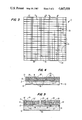
- FIG. 1 is a top plan view of an array of photovoltaic modules formed on a transparent substrate prior to fabrication of the back contacts and prior to electrical isolation of adjacent modules;
- FIG. 2 is an enlarged schematic sectional view taken along line 2--2 of FIG. 1;
- FIG. 3 is a top plan view of the array of FIG. 1 after fabrication of the back contacts and after electrical isolation of the modules in accordance with the present invention
- FIG. 4 is an enlarged schematic sectional view taken along line 4--4 of FIG. 3;
- FIG. 5 is an enlarged schematic sectional view taken along line 5--5 of FIG. 3 showing portions of modules exposed along the walls of inter-module grooves formed during electrical isolation.
- FIGS. 1 and 2 show an array of series-connected, multi-cell photovoltaic modules used, for example, in solar-powered calculators and fabricated according to the method of the present invention.
- the array designated generally by reference numeral 10, is shown in FIGS. 1 and 2 in a state prior to fabrication of the back contacts and prior to electrical isolation of adjacent modules.
- Array 10 is formed on a rectangular flat substrate 12 made of glass or other conventional material transparent to solar radiation.
- Substrate 12 provides a substantially rigid base for the production of the photovoltaic modules and provides physical support for the modules during testing.
- a substantially continuous thin film 13 of transparent conductive oxide material preferably fluorinated tin oxide
- the thickness of transparent conductive oxide film 13 will vary depending upon the desired application of the photovoltaic modules.
- the conductive oxide film of low-light-level modules (such as those used in solar-powered calculators), which typically are tested with light intensities less than about 1 mW/cm 2 , preferably has a thickness of approximately 1700 ⁇ , while highlight-level modules, or "power modules,” preferably have a conductive oxide film thickness of approximately 5000 ⁇ or greater. Power modules are tested at light intensities greater than about 1 mW/cm 2 , typically at approximately 100 mW/cm 2 .
- Conductive oxide film 13 then is scribed in a conventional manner, preferably with a laser, to form parallel first grooves 16 dividing the conductive oxide film into parallel front contact strips 14.
- U.S. Pat. No. 4,292,092 the disclosure of which is incorporated herein by reference to the extent necessary to achieve a thorough understanding of the background of the invention, discloses one suitable laser scribing technique, although certainly not the only suitable technique. Scribing can be performed either by moving the laser beam with respect to the substrate or, preferably, by mounting the substrate on an X-Y table that is movable with respect to the laser beam. Preferably, scribing is done from the front (through substrate 12), although it also can be performed from the back (directly on conductive oxide film 13).
- a substantially continuous thin film 17 of photovoltaic semiconductor material then is fabricated over front contact strips 14 in a conventional manner.
- the semiconductor material of photovoltaic film 17 fills first grooves 16 and provides electrical insulation between adjacent front contact strips 14.
- photovoltaic region 17 is made of hydrogenated amorphous silicon in a PIN structure and is approximately 6,000 ⁇ in thickness, being comprised of a p-layer of 120 ⁇ , and i-layer of 5200-5500 ⁇ , and an n-layer of 500 ⁇ .
- Deposition preferably is by glow discharge in silane, for example, by the method taught by U.S. Pat. No. 4,064,521, the disclosure of which is incorporated herein by reference to the extent necessary to achieve a thorough understanding of the background of the invention.
- Glow discharge can be either DC or RF powered.
- Photovoltaic film 17 then is scribed, preferably by laser scribing, to form second grooves 20 separating adjacent photovoltaic strips 18. Scribing can be performed with the same laser used to scribe the transparent conductive oxide film, except that the power is reduced.
- the photovoltaic film also can be scribed from either side of substrate 12 but preferably is scribed from the front side. Second grooves 20 are scribed adjacent and parallel to first grooves 16 so that photovoltaic strips 18 are parallel to underlying front contact strips 14.
- a substantially continuous film 21 of conductive material next is formed on top of photovoltaic strips 18.
- the conductive material of film 21 fills second grooves 20, forming electrical connections with underlying front contact strips 14.
- Third grooves 24 then are formed in conductive material film 21 parallel and adjacent to second grooves 20 to separate the conductive material film into parallel back contact strips 22.
- Third grooves 24 are formed by chemical etching in a manner well known in the art or by laser scribing.
- chemical etching is used to form third grooves 24, and film 21 also is etched to form a network of fourth grooves 25 that separate the back contacts 22' of adjacent modules (see FIG. 5 also).
- Fourth grooves 25 typically are approximately 750 micrometers in width and correspond in location to the inter-module grooves to be formed subsequently in the laser isolation step discussed below. Fourth grooves 25 are represented by bold lines in FIG. 3 to distinguish them from typically narrower third grooves 24, which are represented by normal lines.
- a laser isolation step then is performed to form inter-module grooves 26, 28 extending through front contact strips 14 and photovoltaic strips 18 without extending into substrate 12 or otherwise damaging the substrate.
- Inter-module grooves 26, 28 separate array 10 into a plurality of discrete photovoltaic modules electrically isolated from each other. For calculator modules, typically between 30 and 120 modules are formed on a single substrate.
- FIG. 3 shows an array of 100 modules formed on substrate 12.
- the laser isolation step forms inter-module grooves 26 parallel to grooves 16, 20, 24 and intermodule grooves 28 orthogonal to grooves 26. As seen in FIGS.
- inter-module grooves 26, 28 are laser scribed along previously etched fourth grooves 25 in back contact film 21.
- inter-module grooves 26 separate array 10 into five multi-cell segments.
- Inter-module grooves 28 divide each segment into a plurality (twenty in the array shown in FIG. 3) of individual photovoltaic modules 30, each of which comprises a plurality (three in FIG. 3) of series-connected photovoltaic cells.
- Each cell includes front contact 14', photovoltaic element 18', and back contact 22'.
- the series connection between adjacent cells in an individual module is accomplished by the conductive material filling second grooves 20, which connects an individual back contact 22' with the underlying front contact 14' of the adjacent cell.
- the laser isolation step can be performed from either side of array 10 but preferably is performed from the front side of array 10, that is, through substrate 12.
- a frequency-doubled neodymium YAG laser emitting light having a wavelength of about 0.53 micrometers in a TEM 00 mode typically is used to form the inter-module grooves 26, 28.
- the laser preferably is focused to less than about 25 micrometers with a depth of field of approximately 500 micrometers and preferably is operated at a power of approximately 100-300 mW with a pulse repetition rate of about 5 kHz and a table feed rate of about 2-10 centimeters per second. Under such scribing conditions, the width of inter-module grooves 26, 28 typically is approximately 25-50 micrometers.
- high-light-level modules having thicker front contact strips are laser scribed, of course, a higher power range generally must be used.
- An electrical resistance of 10-20 megohms between adjacent modules 30 is achievable through the laser isolation step performed under the presently preferred scribing conditions.
- Such a high inter-module resistance ensures that each module on a substrate is electrically isolated from the other modules on the same substrate during testing and curing.
- a minimum inter-module resistance of 1 megohm is required for adequate isolation of low-light-level modules, such as those used in solar-powered calculators, to assure that each module reacts individually when the array is illuminated during testing.
- Highlight-level modules, such as power modules typically can be reliably tested with an inter-module resistance less than 1 megohm.
- the laser isolation step can be performed prior to forming conductive material film 21.
- This embodiment has the advantage of conserving production time where third grooves 24 are formed by chemical etching, because inter-module grooves 26, 28 can be laser scribed in conjunction with the laser scribing of second grooves 20 at the same scribing station.
- back contacts 22' are formed, preferably by conventional silkscreen methods.
- a film 21 of conductive material is formed on top of photovoltaic elements 18 and in second grooves 20 and inter-module grooves 26, 28.
- a resist material is patterned on top of film 21 leaving the portions overlying intermodule grooves 26, 28 and to-be-formed third grooves 24 exposed.
- the exposed portions then are etched with an acid to form third grooves 24 and fourth grooves 25 in film 21 and to remove the conductive material from inter-module grooves 26, 28.
- FIG. 5 is an enlarged view of a section of one wall of an inter-module groove 28.
- the undesirable electrical contacts typically occur in the areas designated by circles A in FIG. 5. Recrystallization of exposed amorphous silicon outside of circle A also can cause problems if it acts to electrically connect, by a more circuitous route, adjacent front contacts 14'.
- the degree of shunting varies with the conditions present during the deposition of the amorphous silicon film and has been particularly evident during higher throughput production of modules, when deposition conditions are more difficult to control. Also, the problem is more severe with low-light level (and consequently lower-current) modules such as those used in solar-powered calculators.
- Plasma etching of array 10 is performed in a conventional manner.
- a resist material (not shown) is formed on the back surfaces of individual modules 30 by, for example, silk-screening to mask them while grooves 26, 28 remain exposed.
- grooves 26 preferably remain exposed to the plasma to eliminate the need for removing the resist material from grooves 26 prior to breaking up the substrate. Resist material spanning grooves 26 would be cosmetically undesirable and would interfere with substrate breakup.
- array 10 is exposed in a conventional manner in a vacuum chamber to a plasma (an electrically ionized gas) that selectively reacts with the semiconductor material exposed in grooves 26, 28 for a prescribed period of time.
- the exposure time should be sufficiently long to enable the plasma to remove the recrystallized silicon exposed on the walls of grooves 28 without excessively undercutting the exposed amorphous silicon elements and without damaging the substrate, which is comprised of glass.
- the plasma and reactant products then are removed from the vacuum chamber by conventional means.
- plasma etching using a mixture of carbon tetrafluoride and oxygen produces substantial increases in yield for low-light-level photovoltaic modules when compared to the same type of modules isolated by laser scribing alone.
- gases effective for etching silicon materials such as fluoroform, hexafluoroethane, chlorotrifluoromethane, sulphur hexafluoride, nitrogen trifluoride, other gases, and mixtures of these gases, also can be used.
- gases effective for etching silicon materials such as fluoroform, hexafluoroethane, chlorotrifluoromethane, sulphur hexafluoride, nitrogen trifluoride, other gases, and mixtures of these gases, also can be used.
- the optimum plasma etching conditions vary with the plasma constituents, the size of the chamber, the number of modules being etched at one time, and the methods used to form the modules.
- an RF-powered ionizer preferably is operated at 200 W and the laser-isolated array preferably is exposed to the resulting plasma for a period of 30-60 seconds.
- a carbon tetrafluoride-oxygen mixture in a ratio of 92:8 at a pressure of 26-47 Pa preferably is used in an RF-powered plasma chamber operated at 2,000 W. Under such plasma etching conditions, the plurality of arrays preferably are exposed to the plasma for approximately 4.5 minutes.
- any etch resist suitable for the plasma employed can be used to mask the individual modules from the plasma etch.
- epoxy to be particularly suitable as a plasma etch resist when used with a carbon tetrafluoride-oxygen plasma, although other resists can be used.
- the epoxy resist need not be removed after plasma etching, because it serves to protect the back contacts of the modules during testing of the array and in the end use of the individual module.
- the efficacy of the plasma etch is illustrated further by the following example comparing the performance of low-light-level photovoltaic modules that were electrically isolated by laser scribing before and after being subjected to plasma etching.
- Each array was subjected to a laser isolation step before the back contact film was deposited, as described above, using a frequency-doubled neodymium YAG laser emitting light of a wavelength of 0.53 micrometers in a TEM 00 mode focused at less than 25 micrometers with a depth of field of approximately 500 micrometers.
- the laser was operated at a power of 240-300 mW with a pulse repetition rate of about 5 kHz and a table feed rate (the speed at which the X-Y table was moved) of approximately 5 centimeters per second to form the inter-module grooves.
- the forty arrays of photovoltaic modules were placed on a light test apparatus having a fluorescent light source with an intensity of 200 lux. Each individual module was tested to determine whether it produced both the minimum acceptable operating voltage of 1.5 volts and minimum acceptable operating current of 6 micro amps. "Yields" were determined by dividing the number of modules in each array exceeding both the minimum operating voltage and minimum operating current when exposed to 200 lux of illumination by the number of modules in the array and multiplying by 100 to obtain the passing percentage. The arrays then were placed twenty at a time in an RF-powered plasma chamber and exposed for approximately 4.5 minutes to a plasma formed from a mixture of carbon tetrafluoride and oxygen in a ratio of 92:8. The plasma chamber was operated at approximately 2000 W, and the gas pressure was approximately 33 Pa.
- each "lot” represents ten arrays, and the reported yields are the aggregate yields for each group of ten arrays.
- the yields obtained after the plasma etch were consistently higher than the yields available before the plasma etch.
- an additional 18-23% improvement in yield was obtained. This improvement occurred despite the differences in the fabrication apparatus from which the tested arrays were taken, the letters L, N, and P in the lot numbers indicating the apparatus used to produce the arrays.
- laser scribing can be performed at wavelengths other than those disclosed in the present application, and different plasmas and resists can be used in etching the inter-module grooves after laser isolation.
- methods other than plasma etching such as mechanical etching or chemical etching (using, for example, an NaOH solution), can be used in place of plasma etching.
- the method also can be performed on other thin-film semiconductor devices fabricated in an array on a substrate, and can be used with devices comprised of semi-crystalline or crystalline semiconductor films.
Abstract
Description
              TABLE I
______________________________________
        Yield        Yield
Array   Before       After      Improvement
Lot No. Plasma Etch  Plasma Etch
                                in % Yield
______________________________________
L-05245-1
        35%          56%        21
L-05285-1
        29%          52%        23
N-05285-1
        75%          93%        18
P-05285-1
        32%          53%        21
______________________________________
Claims (21)
Priority Applications (1)
| Application Number | Priority Date | Filing Date | Title |
|---|---|---|---|
| US06/750,776 US4667058A (en) | 1985-07-01 | 1985-07-01 | Method of fabricating electrically isolated photovoltaic modules arrayed on a substrate and product obtained thereby |
Applications Claiming Priority (1)
| Application Number | Priority Date | Filing Date | Title |
|---|---|---|---|
| US06/750,776 US4667058A (en) | 1985-07-01 | 1985-07-01 | Method of fabricating electrically isolated photovoltaic modules arrayed on a substrate and product obtained thereby |
Publications (1)
| Publication Number | Publication Date |
|---|---|
| US4667058A true US4667058A (en) | 1987-05-19 |
Family
ID=25019119
Family Applications (1)
| Application Number | Title | Priority Date | Filing Date |
|---|---|---|---|
| US06/750,776 Expired - Fee Related US4667058A (en) | 1985-07-01 | 1985-07-01 | Method of fabricating electrically isolated photovoltaic modules arrayed on a substrate and product obtained thereby |
Country Status (1)
| Country | Link |
|---|---|
| US (1) | US4667058A (en) |
Cited By (54)
| Publication number | Priority date | Publication date | Assignee | Title |
|---|---|---|---|---|
| US4705698A (en) * | 1986-10-27 | 1987-11-10 | Chronar Corporation | Isolation of semiconductor contacts |
| US4755475A (en) * | 1986-02-18 | 1988-07-05 | Sanyo Electric Co., Ltd. | Method of manufacturing photovoltaic device |
| WO1988010514A1 (en) * | 1986-04-05 | 1988-12-29 | Chronar Corp. | Stabilization of intraconnections and interfaces |
| US4853081A (en) * | 1987-10-30 | 1989-08-01 | Ibm Corporation | Process for removing contaminant |
| US4874920A (en) * | 1984-06-08 | 1989-10-17 | Semiconductor Energy Laboratory Co., Ltd. | Electronic device manufacturing methods |
| US4882239A (en) * | 1988-03-08 | 1989-11-21 | Minnesota Mining And Manufacturing Company | Light-rechargeable battery |
| US4892592A (en) * | 1987-03-26 | 1990-01-09 | Solarex Corporation | Thin film semiconductor solar cell array and method of making |
| US5155565A (en) * | 1988-02-05 | 1992-10-13 | Minnesota Mining And Manufacturing Company | Method for manufacturing an amorphous silicon thin film solar cell and Schottky diode on a common substrate |
| US5171709A (en) * | 1988-07-25 | 1992-12-15 | International Business Machines Corporation | Laser methods for circuit repair on integrated circuits and substrates |
| US5182230A (en) * | 1988-07-25 | 1993-01-26 | International Business Machines Corporation | Laser methods for circuit repair on integrated circuits and substrates |
| US5432015A (en) * | 1992-05-08 | 1995-07-11 | Westaim Technologies, Inc. | Electroluminescent laminate with thick film dielectric |
| US5593901A (en) * | 1989-09-08 | 1997-01-14 | Amoco/Enron Solar | Monolithic series and parallel connected photovoltaic module |
| US5712199A (en) * | 1990-10-16 | 1998-01-27 | Canon Kabushiki Kaisha | Method for making semiconductor body and photovoltaic device |
| US6077722A (en) * | 1998-07-14 | 2000-06-20 | Bp Solarex | Producing thin film photovoltaic modules with high integrity interconnects and dual layer contacts |
| ES2155414A1 (en) * | 1999-10-26 | 2001-05-01 | Trimboli Longuetto Antonio Adr | Solar photo-cell has configuration of symmetrical sandwich comprising components of photo-anode and photo-cathode substrate, etched with canals containing conductors |
| US20020139411A1 (en) * | 2001-03-29 | 2002-10-03 | Kaneka Corporation | Thin-film solar cell module of see-through type |
| US20040219801A1 (en) * | 2002-04-25 | 2004-11-04 | Oswald Robert S | Partially transparent photovoltaic modules |
| US20040261840A1 (en) * | 2003-06-30 | 2004-12-30 | Advent Solar, Inc. | Emitter wrap-through back contact solar cells on thin silicon wafers |
| US20050176164A1 (en) * | 2004-02-05 | 2005-08-11 | Advent Solar, Inc. | Back-contact solar cells and methods for fabrication |
| US20050172996A1 (en) * | 2004-02-05 | 2005-08-11 | Advent Solar, Inc. | Contact fabrication of emitter wrap-through back contact silicon solar cells |
| US20050172998A1 (en) * | 2004-02-05 | 2005-08-11 | Advent Solar, Inc. | Buried-contact solar cells with self-doping contacts |
| US20060060238A1 (en) * | 2004-02-05 | 2006-03-23 | Advent Solar, Inc. | Process and fabrication methods for emitter wrap through back contact solar cells |
| US20060162766A1 (en) * | 2003-06-26 | 2006-07-27 | Advent Solar, Inc. | Back-contacted solar cells with integral conductive vias and method of making |
| US20070079866A1 (en) * | 2005-10-07 | 2007-04-12 | Applied Materials, Inc. | System and method for making an improved thin film solar cell interconnect |
| US20080143601A1 (en) * | 2006-11-30 | 2008-06-19 | Tenxc Wireless Inc. | Butler matrix implementation |
| WO2008093957A1 (en) * | 2007-01-30 | 2008-08-07 | Lg Innotek Co., Ltd | High frequency module and manufacturing method thereof |
| US20080216887A1 (en) * | 2006-12-22 | 2008-09-11 | Advent Solar, Inc. | Interconnect Technologies for Back Contact Solar Cells and Modules |
| US20080233715A1 (en) * | 2007-03-22 | 2008-09-25 | United Solar Ovonic Llc | Method and apparatus for the laser scribing of ultra lightweight semiconductor devices |
| US20090102502A1 (en) * | 2007-10-22 | 2009-04-23 | Michel Ranjit Frei | Process testers and testing methodology for thin-film photovoltaic devices |
| US20090104342A1 (en) * | 2007-10-22 | 2009-04-23 | Applied Materials, Inc. | Photovoltaic fabrication process monitoring and control using diagnostic devices |
| US20090126786A1 (en) * | 2007-11-13 | 2009-05-21 | Advent Solar, Inc. | Selective Emitter and Texture Processes for Back Contact Solar Cells |
| US20090130827A1 (en) * | 2007-11-02 | 2009-05-21 | Soo Young Choi | Intrinsic amorphous silicon layer |
| US20090142878A1 (en) * | 2007-11-02 | 2009-06-04 | Applied Materials, Inc. | Plasma treatment between deposition processes |
| US20090256581A1 (en) * | 2008-04-14 | 2009-10-15 | Applied Materials, Inc. | Solar parametric testing module and processes |
| US20090308428A1 (en) * | 2006-09-08 | 2009-12-17 | Mitsubishi Heavy Industries, Ltd. | Solar panel and method of manufacturing solar panel |
| US20090308436A1 (en) * | 2008-06-13 | 2009-12-17 | Jae Ho Kim | Thin film type solar cell and method for manufacturing the same |
| US20100012172A1 (en) * | 2008-04-29 | 2010-01-21 | Advent Solar, Inc. | Photovoltaic Modules Manufactured Using Monolithic Module Assembly Techniques |
| US20100132759A1 (en) * | 2009-06-12 | 2010-06-03 | Renhe Jia | Cell isolation on photovoltaic modules for hot spot reduction |
| US20100159634A1 (en) * | 2008-12-19 | 2010-06-24 | Tzay-Fa Su | Edge film removal process for thin film solar cell applications |
| US20100167458A1 (en) * | 2008-12-29 | 2010-07-01 | Yong Woo Shin | Thin film type solar cell and method for manufacturing the same |
| US20100197072A1 (en) * | 2009-01-30 | 2010-08-05 | Tae-Youn Kim | Method of manufacturing a thin film solar cell |
| WO2010123196A1 (en) * | 2009-04-24 | 2010-10-28 | Jusung Engineering Co., Ltd. | Thin film type solar cell, and method for manufacturing the same |
| US20110005458A1 (en) * | 2009-07-13 | 2011-01-13 | Applied Materials, Inc. | Method and apparatus for improving scribe accuracy in solar cell modules |
| US20110008947A1 (en) * | 2009-07-13 | 2011-01-13 | Applied Materials, Inc. | Apparatus and method for performing multifunction laser processes |
| US20110088760A1 (en) * | 2009-10-20 | 2011-04-21 | Applied Materials, Inc. | Methods of forming an amorphous silicon layer for thin film solar cell application |
| US20110318863A1 (en) * | 2010-06-25 | 2011-12-29 | Taiwan Semiconductor Manufacturing Company, Ltd. | Photovoltaic device manufacture |
| US8203071B2 (en) | 2007-01-18 | 2012-06-19 | Applied Materials, Inc. | Multi-junction solar cells and methods and apparatuses for forming the same |
| US20120186625A1 (en) * | 2009-10-01 | 2012-07-26 | Lg Innotek Co,, Ltd | Solar photovoltaic device and a production method for the same |
| CN102117815B (en) * | 2010-01-06 | 2012-12-26 | 京东方科技集团股份有限公司 | Solar battery assembly and preparation method thereof |
| CN103069578A (en) * | 2010-10-05 | 2013-04-24 | Lg伊诺特有限公司 | Photovoltaic device and method for manufacturing same |
| US8728933B1 (en) * | 2011-08-31 | 2014-05-20 | Alta Devices, Inc. | Laser cutting and chemical edge clean for thin-film solar cells |
| WO2015027996A1 (en) | 2013-08-30 | 2015-03-05 | Solibro Hi-Tech Gmbh | Method for producing sub-solar modules using electrically insulating insulation trenches in a thin-layer solar module, and method for producing a thin-layer solar module with such insulation trenches |
| US20170373262A1 (en) * | 2014-12-23 | 2017-12-28 | Stichting Energieonderzoek Centrum Nederland | Method of making a current collecting grid for solar cells |
| US20180254365A1 (en) * | 2015-09-09 | 2018-09-06 | Moohan Co., Ltd. | Thin film type solar cell and method for manufacturing the same |
Citations (2)
| Publication number | Priority date | Publication date | Assignee | Title |
|---|---|---|---|---|
| US4518815A (en) * | 1982-11-24 | 1985-05-21 | Semiconductor Energy Laboratory Co., Ltd. | Photoelectric conversion device |
| US4594471A (en) * | 1983-07-13 | 1986-06-10 | Semiconductor Energy Laboratory Co., Ltd. | Photoelectric conversion device |
-
1985
- 1985-07-01 US US06/750,776 patent/US4667058A/en not_active Expired - Fee Related
Patent Citations (2)
| Publication number | Priority date | Publication date | Assignee | Title |
|---|---|---|---|---|
| US4518815A (en) * | 1982-11-24 | 1985-05-21 | Semiconductor Energy Laboratory Co., Ltd. | Photoelectric conversion device |
| US4594471A (en) * | 1983-07-13 | 1986-06-10 | Semiconductor Energy Laboratory Co., Ltd. | Photoelectric conversion device |
Non-Patent Citations (4)
| Title |
|---|
| S. Yamazaki et al, Conference Record , 17 th IEEE Photovoltaic Specialists Conf. (1984), pp. 206 211. * |
| S. Yamazaki et al, Conference Record, 17th IEEE Photovoltaic Specialists Conf. (1984), pp. 206-211. |
| Y. Tyan et al, Conference Record , 17 th IEEE Photovoltaic Specialists Conf. (1984), pp. 961 964. * |
| Y. Tyan et al, Conference Record, 17th IEEE Photovoltaic Specialists Conf. (1984), pp. 961-964. |
Cited By (83)
| Publication number | Priority date | Publication date | Assignee | Title |
|---|---|---|---|---|
| US4874920A (en) * | 1984-06-08 | 1989-10-17 | Semiconductor Energy Laboratory Co., Ltd. | Electronic device manufacturing methods |
| US4755475A (en) * | 1986-02-18 | 1988-07-05 | Sanyo Electric Co., Ltd. | Method of manufacturing photovoltaic device |
| WO1988010514A1 (en) * | 1986-04-05 | 1988-12-29 | Chronar Corp. | Stabilization of intraconnections and interfaces |
| US4705698A (en) * | 1986-10-27 | 1987-11-10 | Chronar Corporation | Isolation of semiconductor contacts |
| US4892592A (en) * | 1987-03-26 | 1990-01-09 | Solarex Corporation | Thin film semiconductor solar cell array and method of making |
| US4853081A (en) * | 1987-10-30 | 1989-08-01 | Ibm Corporation | Process for removing contaminant |
| US5155565A (en) * | 1988-02-05 | 1992-10-13 | Minnesota Mining And Manufacturing Company | Method for manufacturing an amorphous silicon thin film solar cell and Schottky diode on a common substrate |
| US4882239A (en) * | 1988-03-08 | 1989-11-21 | Minnesota Mining And Manufacturing Company | Light-rechargeable battery |
| US5171709A (en) * | 1988-07-25 | 1992-12-15 | International Business Machines Corporation | Laser methods for circuit repair on integrated circuits and substrates |
| US5182230A (en) * | 1988-07-25 | 1993-01-26 | International Business Machines Corporation | Laser methods for circuit repair on integrated circuits and substrates |
| US5593901A (en) * | 1989-09-08 | 1997-01-14 | Amoco/Enron Solar | Monolithic series and parallel connected photovoltaic module |
| US5712199A (en) * | 1990-10-16 | 1998-01-27 | Canon Kabushiki Kaisha | Method for making semiconductor body and photovoltaic device |
| US5432015A (en) * | 1992-05-08 | 1995-07-11 | Westaim Technologies, Inc. | Electroluminescent laminate with thick film dielectric |
| US5634835A (en) * | 1992-05-08 | 1997-06-03 | Westaim Technologies Inc. | Electroluminescent display panel |
| US5679472A (en) * | 1992-05-08 | 1997-10-21 | Westaim Technologies, Inc. | Electroluminescent laminate and a process for forming address lines therein |
| US5702565A (en) * | 1992-05-08 | 1997-12-30 | Westaim Technologies, Inc. | Process for laser scribing a pattern in a planar laminate |
| US5756147A (en) * | 1992-05-08 | 1998-05-26 | Westaim Technologies, Inc. | Method of forming a dielectric layer in an electroluminescent laminate |
| US6077722A (en) * | 1998-07-14 | 2000-06-20 | Bp Solarex | Producing thin film photovoltaic modules with high integrity interconnects and dual layer contacts |
| ES2155414A1 (en) * | 1999-10-26 | 2001-05-01 | Trimboli Longuetto Antonio Adr | Solar photo-cell has configuration of symmetrical sandwich comprising components of photo-anode and photo-cathode substrate, etched with canals containing conductors |
| US20050148109A1 (en) * | 2000-07-06 | 2005-07-07 | Oswald Robert S. | Partially transparent photovoltaic modules |
| US20060205184A1 (en) * | 2000-07-06 | 2006-09-14 | Oswald Robert S | Partially transparent photovoltaic modules |
| US20020139411A1 (en) * | 2001-03-29 | 2002-10-03 | Kaneka Corporation | Thin-film solar cell module of see-through type |
| US7098395B2 (en) * | 2001-03-29 | 2006-08-29 | Kaneka Corporation | Thin-film solar cell module of see-through type |
| US20040219801A1 (en) * | 2002-04-25 | 2004-11-04 | Oswald Robert S | Partially transparent photovoltaic modules |
| US20060162766A1 (en) * | 2003-06-26 | 2006-07-27 | Advent Solar, Inc. | Back-contacted solar cells with integral conductive vias and method of making |
| US20040261840A1 (en) * | 2003-06-30 | 2004-12-30 | Advent Solar, Inc. | Emitter wrap-through back contact solar cells on thin silicon wafers |
| US7649141B2 (en) | 2003-06-30 | 2010-01-19 | Advent Solar, Inc. | Emitter wrap-through back contact solar cells on thin silicon wafers |
| US7335555B2 (en) | 2004-02-05 | 2008-02-26 | Advent Solar, Inc. | Buried-contact solar cells with self-doping contacts |
| US20060060238A1 (en) * | 2004-02-05 | 2006-03-23 | Advent Solar, Inc. | Process and fabrication methods for emitter wrap through back contact solar cells |
| US20050172998A1 (en) * | 2004-02-05 | 2005-08-11 | Advent Solar, Inc. | Buried-contact solar cells with self-doping contacts |
| US7144751B2 (en) | 2004-02-05 | 2006-12-05 | Advent Solar, Inc. | Back-contact solar cells and methods for fabrication |
| US20050172996A1 (en) * | 2004-02-05 | 2005-08-11 | Advent Solar, Inc. | Contact fabrication of emitter wrap-through back contact silicon solar cells |
| US20090320922A1 (en) * | 2004-02-05 | 2009-12-31 | Advent Solar, Inc. | Contact Fabrication of Emitter Wrap-Through Back Contact Silicon Solar Cells |
| US7863084B2 (en) | 2004-02-05 | 2011-01-04 | Applied Materials, Inc | Contact fabrication of emitter wrap-through back contact silicon solar cells |
| US20050176164A1 (en) * | 2004-02-05 | 2005-08-11 | Advent Solar, Inc. | Back-contact solar cells and methods for fabrication |
| US20070079866A1 (en) * | 2005-10-07 | 2007-04-12 | Applied Materials, Inc. | System and method for making an improved thin film solar cell interconnect |
| US20090308428A1 (en) * | 2006-09-08 | 2009-12-17 | Mitsubishi Heavy Industries, Ltd. | Solar panel and method of manufacturing solar panel |
| US20080143601A1 (en) * | 2006-11-30 | 2008-06-19 | Tenxc Wireless Inc. | Butler matrix implementation |
| US20080216887A1 (en) * | 2006-12-22 | 2008-09-11 | Advent Solar, Inc. | Interconnect Technologies for Back Contact Solar Cells and Modules |
| US20110126878A1 (en) * | 2006-12-22 | 2011-06-02 | Peter Hacke | Interconnect technologies for back contact solar cells and modules |
| US8203071B2 (en) | 2007-01-18 | 2012-06-19 | Applied Materials, Inc. | Multi-junction solar cells and methods and apparatuses for forming the same |
| WO2008093957A1 (en) * | 2007-01-30 | 2008-08-07 | Lg Innotek Co., Ltd | High frequency module and manufacturing method thereof |
| US7964476B2 (en) | 2007-03-22 | 2011-06-21 | United Solar Ovonic Llc | Method and apparatus for the laser scribing of ultra lightweight semiconductor devices |
| US20080233715A1 (en) * | 2007-03-22 | 2008-09-25 | United Solar Ovonic Llc | Method and apparatus for the laser scribing of ultra lightweight semiconductor devices |
| WO2009055262A1 (en) * | 2007-10-22 | 2009-04-30 | Applied Materials, Inc. | Photovoltaic fabrication process monitoring and control using diagnostic devices |
| US20090104342A1 (en) * | 2007-10-22 | 2009-04-23 | Applied Materials, Inc. | Photovoltaic fabrication process monitoring and control using diagnostic devices |
| US20090102502A1 (en) * | 2007-10-22 | 2009-04-23 | Michel Ranjit Frei | Process testers and testing methodology for thin-film photovoltaic devices |
| US20090130827A1 (en) * | 2007-11-02 | 2009-05-21 | Soo Young Choi | Intrinsic amorphous silicon layer |
| US7741144B2 (en) | 2007-11-02 | 2010-06-22 | Applied Materials, Inc. | Plasma treatment between deposition processes |
| US20090142878A1 (en) * | 2007-11-02 | 2009-06-04 | Applied Materials, Inc. | Plasma treatment between deposition processes |
| US20090126786A1 (en) * | 2007-11-13 | 2009-05-21 | Advent Solar, Inc. | Selective Emitter and Texture Processes for Back Contact Solar Cells |
| US8049521B2 (en) | 2008-04-14 | 2011-11-01 | Applied Materials, Inc. | Solar parametric testing module and processes |
| US20090256581A1 (en) * | 2008-04-14 | 2009-10-15 | Applied Materials, Inc. | Solar parametric testing module and processes |
| US20110067751A1 (en) * | 2008-04-29 | 2011-03-24 | Meakin David H | Photovoltaic modules manufactured using monolithic module assembly techniques |
| US20100012172A1 (en) * | 2008-04-29 | 2010-01-21 | Advent Solar, Inc. | Photovoltaic Modules Manufactured Using Monolithic Module Assembly Techniques |
| US8889470B2 (en) * | 2008-06-13 | 2014-11-18 | Jusung Engineering Co., Ltd. | Thin film type solar cell and method for manufacturing the same |
| US20090308436A1 (en) * | 2008-06-13 | 2009-12-17 | Jae Ho Kim | Thin film type solar cell and method for manufacturing the same |
| US8071420B2 (en) | 2008-12-19 | 2011-12-06 | Applied Materials, Inc. | Edge film removal process for thin film solar cell applications |
| US20100159634A1 (en) * | 2008-12-19 | 2010-06-24 | Tzay-Fa Su | Edge film removal process for thin film solar cell applications |
| US20100167458A1 (en) * | 2008-12-29 | 2010-07-01 | Yong Woo Shin | Thin film type solar cell and method for manufacturing the same |
| US8298852B2 (en) | 2008-12-29 | 2012-10-30 | Jusung Engineering Co., Ltd. | Thin film type solar cell and method for manufacturing the same |
| US8361826B2 (en) * | 2009-01-30 | 2013-01-29 | Lg Display Co., Ltd. | Method of manufacturing a thin film solar cell |
| US20100197072A1 (en) * | 2009-01-30 | 2010-08-05 | Tae-Youn Kim | Method of manufacturing a thin film solar cell |
| WO2010123196A1 (en) * | 2009-04-24 | 2010-10-28 | Jusung Engineering Co., Ltd. | Thin film type solar cell, and method for manufacturing the same |
| US20100313929A1 (en) * | 2009-06-12 | 2010-12-16 | Renhe Jia | Cell isolation on photovoltaic modules for hot spot reduction |
| US20100132759A1 (en) * | 2009-06-12 | 2010-06-03 | Renhe Jia | Cell isolation on photovoltaic modules for hot spot reduction |
| US20110005458A1 (en) * | 2009-07-13 | 2011-01-13 | Applied Materials, Inc. | Method and apparatus for improving scribe accuracy in solar cell modules |
| US20110008947A1 (en) * | 2009-07-13 | 2011-01-13 | Applied Materials, Inc. | Apparatus and method for performing multifunction laser processes |
| US20120186625A1 (en) * | 2009-10-01 | 2012-07-26 | Lg Innotek Co,, Ltd | Solar photovoltaic device and a production method for the same |
| US20110088760A1 (en) * | 2009-10-20 | 2011-04-21 | Applied Materials, Inc. | Methods of forming an amorphous silicon layer for thin film solar cell application |
| CN102117815B (en) * | 2010-01-06 | 2012-12-26 | 京东方科技集团股份有限公司 | Solar battery assembly and preparation method thereof |
| US8563351B2 (en) * | 2010-06-25 | 2013-10-22 | Taiwan Semiconductor Manufacturing Co., Ltd. | Method for manufacturing photovoltaic device |
| US20140014176A1 (en) * | 2010-06-25 | 2014-01-16 | Taiwan Semiconductor Manufacturing Co., Ltd. | Method for manufacturing photovoltaic device |
| US20110318863A1 (en) * | 2010-06-25 | 2011-12-29 | Taiwan Semiconductor Manufacturing Company, Ltd. | Photovoltaic device manufacture |
| US9202947B2 (en) * | 2010-06-25 | 2015-12-01 | Taiwan Semiconductor Manufacturing Co., Ltd. | Photovoltaic device |
| CN103069578A (en) * | 2010-10-05 | 2013-04-24 | Lg伊诺特有限公司 | Photovoltaic device and method for manufacturing same |
| CN103069578B (en) * | 2010-10-05 | 2016-08-10 | Lg伊诺特有限公司 | Photovoltaic device and manufacture method thereof |
| US8728933B1 (en) * | 2011-08-31 | 2014-05-20 | Alta Devices, Inc. | Laser cutting and chemical edge clean for thin-film solar cells |
| WO2015027996A1 (en) | 2013-08-30 | 2015-03-05 | Solibro Hi-Tech Gmbh | Method for producing sub-solar modules using electrically insulating insulation trenches in a thin-layer solar module, and method for producing a thin-layer solar module with such insulation trenches |
| DE102013109478A1 (en) | 2013-08-30 | 2015-03-05 | Hanergy Holding Group Ltd. | Method for producing sub-solar modules by electrically insulating isolation trenches in a thin-film solar module and method for producing a thin-film solar module with such isolation trenches |
| US20170373262A1 (en) * | 2014-12-23 | 2017-12-28 | Stichting Energieonderzoek Centrum Nederland | Method of making a current collecting grid for solar cells |
| US11581502B2 (en) * | 2014-12-23 | 2023-02-14 | Nederlandse Organisatie Voortoegepast-Natuurwetenschappelijk Onderzoek Tno | Method of making a current collecting grid for solar cells |
| US20180254365A1 (en) * | 2015-09-09 | 2018-09-06 | Moohan Co., Ltd. | Thin film type solar cell and method for manufacturing the same |
Similar Documents
| Publication | Publication Date | Title |
|---|---|---|
| US4667058A (en) | Method of fabricating electrically isolated photovoltaic modules arrayed on a substrate and product obtained thereby | |
| US4783421A (en) | Method for manufacturing electrical contacts for a thin-film semiconductor device | |
| US4892592A (en) | Thin film semiconductor solar cell array and method of making | |
| US4854974A (en) | Electrical contacts for a thin-film semiconductor device | |
| KR910006676B1 (en) | Large area photovoltage cells and method of producing said cells | |
| US5131954A (en) | Monolithic solar cell array and method for its manufacturing | |
| KR100217006B1 (en) | Etching method, process for producing a semiconductor element using said etching method, and apparatus suitable for practicing said etching method | |
| EP0260821B1 (en) | Conversion process for passivating short circuit current paths im semiconductor devices and articles thereby produced | |
| US4485264A (en) | Isolation layer for photovoltaic device and method of producing same | |
| US4419530A (en) | Solar cell and method for producing same | |
| JP3809237B2 (en) | Electrolytic pattern etching method | |
| US4451970A (en) | System and method for eliminating short circuit current paths in photovoltaic devices | |
| JP3414738B2 (en) | Integrated laser patterning method for thin film solar cells | |
| CA1209234A (en) | System and method for eliminating short and latent short circuit current paths in photovoltaic devices | |
| JPH0738125A (en) | Method and apparatus for manufacturing solar cell, method and chamber for depositing amorphous silicon | |
| JPH0472392B2 (en) | ||
| EP2184789A1 (en) | Method and apparatus for manufacturing thin film photoelectric conversion module | |
| JP3618865B2 (en) | Photovoltaic element characteristic inspection apparatus and manufacturing method | |
| US4948740A (en) | Method for the integrated series-interconnection of thick-film solar cells and method for the manufacture of tandem solar cells | |
| EP2283523A2 (en) | Assembly line for photovoltaic devices | |
| US20100190275A1 (en) | Scribing device and method of producing a thin-film solar cell module | |
| JPS6154681A (en) | Manufacture of thin-film photovoltaic element | |
| JPH0572756B2 (en) | ||
| JPH10209475A (en) | Manufacture of integrated photovoltaic device | |
| JP2966332B2 (en) | Method and apparatus for manufacturing photovoltaic element |
Legal Events
| Date | Code | Title | Description |
|---|---|---|---|
| AS | Assignment |
Owner name: SOLAREX CORPORATION 1335 PICCARD DRIVE ROCKVILLE, Free format text: ASSIGNMENT OF ASSIGNORS INTEREST.;ASSIGNORS:CATALANO, ANTHONY W.;D'AIELLO, ROBERT V.;BREWER, JOHN A.;REEL/FRAME:004447/0879 Effective date: 19850729 Owner name: SOLAREX CORPORATION 1335 PICCARD DRIVE , ROCKVILLE Free format text: ASSIGNMENT OF ASSIGNORS INTEREST.;ASSIGNOR:PODLESNY, RICHARD J.;REEL/FRAME:004447/0873 Effective date: 19850729 |
|
| FEPP | Fee payment procedure |
Free format text: PAYOR NUMBER ASSIGNED (ORIGINAL EVENT CODE: ASPN); ENTITY STATUS OF PATENT OWNER: LARGE ENTITY |
|
| FPAY | Fee payment |
Year of fee payment: 4 |
|
| FEPP | Fee payment procedure |
Free format text: PAYOR NUMBER ASSIGNED (ORIGINAL EVENT CODE: ASPN); ENTITY STATUS OF PATENT OWNER: LARGE ENTITY Free format text: PAYER NUMBER DE-ASSIGNED (ORIGINAL EVENT CODE: RMPN); ENTITY STATUS OF PATENT OWNER: LARGE ENTITY |
|
| FEPP | Fee payment procedure |
Free format text: PAYOR NUMBER ASSIGNED (ORIGINAL EVENT CODE: ASPN); ENTITY STATUS OF PATENT OWNER: LARGE ENTITY Free format text: PAYER NUMBER DE-ASSIGNED (ORIGINAL EVENT CODE: RMPN); ENTITY STATUS OF PATENT OWNER: LARGE ENTITY |
|
| FEPP | Fee payment procedure |
Free format text: PAYER NUMBER DE-ASSIGNED (ORIGINAL EVENT CODE: RMPN); ENTITY STATUS OF PATENT OWNER: LARGE ENTITY Free format text: PAYOR NUMBER ASSIGNED (ORIGINAL EVENT CODE: ASPN); ENTITY STATUS OF PATENT OWNER: LARGE ENTITY |
|
| FPAY | Fee payment |
Year of fee payment: 8 |
|
| AS | Assignment |
Owner name: AMOCO/ENRON SOLAR, MARYLAND Free format text: ASSIGNMENT OF ASSIGNORS INTEREST;ASSIGNORS:AMOCO CORPORATION;SOLAREX CORPORATION;REEL/FRAME:007289/0064 Effective date: 19950101 |
|
| REMI | Maintenance fee reminder mailed | ||
| LAPS | Lapse for failure to pay maintenance fees | ||
| FP | Lapsed due to failure to pay maintenance fee |
Effective date: 19990519 |
|
| AS | Assignment |
Owner name: BIOSTRATUM AB, SWEDEN Free format text: ASSIGNMENT OF ASSIGNORS INTEREST;ASSIGNOR:TRYGGVASON, KARL;REEL/FRAME:010776/0266 Effective date: 20000324 |
|
| STCH | Information on status: patent discontinuation |
Free format text: PATENT EXPIRED DUE TO NONPAYMENT OF MAINTENANCE FEES UNDER 37 CFR 1.362 |