US4654697A - Video signal apparatus for processing a time-division-multiplex video signal having a buffer segment - Google Patents

Video signal apparatus for processing a time-division-multiplex video signal having a buffer segment Download PDF

Info

Publication number
US4654697A
US4654697A US06/793,810 US79381085A US4654697A US 4654697 A US4654697 A US 4654697A US 79381085 A US79381085 A US 79381085A US 4654697 A US4654697 A US 4654697A
Authority
US
United States
Prior art keywords
segment
signal
video signal
compressed
time
Prior art date
Legal status (The legal status is an assumption and is not a legal conclusion. Google has not performed a legal analysis and makes no representation as to the accuracy of the status listed.)
Expired - Fee Related
Application number
US06/793,810
Inventor
Steven J. Sasson
Current Assignee (The listed assignees may be inaccurate. Google has not performed a legal analysis and makes no representation or warranty as to the accuracy of the list.)
Eastman Kodak Co
Original Assignee
Eastman Kodak Co
Priority date (The priority date is an assumption and is not a legal conclusion. Google has not performed a legal analysis and makes no representation as to the accuracy of the date listed.)
Filing date
Publication date
Application filed by Eastman Kodak Co filed Critical Eastman Kodak Co
Priority to US06/793,810 priority Critical patent/US4654697A/en
Assigned to EASTMAN KODAK COMPANY, A NEW JERSEY CORP. reassignment EASTMAN KODAK COMPANY, A NEW JERSEY CORP. ASSIGNMENT OF ASSIGNORS INTEREST. Assignors: SASSON, STEVEN J.
Application granted granted Critical
Publication of US4654697A publication Critical patent/US4654697A/en
Anticipated expiration legal-status Critical
Expired - Fee Related legal-status Critical Current

Links

Images

Classifications

    • HELECTRICITY
    • H04ELECTRIC COMMUNICATION TECHNIQUE
    • H04NPICTORIAL COMMUNICATION, e.g. TELEVISION
    • H04N11/00Colour television systems
    • H04N11/06Transmission systems characterised by the manner in which the individual colour picture signal components are combined
    • H04N11/12Transmission systems characterised by the manner in which the individual colour picture signal components are combined using simultaneous signals only

Definitions

  • this invention relates to video signal apparatus. More particularly, this invention relates to apparatus for processing time-divisionmultiplex video signals which have a buffer segment between video component segments.
  • VCR Consumer video cassette recorders
  • VCR Consumer video cassette recorders
  • the luminance component of the video signal is converted to an FM signal and the chrominance component is converted to a lower frequency signal outside of the frequency band of the FM luminance signal.
  • the "color-under” format has several disadvantages. Thus, the resolution of the image is reduced due to reduction of the luminance bandwidth. In addition, color inaccuracies may result from the poor chrominance signal to noise ratio and from errors in the generation and regeneration of the standard composite color subcarrier signal.
  • This patent also discloses insertion of a mezzanine signal of fixed voltage level between the sequential chrominance and luminance components to serve as a dynamic reference for subsequent processing of the chrominance component.
  • a somewhat similar technique is disclosed in U.S. Pat. No. 4,084,181, issued Apr. 11, 1978, for "APPARATUS FOR TRANSMISSION OF CHROMINANCE SIGNALS DURING BLANKING PERIOD", in which only the chrominance component signal is compressed in time and inserted during the horizontal blanking period.
  • This patent also discloses insertion of fixed level buffers between the chrominance and luminance signals and between the chrominance and synchronizing signals to reduce crosstalk.
  • the limited response time of the analog path to large changes in signal value may cause distortion of a sequentially transmitted component signal resulting in degradation and color changes in a reproduced image.
  • a fixed level buffer is used to isolate components of the video signal processed by the system, the fixed level of the signal during the buffer does not always insure that the signal reaches an appropriate value before transmission or production of the next signal component.
  • apparatus for processing a time-division-multiplex video signal in which the response time of an output transmission path to which the TDM signal is applied, is compensated for, during buffer segments between compressed component segments of the TDM signal.
  • the TDM signal is thus transmitted along the path without distortion, resulting in a reproduced image which has not been degraded and the color of which is accurate.
  • the TDM signal has first and second compressed segments each of which includes a series of time-compressed samples of varying signal value representing one or the other respectively of luminance and chrominance components of a color video signal.
  • a buffer segment is formed between the first and second segments.
  • the signal value of the TDM signal is caused to change from the signal value of the last sample of the first segment to the signal value of the first sample of the second segment, by applying to the output transmission path the signal value of the first sample of the second segment.
  • the true signal value of the first sample of the second segment is applied to the path insuring accurate image reproduction and color rendition.
  • video signal apparatus includes circuit means for providing to an output transmission path a time-division-multiplex (TDM) video signal (1) having a first compressed segment including a series of time-compressed samples of varying signal value representing one of the luminance and chrominance components of a color video signal and (2) having a second compressed segment, sequential in time to said first segment, said second segment including a series of time compressed samples of varying signal value representing the other of luminance and chrominance components of said color video signal.
  • TDM time-division-multiplex
  • the apparatus includes control means for controlling the circuit means to form a buffer segment between said first and second compressed segments and to apply the signal value of the first sample of the second segment to said output path during the buffer segment to cause the signal value of the TDM signal to change to the value of said first sample before application of said sample to said output path. In this manner, the response time of the output path is compensated for to permit distortion-free transmission of the samples of the second segment.
  • FIG. 1 is a block diagram of video signal apparatus incorporating the present invention
  • FIG. 2 is a block diagram of the TDM record circuit of the apparatus FIG. 1;
  • FIG. 3 is a block diagram of the TDM playback circuit of the apparatus of FIG. 1;
  • FIG. 4 is a block diagram of the signal generator and TDM control circuit of the apparatus of FIG. 1;
  • FIG. 5A is an illustrative diagram of a TDM video signal
  • FIG. 5B and FIG. 5C are respectively general and specific timing diagrams for the TDM signal of FIG. 5A;
  • FIG. 6 is a signal value versus time diagram of the horizontal segment of the signal of FIG. 5A.
  • FIG. 7 is a diagram of a TDM buffer segment illustrating the present invention.
  • apparatus 10 includes a video signal source 12 which may for example be a color video camera or a transmission source such as a broadcast, satellite or cable transmission system.
  • a video signal source 12 supplies a standard NTSC composite color video signal used in the U.S. It will be appreciated, however that other composite video signal systems such as the PAL and SECAM systems used in other parts of the world may also be processed in accordance with the present invention.
  • source 12 may provide component video signals such as a YIQ component video signal or an RGB component video signal.
  • the color video signal is supplied to a TDM record circuit 14 which converts the NTSC composite color video signal into a TDM video signal which is recorded on magnetic tape by means of magnetic tape assembly 16.
  • Assembly 16 may, for example, be of a type used in consumer video cassette recorders. In such VCRs a rotating magnetic head or heads records the video signal in magnetic tracks that are slanted across the width of tape contained in a cassette.
  • Apparatus 10 also includes TDM playback circuit 18 which receives signals from magnetic tape assembly 16 and converts the TDM video signal to a composite color video signal or component color video signal which is applied to monitor 20 for display of video images.
  • a signal generator and TDM control 22 is also provided for providing frequency signals and control signals to circuits 14 and 18.
  • video signal source 12, circuits 14, 18, assembly 16, and circuit 22 may be combined into a lightweight camera/recorder for use in recording still and movie type image sequences.
  • TDM record and playback circuits 14 and 18, magnetic tape assembly 16, and control 22 may be combined into a single apparatus which functions as a video cassette recorder/player or that TDM playback circuit 18, magnetic tape assembly 16, and control 22 may be combined into a single apparatus which only plays back prerecorded video cassettes.
  • Other combinations will be apparent to those skilled in the art including the combining of the TDM signal processing circuit of circuits 14 and 18 with conventional signal processing circuits as disclosed in commonly-assigned copending U.S. patent application Ser. No. 725,873, by Carl Schauffele, entitled VIDEO REPRODUCTION APPARATUS, filed Apr. 22, 1985.
  • TDM record circuit 14 of the apparatus of FIG. 1.
  • the function of circuit 14 is to convert a composite color video signal in which the luminance and chrominance components occupy concurrent, overlapping frequency bandwidths into a time-division-multiplex video signal in which the luminance and chrominance components are separated and transmitted in time sequential manner in order to avoid time base errors, image degradation and color inaccuracies which may result if the composite video signal was recorded on magnetic tape.
  • the TDM signal has a horizontal line duration (which in the NTSC system is equal to approximately 63.5 msec).
  • the TDM signal includes a series of segments which are processed in a time sequential manner.
  • TDM signal 24 includes H sync segment 26, compressed Q chrominance segment 28, first buffer segment 30, compressed I chrominance segment 32, second buffer segment 34, and compressed Y luminance segment 36.
  • H sync segment 26 includes a compressed horizontal sync portion 26A which has a duration from time t 0 to t 1 ; a black level portion 26B which has a duration from t 1 to t 2 and a chrominance level portion 26C which has a duration from time t 2 to time t 3 .
  • Q chrominance segment 28 has a duration from time t 3 to time t 4
  • first buffer segment 30 has a duration from t 4 to t 5
  • I chrominance segment 32 has a duration from t 5 to t 6
  • second buffer segment 34 has a duration from t 6 to t 7
  • Y luminance segment 36 has a duration from t 7 to t 8 (FIGS. 5A and 5B).
  • TDM record circuit 14 receives a composite color video signal from source 12 (FIG. 1). This signal is applied to YIQ separator 38 which separates the I and Q chrominance components from the Y luminance component and may, for example, include a comb filter and chrominance demodulator (not shown). The separated Y, I and Q analog signal components are respectively applied to analog-to-digital converters (ADC) 40, 42, and 44. ADC 44 samples the Q chrominance analog signal at a frequency F 1 and converts these analog samples to digital samples which are written into Q memory 46 at the F 1 sampling frequency.
  • ADC analog-to-digital converters
  • the I analog chrominance component is sampled at a frequency F 2 by ADC 42 and converted to digital samples which are stored in I memory 48 at the frequency of signal F 2 .
  • the Y luminance analog signal is sampled by ADC 40 at a frequency F 3 and converted to digital samples which are stored in Y memory 50 at the sampling frequency F 3 .
  • Frequencies F 1 , F 2 , and F 3 are chosen so as to be at least twice the highest frequency of each of the components sampled. As disclosed in the above described Schauffele U.S. patent application Ser. No. 725,873, the frequency F 1 may for example be chosen to be 2.013 MHz.; frequency F 2 may be chosen to have a frequency of 4.027 MHz and frequency F 3 may be chosen to be 14.097 MHz.
  • the I and Q chrominance components and Y luminance component are compressed in time and rearranged in a time sequential fashion.
  • a sampling frequency F 4 is chosen to effect production of the TDM signal during a single horizontal line period.
  • frequency F 4 may be chosen at 18.125 MHz and this frequency is sequentially applied to Q memory 46, I memory 48 and Y memory 50 to produce the TDM signal.
  • Timing may be further simplified by making the durations of each of the TDM segments integrally divisible by the same number, in this case 9, so that timing may be effected by a slower, less costly, less complex timing circuit (see copending U.S. patent application Ser. No. 793,820, filed Nov 11, 1985, entitled APPARATUS FOR PROCESSING A TIME-DIVISION-MULTIPLEX VIDEO SIGNAL HAVING SEGMENT DURATIONS DIVISIBLE BY A COMMON NUMBER).
  • Signal generator and TDM control circuit 22 provides the timing for processing the TDM signal shown in FIG. 5A.
  • signal generator 52 (which may be of a type known to those skilled in the art) produces signals having frequencies F 1 , F 2 , F 3 , and F 4 .
  • the F 1 , F 2 , and F 3 signals are respectively supplied to circuit 14 and, as described above, signal F 4 is also supplied to a divide by N circuit 54.
  • N is 9 in order to produce a signal F 5 having a frequency which is 1/9 of the frequency of F 4 . Since signal F 4 has a frequency equal to 1152 F H , signal F 5 has a frequency equal to 1/9 of F 4 or 128 F H .
  • TDM segments The timing of TDM segments is effected by counting the periods of signal F 5 by a seven-bit counter 56 having output terminals labeled "1", “2”, “ 4", “8", "16", “32”, and "64". The output of these terminals are selectively applied to AND gates 58, 60, 62, 64, 66, 68, 70, and 72 to produce respective control signals C 1 , C 2 , C 3 , C 4 , C 5 , C 6 , C 7 , and C 8 .
  • TDM video signal is initiated at a suitable time t 0 which corresponds to the delayed leading edge of the horizontal sync pulse of the composite video signal.
  • the TDM signal is applied to an output transmission path 78 such as wire, cable or the like.
  • counter 56 begins counting pulses of frequency F 5
  • H segment processor 74 initiates the production of segment 26.
  • compressed sync portion 26A is produced; from time t 1 to t 2 (count 2 to count 4) black level portion 26B is produced; and from t 2 to t 3 , (count 4 to count 6) chrominance level portion 26C is produced.
  • Timing is effected by the control signals C 1 , C 2 and C 3 applied to processor 74.
  • control signal C 3 is also applied to Q memory 46 (FIG. 2) to initiate formation of Q segment 28 by reading out digital samples of the Q chrominance component at the time-compression sampling frequency F 4 .
  • DAC 76 converts the digital samples to analog samples and applies them in series to output path 76.
  • a buffer segment 30 is formed between segments 28 and 32 in order to isolate these segments and to allow the TDM signal to change to an appropriate value to compensate for the response time of transmission path 78. If the response to large changes in signal value is insufficient, the first samples of the next TDM component segment may be distorted, resulting in image degradation and color inaccuracies in a reproduced image.
  • the formation of buffer segment 30 is illustrated in FIG. 7. As shown, the last samples Q n-2 , Q n-1 , Q n of Q segment 28 are separated by buffer segment 30 from the first samples I 1 , I 2 , I 3 , of I segment 32.
  • FIG. 7 shows the signal values of the Q and I samples to be have voltage levels which would be produced after the digital signals read out of memories 46 and 48 (FIG. 2) are converted to analog signals by digital to analog converter (DAC) 76.
  • DAC digital to analog converter
  • control signal C 5 terminates buffer segment 30 and initiates reading out of samples from I memory 48 to produce I segment 32.
  • control signal C 6 terminates the reading out of samples from I memory 48 and applies the value of the first sample of the Y luminance signal to output path 78 during the duration of buffer segment 34.
  • control signal C 7 initiates the reading out of Y samples from Y memory 50 to produce segment 36.
  • the TDM signal is modulated onto an FM carrier by FM modulator 80 (see FIG. 2) and the FM signal supplied to magnetic tape assembly 16 to be recorded on magnetic tape.
  • TDM playback circuit 18 As shown, a TDM signal played back from magnetic tape by assembly 16 is supplied to FM demodulator 82 which demodulates the TDM signal.
  • the first segment 26 of the TDM signal is applied to H sync processor 84 which samples the sync, black and chrominance levels of segment portions 26A, 26B, and 26C and produces a composite horizontal sync and blanking signal at an appropriate time.
  • the chrominance level signal is also used to control the level of the I and Q chrominance components by means not shown.
  • the Q chrominance segment 28 is sampled by analog-to-digital converter (ADC) 86 at the sampling frequency F 4 and written into Q memory 88.
  • ADC analog-to-digital converter
  • control signal C 5 initiates reading into I memory 90, samples of I segment 32 at the frequency sampling rate of F 4 . Reading into I memory is terminated at time t 6 by control signal C 6 . Samples of Y segment 36 produced by ADC 86 are written into Y memory 92 from t 7 to t 8 .
  • H sync processor 84 After an appropriate delay to allow reading into memories 88, 90, and 92 of the respective Q, I and Y samples, H sync processor 84 produces a composite horizontal sync and blanking signal which is applied to composite video processing circuit 94.
  • the respective digital samples are converted by digital to analog converters (DAC) 96, 98, and 100 into appropriate Q chrominance, I chrominance and Y luminance signals which are applied to composite video signal processing circuit 94 to produce a composite NTSC color video signal which is applied to monitor 20.
  • DAC digital to analog converters

Abstract

Video signal apparatus processes a time-division-multiplex (TDM) video signal which has a buffer segment between luminance and chrominance component segments. The apparatus includes a circuit which provides to an output transmission path, a TDM video signal having a compressed luminance segment including a series of time-compressed samples of varying signal value representing the luminance component of a color video signal and a compressed chrominance segment including a series of time-compressed samples of varying signal value representing the chrominance component of the color video signal. A control controls the circuit to form a buffer segment between the luminance and chrominance segments. During the buffer segment, the signal value of the TDM signal is caused to change from the value of the last sample of one segment to the value of the first sample of the next segment by applying to the output transmission path the signal value of the first sample of the next segment.

Description

BACKGROUND OF THE INVENTION
In general, this invention relates to video signal apparatus. More particularly, this invention relates to apparatus for processing time-divisionmultiplex video signals which have a buffer segment between video component segments.
Consumer video cassette recorders (VCR) typically use a "color-under" format to minimize color image problems which may result from the direct recording of a composite color video signal on magnetic tape. In the "color-under" format, the luminance component of the video signal is converted to an FM signal and the chrominance component is converted to a lower frequency signal outside of the frequency band of the FM luminance signal. The "color-under" format has several disadvantages. Thus, the resolution of the image is reduced due to reduction of the luminance bandwidth. In addition, color inaccuracies may result from the poor chrominance signal to noise ratio and from errors in the generation and regeneration of the standard composite color subcarrier signal.
In order to minimize these disadvantages of the "color-under" format, it has been proposed in U.S. Pat. No. 4,335,393, issued June 15, 1982, for "METHOD AND SYSTEM USING SEQUENTIALLY ENCODED COLOR AND LUMINANCE PROCESSING OF VIDEO TYPE SIGNALS TO IMPROVE PICTURE QUALITY", patentee G. J. Pearson, to reformat the concurrent luminance and chrominance components of a composite color video signal into a signal having compressed luminance and chrominance signals which are sequential in time to one another. The time sequential signal is then recorded on magnetic tape. This patent also discloses insertion of a mezzanine signal of fixed voltage level between the sequential chrominance and luminance components to serve as a dynamic reference for subsequent processing of the chrominance component. A somewhat similar technique is disclosed in U.S. Pat. No. 4,084,181, issued Apr. 11, 1978, for "APPARATUS FOR TRANSMISSION OF CHROMINANCE SIGNALS DURING BLANKING PERIOD", in which only the chrominance component signal is compressed in time and inserted during the horizontal blanking period. This patent also discloses insertion of fixed level buffers between the chrominance and luminance signals and between the chrominance and synchronizing signals to reduce crosstalk. In "NTT and NHK Home Systems for Sharp TV", ELECTRONICS, July 14, 1983, pages 82-3, there is disclosed a high definition color video signal in which the chrominance signal is compressed and transmitted sequentially in time relative to the luminance signal. A fixed level guard signal is inserted between the two signals.
In the transmission of a time-division-multiplex video signal over an analog transmission path, the limited response time of the analog path to large changes in signal value, may cause distortion of a sequentially transmitted component signal resulting in degradation and color changes in a reproduced image. Although, in each of the above systems a fixed level buffer is used to isolate components of the video signal processed by the system, the fixed level of the signal during the buffer does not always insure that the signal reaches an appropriate value before transmission or production of the next signal component.
SUMMARY OF THE INVENTION
According to the present invention, there is provided apparatus for processing a time-division-multiplex video signal in which the response time of an output transmission path to which the TDM signal is applied, is compensated for, during buffer segments between compressed component segments of the TDM signal. The TDM signal is thus transmitted along the path without distortion, resulting in a reproduced image which has not been degraded and the color of which is accurate. The TDM signal has first and second compressed segments each of which includes a series of time-compressed samples of varying signal value representing one or the other respectively of luminance and chrominance components of a color video signal. A buffer segment is formed between the first and second segments. During the buffer segment, the signal value of the TDM signal is caused to change from the signal value of the last sample of the first segment to the signal value of the first sample of the second segment, by applying to the output transmission path the signal value of the first sample of the second segment. Thus, the true signal value of the first sample of the second segment is applied to the path insuring accurate image reproduction and color rendition.
According to an aspect of the present invention, video signal apparatus includes circuit means for providing to an output transmission path a time-division-multiplex (TDM) video signal (1) having a first compressed segment including a series of time-compressed samples of varying signal value representing one of the luminance and chrominance components of a color video signal and (2) having a second compressed segment, sequential in time to said first segment, said second segment including a series of time compressed samples of varying signal value representing the other of luminance and chrominance components of said color video signal. The apparatus includes control means for controlling the circuit means to form a buffer segment between said first and second compressed segments and to apply the signal value of the first sample of the second segment to said output path during the buffer segment to cause the signal value of the TDM signal to change to the value of said first sample before application of said sample to said output path. In this manner, the response time of the output path is compensated for to permit distortion-free transmission of the samples of the second segment.
DESCRIPTION OF THE DRAWINGS
In the detailed description of the invention presented below, reference is made to the accompanying drawings in which like elements are numbered with like numbers.
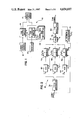
FIG. 1 is a block diagram of video signal apparatus incorporating the present invention;
FIG. 2 is a block diagram of the TDM record circuit of the apparatus FIG. 1;
FIG. 3 is a block diagram of the TDM playback circuit of the apparatus of FIG. 1;
FIG. 4 is a block diagram of the signal generator and TDM control circuit of the apparatus of FIG. 1;
FIG. 5A is an illustrative diagram of a TDM video signal;
FIG. 5B and FIG. 5C are respectively general and specific timing diagrams for the TDM signal of FIG. 5A;
FIG. 6 is a signal value versus time diagram of the horizontal segment of the signal of FIG. 5A; and
FIG. 7 is a diagram of a TDM buffer segment illustrating the present invention.
DESCRIPTION OF THE PREFERRED EMBODIMENT
Referring now to FIG. 1, there is shown apparatus incorporating the time-division- multiplex video signal processing technique of the present invention. As shown, apparatus 10 includes a video signal source 12 which may for example be a color video camera or a transmission source such as a broadcast, satellite or cable transmission system. In the following description, it will be assumed that source 12 supplies a standard NTSC composite color video signal used in the U.S. It will be appreciated, however that other composite video signal systems such as the PAL and SECAM systems used in other parts of the world may also be processed in accordance with the present invention. It will also be appreciated that source 12 may provide component video signals such as a YIQ component video signal or an RGB component video signal. The color video signal is supplied to a TDM record circuit 14 which converts the NTSC composite color video signal into a TDM video signal which is recorded on magnetic tape by means of magnetic tape assembly 16. Assembly 16 may, for example, be of a type used in consumer video cassette recorders. In such VCRs a rotating magnetic head or heads records the video signal in magnetic tracks that are slanted across the width of tape contained in a cassette.
Apparatus 10 also includes TDM playback circuit 18 which receives signals from magnetic tape assembly 16 and converts the TDM video signal to a composite color video signal or component color video signal which is applied to monitor 20 for display of video images. A signal generator and TDM control 22 is also provided for providing frequency signals and control signals to circuits 14 and 18.
It will be appreciated that video signal source 12, circuits 14, 18, assembly 16, and circuit 22 may be combined into a lightweight camera/recorder for use in recording still and movie type image sequences.
It will be also appreciated that TDM record and playback circuits 14 and 18, magnetic tape assembly 16, and control 22 may be combined into a single apparatus which functions as a video cassette recorder/player or that TDM playback circuit 18, magnetic tape assembly 16, and control 22 may be combined into a single apparatus which only plays back prerecorded video cassettes. Other combinations will be apparent to those skilled in the art including the combining of the TDM signal processing circuit of circuits 14 and 18 with conventional signal processing circuits as disclosed in commonly-assigned copending U.S. patent application Ser. No. 725,873, by Carl Schauffele, entitled VIDEO REPRODUCTION APPARATUS, filed Apr. 22, 1985.
Referring now to FIG. 2, there is shown in greater detail TDM record circuit 14 of the apparatus of FIG. 1. In general, the function of circuit 14 is to convert a composite color video signal in which the luminance and chrominance components occupy concurrent, overlapping frequency bandwidths into a time-division-multiplex video signal in which the luminance and chrominance components are separated and transmitted in time sequential manner in order to avoid time base errors, image degradation and color inaccuracies which may result if the composite video signal was recorded on magnetic tape.
As shown in FIG. 5A, the TDM signal has a horizontal line duration (which in the NTSC system is equal to approximately 63.5 msec). The TDM signal includes a series of segments which are processed in a time sequential manner. In FIG. 5A, TDM signal 24 includes H sync segment 26, compressed Q chrominance segment 28, first buffer segment 30, compressed I chrominance segment 32, second buffer segment 34, and compressed Y luminance segment 36. Referring to FIGS. 6 and 5B, it will be seen that H sync segment 26 includes a compressed horizontal sync portion 26A which has a duration from time t0 to t1 ; a black level portion 26B which has a duration from t1 to t2 and a chrominance level portion 26C which has a duration from time t2 to time t3.
Q chrominance segment 28 has a duration from time t3 to time t4, first buffer segment 30 has a duration from t4 to t5, I chrominance segment 32 has a duration from t5 to t6, second buffer segment 34 has a duration from t6 to t7, and Y luminance segment 36 has a duration from t7 to t8 (FIGS. 5A and 5B).
As shown in FIG. 2, TDM record circuit 14 receives a composite color video signal from source 12 (FIG. 1). This signal is applied to YIQ separator 38 which separates the I and Q chrominance components from the Y luminance component and may, for example, include a comb filter and chrominance demodulator (not shown). The separated Y, I and Q analog signal components are respectively applied to analog-to-digital converters (ADC) 40, 42, and 44. ADC 44 samples the Q chrominance analog signal at a frequency F1 and converts these analog samples to digital samples which are written into Q memory 46 at the F1 sampling frequency. The I analog chrominance component is sampled at a frequency F2 by ADC 42 and converted to digital samples which are stored in I memory 48 at the frequency of signal F2. Finally, the Y luminance analog signal is sampled by ADC 40 at a frequency F3 and converted to digital samples which are stored in Y memory 50 at the sampling frequency F3. Frequencies F1, F2, and F3 are chosen so as to be at least twice the highest frequency of each of the components sampled. As disclosed in the above described Schauffele U.S. patent application Ser. No. 725,873, the frequency F1 may for example be chosen to be 2.013 MHz.; frequency F2 may be chosen to have a frequency of 4.027 MHz and frequency F3 may be chosen to be 14.097 MHz.
In order to produce a time-division-multiplex color video signal according to the present invention, the I and Q chrominance components and Y luminance component are compressed in time and rearranged in a time sequential fashion. A sampling frequency F4 is chosen to effect production of the TDM signal during a single horizontal line period. Thus, frequency F4 may be chosen at 18.125 MHz and this frequency is sequentially applied to Q memory 46, I memory 48 and Y memory 50 to produce the TDM signal. Timing of the TDM signal is simplified by chosing the TDM sampling frequency F4 as a multiple of the horizontal frequency FH. In this case, F4 =1152 FH. Timing may be further simplified by making the durations of each of the TDM segments integrally divisible by the same number, in this case 9, so that timing may be effected by a slower, less costly, less complex timing circuit (see copending U.S. patent application Ser. No. 793,820, filed Nov 11, 1985, entitled APPARATUS FOR PROCESSING A TIME-DIVISION-MULTIPLEX VIDEO SIGNAL HAVING SEGMENT DURATIONS DIVISIBLE BY A COMMON NUMBER).
Signal generator and TDM control circuit 22 (FIG. 1) provides the timing for processing the TDM signal shown in FIG. 5A. As shown in FIG. 4, signal generator 52 (which may be of a type known to those skilled in the art) produces signals having frequencies F1, F2, F3, and F4. The F1, F2, and F3 signals are respectively supplied to circuit 14 and, as described above, signal F4 is also supplied to a divide by N circuit 54. In this example, N is 9 in order to produce a signal F5 having a frequency which is 1/9 of the frequency of F4. Since signal F4 has a frequency equal to 1152 FH, signal F5 has a frequency equal to 1/9 of F4 or 128 FH. The timing of TDM segments is effected by counting the periods of signal F5 by a seven-bit counter 56 having output terminals labeled "1", "2", " 4", "8", "16", "32", and "64". The output of these terminals are selectively applied to AND gates 58, 60, 62, 64, 66, 68, 70, and 72 to produce respective control signals C1, C2, C3, C4, C5, C6, C7, and C8.
With reference to FIGS. 5A, 5B, and 5C, production of the TDM video signal is initiated at a suitable time t0 which corresponds to the delayed leading edge of the horizontal sync pulse of the composite video signal. The TDM signal is applied to an output transmission path 78 such as wire, cable or the like. At time t0, counter 56 begins counting pulses of frequency F5, and H segment processor 74 initiates the production of segment 26. From time t0 to time t1 (count 0 to count 2), compressed sync portion 26A is produced; from time t1 to t2 (count 2 to count 4) black level portion 26B is produced; and from t2 to t3, (count 4 to count 6) chrominance level portion 26C is produced. Timing is effected by the control signals C1, C2 and C3 applied to processor 74.
At time t3 (count 6) control signal C3 is also applied to Q memory 46 (FIG. 2) to initiate formation of Q segment 28 by reading out digital samples of the Q chrominance component at the time-compression sampling frequency F4. DAC 76 converts the digital samples to analog samples and applies them in series to output path 76.
According to the present invention, a buffer segment 30 is formed between segments 28 and 32 in order to isolate these segments and to allow the TDM signal to change to an appropriate value to compensate for the response time of transmission path 78. If the response to large changes in signal value is insufficient, the first samples of the next TDM component segment may be distorted, resulting in image degradation and color inaccuracies in a reproduced image. The formation of buffer segment 30 is illustrated in FIG. 7. As shown, the last samples Qn-2, Qn-1, Qn of Q segment 28 are separated by buffer segment 30 from the first samples I1, I2, I3, of I segment 32. FIG. 7 shows the signal values of the Q and I samples to be have voltage levels which would be produced after the digital signals read out of memories 46 and 48 (FIG. 2) are converted to analog signals by digital to analog converter (DAC) 76. After production of the last sample Qn, production of the first sample I, is delayed from t4 to t5 while the buffer segment 30 is formed. During the buffer period, the signal value of the first I segment sample (I1) is applied to transmission path 78 to cause the value of the TDM signal (dashed line 31) to change from the value of sample Qn to the value of sample I1. Thus, during the time t4 to t5, the value (voltage) of the first sample I1 is applied to path 78 without the actual production of this sample. The duration of buffer segment 30 is nine periods of signal F4 or one period of signal F5.
At time t5, control signal C5 terminates buffer segment 30 and initiates reading out of samples from I memory 48 to produce I segment 32. At time t6 control signal C6 terminates the reading out of samples from I memory 48 and applies the value of the first sample of the Y luminance signal to output path 78 during the duration of buffer segment 34. At time t7, control signal C7 initiates the reading out of Y samples from Y memory 50 to produce segment 36.
The TDM signal is modulated onto an FM carrier by FM modulator 80 (see FIG. 2) and the FM signal supplied to magnetic tape assembly 16 to be recorded on magnetic tape.
Referring now to FIG. 3, there is shown in greater detail TDM playback circuit 18. As shown, a TDM signal played back from magnetic tape by assembly 16 is supplied to FM demodulator 82 which demodulates the TDM signal. The first segment 26 of the TDM signal is applied to H sync processor 84 which samples the sync, black and chrominance levels of segment portions 26A, 26B, and 26C and produces a composite horizontal sync and blanking signal at an appropriate time. The chrominance level signal is also used to control the level of the I and Q chrominance components by means not shown. At time t3, the Q chrominance segment 28 is sampled by analog-to-digital converter (ADC) 86 at the sampling frequency F4 and written into Q memory 88. At t4, the writing in of Q samples into memory 88 is terminated and during buffer segment 30 the transmission path 83 stabilizes. At t5, control signal C5 initiates reading into I memory 90, samples of I segment 32 at the frequency sampling rate of F4. Reading into I memory is terminated at time t6 by control signal C6. Samples of Y segment 36 produced by ADC 86 are written into Y memory 92 from t7 to t8.
After an appropriate delay to allow reading into memories 88, 90, and 92 of the respective Q, I and Y samples, H sync processor 84 produces a composite horizontal sync and blanking signal which is applied to composite video processing circuit 94. At the start of the active video portion of the composite video signal, there is simultaneously read out from memories 88, 90, and 92 respective Q digital samples at frequency F1, I digital samples at frequency F2, and Y digital samples at frequency F3. The respective digital samples are converted by digital to analog converters (DAC) 96, 98, and 100 into appropriate Q chrominance, I chrominance and Y luminance signals which are applied to composite video signal processing circuit 94 to produce a composite NTSC color video signal which is applied to monitor 20.
The invention has been described in detail with particular reference to preferred embodiments thereof, but it will be understood that variations and modifications can be effected within the spirit and scope of the invention.

Claims (6)

What is claimed is:
1. Video signal apparatus comprising:
an output transmission path;
circuit means for providing to said transmission path a time-division-multiplex (TDM) video signal having a first compressed segment including a series of time-compressed samples of varying signal value representing one of two components of a video signal and a second compressed segment, sequential in time to said first compressed segment, said second segment including a series of time-compressed samples of varying signal value representing the other of said two components of said video signal; and
control means for controlling said circuit means to form a buffer segment between said first and second compressed segments such that during said buffer segment, the signal value of the TDM signal is caused to change from the value of the last sample of said first segment to the value of the first sample of said second segment by applying to the output transmission path, during said buffer segment, the signal value of the first sample of said second segment.
2. The apparatus of claim 1 wherein said samples of said first compressed segment represent one of the chrominance and luminance components of a color video signal and have varying signal voltages, wherein said samples of said second compressed segment represent the other of the chrominance and luminance components of said color video signal and have varying signal voltages and wherein during said buffer segment, the voltage of the first sample of said second compressed segment is applied to said output transmission path.
3. Video signal apparatus comprising:
an output transmission path;
circuit means, coupled to said output transmission path, for processing a color video signal having a luminance component and two chrominance components to produce a time-division-multiplex (TDM) video signal having (1) a first compressed segment including a series of time-compressed samples of varying signal value representing one of said luminance and said two chrominance components of said color video signal; (2) a second compressed segment including a series of time compressed samples of varying signal value representing another of said luminance and said two chrominance components of said color video signal; and (3) a third compressed segment including a series of time compressed samples of varying signal value representing the last of said luminance and said two chrominance components of said color video signal; and
control means for controlling said circuit means (1) to form a buffer segment between said first and second compressed segments such that during said buffer segment, the signal value of said TDM signal is caused to change from the value of the last sample of said first segment to the value of the first sample of said second segment by applying to the output transmission path the signal value of the first sample of said second segment, and (2) to form a buffer segment between said second and third compressed segments such that during said buffer segment, the signal value of said TDM signal is caused to change from the value of the last sample of said second segment to the value of the first sample of the third segment by applying to the output transmission path the signal value of the first sample of said third segment.
4. The apparatus of claim 3 wherein the varying signal values of said samples of said first second and third compressed segments are varying signal voltage values, wherein, during said buffer segment between said first and second compressed segments, the voltage of the first sample of said second segment is applied to said output transmission path, and wherein, during said buffer segment between said second and third compressed segments, the voltage of the first sample of said third segment is applied to said output transmission path.
5. The apparatus of claim 3 including means for recording said TDM video signal on recording media.
6. The apparatus of claim 5 wherein said recording means is a magnetic tape recorder and wherein said TDM video signal is recorded on magnetic tape.
US06/793,810 1985-11-01 1985-11-01 Video signal apparatus for processing a time-division-multiplex video signal having a buffer segment Expired - Fee Related US4654697A (en)

Priority Applications (1)

Application Number Priority Date Filing Date Title
US06/793,810 US4654697A (en) 1985-11-01 1985-11-01 Video signal apparatus for processing a time-division-multiplex video signal having a buffer segment

Applications Claiming Priority (1)

Application Number Priority Date Filing Date Title
US06/793,810 US4654697A (en) 1985-11-01 1985-11-01 Video signal apparatus for processing a time-division-multiplex video signal having a buffer segment

Publications (1)

Publication Number Publication Date
US4654697A true US4654697A (en) 1987-03-31

Family

ID=25160861

Family Applications (1)

Application Number Title Priority Date Filing Date
US06/793,810 Expired - Fee Related US4654697A (en) 1985-11-01 1985-11-01 Video signal apparatus for processing a time-division-multiplex video signal having a buffer segment

Country Status (1)

Country Link
US (1) US4654697A (en)

Cited By (5)

* Cited by examiner, † Cited by third party
Publication number Priority date Publication date Assignee Title
US4752830A (en) * 1986-09-29 1988-06-21 Eastman Kodak Company Time division multiplex video recorder with enhanced vertical chrominance sampling rate
DE4120317A1 (en) * 1990-06-27 1992-01-09 Samsung Electronics Co Ltd CIRCUIT FOR PLAYING DIGITAL IMAGE SIGNALS
US5244519A (en) * 1987-11-12 1993-09-14 Angli Holding B.V. Coating material for and method of inhibiting pathogenic and saprophitic organisms
US20020013948A1 (en) * 2000-03-13 2002-01-31 Erwin Aguayo Video data management, transmission, and control system and method emloying distributed video segments microcasting
US20140169479A1 (en) * 2012-02-28 2014-06-19 Panasonic Corporation Image processing apparatus and image processing method

Citations (6)

* Cited by examiner, † Cited by third party
Publication number Priority date Publication date Assignee Title
US4001883A (en) * 1974-03-07 1977-01-04 Honeywell Information Systems, Inc. High density data storage on magnetic disk
US4015286A (en) * 1975-01-23 1977-03-29 Eli S. Jacobs Digital color television system
US4084181A (en) * 1976-01-21 1978-04-11 Hitachi, Ltd. Apparatus for transmission of chrominance signals during blanking period
US4240102A (en) * 1978-03-16 1980-12-16 Rca Corporation Identification system for SECAM or SECAM/PAL color television receivers
US4335393A (en) * 1980-04-15 1982-06-15 Harris Video Systems, Inc. Method and system using sequentially encoded color and luminance processing of video type signals to improve picture quality
US4473850A (en) * 1980-08-08 1984-09-25 Robert Bosch Gmbh Method and apparatus for recording digitally coded television signals

Patent Citations (6)

* Cited by examiner, † Cited by third party
Publication number Priority date Publication date Assignee Title
US4001883A (en) * 1974-03-07 1977-01-04 Honeywell Information Systems, Inc. High density data storage on magnetic disk
US4015286A (en) * 1975-01-23 1977-03-29 Eli S. Jacobs Digital color television system
US4084181A (en) * 1976-01-21 1978-04-11 Hitachi, Ltd. Apparatus for transmission of chrominance signals during blanking period
US4240102A (en) * 1978-03-16 1980-12-16 Rca Corporation Identification system for SECAM or SECAM/PAL color television receivers
US4335393A (en) * 1980-04-15 1982-06-15 Harris Video Systems, Inc. Method and system using sequentially encoded color and luminance processing of video type signals to improve picture quality
US4473850A (en) * 1980-08-08 1984-09-25 Robert Bosch Gmbh Method and apparatus for recording digitally coded television signals

Non-Patent Citations (2)

* Cited by examiner, † Cited by third party
Title
Electronics, 7/14/83 pp. 82 83. *
Electronics, 7/14/83--pp. 82-83.

Cited By (7)

* Cited by examiner, † Cited by third party
Publication number Priority date Publication date Assignee Title
US4752830A (en) * 1986-09-29 1988-06-21 Eastman Kodak Company Time division multiplex video recorder with enhanced vertical chrominance sampling rate
US5244519A (en) * 1987-11-12 1993-09-14 Angli Holding B.V. Coating material for and method of inhibiting pathogenic and saprophitic organisms
DE4120317A1 (en) * 1990-06-27 1992-01-09 Samsung Electronics Co Ltd CIRCUIT FOR PLAYING DIGITAL IMAGE SIGNALS
US5191437A (en) * 1990-06-27 1993-03-02 Samsung Electronics Co., Ltd. Digital image signal playback circuit for combining two channel parallel picture data into a single channel
US20020013948A1 (en) * 2000-03-13 2002-01-31 Erwin Aguayo Video data management, transmission, and control system and method emloying distributed video segments microcasting
US20140169479A1 (en) * 2012-02-28 2014-06-19 Panasonic Corporation Image processing apparatus and image processing method
US9723308B2 (en) * 2012-02-28 2017-08-01 Panasonic Intellectual Property Management Co., Ltd. Image processing apparatus and image processing method

Similar Documents

Publication Publication Date Title
US4910605A (en) Video signal recording method and apparatus for field-segment recording
US4376957A (en) Transmission system with sequential time-compressed baseband color
JPH0467396B2 (en)
JPS623637B2 (en)
US4691245A (en) Method and apparatus for combining two color video signals
US4654697A (en) Video signal apparatus for processing a time-division-multiplex video signal having a buffer segment
US4686582A (en) Head switching in high resolution video reproduction apparatus
US4752839A (en) Head switching in high resolution video reproduction apparatus
KR900008454B1 (en) Picture signal recording method and recording/play back apparatus
US4580173A (en) Transmission system with sequential time-compressed baseband color
KR920007918B1 (en) Recording and playback apparatus of television signal
US4739419A (en) Apparatus for eliminating midfield skew error by delaying the lower half field of a T M format video signal to be recorded on the second of two tracks
EP0486300B1 (en) Video signal processing apparatus
US4695874A (en) Apparatus for processing a time-division multiplex video signal having signal durations divisible by the same number
JP3010742B2 (en) Rotating head type magnetic recording / reproducing device
KR910004286B1 (en) Transmission recording and play back method of color television signal
Machida et al. Simplified television standards converter as a video tape reproduction system
Itoga et al. Wideband recording technology for high-definition baseband VCRs
JP3066214B2 (en) Magnetic recording / reproducing device
JP2911145B2 (en) Video tape recorder
JP2959329B2 (en) Video signal recording method
JPH0430238B2 (en)
JP2915441B2 (en) Video playback apparatus and method
JPH0530355B2 (en)
JPS6359281A (en) Television signal recording and reproducing device

Legal Events

Date Code Title Description
AS Assignment

Owner name: EASTMAN KODAK COMPANY, ROCHESTER, NEW YORK, A NEW

Free format text: ASSIGNMENT OF ASSIGNORS INTEREST.;ASSIGNOR:SASSON, STEVEN J.;REEL/FRAME:004649/0236

Effective date: 19851028

Owner name: EASTMAN KODAK COMPANY, A NEW JERSEY CORP.,NEW YORK

Free format text: ASSIGNMENT OF ASSIGNORS INTEREST;ASSIGNOR:SASSON, STEVEN J.;REEL/FRAME:004649/0236

Effective date: 19851028

FEPP Fee payment procedure

Free format text: PAYOR NUMBER ASSIGNED (ORIGINAL EVENT CODE: ASPN); ENTITY STATUS OF PATENT OWNER: LARGE ENTITY

FPAY Fee payment

Year of fee payment: 4

REMI Maintenance fee reminder mailed
LAPS Lapse for failure to pay maintenance fees
FP Lapsed due to failure to pay maintenance fee

Effective date: 19950405

STCH Information on status: patent discontinuation

Free format text: PATENT EXPIRED DUE TO NONPAYMENT OF MAINTENANCE FEES UNDER 37 CFR 1.362