US4654599A - Four phase clock signal generator - Google Patents
Four phase clock signal generator Download PDFInfo
- Publication number
- US4654599A US4654599A US06/751,718 US75171885A US4654599A US 4654599 A US4654599 A US 4654599A US 75171885 A US75171885 A US 75171885A US 4654599 A US4654599 A US 4654599A
- Authority
- US
- United States
- Prior art keywords
- shift register
- input
- signal
- clock signal
- clear
- Prior art date
- Legal status (The legal status is an assumption and is not a legal conclusion. Google has not performed a legal analysis and makes no representation as to the accuracy of the status listed.)
- Expired - Lifetime
Links
Images

Classifications
-
- H—ELECTRICITY
- H03—ELECTRONIC CIRCUITRY
- H03K—PULSE TECHNIQUE
- H03K5/00—Manipulating of pulses not covered by one of the other main groups of this subclass
- H03K5/15—Arrangements in which pulses are delivered at different times at several outputs, i.e. pulse distributors
- H03K5/15013—Arrangements in which pulses are delivered at different times at several outputs, i.e. pulse distributors with more than two outputs
- H03K5/1506—Arrangements in which pulses are delivered at different times at several outputs, i.e. pulse distributors with more than two outputs with parallel driven output stages; with synchronously driven series connected output stages
- H03K5/15093—Arrangements in which pulses are delivered at different times at several outputs, i.e. pulse distributors with more than two outputs with parallel driven output stages; with synchronously driven series connected output stages using devices arranged in a shift register
Definitions
- the present invention relates to the field of electronic digital computer systems and in particular to a generator of a multiple phase clocking signal that is comprised of high frequency, uniformally spaced, uniformally shaped, pulses that are utilized for timing and synchronizing the operation of a computer system.
- the pulses of the clock phase signal In addition to the time relationship between the occurrence of the pulses of the clock phase signal, it is common for the pulses of the clock phase signal to be of similar signal shape with regard to rise time, fall time and amplitude.
- the clock phase signals are utilized through their known shape and time relationships to time sequences of computer system operation. If the clock phase signal generating circuitry fails to maintain the predetermined time relationship, a so-called clock skew results, and if this skew is too great, the computer system will generate error signals that stop computer system operation.
- clocking rate requirements are a function of the switching speed of the circuitry incorporated in the equipment. While early vacuum tube circuitry required clocking rate capability in the range of hundreds of kilohertz (KHz), discrete semiconductor circuits have required clocking rates that are orders of magnitude faster, while very large scale integrated (VLSI) circuitry have required clocking rates that are orders of magnitude greater than discrete semiconductor circuits. As clock rates increase, tolerances within the clock phase signal are necessarily diminished, and clock skew becomes an ever increasing problem.
- a major problem is that a flip-flop circuit will not exhibit the precisely same switching rates for driving an output terminal to achieve a rising edge as it will to drive the output terminal in the opposite direction to achieve a falling edge. At high clocking rates these differences in circuit switching rates result in an output clock signal waveform that does not exhibit the characteristic of a 50 percent duty cycle with an acceptable tolerance, and, accordingly, provides an unsatisfactory operation of the controlled circuitry.
- flip-flop dividers may work adequately, but would not be self-adjusting, would be relatively expensive, and would not yield an operation of a fixed pulse width, plus or minus 1 nanosecond (ns) which is nominally 50% duty cycle at normal operating frequency.
- ns nanosecond
- a further drawback is that to obtain symmetrical clocking signals using this flip-flop technique it requires clock source signal frequencies double the desired output frequency. If the clock source signal circuitry is to be fabricated utilizing the same circuit technology as does the logic circuitry that is to be gated, the flip-flop divider approach is unworkable at higher frequencies.
- a multiphase clock signal always starts or begins with the first phase .0.1 pulse without the generation of runt or distorted signals.
- the clock generating circuitry of the present invention ensures that the multiphase clock signal always starts with the first phase .0.1 pulse while using the same semiconductor technology and requiring no adjustments of timing or of pulse shape. It is particularly adapted for high volume production of high speed, low to medium scale, computer systems, such as personal computers, while operating at a frequency that is near the speed limit of the logic family that is incorporated in the associated computer system.
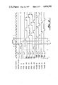
- FIG. 2 is an illustration of a timing diagram associated with the operation of the system of FIG. 1.
- Shift register 22 is a 4-bit bidirectional shift register with data inputs P0, P1, P2, P3 and data outputs Q0, Q1, Q2, Q3. Data transfer or shifting within shift register 22 occurs only on the positive going edge of clock signal 32 at the CP input. For the illustrated shift right operation, input S0 is held Hi, input S1 is held Lo, and for parallel load of the P0, P1, P2, P3 data inputs, both S0, S1 are held Hi.
- Pulse generators 24, 26, 28, 30 are enabled by Hi inputs from the Q outputs of shift register 22, but such Hi inputs produce the four phase clock signal Lo output pulses on lines 25, 27, 29, 31 only on the positive going edge of clock signal 32 from line 17 (and oscillator 12).
- Oscillator 12 is running and coupling the 37 MHz clock signal 32 of FIG. 2 to line 13;
- Oscillator 12 is running and coupling clock signal 32 to NAND 14;
- NAND 14 on line 15 is the complement, or inverse, of clock signal 32;
- NAND 16 On line 17 is the same as clock signal 32;
- the first positive going edge of clock signal 32 after time t0, as at time t1, at pulse generators 24, 26, 28, 30, via line 17, will enable the unknown outputs Q0, Q1, Q2, Q3 of shift register 22 to be coupled to the respectively associated output lines 25, 27, 29, 31, respectively, as the four phases .0.1, .0.2, .0.3, .0.4 of the four phase clock signal output of multiphase clock signal generator 10.
- This enabling of the unknown states of the outputs Q0, Q1, Q2, Q3 of shift register 22 to be coupled to the four phase signal output lines 25, 27, 29, 31 after the occurrence of the first positive going edge of clock signal 32 after Power On will be the only time that random four phase clock signals will be output from four phase clock signal generator 10.
- FF 18 With the Master Clear signal, represented by timing signal 42 of FIG. 2, on line 40 being held Lo, FF 18 will be forced into a Clear condition whereby the Q output, represented by timing signal 44, is held Lo, holding, via line 46, the P0 input of shift register 22 Lo while the Q output, via line 48, forces FF 20 into a Clear condition.
- both inputs S0 and S1 of shift register 22 are held Hi whereby shift register 22 will now accept parallel data on its inputs P0, P1, P2, P3, which inputs are now being held Lo via line 46 and line 50, which is coupled to a ground voltage source.
- Master Clear signal 42 on line 40 switches to and is held in its Hi state, as at time t3, which Hi state is clocked into FF 18, via line 17 upon the next positive going edge of clock signal 32, as at time t4.
- clock signal 32 at shift register 22 input CP, will also go Hi; however, all data inputs P0, P1, P2, P3 are held Lo and operating mode inputs S0, S1 are still held Hi.
- the delay ⁇ of FF 18 delays the change of state of FF 18 output Q, until time t5 and prevents this positive going edge of clock signal 32 from loading any new data into shift register 22.
- the new data which is a Hi input to P0 and Lo inputs to P1, P2, P3, is clocked into shift register 22.
- new Hi data is clocked into FF20, the Q output of which goes Lo, after the propagation delay of FF20, and, via line 54, the operating mode input S1 goes Lo setting shift register 22 into a right serial shift mode. Shift register 22 is parallel loaded before the Q output of FF20 goes Lo.
- phase .0.1 of the four phase clock signal is enabled; however, because pulse generators 24, 26, 28, 30 are positive edge triggered, no four phase pulse signals have yet been generated.
- the first pulse, phase .0.1, represented by timing signal 70, will be generated on the next positive going edge of clock signal 32, as at time t7.
- the single active signal established in stage 1 of shift register 22 will be shifted through shift register 22, as represented by timing signals 60, 62, 64, 66, at the frequency of clock signal 32 to be reset into the first stage of shift register 22 via output Q3, line 59 and input DSR. This operation is as indicated by FIG. 2.
- the output from the four phase clock signal generator 10 will stop on the next phase or the following phase .0.1, .0.2, .0.3, or .0.4 dependent upon the timing of the Master Clear signal.
- Signal generator 10 will not necessarily stop only after output of phase .0.4; however, because a Master Clear signal has been initiated, such random stopping of the four phase clock signal from four phase clock signal generator 10 is not a problem.
- the start-up after the coupling of a Hi Master Clear signal to line 40 will be as described above.
- Four phase clock signal generator 10 includes provisions for operation in a Maintenance Mode with an external oscillator of any frequency from 0 to 37 Megahertz.
- a change from normal operation utilizing oscillator 12 to Maintenance Mode operation utilizing an external oscillator must be performed under precise conditions.
- Maintenance Mode signal on line 38 must be switched to be held Lo prior to the coupling of a Hi Master Clear signal to line 40 and several four phase clock signal pulses .0.1, .0.2, .0.3, .0.4 must be generated before the Master Clear signal is switched Hi to set up shift register 22 for the correct initial states.
- This Maintenance Mode condition would require one Hi to Lo transition of the external oscillator signal on line 36 while the Master Clear signal on line 40 would be switched Hi prior to the next negative going edge of the external oscillator signal on line 36.
- the first phase signal .0.1 will be coupled to line 25 on the next negative going transition of the external oscillator signal on line 36.
- Successive phases, .0.2, .0.3, .0.4, .0.1, .0.2, .0.3, .0.4, .0.1, etc., as represented by timing signals 70, 72, 74, 76, will follow in sequence.
Abstract
Description
Claims (3)
Priority Applications (1)
| Application Number | Priority Date | Filing Date | Title |
|---|---|---|---|
| US06/751,718 US4654599A (en) | 1985-07-05 | 1985-07-05 | Four phase clock signal generator |
Applications Claiming Priority (1)
| Application Number | Priority Date | Filing Date | Title |
|---|---|---|---|
| US06/751,718 US4654599A (en) | 1985-07-05 | 1985-07-05 | Four phase clock signal generator |
Publications (1)
| Publication Number | Publication Date |
|---|---|
| US4654599A true US4654599A (en) | 1987-03-31 |
Family
ID=25023185
Family Applications (1)
| Application Number | Title | Priority Date | Filing Date |
|---|---|---|---|
| US06/751,718 Expired - Lifetime US4654599A (en) | 1985-07-05 | 1985-07-05 | Four phase clock signal generator |
Country Status (1)
| Country | Link |
|---|---|
| US (1) | US4654599A (en) |
Cited By (8)
| Publication number | Priority date | Publication date | Assignee | Title |
|---|---|---|---|---|
| US4877974A (en) * | 1987-12-04 | 1989-10-31 | Mitsubishi Denki Kabushiki Kaisha | Clock generator which generates a non-overlap clock having fixed pulse width and changeable frequency |
| US5053639A (en) * | 1989-06-16 | 1991-10-01 | Ncr Corporation | Symmetrical clock generator and method |
| US5394443A (en) * | 1993-12-23 | 1995-02-28 | Unisys Corporation | Multiple interval single phase clock |
| US5440250A (en) * | 1993-06-26 | 1995-08-08 | Deutsche Itt Industries Gmbh | Clock-generating circuit for clock-controlled logic circuits |
| US5517147A (en) * | 1994-11-17 | 1996-05-14 | Unisys Corporation | Multiple-phase clock signal generator for integrated circuits, comprising PLL, counter, and logic circuits |
| US6239627B1 (en) * | 1995-01-03 | 2001-05-29 | Via-Cyrix, Inc. | Clock multiplier using nonoverlapping clock pulses for waveform generation |
| KR100347147B1 (en) * | 2000-09-23 | 2002-08-03 | 주식회사 하이닉스반도체 | Circuit for generating clock |
| US10340904B2 (en) | 2016-06-28 | 2019-07-02 | Altera Corporation | Method and apparatus for phase-aligned 2X frequency clock generation |
Citations (3)
| Publication number | Priority date | Publication date | Assignee | Title |
|---|---|---|---|---|
| US3740660A (en) * | 1971-05-27 | 1973-06-19 | North American Rockwell | Multiple phase clock generator circuit with control circuit |
| US4386323A (en) * | 1980-01-31 | 1983-05-31 | U.S. Philips Corporation | Arrangement for synchronizing the phase of a local clock signal with an input signal |
| US4443765A (en) * | 1981-09-18 | 1984-04-17 | The United States Of America As Represented By The Secretary Of The Navy | Digital multi-tapped delay line with automatic time-domain programming |
-
1985
- 1985-07-05 US US06/751,718 patent/US4654599A/en not_active Expired - Lifetime
Patent Citations (3)
| Publication number | Priority date | Publication date | Assignee | Title |
|---|---|---|---|---|
| US3740660A (en) * | 1971-05-27 | 1973-06-19 | North American Rockwell | Multiple phase clock generator circuit with control circuit |
| US4386323A (en) * | 1980-01-31 | 1983-05-31 | U.S. Philips Corporation | Arrangement for synchronizing the phase of a local clock signal with an input signal |
| US4443765A (en) * | 1981-09-18 | 1984-04-17 | The United States Of America As Represented By The Secretary Of The Navy | Digital multi-tapped delay line with automatic time-domain programming |
Cited By (8)
| Publication number | Priority date | Publication date | Assignee | Title |
|---|---|---|---|---|
| US4877974A (en) * | 1987-12-04 | 1989-10-31 | Mitsubishi Denki Kabushiki Kaisha | Clock generator which generates a non-overlap clock having fixed pulse width and changeable frequency |
| US5053639A (en) * | 1989-06-16 | 1991-10-01 | Ncr Corporation | Symmetrical clock generator and method |
| US5440250A (en) * | 1993-06-26 | 1995-08-08 | Deutsche Itt Industries Gmbh | Clock-generating circuit for clock-controlled logic circuits |
| US5394443A (en) * | 1993-12-23 | 1995-02-28 | Unisys Corporation | Multiple interval single phase clock |
| US5517147A (en) * | 1994-11-17 | 1996-05-14 | Unisys Corporation | Multiple-phase clock signal generator for integrated circuits, comprising PLL, counter, and logic circuits |
| US6239627B1 (en) * | 1995-01-03 | 2001-05-29 | Via-Cyrix, Inc. | Clock multiplier using nonoverlapping clock pulses for waveform generation |
| KR100347147B1 (en) * | 2000-09-23 | 2002-08-03 | 주식회사 하이닉스반도체 | Circuit for generating clock |
| US10340904B2 (en) | 2016-06-28 | 2019-07-02 | Altera Corporation | Method and apparatus for phase-aligned 2X frequency clock generation |
Similar Documents
| Publication | Publication Date | Title |
|---|---|---|
| US5914996A (en) | Multiple clock frequency divider with fifty percent duty cycle output | |
| US5204555A (en) | Logic array having high frequency internal clocking | |
| US5388249A (en) | Data processing system generating clock signal from an input clock, phase locked to the input clock and used for clocking logic devices | |
| US5623223A (en) | Glitchless clock switching circuit | |
| US5315181A (en) | Circuit for synchronous, glitch-free clock switching | |
| JP2758994B2 (en) | Tuning ring oscillator circuit | |
| US6242953B1 (en) | Multiplexed synchronization circuits for switching frequency synthesized signals | |
| JPH04217115A (en) | Integrated circuit for changing relation in phase between at least one clock phase output and reference clock | |
| US5517147A (en) | Multiple-phase clock signal generator for integrated circuits, comprising PLL, counter, and logic circuits | |
| US5230013A (en) | PLL-based precision phase shifting at CMOS levels | |
| JP3426608B2 (en) | Clock deskew circuit | |
| US5794019A (en) | Processor with free running clock with momentary synchronization to subsystem clock during data transfers | |
| US4654599A (en) | Four phase clock signal generator | |
| US4703495A (en) | High speed frequency divide-by-5 circuit | |
| JP2579237B2 (en) | State element circuit having a flow-through latch circuit, VLSI circuit having the state element circuit, and method of operating a latch as a functional alternative to a master-slave flip-flop | |
| WO1999004528A1 (en) | A method and apparatus for synchronizing a control signal | |
| US4988892A (en) | Method and circuit for generating dependent clock signals | |
| US5668982A (en) | System and method for using a half-clock module to implement computer timing control circuitry | |
| CN110011643B (en) | Synchronous ring oscillator and method for synchronizing same | |
| US6249157B1 (en) | Synchronous frequency dividing circuit | |
| EP0847140B1 (en) | A circuit and method for generating clock signals | |
| US5801568A (en) | Precise delay line circuit with predetermined reset time limit | |
| US4977581A (en) | Multiple frequency clock system | |
| JP2000232339A (en) | Flip-flop circuit with clock signal controlling function and clock control circuit | |
| US7049864B2 (en) | Apparatus and method for high frequency state machine divider with low power consumption |
Legal Events
| Date | Code | Title | Description |
|---|---|---|---|
| AS | Assignment |
Owner name: SPERRY CORPORATION, 1290 AVE. OF THE AMERICAS, NEW Free format text: ASSIGNMENT OF ASSIGNORS INTEREST.;ASSIGNORS:ZBINDEN, TERRY B.;MARTHALER, RICHARD D.;REEL/FRAME:004945/0067 Effective date: 19850628 Owner name: SPERRY CORPORATION, A CORP. OF DE,NEW YORK Free format text: ASSIGNMENT OF ASSIGNORS INTEREST;ASSIGNORS:ZBINDEN, TERRY B.;MARTHALER, RICHARD D.;REEL/FRAME:004945/0067 Effective date: 19850628 |
|
| STCF | Information on status: patent grant |
Free format text: PATENTED CASE |
|
| AS | Assignment |
Owner name: SPERRY CORPORATION, 1290 AVENUE OF THE AMERICAS, N Free format text: ASSIGNMENT OF ASSIGNORS INTEREST.;ASSIGNORS:ZBINDEN, TERRY B.;MARTHALER, RICHARD D.;REEL/FRAME:004725/0761 Effective date: 19850628 |
|
| FPAY | Fee payment |
Year of fee payment: 4 |
|
| FEPP | Fee payment procedure |
Free format text: PAYOR NUMBER ASSIGNED (ORIGINAL EVENT CODE: ASPN); ENTITY STATUS OF PATENT OWNER: LARGE ENTITY |
|
| FPAY | Fee payment |
Year of fee payment: 8 |
|
| FPAY | Fee payment |
Year of fee payment: 12 |