US4641426A - Surface mount compatible connector system with mechanical integrity - Google Patents
Surface mount compatible connector system with mechanical integrity Download PDFInfo
- Publication number
- US4641426A US4641426A US06/747,343 US74734385A US4641426A US 4641426 A US4641426 A US 4641426A US 74734385 A US74734385 A US 74734385A US 4641426 A US4641426 A US 4641426A
- Authority
- US
- United States
- Prior art keywords
- component
- contacts
- printed circuit
- circuit board
- holes
- Prior art date
- Legal status (The legal status is an assumption and is not a legal conclusion. Google has not performed a legal analysis and makes no representation as to the accuracy of the status listed.)
- Expired - Fee Related
Links
Images

Classifications
-
- H—ELECTRICITY
- H05—ELECTRIC TECHNIQUES NOT OTHERWISE PROVIDED FOR
- H05K—PRINTED CIRCUITS; CASINGS OR CONSTRUCTIONAL DETAILS OF ELECTRIC APPARATUS; MANUFACTURE OF ASSEMBLAGES OF ELECTRICAL COMPONENTS
- H05K3/00—Apparatus or processes for manufacturing printed circuits
- H05K3/30—Assembling printed circuits with electric components, e.g. with resistor
- H05K3/32—Assembling printed circuits with electric components, e.g. with resistor electrically connecting electric components or wires to printed circuits
- H05K3/34—Assembling printed circuits with electric components, e.g. with resistor electrically connecting electric components or wires to printed circuits by soldering
- H05K3/3447—Lead-in-hole components
-
- H—ELECTRICITY
- H01—ELECTRIC ELEMENTS
- H01R—ELECTRICALLY-CONDUCTIVE CONNECTIONS; STRUCTURAL ASSOCIATIONS OF A PLURALITY OF MUTUALLY-INSULATED ELECTRICAL CONNECTING ELEMENTS; COUPLING DEVICES; CURRENT COLLECTORS
- H01R12/00—Structural associations of a plurality of mutually-insulated electrical connecting elements, specially adapted for printed circuits, e.g. printed circuit boards [PCB], flat or ribbon cables, or like generally planar structures, e.g. terminal strips, terminal blocks; Coupling devices specially adapted for printed circuits, flat or ribbon cables, or like generally planar structures; Terminals specially adapted for contact with, or insertion into, printed circuits, flat or ribbon cables, or like generally planar structures
- H01R12/50—Fixed connections
- H01R12/51—Fixed connections for rigid printed circuits or like structures
- H01R12/55—Fixed connections for rigid printed circuits or like structures characterised by the terminals
- H01R12/58—Fixed connections for rigid printed circuits or like structures characterised by the terminals terminals for insertion into holes
-
- H—ELECTRICITY
- H05—ELECTRIC TECHNIQUES NOT OTHERWISE PROVIDED FOR
- H05K—PRINTED CIRCUITS; CASINGS OR CONSTRUCTIONAL DETAILS OF ELECTRIC APPARATUS; MANUFACTURE OF ASSEMBLAGES OF ELECTRICAL COMPONENTS
- H05K2201/00—Indexing scheme relating to printed circuits covered by H05K1/00
- H05K2201/09—Shape and layout
- H05K2201/09009—Substrate related
- H05K2201/09036—Recesses or grooves in insulating substrate
-
- H—ELECTRICITY
- H05—ELECTRIC TECHNIQUES NOT OTHERWISE PROVIDED FOR
- H05K—PRINTED CIRCUITS; CASINGS OR CONSTRUCTIONAL DETAILS OF ELECTRIC APPARATUS; MANUFACTURE OF ASSEMBLAGES OF ELECTRICAL COMPONENTS
- H05K2201/00—Indexing scheme relating to printed circuits covered by H05K1/00
- H05K2201/10—Details of components or other objects attached to or integrated in a printed circuit board
- H05K2201/10007—Types of components
- H05K2201/10189—Non-printed connector
-
- H—ELECTRICITY
- H05—ELECTRIC TECHNIQUES NOT OTHERWISE PROVIDED FOR
- H05K—PRINTED CIRCUITS; CASINGS OR CONSTRUCTIONAL DETAILS OF ELECTRIC APPARATUS; MANUFACTURE OF ASSEMBLAGES OF ELECTRICAL COMPONENTS
- H05K2201/00—Indexing scheme relating to printed circuits covered by H05K1/00
- H05K2201/10—Details of components or other objects attached to or integrated in a printed circuit board
- H05K2201/10227—Other objects, e.g. metallic pieces
- H05K2201/10295—Metallic connector elements partly mounted in a hole of the PCB
- H05K2201/10303—Pin-in-hole mounted pins
-
- H—ELECTRICITY
- H05—ELECTRIC TECHNIQUES NOT OTHERWISE PROVIDED FOR
- H05K—PRINTED CIRCUITS; CASINGS OR CONSTRUCTIONAL DETAILS OF ELECTRIC APPARATUS; MANUFACTURE OF ASSEMBLAGES OF ELECTRICAL COMPONENTS
- H05K2201/00—Indexing scheme relating to printed circuits covered by H05K1/00
- H05K2201/10—Details of components or other objects attached to or integrated in a printed circuit board
- H05K2201/10227—Other objects, e.g. metallic pieces
- H05K2201/10424—Frame holders
-
- H—ELECTRICITY
- H05—ELECTRIC TECHNIQUES NOT OTHERWISE PROVIDED FOR
- H05K—PRINTED CIRCUITS; CASINGS OR CONSTRUCTIONAL DETAILS OF ELECTRIC APPARATUS; MANUFACTURE OF ASSEMBLAGES OF ELECTRICAL COMPONENTS
- H05K2201/00—Indexing scheme relating to printed circuits covered by H05K1/00
- H05K2201/10—Details of components or other objects attached to or integrated in a printed circuit board
- H05K2201/10431—Details of mounted components
- H05K2201/10568—Integral adaptations of a component or an auxiliary PCB for mounting, e.g. integral spacer element
-
- H—ELECTRICITY
- H05—ELECTRIC TECHNIQUES NOT OTHERWISE PROVIDED FOR
- H05K—PRINTED CIRCUITS; CASINGS OR CONSTRUCTIONAL DETAILS OF ELECTRIC APPARATUS; MANUFACTURE OF ASSEMBLAGES OF ELECTRICAL COMPONENTS
- H05K2201/00—Indexing scheme relating to printed circuits covered by H05K1/00
- H05K2201/10—Details of components or other objects attached to or integrated in a printed circuit board
- H05K2201/10613—Details of electrical connections of non-printed components, e.g. special leads
- H05K2201/10742—Details of leads
- H05K2201/1075—Shape details
- H05K2201/1081—Special cross-section of a lead; Different cross-sections of different leads; Matching cross-section, e.g. matched to a land
-
- H—ELECTRICITY
- H05—ELECTRIC TECHNIQUES NOT OTHERWISE PROVIDED FOR
- H05K—PRINTED CIRCUITS; CASINGS OR CONSTRUCTIONAL DETAILS OF ELECTRIC APPARATUS; MANUFACTURE OF ASSEMBLAGES OF ELECTRICAL COMPONENTS
- H05K2201/00—Indexing scheme relating to printed circuits covered by H05K1/00
- H05K2201/10—Details of components or other objects attached to or integrated in a printed circuit board
- H05K2201/10613—Details of electrical connections of non-printed components, e.g. special leads
- H05K2201/10954—Other details of electrical connections
- H05K2201/10984—Component carrying a connection agent, e.g. solder, adhesive
-
- H—ELECTRICITY
- H05—ELECTRIC TECHNIQUES NOT OTHERWISE PROVIDED FOR
- H05K—PRINTED CIRCUITS; CASINGS OR CONSTRUCTIONAL DETAILS OF ELECTRIC APPARATUS; MANUFACTURE OF ASSEMBLAGES OF ELECTRICAL COMPONENTS
- H05K2203/00—Indexing scheme relating to apparatus or processes for manufacturing printed circuits covered by H05K3/00
- H05K2203/03—Metal processing
- H05K2203/033—Punching metal foil, e.g. solder foil
-
- H—ELECTRICITY
- H05—ELECTRIC TECHNIQUES NOT OTHERWISE PROVIDED FOR
- H05K—PRINTED CIRCUITS; CASINGS OR CONSTRUCTIONAL DETAILS OF ELECTRIC APPARATUS; MANUFACTURE OF ASSEMBLAGES OF ELECTRICAL COMPONENTS
- H05K2203/00—Indexing scheme relating to apparatus or processes for manufacturing printed circuits covered by H05K3/00
- H05K2203/04—Soldering or other types of metallurgic bonding
- H05K2203/0415—Small preforms other than balls, e.g. discs, cylinders or pillars
-
- Y—GENERAL TAGGING OF NEW TECHNOLOGICAL DEVELOPMENTS; GENERAL TAGGING OF CROSS-SECTIONAL TECHNOLOGIES SPANNING OVER SEVERAL SECTIONS OF THE IPC; TECHNICAL SUBJECTS COVERED BY FORMER USPC CROSS-REFERENCE ART COLLECTIONS [XRACs] AND DIGESTS
- Y10—TECHNICAL SUBJECTS COVERED BY FORMER USPC
- Y10T—TECHNICAL SUBJECTS COVERED BY FORMER US CLASSIFICATION
- Y10T29/00—Metal working
- Y10T29/49—Method of mechanical manufacture
- Y10T29/49002—Electrical device making
- Y10T29/49117—Conductor or circuit manufacturing
- Y10T29/49124—On flat or curved insulated base, e.g., printed circuit, etc.
- Y10T29/4913—Assembling to base an electrical component, e.g., capacitor, etc.
- Y10T29/49139—Assembling to base an electrical component, e.g., capacitor, etc. by inserting component lead or terminal into base aperture
- Y10T29/4914—Assembling to base an electrical component, e.g., capacitor, etc. by inserting component lead or terminal into base aperture with deforming of lead or terminal
- Y10T29/49142—Assembling to base an electrical component, e.g., capacitor, etc. by inserting component lead or terminal into base aperture with deforming of lead or terminal including metal fusion
Definitions
- This invention relates generally to surface mount electrical component/printed circuit board apparatus and processes, and, more particularly, to electrical connectors compatible for use in the manufacturing and operation of surface mount apparatus.
- Surface mount technology in the field of electronics is that in which electrical components are mounted directly to the surface of a printed circuit board or the like usually without any contacts or leads penetrating through the printed circuit board.
- Increased space utilization efficiency is an advantage of surface mount technology over space requirements of the prior art techniques for mounting electrical components on a printed circuit board.
- surface mount technology provides increased density of components and/or increased capabilities for a given printed circuit board and the like; and surface mount technology also generally reduces the height above board requirements and, therefore, allows more printed circuit boards to be stacked or otherwise positioned in a given electrical apparatus.
- a surface mount electrical component is mounted directly to a printed circuit board. More specifically, the printed circuit board may have circuit traces and contact/mounting pads all printed on a surface thereof.
- a surface mount electrical component such as a leaded chip carrier, an unleaded component, or the like, having plural leads, terminal pads, or the like, is placed on such contact/mounting pads. Solder may have been applied to such leads, terminal pads and/or contact/mounting pads prior to such placement. After all such components are placed on the printed circuit board, heat energy is applied to reflow the solder, such as vapor phase soldering, to complete electrical and mechanical connections between the component(s) and the contact/mounting pads and traces of the printed circuit board. Sometimes an adhesive material is used temporarily to hold the component(s) in position on the printed circuit board prior to and during such soldering.
- an electrical connector is a device known as a header, which is a plurality of electrical contacts retained in relative position by an electrically non-conductive body.
- Such contacts are elongate pin type contacts with ends that are exposed at opposite sides, e.g. the top and bottom, of the body.
- the exposed contact ends remote from the body are of a shape and are so positioned to fit into electrical and mechanical engagement with the contacts of a portable connector which may be inserted over such contact ends.
- Such a portable connector may be a female connector having plural female contacts for engaging the male contacts of the header to provide electrical connection of respective circuits, e.g. to the conductors of a cable, another printed circuit board or the like.
- One or more headers may be mounted in side-by-side fashion to provide multiple rows of exposed header contacts for connection to the contacts of appropriately designed portable connectors and the like.
- an electrical component that has plural elongate leads or contacts is mountable and/or mounted in a printed circuit board compatibly with surface mount processes by placing the leads or contacts in plated through holes of the printed circuit board and effecting soldering function contemporaneously with the soldering effected during the surface mount soldering process.
- the leads or contacts in the holes increase the mechanical strength of attachment of the component to the printed circuit board.
- an electrical component for mechanical mounting and electrical connection with respect to plated through holes of a printed circuit board compatibly with a surface mount attaching process includes an electrically non-conducting body, plural generally elongate contacts extending from the body for insertion into such plated through holes, and the component having a reservoir for retaining solder type material for melting, for flow into respective plated through holes, and for re-solidifying mechanically and electrically to couple the component to such printed circuit board.
- the noted reservoir includes solder material for reflowing during the process in which the surface mount components are soldered to the printed circuit board.
- a method for attaching an electrical component to a printed circuit board compatibly with surface mount attaching processes includes inserting linearly extending contacts of such component through respective plated through holes while positioning such reservoir of solder type material in proximity to such holes, applying thermal energy to melt such solder type material to flow into such respective holes, and allowing such solder type material to solidify to form a mechanical and electrical connection of respective contacts in respective plated thorugh holes.
- Such method is particularly useful in automated, e.g. robotic, manufacturing processes.
- an apparatus for automatically assembling an electrical component on a printed circuit board compatibly with surface mount attaching processes such printed circuit board having plated through holes, and such component having generally elongate contacts adapted to be placed into such holes and a reservoir of solder type material for mechanically and electrically attaching respective contacts at respective holes, includes a holder for holding a plurality of such components in stacked relation, a slider for sliding a component from such holder into accessible pick up position, and a robotic device for picking up such component, transferring such component to a printed circuit board, and inserting such contacts into such holes with such solder type material placed in proximity to such holes.
- the electrical component is a header having plural elongate parallel pin type contacts held in an electrically non-conductive body.
- the pins are inserted through plated through holes in the printed circuit board, e.g. using robotics, while leaving some space between the respective pins and hole walls.
- a supply of solder type material about each pin and at least partly in a recess forming a reservoir in the body is meltable to fill up space left in each hole thus providing both mechanical securement and electrical connection between the contacts and the holes.
- Such recesses may be formed by respective pairs of stand off protrusions of the header body that prevent the main part of the body from directly engaging the surface of the printed circuit board and/or provide other functions, as is described further below.
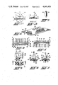
- FIGS. 1A and 1B are views of a prior art surface mounted connector on a printed circuit board, respectively depicting a header so mounted and an enlargement of one of the header bent contacts showing the forces applied during removal of a portable connector;
- FIG. 2 is an isometric view of a printed circuit board with electrical components in the form of headers mounted thereon in accordance with the present invention with other surface mount components--the stand offs on the header bodies are not shown in this figure for facility and clarity;
- FIGS. 3 and 4 are, respectively, top and bottom isometric views of a header connector component in accordance with the present invention.
- FIG. 5 is an enlarged fragmentary isometric view of a pin contact of the header connector component in accordance with the present invention.
- FIG. 6 is an enlarged fragmentary section view of a plated through hole of the printed circuit board of FIG. 2;
- FIG. 7 is a top view of the plated through hole of FIG. 6 looking generally in the direction of the arrows 7--7 of FIG. 6;
- FIG. 8 is an enlarged fragmentary section view of the header positioned in the printed circuit board prior to soldering
- FIG. 9 is an enlarged fragmentary section view of the header positioned in the printed circuit board after soldering
- FIG. 10 is a schematic view of an automated machine for placing surface mount components in a printed circuit board.
- FIG. 11 is a schematic view of a vapor phase solder environment in which soldering of surface mount and connector components according to the invention may be carried out.
- FIGS. 1A and 1B a printed circuit board 1 on which surface mount components are to be mounted and on which an electrical connector 2 in the form of a header 3 with bent contacts 4, 5 is illustrated.
- the printed circuit board 1 has plural printed circuit traces 6, 7 printed or otherwise formed on the surface 8 thereof, each preferably having one or more mounting pads sometimes called solder pads 10, 11 electrically connected therewith and on which a surface mount component may be mounted and electrically connected.
- the header 3 is formed of a body 12 of electrically non-conductive material that preferably is molded about a portion of each of the contacts 4, 5 to hold the same in the parallel alignment shown at available contacting portions 13 while also maintaining the bent contact ends 4, 5 in position to be attached to respective pads 10, 11.
- the header and other surface mount components may be vapor phase or otherwise soldered in place.
- the relatively large amount of space required by the contacts 4, 5 on the surface 8 of the printed circuit board 1 is evident from FIGS. 1A and 1B; to avoid breaking the contacts 4, 5 it is necessary that the curvature thereof be somewhat gradual and, therefore, more space consuming.
- the force applied to the contact 4 of the header 3 is represented generally by the vector 14 which can be resolved to a substantial vertical force concentration that tends to tear at the solder 15 in a direction in which there is a weakness in the solder, e.g. the solder is thin and there is minimal grasping force of the contact 4 in such direction, and in the pad 10 and a horizontal force component. Indeed, such tearing action can too easily damage the integrity of the connection between the contact 4 and the pad 10 and possibly also can damage the integrity of the pad vis-a-vis connection to the surface 8.
- FIG. 2 a printed circuit board 20 having a single header 21 and a pair of parallel headers 22, 23 mounted thereon is illustrated. Also mounted on the printed circuit board surface 24 are several surface mount electrical components 25, such as leaded or unleaded chip carriers, etc.
- the fundamental components of the invention such as an electrical component in the form of the header 21, of the invention include an electrically non-conductive body 30, one and preferably a plurality of electrical leads 31 supported by or protruding from such body, and a reservoir 32 formed in the body for retaining or helping to retain a quantity of solder or solder type material 33, all of which are illustrated in FIGS. 3 and 4.
- the invention also relates to respective plated through holes 34 (FIG. 6) through the printed circuit board 20 and through which respective electrical leads 31 pass to complete a connection of a header to the printed circuit board.
- the body 30 is of electrically non-conductive material capable of withstanding the temperatures and other environmental conditions experienced during the process by which the surface mount components are secured to the printed circuit board, e.g. during a vapor phase soldering process, etc. Such temperatures and environmental conditions may be more severe than those experienced in the past using conventional wave soldering techniques wherein the heat of the solder wave usually is kept remotely from the components, i.e. on the opposite side of the printed circuit board from the component.
- the body 30 is of rectangular cross section having top and bottom surfaces 35, 36 through which the leads, in the form of pin contacts 31, protrude or extend, and side surfaces 37, 38.
- the reservoirs 32 are recesses formed between respective pairs of stand off protrusions 39 that extend from the surface 36, such reservoirs, then, generally circumscribing the areas where the respective pin contacts protrude out from the surface 36.
- the reservoirs may be formed of raised ring-like or other shape walls and/or recesses formed on the bottom surface 36 of the body 30.
- the side surfaces 37, 38 preferably are of a shape that permits one surface to slide along the other. More specifically, the surfaces 37, 38 are generally smooth except for a groove 40 formed in the surface 37 and a flange, tab or tongue 40 formed in the surface 38.
- the tab of one header may slide in the groove of an adjacent one to facilitate the mentioned automated handling, as is described further below.
- Such tab and groove arrangement also may help to secure the two headers 22, 23 (FIG. 2) with respect to each other to reinforce their retention on the printed circuit board 20.
- the pin contacts 31 preferably are elongate, most preferably they are straight, although special curvature at appropriate locations may be included, if desired, for example to help retain the same in the body 30 or for other mechanical or electrical connection purpose.
- the pin contacts 31 extend beyond the top of the header body 30 a distance adequate to facilitate secure attachment to respective female contacts or the like thereto, as is shown at 31T, and the pin contacts 31 extend beyond the bottom of the header an adequate distance to pass through the plated through holes 34, as is shown at 31B.
- the cross section of the pin contacts or leads 31 may be is rectangular, for example square; alternatively, they may be generally circular. A rectangular cross section, though, ordinarily provides greater strength than round cross section.
- pin contacts do not have to bend to the extent that the leads 4, 5 (FIG. 1A) are bent, such pin contacts 31 do not have to be as long as those leads 4, 5, thus further reducing cost and importantly reducing space requirements in directions parallel to the plane of the printed circuit board 20 and through the printed circuit board.
- FIGS. 6 and 7 the plated through holes 34 are shown. Such holes are through the printed circuit board 20, are plated, and preferably are coupled electrically to printed circuit traces 51 on the printed circuit board in usual manner.
- the relation of the cross sectional size or dimension of the plated through holes to that of the pin contacts is such that will minimize, indeed preferably will avoid any, insertion forces of the pin contacts 31 into the board 20 and facilitate pin to hole alignment during manufacturing, which may be particularly advantageous when using automated, e.g. robotic, manuracturing techniques.
- the noted cross sectional relation is such that there is at least some space between part of the faces 52 of the pin contacts 31 and the sides 53 of the holes. Such space 54 is provided to permit the flow of solder therein, e.g. when the solder type material 33 is reflowed during the surface mount process.
- Placement of the header 21 in the printed circuit board 20 is shown in enlargement in FIGS. 8 and 9, the former before soldering and the latter afterwards.
- the bottom end of the pin contact 31 is inserted into the plated through hole 34 to such extent that preferably the solder supply 33 is in engagement with the printed circuit board top surface or with the plated through hole and/or adjacent trace printed thereon.
- the recessed area in the header body 30 between stand offs provides the reservoir 32 and allows a relatively large amount of solder, in any event the amount needed to complete a secure soldering process while permitting the body to be positioned rather close to the top surface of the printed circuit board to minimize height above board requirements and to maximize strength parameters.
- the stand offs provide space above board to permit cleaning of the board surface to remove residual flux from the solder surfaces.
- the open areas between stand offs also may improve heat penetration to the solder supply to melt the same, and to assure melted solder flows to proper locations, i.e. down the hole and to form the desired meniscus 55 and meniscus 56, as is seen in FIG. 9, without causing any short circuiting to other pin contacts, printed circuit traces, etc.
- the stand offs 39 themselves also may help prevent short circuiting between adjacent pin contacts 31 and of the circuits to which they may be connected.
- the solder supply 33 may be an electronic solder paste, such as that sold by Alpha Metals Inc., Jersey City, N.J., U.S.A. that can be placed in the reservoirs 32 between respective stand offs 39, for example by using a syringe type device.
- Such solder paste may be cured in usual fashion, e.g. by heat, to prevent the same from being sticky and, thus, to facilitate shipping and handling and to extend shelf life.
- the header pin contacts 31 are inserted into respective plated through holes.
- the solder supply 33 in each reservoir 32 is heated, melts and by capillary action, gravity, etc. flows into the space 54 and then solidifies.
- the reflowed solder 57 can be seen filling the space 54 and also forming the meniscus 55 at the top of the printed circuit board and the further meniscus 56 at the bottom of the hole in the printed circuit board.
- Each meniscus helps to assure effective electrical connection, provides some degree of compliance factor as parts mechanically are bent, stressed, etc., and tends to maintain cleanliness of the areas where the majority of the pin contacts, plating in the plated through holes, and solder engaged with both of the latter are mechanically and electrically coupled.
- the quantity of the solder supply 33 in each reservoir 32 is adequate when reflowed to fill the space 54 and to form te menisci 55, 56 extending along the pin contact 31 beyond the plane of the board 20 at the top and bottom surfaces thereof for the aforementioned reasons, i.e. to achieve the above advantages of the invention. Too little solder may result in the space 54 not being filled and/or one or both of the menisci being too short or even recessed within the hole 34.
- solder may be achieved using vapor phase soldering or other technique employed for surface mount electrical and mechanical attachment processes vis-a-vis surface mount electrical components and printed circuit boards or the like intended to carry the same.
- solder supply 33 and reservoir 32 therefor is that since the solder material is provided in a reservoir on the connector or other electrical component, i.e. the header 21, rather than as a coating or layer on the pin contact or on the plating of the plated through hole, the possibility of scraping away the solder during insertion of the pin contact into the hole is avoided. Moreover, such reservoir of solder preferably permits adequate amount thereof to be carried for filling the space 54 for strength and integrity of the mechanical and electrical connections to be made.
- An automated apparatus for assembling printed circuit boards with surface mount components is shown schematically at 70 in FIG. 10.
- Such machine includes a support 71 for a printed circuit board, with conventional alignment mechanism for placing, loading, and/or holding the board 20 in proper alignment.
- An exemplary support for the board 20 is shown at 72.
- the machine 70 also includes a supply 74 of surface mount components and/or other electrical and electronic components, a robotic mechanism 75, such as a robotic arm with appropriate movement and retention capabilities, and a controller 76.
- the controller 76 may be a computer control device of conventional design programmed in conventional manner to operate the supply 74 to provide surface mount components for pick up and delivery to the printed circuit board 20 by the robotic arm 75 and, of course, also to operate such arm.
- Such apparatus may be generally of the type that is employed in automated surface mount manufacturing processes, and operation of such apparatus may be generally as is conventional for such apparatus as used in surface mount manufacturing processes.
- the supply 74 includes, for example, a supply of conventional surface mount components, such as PLCC (plastic leaded or unleaded chip carrier) and/or other devices in a holder, all generally designated 77, and a further holder 78 for containing a supply of a plurality of headers 21 in stacked relation.
- a pusher 79 for pushing a header 21 out from between guides 80 along a table 81 into position for pick up by the arm 75 both under operative control of the controller 76. Since the side surfaces of the header bodies 30 are smooth or in any event designed to slide over each other and especially in view of the tab 40 and groove 41 configuration thereof, such sliding in an accurately determined manner can be accomplished to facilitate use with and positioning by the automated apparatus 70.
- the header upon being picked up by the robotic arm 75, the header may be conveniently rotated by the arm and is placed properly in the plated through holes provided therefor in the printed circuit board 20.
- the assembled printed circuit board 20 with several surface mount electrical components, such as PLCC and header/connector devices, positioned thereon is shown placed in a heated environment 82 in which vapor phase soldering of such components and printed circuit board can be accomplished in conventional manner.
- solder already pre-placed on the printed circuit board and/or on the components (ordinarily except for the header or other components that are to be secured to the printed circuit board in the manner described in detail above with respect to the header 21) will be reflowed to complete mechanical and electrical connections.
- the solder supply 33 will reflow in the manner described above to complete the connections shown in detail in FIG. 9.
- the invention may be used to secure mechanically and electrically electrical components, such as connectors, more particularly headers, and the like to printed circuit boards or other surfaces or supports for such components in a way that is compatible with surface mount processes and while maintaining the space utilization efficiency offered by surface mount technology.
Abstract
Description
Claims (31)
Priority Applications (8)
| Application Number | Priority Date | Filing Date | Title |
|---|---|---|---|
| US06/747,343 US4641426A (en) | 1985-06-21 | 1985-06-21 | Surface mount compatible connector system with mechanical integrity |
| US06/782,351 US4663815A (en) | 1985-06-21 | 1985-10-01 | A method and apparatus for surface mount compatible connector system with mechanical integrity |
| AU61235/86A AU6123586A (en) | 1985-06-21 | 1986-06-16 | Surface mount compatible connector system with mechanical integrity |
| PCT/US1986/001310 WO1986007663A1 (en) | 1985-06-21 | 1986-06-16 | Surface mount compatible connector system with mechanical integrity |
| EP19860904530 EP0231258A4 (en) | 1985-06-21 | 1986-06-16 | Surface mount compatible connector system with mechanical integrity. |
| JP61503554A JPS63500277A (en) | 1985-06-21 | 1986-06-16 | Connector system compatible with surface mounts with mechanical integrity |
| CA000511948A CA1265218A (en) | 1985-06-21 | 1986-06-19 | Surface mount compatible connector system with mechanical integrity |
| US07/217,130 US4884335A (en) | 1985-06-21 | 1988-06-29 | Surface mount compatible connector system with solder strip and mounting connector to PCB |
Applications Claiming Priority (1)
| Application Number | Priority Date | Filing Date | Title |
|---|---|---|---|
| US06/747,343 US4641426A (en) | 1985-06-21 | 1985-06-21 | Surface mount compatible connector system with mechanical integrity |
Related Child Applications (2)
| Application Number | Title | Priority Date | Filing Date |
|---|---|---|---|
| US06/782,351 Continuation-In-Part US4663815A (en) | 1985-06-21 | 1985-10-01 | A method and apparatus for surface mount compatible connector system with mechanical integrity |
| US1219187A Continuation-In-Part | 1985-06-21 | 1987-02-09 |
Publications (1)
| Publication Number | Publication Date |
|---|---|
| US4641426A true US4641426A (en) | 1987-02-10 |
Family
ID=25004675
Family Applications (1)
| Application Number | Title | Priority Date | Filing Date |
|---|---|---|---|
| US06/747,343 Expired - Fee Related US4641426A (en) | 1985-06-21 | 1985-06-21 | Surface mount compatible connector system with mechanical integrity |
Country Status (2)
| Country | Link |
|---|---|
| US (1) | US4641426A (en) |
| JP (1) | JPS63500277A (en) |
Cited By (66)
| Publication number | Priority date | Publication date | Assignee | Title |
|---|---|---|---|---|
| US4842184A (en) * | 1988-06-23 | 1989-06-27 | Ltv Aerospace & Defense Company | Method and apparatus for applying solder preforms |
| US4872846A (en) * | 1988-07-21 | 1989-10-10 | Clark Thomas C | Solder containing electrical connector and method for making same |
| US4955523A (en) * | 1986-12-17 | 1990-09-11 | Raychem Corporation | Interconnection of electronic components |
| DE8910105U1 (en) * | 1989-08-23 | 1990-12-20 | Grote & Hartmann Gmbh & Co Kg, 5600 Wuppertal, De | |
| US4984359A (en) * | 1988-07-21 | 1991-01-15 | Amp Incorporated | Method of making a solder containing electrical connector |
| US5022862A (en) * | 1986-11-12 | 1991-06-11 | Societe C E T R A | Modular connector |
| US5046957A (en) * | 1990-06-25 | 1991-09-10 | Amp Incorporated | Solder plate assembly and method |
| US5059130A (en) * | 1988-06-23 | 1991-10-22 | Ltv Aerospace And Defense Company | Minimal space printed cicuit board and electrical connector system |
| US5083696A (en) * | 1989-06-07 | 1992-01-28 | E. I. Du Pont De Nemours And Company | Pin-holding device for use in connecting a pin |
| US5092035A (en) * | 1990-09-10 | 1992-03-03 | Codex Corporation | Method of making printed circuit board assembly |
| US5189507A (en) * | 1986-12-17 | 1993-02-23 | Raychem Corporation | Interconnection of electronic components |
| US5225897A (en) * | 1991-10-02 | 1993-07-06 | Unitrode Corporation | Molded package for semiconductor devices with leadframe locking structure |
| US5268819A (en) * | 1991-03-19 | 1993-12-07 | Nokia Mobile Phones Ltd. | Circuit board assembly |
| US5325305A (en) * | 1992-07-24 | 1994-06-28 | The Boeing Company | Automated setup verification system |
| US5451174A (en) * | 1993-06-29 | 1995-09-19 | Autosplice Systems, Inc. | Surface mounted pins for printed circuit boards |
| WO1997016870A1 (en) * | 1995-11-03 | 1997-05-09 | North American Specialties Corporation | Solder-holding clips for applying solder to connectors |
| US5816868A (en) * | 1996-02-12 | 1998-10-06 | Zierick Manufacturing Corp. | Capillary action promoting surface mount connectors |
| US5820014A (en) | 1993-11-16 | 1998-10-13 | Form Factor, Inc. | Solder preforms |
| US5994152A (en) | 1996-02-21 | 1999-11-30 | Formfactor, Inc. | Fabricating interconnects and tips using sacrificial substrates |
| US6024584A (en) * | 1996-10-10 | 2000-02-15 | Berg Technology, Inc. | High density connector |
| US6042389A (en) * | 1996-10-10 | 2000-03-28 | Berg Technology, Inc. | Low profile connector |
| US6093035A (en) * | 1996-06-28 | 2000-07-25 | Berg Technology, Inc. | Contact for use in an electrical connector |
| US6137061A (en) * | 1997-08-01 | 2000-10-24 | Lucent Technologies Inc. | Reduction of parasitic through hole via capacitance in multilayer printed circuit boards |
| US6139336A (en) * | 1996-11-14 | 2000-10-31 | Berg Technology, Inc. | High density connector having a ball type of contact surface |
| US6146203A (en) * | 1995-06-12 | 2000-11-14 | Berg Technology, Inc. | Low cross talk and impedance controlled electrical connector |
| US6241535B1 (en) | 1996-10-10 | 2001-06-05 | Berg Technology, Inc. | Low profile connector |
| US6274823B1 (en) | 1993-11-16 | 2001-08-14 | Formfactor, Inc. | Interconnection substrates with resilient contact structures on both sides |
| US6325644B1 (en) | 1996-10-10 | 2001-12-04 | Berg Technology, Inc. | High density connector and method of manufacture |
| US6595788B2 (en) * | 1999-10-14 | 2003-07-22 | Berg Technology, Inc. | Electrical connector with continuous strip contacts |
| US6665930B2 (en) * | 1998-03-04 | 2003-12-23 | Koninklijke Philips Electronics N.V. | Printed circuit board with SMD components |
| US6939173B1 (en) | 1995-06-12 | 2005-09-06 | Fci Americas Technology, Inc. | Low cross talk and impedance controlled electrical connector with solder masses |
| US20050221675A1 (en) * | 2003-07-16 | 2005-10-06 | Rathburn James J | Fine pitch electrical interconnect assembly |
| US20060035483A1 (en) * | 2003-07-16 | 2006-02-16 | Gryphics, Inc. | Fine pitch electrical interconnect assembly |
| US20060237856A1 (en) * | 1993-11-16 | 2006-10-26 | Formfactor, Inc. | Microelectronic Contact Structure And Method Of Making Same |
| FR2895157A1 (en) * | 2005-12-21 | 2007-06-22 | Dav Sa | Male double side printed circuit board connector for automobile field, has connection pins with ends, connected on jumper lugs on one side of board, extending via curved portions partially surrounding part of support matrix |
| US20070218257A1 (en) * | 2004-03-31 | 2007-09-20 | Tsugio Ambo | Circuit board, its manufacturing method, and joint box using circuit board |
| US20080182436A1 (en) * | 2003-07-16 | 2008-07-31 | Gryphics, Inc. | Fine pitch electrical interconnect assembly |
| DE10084996B4 (en) * | 1999-09-20 | 2008-09-18 | Nas Interplex Industries, Inc. | Solder-carrying body for use in soldering operations |
| US20100093229A1 (en) * | 1996-02-21 | 2010-04-15 | Formfactor, Inc. | Microelectronic contact structure and method of making same |
| US20110167628A1 (en) * | 2002-12-10 | 2011-07-14 | Neonode, Inc. | Component bonding using a capillary effect |
| US8044502B2 (en) | 2006-03-20 | 2011-10-25 | Gryphics, Inc. | Composite contact for fine pitch electrical interconnect assembly |
| CN102456968A (en) * | 2010-11-01 | 2012-05-16 | 富士康(昆山)电脑接插件有限公司 | Electric connector combination and manufacturing method for same |
| US20120202371A1 (en) * | 2009-10-06 | 2012-08-09 | Phonak Ag | Integral connector for programming a hearing device |
| US8696367B2 (en) | 2011-01-20 | 2014-04-15 | Genesis Technology Usa, Inc. | Two-piece connector assembly for connecting an electronic device to a circuit board |
| USD718253S1 (en) | 2012-04-13 | 2014-11-25 | Fci Americas Technology Llc | Electrical cable connector |
| US8905651B2 (en) | 2012-01-31 | 2014-12-09 | Fci | Dismountable optical coupling device |
| USD720698S1 (en) | 2013-03-15 | 2015-01-06 | Fci Americas Technology Llc | Electrical cable connector |
| US8944831B2 (en) | 2012-04-13 | 2015-02-03 | Fci Americas Technology Llc | Electrical connector having ribbed ground plate with engagement members |
| USD727268S1 (en) | 2012-04-13 | 2015-04-21 | Fci Americas Technology Llc | Vertical electrical connector |
| USD727852S1 (en) | 2012-04-13 | 2015-04-28 | Fci Americas Technology Llc | Ground shield for a right angle electrical connector |
| US9048583B2 (en) | 2009-03-19 | 2015-06-02 | Fci Americas Technology Llc | Electrical connector having ribbed ground plate |
| US9063614B2 (en) | 2009-02-15 | 2015-06-23 | Neonode Inc. | Optical touch screens |
| USD733662S1 (en) | 2013-01-25 | 2015-07-07 | Fci Americas Technology Llc | Connector housing for electrical connector |
| US9207800B1 (en) | 2014-09-23 | 2015-12-08 | Neonode Inc. | Integrated light guide and touch screen frame and multi-touch determination method |
| USD746236S1 (en) | 2012-07-11 | 2015-12-29 | Fci Americas Technology Llc | Electrical connector housing |
| US9257778B2 (en) | 2012-04-13 | 2016-02-09 | Fci Americas Technology | High speed electrical connector |
| US9362638B2 (en) * | 2014-09-03 | 2016-06-07 | Amphenol Corporation | Overmolded contact wafer and connector |
| US9531095B1 (en) * | 2015-12-21 | 2016-12-27 | Viewmove Technologies, Inc. | Communication structure with connecting assembly |
| US9543703B2 (en) | 2012-07-11 | 2017-01-10 | Fci Americas Technology Llc | Electrical connector with reduced stack height |
| US10282034B2 (en) | 2012-10-14 | 2019-05-07 | Neonode Inc. | Touch sensitive curved and flexible displays |
| US20190372253A1 (en) * | 2018-05-30 | 2019-12-05 | Molex, Llc | Socket |
| US11379048B2 (en) | 2012-10-14 | 2022-07-05 | Neonode Inc. | Contactless control panel |
| US20230056822A1 (en) * | 2021-08-18 | 2023-02-23 | Borgwarner Inc. | Circuit board interconnection device and circuit board assembly |
| US11669210B2 (en) | 2020-09-30 | 2023-06-06 | Neonode Inc. | Optical touch sensor |
| US11733808B2 (en) | 2012-10-14 | 2023-08-22 | Neonode, Inc. | Object detector based on reflected light |
| US11842014B2 (en) | 2019-12-31 | 2023-12-12 | Neonode Inc. | Contactless touch input system |
Families Citing this family (1)
| Publication number | Priority date | Publication date | Assignee | Title |
|---|---|---|---|---|
| JP2795088B2 (en) * | 1992-09-09 | 1998-09-10 | 松下電器産業株式会社 | How to mount components with leads |
Citations (4)
| Publication number | Priority date | Publication date | Assignee | Title |
|---|---|---|---|---|
| US3834015A (en) * | 1973-01-29 | 1974-09-10 | Philco Ford Corp | Method of forming electrical connections |
| US3864014A (en) * | 1972-05-01 | 1975-02-04 | Amp Inc | Coined post for solder stripe |
| US3905665A (en) * | 1971-07-27 | 1975-09-16 | Amp Inc | Electrical contact structure and assembly method |
| US3932934A (en) * | 1974-09-16 | 1976-01-20 | Amp Incorporated | Method of connecting terminal posts of a connector to a circuit board |
-
1985
- 1985-06-21 US US06/747,343 patent/US4641426A/en not_active Expired - Fee Related
-
1986
- 1986-06-16 JP JP61503554A patent/JPS63500277A/en active Pending
Patent Citations (4)
| Publication number | Priority date | Publication date | Assignee | Title |
|---|---|---|---|---|
| US3905665A (en) * | 1971-07-27 | 1975-09-16 | Amp Inc | Electrical contact structure and assembly method |
| US3864014A (en) * | 1972-05-01 | 1975-02-04 | Amp Inc | Coined post for solder stripe |
| US3834015A (en) * | 1973-01-29 | 1974-09-10 | Philco Ford Corp | Method of forming electrical connections |
| US3932934A (en) * | 1974-09-16 | 1976-01-20 | Amp Incorporated | Method of connecting terminal posts of a connector to a circuit board |
Cited By (116)
| Publication number | Priority date | Publication date | Assignee | Title |
|---|---|---|---|---|
| US5022862A (en) * | 1986-11-12 | 1991-06-11 | Societe C E T R A | Modular connector |
| US5189507A (en) * | 1986-12-17 | 1993-02-23 | Raychem Corporation | Interconnection of electronic components |
| US4955523A (en) * | 1986-12-17 | 1990-09-11 | Raychem Corporation | Interconnection of electronic components |
| US5059130A (en) * | 1988-06-23 | 1991-10-22 | Ltv Aerospace And Defense Company | Minimal space printed cicuit board and electrical connector system |
| US4842184A (en) * | 1988-06-23 | 1989-06-27 | Ltv Aerospace & Defense Company | Method and apparatus for applying solder preforms |
| US4872846A (en) * | 1988-07-21 | 1989-10-10 | Clark Thomas C | Solder containing electrical connector and method for making same |
| US4984359A (en) * | 1988-07-21 | 1991-01-15 | Amp Incorporated | Method of making a solder containing electrical connector |
| US5083696A (en) * | 1989-06-07 | 1992-01-28 | E. I. Du Pont De Nemours And Company | Pin-holding device for use in connecting a pin |
| DE8910105U1 (en) * | 1989-08-23 | 1990-12-20 | Grote & Hartmann Gmbh & Co Kg, 5600 Wuppertal, De | |
| US5046957A (en) * | 1990-06-25 | 1991-09-10 | Amp Incorporated | Solder plate assembly and method |
| WO1992004812A1 (en) * | 1990-09-10 | 1992-03-19 | Codex Corporation | Printed circuit board manufacturing method accommodates wave soldering and press fitting of components |
| US5092035A (en) * | 1990-09-10 | 1992-03-03 | Codex Corporation | Method of making printed circuit board assembly |
| US5268819A (en) * | 1991-03-19 | 1993-12-07 | Nokia Mobile Phones Ltd. | Circuit board assembly |
| US5225897A (en) * | 1991-10-02 | 1993-07-06 | Unitrode Corporation | Molded package for semiconductor devices with leadframe locking structure |
| US5325305A (en) * | 1992-07-24 | 1994-06-28 | The Boeing Company | Automated setup verification system |
| US5451174A (en) * | 1993-06-29 | 1995-09-19 | Autosplice Systems, Inc. | Surface mounted pins for printed circuit boards |
| US20060237856A1 (en) * | 1993-11-16 | 2006-10-26 | Formfactor, Inc. | Microelectronic Contact Structure And Method Of Making Same |
| US6274823B1 (en) | 1993-11-16 | 2001-08-14 | Formfactor, Inc. | Interconnection substrates with resilient contact structures on both sides |
| US5820014A (en) | 1993-11-16 | 1998-10-13 | Form Factor, Inc. | Solder preforms |
| US6146203A (en) * | 1995-06-12 | 2000-11-14 | Berg Technology, Inc. | Low cross talk and impedance controlled electrical connector |
| US6939173B1 (en) | 1995-06-12 | 2005-09-06 | Fci Americas Technology, Inc. | Low cross talk and impedance controlled electrical connector with solder masses |
| WO1997016870A1 (en) * | 1995-11-03 | 1997-05-09 | North American Specialties Corporation | Solder-holding clips for applying solder to connectors |
| US6099365A (en) * | 1995-11-03 | 2000-08-08 | North American Specialties Corporation | Solder-holding clips for applying solder to connectors or the like |
| US5875546A (en) * | 1995-11-03 | 1999-03-02 | North American Specialties Corporation | Method of forming solder-holding clips for applying solder to connectors |
| US6494754B2 (en) | 1995-11-03 | 2002-12-17 | North American Specialties | Solder-holding clips for applying solder to connectors or the like |
| US6402574B2 (en) * | 1995-11-03 | 2002-06-11 | North American Specialties Corporation | Solder-holding clips for applying solder to connectors or the like |
| DE19704930B4 (en) * | 1996-02-12 | 2008-05-29 | Zierick Mfg. Corp. | Surface mount connectors that promote capillary action |
| US5816868A (en) * | 1996-02-12 | 1998-10-06 | Zierick Manufacturing Corp. | Capillary action promoting surface mount connectors |
| US5994152A (en) | 1996-02-21 | 1999-11-30 | Formfactor, Inc. | Fabricating interconnects and tips using sacrificial substrates |
| US20100093229A1 (en) * | 1996-02-21 | 2010-04-15 | Formfactor, Inc. | Microelectronic contact structure and method of making same |
| US8033838B2 (en) | 1996-02-21 | 2011-10-11 | Formfactor, Inc. | Microelectronic contact structure |
| US6093035A (en) * | 1996-06-28 | 2000-07-25 | Berg Technology, Inc. | Contact for use in an electrical connector |
| US6042389A (en) * | 1996-10-10 | 2000-03-28 | Berg Technology, Inc. | Low profile connector |
| US6164983A (en) * | 1996-10-10 | 2000-12-26 | Berg Technology, Inc. | High density connector |
| US6358068B1 (en) | 1996-10-10 | 2002-03-19 | Fci Americas Technology, Inc. | Stress resistant connector and method for reducing stress in housing thereof |
| US6024584A (en) * | 1996-10-10 | 2000-02-15 | Berg Technology, Inc. | High density connector |
| US6241535B1 (en) | 1996-10-10 | 2001-06-05 | Berg Technology, Inc. | Low profile connector |
| US8167630B2 (en) | 1996-10-10 | 2012-05-01 | Fci Americas Technology Llc | High density connector and method of manufacture |
| US20080032524A1 (en) * | 1996-10-10 | 2008-02-07 | Lemke Timothy A | High Density Connector and Method of Manufacture |
| US6325644B1 (en) | 1996-10-10 | 2001-12-04 | Berg Technology, Inc. | High density connector and method of manufacture |
| US7186123B2 (en) | 1996-10-10 | 2007-03-06 | Fci Americas Technology, Inc. | High density connector and method of manufacture |
| US20050079763A1 (en) * | 1996-10-10 | 2005-04-14 | Lemke Timothy A. | High density connector and method of manufacture |
| US6079991A (en) * | 1996-10-10 | 2000-06-27 | Berg Technology, Inc. | Method for placing contact on electrical connector |
| US6139336A (en) * | 1996-11-14 | 2000-10-31 | Berg Technology, Inc. | High density connector having a ball type of contact surface |
| US6247635B1 (en) | 1996-11-14 | 2001-06-19 | Berg Technology, Inc. | High density connector having a ball type of contact surface |
| US6137061A (en) * | 1997-08-01 | 2000-10-24 | Lucent Technologies Inc. | Reduction of parasitic through hole via capacitance in multilayer printed circuit boards |
| US6665930B2 (en) * | 1998-03-04 | 2003-12-23 | Koninklijke Philips Electronics N.V. | Printed circuit board with SMD components |
| DE10084996B8 (en) * | 1999-09-20 | 2009-01-29 | Nas Interplex Industries Inc. | Solder-carrying body for use in soldering operations |
| DE10084996B4 (en) * | 1999-09-20 | 2008-09-18 | Nas Interplex Industries, Inc. | Solder-carrying body for use in soldering operations |
| US6971889B2 (en) | 1999-10-14 | 2005-12-06 | Berg Technology, Inc | Electrical connector with continuous strip contacts |
| US6712626B2 (en) | 1999-10-14 | 2004-03-30 | Berg Technology, Inc. | Electrical connector with continuous strip contacts |
| US6595788B2 (en) * | 1999-10-14 | 2003-07-22 | Berg Technology, Inc. | Electrical connector with continuous strip contacts |
| US20040171310A1 (en) * | 1999-10-14 | 2004-09-02 | Berg Technology, Inc. | Electrical connector with continuous strip contacts |
| US8403203B2 (en) * | 2002-12-10 | 2013-03-26 | Neonoda Inc. | Component bonding using a capillary effect |
| US20110167628A1 (en) * | 2002-12-10 | 2011-07-14 | Neonode, Inc. | Component bonding using a capillary effect |
| US7422439B2 (en) | 2003-07-16 | 2008-09-09 | Gryphics, Inc. | Fine pitch electrical interconnect assembly |
| US7297003B2 (en) | 2003-07-16 | 2007-11-20 | Gryphics, Inc. | Fine pitch electrical interconnect assembly |
| US20080182436A1 (en) * | 2003-07-16 | 2008-07-31 | Gryphics, Inc. | Fine pitch electrical interconnect assembly |
| US20050221675A1 (en) * | 2003-07-16 | 2005-10-06 | Rathburn James J | Fine pitch electrical interconnect assembly |
| US7537461B2 (en) | 2003-07-16 | 2009-05-26 | Gryphics, Inc. | Fine pitch electrical interconnect assembly |
| US20080057753A1 (en) * | 2003-07-16 | 2008-03-06 | Gryphics, Inc | Fine pitch electrical interconnect assembly |
| US20060035483A1 (en) * | 2003-07-16 | 2006-02-16 | Gryphics, Inc. | Fine pitch electrical interconnect assembly |
| US7326064B2 (en) | 2003-07-16 | 2008-02-05 | Gryphics, Inc. | Fine pitch electrical interconnect assembly |
| US20110116248A1 (en) * | 2004-03-31 | 2011-05-19 | Mitsubishi Cable Industries, Ltd. | Circuit board, its manufacturing method, and joint box using circuit board |
| US7943859B2 (en) * | 2004-03-31 | 2011-05-17 | Mitsubishi Cable Industries, Ltd. | Circuit board, its manufacturing method, and joint box using circuit board |
| US8362366B2 (en) * | 2004-03-31 | 2013-01-29 | Mitsubishi Cable Industries, Ltd. | Circuit board, its manufacturing method, and joint box using circuit board |
| US20070218257A1 (en) * | 2004-03-31 | 2007-09-20 | Tsugio Ambo | Circuit board, its manufacturing method, and joint box using circuit board |
| FR2895157A1 (en) * | 2005-12-21 | 2007-06-22 | Dav Sa | Male double side printed circuit board connector for automobile field, has connection pins with ends, connected on jumper lugs on one side of board, extending via curved portions partially surrounding part of support matrix |
| US8044502B2 (en) | 2006-03-20 | 2011-10-25 | Gryphics, Inc. | Composite contact for fine pitch electrical interconnect assembly |
| US8232632B2 (en) | 2006-03-20 | 2012-07-31 | R&D Sockets, Inc. | Composite contact for fine pitch electrical interconnect assembly |
| US9678601B2 (en) | 2009-02-15 | 2017-06-13 | Neonode Inc. | Optical touch screens |
| US9063614B2 (en) | 2009-02-15 | 2015-06-23 | Neonode Inc. | Optical touch screens |
| US10720721B2 (en) | 2009-03-19 | 2020-07-21 | Fci Usa Llc | Electrical connector having ribbed ground plate |
| US10096921B2 (en) | 2009-03-19 | 2018-10-09 | Fci Usa Llc | Electrical connector having ribbed ground plate |
| US9461410B2 (en) | 2009-03-19 | 2016-10-04 | Fci Americas Technology Llc | Electrical connector having ribbed ground plate |
| US9048583B2 (en) | 2009-03-19 | 2015-06-02 | Fci Americas Technology Llc | Electrical connector having ribbed ground plate |
| US8651895B2 (en) * | 2009-10-06 | 2014-02-18 | Phonak Ag | Integral connector for programming a hearing device |
| US20120202371A1 (en) * | 2009-10-06 | 2012-08-09 | Phonak Ag | Integral connector for programming a hearing device |
| CN102456968B (en) * | 2010-11-01 | 2015-07-08 | 富士康(昆山)电脑接插件有限公司 | Electric connector combination and manufacturing method for same |
| CN102456968A (en) * | 2010-11-01 | 2012-05-16 | 富士康(昆山)电脑接插件有限公司 | Electric connector combination and manufacturing method for same |
| US8696367B2 (en) | 2011-01-20 | 2014-04-15 | Genesis Technology Usa, Inc. | Two-piece connector assembly for connecting an electronic device to a circuit board |
| US8905651B2 (en) | 2012-01-31 | 2014-12-09 | Fci | Dismountable optical coupling device |
| US9831605B2 (en) | 2012-04-13 | 2017-11-28 | Fci Americas Technology Llc | High speed electrical connector |
| US8944831B2 (en) | 2012-04-13 | 2015-02-03 | Fci Americas Technology Llc | Electrical connector having ribbed ground plate with engagement members |
| USD816044S1 (en) | 2012-04-13 | 2018-04-24 | Fci Americas Technology Llc | Electrical cable connector |
| USD727268S1 (en) | 2012-04-13 | 2015-04-21 | Fci Americas Technology Llc | Vertical electrical connector |
| USD790471S1 (en) | 2012-04-13 | 2017-06-27 | Fci Americas Technology Llc | Vertical electrical connector |
| USD748063S1 (en) | 2012-04-13 | 2016-01-26 | Fci Americas Technology Llc | Electrical ground shield |
| US9257778B2 (en) | 2012-04-13 | 2016-02-09 | Fci Americas Technology | High speed electrical connector |
| USD750030S1 (en) | 2012-04-13 | 2016-02-23 | Fci Americas Technology Llc | Electrical cable connector |
| USD750025S1 (en) | 2012-04-13 | 2016-02-23 | Fci Americas Technology Llc | Vertical electrical connector |
| USD718253S1 (en) | 2012-04-13 | 2014-11-25 | Fci Americas Technology Llc | Electrical cable connector |
| USD727852S1 (en) | 2012-04-13 | 2015-04-28 | Fci Americas Technology Llc | Ground shield for a right angle electrical connector |
| US9543703B2 (en) | 2012-07-11 | 2017-01-10 | Fci Americas Technology Llc | Electrical connector with reduced stack height |
| USD751507S1 (en) | 2012-07-11 | 2016-03-15 | Fci Americas Technology Llc | Electrical connector |
| US9871323B2 (en) | 2012-07-11 | 2018-01-16 | Fci Americas Technology Llc | Electrical connector with reduced stack height |
| USD746236S1 (en) | 2012-07-11 | 2015-12-29 | Fci Americas Technology Llc | Electrical connector housing |
| US10949027B2 (en) | 2012-10-14 | 2021-03-16 | Neonode Inc. | Interactive virtual display |
| US10282034B2 (en) | 2012-10-14 | 2019-05-07 | Neonode Inc. | Touch sensitive curved and flexible displays |
| US11733808B2 (en) | 2012-10-14 | 2023-08-22 | Neonode, Inc. | Object detector based on reflected light |
| US11714509B2 (en) | 2012-10-14 | 2023-08-01 | Neonode Inc. | Multi-plane reflective sensor |
| US11379048B2 (en) | 2012-10-14 | 2022-07-05 | Neonode Inc. | Contactless control panel |
| USD772168S1 (en) | 2013-01-25 | 2016-11-22 | Fci Americas Technology Llc | Connector housing for electrical connector |
| USD733662S1 (en) | 2013-01-25 | 2015-07-07 | Fci Americas Technology Llc | Connector housing for electrical connector |
| USD766832S1 (en) | 2013-01-25 | 2016-09-20 | Fci Americas Technology Llc | Electrical connector |
| USD745852S1 (en) | 2013-01-25 | 2015-12-22 | Fci Americas Technology Llc | Electrical connector |
| USD720698S1 (en) | 2013-03-15 | 2015-01-06 | Fci Americas Technology Llc | Electrical cable connector |
| US9362638B2 (en) * | 2014-09-03 | 2016-06-07 | Amphenol Corporation | Overmolded contact wafer and connector |
| US9645679B2 (en) | 2014-09-23 | 2017-05-09 | Neonode Inc. | Integrated light guide and touch screen frame |
| US9207800B1 (en) | 2014-09-23 | 2015-12-08 | Neonode Inc. | Integrated light guide and touch screen frame and multi-touch determination method |
| US9531095B1 (en) * | 2015-12-21 | 2016-12-27 | Viewmove Technologies, Inc. | Communication structure with connecting assembly |
| US20190372253A1 (en) * | 2018-05-30 | 2019-12-05 | Molex, Llc | Socket |
| US10840620B2 (en) * | 2018-05-30 | 2020-11-17 | Molex, Llc | Socket |
| US11842014B2 (en) | 2019-12-31 | 2023-12-12 | Neonode Inc. | Contactless touch input system |
| US11669210B2 (en) | 2020-09-30 | 2023-06-06 | Neonode Inc. | Optical touch sensor |
| US20230056822A1 (en) * | 2021-08-18 | 2023-02-23 | Borgwarner Inc. | Circuit board interconnection device and circuit board assembly |
Also Published As
| Publication number | Publication date |
|---|---|
| JPS63500277A (en) | 1988-01-28 |
Similar Documents
| Publication | Publication Date | Title |
|---|---|---|
| US4641426A (en) | Surface mount compatible connector system with mechanical integrity | |
| US4884335A (en) | Surface mount compatible connector system with solder strip and mounting connector to PCB | |
| US4663815A (en) | A method and apparatus for surface mount compatible connector system with mechanical integrity | |
| US5451174A (en) | Surface mounted pins for printed circuit boards | |
| US5984692A (en) | Board stacking connector chip and tape cartridge containing the chip | |
| US6398559B2 (en) | Connecting terminal and a connecting terminal assembly | |
| US5129573A (en) | Method for attaching through-hole devices to a circuit board using solder paste | |
| US5709574A (en) | Surface-mountable socket connector | |
| US4550959A (en) | Surface mountable coefficient of expansion matching connector | |
| EP0480754B1 (en) | Mounting device for mounting an electronic device on a substrate by the surface mounting technology | |
| EP0562725A2 (en) | Adaptor element for modifying electrical connections to an electrical component | |
| US6780028B1 (en) | Solder reserve transfer device and process | |
| EP0206619B1 (en) | Self-soldering, flexible circuit connector | |
| US6475023B2 (en) | Surface mount holding feature | |
| US4661887A (en) | Surface mountable integrated circuit packages having solder bearing leads | |
| JPH0917475A (en) | Surface installation contact, surface installation jumper, roll of surface installation contact, roll of surface installation jumper, surface installation contact strip formation and surface installation jumper strip formation | |
| JP3288654B2 (en) | Method of manufacturing electrical connector | |
| US4846702A (en) | Electrical connector for surface mount chip carrier installed in a socket | |
| EP0125780A1 (en) | Surface mountable expansion matching connector | |
| US7465173B2 (en) | De-soldering tool | |
| CN1549408A (en) | Method for producing electric connector | |
| JPS60113998A (en) | Electronic part assembly | |
| US6966440B1 (en) | Tape-packaged headed pin contact | |
| JP4523245B2 (en) | Connector with lock | |
| CA2202576C (en) | Electronic circuit assembly |
Legal Events
| Date | Code | Title | Description |
|---|---|---|---|
| AS | Assignment |
Owner name: ASSOCIATED ENTERPRISES, INC. 1382 WEST JACKSON STR Free format text: ASSIGNMENT OF ASSIGNORS INTEREST.;ASSIGNORS:HARTMAN, JOHN E.;VENALECK, JOHN T.;REEL/FRAME:004445/0872 Effective date: 19850724 |
|
| AS | Assignment |
Owner name: MINNESOTA MINING AND MANUFACTURING COMPANY (3M) Free format text: ASSIGNMENT OF ASSIGNORS INTEREST.;ASSIGNOR:ASSOCIATED ENTERPRISES, INC.,;REEL/FRAME:004973/0523 Effective date: 19880722 |
|
| FPAY | Fee payment |
Year of fee payment: 4 |
|
| REMI | Maintenance fee reminder mailed | ||
| LAPS | Lapse for failure to pay maintenance fees | ||
| FP | Lapsed due to failure to pay maintenance fee |
Effective date: 19950215 |
|
| STCH | Information on status: patent discontinuation |
Free format text: PATENT EXPIRED DUE TO NONPAYMENT OF MAINTENANCE FEES UNDER 37 CFR 1.362 |