US4635347A - Method of fabricating titanium silicide gate electrodes and interconnections - Google Patents
Method of fabricating titanium silicide gate electrodes and interconnections Download PDFInfo
- Publication number
- US4635347A US4635347A US06/717,370 US71737085A US4635347A US 4635347 A US4635347 A US 4635347A US 71737085 A US71737085 A US 71737085A US 4635347 A US4635347 A US 4635347A
- Authority
- US
- United States
- Prior art keywords
- titanium
- interconnections
- layer
- gate
- substrate
- Prior art date
- Legal status (The legal status is an assumption and is not a legal conclusion. Google has not performed a legal analysis and makes no representation as to the accuracy of the status listed.)
- Expired - Lifetime
Links
Images

Classifications
-
- H—ELECTRICITY
- H01—ELECTRIC ELEMENTS
- H01L—SEMICONDUCTOR DEVICES NOT COVERED BY CLASS H10
- H01L21/00—Processes or apparatus adapted for the manufacture or treatment of semiconductor or solid state devices or of parts thereof
- H01L21/02—Manufacture or treatment of semiconductor devices or of parts thereof
- H01L21/04—Manufacture or treatment of semiconductor devices or of parts thereof the devices having at least one potential-jump barrier or surface barrier, e.g. PN junction, depletion layer or carrier concentration layer
- H01L21/18—Manufacture or treatment of semiconductor devices or of parts thereof the devices having at least one potential-jump barrier or surface barrier, e.g. PN junction, depletion layer or carrier concentration layer the devices having semiconductor bodies comprising elements of Group IV of the Periodic System or AIIIBV compounds with or without impurities, e.g. doping materials
- H01L21/30—Treatment of semiconductor bodies using processes or apparatus not provided for in groups H01L21/20 - H01L21/26
- H01L21/31—Treatment of semiconductor bodies using processes or apparatus not provided for in groups H01L21/20 - H01L21/26 to form insulating layers thereon, e.g. for masking or by using photolithographic techniques; After treatment of these layers; Selection of materials for these layers
- H01L21/3205—Deposition of non-insulating-, e.g. conductive- or resistive-, layers on insulating layers; After-treatment of these layers
- H01L21/32051—Deposition of metallic or metal-silicide layers
-
- H—ELECTRICITY
- H01—ELECTRIC ELEMENTS
- H01L—SEMICONDUCTOR DEVICES NOT COVERED BY CLASS H10
- H01L21/00—Processes or apparatus adapted for the manufacture or treatment of semiconductor or solid state devices or of parts thereof
- H01L21/70—Manufacture or treatment of devices consisting of a plurality of solid state components formed in or on a common substrate or of parts thereof; Manufacture of integrated circuit devices or of parts thereof
- H01L21/71—Manufacture of specific parts of devices defined in group H01L21/70
- H01L21/768—Applying interconnections to be used for carrying current between separate components within a device comprising conductors and dielectrics
- H01L21/76838—Applying interconnections to be used for carrying current between separate components within a device comprising conductors and dielectrics characterised by the formation and the after-treatment of the conductors
- H01L21/76886—Modifying permanently or temporarily the pattern or the conductivity of conductive members, e.g. formation of alloys, reduction of contact resistances
- H01L21/76889—Modifying permanently or temporarily the pattern or the conductivity of conductive members, e.g. formation of alloys, reduction of contact resistances by forming silicides of refractory metals
-
- H—ELECTRICITY
- H10—SEMICONDUCTOR DEVICES; ELECTRIC SOLID-STATE DEVICES NOT OTHERWISE PROVIDED FOR
- H10B—ELECTRONIC MEMORY DEVICES
- H10B41/00—Electrically erasable-and-programmable ROM [EEPROM] devices comprising floating gates
- H10B41/40—Electrically erasable-and-programmable ROM [EEPROM] devices comprising floating gates characterised by the peripheral circuit region
- H10B41/42—Simultaneous manufacture of periphery and memory cells
- H10B41/43—Simultaneous manufacture of periphery and memory cells comprising only one type of peripheral transistor
- H10B41/44—Simultaneous manufacture of periphery and memory cells comprising only one type of peripheral transistor with a control gate layer also being used as part of the peripheral transistor
-
- H—ELECTRICITY
- H10—SEMICONDUCTOR DEVICES; ELECTRIC SOLID-STATE DEVICES NOT OTHERWISE PROVIDED FOR
- H10B—ELECTRONIC MEMORY DEVICES
- H10B69/00—Erasable-and-programmable ROM [EPROM] devices not provided for in groups H10B41/00 - H10B63/00, e.g. ultraviolet erasable-and-programmable ROM [UVEPROM] devices
-
- Y—GENERAL TAGGING OF NEW TECHNOLOGICAL DEVELOPMENTS; GENERAL TAGGING OF CROSS-SECTIONAL TECHNOLOGIES SPANNING OVER SEVERAL SECTIONS OF THE IPC; TECHNICAL SUBJECTS COVERED BY FORMER USPC CROSS-REFERENCE ART COLLECTIONS [XRACs] AND DIGESTS
- Y10—TECHNICAL SUBJECTS COVERED BY FORMER USPC
- Y10S—TECHNICAL SUBJECTS COVERED BY FORMER USPC CROSS-REFERENCE ART COLLECTIONS [XRACs] AND DIGESTS
- Y10S148/00—Metal treatment
- Y10S148/019—Contacts of silicides
-
- Y—GENERAL TAGGING OF NEW TECHNOLOGICAL DEVELOPMENTS; GENERAL TAGGING OF CROSS-SECTIONAL TECHNOLOGIES SPANNING OVER SEVERAL SECTIONS OF THE IPC; TECHNICAL SUBJECTS COVERED BY FORMER USPC CROSS-REFERENCE ART COLLECTIONS [XRACs] AND DIGESTS
- Y10—TECHNICAL SUBJECTS COVERED BY FORMER USPC
- Y10S—TECHNICAL SUBJECTS COVERED BY FORMER USPC CROSS-REFERENCE ART COLLECTIONS [XRACs] AND DIGESTS
- Y10S148/00—Metal treatment
- Y10S148/147—Silicides
Definitions
- the present invention generally relates to integrated circuits and, in particular, to a method for constructing titanium silicide metal-oxide semiconductor (MOS) integrated circuit electrodes and in interconnections.
- MOS metal-oxide semiconductor
- a MOSFET generally consists of two closely spaced, doped regions in a substrate--the "source” and the “drain.” The region between the two is the “channel.” A thin insulation layer is formed directly above the channel. A conductive material "gate” electrode is positioned directly over and completely covering the insulation layer directly above the channel. A voltage applied to the gate affects the electronic properties of the channel region, whereby the FET is turned ON or OFF.
- a first gate lies below a superposing insulator layer upon which the gate electrode is constructed; the first gate is known as a "floating gate.”
- MOS has become somewhat of a misnomer because for many applications these gates are formed of a polysilicon material which is doped to render it conductive. However, although such a gate is adequate to create a field in the channel region so as to control the state of the FET, it is not without its operational problems.
- U.S. Pat. No. 4,443,930 teaches a method of cosputtering a target of metal silicide and a target of doped silicon to form a low sheet resistance conductor.
- direct deposit and etching techniques such as this have the disadvantage in that there are difficulties of defining the pattern and creating unsatable transistors. See also, U.S. Pat. No. 4,332,839 (Levinstein, et al.).
- Another method of fabricating a metal silicide structure is to form a high resolution pattern prior to depositing a metal silicide layer and then lifting the pattern to leave an electrode/interconnection pattern. See U.S. Pat. No. 4,362,597 (Fraser et al.). Directly deposited polycide (silicide on polysilicon) gates and interconnections have difficulties in defining and controlling the line widths.
- the present invention provides a method of forming metal silicide electrode and/or metal silicide interconnection structures on an integrated circuit substrate, having circuit components and patterned polysilicon layers superposing the surface of said substrate, by forming a thin film of metal on said substrate to form a stratified structure with said polysilicon layer, rapidly heating said substrate, and baking said substrate such that said metal and said polysilicon react to form a substantially homogenous metal silicide layer, wherein said metal silicide layer forms a pattern of metal silicide electrode and metal silicide interconnection structures.
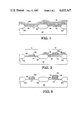
- FIGS. 1 through 7 are cross-sectional drawings showing an idealized sequence of process steps for select exemplary integrated circuit components having electrodes and interconnections formed by the method according to the present invention.
- the process of the present invention begins with a commercially available silicon wafer which defines a silicon substrate 10 for the integrated circuit being fabricated.
- the circuit components are constructed in accordance with well-known integrated circuit fabrication techniques.
- a section of an integrated circuit substrate 10 is shown with two such devices, one a single gate device 11 and the other a double gate device 13 as may be constructed, for example, for an EPROM cell.
- FIG. 1 shows the substrate 10 at the completion of several steps accomplished preparatory to forming transistor gates.
- An insulator layer (not shown) has been formed over the substrate 10; typically a silicon dioxide layer is formed by thermal oxidation of the substrate 10 in an oxidizing atmosphere at an elevated temperature. The thickness is not critical and is often in the range of 200 to 1,000 Angstroms.
- a layer of a different insulator, such as silicon nitride (not shown), is then formed, usually by chemical vapor deposition (CVD).
- a common photoresist mask technique is then used to create a pattern in the nitride. Thick isolating field oxide regions 22 are then grown.
- a gate oxide layer 12 is formed, again such as by thermal growth.
- a first polysilicon layer 14 is formed (aka Poly I) and patterned; an inter-gate oxide layer 16 is formed and patterned on polysilicon layer 14 above the region where the EPROM cell 13 is to be constructed and/or on the substrate 10, layer 17 is formed to be used for a single gate device 11; another polysilicon layer 18 is formed (aka Poly II); and a layer of silicon nitride 20 is formed.
- the nitride layer is commonly formed in a thickness having a range of 700 to 1500 Angstroms.
- Photoresist is then patterned using conventional photolithographic techniques and conventional plasma etching can be used to pattern the nitride 20 and the Poly II 18 as shown in FIG. 2.
- the interoxide layer 16 has been dipped out except between the Poly I 14 and the Poly II 18.
- Commonly known etching can be used to form a self-aligned floating gate 24 for the double gate EPROM structure 13.
- FIG. 4 illustrates the structure at step completion following the doping of regions of the substrate on each side of the single gate structure 26 and each side of the double gate structure 28 to form source and drain regions of the FETs 11, 13 in the substrate 10.
- the drain and source regions there is no physical distinction between the drain and source regions in a MOSFET because of the inherent symmetry of the structure. Rather, the biasing conditions generally determine which region is considered the source and which region is considered the drain.
- the source regions are designated 30 and the drain regions are designated 32 arbitrarily.
- the dopant ions most commonly used are arsenic or phosphorous ions; for a p-channel type MOSFET, the dopant ions most commonly used are boron ions.
- a common technique for forming the source 30 and drain 32 is ion implantation where the ions are introduced into the substrate 10 with an implant energy of approximately 30 to 150 kev to form impurity concentrations of about 10 20 atoms per cubic centimeter.
- the next step of the process is to grow thermally another oxide layer 34 on the surface of substrate 10 above the source 30 and drain 32 regions and around the sides of the gates 18, 24, 36.
- the thickness of this oxide layer is approximatley 500 to 1500 Angstroms.
- Hot phosphoric acid is then used to remove the remaining nitride layers 20 from the top surface of the gate 36 and the gate 18. Conventional methods are employed in these steps to achieve the structure as shown in FIG. 5.
- FIG. 6 The key to the present invention lies in the next fabrication steps represented in completion phase by FIG. 6.
- a thin film of titanium 40 is deposited across the top surface of the die, represented by the structure of FIG. 5.
- commercial sputtering equipment was used to obtain a film having a thickness of approximately 500 to 1500 Angstroms.
- the structure formed to this point in the process is then rapidly heated (within 30 seconds) to a temperature having a range of approximately 500 to 800 degrees centigrade.
- One method of rapidly raising the temperature is to subject the structure to the radiation of a tungsten halogen lamp in a non-oxidizing ambient atmosphere, such as argon.
- the structure is then allowed to bake for a time sufficient to allow the titanium to react with the underlying layer of polysilicon, viz. the gates 18,36. It has been determined that a period in the range of one to thirty seconds suffices to form a substantially homogeneous titantium silicide alloy layer 42 superposing the gate layers 18, 36.
- the titanium silicide gate electrodes 42 formed in accordance with this procedure have a sheet resistance of approximately one to five ohms per square.
- the areas of the surface of the structure coated with the thermal oxide of the previous steps are not converted during the baking to silicide.
- a layer of substantially pure titanium 40 remains as previously deposited.
- a standard ammonia hydroxide/hydrogen peroxide solution stripping of this titanium 40 can be readily accomplished.
- the sidewalls 44 of the thermal oxide 34 acts to reduce the thickness of the titanium on the sidewalls 44. This prevents silicon from moving out of the Poly I and Poly II lines during the heating and baking to form unwanted titanium silicide formations in the circuit, viz. other than as electrodes and interconnections as determined by the mask applied prior to the stripping. This clean edge definition is important to establishing optimal operational parameters for the entire integrated circuit device.
- Standard fabrication techniques can next be used to deposit standard remaining layers necessary to finalize the particular integrated circuit device, such as further insulation, metallization, and passivation layers.
- the method of the present invention also prevents holes from being left in the structure during the construction of these subsequent layers.
Abstract
Description
Claims (5)
Priority Applications (3)
| Application Number | Priority Date | Filing Date | Title |
|---|---|---|---|
| US06/717,370 US4635347A (en) | 1985-03-29 | 1985-03-29 | Method of fabricating titanium silicide gate electrodes and interconnections |
| EP86302334A EP0200364A1 (en) | 1985-03-29 | 1986-03-27 | Method of fabricating metal silicide gate electrodes and interconnections |
| JP61072381A JPS61230362A (en) | 1985-03-29 | 1986-03-28 | Making of titanium silicide gate electrode and mutual connection thereof |
Applications Claiming Priority (1)
| Application Number | Priority Date | Filing Date | Title |
|---|---|---|---|
| US06/717,370 US4635347A (en) | 1985-03-29 | 1985-03-29 | Method of fabricating titanium silicide gate electrodes and interconnections |
Publications (1)
| Publication Number | Publication Date |
|---|---|
| US4635347A true US4635347A (en) | 1987-01-13 |
Family
ID=24881756
Family Applications (1)
| Application Number | Title | Priority Date | Filing Date |
|---|---|---|---|
| US06/717,370 Expired - Lifetime US4635347A (en) | 1985-03-29 | 1985-03-29 | Method of fabricating titanium silicide gate electrodes and interconnections |
Country Status (3)
| Country | Link |
|---|---|
| US (1) | US4635347A (en) |
| EP (1) | EP0200364A1 (en) |
| JP (1) | JPS61230362A (en) |
Cited By (53)
| Publication number | Priority date | Publication date | Assignee | Title |
|---|---|---|---|---|
| US4690730A (en) * | 1986-03-07 | 1987-09-01 | Texas Instruments Incorporated | Oxide-capped titanium silicide formation |
| US4708770A (en) * | 1986-06-19 | 1987-11-24 | Lsi Logic Corporation | Planarized process for forming vias in silicon wafers |
| US4766088A (en) * | 1982-10-22 | 1988-08-23 | Ricoh Company, Ltd. | Method of making a memory device with polysilicon electrodes |
| US4816423A (en) * | 1987-05-01 | 1989-03-28 | Texas Instruments Incorporated | Bicmos process for forming shallow npn emitters and mosfet source/drains |
| US4821085A (en) * | 1985-05-01 | 1989-04-11 | Texas Instruments Incorporated | VLSI local interconnect structure |
| US4931411A (en) * | 1985-05-01 | 1990-06-05 | Texas Instruments Incorporated | Integrated circuit process with TiN-gate transistor |
| US4957777A (en) * | 1988-07-28 | 1990-09-18 | Massachusetts Institute Of Technology | Very low pressure chemical vapor deposition process for deposition of titanium silicide films |
| US4997777A (en) * | 1988-01-04 | 1991-03-05 | Philippe Boivin | Manufacturing process for an integrated circuit comprising double gate components |
| US5057447A (en) * | 1990-07-09 | 1991-10-15 | Texas Instruments Incorporated | Silicide/metal floating gate process |
| US5059546A (en) * | 1987-05-01 | 1991-10-22 | Texas Instruments Incorporated | BICMOS process for forming shallow NPN emitters and mosfet source/drains |
| US5059162A (en) * | 1989-10-03 | 1991-10-22 | Nissan Motor Co., Ltd. | Planetary gear system |
| US5095348A (en) * | 1989-10-02 | 1992-03-10 | Texas Instruments Incorporated | Semiconductor on insulator transistor |
| US5151375A (en) * | 1990-06-13 | 1992-09-29 | Waferscale Integration, Inc. | EPROM virtual ground array |
| US5158902A (en) * | 1989-04-28 | 1992-10-27 | Kabushiki Kaisha Toshiba | Method of manufacturing logic semiconductor device having non-volatile memory |
| US5166771A (en) * | 1990-01-12 | 1992-11-24 | Paradigm Technology, Inc. | Self-aligning contact and interconnect structure |
| US5188976A (en) * | 1990-07-13 | 1993-02-23 | Hitachi, Ltd. | Manufacturing method of non-volatile semiconductor memory device |
| US5204835A (en) * | 1990-06-13 | 1993-04-20 | Waferscale Integration Inc. | Eprom virtual ground array |
| US5208175A (en) * | 1990-12-21 | 1993-05-04 | Samsung Electronics Co., Ltd. | Method of making a nonvolatile semiconductor memory device |
| US5288666A (en) * | 1990-03-21 | 1994-02-22 | Ncr Corporation | Process for forming self-aligned titanium silicide by heating in an oxygen rich environment |
| US5327378A (en) * | 1992-03-04 | 1994-07-05 | Waferscale Integration, Inc. | Easily manufacturable compact EPROM |
| US5352620A (en) * | 1984-05-23 | 1994-10-04 | Hitachi, Ltd. | Method of making semiconductor device with memory cells and peripheral transistors |
| US5420060A (en) * | 1988-11-14 | 1995-05-30 | Texas Instruments Incorporated | Method of making contract-free floating-gate memory array with silicided buried bitlines and with single-step defined floating gates |
| US5432114A (en) * | 1994-10-24 | 1995-07-11 | Analog Devices, Inc. | Process for integration of gate dielectric layers having different parameters in an IGFET integrated circuit |
| US5443996A (en) * | 1990-05-14 | 1995-08-22 | At&T Global Information Solutions Company | Process for forming titanium silicide local interconnect |
| US5466622A (en) * | 1993-02-17 | 1995-11-14 | Sgs-Thomson Microelectronics, S.R.L. | Process for fabricating integrated devices including nonvolatile memories and transistors with tunnel oxide protection |
| US5470772A (en) * | 1991-11-06 | 1995-11-28 | Intel Corporation | Silicidation method for contactless EPROM related devices |
| US5472892A (en) * | 1992-07-31 | 1995-12-05 | Samsung Electronics Co., Ltd. | Method of making a non-volatile floating gate memory device with peripheral transistor |
| US5567642A (en) * | 1994-11-08 | 1996-10-22 | Hyundai Electronics Industries Co., Ltd. | Method of fabricating gate electrode of CMOS device |
| US5597748A (en) * | 1988-10-21 | 1997-01-28 | Kabushiki Kaisha Toshiba | Method of manufacturing NAND type EEPROM |
| US5656861A (en) * | 1990-01-12 | 1997-08-12 | Paradigm Technology, Inc. | Self-aligning contact and interconnect structure |
| US5656527A (en) * | 1990-09-22 | 1997-08-12 | Samsung Electronics Co., Ltd. | Method for fabricating a non-volatile semiconductor memory device having storage cell array and peripheral circuit, and a structure therefore |
| WO1997036332A1 (en) * | 1996-03-22 | 1997-10-02 | Philips Electronics N.V. | Floating gate non-volatile memory device, and a method of manufacturing the device |
| US5766997A (en) * | 1909-11-30 | 1998-06-16 | Nkk Corporation | Method of forming floating gate type non-volatile semiconductor memory device having silicided source and drain regions |
| US5766996A (en) * | 1994-11-21 | 1998-06-16 | Kabushiki Kaisha Toshiba | Method of manufacturing a semiconductor device |
| US5824560A (en) * | 1995-03-28 | 1998-10-20 | U.S. Philips Corporation | Method of manufacturing a semiconductor device with BICMOS circuit |
| US5862076A (en) * | 1990-11-13 | 1999-01-19 | Waferscale Integration, Inc. | Fast EPROM array |
| US5937325A (en) * | 1997-11-07 | 1999-08-10 | Advanced Micro Devices, Inc. | Formation of low resistivity titanium silicide gates in semiconductor integrated circuits |
| US5959892A (en) * | 1997-08-26 | 1999-09-28 | Macronix International Co., Ltd. | Apparatus and method for programming virtual ground EPROM array cell without disturbing adjacent cells |
| US5966605A (en) * | 1997-11-07 | 1999-10-12 | Advanced Micro Devices, Inc. | Reduction of poly depletion in semiconductor integrated circuits |
| US5972790A (en) * | 1995-06-09 | 1999-10-26 | Tokyo Electron Limited | Method for forming salicides |
| US6093593A (en) * | 1999-06-28 | 2000-07-25 | Taiwan Semiconductor Manufacturing Company | Method of forming a gate which provides a reduced corner recess in adjacent shallow trench isolation |
| US6187655B1 (en) | 1999-08-16 | 2001-02-13 | Taiwan Semiconductor Manufacturing Company | Method for performing a pre-amorphization implant (PAI) which provides reduced resist protect oxide damage and reduced junction leakage |
| US6197639B1 (en) * | 1998-07-13 | 2001-03-06 | Samsung Electronics Co., Ltd. | Method for manufacturing NOR-type flash memory device |
| US6255173B1 (en) | 1998-12-22 | 2001-07-03 | Hyundai Electronics Industries Co., Ltd. | Method of forming gate electrode with titanium polycide structure |
| US6284635B1 (en) | 1998-12-28 | 2001-09-04 | Hyundai Electronics Industries Co., Ltd. | Method for forming titanium polycide gate |
| US20010045605A1 (en) * | 1997-10-01 | 2001-11-29 | Katsura Miyashita | Semiconductor device comprising metal silicide films formed to cover gate electrode and source-drain diffusion layers and method of manufacturing the same |
| US6348389B1 (en) | 1999-03-11 | 2002-02-19 | Taiwan Semiconductor Manufacturing Company | Method of forming and etching a resist protect oxide layer including end-point etch |
| US6468914B1 (en) | 1998-12-29 | 2002-10-22 | Hyundai Electronics Industries Co., Ltd. | Method of forming gate electrode in semiconductor device |
| US6521959B2 (en) * | 1999-10-25 | 2003-02-18 | Samsung Electronics Co., Ltd. | SOI semiconductor integrated circuit for eliminating floating body effects in SOI MOSFETs and method of fabricating the same |
| US6544845B2 (en) * | 1997-03-05 | 2003-04-08 | Samsung Electronics Co., Ltd. | Methods of fabricating nonvolatile memory devices including bird's beak oxide |
| US20040089884A1 (en) * | 2000-12-29 | 2004-05-13 | Choo Kyo Seop | Thin film transistor array panel and method for fabricating the same |
| US20050224864A1 (en) * | 2003-03-19 | 2005-10-13 | Fujitsu Limited | Semiconductor device and its manufacture method |
| US20080213955A1 (en) * | 2005-07-01 | 2008-09-04 | Texas Instruments Incorporated | Schottky Diode With Minimal Vertical Current Flow |
Families Citing this family (7)
| Publication number | Priority date | Publication date | Assignee | Title |
|---|---|---|---|---|
| JP2633555B2 (en) * | 1987-03-23 | 1997-07-23 | 株式会社東芝 | Method for manufacturing semiconductor device |
| FR2658951B1 (en) * | 1990-02-23 | 1992-05-07 | Bonis Maurice | PROCESS FOR MANUFACTURING AN INTEGRATED CIRCUIT FOR A FAST ANALOGUE DIE USING LOCAL SILICIIDE INTERCONNECTION LINES. |
| US5185294A (en) * | 1991-11-22 | 1993-02-09 | International Business Machines Corporation | Boron out-diffused surface strap process |
| US5461005A (en) * | 1991-12-27 | 1995-10-24 | At&T Ipm Corp. | Method of forming silicide in integrated circuit manufacture |
| DE69832083D1 (en) * | 1998-12-29 | 2005-12-01 | St Microelectronics Srl | Selective silicidation process in nonvolatile semiconductor memories |
| JP4672217B2 (en) * | 2001-09-04 | 2011-04-20 | ルネサスエレクトロニクス株式会社 | Method for manufacturing nonvolatile semiconductor memory device |
| CN109192730A (en) * | 2018-09-18 | 2019-01-11 | 武汉新芯集成电路制造有限公司 | A kind of semiconductor devices and its manufacturing method |
Citations (12)
| Publication number | Priority date | Publication date | Assignee | Title |
|---|---|---|---|---|
| US3753774A (en) * | 1971-04-05 | 1973-08-21 | Rca Corp | Method for making an intermetallic contact to a semiconductor device |
| US4080719A (en) * | 1975-09-17 | 1978-03-28 | U.S. Philips Corporation | Method of manufacturing a semiconductor device and device manufactured according to the method |
| US4102733A (en) * | 1977-04-29 | 1978-07-25 | International Business Machines Corporation | Two and three mask process for IGFET fabrication |
| US4332839A (en) * | 1978-12-29 | 1982-06-01 | Bell Telephone Laboratories, Incorporated | Method for making integrated semiconductor circuit structure with formation of Ti or Ta silicide |
| US4356040A (en) * | 1980-05-02 | 1982-10-26 | Texas Instruments Incorporated | Semiconductor device having improved interlevel conductor insulation |
| US4443930A (en) * | 1982-11-30 | 1984-04-24 | Ncr Corporation | Manufacturing method of silicide gates and interconnects for integrated circuits |
| US4458410A (en) * | 1981-07-01 | 1984-07-10 | Hitachi, Ltd. | Method of forming electrode of semiconductor device |
| US4471524A (en) * | 1982-06-01 | 1984-09-18 | At&T Bell Laboratories | Method for manufacturing an insulated gate field effect transistor device |
| US4477310A (en) * | 1983-08-12 | 1984-10-16 | Tektronix, Inc. | Process for manufacturing MOS integrated circuit with improved method of forming refractory metal silicide areas |
| US4485550A (en) * | 1982-07-23 | 1984-12-04 | At&T Bell Laboratories | Fabrication of schottky-barrier MOS FETs |
| US4510670A (en) * | 1982-03-30 | 1985-04-16 | Siemens Aktiengesellschaft | Method for the manufacture of integrated MOS-field effect transistor circuits silicon gate technology having diffusion zones coated with silicide as low-impedance printed conductors |
| US4528744A (en) * | 1982-04-08 | 1985-07-16 | Tokyo Shibaura Denki Kabushiki Kaisha | Method of manufacturing a semiconductor device |
Family Cites Families (2)
| Publication number | Priority date | Publication date | Assignee | Title |
|---|---|---|---|---|
| GB2114809B (en) * | 1982-02-04 | 1986-02-05 | Standard Telephones Cables Ltd | Metallic silicide production |
| GB2139420B (en) * | 1983-05-05 | 1987-04-29 | Standard Telephones Cables Ltd | Semiconductor devices |
-
1985
- 1985-03-29 US US06/717,370 patent/US4635347A/en not_active Expired - Lifetime
-
1986
- 1986-03-27 EP EP86302334A patent/EP0200364A1/en not_active Withdrawn
- 1986-03-28 JP JP61072381A patent/JPS61230362A/en active Pending
Patent Citations (13)
| Publication number | Priority date | Publication date | Assignee | Title |
|---|---|---|---|---|
| US3753774A (en) * | 1971-04-05 | 1973-08-21 | Rca Corp | Method for making an intermetallic contact to a semiconductor device |
| US4080719A (en) * | 1975-09-17 | 1978-03-28 | U.S. Philips Corporation | Method of manufacturing a semiconductor device and device manufactured according to the method |
| US4102733A (en) * | 1977-04-29 | 1978-07-25 | International Business Machines Corporation | Two and three mask process for IGFET fabrication |
| US4332839A (en) * | 1978-12-29 | 1982-06-01 | Bell Telephone Laboratories, Incorporated | Method for making integrated semiconductor circuit structure with formation of Ti or Ta silicide |
| US4356040A (en) * | 1980-05-02 | 1982-10-26 | Texas Instruments Incorporated | Semiconductor device having improved interlevel conductor insulation |
| US4356040B1 (en) * | 1980-05-02 | 1991-12-10 | Texas Instruments Inc | |
| US4458410A (en) * | 1981-07-01 | 1984-07-10 | Hitachi, Ltd. | Method of forming electrode of semiconductor device |
| US4510670A (en) * | 1982-03-30 | 1985-04-16 | Siemens Aktiengesellschaft | Method for the manufacture of integrated MOS-field effect transistor circuits silicon gate technology having diffusion zones coated with silicide as low-impedance printed conductors |
| US4528744A (en) * | 1982-04-08 | 1985-07-16 | Tokyo Shibaura Denki Kabushiki Kaisha | Method of manufacturing a semiconductor device |
| US4471524A (en) * | 1982-06-01 | 1984-09-18 | At&T Bell Laboratories | Method for manufacturing an insulated gate field effect transistor device |
| US4485550A (en) * | 1982-07-23 | 1984-12-04 | At&T Bell Laboratories | Fabrication of schottky-barrier MOS FETs |
| US4443930A (en) * | 1982-11-30 | 1984-04-24 | Ncr Corporation | Manufacturing method of silicide gates and interconnects for integrated circuits |
| US4477310A (en) * | 1983-08-12 | 1984-10-16 | Tektronix, Inc. | Process for manufacturing MOS integrated circuit with improved method of forming refractory metal silicide areas |
Non-Patent Citations (6)
| Title |
|---|
| Choi et al., "Improved Salicide Process-Silicide Formation", I.B.M. Tech. Discl. Bull., vol. 27, No. 7B, Dec. 1984, pp. 4402-4404. |
| Choi et al., Improved Salicide Process Silicide Formation , I.B.M. Tech. Discl. Bull., vol. 27, No. 7B, Dec. 1984, pp. 4402 4404. * |
| Jones et al, "Salicide with Buried Silicide Layer", I.B.M. Tech. Discl. Bull., vol. 27, No. 2, Jul. 1984, pp. 1044-1045. |
| Jones et al, Salicide with Buried Silicide Layer , I.B.M. Tech. Discl. Bull., vol. 27, No. 2, Jul. 1984, pp. 1044 1045. * |
| Park et al., "Mo/Ti Bilayer Metallization-TiSi2 Process", J. Vac. Sci. Technol. A2(2) Apr.-Jun. 1984, pp. 259-263. |
| Park et al., Mo/Ti Bilayer Metallization TiSi 2 Process , J. Vac. Sci. Technol. A2(2) Apr. Jun. 1984, pp. 259 263. * |
Cited By (70)
| Publication number | Priority date | Publication date | Assignee | Title |
|---|---|---|---|---|
| US5766997A (en) * | 1909-11-30 | 1998-06-16 | Nkk Corporation | Method of forming floating gate type non-volatile semiconductor memory device having silicided source and drain regions |
| US4766088A (en) * | 1982-10-22 | 1988-08-23 | Ricoh Company, Ltd. | Method of making a memory device with polysilicon electrodes |
| US5352620A (en) * | 1984-05-23 | 1994-10-04 | Hitachi, Ltd. | Method of making semiconductor device with memory cells and peripheral transistors |
| US5302539A (en) * | 1985-05-01 | 1994-04-12 | Texas Instruments Incorporated | VLSI interconnect method and structure |
| US4821085A (en) * | 1985-05-01 | 1989-04-11 | Texas Instruments Incorporated | VLSI local interconnect structure |
| US4931411A (en) * | 1985-05-01 | 1990-06-05 | Texas Instruments Incorporated | Integrated circuit process with TiN-gate transistor |
| US4690730A (en) * | 1986-03-07 | 1987-09-01 | Texas Instruments Incorporated | Oxide-capped titanium silicide formation |
| US4708770A (en) * | 1986-06-19 | 1987-11-24 | Lsi Logic Corporation | Planarized process for forming vias in silicon wafers |
| WO1987007979A1 (en) * | 1986-06-19 | 1987-12-30 | Lsi Logic Corporation | Planarized process for forming vias in silicon wafers |
| US4816423A (en) * | 1987-05-01 | 1989-03-28 | Texas Instruments Incorporated | Bicmos process for forming shallow npn emitters and mosfet source/drains |
| US5059546A (en) * | 1987-05-01 | 1991-10-22 | Texas Instruments Incorporated | BICMOS process for forming shallow NPN emitters and mosfet source/drains |
| US4997777A (en) * | 1988-01-04 | 1991-03-05 | Philippe Boivin | Manufacturing process for an integrated circuit comprising double gate components |
| US4957777A (en) * | 1988-07-28 | 1990-09-18 | Massachusetts Institute Of Technology | Very low pressure chemical vapor deposition process for deposition of titanium silicide films |
| US5597748A (en) * | 1988-10-21 | 1997-01-28 | Kabushiki Kaisha Toshiba | Method of manufacturing NAND type EEPROM |
| US5824583A (en) * | 1988-10-21 | 1998-10-20 | Kabushiki Kaisha Toshiba | Non-volatile semiconductor memory and method of manufacturing the same |
| US5420060A (en) * | 1988-11-14 | 1995-05-30 | Texas Instruments Incorporated | Method of making contract-free floating-gate memory array with silicided buried bitlines and with single-step defined floating gates |
| US5158902A (en) * | 1989-04-28 | 1992-10-27 | Kabushiki Kaisha Toshiba | Method of manufacturing logic semiconductor device having non-volatile memory |
| US5095348A (en) * | 1989-10-02 | 1992-03-10 | Texas Instruments Incorporated | Semiconductor on insulator transistor |
| US5059162A (en) * | 1989-10-03 | 1991-10-22 | Nissan Motor Co., Ltd. | Planetary gear system |
| US5166771A (en) * | 1990-01-12 | 1992-11-24 | Paradigm Technology, Inc. | Self-aligning contact and interconnect structure |
| US5620919A (en) * | 1990-01-12 | 1997-04-15 | Paradigm Technology, Inc. | Methods for fabricating integrated circuits including openings to transistor regions |
| US5656861A (en) * | 1990-01-12 | 1997-08-12 | Paradigm Technology, Inc. | Self-aligning contact and interconnect structure |
| US5288666A (en) * | 1990-03-21 | 1994-02-22 | Ncr Corporation | Process for forming self-aligned titanium silicide by heating in an oxygen rich environment |
| US5443996A (en) * | 1990-05-14 | 1995-08-22 | At&T Global Information Solutions Company | Process for forming titanium silicide local interconnect |
| US5151375A (en) * | 1990-06-13 | 1992-09-29 | Waferscale Integration, Inc. | EPROM virtual ground array |
| US5204835A (en) * | 1990-06-13 | 1993-04-20 | Waferscale Integration Inc. | Eprom virtual ground array |
| US5057447A (en) * | 1990-07-09 | 1991-10-15 | Texas Instruments Incorporated | Silicide/metal floating gate process |
| US5188976A (en) * | 1990-07-13 | 1993-02-23 | Hitachi, Ltd. | Manufacturing method of non-volatile semiconductor memory device |
| US5656527A (en) * | 1990-09-22 | 1997-08-12 | Samsung Electronics Co., Ltd. | Method for fabricating a non-volatile semiconductor memory device having storage cell array and peripheral circuit, and a structure therefore |
| US5862076A (en) * | 1990-11-13 | 1999-01-19 | Waferscale Integration, Inc. | Fast EPROM array |
| US5208175A (en) * | 1990-12-21 | 1993-05-04 | Samsung Electronics Co., Ltd. | Method of making a nonvolatile semiconductor memory device |
| US5470772A (en) * | 1991-11-06 | 1995-11-28 | Intel Corporation | Silicidation method for contactless EPROM related devices |
| US5327378A (en) * | 1992-03-04 | 1994-07-05 | Waferscale Integration, Inc. | Easily manufacturable compact EPROM |
| US5472892A (en) * | 1992-07-31 | 1995-12-05 | Samsung Electronics Co., Ltd. | Method of making a non-volatile floating gate memory device with peripheral transistor |
| US5913120A (en) * | 1993-02-17 | 1999-06-15 | Sgs-Thomson Microelectronics S.R.L. | Process for fabricating integrated devices including nonvolatile memories and transistors with tunnel oxide protection |
| US5466622A (en) * | 1993-02-17 | 1995-11-14 | Sgs-Thomson Microelectronics, S.R.L. | Process for fabricating integrated devices including nonvolatile memories and transistors with tunnel oxide protection |
| US5432114A (en) * | 1994-10-24 | 1995-07-11 | Analog Devices, Inc. | Process for integration of gate dielectric layers having different parameters in an IGFET integrated circuit |
| US5567642A (en) * | 1994-11-08 | 1996-10-22 | Hyundai Electronics Industries Co., Ltd. | Method of fabricating gate electrode of CMOS device |
| US5766996A (en) * | 1994-11-21 | 1998-06-16 | Kabushiki Kaisha Toshiba | Method of manufacturing a semiconductor device |
| US5824560A (en) * | 1995-03-28 | 1998-10-20 | U.S. Philips Corporation | Method of manufacturing a semiconductor device with BICMOS circuit |
| US5972790A (en) * | 1995-06-09 | 1999-10-26 | Tokyo Electron Limited | Method for forming salicides |
| WO1997036332A1 (en) * | 1996-03-22 | 1997-10-02 | Philips Electronics N.V. | Floating gate non-volatile memory device, and a method of manufacturing the device |
| US5879990A (en) * | 1996-03-22 | 1999-03-09 | U.S. Philips Corporation | Semiconductor device having an embedded non-volatile memory and method of manufacturing such a semicondutor device |
| US6544845B2 (en) * | 1997-03-05 | 2003-04-08 | Samsung Electronics Co., Ltd. | Methods of fabricating nonvolatile memory devices including bird's beak oxide |
| US5959892A (en) * | 1997-08-26 | 1999-09-28 | Macronix International Co., Ltd. | Apparatus and method for programming virtual ground EPROM array cell without disturbing adjacent cells |
| US20050158958A1 (en) * | 1997-10-01 | 2005-07-21 | Kabushiki Kaisha Toshiba | Semiconductor device comprising metal silicide films formed to cover gate electrode and source-drain diffusion layers and method of manufacturing the same |
| US7638432B2 (en) | 1997-10-01 | 2009-12-29 | Kabushiki Kaisha Toshiba | Semiconductor device comprising metal silicide films formed to cover gate electrode and source-drain diffusion layers and method of manufacturing the same |
| US20070194382A1 (en) * | 1997-10-01 | 2007-08-23 | Kabushiki Kaisha Toshiba | Semiconductor device comprising metal silicide films formed to cover gate electrode and source-drain diffusion layers and method of manufacturing the same |
| US7220672B2 (en) | 1997-10-01 | 2007-05-22 | Kabushiki Kaisha Toshiba | Semiconductor device comprising metal silicide films formed to cover gate electrode and source-drain diffusion layers and method of manufacturing the same |
| US6869867B2 (en) * | 1997-10-01 | 2005-03-22 | Kabushiki Kaisha Toshiba | Semiconductor device comprising metal silicide films formed to cover gate electrode and source-drain diffusion layers and method of manufacturing the same wherein the silicide on gate is thicker than on source-drain |
| US20010045605A1 (en) * | 1997-10-01 | 2001-11-29 | Katsura Miyashita | Semiconductor device comprising metal silicide films formed to cover gate electrode and source-drain diffusion layers and method of manufacturing the same |
| US5937325A (en) * | 1997-11-07 | 1999-08-10 | Advanced Micro Devices, Inc. | Formation of low resistivity titanium silicide gates in semiconductor integrated circuits |
| US5966605A (en) * | 1997-11-07 | 1999-10-12 | Advanced Micro Devices, Inc. | Reduction of poly depletion in semiconductor integrated circuits |
| US6197639B1 (en) * | 1998-07-13 | 2001-03-06 | Samsung Electronics Co., Ltd. | Method for manufacturing NOR-type flash memory device |
| US6255173B1 (en) | 1998-12-22 | 2001-07-03 | Hyundai Electronics Industries Co., Ltd. | Method of forming gate electrode with titanium polycide structure |
| US6284635B1 (en) | 1998-12-28 | 2001-09-04 | Hyundai Electronics Industries Co., Ltd. | Method for forming titanium polycide gate |
| US6468914B1 (en) | 1998-12-29 | 2002-10-22 | Hyundai Electronics Industries Co., Ltd. | Method of forming gate electrode in semiconductor device |
| US6348389B1 (en) | 1999-03-11 | 2002-02-19 | Taiwan Semiconductor Manufacturing Company | Method of forming and etching a resist protect oxide layer including end-point etch |
| US6093593A (en) * | 1999-06-28 | 2000-07-25 | Taiwan Semiconductor Manufacturing Company | Method of forming a gate which provides a reduced corner recess in adjacent shallow trench isolation |
| US6187655B1 (en) | 1999-08-16 | 2001-02-13 | Taiwan Semiconductor Manufacturing Company | Method for performing a pre-amorphization implant (PAI) which provides reduced resist protect oxide damage and reduced junction leakage |
| US6703280B2 (en) * | 1999-10-25 | 2004-03-09 | Samsung Electronics Co., Ltd. | SOI semiconductor integrated circuit for eliminating floating body effects in SOI MOSFETs and method of fabricating the same |
| US6521959B2 (en) * | 1999-10-25 | 2003-02-18 | Samsung Electronics Co., Ltd. | SOI semiconductor integrated circuit for eliminating floating body effects in SOI MOSFETs and method of fabricating the same |
| US20040089884A1 (en) * | 2000-12-29 | 2004-05-13 | Choo Kyo Seop | Thin film transistor array panel and method for fabricating the same |
| US7679084B2 (en) * | 2000-12-29 | 2010-03-16 | Lg Display Co., Ltd. | Thin film transistor array panel and method for fabricating the same |
| US8304310B2 (en) | 2003-03-19 | 2012-11-06 | Fujitsu Semiconductor Limited | Manufacture method of semiconductor device |
| US20100096684A1 (en) * | 2003-03-19 | 2010-04-22 | Fujitsu Microelectronics Limited | Semiconductor device and its manufacture method |
| US20110136312A1 (en) * | 2003-03-19 | 2011-06-09 | Fujitsu Semiconductor Limited | Semiconductor device and its manufacture method |
| US20050224864A1 (en) * | 2003-03-19 | 2005-10-13 | Fujitsu Limited | Semiconductor device and its manufacture method |
| US20080213955A1 (en) * | 2005-07-01 | 2008-09-04 | Texas Instruments Incorporated | Schottky Diode With Minimal Vertical Current Flow |
| US8030155B2 (en) * | 2005-07-01 | 2011-10-04 | Texas Instruments Incorporated | Schottky diode with minimal vertical current flow |
Also Published As
| Publication number | Publication date |
|---|---|
| EP0200364A1 (en) | 1986-11-05 |
| JPS61230362A (en) | 1986-10-14 |
Similar Documents
| Publication | Publication Date | Title |
|---|---|---|
| US4635347A (en) | Method of fabricating titanium silicide gate electrodes and interconnections | |
| JP2857006B2 (en) | Self-aligned cobalt silicide on MOS integrated circuits. | |
| US4392150A (en) | MOS Integrated circuit having refractory metal or metal silicide interconnect layer | |
| US5605848A (en) | Dual ion implantation process for gate oxide improvement | |
| US5476802A (en) | Method for forming an insulated gate field effect transistor | |
| US5451545A (en) | Process for forming stable local interconnect/active area silicide structure VLSI applications | |
| US5652156A (en) | Layered polysilicon deposition method | |
| US4735680A (en) | Method for the self-aligned silicide formation in IC fabrication | |
| US4149307A (en) | Process for fabricating insulated-gate field-effect transistors with self-aligned contacts | |
| EP0322244A2 (en) | Self-limiting mask undercut process | |
| US4743564A (en) | Method for manufacturing a complementary MOS type semiconductor device | |
| EP0126424A2 (en) | Process for making polycide structures | |
| GB2140619A (en) | Fabrication of fet's | |
| EP0322243A2 (en) | Process of manufacture of a gallium arsenide field effect transistor | |
| US5286678A (en) | Single step salicidation process | |
| KR20000041393A (en) | Method of manufacturing gate electrode of semiconductor device | |
| US4900690A (en) | MOS semiconductor process with double-layer gate electrode structure | |
| JPH08116057A (en) | Manufacture of tin gate electrode on semiconductor device | |
| US4216573A (en) | Three mask process for making field effect transistors | |
| JPH05226361A (en) | Field effect transistor | |
| JP4730993B2 (en) | Method for forming conductive line of semiconductor element | |
| JPH1064898A (en) | Manufacturing method of semiconductor device | |
| JP3196241B2 (en) | Method for manufacturing semiconductor device | |
| JPH0362300B2 (en) | ||
| KR100238872B1 (en) | Method of manufacturing semiconductor device |
Legal Events
| Date | Code | Title | Description |
|---|---|---|---|
| AS | Assignment |
Owner name: ADVANCED MICRO DEVICES, INC., 901 THOMPSON PLACE, Free format text: ASSIGNMENT OF ASSIGNORS INTEREST.;ASSIGNORS:LIEN, JIH-CHANG;WANG, HSINGYA A.;REEL/FRAME:004392/0940 Effective date: 19850329 |
|
| STCF | Information on status: patent grant |
Free format text: PATENTED CASE |
|
| FPAY | Fee payment |
Year of fee payment: 4 |
|
| FPAY | Fee payment |
Year of fee payment: 8 |
|
| FPAY | Fee payment |
Year of fee payment: 12 |
|
| AS | Assignment |
Owner name: GLOBALFOUNDRIES INC., CAYMAN ISLANDS Free format text: AFFIRMATION OF PATENT ASSIGNMENT;ASSIGNOR:ADVANCED MICRO DEVICES, INC.;REEL/FRAME:023119/0083 Effective date: 20090630 |
|
| AS | Assignment |
Owner name: GLOBALFOUNDRIES U.S. INC., NEW YORK Free format text: RELEASE BY SECURED PARTY;ASSIGNOR:WILMINGTON TRUST, NATIONAL ASSOCIATION;REEL/FRAME:056987/0001 Effective date: 20201117 |