US4553233A - Multiple-ring communication system - Google Patents
Multiple-ring communication system Download PDFInfo
- Publication number
- US4553233A US4553233A US06/562,133 US56213383A US4553233A US 4553233 A US4553233 A US 4553233A US 56213383 A US56213383 A US 56213383A US 4553233 A US4553233 A US 4553233A
- Authority
- US
- United States
- Prior art keywords
- ring
- node
- test
- transmitter
- receiver
- Prior art date
- Legal status (The legal status is an assumption and is not a legal conclusion. Google has not performed a legal analysis and makes no representation as to the accuracy of the status listed.)
- Expired - Lifetime
Links
Images

Classifications
-
- H—ELECTRICITY
- H04—ELECTRIC COMMUNICATION TECHNIQUE
- H04L—TRANSMISSION OF DIGITAL INFORMATION, e.g. TELEGRAPHIC COMMUNICATION
- H04L12/00—Data switching networks
- H04L12/28—Data switching networks characterised by path configuration, e.g. LAN [Local Area Networks] or WAN [Wide Area Networks]
- H04L12/42—Loop networks
- H04L12/437—Ring fault isolation or reconfiguration
-
- H—ELECTRICITY
- H04—ELECTRIC COMMUNICATION TECHNIQUE
- H04B—TRANSMISSION
- H04B1/00—Details of transmission systems, not covered by a single one of groups H04B3/00 - H04B13/00; Details of transmission systems not characterised by the medium used for transmission
- H04B1/74—Details of transmission systems, not covered by a single one of groups H04B3/00 - H04B13/00; Details of transmission systems not characterised by the medium used for transmission for increasing reliability, e.g. using redundant or spare channels or apparatus
- H04B1/745—Details of transmission systems, not covered by a single one of groups H04B3/00 - H04B13/00; Details of transmission systems not characterised by the medium used for transmission for increasing reliability, e.g. using redundant or spare channels or apparatus using by-passing or self-healing methods
Definitions
- the present invention relates to a multiple-ring communication system which includes a plurality of nodes intercoupled in at least two rings and operating on an equal basis without central control, each node including a plurality of message receiver/transmitter equipments associated to distinct ones of said rings respectively and able to receive messages on said rings and transmit messages thereon in opposite directions, and processing means for checking the receipt or absence of receipt of signals on the receiver ring portions connecting the receivers of said node to transmitters of its neighbouring nodes and for performing reconfiguration operations in response to the result provided by said checking operation.
- DDLCN distributed double-loop computer network
- Such a reconfiguration measure consists for instance in case of an interruption for both rings, in transforming the double ring system into a single ring system by establishing two interconnections between these rings.
- each node transmits to its neighbouring nodes timing signals as long as it is not transmitting messages, so that each node receives such timing signals substantially in a continuous way on the receiver ring portions by means of which its receivers are coupled to the transmitters of the neighbouring nodes.
- Each node tests the condition of its neighbouring nodes by checking the receipt or absence of receipt of these timing signals. In this way very limited information is obtained at the testing node on the overall status of the system since this information only concerns the condition of the receiver ring portions, of the transmitters of the neighbouring nodes and of the own receivers.
- An object of the present invention is to provide a multiple-ring communication system of the above type, but each node of which is adapted to collect more information on the status of the system.
- this object is achieved due to the fact that said receiver/transmitter equipments of each said node are able to transmit on said rings ring test messages the destination of which is said node itself, said processing means controlling said receiver/transmitter equipments of said node and being able to check the receipt or absence of receipt of said ring test messages prior to possibly executing said reconfiguration operations.
- each node By checking the receipt or absence of receipt of the ring test messages information is obtained on the condition of all the nodes and of all the ring portions interconnecting these nodes. Thus each node always knows if one or both rings are operating correctly or not and if loops have been established between these rings or not.
- receiver/transmitter equipments of each said node are also able to transmit on said rings neighbouring node test messages which upon receipt by receiver/transmitter equipments of said neighbouring nodes normally give rise to the transmission to said node of node test reply messages on rings different from those on which said neighbouring node test messages were transmitted, said processing means being also able to check the receipt or absence of receipt of said test reply messages prior to possibly executing said reconfiguration operations.
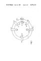
- FIG. 1 shows a multiple-ring communication system according to the invention
- FIG. 2 represents a station or node N1 and associated user circuits G1 of FIG. 1 in more detail.
- the multiple-ring communication system shown in FIG. 1 is more particularly a double-ring system which includes a plurality of stations or nodes N1 totaling Nn which are intercoupled so as to form two communication loops or rings RG1 and RG2 and which operate on an equal basis without central control.
- the system operates in a plesochronous way, meaning that each node is operating at the rhythm of its own clock but that the frequency difference between the clocks of all nodes is restricted to a predetermined value.
- Such a way of operation is generally known in the technique e.g. in packet switching networks.
- RG1 and RG2 messages are able to be transmitted in opposite directions as indicated by the arrows and in each node a message receiver and a message transmitter are connected to each of the rings, e.g. in N1, R11 and T11 are connected to RG1 and R12 and T12 are connected to RG2.
- the nodes N1 to Nn have access to groups of user terminal circuits G1 to Gn respectively.
- Node N1 represented in FIG. 2 is identical to all other nodes and includes equipment associated in common to both the rings RG1 and RG2 as well as equipment individually associated to each of these rings.
- the common equipment of node N1 includes:
- main processor MP1 e.g. 8086 INTEL processor, having access to an individually associated memory MEM1 including a system status register SSR and to a common communication bus BB1;
- auxiliary processors AP100 to AP115 having access to the common bus BB1 and to individually associated sets of user terminal circuits S1OO to S115 respectively. These sets together form the above mentioned group G1.
- the equipment of node N1 individually associated to ring RG1 includes;
- a receiver processing unit RPU11 directly coupled to receiver R11 and a transmitter processing unit TPU11 coupled to transmitter T11 via a change-over switch SW11 which will be considered later;
- a delay buffer constituted by a first-in-first-out or FIFO circuit FIFO11 coupling RPU11 to TPU11;
- a control register CR11 coupled to the latter bus BB1 via control lead c111 and storing a so-called "faulty side bit" FSB11.
- This bit is 0 or 1 depending on N1 at the side looking in the direction of RG1 (FIG. 1) being not faulty or faulty respectively.
- This side includes portions of RG1 and RG2 and node N2.
- the equipment individually associated to ring RG2 includes a receiver R12, a transmitter T12, a receiver processing unit RPU12, a transmitter processing unit TPU12; a change-over switch SW12, a delay buffer or FIFO circuit FIDO2; an input buffer or receiver memory RM12, an output buffer or transmitter memory TM12 and a control register CR12 coupled to bus BB1 via control leads c112 and c113 and storing not only a malicious side bit FSB12 but also a socalled transparency bit TPB12. All these circuits are interconnected in the same way as the corresponding circuits of the equipment individually associated to RG1.
- FSB12 is 0 or 1 depending on the side of N2 looking in the direction of RG2 (FIG.
- Transparency bit TPB12 is associated to ring RG2 i.e. to RPU12 and is 1 or 0 depending on N1 being transparent or not respectively with respect to RG2 as will be explained later.
- Change-over switch SW11 enables either TPU11 or TPU12 to be connected to T11 and change-over switch SW12 likewise enables either TPU11 or TPU12 to be connected to T12.
- Each of these switches SW11 and SW12 is in fact a well known 2-input-1-output digital multiplexer further having a select input.
- the select inputs of these multiplexers are controlled by FSB12 and FSB11 stored in the control registers CR12 and CR11 respectively. Depending on FSB12 being 0 or 1, the output of TPU11 or TPU12 is connected to T11 and depending on FSB11 being 0 or 1, the output of TPU12 or TPU11 is connected to T12.
- FSB12 FSB11
- receiver R12 R11
- transmitter T12 T11
- T11 T11
- T12 T12
- RG1 RG2
- Functions of the main processor MP1 are, amongst others, to collect via the bus BB1 messages transmitted by RM11, RM12 and the auxiliary processors AP100-AP115, to process these messages, to form new messages and store them via bus BB1 in TM11 or TM12 for subsequent transmission to another node, to set or reset the bits FSB11, FSB12, TMB12 via BB1 and c111, c112, c113 respectively, to transmit messages to the auxiliary processors via BB1, and to perform time-outs.
- the auxiliary processors AP100-AP115 are able, for instance, to process messages incoming from MP1 via BB1 and from the associated sets of user terminal circuits S100-S115. They also can transmit messages to MP1 and to S100-S115.
- the receiver processing circuits RPU11 and RPU12 are able to execute relatively simple functions such as processing the messages received in R11, R12 on RG1, RG2 and storing them either in RM11, RM12 (thus removing them from the ring) or in FIFO11, FIFO12 (for transmission to another node) depending on the type of message.
- a message can only be removed from the ring by the originating node and by the destination node.
- the transmitter processing units TPU11 and TPU12 are able to execute relatively simple functions such as processing the messages stored in TM11, TM12 or in FIFO11, FIFO12 and operating T11, T12 or T12, T11, depending on the condition of FSB11, FSB12, in order to transmit these messages on RG1, RG2 or RG2, RG1.
- the messages used in the present system for testing it are the following:
- ring test messages which are intended for testing the ring RG1 and RG2. They are transmitted in each node on RG1 and RG2 and removed from the ring when received back in this node. If everything is o.k. this happens after the message has passed through all the other nodes via RG1 or RG2. It is clear that when a ring test message is received back in a node this is an indication that the receiver/transmitter equipments, associated to this ring, of all the nodes operate correctly and that the portions of the ring interconnecting these nodes are not faulty;
- adjacent-node test messages which are intended mainly for testing the adjacent nodes of each node. They are transmitted in each node on RG1 or RG2;
- adjacent-node test reply messages which are also mainly intended for testing the adjacent nodes of a node as they are transmitted from these adjacent nodes to the latter node in reply to adjacent-node test messages. This transmission is performed on rings different from those on which the adjacent-node test messages were received by the node. Hence, when an adjacent node test reply message is received in a node from an adjacent node this is an indication that the receiver/transmitter equipments involved in the operation of both nodes and the ring portions interconnecting these nodes are not faulty.
- adjacent-node test and the adjacent-node test reply messages are called node test and node test reply messages for simplicity reasons.
- the equipment of node N1 is able to transmit two ring test messages RTM11 (message from N1 on RG1) and RTM12 (message from N1 on RG2) and two node test messages NTM11 (message from N1 on RG1) and NTM12 (message from N1 on RG2) and to receive from the adjacent nodes N2 and Nn in rep1y to these node test messages two node test reply messages NTRM22 (message from N2 on RG2) and NTRMn1 (message from Nn on RG1).
- the node N1 is also able to transmit node test reply messages NTRM11 and NTRM12 to N2 and Nn respectively, but this is without importance for the further description.
- the above test messages may contain:
- a ring identifier for identifying the ring on which the message is transmitted
- information related to the message type e.g. an indication that upon the message being received on a ring a reply message should be transmitted on the other ring. If there are more than two rings the identity of this other ring should be given.
- the ring test messages RTM11 and RTM12 contain the following information:
- ring identifier RG1 and RG2 respectively.
- the node test messages NTM11 and NTM12 contain the following information:
- ring identifier RG1 and RG2 respectively;
- the main processor indicating that upon the receipt of the message by a node on a ring a reply message should be transmitted on the other ring to the source node of the message.
- the information can also contain an indication that upon the receipt of the message a test programme should be started and that a reply message should be transmitted to the source node of the test message on the other ring only when the test was successful.
- the node test message does not contain a destination address, i.e. the address of an adjacent node. In this way, each node can be perfectly unaware of the structure of the ring and more particularly has not to know the identity of its neighbouring nodes. Thus the structure of the ring can be modified without it being necessary to adapt the messages.
- the node test reply messages NTRM22 and NTRMn1 contain the following information:
- ring identifier RG2 and RG1 respectively.
- each message and hence each of the test messages RTM11, NTRMn1 (RTM12, NTRM22) received by R11 (R12) is processed by RPU11 (RPU12) and stored in RM11 (RM12) or in FIFO11 (FIFO12) depending on the message being intended for node N1 or for another node respectively;
- a received message which has been stored in RM11 (RM12) is processed by MP1 and possibly transmitted to an auxiliary processor AP100-AP115 where it is further processed and possibly sent from there to one of the user terminal circuits of the associated set S100-S1115 respectively;
- a received message which has been stored in FIFO11 is processed by TPU11 and transmitted on RG1 (RG2) by transmitter T11 (T12) if FSB12 (FSB11) is 0. However, if FSB12 (FSB11) is 1 this message is transmitted on RG2 (RG1) by transmitter T12 (T11);
- a message which has been locally formed by MP1 and has to be transmitted to another node such as the test messages RTM11, RTM12, NTM11, NTM12, is stored by MP1 either in TM11 or in TM12 and then handled by TPU11 or TPU12 in a similar way as the messages stored in FIFO11 and FIFO12.
- the equipment corresponding to the following equipment in N1 R11, RPU11, FIFO11, TPU11, SW11, T11 and R12, RPU12, FIFO12, TPU12, SW12, T12;
- N2 and Nn the equipments corresponding to the following receiving equipments in N1: R11, RPU11, RM11, MP1, MEM1; and R12, RPU12, RM12, MP1, MEM1 rsspectively.
- the transmission equipment corresponding to the following transmission equipments in N1 MP1, MEM1, TM12, TPU12, SW12, T12; and MP1, MEM1, TM11, TPU11, SW11, T11 respectively
- main processor MP1 is more particularly able to control the following functions:
- a maintenance system (not shown), e.g. to indicate that RG1 or RG2 is O.K. or faulty;
- SSR shown in columns 2 to 5 of the table on the last page of the description. SSR indicates the status of the system as seen in node N1. It more particularly has four successive locations for registering the reaction detected in node N1 to the transmission of RTM11, RTM12, NTM11 and NTM12 respectively. This reaction is one of the following codes:
- the codes 00 to 11 are not shown in the SSR.
- Main processor MP1 alternately counts time intervals TO1 and TO2.
- TO1 normal messages are transmitted and no tests are performed, whilst during TO2 only ring test messages RTM11 and RTM12 and node test messages NTM11 and NTM12 are transmitted.
- the receipt or absence of receipt of the ring test messages as well as of the node test reply messages NTRM22 and NTRMn1 is checked and their possible receipt is registered in the system status register SSR.
- these test messages are received before the end of TO2 at which moment the processor MP1 evaluates the result of the tests by checking the contents of SSR. In function of this result the MP1 then decides to execute measures to reconfigure a faulty system back to a correctly operating system to inform a maintenance system (not shown), or to do nothing.
- the main processor MP1 After the end of a time interval TO1, the main processor MP1:
- the transmitter processing units TPU11 and TPU12 then first read the ring test messages RTM11 and RTM12 and operate T11 and T12 to transmit these messages on RG1 and RG2 respectively. Immediately afterwards and in an analogous way the node test messages NTM11 and NTM12 are read and transmitted on RG1 and RG2 respectively.
- the ring test message RTM11 on RG1 is successively received and transmitted by the nodes N2 to Nn and finally received by node N1, and the ring test message RTM12 on RG2 is successively received and transmitted by the nodes Nn to N2 and finally received by N1.
- a ring test message RTM11, RTM12 is received by a receiver of one of the nodes N2 to Nn the receiver processing unit associated to this receiver derives from the contents of the message that its destination is node N1 and therefore writes the ring test message in the associated FIFO.
- the processing unit associated to this FIFO starts reading it as soon as e.g. a byte of this message has been stored in the FIFO and then operates the associated transmitter to transmit it on the associated ring.
- the following bytes of the message are transmitted in the same way.
- the node test messages NTM11 and NTM12 transmitted on the rings RG1 and RG2 are received by the receivers associated to RG1 and RG2 of the neighbouring nodes N2 and Nn respectively.
- the receiver processing unit associated to each of these receivers derives from the contents of the message received that it is a node test message and therefore stores it in the associated memory or input buffer. Thus the node test message is removed from the ring.
- each of the main processors of the nodes N2 and Nn afterwards reads the node test message from this memory it forms a node test reply message, NTRM22 and NTRMn1 respectively, and stores it in the transmitter memory associated to the ring, RG2 and RG1 respectively, for transmission on this ring.
- node test reply messages NTRM22 and NTRMn1 are received by the receivers R12 and R11 of node N1 and then stored in RM12 and RM11 by RPU12 and RPU11 respectively. Thus they are removed from the rings RG1 and RG2.
- the main processor MP1 Each time a ring test message or a node test reply message is received in one of the receiver memories RM11 and RM12, the main processor MP1 updates its system status register SSR.
- the processor MP1 upon receiving such a message knows if it is received on the ring on which it was originally transmitted or not since the ring on which it is received is that associated to the memory RM11, RM12 in which the received message is stored, whilst the ring on which it was transmitted is given by the ring identifier of the message.
- the ring test messages RTM11 and RTM12 as well as the node test reply messages NTRM21 and NTRMn1 are received in node N1 before the end of the time interval TO2 on the rings RG1, RG2, RG2 and RG1 respectively. This is not so if one or more nodes and/or one or more ring portions between these nodes are faulty.
- the above mentioned table lists the various possible contents of the SSR which may be found in node N1 at the end of a time interval TO2 following the transmission of the ring test messages RTM11 and RTM12 and of the node test messages NTM11 and NTM12.
- X means either N or NTRM22
- Y means either N or NTRMn1.
- ring RG1 is OK, NOK respectively;
- ring RG2 is OK, NOK respectively;
- N2D, NnD adjacent node N2, Nn is not operative or down, e.g. power down.
- This condition includes the condition of the node N2, Nn and/or the ring portions between N2, Nn and N1;
- N2O, NnO adjacent node N2, Nn is on-line, but not active, e.g. during programme loading;
- N2A, NnA adjacent node N2, Nn is active. This also includes the node N2, Nn and the ring portions between N2, Nn and N1;
- NRG1, NRG2 in a node able to be reached from node N1 via RG1, RG2 a loop has been established, between RG1 and RG2 or between RG2 and RG1 respectively.
- the main processor MP1 possibly controls the execution of reconfiguration operations in node N1 by setting to 1 one or more of the bits FSB11, FSB12 and TPB12.
- RTM11 and RTM12 are received back in N1 on RG1 and RG2 respectively.
- the main processor MP1 Independently from the receipt or absence of receipt of NTRM22 or NTRMn1, as indicated by X or Y, the main processor MP1 deduces from this information that in the system both the rings RG1 and RG2 are O.K. and decides therefore that no reconfiguration measures have to be taken. It also sends a message to the maintenance system to inform it of the fact that both the rings are O.K.
- RTM11 and RTM12 are received back in N1 on RG2 and RG1 as indicated by RTM'11 and RTM'12 respectively.
- the main processor MP1 Independently from the reception or absence of reception of NTRM22 or NTRMn1, as indicated by X or Y, the main processor MP1 deduces from this information that RG1 and RG2 are both interrupted somewhere, e.g. in Z on FIG. 1, but that, as indicated by NRG1 and NRG2 in nodes Nx and Nn-1 (FIG. 1) able to be reached from N1 via RG1 and RG2 loops Lx and Ln-1 have been established between RG1 and RG2 and between RG2 and RG1 respectively so that a new single ring has been formed.
- MP1 then only transmits test messages and sets to 1 the transparency bit TPB12 which makes RG2 in Nn transparent by bringing RPU12 in such a condition that all messages, except node test reply messages, received by R12 are stored in FIFO12 for further transmission by T12 on RG2.
- Node test reply messages are stored in RM12.
- Making RG2 transparent in N1 in the case two loops, such as Lx and Ln-1, have been formed is necessary because--as mentioned above-- messages may be removed from a ring either by the node which originated the message or by the node of destination.
- RTM11 is received back in N1 on RG2, as indicated by RTM'11, and RTM12 is not received back in N1, NTRM22 and NTRMn1 are either received or not.
- the main processor MP1 deduces the system status SS as follows :
- RG1 is interrupted somewhere but that in some node able to be reached via RG1 a loop has been established between RG1 and RG2. This is indicated by NRG1;
- N2 or NnA is active. This is indicated by N2A or NnA;
- N2D or Nnd is down. This is indicated by N2D or Nnd;
- MP1 decides to set to 1 both FSB11 and FSB12 for the cases 5 and 7 and to do nothing for the cases 6 and 8.
- FSB11 By setting FSB11 to 1 a loop is established between R11 and T12, i.e. between RG1 and RG2, whilst by setting FSB12 to 1 a loop is established between R12 and T11, i.e. between RG2 and RG1.
- the latter loop is required to permit messages received from N2 by R12 to be transmitted back to N2, whilst the former loop enables messages sent by Nn after it is no longer down to be transmitted to N1 and received back therefrom and to prevent such messages from being transmitted by T11.
- cases 6 and 8 are unstable cases because as RG2 is somewhere interrupted a loop will somewhere be formed between RG2 and RG1 in which case also RTM12 will be received on another ring as RTM'12 (see case 4).
- RTM11 and RTM12 are not received back in N1 and NTRM22 and NTRMn1 are either received or not so that the system status for the cases 13 to 16 is similar to that of cases 5 to 8 respectively, except for NRG1 which now does not form part of the status and for N20 which is replaced by N2D. Also the reconfiguration measures for the cases 13 to 15 are identical to those for the cases 5 to 7. However for case 16, contrary to case 8, both FSB11 and FSB12 are now also set to 1. No messages are sent to the maintenance system.
Abstract
Description
__________________________________________________________________________
SSR
  RTM11
       RTM12
            NTM11
                 NTM12         Reconfiguration
                                       Reconfiguration
                                               Maintenance messages
O N    N    N    N    SS       R12-T11 R11-T12 and/or comments
__________________________________________________________________________
 1
  RTM11
       RTM12
            X    Y    RG1OK,RG2OK
                               --      --      RG1OK RG2OK
 2
  RTM11
       N    X    Y    RG1OK    --      --      RG2NOK
 3
  N    RTM12
            X    Y    RG2OK    --      --      RG1NOK
 4
  RTM'11
       RTM'12
            X    Y    NRG1,NRG2
                               --      TPB12-1 Single ring with
                      N2O of N2A,              transparency
                      NnO of NnA
 5
  RTM'11
       N    NTRM22
                 N    NRG1,N2A,NnD
                               MSB11-1 MSB12-1 --
 6
  RTM'11
       N    NTRM22
                 NTRMn1
                      NRG1,N2A,NnA
                               --      --      Unstable state
 7
  RTM'11
       N    N    N    NRG1,N2O,NnD
                               MSB11-1 MSB12-1 --
 8
  RTM'11
       N    N    NTRMn1
                      NRG1,N2O,NnA
                               --      --      Unstable state
 9
  N    RTM'12
            NTRM22
                 N    NRG2,N2A,NnO
                               --      --      --
10
  N    RTM'12
            NTRM22
                 NTRMn1
                      NRG2,N2A,NnA
                               --      --      --
11
  N    RTM'12
            N    N    NRG2,N2D,NnO
                               MSB11-1 MSB12-1 --
12
  N    RTM'12
            N    NTRMn1
                      NRG2,N2O,NnA
                               MSB11-1 MSB12-1 --
13
  N    N    NTRM22
                 N    N2A,NnD  MSB11-1 MSB12-1 --
14
  N    N    NTRM22
                 NTRMn1
                      N2A,NnA  --      --      --
15
  N    N    N    N    N2D,NnD  MSB11-1 MSB12-1 --
16
  N    N    N    NTRMn1
                      N2D,NnA  MSB11-1 MSB12-1 --
17
  RTM11
       RTM'12
            X    Y    RG1OK,NRG2
                               --      --      Unstable state
18
  RTM'11
       RTM12
            X    Y    NRG1,RG2OK
                               --      --      Unstable
__________________________________________________________________________
                                               state
Claims (18)
Applications Claiming Priority (2)
| Application Number | Priority Date | Filing Date | Title |
|---|---|---|---|
| BE2/59974A BE895438A (en) | 1982-12-22 | 1982-12-22 | COMMUNICATION SYSTEM WITH MULTIPLE RINGS |
| BE2/59974 | 1982-12-22 |
Publications (1)
| Publication Number | Publication Date |
|---|---|
| US4553233A true US4553233A (en) | 1985-11-12 |
Family
ID=3865623
Family Applications (1)
| Application Number | Title | Priority Date | Filing Date |
|---|---|---|---|
| US06/562,133 Expired - Lifetime US4553233A (en) | 1982-12-22 | 1983-12-16 | Multiple-ring communication system |
Country Status (4)
| Country | Link |
|---|---|
| US (1) | US4553233A (en) |
| AU (1) | AU566427B2 (en) |
| BE (1) | BE895438A (en) |
| GB (1) | GB2133952B (en) |
Cited By (26)
| Publication number | Priority date | Publication date | Assignee | Title |
|---|---|---|---|---|
| JPS6143040A (en) * | 1984-07-28 | 1986-03-01 | フィリップス エレクトロニクス ネムローゼ フェンノートシャップ | Data transmitter |
| US4648088A (en) * | 1985-08-19 | 1987-03-03 | Rockwell International Corporation | Distributed control time division multiplex ring communication apparatus |
| US4683563A (en) * | 1984-10-11 | 1987-07-28 | American Telephone And Telegraph Company, At&T Bell Laboratories | Data communication network |
| US4696001A (en) * | 1985-03-06 | 1987-09-22 | Cselt - Centro Studi E Laboratori Telecomunicazioni S.P.A. | Reconfigurable high-speed integrated local network |
| US4763315A (en) * | 1985-02-15 | 1988-08-09 | Hitachi, Ltd. | Ring communication network system and a method for controlling same |
| US4792947A (en) * | 1986-04-11 | 1988-12-20 | Hitachi, Ltd. | Method of multi-address communication |
| US4815069A (en) * | 1987-07-10 | 1989-03-21 | Hitachi, Ltd. | Data communication network system and reconfiguration control method |
| US4835763A (en) * | 1988-02-04 | 1989-05-30 | Bell Communications Research, Inc. | Survivable ring network |
| US4910692A (en) * | 1985-10-09 | 1990-03-20 | Outram John D | Adaptive data logger |
| US4912461A (en) * | 1986-11-05 | 1990-03-27 | Cellular Control Systems Corporation | Apparatus and network for transferring packets of electronic signals and associated method |
| US4973953A (en) * | 1987-03-30 | 1990-11-27 | Kabushiki Kaisha Toshiba | Data transmission system with improved fault |
| US5046185A (en) * | 1988-09-03 | 1991-09-03 | Hitachi, Ltd. | Regenerative repeater |
| US5049871A (en) * | 1987-01-20 | 1991-09-17 | American Magnetics Corporation | Loop communication system |
| US5113398A (en) * | 1989-06-01 | 1992-05-12 | Shackleton System Drives Corporation | Self-healing data network and network node controller |
| US5406401A (en) * | 1992-10-02 | 1995-04-11 | At&T Corp. | Apparatus and method for selective tributary switching in a bidirectional ring transmission system |
| US5574719A (en) * | 1994-03-18 | 1996-11-12 | Fujitsu Limited | Transmission system |
| US5870613A (en) * | 1992-01-02 | 1999-02-09 | Smith Corona/Acer | Power mangement system for a computer |
| US20030191861A1 (en) * | 2001-07-02 | 2003-10-09 | Globespanvirata Incorporated | Communications system using rings architecture |
| US20060056319A1 (en) * | 2002-10-02 | 2006-03-16 | Nikolaus Markert | Communication system |
| US20070183319A1 (en) * | 2003-03-22 | 2007-08-09 | Volker Rug | Communication system with redundant communication |
| US20090235001A1 (en) * | 2006-11-27 | 2009-09-17 | Holger Buttner | Communication System Having a Master/Slave Structure |
| US20090292845A1 (en) * | 2006-11-27 | 2009-11-26 | Beckhoff Automation Gmbh | Communication System Having a Master/Slave Structure |
| US8499030B1 (en) | 1994-05-31 | 2013-07-30 | Intellectual Ventures I Llc | Software and method that enables selection of one of a plurality of network communications service providers |
| US8606314B2 (en) | 2002-05-23 | 2013-12-10 | Wounder Gmbh., Llc | Portable communications device and method |
| US10489449B2 (en) | 2002-05-23 | 2019-11-26 | Gula Consulting Limited Liability Company | Computer accepting voice input and/or generating audible output |
| US11088760B2 (en) * | 2017-10-05 | 2021-08-10 | The Penn State Research Foundation | Counter directional optical network using ribbon fiber |
Families Citing this family (12)
| Publication number | Priority date | Publication date | Assignee | Title |
|---|---|---|---|---|
| WO1987007459A1 (en) * | 1986-05-30 | 1987-12-03 | Laocon Control Technology Limited | Communication protocol for a network |
| US4847610A (en) * | 1986-07-31 | 1989-07-11 | Mitsubishi Denki K.K. | Method of restoring transmission line |
| JPH0831869B2 (en) * | 1987-02-23 | 1996-03-27 | 株式会社日立製作所 | Data transmission method and data transmission device |
| BE1000395A4 (en) * | 1987-03-18 | 1988-11-22 | Electronique Et Telecomm Bell | Communication network. |
| JPH0752886B2 (en) * | 1987-12-19 | 1995-06-05 | 富士通株式会社 | How to configure a loop network |
| WO1989008887A1 (en) * | 1988-03-11 | 1989-09-21 | Qpsx Communications Ltd. | Access security system for switched communications networks |
| JP2663687B2 (en) * | 1990-07-27 | 1997-10-15 | 日本電気株式会社 | ATM communication system in dual ring network |
| FR2665967B1 (en) * | 1990-08-16 | 1994-09-16 | France Etat | COMPUTER NETWORK WITH WRITING RING AND READING RING, STATION INSERABLE IN SUCH A NETWORK, METHOD FOR CONNECTION, RECONFIGURATION AND PROTOCOL FOR ACCESSING SUCH A NETWORK. |
| RU2004946C1 (en) * | 1992-12-28 | 1993-12-15 | Малое предпри тие "Инфонет" | Hierarchic communication network |
| GB2286508A (en) * | 1994-02-08 | 1995-08-16 | Ibm | Performance and status monitoring in a computer network |
| SE514430C2 (en) * | 1998-11-24 | 2001-02-26 | Net Insight Ab | Method and system for determining network topology |
| GB2348782B (en) * | 1999-04-06 | 2004-03-17 | Motorola Ltd | A fault location system and method |
Citations (5)
| Publication number | Priority date | Publication date | Assignee | Title |
|---|---|---|---|---|
| US4048446A (en) * | 1974-12-10 | 1977-09-13 | Hasler Ag | Data transmission system |
| US4144410A (en) * | 1977-10-11 | 1979-03-13 | Cutler-Hammer, Inc. | Multiplex communication system |
| US4370744A (en) * | 1979-03-02 | 1983-01-25 | Nippon Telegraph & Telephone Public Corp. | Time division multiplex communication system |
| US4380061A (en) * | 1980-07-11 | 1983-04-12 | Hitachi, Ltd. | Loop transmission system with improved bypass routing arrangement |
| US4460994A (en) * | 1981-10-05 | 1984-07-17 | At&T Bell Laboratories | Loop communication system |
Family Cites Families (2)
| Publication number | Priority date | Publication date | Assignee | Title |
|---|---|---|---|---|
| GB1168476A (en) * | 1966-05-17 | 1969-10-29 | British Telecomm Res Ltd | Improvements in or relating to data transmission systems |
| GB1510462A (en) * | 1975-04-15 | 1978-05-10 | Hawker Siddeley Dynamics Eng | Data transmission systems |
-
1982
- 1982-12-22 BE BE2/59974A patent/BE895438A/en not_active IP Right Cessation
-
1983
- 1983-12-05 AU AU21957/83A patent/AU566427B2/en not_active Ceased
- 1983-12-16 US US06/562,133 patent/US4553233A/en not_active Expired - Lifetime
- 1983-12-16 GB GB08333570A patent/GB2133952B/en not_active Expired
Patent Citations (5)
| Publication number | Priority date | Publication date | Assignee | Title |
|---|---|---|---|---|
| US4048446A (en) * | 1974-12-10 | 1977-09-13 | Hasler Ag | Data transmission system |
| US4144410A (en) * | 1977-10-11 | 1979-03-13 | Cutler-Hammer, Inc. | Multiplex communication system |
| US4370744A (en) * | 1979-03-02 | 1983-01-25 | Nippon Telegraph & Telephone Public Corp. | Time division multiplex communication system |
| US4380061A (en) * | 1980-07-11 | 1983-04-12 | Hitachi, Ltd. | Loop transmission system with improved bypass routing arrangement |
| US4460994A (en) * | 1981-10-05 | 1984-07-17 | At&T Bell Laboratories | Loop communication system |
Non-Patent Citations (4)
| Title |
|---|
| Patent Abstracts of Japan, "Loop Data Transmission System"; Manoru; Mar. 3, 1977. |
| Patent Abstracts of Japan, Loop Data Transmission System ; Manoru; Mar. 3, 1977. * |
| Telephone Engineer and Management, vol. 84, No. 15; Walker; "Digital Loop Protection Applications;" Aug. 1, 1980; pp. 65-67. |
| Telephone Engineer and Management, vol. 84, No. 15; Walker; Digital Loop Protection Applications; Aug. 1, 1980; pp. 65 67. * |
Cited By (36)
| Publication number | Priority date | Publication date | Assignee | Title |
|---|---|---|---|---|
| JPS6143040A (en) * | 1984-07-28 | 1986-03-01 | フィリップス エレクトロニクス ネムローゼ フェンノートシャップ | Data transmitter |
| US4683563A (en) * | 1984-10-11 | 1987-07-28 | American Telephone And Telegraph Company, At&T Bell Laboratories | Data communication network |
| US4763315A (en) * | 1985-02-15 | 1988-08-09 | Hitachi, Ltd. | Ring communication network system and a method for controlling same |
| US4696001A (en) * | 1985-03-06 | 1987-09-22 | Cselt - Centro Studi E Laboratori Telecomunicazioni S.P.A. | Reconfigurable high-speed integrated local network |
| US4648088A (en) * | 1985-08-19 | 1987-03-03 | Rockwell International Corporation | Distributed control time division multiplex ring communication apparatus |
| US4910692A (en) * | 1985-10-09 | 1990-03-20 | Outram John D | Adaptive data logger |
| US4792947A (en) * | 1986-04-11 | 1988-12-20 | Hitachi, Ltd. | Method of multi-address communication |
| US4912461A (en) * | 1986-11-05 | 1990-03-27 | Cellular Control Systems Corporation | Apparatus and network for transferring packets of electronic signals and associated method |
| US5049871A (en) * | 1987-01-20 | 1991-09-17 | American Magnetics Corporation | Loop communication system |
| US4973953A (en) * | 1987-03-30 | 1990-11-27 | Kabushiki Kaisha Toshiba | Data transmission system with improved fault |
| US4887256A (en) * | 1987-07-10 | 1989-12-12 | Hitachi, Ltd. | Data communication network system and reconfiguration control method |
| US4815069A (en) * | 1987-07-10 | 1989-03-21 | Hitachi, Ltd. | Data communication network system and reconfiguration control method |
| US4835763A (en) * | 1988-02-04 | 1989-05-30 | Bell Communications Research, Inc. | Survivable ring network |
| US5046185A (en) * | 1988-09-03 | 1991-09-03 | Hitachi, Ltd. | Regenerative repeater |
| US5113398A (en) * | 1989-06-01 | 1992-05-12 | Shackleton System Drives Corporation | Self-healing data network and network node controller |
| US5870613A (en) * | 1992-01-02 | 1999-02-09 | Smith Corona/Acer | Power mangement system for a computer |
| US5406401A (en) * | 1992-10-02 | 1995-04-11 | At&T Corp. | Apparatus and method for selective tributary switching in a bidirectional ring transmission system |
| US5574719A (en) * | 1994-03-18 | 1996-11-12 | Fujitsu Limited | Transmission system |
| US8635272B2 (en) | 1994-05-31 | 2014-01-21 | Intellectual Ventures I Llc | Method for distributing a list of updated content to a user station from a distribution server wherein the user station may defer installing the update |
| US8719339B2 (en) | 1994-05-31 | 2014-05-06 | Intellectual Ventures I Llc | Software and method that enables selection of one of a plurality of online service providers |
| US9484078B2 (en) | 1994-05-31 | 2016-11-01 | Intellectual Ventures I Llc | Providing services from a remote computer system to a user station over a communications network |
| US9484077B2 (en) | 1994-05-31 | 2016-11-01 | Intellectual Ventures I Llc | Providing services from a remote computer system to a user station over a communications network |
| US9111604B2 (en) | 1994-05-31 | 2015-08-18 | Intellectual Ventures I Llc | Software and method that enables selection of on-line content from one of a plurality of network content service providers in a single action |
| US8812620B2 (en) | 1994-05-31 | 2014-08-19 | Intellectual Property I LLC | Software and method that enables selection of one of a plurality of online service providers |
| US8499030B1 (en) | 1994-05-31 | 2013-07-30 | Intellectual Ventures I Llc | Software and method that enables selection of one of a plurality of network communications service providers |
| US20030191861A1 (en) * | 2001-07-02 | 2003-10-09 | Globespanvirata Incorporated | Communications system using rings architecture |
| US8606314B2 (en) | 2002-05-23 | 2013-12-10 | Wounder Gmbh., Llc | Portable communications device and method |
| US9858595B2 (en) | 2002-05-23 | 2018-01-02 | Gula Consulting Limited Liability Company | Location-based transmissions using a mobile communication device |
| US10489449B2 (en) | 2002-05-23 | 2019-11-26 | Gula Consulting Limited Liability Company | Computer accepting voice input and/or generating audible output |
| US20060056319A1 (en) * | 2002-10-02 | 2006-03-16 | Nikolaus Markert | Communication system |
| US20070183319A1 (en) * | 2003-03-22 | 2007-08-09 | Volker Rug | Communication system with redundant communication |
| US8531942B2 (en) | 2006-11-27 | 2013-09-10 | Beckhoff Automation Gmbh | Communication system having a master/slave structure |
| US8234427B2 (en) * | 2006-11-27 | 2012-07-31 | Beckhoff Automation Gmbh | Communication system having a master/slave structure |
| US20090292845A1 (en) * | 2006-11-27 | 2009-11-26 | Beckhoff Automation Gmbh | Communication System Having a Master/Slave Structure |
| US20090235001A1 (en) * | 2006-11-27 | 2009-09-17 | Holger Buttner | Communication System Having a Master/Slave Structure |
| US11088760B2 (en) * | 2017-10-05 | 2021-08-10 | The Penn State Research Foundation | Counter directional optical network using ribbon fiber |
Also Published As
| Publication number | Publication date |
|---|---|
| BE895438A (en) | 1983-06-22 |
| AU2195783A (en) | 1984-06-28 |
| GB8333570D0 (en) | 1984-01-25 |
| GB2133952A (en) | 1984-08-01 |
| GB2133952B (en) | 1986-06-25 |
| AU566427B2 (en) | 1987-10-22 |
Similar Documents
| Publication | Publication Date | Title |
|---|---|---|
| US4553233A (en) | Multiple-ring communication system | |
| US4354267A (en) | Data transmission system utilizing loop transmission lines between terminal units | |
| CA1252168A (en) | Communications network | |
| CA1130408A (en) | Port logic for a communication bus system | |
| US4425616A (en) | High-speed time share processor | |
| CA1227556A (en) | Data signal switching systems | |
| US4593154A (en) | Loop-type data transmission/reception network | |
| US4627070A (en) | Asynchronous data bus system | |
| JPH0223109B2 (en) | ||
| JPS5816820B2 (en) | Communications system | |
| JPH0339422B2 (en) | ||
| EP0028619B1 (en) | An arrangement for supervising faults when transmitting data between computers | |
| US4292465A (en) | Distributed processing telex exchange | |
| US6543014B1 (en) | Data transmitting/receiving apparatus for executing data retransmission and parallel processor system | |
| US4232206A (en) | Signal transmission control system | |
| EP0570348B1 (en) | Control of the interchange of data packets in a network | |
| SU1521297A3 (en) | System of asynchronous two-way communication between transmitting and receiving stations | |
| EP0093004B1 (en) | Data communication system | |
| JP2669356B2 (en) | PDS transmission system | |
| JP3039135B2 (en) | Data relay device | |
| CA2039059C (en) | Communication network node | |
| JP2874983B2 (en) | Communication device | |
| JPH11298512A (en) | Signal processing system, signal processing method and storage medium | |
| KR930004099B1 (en) | Communication method between interface | |
| JPH01233855A (en) | Plural multiple-address response system |
Legal Events
| Date | Code | Title | Description |
|---|---|---|---|
| AS | Assignment |
Owner name: INTERNATIONAL STANDARD ELECTRIC CORPORATION, 320 P Free format text: ASSIGNMENT OF ASSIGNORS INTEREST.;ASSIGNORS:DEBUYSSCHER, PIERRE L.;PEETERS, HUGO J. P.;HENNEBEL, CHRISTIAAN G. M. M.;REEL/FRAME:004212/0619 Effective date: 19831209 |
|
| STCF | Information on status: patent grant |
Free format text: PATENTED CASE |
|
| AS | Assignment |
Owner name: ALCATEL N.V., DE LAIRESSESTRAAT 153, 1075 HK AMSTE Free format text: ASSIGNMENT OF ASSIGNORS INTEREST.;ASSIGNOR:INTERNATIONAL STANDARD ELECTRIC CORPORATION, A CORP OF DE;REEL/FRAME:004718/0023 Effective date: 19870311 |
|
| FPAY | Fee payment |
Year of fee payment: 4 |
|
| FEPP | Fee payment procedure |
Free format text: PAYOR NUMBER ASSIGNED (ORIGINAL EVENT CODE: ASPN); ENTITY STATUS OF PATENT OWNER: LARGE ENTITY |
|
| FPAY | Fee payment |
Year of fee payment: 8 |
|
| FEPP | Fee payment procedure |
Free format text: PAYER NUMBER DE-ASSIGNED (ORIGINAL EVENT CODE: RMPN); ENTITY STATUS OF PATENT OWNER: LARGE ENTITY Free format text: PAYOR NUMBER ASSIGNED (ORIGINAL EVENT CODE: ASPN); ENTITY STATUS OF PATENT OWNER: LARGE ENTITY |
|
| FEPP | Fee payment procedure |
Free format text: PAYER NUMBER DE-ASSIGNED (ORIGINAL EVENT CODE: RMPN); ENTITY STATUS OF PATENT OWNER: LARGE ENTITY Free format text: PAYOR NUMBER ASSIGNED (ORIGINAL EVENT CODE: ASPN); ENTITY STATUS OF PATENT OWNER: LARGE ENTITY |
|
| FPAY | Fee payment |
Year of fee payment: 12 |