US4538271A - Single parity bit generation circuit - Google Patents
Single parity bit generation circuit Download PDFInfo
- Publication number
- US4538271A US4538271A US06/491,279 US49127983A US4538271A US 4538271 A US4538271 A US 4538271A US 49127983 A US49127983 A US 49127983A US 4538271 A US4538271 A US 4538271A
- Authority
- US
- United States
- Prior art keywords
- bit
- data
- parity
- bits
- increments
- Prior art date
- Legal status (The legal status is an assumption and is not a legal conclusion. Google has not performed a legal analysis and makes no representation as to the accuracy of the status listed.)
- Expired - Lifetime
Links
Images


Classifications
-
- G—PHYSICS
- G06—COMPUTING; CALCULATING OR COUNTING
- G06F—ELECTRIC DIGITAL DATA PROCESSING
- G06F11/00—Error detection; Error correction; Monitoring
- G06F11/07—Responding to the occurrence of a fault, e.g. fault tolerance
- G06F11/08—Error detection or correction by redundancy in data representation, e.g. by using checking codes
- G06F11/10—Adding special bits or symbols to the coded information, e.g. parity check, casting out 9's or 11's
Definitions
- This invention relates to the field of digital error detecting systems and more particularly, to parity circuits for use therein.
- parity generator circuits There are two basic configurations of parity generator circuits known to the art.
- One configuration is a parallel circuit which receives a byte of data comprising n bits transmitted over n parallel data transmission leads.
- This parity circuit uses n-1 exclusive OR gates to generate a single parity bit for each byte of received data.
- the other parity generator configuration is a serial parity circuit.
- This circuit receives the n bits comprising a byte of data one bit at a time and generates a single parity bit.
- This serial parity circuit appends the parity bit to the byte of data in an extra bit position located at the end of the byte. This method requires a parity circuit for each data transmission lead. (See “Introduction to Switching Theory and Logical Design" 3rd ed. by F. J. Hill and G. R. Peterson, John Wiley & Sons (1981), pages 241 to 244.)
- the subject parity circuit which generates a single parity bit indicative of the parity for a prescribed set of data.
- the DATA SET comprises multiple bytes of serial data that are simultaneously transmitted over multiple (n) data transmission leads on a one byte per lead basis.
- the DATA SET has an identifiable starting point corresponding to the 0 bit position and an identifiable ending point corresponding to the last or m bit position of each byte.
- the n bits in any bit position appear simultaneously on the n data transmission leads.
- the n data transmission leads are connected to the subject parity circuit which comprises an input simultaneous bit evaluator, a sequential bit evaluator, and an output simultaneous bit evaluator.
- the input simultaneous bit evaluator is connected directly to the n data transmission leads.
- the logic in the input simultaneous bit evaluator combines the bits in each bit position of the received DATA SET and produces a single representative bit for that bit position. Each representative bit denotes whether there is an odd or even number of 1 bits included in the associated bit position. The combination process continues for each bit position in the received DATA SET.
- the input simultaneous bit evaluator transmits the representative bits to the sequential bit evaluator which registers the even or odd state of each of the representative bits.
- the sequential bit evaluator When the last (m) representative bit is received by the sequential bit evaluator, the sequential bit evaluator generates a bit indicative of the cumulative number of 1 bits in the first m-1 received bit positions.
- the output simultaneous bit evaluator is connected to the sequential bit evaluator and the data transmission leads.
- the output simultaneous bit evaluator combines the indicative bit with the data bits in the last bit position of the received DATA SET to generate a single parity bit.
- the single generated parity bit indicates whether the number of 1 bits present in the entire DATA SET is even or odd.
- the generation of a single parity bit indicative of the parity of the entire prescribed DATA SET avoids the necessity of generating a parity bit for each byte in the DATA SET.
- the subject parity circuit generates a single bit for n bytes of data transmission. This provides a more economical and efficient approach to generating parity for a multiple byte simultaneously transmitted DATA SET.
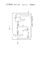
- FIG. 1 is a block diagram of the subject parity circuit
- FIG. 2 is a detailed schematic diagram of the sequential bit evaluator
- FIG. 3 is a timing diagram of waveforms that occur for a five input data transmission to the sequential bit evaluator.
- FIG. 4 illustrates an application of the subject parity circuit for use in a data transmission system as both a parity bit generator and a parity bit checker
- FIG. 5 illustrates a sample DATA SET as it appears to the parity bit generator and parity bit checker shown in FIG. 4.
- FIG. 1 illustrates parity circuit 100 comprising input simultaneous bit evaluator 101, sequential bit evaluator 102 and output simultaneous bit evaluator 103.
- Parity circuit 100 receives a prescribed set of serial bytes of data and generates a single parity bit (P) for the entire data set. The serial bytes of data are transmitted simultaneously on a one byte per lead basis over n data transmission leads (A-E). Parity circuit 100 generates odd parity in the preferred embodiment. Therefore, a single 0 bit is output on lead P if the entire DATA SET has odd parity and a single 1 bit is output on lead P if the entire DATA SET has even parity.
- FIG. 1 illustrates a five input parity circuit 100 which monitors data transmission leads A through E.
- the prescribed DATA SET for a five input data transmission comprises five bytes A through E of digital data. Each byte of digital data includes eight serially transmitted data bits.
- the DATA SET therefore, consists of a 40 bit transmission.
- the 40 bits are evaluated in a sequential manner according to divisions referred to as increments.
- An increment includes all the data bits in a corresponding bit position in the five bytes of data.
- the five data bits which make up each increment are transmitted simultaneously and in synchronization over the five data transmission leads A through E to parity circuit 100.
- Data transmission leads A through E connect to the logic in input simultaneous bit evaluator 101 where four exclusive OR gates 110 through 113 combine the data bits in each increment that appear on the five data transmission leads.
- input simultaneous bit evaluator 101 produces a single bit on lead 114 which is representative of either an even or odd number of 1 bits included in an increment.
- increment 0 of prescribed DATA SET N (FIG. 3) has an arbitrary bit pattern of 1,1,0,0,0.
- the representative bit produced by input simultaneous bit evaluator 101 for this increment is a 0, which represents that there are an even number of 1 bits in the 0 increment.
- Exclusive OR gate 110 combines the data bits received on data transmission leads A and B
- exclusive OR gate 111 combines the data bits received on data transmission leads C and D
- Exclusive OR gate 112 combines the signals output by exclusive OR gates 110 and 111.
- Exclusive OR gate 113 combines the signals output by exclusive OR gate 112 and the data bit received on data transmission lead E resulting in the representative bit which is applied to lead 114.
- sequential bit evaluator 102 The representative bit for each increment of data is applied over lead 114 to sequential bit evaluator 102.
- the logic in sequential bit evaluator 102 is explained in greater detail subsequently.
- sequential bit evaluator 102 sequentially monitors all incoming representative bits 0 through 6 for the DATA SET to determine the even or odd state of each representative bit. With the appearance of the next to the last (6th) representative bit, sequential bit evaluator 102 provides an output called the indicative bit which indicates whether an even or odd number of 1 bits have thus far been included in the data transmission. Sequential bit evaluator 102 applies this indicative bit over lead 124 during the occurrence of the last increment to output simultaneous bit evaluator 103.
- a single parity bit is generated for the entire DATA SET rather than on a per byte basis. Therefore, one byte is selected to transmit the parity bit for the DATA SET.
- the parity bit (P) is inserted into the final bit position of this byte, for example the B byte as shown in FIG. 1.
- Output simultaneous bit evaluator 103 receives the indicative bit from sequential bit evaluator 102 and the last increment (less the last bit on lead B) from data transmission leads A-E.
- Output simultaneous bit evaluator 103 comprises four exclusive OR gates 120 through 123. Sequential bit evaluator 102 applies the indicative bit over lead 124 and the last increment bit in byte A appears on data transmission lead A to exclusive OR gate 121.
- Exclusive OR gate 120 combines the last increment data bits of bytes C and D received on data transmission leads C and D.
- Exclusive OR gate 122 combines the outputs of exclusive OR gates 120 and 121.
- Exclusive OR gate 123 combines the output of exclusive OR gate 122 and the last bit of byte E applied over data transmission lead E, and generates a single parity bit (P).
- the subject parity circuit 100 serves to evaluate the multiple bytes of serial data comprising a data set, and generates a single parity bit (P) for the entire DATA SET.
- parity circuit 100 simultaneously combines and evaluates the increments of data in a prescribed set that are transmitted over a plurality of data transmission leads.
- the following description deals specifically with sequential bit evaluator 102 and the logic operations that occur as the representative bits are evaluated to produce the indicative bit which is pivotal in generating the single parity bit (P) for the entire DATA SET.
- FIG. 3 shows signals that represent the transmission sequence of three DATA SETS.
- DATA SETS N and N+2 will be used.
- Five bytes of eight bits per byte comprise a DATA SET, and the five bits in each bit position comprise an increment.
- the bytes are designated A through E and are transmitted to parity circuit 100 on data transmission leads A through E. These transmissions have the indicated arbitrary bit patterns for each byte.
- Sequential bit evaluator 102 performs initialization operations at the beginning of each DATA SET with the arrival of the 0 representative bit. Thereafter, all the representative bits which are input over lead 114 to sequential bit evaluator 102 are monitored to determine whether an even or odd number of 1 bits are included in the DATA SET prior to the generation of the last representative bit. Sequential bit evaluator 102 generates a bit indicative of an odd or even number of 1 bits in a DATA SET with the occurrence of the next to the last (6th) increment of a DATA SET.
- the clock serves to synchronize the operations of the data processing circuits.
- the system clock circuit applies signals on leads BTO, BTO*, BT7* to define the beginning and end of the DATA SET.
- the action of gates (201--204) in sequential bit evaluator 102 alleviates the need to reset flip-flop 206 at the beginning of each new DATA SET.
- the subject circuit simply establishes the state of flip-flop 206 at representative bit 0 rather than resetting flip-flop 206.
- the state of flip-flop 206 is set such that the Q output of flip-flop 206 agrees with the even or odd state of the 0 representative bit.
- lead BTO* (214) carries a 0 or low and lead BT7* carries a 1 or high.
- Lead BTO* (214) therefore, serves to inhibit AND gate 201 during the 0 representative bit and a 0 or low is applied to lead 208.
- the general system clock transmits a signal on lead BTO which signal is the inverse of the signal appearing on lead BTO*.
- lead BTO (216) always carries a 1 or high to AND gate 203.
- representative bits 1 through 7 lead BTO (216) carries a 0 or low to AND gate 203.
- lead BTO (216) enables AND gate 203 only during representative bit 0.
- the signal on lead 209 is therefore only significant during representative bit 0.
- AND gate 203 transmits a 1 or high over lead 210 to OR gate 204.
- OR gate 204 transmits a 1 or high over lead 211 to the toggle input terminal of flip-flop 206.
- Flip-flop 206 now toggles at the negative edge of the clock pulse applied to lead BCLK by system clock during this 0 representative bit.
- Flip-flop 206 output Q is now a 0 or low and the state of flip-flop 206 now matches the 0 representative bit.
- the signal on lead 211 causes flip-flop 206 to change state as follows.
- the system clock enables gate 201 via clock leads BTO* and BT7* during representative bits 1-7.
- Gate 201 therefore passes the received representative bit from lead 114 to lead 208.
- Lead 210 always applies a 0 or low to gate 204 during representative bits 1 through 6.
- the signal on lead 208 determines the output of OR gate 204 as applied to lead 211.
- Flip-flop 206 toggles only when OR gate 204 applies a 1 or high to lead 211.
- Flip-flop 206 toggles during a negative edge triggered clock (BCLK) pulse (217) which causes the transition to be centered in a bit period.
- BCLK negative edge triggered clock
- flip-flop 206 monitors representative bits 1 through 6 as they pass through gates 201 and 204 and registers every instance when lead 211 inputs a 1 or high as is the case during representative bits 0, 4, 5 and 6 in DATA SET N. At representative bit 7, flip-flop 206 indicates that an odd number of 1 bits or highs (in this case, 13) have been received by input simultaneous bit evaluator 101. Therefore, flip-flop 206 transmits a low or 0 indicative bit over lead 124 (Q) during the last or 7th increment.
- the indicative bit output by flip-flop 206 over lead 124 is an indication of the odd or even number of 1 bits that have been received by input simultaneous bit evaluator 101 in increments 0 through 6.
- a 0 or low indicative bit is applied to lead 124 if the count is even and a 1 or high indicative bit is applied if the count is odd.
- Output simultaneous bit evaluator 103 then simultaneously combines the indicative bit with the 7th increment bits from bytes A, C, D and E received on data transmission leads A, C, D and E.
- sequential bit evaluator 102 has evaluated the first 35 data bits, increments 0 through 6 in the DATA SET.
- All bits 7 except for the B byte bit 7 are now evaluated in combination with the indicative bit to determine the parity of the DATA SET. If the sum of the 39 data bits evaluated is even, the parity bit (P) will be a 1 or odd. If the sum is odd, the parity bit (P) will be 0. The resulting parity bit is output over lead P. In the present case, output simultaneous bit evaluator 103 applies a 0 or low to lead P (FIG. 1) indicating that the received DATA SET contains an odd number of 1 bits or highs (15) and is maintaining an odd parity.
- the subject parity circuit generates a single parity bit (P) for a DATA SET that is separated into equal portions and synchronously input to the parity circuit over a plurality of data transmission leads.
- This single parity bit (P) identifies the parity of the entire DATA SET which precludes the need for generating a parity bit (P) for each byte of serial data applied over a data transmission lead.
- the generation of a single parity bit (P) serves to efficiently and economically evaluate DATA SETS that are, for example, transmitted through a data-handling system.
- the subject parity circuit has a wide variety of applications that is primarily used to detect errors in data transmissions. Errors are detected when a parity bit generated at the originating end of the data transmission is transmitted to the destination where it is compared with a parity bit generated at the receiving end of data transmission. (See “Computer Logic Design” by M. M. Mano, Prentice-Hall, Inc. (1972), pp. 157-159.)
- FIG. 4 illustrates an application of the subject parity circuit 100 as it may be used in a data-handling system. For explanation purposes, only a two-input system will be discussed although it is to be understood that n data transmission leads may be evaluated by the subject parity circuit.
- FIG. 5 illustrates an arbitrary bit pattern of two bytes, A and B. These bytes comprise a 16 bit DATA SET.
- Parity bit generator 400 comprises parity circuit 100 and multiplexor (MUX) 404. Data transmission leads A and B input to parity bit generator 400. Parity circuit 100 simultaneously and sequentially evaluates the data bits in bytes A and B based on the logic previously described. Thereafter, parity circuit 100 generates a single parity bit (P) during the 7th bit position for the 16 bit DATA SET. In this example, the A byte is designated for parity bit (P) insertion. Therefore, only the A byte inputs to MUX 404.
- MUX multiplexor
- the indicative bit on lead P and the 7th bit on lead A are input to MUX 404 simultaneously.
- the parity bit P is then switched by MUX 404 to replace data bit 7 on the A byte.
- the darkened square A7 in example 2 of FIG. 5 indicates the parity of the DATA SET.
- There are an odd number (7) of 1 bits or highs in the DATA SET therefore, to maintain the odd parity for the preferred embodiment, a 0 or low parity bit is generated.
- Parity bit checker 401 comprises parity circuit 100, exclusive OR gate 405 and AND gate 406. Again, parity circuit 100 evaluates the data bits applied over data transmission leads A' and B, and generates a parity bit (P') for the received DATA SET. Only the generated parity bit (P') and the transmitted parity bit (P) are significant to the parity bit checker circuit and therefore, further discussion deals only with these bits. In the case of parity bit checker 401, the generated parity bit (P') inputs directly to exclusive OR gate 405.
- Transmitted parity bit (P) and generated parity bit (P'), both of which correspond to the 7th bit position are simultaneously input to exclusive OR gate 405.
- Exclusive OR gate 405 then compares the generated parity bit (P') on lead P with received parity bit (P) on data transmission lead A'.
- the output of exclusive OR gate 405 is carried by lead 407 to AND gate 406.
- AND gate 406 is enabled by lead BT7 (408) which receives a signal from the system clock and is the inverse of the signal on lead BT7* upon the arrival of increment 7. With the occurrence of increment 7, the output of AND gate 406 over path ER indicates whether an erroneous transmission occurred.
- Error in transmission is indicated if AND gate 406 outputs a 1 or a high which results from nonmatching parity bits, P and P'. Conversely, if AND gate 406 outputs a 0 or a low, there is no transmission error.
- the single output from parity bit checker 401 indicates the status, erroneous or not, of the transmission of the entire DATA SET. This method precludes error detection for each individual byte of data. Evaluating an entire set of data is quickly and efficiently accomplished.
- FIG. 5 further illustrates an example of an error in the DATA SET and the effect of the above-described application of parity circuit 100 as shown in FIG. 4.
- the bytes A and B have been assigned arbitrary bit patterns and byte A has been designated as the byte that will carry the parity bit in the last position, bit 7.
- Bytes A and B are input to parity bit generator 400 where parity circuit 100, based on the logic located within, evaluates the bits and generates a parity bit (P) for the DATA SET (see examples 501 and 502 on FIG. 5).
- MUX 404 isolates and replaces the 7th bit on the A byte with a 0 or low parity bit indicating that an odd number of data bits are present in the transmission.
- a transmission error occurs (due, for example, to a burst of noise) and that the 0 bit position A2 has been replaced with a 1 or high at some point in the transmission.
- Bytes A' and B as altered by noise are input to parity bit checker 401 where parity circuit 100 evaluates the DATA SET and outputs generated parity bit (P') to exclusive OR gate 405.
- generated parity bit P' is a 1 or high which indicates there is an even number (8) of 1 bits or highs in the DATA SET (bytes A' and B).
- exclusive OR gate 405 and AND gate 406 compares received parity bit (bit 7 on byte A') with generated parity bit (P') to determine if an erroneous transmission has occurred. Note, that A' 7 is a 0 and P' is a 1 and, as a result, AND gate 406 outputs over lead ER a 1 or high. Therefore, an error is indicated in the data transmission.
- the above explanation illustrates an application of the subject invention as applied to a data handling system where there are n data transmission leads.
- the subject parity circuit allows for the generation of a single parity bit indicative of the parity of an entire data set.
- the generation of a single parity bit at the transmitting and receiving end of a data transmission system allows the transmissions occurring in defined data sets to be monitored for any erros.
- the design of the subject parity circuit eliminates the need to generate a parity bit for each byte of data appearing on every lead, thus providing a more economical and efficient evaluation of incoming serial data.
Abstract
Description
Claims (10)
Priority Applications (1)
| Application Number | Priority Date | Filing Date | Title |
|---|---|---|---|
| US06/491,279 US4538271A (en) | 1983-05-04 | 1983-05-04 | Single parity bit generation circuit |
Applications Claiming Priority (1)
| Application Number | Priority Date | Filing Date | Title |
|---|---|---|---|
| US06/491,279 US4538271A (en) | 1983-05-04 | 1983-05-04 | Single parity bit generation circuit |
Publications (1)
| Publication Number | Publication Date |
|---|---|
| US4538271A true US4538271A (en) | 1985-08-27 |
Family
ID=23951531
Family Applications (1)
| Application Number | Title | Priority Date | Filing Date |
|---|---|---|---|
| US06/491,279 Expired - Lifetime US4538271A (en) | 1983-05-04 | 1983-05-04 | Single parity bit generation circuit |
Country Status (1)
| Country | Link |
|---|---|
| US (1) | US4538271A (en) |
Cited By (7)
| Publication number | Priority date | Publication date | Assignee | Title |
|---|---|---|---|---|
| US4747106A (en) * | 1984-11-01 | 1988-05-24 | Mitsubishi Denki Kabushiki Kaisha | Parity checker circuit |
| US4757504A (en) * | 1986-04-21 | 1988-07-12 | Texas Instruments Incorporated | Polyphase parity generator circuit |
| US5335235A (en) * | 1992-07-07 | 1994-08-02 | Digital Equipment Corporation | FIFO based parity generator |
| US5517514A (en) * | 1992-11-12 | 1996-05-14 | Amdahl Corporation | Parity checking system with reduced usage of I/O pins |
| US6108763A (en) * | 1986-09-18 | 2000-08-22 | Grondalski; Robert S. | Simultaneous parity generating/reading circuit for massively parallel processing systems |
| US7572237B2 (en) | 2002-11-06 | 2009-08-11 | Abbott Diabetes Care Inc. | Automatic biological analyte testing meter with integrated lancing device and methods of use |
| US20110142074A1 (en) * | 2009-12-16 | 2011-06-16 | William Henry Lueckenbach | Serial communication module with multiple receiver/transmitters |
Citations (1)
| Publication number | Priority date | Publication date | Assignee | Title |
|---|---|---|---|---|
| US3487363A (en) * | 1967-08-31 | 1969-12-30 | Bell Telephone Labor Inc | Asynchronous parity checking circuit |
-
1983
- 1983-05-04 US US06/491,279 patent/US4538271A/en not_active Expired - Lifetime
Patent Citations (1)
| Publication number | Priority date | Publication date | Assignee | Title |
|---|---|---|---|---|
| US3487363A (en) * | 1967-08-31 | 1969-12-30 | Bell Telephone Labor Inc | Asynchronous parity checking circuit |
Non-Patent Citations (6)
| Title |
|---|
| Grimes, IBM Technical Disclosure Bulletin, Two Dimensional Parity Error Correction Procedure, vol. 25, No. 5, 10/82, pp. 2686 2689. * |
| Grimes, IBM Technical Disclosure Bulletin, Two-Dimensional Parity Error Correction Procedure, vol. 25, No. 5, 10/82, pp. 2686-2689. |
| Hill, Introduction to Switching Theory and Logical Design, 2nd ed., 1974, p. 202, 3rd ed., 1981, pp. 241 244. * |
| Hill, Introduction to Switching Theory and Logical Design, 2nd ed., 1974, p. 202, 3rd ed., 1981, pp. 241-244. |
| Mano, Computer Logic Design, 1972, pp. 157 159. * |
| Mano, Computer Logic Design, 1972, pp. 157-159. |
Cited By (10)
| Publication number | Priority date | Publication date | Assignee | Title |
|---|---|---|---|---|
| US4747106A (en) * | 1984-11-01 | 1988-05-24 | Mitsubishi Denki Kabushiki Kaisha | Parity checker circuit |
| US4757504A (en) * | 1986-04-21 | 1988-07-12 | Texas Instruments Incorporated | Polyphase parity generator circuit |
| US6108763A (en) * | 1986-09-18 | 2000-08-22 | Grondalski; Robert S. | Simultaneous parity generating/reading circuit for massively parallel processing systems |
| US5335235A (en) * | 1992-07-07 | 1994-08-02 | Digital Equipment Corporation | FIFO based parity generator |
| US5517514A (en) * | 1992-11-12 | 1996-05-14 | Amdahl Corporation | Parity checking system with reduced usage of I/O pins |
| US7572237B2 (en) | 2002-11-06 | 2009-08-11 | Abbott Diabetes Care Inc. | Automatic biological analyte testing meter with integrated lancing device and methods of use |
| US20090259147A1 (en) * | 2002-11-06 | 2009-10-15 | Abbott Diabetes Care Inc. | Automatic biological analyte testing meter with integrated lancing device and methods of use |
| US8079961B2 (en) | 2002-11-06 | 2011-12-20 | Abbott Diabetes Care Inc. | Automatic biological analyte testing meter with integrated lancing device and methods of use |
| US9060727B2 (en) | 2002-11-06 | 2015-06-23 | Abbott Diabetes Care Inc. | Automatic biological analyte testing meter with integrated lancing device and methods of use |
| US20110142074A1 (en) * | 2009-12-16 | 2011-06-16 | William Henry Lueckenbach | Serial communication module with multiple receiver/transmitters |
Similar Documents
| Publication | Publication Date | Title |
|---|---|---|
| US4920535A (en) | Demultiplexer system | |
| US4498174A (en) | Parallel cyclic redundancy checking circuit | |
| US4635261A (en) | On chip test system for configurable gate arrays | |
| US3648237A (en) | Apparatus and method for obtaining synchronization of a maximum length pseudorandom sequence | |
| EP0425851B1 (en) | Apparatus for decoding frames from a data link | |
| KR100346837B1 (en) | Data recovery apparatus for minimizing error due to the clock skew and method thereof | |
| US3069504A (en) | Multiplex pulse code modulation system | |
| US3567916A (en) | Apparatus for parity checking a binary register | |
| US4538271A (en) | Single parity bit generation circuit | |
| JPS6340080B2 (en) | ||
| US4057834A (en) | Signal compression system for binary digital signals | |
| US4481648A (en) | Method and system for producing a synchronous signal from _cyclic-redundancy-coded digital data blocks | |
| EP0265080A1 (en) | Device for detecting bit phase difference | |
| US4234953A (en) | Error density detector | |
| US3056108A (en) | Error check circuit | |
| JPS6386630A (en) | Frame synchronization system in parallel transmission line | |
| CA1074920A (en) | Detection of errors in digital signals | |
| US6430198B1 (en) | Apparatus and method of reducing packet length count processing | |
| JP3217993B2 (en) | Parity check circuit | |
| CA2020343C (en) | Time-division multiplex communication system with a synchronizing circuit at the receiving end which responds to the coding of words inserted in the transmitted information | |
| JP2814978B2 (en) | Frame synchronization circuit | |
| CA1264830A (en) | Data recovery and clock circuit for use in data test equipment | |
| JPH0614649B2 (en) | Terminal adapter having multiple HDLC communication channel receiver | |
| JPH0450777B2 (en) | ||
| SU1424023A1 (en) | Device for interfacing computer with synchronous data transmission channel |
Legal Events
| Date | Code | Title | Description |
|---|---|---|---|
| AS | Assignment |
Owner name: AMERICAN BELL INC., HOLMDEL, N.J. 07733, A CORP. O Free format text: ASSIGNMENT OF ASSIGNORS INTEREST.;ASSIGNOR:KOHS, DWIGHT W.;REEL/FRAME:004127/0003 Effective date: 19830426 |
|
| STCF | Information on status: patent grant |
Free format text: PATENTED CASE |
|
| FEPP | Fee payment procedure |
Free format text: PAYOR NUMBER ASSIGNED (ORIGINAL EVENT CODE: ASPN); ENTITY STATUS OF PATENT OWNER: LARGE ENTITY |
|
| FPAY | Fee payment |
Year of fee payment: 4 |
|
| FEPP | Fee payment procedure |
Free format text: PAYER NUMBER DE-ASSIGNED (ORIGINAL EVENT CODE: RMPN); ENTITY STATUS OF PATENT OWNER: LARGE ENTITY Free format text: PAYOR NUMBER ASSIGNED (ORIGINAL EVENT CODE: ASPN); ENTITY STATUS OF PATENT OWNER: LARGE ENTITY |
|
| FPAY | Fee payment |
Year of fee payment: 8 |
|
| FEPP | Fee payment procedure |
Free format text: PAYER NUMBER DE-ASSIGNED (ORIGINAL EVENT CODE: RMPN); ENTITY STATUS OF PATENT OWNER: LARGE ENTITY Free format text: PAYOR NUMBER ASSIGNED (ORIGINAL EVENT CODE: ASPN); ENTITY STATUS OF PATENT OWNER: LARGE ENTITY |
|
| FPAY | Fee payment |
Year of fee payment: 12 |