US4498224A - Method of manufacturing a MOSFET using accelerated ions to form an amorphous region - Google Patents
Method of manufacturing a MOSFET using accelerated ions to form an amorphous region Download PDFInfo
- Publication number
- US4498224A US4498224A US06/544,991 US54499182A US4498224A US 4498224 A US4498224 A US 4498224A US 54499182 A US54499182 A US 54499182A US 4498224 A US4498224 A US 4498224A
- Authority
- US
- United States
- Prior art keywords
- manufacturing
- impurities
- region
- insulation layer
- source
- Prior art date
- Legal status (The legal status is an assumption and is not a legal conclusion. Google has not performed a legal analysis and makes no representation as to the accuracy of the status listed.)
- Expired - Lifetime
Links
- 150000002500 ions Chemical class 0.000 title claims abstract description 35
- 238000004519 manufacturing process Methods 0.000 title claims abstract description 18
- 239000000758 substrate Substances 0.000 claims abstract description 33
- 238000009413 insulation Methods 0.000 claims abstract description 31
- 239000012535 impurity Substances 0.000 claims abstract description 29
- 238000000034 method Methods 0.000 claims abstract description 26
- 239000013078 crystal Substances 0.000 claims abstract description 19
- 239000004065 semiconductor Substances 0.000 claims abstract description 10
- 238000010438 heat treatment Methods 0.000 claims abstract description 7
- 238000009792 diffusion process Methods 0.000 claims description 10
- 239000000463 material Substances 0.000 claims description 8
- 229910052594 sapphire Inorganic materials 0.000 claims description 3
- 239000010980 sapphire Substances 0.000 claims description 3
- VYPSYNLAJGMNEJ-UHFFFAOYSA-N Silicium dioxide Chemical compound O=[Si]=O VYPSYNLAJGMNEJ-UHFFFAOYSA-N 0.000 description 10
- 229910052681 coesite Inorganic materials 0.000 description 5
- 229910052906 cristobalite Inorganic materials 0.000 description 5
- 229910021420 polycrystalline silicon Inorganic materials 0.000 description 5
- 239000000377 silicon dioxide Substances 0.000 description 5
- 229910052682 stishovite Inorganic materials 0.000 description 5
- 229910052905 tridymite Inorganic materials 0.000 description 5
- 238000010276 construction Methods 0.000 description 4
- 229920002120 photoresistant polymer Polymers 0.000 description 4
- 238000006243 chemical reaction Methods 0.000 description 3
- 230000003247 decreasing effect Effects 0.000 description 3
- 230000005496 eutectics Effects 0.000 description 3
- 229910052710 silicon Inorganic materials 0.000 description 3
- IJGRMHOSHXDMSA-UHFFFAOYSA-N Atomic nitrogen Chemical compound N#N IJGRMHOSHXDMSA-UHFFFAOYSA-N 0.000 description 2
- 230000001133 acceleration Effects 0.000 description 2
- 230000007547 defect Effects 0.000 description 2
- 230000003647 oxidation Effects 0.000 description 2
- 238000007254 oxidation reaction Methods 0.000 description 2
- 229910021417 amorphous silicon Inorganic materials 0.000 description 1
- QVGXLLKOCUKJST-UHFFFAOYSA-N atomic oxygen Chemical compound [O] QVGXLLKOCUKJST-UHFFFAOYSA-N 0.000 description 1
- 229910052796 boron Inorganic materials 0.000 description 1
- -1 boron ions Chemical class 0.000 description 1
- 230000015556 catabolic process Effects 0.000 description 1
- 238000005229 chemical vapour deposition Methods 0.000 description 1
- 230000000295 complement effect Effects 0.000 description 1
- 238000006731 degradation reaction Methods 0.000 description 1
- 238000000151 deposition Methods 0.000 description 1
- 230000008021 deposition Effects 0.000 description 1
- 230000000694 effects Effects 0.000 description 1
- 230000002349 favourable effect Effects 0.000 description 1
- 238000012986 modification Methods 0.000 description 1
- 230000004048 modification Effects 0.000 description 1
- 229910052757 nitrogen Inorganic materials 0.000 description 1
- 239000001301 oxygen Substances 0.000 description 1
- 229910052760 oxygen Inorganic materials 0.000 description 1
- 230000000149 penetrating effect Effects 0.000 description 1
- 239000000126 substance Substances 0.000 description 1
Images


Classifications
-
- H—ELECTRICITY
- H01—ELECTRIC ELEMENTS
- H01L—SEMICONDUCTOR DEVICES NOT COVERED BY CLASS H10
- H01L21/00—Processes or apparatus adapted for the manufacture or treatment of semiconductor or solid state devices or of parts thereof
- H01L21/02—Manufacture or treatment of semiconductor devices or of parts thereof
- H01L21/04—Manufacture or treatment of semiconductor devices or of parts thereof the devices having at least one potential-jump barrier or surface barrier, e.g. PN junction, depletion layer or carrier concentration layer
- H01L21/18—Manufacture or treatment of semiconductor devices or of parts thereof the devices having at least one potential-jump barrier or surface barrier, e.g. PN junction, depletion layer or carrier concentration layer the devices having semiconductor bodies comprising elements of Group IV of the Periodic System or AIIIBV compounds with or without impurities, e.g. doping materials
- H01L21/26—Bombardment with radiation
- H01L21/263—Bombardment with radiation with high-energy radiation
- H01L21/265—Bombardment with radiation with high-energy radiation producing ion implantation
- H01L21/26506—Bombardment with radiation with high-energy radiation producing ion implantation in group IV semiconductors
- H01L21/26513—Bombardment with radiation with high-energy radiation producing ion implantation in group IV semiconductors of electrically active species
-
- H—ELECTRICITY
- H01—ELECTRIC ELEMENTS
- H01L—SEMICONDUCTOR DEVICES NOT COVERED BY CLASS H10
- H01L21/00—Processes or apparatus adapted for the manufacture or treatment of semiconductor or solid state devices or of parts thereof
- H01L21/02—Manufacture or treatment of semiconductor devices or of parts thereof
- H01L21/04—Manufacture or treatment of semiconductor devices or of parts thereof the devices having at least one potential-jump barrier or surface barrier, e.g. PN junction, depletion layer or carrier concentration layer
- H01L21/18—Manufacture or treatment of semiconductor devices or of parts thereof the devices having at least one potential-jump barrier or surface barrier, e.g. PN junction, depletion layer or carrier concentration layer the devices having semiconductor bodies comprising elements of Group IV of the Periodic System or AIIIBV compounds with or without impurities, e.g. doping materials
- H01L21/22—Diffusion of impurity materials, e.g. doping materials, electrode materials, into or out of a semiconductor body, or between semiconductor regions; Interactions between two or more impurities; Redistribution of impurities
- H01L21/225—Diffusion of impurity materials, e.g. doping materials, electrode materials, into or out of a semiconductor body, or between semiconductor regions; Interactions between two or more impurities; Redistribution of impurities using diffusion into or out of a solid from or into a solid phase, e.g. a doped oxide layer
- H01L21/2251—Diffusion into or out of group IV semiconductors
- H01L21/2252—Diffusion into or out of group IV semiconductors using predeposition of impurities into the semiconductor surface, e.g. from a gaseous phase
- H01L21/2253—Diffusion into or out of group IV semiconductors using predeposition of impurities into the semiconductor surface, e.g. from a gaseous phase by ion implantation
-
- H—ELECTRICITY
- H01—ELECTRIC ELEMENTS
- H01L—SEMICONDUCTOR DEVICES NOT COVERED BY CLASS H10
- H01L21/00—Processes or apparatus adapted for the manufacture or treatment of semiconductor or solid state devices or of parts thereof
- H01L21/02—Manufacture or treatment of semiconductor devices or of parts thereof
- H01L21/04—Manufacture or treatment of semiconductor devices or of parts thereof the devices having at least one potential-jump barrier or surface barrier, e.g. PN junction, depletion layer or carrier concentration layer
- H01L21/18—Manufacture or treatment of semiconductor devices or of parts thereof the devices having at least one potential-jump barrier or surface barrier, e.g. PN junction, depletion layer or carrier concentration layer the devices having semiconductor bodies comprising elements of Group IV of the Periodic System or AIIIBV compounds with or without impurities, e.g. doping materials
- H01L21/26—Bombardment with radiation
- H01L21/263—Bombardment with radiation with high-energy radiation
- H01L21/265—Bombardment with radiation with high-energy radiation producing ion implantation
- H01L21/26506—Bombardment with radiation with high-energy radiation producing ion implantation in group IV semiconductors
-
- H—ELECTRICITY
- H01—ELECTRIC ELEMENTS
- H01L—SEMICONDUCTOR DEVICES NOT COVERED BY CLASS H10
- H01L29/00—Semiconductor devices adapted for rectifying, amplifying, oscillating or switching, or capacitors or resistors with at least one potential-jump barrier or surface barrier, e.g. PN junction depletion layer or carrier concentration layer; Details of semiconductor bodies or of electrodes thereof ; Multistep manufacturing processes therefor
- H01L29/02—Semiconductor bodies ; Multistep manufacturing processes therefor
- H01L29/06—Semiconductor bodies ; Multistep manufacturing processes therefor characterised by their shape; characterised by the shapes, relative sizes, or dispositions of the semiconductor regions ; characterised by the concentration or distribution of impurities within semiconductor regions
- H01L29/08—Semiconductor bodies ; Multistep manufacturing processes therefor characterised by their shape; characterised by the shapes, relative sizes, or dispositions of the semiconductor regions ; characterised by the concentration or distribution of impurities within semiconductor regions with semiconductor regions connected to an electrode carrying current to be rectified, amplified or switched and such electrode being part of a semiconductor device which comprises three or more electrodes
- H01L29/0843—Source or drain regions of field-effect devices
- H01L29/0847—Source or drain regions of field-effect devices of field-effect transistors with insulated gate
-
- H—ELECTRICITY
- H01—ELECTRIC ELEMENTS
- H01L—SEMICONDUCTOR DEVICES NOT COVERED BY CLASS H10
- H01L29/00—Semiconductor devices adapted for rectifying, amplifying, oscillating or switching, or capacitors or resistors with at least one potential-jump barrier or surface barrier, e.g. PN junction depletion layer or carrier concentration layer; Details of semiconductor bodies or of electrodes thereof ; Multistep manufacturing processes therefor
- H01L29/66—Types of semiconductor device ; Multistep manufacturing processes therefor
- H01L29/68—Types of semiconductor device ; Multistep manufacturing processes therefor controllable by only the electric current supplied, or only the electric potential applied, to an electrode which does not carry the current to be rectified, amplified or switched
- H01L29/76—Unipolar devices, e.g. field effect transistors
- H01L29/772—Field effect transistors
- H01L29/78—Field effect transistors with field effect produced by an insulated gate
- H01L29/786—Thin film transistors, i.e. transistors with a channel being at least partly a thin film
- H01L29/78606—Thin film transistors, i.e. transistors with a channel being at least partly a thin film with supplementary region or layer in the thin film or in the insulated bulk substrate supporting it for controlling or increasing the safety of the device
- H01L29/78618—Thin film transistors, i.e. transistors with a channel being at least partly a thin film with supplementary region or layer in the thin film or in the insulated bulk substrate supporting it for controlling or increasing the safety of the device characterised by the drain or the source properties, e.g. the doping structure, the composition, the sectional shape or the contact structure
- H01L29/78621—Thin film transistors, i.e. transistors with a channel being at least partly a thin film with supplementary region or layer in the thin film or in the insulated bulk substrate supporting it for controlling or increasing the safety of the device characterised by the drain or the source properties, e.g. the doping structure, the composition, the sectional shape or the contact structure with LDD structure or an extension or an offset region or characterised by the doping profile
-
- Y—GENERAL TAGGING OF NEW TECHNOLOGICAL DEVELOPMENTS; GENERAL TAGGING OF CROSS-SECTIONAL TECHNOLOGIES SPANNING OVER SEVERAL SECTIONS OF THE IPC; TECHNICAL SUBJECTS COVERED BY FORMER USPC CROSS-REFERENCE ART COLLECTIONS [XRACs] AND DIGESTS
- Y10—TECHNICAL SUBJECTS COVERED BY FORMER USPC
- Y10S—TECHNICAL SUBJECTS COVERED BY FORMER USPC CROSS-REFERENCE ART COLLECTIONS [XRACs] AND DIGESTS
- Y10S148/00—Metal treatment
- Y10S148/082—Ion implantation FETs/COMs
Definitions
- This invention relates to a manufacturing method for a MOSFET type integrated circuit having a relatively short channel, whose source and drain electrodes are connected electrically to source and drain regions in a semiconductor substrate.
- FIG. 1 A structure of a prior art MOSFET is shown in FIG. 1.
- the structure is formed using the following process: First, a thick insulation layer (2) made of SiO 2 is selectively formed on a P type semiconductor substrate (1) made of Si. A thin insulation layer and a polycrystalline silicon (Poly-Si) layer are formed on the exposed surface of the substrate (1). The thin insulation layer and the polycrystalline silicon layer are removed selectively through a photo engraving process, and become gate insulation layer (3) and gate electrode (4), respectively. N type impurities are implanted in substrate (1) using a mask on the gate insulation layer (3) and the gate electrode (4). The implanted N type impurities are activated in a heating step and source and drain regions (5) and (6) are thus formed.
- a thick insulation layer (2) made of SiO 2 is selectively formed on a P type semiconductor substrate (1) made of Si.
- a thin insulation layer and a polycrystalline silicon (Poly-Si) layer are formed on the exposed surface of the substrate (1).
- an insulation layer (7) made of SiO 2 is deposited on the entire surface and contact holes (8) and (9) are formed by a photo engraving process.
- a layer of Al is deposited on the whole surface including the contact holes (8) and (9).
- the Al layer is patterned by a photo engraving process, selectively removed, and source and drain electrodes (10) and (11) are thus formed.
- the source and drain regions (5) and (6) must have a high concentration of impurities in order to obtain favorable ohmic contact with the Al electrodes. And it is desirable that the source and drain regions (5) and (6) are formed deeper.
- Al electrodes (10) and (11) can penetrate as a spike into the source and drain regions (5) and (6) by a eutectic reaction of Al and Si, make contact with the P type substrate (1), and destroy the function of MOSFET.
- the deeper source and drain regions (5) and (6) are formed using conventional processes, the more the diffusion of impurities in the lateral direction is increased.
- This increased lateral diffusion has the disadvantage of unnecessarily decreasing the effective channel length and prevents a fine structure from being achieved because the gate electrode must be formed larger to prevent this occurrence.
- This increased lateral diffusion also can cause the fluctuation of the threshold voltage because it is very difficult to control the extent of the diffusion in the lateral direction.
- the depletion layer of the drain region may reach the source region in a operating state, a "punch-through" phenomenon, and the MOSFET device may not operate with a predetermined characteristic.
- Source and drain regions (5) and (6) can be formed shallower than those of FIG. 1 using prior art processes.
- source and drain electrodes (10) and (11) still can reach the substrate (1) because they penetrate as a spike into the source and drain regions (5) and (6) as a result of the eutectic reaction of Al and Si.
- the sheet resistivity of the source and drain regions becomes high because these regions are formed shallower and cannot be formed with high concentration of impurities.
- source and drain electrodes (10) and (11) can be formed with a gap in mask alignment, and this problem is depicted in FIG. 3.
- contact hole (9) may not be formed solely on the drain region (6) but may be formed on the intersection of the drain region (6) and substrate (1).
- drain electrode (11) can become shorted to substrate (1), and the MOSFET can lose its intended function.
- Another object of this invention is to provide an improved method for manufacturing MOSFETS wherein the portion of the source or drain region in contact with the electrode is deeper than other portions of the source or drain region.
- Another object of this invention is to provide an improved method for manufacturing MOSFETS that is suitable for forming "short channel" MOSFET devices.
- the improved method for manufacturing a MOSFET comprises the steps of
- FIGS. 1 to 3 are sectional views of prior art MOSFET devices made using conventional processes
- FIGS. 4 to 8 are sectional views of a MOSFET at various stages of construction according to a preferred embodiment of this invention.
- FIGS. 9 and 10 are sectional view of a MOSFET at various stages of construction according to another embodiment of the invention.
- FIGS. 4 to 8 designate identical or corresponding parts throughout the several views, and more particularly to FIGS. 4 to 8 thereof, wherein one embodiment of the method of manufacturing a MOSFET according to this invention is illustrated.
- the manufacturing method according to this invention utilizes the phenomenon that the diffusion velocity of an impurity in an amorphous material is faster than that of the impurity in a single crystal of the same material.
- An insulation layer is applied to cover the region on which the first accelerated ions to convert the conductive type are deposited.
- second accelerated ions are introduced into the substrate through contact holes formed in the insulation layer to overlap the first accelerated ion layer, to disorganize the crystal lattice in the overlapped portion whereby the substrate is converted from a single crystal to an amorphous state.
- the first accelerated ions are activated and diffused in the substrate using a heating step.
- the resulting PN junction formed in the amorphous material is deeper than that in the single crystal because the impurities are diffused faster in the amorphous material than in the single crystal.
- PN junction in the semiconductor region under the contact hole is deeper than the PN junction formed in the semiconductor region close to the source-drain channel.
- an Al layer is deposited in the contact holes to form source and drain electrodes.
- the electrodes are favorably contacted with portions of the source and drain regions having deep PN junctions, and the lateral diffusion to the channel region is very small because the source and drain regions close to the channel region are relatively shallow compared to the PN junctions in the electrode regions.
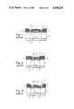
- FIGS. 4 to 8 A preferred embodiment is shown in FIGS. 4 to 8 and the following steps are used.
- a thick insulation layer made of SiO 2 is formed on a P type Si substrate (12) by a thermal oxidation technique. This insulation layer is selectively removed to form field insulation layer (13) as shown in FIG. 4.
- substrate (12) is heated again and a thin insulation layer is formed on the exposed surface of the substrate (12), and a poly-Si layer including As as an impurity is deposited on the thin insulation layer in succession.
- the thickness of the thin insulation layer is about 500 A.
- the poly-Si layer is then patterned and selectively removed to form gate electrode (14).
- the thin insulation layer is also patterned by using the gate electrode (14) as a mask to form gate insulation layer (15).
- accelerated impurity ions for example As ions
- As ions are deposited on the exposed surface of the substrate (12), and As ion layers (16) and (17) are formed as shown in FIG. 5.
- a very thin insulation layer (not shown) may be formed on the exposed surface of the substrate (12). In the latter case, the accelerated ions will be deposited through the very thin insulation layer.
- As ions are introduced with an acceleration voltage of 40 keV and a dose volume of 2 ⁇ 10 15 /cm 2 .
- insulation layer (18) made of SiO 2 is coated on the entire surface by chemical vapor deposition and photoresist layer (19) is coated thereon.
- Photoresist layer (19) is selectively removed through a photo engraving process to provide a pattern for forming contact holes. Insulation layer (18) is then selectively removed by using photoresist layer (19) as a mask and contact holes (20) and (21) are thereby formed.
- accelerated Si ions are introduced into the substrate (12) through contact holes (20) and (21) with an acceleration voltage of 100 keV and a dose volume of 1 ⁇ 10 15 /cm 2 .
- the portions of the crystal of the substrate (12) in which Si ions were introduced are converted from a crystalline state to an amorphous state through this step and amorphous layers (22) and (23) are formed in the substrate (12) as shown in FIG. 6.
- the photoresist layer (19) is removed, and the substrate (12) is heated at a temperature of about 700° C., whereupon a solidus growth advances from the single crystal layer, which acts as a seed crystal, into the amorphous regions, and the amorphous layers (22) and (23) are converted back to single crystal layers.
- the N type impurities, As ions in this case are activated and diffused into the substrate (12).
- the PN junction in source and drain regions (24) and (25) becomes deep in the regions under the contact holes and remains shallow in other regions including the regions close to the channel region between source and drain regions (24) and (25) as shown in FIG. 7.
- the resistance value is high in the region in which the accelerated ions are not fully activated, it is more important to restrain the diffusion in the lateral direction toward the channel region.
- the increase resistance value is not as important in this case because of the significant decrease in the resistance in the regions of contact with electrodes.
- an Al layer is evaporated on insulation layer (18) and into contact holes (20) and (21).
- the Al layer is then patterned by a photo engraving process and selectively removed, forming source and drain electrodes (26) and (27) as shown in FIG. 8. Because source and drain electrodes (26) and (27) are in contact with the deep regions of the source and drain regions, low ohmic losses result.
- Al electrodes (26) and (27) are prevented from penetrating as a spike into the source and drain regions (24) and (25) and contacting the substrate (12) with the eutectic reaction of Al and Si. Because the total sheet resistance value in the source and drain regions is decrease, the MOSFET manufactured in accordance with the method of present invention can be operated at a high speed.
- the implanted ions can be activated at a relatively low temperature, so that the MOSFET can be manufactured with a low temperature process and the possibility of thermal degradation of the device can be reduced.
- contact holes (20) and (21) are formed from the As ion layers (16) and (17) using a precise mask alignment step, the amorphous layers (22) and (23), in which the impurities can diffuse at a faster rate, can also be formed directly under the contact holes (20) and (21). Thereafter, the impurities can be diffused quickly into amorphous layers (22) and (23) that are directly under the holes (20) and (21), and the possibility of a short between Al electrodes (26) and (27) and substrate (12) can be prevented.
- FIGS. 9 and 10 A MOSFET made according to another embodiment of the present process invention is shown in FIGS. 9 and 10.
- First epitaxial Si layer (28) is formed on sapphire substrate (29). Then, Si layer (28) is selectively oxidized by local oxidation step to form an SiO 2 field insulation layer (30).
- SiO 2 field insulation layer (30) In order to control the threshold voltage of the MOSFET, accelerated boron ions are deposited in the region in which the channel regions of the MOSFET will be formed.
- Gate insulation layer (31) and gate electrode (32) are formed using the same process substeps as in the embodiment shown in FIGS. 4-8.
- Accelerated As ions are deposited on exposed Si layer (28) by using gate electrode (32), gate insulation layer (31), and field insulation layer (30) as a mask, and As ion layers (33) and (34) are then formed. Insulation layer (37) is then formed to cover Si layer (28), contact holes (35) and (36) are formed in layer (37), and accelerated Si ions are introduced into Si layer (28) through contact holes (35) and (36), again as in the previous embodiment.
- the accelerated Si ions convert impacted portions of Si layer (28) from a crystalline state to an amorphous state, and amorphous Si layers (38) and (39) are formed as shown in FIG. 9.
- the partially completed MOSFET is heated at about 700° C. to form source and drain regions (40) and (41), respectively.
- Source and drain regions (40) and (41) are shallow close to the channel regions and are deep in the regions under contact holes (35) and (36). Following the heating step, source and drain electrodes (42) and (43) made of Al are formed to contact the deep regions of source and drain regions (40) and (41) as shown in FIG. 10.
- the MOSFET made according to the above-mentioned process has the same advantages as the first embodiment, and has the following additional benefits.
- Si layer (28) on the sapphire substrate (29) has many lattice defects which can shorten the lifetime of the carrier and increase the leak current of the device.
- the amorphous layers (38) and (39) are recrystallized in the heating step, and the resulting new crystal has fewer lattice defects, thereby decreasing the MOSFET leak current.
- Si ions are used in the previously described embodiments to disorganize the crystal material to produce an amorphous state
- ions of oxygen, nitrogen and so on can be used. It is preferable to use the same material as the substrate because the chemical stability of the substrate will be maintained.
- N type impurities for example As, may be introduced through the same contact holes.
Abstract
A method for manufacturing MOSFET type semiconductor devices comprises forming a gate insulation layer and a gate electrode on a single crystal semiconductor substrate; introducing impurities in the substrate using the gate electrode as a mask; introducing accelerated ions deeper into the substrate than the impurities and overlapping at least a portion of the region in which the impurities are introduced in order to convert that portion to an amorphous state; diffusing the impurities into the amorphous region using a heating atmosphere, in order to form source and drain regions and, at the same time, converting the amorphous region to a single crystal; and forming source and drain electrodes in contact with the source and drain regions.
Description
This invention relates to a manufacturing method for a MOSFET type integrated circuit having a relatively short channel, whose source and drain electrodes are connected electrically to source and drain regions in a semiconductor substrate.
A structure of a prior art MOSFET is shown in FIG. 1. The structure is formed using the following process: First, a thick insulation layer (2) made of SiO2 is selectively formed on a P type semiconductor substrate (1) made of Si. A thin insulation layer and a polycrystalline silicon (Poly-Si) layer are formed on the exposed surface of the substrate (1). The thin insulation layer and the polycrystalline silicon layer are removed selectively through a photo engraving process, and become gate insulation layer (3) and gate electrode (4), respectively. N type impurities are implanted in substrate (1) using a mask on the gate insulation layer (3) and the gate electrode (4). The implanted N type impurities are activated in a heating step and source and drain regions (5) and (6) are thus formed. Next, an insulation layer (7) made of SiO2 is deposited on the entire surface and contact holes (8) and (9) are formed by a photo engraving process. A layer of Al is deposited on the whole surface including the contact holes (8) and (9). The Al layer is patterned by a photo engraving process, selectively removed, and source and drain electrodes (10) and (11) are thus formed. In this process, the source and drain regions (5) and (6) must have a high concentration of impurities in order to obtain favorable ohmic contact with the Al electrodes. And it is desirable that the source and drain regions (5) and (6) are formed deeper. However, Al electrodes (10) and (11) can penetrate as a spike into the source and drain regions (5) and (6) by a eutectic reaction of Al and Si, make contact with the P type substrate (1), and destroy the function of MOSFET. And, the deeper source and drain regions (5) and (6) are formed using conventional processes, the more the diffusion of impurities in the lateral direction is increased. This increased lateral diffusion has the disadvantage of unnecessarily decreasing the effective channel length and prevents a fine structure from being achieved because the gate electrode must be formed larger to prevent this occurrence. This increased lateral diffusion also can cause the fluctuation of the threshold voltage because it is very difficult to control the extent of the diffusion in the lateral direction. Furthermore, the depletion layer of the drain region may reach the source region in a operating state, a "punch-through" phenomenon, and the MOSFET device may not operate with a predetermined characteristic.
Source and drain regions (5) and (6) can be formed shallower than those of FIG. 1 using prior art processes. In the resulting MOSFET device which is depicted schematically in FIG. 2, source and drain electrodes (10) and (11) still can reach the substrate (1) because they penetrate as a spike into the source and drain regions (5) and (6) as a result of the eutectic reaction of Al and Si. However, the sheet resistivity of the source and drain regions becomes high because these regions are formed shallower and cannot be formed with high concentration of impurities. Furthermore, when source and drain regions (5) and (6) are formed in a fine pattern using conventional processes, source and drain electrodes (10) and (11) can be formed with a gap in mask alignment, and this problem is depicted in FIG. 3. In this situation contact hole (9) may not be formed solely on the drain region (6) but may be formed on the intersection of the drain region (6) and substrate (1). As a result, drain electrode (11) can become shorted to substrate (1), and the MOSFET can lose its intended function.
It is accordingly an object of this invention to provide an improved method for manufacturing MOSFETS whose source and drain electrodes can be formed in a predetermined location relative to the source and drain regions.
Another object of this invention is to provide an improved method for manufacturing MOSFETS wherein the portion of the source or drain region in contact with the electrode is deeper than other portions of the source or drain region.
Another object of this invention is to provide an improved method for manufacturing MOSFETS that is suitable for forming "short channel" MOSFET devices.
In accordance with this invention, the improved method for manufacturing a MOSFET comprises the steps of
forming a gate insulation layer and a gate electrode on a preselected portion of a semiconductive body of single crystal having a first conductivity type,
introducing impurities into the semiconductive body using the gate electrode as a mask,
introducing accelerated ions into the semiconductor body to overlap at least portion of the region in which the impurities are introduced, wherein the accelerated ions are partly introduced deeper than the impurities, to convert that portion of the crystal of the semiconductive body into an amorphous state,
forming a diffused region having a second conductivity type,
and
forming an electrode on the diffused region.
A more complete appreciation of the invention and many of the attendant advantages thereof will be readily obtained as the same become better understood by reference to the following detailed description when considered in connection with the accompanying drawings, wherein
FIGS. 1 to 3 are sectional views of prior art MOSFET devices made using conventional processes;
FIGS. 4 to 8 are sectional views of a MOSFET at various stages of construction according to a preferred embodiment of this invention; and
FIGS. 9 and 10 are sectional view of a MOSFET at various stages of construction according to another embodiment of the invention.
Referring now to the drawings, wherein like reference numerals designate identical or corresponding parts throughout the several views, and more particularly to FIGS. 4 to 8 thereof, wherein one embodiment of the method of manufacturing a MOSFET according to this invention is illustrated.
The manufacturing method according to this invention utilizes the phenomenon that the diffusion velocity of an impurity in an amorphous material is faster than that of the impurity in a single crystal of the same material. An insulation layer is applied to cover the region on which the first accelerated ions to convert the conductive type are deposited. Next, second accelerated ions are introduced into the substrate through contact holes formed in the insulation layer to overlap the first accelerated ion layer, to disorganize the crystal lattice in the overlapped portion whereby the substrate is converted from a single crystal to an amorphous state. After that, the first accelerated ions are activated and diffused in the substrate using a heating step. The resulting PN junction formed in the amorphous material is deeper than that in the single crystal because the impurities are diffused faster in the amorphous material than in the single crystal. In other words, PN junction in the semiconductor region under the contact hole is deeper than the PN junction formed in the semiconductor region close to the source-drain channel. Next, an Al layer is deposited in the contact holes to form source and drain electrodes. The electrodes are favorably contacted with portions of the source and drain regions having deep PN junctions, and the lateral diffusion to the channel region is very small because the source and drain regions close to the channel region are relatively shallow compared to the PN junctions in the electrode regions.
A preferred embodiment is shown in FIGS. 4 to 8 and the following steps are used. First, a thick insulation layer made of SiO2 is formed on a P type Si substrate (12) by a thermal oxidation technique. This insulation layer is selectively removed to form field insulation layer (13) as shown in FIG. 4. Next, substrate (12) is heated again and a thin insulation layer is formed on the exposed surface of the substrate (12), and a poly-Si layer including As as an impurity is deposited on the thin insulation layer in succession. The thickness of the thin insulation layer is about 500 A. The poly-Si layer is then patterned and selectively removed to form gate electrode (14). The thin insulation layer is also patterned by using the gate electrode (14) as a mask to form gate insulation layer (15).
After that, accelerated impurity ions, for example As ions, are deposited on the exposed surface of the substrate (12), and As ion layers (16) and (17) are formed as shown in FIG. 5. Before this step, a very thin insulation layer (not shown) may be formed on the exposed surface of the substrate (12). In the latter case, the accelerated ions will be deposited through the very thin insulation layer. In the embodiment shown in FIG. 5, As ions are introduced with an acceleration voltage of 40 keV and a dose volume of 2×10¹⁵ /cm2.
Following the impurity deposition step, insulation layer (18) made of SiO2 is coated on the entire surface by chemical vapor deposition and photoresist layer (19) is coated thereon. Photoresist layer (19) is selectively removed through a photo engraving process to provide a pattern for forming contact holes. Insulation layer (18) is then selectively removed by using photoresist layer (19) as a mask and contact holes (20) and (21) are thereby formed. Next, accelerated Si ions are introduced into the substrate (12) through contact holes (20) and (21) with an acceleration voltage of 100 keV and a dose volume of 1×10¹⁵ /cm2. The portions of the crystal of the substrate (12) in which Si ions were introduced are converted from a crystalline state to an amorphous state through this step and amorphous layers (22) and (23) are formed in the substrate (12) as shown in FIG. 6. Following the step of forming the amorphous layers, the photoresist layer (19) is removed, and the substrate (12) is heated at a temperature of about 700° C., whereupon a solidus growth advances from the single crystal layer, which acts as a seed crystal, into the amorphous regions, and the amorphous layers (22) and (23) are converted back to single crystal layers. At the same time, the N type impurities, As ions in this case, are activated and diffused into the substrate (12). The rate of difussion into the single crystal is slow, but the diffusion rate into the amorphous regions is much faster than that into the crystalline regions. Therefore, the PN junction in source and drain regions (24) and (25) becomes deep in the regions under the contact holes and remains shallow in other regions including the regions close to the channel region between source and drain regions (24) and (25) as shown in FIG. 7. At the temperature of about 700° C., essentially all of the As ions in the amorphous crystal are activated, but only a part of the As ions in the crystalline regions will be activated. Although the resistance value is high in the region in which the accelerated ions are not fully activated, it is more important to restrain the diffusion in the lateral direction toward the channel region. Moreover, the increase resistance value is not as important in this case because of the significant decrease in the resistance in the regions of contact with electrodes.
Following the heating step, an Al layer is evaporated on insulation layer (18) and into contact holes (20) and (21). The Al layer is then patterned by a photo engraving process and selectively removed, forming source and drain electrodes (26) and (27) as shown in FIG. 8. Because source and drain electrodes (26) and (27) are in contact with the deep regions of the source and drain regions, low ohmic losses result. According to the invention Al electrodes (26) and (27) are prevented from penetrating as a spike into the source and drain regions (24) and (25) and contacting the substrate (12) with the eutectic reaction of Al and Si. Because the total sheet resistance value in the source and drain regions is decrease, the MOSFET manufactured in accordance with the method of present invention can be operated at a high speed.
Undesirable effects which could otherwise appear in MOSFET's having a short channel construction, such as the fluctuation of the threshold voltage and the "punch through" phenomenon mention previously, can be prevented because the PN junction close to the channel region is shallow and unwanted lateral diffusion is decreased. Furthermore, according to this manufacturing process, the implanted ions can be activated at a relatively low temperature, so that the MOSFET can be manufactured with a low temperature process and the possibility of thermal degradation of the device can be reduced. Because contact holes (20) and (21) are formed from the As ion layers (16) and (17) using a precise mask alignment step, the amorphous layers (22) and (23), in which the impurities can diffuse at a faster rate, can also be formed directly under the contact holes (20) and (21). Thereafter, the impurities can be diffused quickly into amorphous layers (22) and (23) that are directly under the holes (20) and (21), and the possibility of a short between Al electrodes (26) and (27) and substrate (12) can be prevented.
A MOSFET made according to another embodiment of the present process invention is shown in FIGS. 9 and 10. First epitaxial Si layer (28) is formed on sapphire substrate (29). Then, Si layer (28) is selectively oxidized by local oxidation step to form an SiO2 field insulation layer (30). In order to control the threshold voltage of the MOSFET, accelerated boron ions are deposited in the region in which the channel regions of the MOSFET will be formed. Gate insulation layer (31) and gate electrode (32) are formed using the same process substeps as in the embodiment shown in FIGS. 4-8. Accelerated As ions are deposited on exposed Si layer (28) by using gate electrode (32), gate insulation layer (31), and field insulation layer (30) as a mask, and As ion layers (33) and (34) are then formed. Insulation layer (37) is then formed to cover Si layer (28), contact holes (35) and (36) are formed in layer (37), and accelerated Si ions are introduced into Si layer (28) through contact holes (35) and (36), again as in the previous embodiment. The accelerated Si ions convert impacted portions of Si layer (28) from a crystalline state to an amorphous state, and amorphous Si layers (38) and (39) are formed as shown in FIG. 9. Next the partially completed MOSFET is heated at about 700° C. to form source and drain regions (40) and (41), respectively. Source and drain regions (40) and (41) are shallow close to the channel regions and are deep in the regions under contact holes (35) and (36). Following the heating step, source and drain electrodes (42) and (43) made of Al are formed to contact the deep regions of source and drain regions (40) and (41) as shown in FIG. 10.
The MOSFET made according to the above-mentioned process has the same advantages as the first embodiment, and has the following additional benefits. Generally, Si layer (28) on the sapphire substrate (29) has many lattice defects which can shorten the lifetime of the carrier and increase the leak current of the device. But, in the present process the amorphous layers (38) and (39) are recrystallized in the heating step, and the resulting new crystal has fewer lattice defects, thereby decreasing the MOSFET leak current.
Although Si ions are used in the previously described embodiments to disorganize the crystal material to produce an amorphous state, ions of oxygen, nitrogen and so on can be used. It is preferable to use the same material as the substrate because the chemical stability of the substrate will be maintained. In addition, after the accelerated Si ions are deposited on Si layer (28) or Si substrate (12) through the contact holes, N type impurities, for example As, may be introduced through the same contact holes. By this additional process step, the possibility of a short circuit between the Al electrode and the substrate is virtually eliminated. Finally, the processes of this invention are also applicable to the construction of P channel type MOSFET's and complementary MOSFET's.
Obviously, many modifications and variations of this invention are possible in the light of the above teachings. It is therefore to be understood that within the scope of the appended claims, this invention may be practiced otherwise than as specifically described.
Claims (8)
1. A method for manufacturing semiconductors of the MOSFET type comprising the steps of:
forming a gate insulation layer and a gate electrode on a selected portion of a semiconductor body of single crystal material having a first conductivity type;
introducing impurities of a second conductivity type into a preselected region of the semiconductor body using the gate electrode as a mask;
introducing accelerated ions to overlap at least a portion of the region in which the impurities are introduced, wherein a fraction of the accelerated ions is introduced deeper than the impurities, said accelerated ion introducing step converting the crystal material of said semiconductive body portion into an amorphous state;
forming a diffused region by diffusion of the second conductivity type impurities from said preselected region;
and
forming an electrode to contact the diffused region.
2. The manufacturing method according to claim 1, wherein the accelerated ions are Si ions.
3. The manufacturing method according to claim 1, wherein the diffused region has a shallow portion and a deep portion, and the electrode is formed to contact the deep portion.
4. The manufacturing method according to claim 1, wherein the accelerated ions are introduced through a hole in an insulation layer formed to cover said preselected region, said insulation layer having been formed after said impurity introducing step.
5. The manufacturing method according to claim 4, wherein the electrode is formed in said hole.
6. The manufacturing method according to claim 4 further comprising the step of introducing additional impurities through the hole, said additional impurity introducing step being accomplished after said accelerated ion introducing step and before said diffused region forming step.
7. A manufacturing method according to claim 1, wherein the semiconductive body is previously formed on a sapphire substrate.
8. The manufacturing method according to claim 1, wherein said diffused region forming step is carried out by heating the body to not more than about 700° C.
Applications Claiming Priority (2)
| Application Number | Priority Date | Filing Date | Title |
|---|---|---|---|
| JP57-232508 | 1982-12-23 | ||
| JP57232508A JPS59117167A (en) | 1982-12-23 | 1982-12-23 | Manufacture of semiconductor device |
Publications (1)
| Publication Number | Publication Date |
|---|---|
| US4498224A true US4498224A (en) | 1985-02-12 |
Family
ID=16940425
Family Applications (1)
| Application Number | Title | Priority Date | Filing Date |
|---|---|---|---|
| US06/544,991 Expired - Lifetime US4498224A (en) | 1982-12-23 | 1982-10-24 | Method of manufacturing a MOSFET using accelerated ions to form an amorphous region |
Country Status (2)
| Country | Link |
|---|---|
| US (1) | US4498224A (en) |
| JP (1) | JPS59117167A (en) |
Cited By (13)
| Publication number | Priority date | Publication date | Assignee | Title |
|---|---|---|---|---|
| US4575920A (en) * | 1983-09-28 | 1986-03-18 | Kabushiki Kaisha Toshiba | Method of manufacturing an insulated-gate field-effect transistor |
| US4584763A (en) * | 1983-12-15 | 1986-04-29 | International Business Machines Corporation | One mask technique for substrate contacting in integrated circuits involving deep dielectric isolation |
| US4603471A (en) * | 1984-09-06 | 1986-08-05 | Fairchild Semiconductor Corporation | Method for making a CMOS circuit having a reduced tendency to latch by controlling the band-gap of source and drain regions |
| US4610076A (en) * | 1983-10-03 | 1986-09-09 | Matsushita Electronics Corporation | Method of manufacturing an insulated gate field effect transistor |
| US4617066A (en) * | 1984-11-26 | 1986-10-14 | Hughes Aircraft Company | Process of making semiconductors having shallow, hyperabrupt doped regions by implantation and two step annealing |
| US4659392A (en) * | 1985-03-21 | 1987-04-21 | Hughes Aircraft Company | Selective area double epitaxial process for fabricating silicon-on-insulator structures for use with MOS devices and integrated circuits |
| US4683637A (en) * | 1986-02-07 | 1987-08-04 | Motorola, Inc. | Forming depthwise isolation by selective oxygen/nitrogen deep implant and reaction annealing |
| US4700465A (en) * | 1984-01-27 | 1987-10-20 | Zoran Corporation | Method of selectively making contact structures both with barrier metal and without barrier metal in a single process flow |
| US4764432A (en) * | 1985-07-05 | 1988-08-16 | Max Planck-Gesellschaft Zur Forderung Der Wissenschaften E.V. | Photo-mask with regions having a differing optical transmissivities |
| US5075249A (en) * | 1988-04-04 | 1991-12-24 | Fujitsu Limited | Method of making a bic memory cell having contact openings with straight sidewalls and sharp-edge rims |
| US5091325A (en) * | 1984-05-09 | 1992-02-25 | Hitachi, Ltd. | Process for making mos devices for low-temperature operation |
| WO1994017547A1 (en) * | 1993-01-25 | 1994-08-04 | North Carolina State University | Method of manufacturing a silicon carbide field effect transistor |
| US5904513A (en) * | 1994-10-24 | 1999-05-18 | Micron Technology, Inc. | Method of forming thin film transistors |
Families Citing this family (1)
| Publication number | Priority date | Publication date | Assignee | Title |
|---|---|---|---|---|
| JP2008546557A (en) | 2005-06-13 | 2008-12-25 | スリーエム イノベイティブ プロパティズ カンパニー | Fluoropolymer containing laminate |
Citations (3)
| Publication number | Priority date | Publication date | Assignee | Title |
|---|---|---|---|---|
| US4344222A (en) * | 1979-05-21 | 1982-08-17 | Ibm Corporation | Bipolar compatible electrically alterable read-only memory |
| US4383869A (en) * | 1981-06-15 | 1983-05-17 | Rca Corporation | Method for enhancing electron mobility in GaAs |
| US4404733A (en) * | 1981-01-28 | 1983-09-20 | Fujitsu Limited | Method of producing semiconductor devices |
-
1982
- 1982-10-24 US US06/544,991 patent/US4498224A/en not_active Expired - Lifetime
- 1982-12-23 JP JP57232508A patent/JPS59117167A/en active Pending
Patent Citations (3)
| Publication number | Priority date | Publication date | Assignee | Title |
|---|---|---|---|---|
| US4344222A (en) * | 1979-05-21 | 1982-08-17 | Ibm Corporation | Bipolar compatible electrically alterable read-only memory |
| US4404733A (en) * | 1981-01-28 | 1983-09-20 | Fujitsu Limited | Method of producing semiconductor devices |
| US4383869A (en) * | 1981-06-15 | 1983-05-17 | Rca Corporation | Method for enhancing electron mobility in GaAs |
Non-Patent Citations (2)
| Title |
|---|
| Yamada et al., "Formation of Shallow P+ N Junction by Low Temp. Annealing," Dig. 14th Conf. Solid State Physics, pp. 155-156 (1982). |
| Yamada et al., Formation of Shallow P N Junction by Low Temp. Annealing, Dig. 14th Conf. Solid State Physics, pp. 155 156 (1982). * |
Cited By (17)
| Publication number | Priority date | Publication date | Assignee | Title |
|---|---|---|---|---|
| US4575920A (en) * | 1983-09-28 | 1986-03-18 | Kabushiki Kaisha Toshiba | Method of manufacturing an insulated-gate field-effect transistor |
| US4610076A (en) * | 1983-10-03 | 1986-09-09 | Matsushita Electronics Corporation | Method of manufacturing an insulated gate field effect transistor |
| US4584763A (en) * | 1983-12-15 | 1986-04-29 | International Business Machines Corporation | One mask technique for substrate contacting in integrated circuits involving deep dielectric isolation |
| US4700465A (en) * | 1984-01-27 | 1987-10-20 | Zoran Corporation | Method of selectively making contact structures both with barrier metal and without barrier metal in a single process flow |
| US5091325A (en) * | 1984-05-09 | 1992-02-25 | Hitachi, Ltd. | Process for making mos devices for low-temperature operation |
| US4603471A (en) * | 1984-09-06 | 1986-08-05 | Fairchild Semiconductor Corporation | Method for making a CMOS circuit having a reduced tendency to latch by controlling the band-gap of source and drain regions |
| US4617066A (en) * | 1984-11-26 | 1986-10-14 | Hughes Aircraft Company | Process of making semiconductors having shallow, hyperabrupt doped regions by implantation and two step annealing |
| US4659392A (en) * | 1985-03-21 | 1987-04-21 | Hughes Aircraft Company | Selective area double epitaxial process for fabricating silicon-on-insulator structures for use with MOS devices and integrated circuits |
| US4764432A (en) * | 1985-07-05 | 1988-08-16 | Max Planck-Gesellschaft Zur Forderung Der Wissenschaften E.V. | Photo-mask with regions having a differing optical transmissivities |
| US4683637A (en) * | 1986-02-07 | 1987-08-04 | Motorola, Inc. | Forming depthwise isolation by selective oxygen/nitrogen deep implant and reaction annealing |
| US5075249A (en) * | 1988-04-04 | 1991-12-24 | Fujitsu Limited | Method of making a bic memory cell having contact openings with straight sidewalls and sharp-edge rims |
| WO1994017547A1 (en) * | 1993-01-25 | 1994-08-04 | North Carolina State University | Method of manufacturing a silicon carbide field effect transistor |
| US5904513A (en) * | 1994-10-24 | 1999-05-18 | Micron Technology, Inc. | Method of forming thin film transistors |
| US5936262A (en) * | 1994-10-24 | 1999-08-10 | Micron Technology, Inc. | Thin film transistors |
| US6017782A (en) * | 1994-10-24 | 2000-01-25 | Micron Technology, Inc. | Thin film transistor and method of forming thin film transistors |
| US6214652B1 (en) | 1994-10-24 | 2001-04-10 | Micron Technology, Inc. | Thin film transistors and method of forming thin film transistors |
| US6420219B2 (en) | 1994-10-24 | 2002-07-16 | Micron Technology, Inc. | Thin film transistors and method of forming thin film transistors |
Also Published As
| Publication number | Publication date |
|---|---|
| JPS59117167A (en) | 1984-07-06 |
Similar Documents
| Publication | Publication Date | Title |
|---|---|---|
| US4463492A (en) | Method of forming a semiconductor device on insulating substrate by selective amorphosization followed by simultaneous activation and reconversion to single crystal state | |
| CA1063731A (en) | Method for making transistor structures having impurity regions separated by a short lateral distance | |
| US4062699A (en) | Method for fabricating diffusion self-aligned short channel MOS device | |
| US4346512A (en) | Integrated circuit manufacturing method | |
| US4629520A (en) | Method of forming shallow n-type region with arsenic or antimony and phosphorus | |
| US5472888A (en) | Depletion mode power MOSFET with refractory gate and method of making same | |
| US4945070A (en) | Method of making cmos with shallow source and drain junctions | |
| US3909306A (en) | MIS type semiconductor device having high operating voltage and manufacturing method | |
| US4109371A (en) | Process for preparing insulated gate semiconductor | |
| GB2075255A (en) | Contact electrodes for semiconductor devices | |
| US4498224A (en) | Method of manufacturing a MOSFET using accelerated ions to form an amorphous region | |
| US4318216A (en) | Extended drain self-aligned silicon gate MOSFET | |
| US5227315A (en) | Process of introduction and diffusion of platinum ions in a slice of silicon | |
| US4301588A (en) | Consumable amorphous or polysilicon emitter process | |
| US5015593A (en) | Method of manufacturing semiconductor device | |
| JPS59167066A (en) | Vertical type metal oxide semiconductor field effect transistor | |
| US4637128A (en) | Method of producing semiconductor device | |
| US4354307A (en) | Method for mass producing miniature field effect transistors in high density LSI/VLSI chips | |
| KR900005123B1 (en) | Bipolar transistor manufacturing method | |
| JPH05251709A (en) | Mos-fet for power having source-base short-circuitting part and producing method therefor | |
| GB2037073A (en) | Method of producing a metal-semiconductor fieldeffect transistor | |
| US4261761A (en) | Method of manufacturing sub-micron channel width MOS transistor | |
| US5116770A (en) | Method for fabricating bipolar semiconductor devices | |
| GB2103419A (en) | Field effect transistor with metal source | |
| US5236851A (en) | Method for fabricating semiconductor devices |
Legal Events
| Date | Code | Title | Description |
|---|---|---|---|
| AS | Assignment |
Owner name: TOKYO SHIBAURA DENKI KABUSHIKI KAISHA 72, HORIKAWA Free format text: ASSIGNMENT OF ASSIGNORS INTEREST.;ASSIGNOR:MAEGUCHI, KENJI;REEL/FRAME:004188/0223 Effective date: 19831011 |
|
| STCF | Information on status: patent grant |
Free format text: PATENTED CASE |
|
| FEPP | Fee payment procedure |
Free format text: PAYOR NUMBER ASSIGNED (ORIGINAL EVENT CODE: ASPN); ENTITY STATUS OF PATENT OWNER: LARGE ENTITY |
|
| FPAY | Fee payment |
Year of fee payment: 4 |
|
| FPAY | Fee payment |
Year of fee payment: 8 |
|
| FPAY | Fee payment |
Year of fee payment: 12 |