US4496436A - Pulse electrodepositing method - Google Patents
Pulse electrodepositing method Download PDFInfo
- Publication number
- US4496436A US4496436A US06/973,608 US97360878A US4496436A US 4496436 A US4496436 A US 4496436A US 97360878 A US97360878 A US 97360878A US 4496436 A US4496436 A US 4496436A
- Authority
- US
- United States
- Prior art keywords
- pulse
- gap
- workpiece
- pulses
- recess
- Prior art date
- Legal status (The legal status is an assumption and is not a legal conclusion. Google has not performed a legal analysis and makes no representation as to the accuracy of the status listed.)
- Expired - Lifetime
Links
Images


Classifications
-
- H—ELECTRICITY
- H02—GENERATION; CONVERSION OR DISTRIBUTION OF ELECTRIC POWER
- H02M—APPARATUS FOR CONVERSION BETWEEN AC AND AC, BETWEEN AC AND DC, OR BETWEEN DC AND DC, AND FOR USE WITH MAINS OR SIMILAR POWER SUPPLY SYSTEMS; CONVERSION OF DC OR AC INPUT POWER INTO SURGE OUTPUT POWER; CONTROL OR REGULATION THEREOF
- H02M3/00—Conversion of dc power input into dc power output
- H02M3/02—Conversion of dc power input into dc power output without intermediate conversion into ac
- H02M3/04—Conversion of dc power input into dc power output without intermediate conversion into ac by static converters
- H02M3/10—Conversion of dc power input into dc power output without intermediate conversion into ac by static converters using discharge tubes with control electrode or semiconductor devices with control electrode
- H02M3/145—Conversion of dc power input into dc power output without intermediate conversion into ac by static converters using discharge tubes with control electrode or semiconductor devices with control electrode using devices of a triode or transistor type requiring continuous application of a control signal
- H02M3/155—Conversion of dc power input into dc power output without intermediate conversion into ac by static converters using discharge tubes with control electrode or semiconductor devices with control electrode using devices of a triode or transistor type requiring continuous application of a control signal using semiconductor devices only
- H02M3/156—Conversion of dc power input into dc power output without intermediate conversion into ac by static converters using discharge tubes with control electrode or semiconductor devices with control electrode using devices of a triode or transistor type requiring continuous application of a control signal using semiconductor devices only with automatic control of output voltage or current, e.g. switching regulators
- H02M3/158—Conversion of dc power input into dc power output without intermediate conversion into ac by static converters using discharge tubes with control electrode or semiconductor devices with control electrode using devices of a triode or transistor type requiring continuous application of a control signal using semiconductor devices only with automatic control of output voltage or current, e.g. switching regulators including plural semiconductor devices as final control devices for a single load
- H02M3/1584—Conversion of dc power input into dc power output without intermediate conversion into ac by static converters using discharge tubes with control electrode or semiconductor devices with control electrode using devices of a triode or transistor type requiring continuous application of a control signal using semiconductor devices only with automatic control of output voltage or current, e.g. switching regulators including plural semiconductor devices as final control devices for a single load with a plurality of power processing stages connected in parallel
-
- C—CHEMISTRY; METALLURGY
- C25—ELECTROLYTIC OR ELECTROPHORETIC PROCESSES; APPARATUS THEREFOR
- C25D—PROCESSES FOR THE ELECTROLYTIC OR ELECTROPHORETIC PRODUCTION OF COATINGS; ELECTROFORMING; APPARATUS THEREFOR
- C25D21/00—Processes for servicing or operating cells for electrolytic coating
- C25D21/12—Process control or regulation
-
- C—CHEMISTRY; METALLURGY
- C25—ELECTROLYTIC OR ELECTROPHORETIC PROCESSES; APPARATUS THEREFOR
- C25D—PROCESSES FOR THE ELECTROLYTIC OR ELECTROPHORETIC PRODUCTION OF COATINGS; ELECTROFORMING; APPARATUS THEREFOR
- C25D5/00—Electroplating characterised by the process; Pretreatment or after-treatment of workpieces
- C25D5/18—Electroplating using modulated, pulsed or reversing current
-
- Y—GENERAL TAGGING OF NEW TECHNOLOGICAL DEVELOPMENTS; GENERAL TAGGING OF CROSS-SECTIONAL TECHNOLOGIES SPANNING OVER SEVERAL SECTIONS OF THE IPC; TECHNICAL SUBJECTS COVERED BY FORMER USPC CROSS-REFERENCE ART COLLECTIONS [XRACs] AND DIGESTS
- Y10—TECHNICAL SUBJECTS COVERED BY FORMER USPC
- Y10S—TECHNICAL SUBJECTS COVERED BY FORMER USPC CROSS-REFERENCE ART COLLECTIONS [XRACs] AND DIGESTS
- Y10S204/00—Chemistry: electrical and wave energy
- Y10S204/09—Wave forms
Definitions
- the present invention relates to an improved method of electrodeposition and an apparatus for carrying out the method.
- pulse depositing in which an electric current in the form of a series of pulses is passed between a substrate or workpiece and an electrode spacedly juxtaposed therewith in the presence of an electrolyte.
- pulse depositing techniques are described, for example, in Japanese Patent Specifications No. 40-8801 published May 8, 1965 and No. 48-5529 published Feb. 17, 1973.
- pulse depositing is advantageous in that it enables an efficient ion-control in the depositing electrolyte which permits the deposition process to be achieved at an increased rate and precision.
- the pulse duration of pulses used heretofore in the pulse depositing process is relatively long because of the use of a power supply of commercial output frequency and no practical recognition has been made of the criticality of the pulse on-time, off-time and/or frequency.
- This invention is based upon the discovery that improved deposition results are obtained when parameters of pulses are selected in certain ranges.
- the electrodeposition on surfaces even of a deep recess is thereby achieved with a uniformity, which has heretofore been possible only by electroless or chemical plating techniques requiring a relatively long period of time.
- a method of electrodeposition in which an electric current in the form of pulses is applied between a workpiece and an electrode juxtaposed therewith in the presence of a liquid electrolyte to form an electrolytically deposited layer on the workpiece, the pulses having a pulse duration not greater than 100 microseconds.
- the pulse duration should preferably range between 1 and 50 microseconds.
- the pulse off-time should preferably be more than two times longer than the pulse on-time.
- the flow rate of the electrolyte in the region of electrodeposition should preferably be in excess of 5 meters/second.
- a pulse of the reverse polarity is supplied between the adjacent pulses of the normal polarity.
- An apparatus for carrying out the method according to the invention may comprise a direct-current source, a switching unit for on/off controlling the output of the direct-current source and a pulser for supplying switching control pulses to the switching unit.
- the direct-current source may preferably comprise a voltage stabilizing regulator.
- the apparatus preferably includes means for responding to an electrical parameter representative of the condition of the electrodepositing gap between the electrode and the workpiece.
- means for responding to an electrical parameter representative of the condition of the electrodepositing gap between the electrode and the workpiece may be a resistor connected in series with the gap and a voltage source to detect the magnitude of the electrodepositing current passing through the gap or a resistor connected in parallel with the electrodepositing gap to detect the voltage thereacross.
- the electrical signal representative of the gap condition may be used to modify the basic switching control pulses in the manner to alter a parameter of the electrodepositing current pulses, i.e. pulse on time, off time and/or amplitude, in accordance with the gap condition so that the electrodepositing operation may proceed under an optimum condition.
- the electronic switch may thus include at its input or control electrodes gate means having two input terminals, one receiving basic switching control pulses fed from the pulser and the other receiving a control signal fed from the gap-condition detector means to apply modified pulses across the gap.
- the pulser may incorporate a plurality of time-constant networks determining the on-time and/or off-time of pulses and selectively actuatable in response to the gap-condition detecting means.
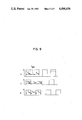
- FIG. 1 is a cross-sectional view diagrammatically illustrating a pulse electrodepositing system for the purpose of explanation of the invention
- FIG. 2 is a graphical representation of experimental results of pulse electrodeposition with the use of the system of FIG. 1;
- FIG. 3 is a diagrammatic cross-sectional view similar to FIG. 1;
- FIG. 4 is a graphical representation of additional experimental results of pulse electrodeposition
- FIGS. 5 to 7 are circuit diagrams of different, preferred circuit assemblies for carrying out the method according to the invention.
- FIG. 8 is a circuit diagram of a further pulsing system embodying the present invention.
- FIG. 9 is a schematic view illustrating waveforms of pulses modified in accordance with a specific aspect of the invention.
- FIG. 1 there is shown a workpiece or substrate 1 having a recess 1a of the depth D and width H to be deposited.
- An electrode 2 is juxtaposed with the workpiece 1 and shown having a bore and opening 2a through which a liquid electrolyte 3 is supplied to the region of the workpiece 1 by a pump (not shown) at a high flow rate.
- a gap spacing formed between the workpiece 1 and the electrode is generally maintained constant by a control unit as described, for example, in Japanese Patent Specification No. 38-12823 published July 22, 1963.
- Terminals 4 are shown which apply a series of electric pulses across the workpiece 1 and the electrode 2, the pulses having a pulse duration or on-time not greater than 100 microseconds, preferably between 1 and 50 microseconds and more preferably 1 and 10 microseconds.
- the pulse interval or off-time should preferably be in excess of two times longer than the pulse on-time.
- a uniform layer 5 is formed electrolytically for a recessed workpiece having D/H ratio as great as 10/1.
- FIG. 2 shows results of experimentation in the form of a graph in which the D/H ratio of a coating obtainable is plotted along the ordinate with respect of the pulse duration or on-time ⁇ on plotted along the abscissa in microseconds.
- the electrolyte used was sulfonic nickel and the gap between the workpiece surface and the electrode maintained at 40 mm with a current density of 5 amperes/cm 2 .
- curves a, b, c, d, e and f are results of pulse deposition under the following conditions, respectively:
- FIG. 3 represents an embodiment of the invention similar to that of FIG. 1.
- Workpieces had a depth of 20 mm and a width of 20 mm.
- the electrode 2 was positioned 10 mm apart from the workpiece 1.
- the electrolyte contained 220 grams/liter of CuSO 4 and 70 grams/liter of H 2 SO 4 and had a temperature of 25° C.
- Pulses had an on/off ratio of 1/30 and a current density of 12 amperes/dm 2 .
- the thickness of the deposited layer on the upper surface S and the thickness of the deposited layer on the bottom of the recess D' were measured. The results are shown in FIG.
- the graphs show that the ratio S/D' is approximately 1 with pulses of a duration or on-time ranging between 0.1 and 10 microseconds and sharply increases when the pulse duration or on-time exceeds 50 microseconds, making it difficult to obtain a deposition in a recess.
- the deposition efficiency is improved as the pulse duration or on-time is increased. Accordingly, best results are obtainable when a pulse duration or on-time is chosen in a range between 1 and 50 microseconds.
- FIGS. 5 to 7 there are shown several circuit arrangements adapted to carry out the method according to the invention and described hereinbefore.
- the circuitry of FIG. 5 includes input terminals 10a and 10b fed from a commercial power source of an alternating current and a voltage regulator 11 adapted to provide across its output terminal the direct-current voltage or output of a constant amplitude.
- the voltage regulator 11 may be any of those known in the art and may be an arrangement described, for example, in U.S. Pat. No. 3,947,753 or in U.S. patents cited therein as references.
- a switch 12 may be constituted by a transistor as shown, a thyrister or any other electronic switching element, and a depositing gap G formed by an electrode 13 and a workpiece 14 juxtaposed in a depositing bath of electrolyte 15.
- a pump not shown
- conduits not shown
- the switch 12 is turned on and off by a pulser 16 which provides control pulses of a preset on time and off time in the ranges described hereinbefore to provide across the electrode 13 and the workpiece 14 the depositing current in the form of pulses basically of the corresponding on time and off time and of an amplitude adjusted by the resistor R.
- the pulsed electrodepositing current is modified as a function of variation of the depositing condition.
- the amplitude, on time and/or off time of depositing pulses may be controlled as a function of the gap voltage, current and/or the impedance between the electrode 13 and the workpiece 14 subject to change in accordance with change in the electro-depositing condition.
- the circuitry of FIG. 5 is designed to respond to the gap current and, to this end, is provided with a sensing resistor 18 inserted in series with the switch 12 and the electrodepositing gap G between the electrode 13 and the workpiece 14.
- the sensing resistor 18 has an amplifier 19 connected at its output.
- the output of the amplifier 19 is connected to the first input 17a of an AND gate 17 having the second input 17b which receives control pulses from the pulser 16.
- the amplifier 19 here has a function to discriminate the magnitude of the gap or electrodepositing current detected by the resistor 18 with respect to a preset value so that, for example, when the gap current exceeds this value, an "0" signal develops to be applied to the first input 17a to block the passage and application of control pulses from the pulser 16 to the switch 12 thereby reducing the frequency or the on/off time ratio of the pulses applied across the electrodepositing gap G.
- the result is the enhanced uniformity of a coating electrodeposited on the workpiece 14.
- the circuitry of FIG. 6 makes use of a chopper amplifier 20 associated with a reference-voltage source 21 and a sensing resistor 18.
- the comparison of the reference voltage 21 with the voltage developed across the resistor 18 in response to the magnitude of the electrodepositing current passing between the electrode 13 and the workpiece causes the amplifier 10 to controllingly turn on and off the switch 12 at a variable on/off times as in the embodiment of FIG. 5.
- the chopper amplifier any of those known may be used; for example, Texas Instruments Regulating Pulse Width Modulators Types SG1524, SG2524, SG3524.
- a multivibrator 22 of known construction is used as the pulser for applying basic switching control pulses to the switch 12.
- the basic switching control pulses and hence the electrodepositing current pulses determined thereby are modified as in the previous embodiments, here by a comparison network 23 which compares the reference voltage which develops across a Zener diode 24 with the voltage across the sensing resistor 8 responding to the magnitude of the electro-depositing current passing through the gap G.
- FIG. 8 there is shown a different circuitry for carrying out the invention.
- the electrode 13 and the workpiece 14 forming an electrodepositing gap G therebetween are connected in series with an electronic switch 12, here shown by three transistors 13a, 13b and 13c, and a direct-current source 11.
- the switch 13 is turned on and off by a pulser 16 which may be a multivibrator having time-determining means 16' here constituted by three pairs of transistor and resistors 16a, 16b and 16c, connected parallel with one another and selectively actuatable.
- a pulser 16 which may be a multivibrator having time-determining means 16' here constituted by three pairs of transistor and resistors 16a, 16b and 16c, connected parallel with one another and selectively actuatable.
- the resistance of the resistors in these pairs is set at different values so that when the network 16a is switched on, the pulse off-time of the pulser 16 has a minimum value; when the network 16c is switched on, it has a maximum value; and when the network 16b is switched on, the same has a medium value.
- the pulser 16 there are provided three gates 17a, 17b and 17c for applying it to the three switching transistors 12a, 12b and 12c, respectively. These gates have each an additional input terminal a, b, c and are each enabled when the corresponding input appears.
- the switches 12a, 12b and 12c are further associated, respectively, in series with resistors R1, R2 and R3 having different resistances which determine tha magnitude of the current pulses applied to the gap.
- the series circuit of an auxiliary voltage source 26 and a transistor 27 is connected across the gap G.
- the transistor 27 is here designed to be tuned on and off by the phase-reversed signals of the output pulses from the pulser 16 appearing across a phase-reversing transistor 31 so that the voltage from the auxiliary source 26 which serves as a test voltage develops across the gap during each off-time of electro-depositing current pulses.
- the resistance or impedance during the pulse off-time is thus selectively detected at a further resistor 28 which is shunted during pulse on-time by a further transistor 29 that is switched on by the on-pulse from the pulser 16.
- the detecting resistor 28 is led to a discriminator unit 30 consisting of three threshold circuits 30a, 30b and 30c which may be constituted by Schmit-trigger circuits having different threshold or triggering voltage levels V30a>V30b>V30c and having output terminals a, b and c, respectively.
- the switch 27 is turned on to permit the test voltage from the source 26 to be applied across the gap G while the switch 29 is turned off.
- a voltage proportional to the gap voltage then develops across the resistor 28 and is discriminated by the discriminator 30.
- a "1" signal will appear at the output b to turn on the switch 16b thereby setting the pulse off-time at a predetermined, moderate value.
- the "1" signal at the output b will selectively enable the gate 17b to permit the switch 12b alone to operate.
- the pulsed electrodepositing current will then flow which has a magnitude established by the resistor R2.
- a "1" signal When the gap is under a high-impedance condition, a "1" signal will develop at the output a to actuate the setting channel 16a thereby setting the pulse off-time at a predetermined, decreased value established by this channel.
- the "1" signal at the output a will also selectively enable the gate 17a to permit the switch 12a alone to be switch-controlled.
- the pulsed electrodepositing current wil then flow which has an increased magnitude established by the resistor R1.
- a series of pulses modified when the gap is under a high-impedance condition are shown at A in FIG. 9.
- a "1" signal When the gap is under a low-impedance condition, a "1" signal will develop at the output c to actuate the setting channel 16c thereby setting the pulse off-time at a predetermined, increased value established by this channel. Simultaneously, the "1" signal at the output c will act to selectively enable the gate 17c to permit the switch 12c alone to be triggered. The pulsed electrodepositing current will then flow which has a decreased magnitude established by the resistor R3.
- a series of pulses modified when the gap is under a low-impedance condition is represented at C in FIG. 9.
- the waveform B in the same FIGURE represents a series of pulses under a normal gap condition.
- Electrodeposition of copper was conducted using a pulsing circuit arrangement as described with reference to FIGS. 8 and 9 and excellent results were obtained, for instance, with a pulse on-time of 10 microseconds and a pluse off/on time ratio of 1/1 under a normal-impedance gap condition, an increased off/on time ratio of 5/1 under a low-impedance gap condition and a decreased off/on time ratio of 0.3/1 under a high-impedance gap condition.
Landscapes
- Engineering & Computer Science (AREA)
- Chemical & Material Sciences (AREA)
- Chemical Kinetics & Catalysis (AREA)
- Electrochemistry (AREA)
- Materials Engineering (AREA)
- Metallurgy (AREA)
- Organic Chemistry (AREA)
- Automation & Control Theory (AREA)
- Power Engineering (AREA)
- Electroplating Methods And Accessories (AREA)
- Electrolytic Production Of Metals (AREA)
- Electrical Discharge Machining, Electrochemical Machining, And Combined Machining (AREA)
Abstract
Electrodeposition is carried out using an electric current which is applied in the form of pulses between a workpiece and an electrode in an electrolyte from which metal is to be deposited upon the workpiece. The pulses have a pulse duration not greater than 100 microseconds and the pulse duration is preferably between 1-50 microseconds while the off time or interval between adjacent pulses is more than twice as long as the on time of the pulses.
Description
This is a continuation of application Ser. No. 828,902, filed Aug. 29, 1977 and now abandoned.
The present invention relates to an improved method of electrodeposition and an apparatus for carrying out the method.
There has become known in the art a pulse depositing method in which an electric current in the form of a series of pulses is passed between a substrate or workpiece and an electrode spacedly juxtaposed therewith in the presence of an electrolyte. Such pulse depositing techniques are described, for example, in Japanese Patent Specifications No. 40-8801 published May 8, 1965 and No. 48-5529 published Feb. 17, 1973. As noted therein, pulse depositing is advantageous in that it enables an efficient ion-control in the depositing electrolyte which permits the deposition process to be achieved at an increased rate and precision. These effects are further enhanced when the liquid electrolyte is supplied so as to pass through the depositing zone at an elevated flow rate, thereby permitting the deposition to be carried out at an increased current density.
The pulse duration of pulses used heretofore in the pulse depositing process is relatively long because of the use of a power supply of commercial output frequency and no practical recognition has been made of the criticality of the pulse on-time, off-time and/or frequency.
This invention is based upon the discovery that improved deposition results are obtained when parameters of pulses are selected in certain ranges. The electrodeposition on surfaces even of a deep recess is thereby achieved with a uniformity, which has heretofore been possible only by electroless or chemical plating techniques requiring a relatively long period of time.
In accordance with the present invention, there is provided a method of electrodeposition in which an electric current in the form of pulses is applied between a workpiece and an electrode juxtaposed therewith in the presence of a liquid electrolyte to form an electrolytically deposited layer on the workpiece, the pulses having a pulse duration not greater than 100 microseconds.
The pulse duration should preferably range between 1 and 50 microseconds. The pulse off-time should preferably be more than two times longer than the pulse on-time.
The flow rate of the electrolyte in the region of electrodeposition should preferably be in excess of 5 meters/second.
Preferably, a pulse of the reverse polarity is supplied between the adjacent pulses of the normal polarity.
An apparatus for carrying out the method according to the invention may comprise a direct-current source, a switching unit for on/off controlling the output of the direct-current source and a pulser for supplying switching control pulses to the switching unit. The direct-current source may preferably comprise a voltage stabilizing regulator.
The apparatus preferably includes means for responding to an electrical parameter representative of the condition of the electrodepositing gap between the electrode and the workpiece. Such means may be a resistor connected in series with the gap and a voltage source to detect the magnitude of the electrodepositing current passing through the gap or a resistor connected in parallel with the electrodepositing gap to detect the voltage thereacross.
The electrical signal representative of the gap condition may be used to modify the basic switching control pulses in the manner to alter a parameter of the electrodepositing current pulses, i.e. pulse on time, off time and/or amplitude, in accordance with the gap condition so that the electrodepositing operation may proceed under an optimum condition.
The electronic switch may thus include at its input or control electrodes gate means having two input terminals, one receiving basic switching control pulses fed from the pulser and the other receiving a control signal fed from the gap-condition detector means to apply modified pulses across the gap. Alternatively, the pulser may incorporate a plurality of time-constant networks determining the on-time and/or off-time of pulses and selectively actuatable in response to the gap-condition detecting means.
Certain embodiments of the invention will now be described with reference to the accompanying drawing in which:
FIG. 1 is a cross-sectional view diagrammatically illustrating a pulse electrodepositing system for the purpose of explanation of the invention;
FIG. 2 is a graphical representation of experimental results of pulse electrodeposition with the use of the system of FIG. 1;
FIG. 3 is a diagrammatic cross-sectional view similar to FIG. 1;
FIG. 4 is a graphical representation of additional experimental results of pulse electrodeposition;
FIGS. 5 to 7 are circuit diagrams of different, preferred circuit assemblies for carrying out the method according to the invention.
FIG. 8 is a circuit diagram of a further pulsing system embodying the present invention; and
FIG. 9 is a schematic view illustrating waveforms of pulses modified in accordance with a specific aspect of the invention.
Referring now to FIG. 1, there is shown a workpiece or substrate 1 having a recess 1a of the depth D and width H to be deposited. An electrode 2 is juxtaposed with the workpiece 1 and shown having a bore and opening 2a through which a liquid electrolyte 3 is supplied to the region of the workpiece 1 by a pump (not shown) at a high flow rate. A gap spacing formed between the workpiece 1 and the electrode is generally maintained constant by a control unit as described, for example, in Japanese Patent Specification No. 38-12823 published July 22, 1963. Terminals 4 are shown which apply a series of electric pulses across the workpiece 1 and the electrode 2, the pulses having a pulse duration or on-time not greater than 100 microseconds, preferably between 1 and 50 microseconds and more preferably 1 and 10 microseconds. The pulse interval or off-time should preferably be in excess of two times longer than the pulse on-time.
Under such conditions, a uniform layer 5 is formed electrolytically for a recessed workpiece having D/H ratio as great as 10/1.
FIG. 2 shows results of experimentation in the form of a graph in which the D/H ratio of a coating obtainable is plotted along the ordinate with respect of the pulse duration or on-time τon plotted along the abscissa in microseconds. The electrolyte used was sulfonic nickel and the gap between the workpiece surface and the electrode maintained at 40 mm with a current density of 5 amperes/cm2. In the graph, curves a, b, c, d, e and f are results of pulse deposition under the following conditions, respectively:
______________________________________
(a) Ton/Toff = 1/2
(b) Ton/Toff = 1/3
(c) Ton/Toff = 1/4
(d) Ton/Toff = 1/4 with the rate of flow of the electrolyte of 3 m/sec.
(e) Ton/Toff = 1/4 with the rate of flow of the electrolyte of 5 m/sec.
(f) Ton/Toff = 1/4 with the rate of flow of the electrolyte of 7
______________________________________
    m/sec.
For each curve, it is seen that with the decrease of the pulse duration or on-time, the value D/H increases and this tendency becomes remarkable with pulses having as low a duration as 100 microseconds. It is also seen that the value D/H increases as the pulse on/off ratio is increased and when this ratio is down to less than 1/2, no appreciable effect is found from the use of pulses. As is noted further, the value D/H increases with longer pulse off-time for a given pulse on-time. The curves d, e and f indicate that the flushing of the electrolyte gives better results, this tendency becoming remarkable when the flow rate is increased to 5 m/sec.
FIG. 3 represents an embodiment of the invention similar to that of FIG. 1. With such system, tests were conducted. Workpieces had a depth of 20 mm and a width of 20 mm. The electrode 2 was positioned 10 mm apart from the workpiece 1. The electrolyte contained 220 grams/liter of CuSO4 and 70 grams/liter of H2 SO4 and had a temperature of 25° C. Pulses had an on/off ratio of 1/30 and a current density of 12 amperes/dm2. To determine the uniformity of the electrodeposition over the entire surface, the thickness of the deposited layer on the upper surface S and the thickness of the deposited layer on the bottom of the recess D' were measured. The results are shown in FIG. 4 in the form of graphs in which the ratio S/D and the deposition efficiency η are plotted along the ordinate with respect to the pulse on-time (microseconds) plotted along the abscissa. Dotted curves represent results in the case in which a reverse-polarity pulse is interposed in each interval between successive regular-polarity pulses.
The graphs show that the ratio S/D' is approximately 1 with pulses of a duration or on-time ranging between 0.1 and 10 microseconds and sharply increases when the pulse duration or on-time exceeds 50 microseconds, making it difficult to obtain a deposition in a recess. On the other hand, the deposition efficiency is improved as the pulse duration or on-time is increased. Accordingly, best results are obtainable when a pulse duration or on-time is chosen in a range between 1 and 50 microseconds.
In FIGS. 5 to 7 there are shown several circuit arrangements adapted to carry out the method according to the invention and described hereinbefore.
The circuitry of FIG. 5 includes input terminals 10a and 10b fed from a commercial power source of an alternating current and a voltage regulator 11 adapted to provide across its output terminal the direct-current voltage or output of a constant amplitude. The voltage regulator 11 may be any of those known in the art and may be an arrangement described, for example, in U.S. Pat. No. 3,947,753 or in U.S. patents cited therein as references.
Connected in series with the output terminals 11a and 11b of the voltage regulator 11 are a current limiting resistor R, a switch 12 may be constituted by a transistor as shown, a thyrister or any other electronic switching element, and a depositing gap G formed by an electrode 13 and a workpiece 14 juxtaposed in a depositing bath of electrolyte 15. To cause the depositing electrolyte to forcibly flow in the region of the gap G, a pump (not shown) and conduits (not shown) for coupling it with the bath 15 may be provided.
The switch 12 is turned on and off by a pulser 16 which provides control pulses of a preset on time and off time in the ranges described hereinbefore to provide across the electrode 13 and the workpiece 14 the depositing current in the form of pulses basically of the corresponding on time and off time and of an amplitude adjusted by the resistor R.
In accordance with a specific aspect of this invention, the pulsed electrodepositing current is modified as a function of variation of the depositing condition. Thus, the amplitude, on time and/or off time of depositing pulses may be controlled as a function of the gap voltage, current and/or the impedance between the electrode 13 and the workpiece 14 subject to change in accordance with change in the electro-depositing condition.
The circuitry of FIG. 5 is designed to respond to the gap current and, to this end, is provided with a sensing resistor 18 inserted in series with the switch 12 and the electrodepositing gap G between the electrode 13 and the workpiece 14. The sensing resistor 18 has an amplifier 19 connected at its output. The output of the amplifier 19 is connected to the first input 17a of an AND gate 17 having the second input 17b which receives control pulses from the pulser 16. The amplifier 19 here has a function to discriminate the magnitude of the gap or electrodepositing current detected by the resistor 18 with respect to a preset value so that, for example, when the gap current exceeds this value, an "0" signal develops to be applied to the first input 17a to block the passage and application of control pulses from the pulser 16 to the switch 12 thereby reducing the frequency or the on/off time ratio of the pulses applied across the electrodepositing gap G. The result is the enhanced uniformity of a coating electrodeposited on the workpiece 14.
The circuitry of FIG. 6 makes use of a chopper amplifier 20 associated with a reference-voltage source 21 and a sensing resistor 18. The comparison of the reference voltage 21 with the voltage developed across the resistor 18 in response to the magnitude of the electrodepositing current passing between the electrode 13 and the workpiece causes the amplifier 10 to controllingly turn on and off the switch 12 at a variable on/off times as in the embodiment of FIG. 5. For the chopper amplifier, any of those known may be used; for example, Texas Instruments Regulating Pulse Width Modulators Types SG1524, SG2524, SG3524.
In the circuitry of FIG. 7, a multivibrator 22 of known construction is used as the pulser for applying basic switching control pulses to the switch 12. The basic switching control pulses and hence the electrodepositing current pulses determined thereby are modified as in the previous embodiments, here by a comparison network 23 which compares the reference voltage which develops across a Zener diode 24 with the voltage across the sensing resistor 8 responding to the magnitude of the electro-depositing current passing through the gap G.
In FIG. 8 there is shown a different circuitry for carrying out the invention. In this circuit arrangement as well, the electrode 13 and the workpiece 14 forming an electrodepositing gap G therebetween are connected in series with an electronic switch 12, here shown by three transistors 13a, 13b and 13c, and a direct-current source 11. The switch 13 is turned on and off by a pulser 16 which may be a multivibrator having time-determining means 16' here constituted by three pairs of transistor and resistors 16a, 16b and 16c, connected parallel with one another and selectively actuatable. The resistance of the resistors in these pairs is set at different values so that when the network 16a is switched on, the pulse off-time of the pulser 16 has a minimum value; when the network 16c is switched on, it has a maximum value; and when the network 16b is switched on, the same has a medium value.
At the output of the pulser 16 there are provided three gates 17a, 17b and 17c for applying it to the three switching transistors 12a, 12b and 12c, respectively. These gates have each an additional input terminal a, b, c and are each enabled when the corresponding input appears. The switches 12a, 12b and 12c are further associated, respectively, in series with resistors R1, R2 and R3 having different resistances which determine tha magnitude of the current pulses applied to the gap.
In this embodiment, the series circuit of an auxiliary voltage source 26 and a transistor 27 is connected across the gap G. The transistor 27 is here designed to be tuned on and off by the phase-reversed signals of the output pulses from the pulser 16 appearing across a phase-reversing transistor 31 so that the voltage from the auxiliary source 26 which serves as a test voltage develops across the gap during each off-time of electro-depositing current pulses. The resistance or impedance during the pulse off-time is thus selectively detected at a further resistor 28 which is shunted during pulse on-time by a further transistor 29 that is switched on by the on-pulse from the pulser 16. The detecting resistor 28 is led to a discriminator unit 30 consisting of three threshold circuits 30a, 30b and 30c which may be constituted by Schmit-trigger circuits having different threshold or triggering voltage levels V30a>V30b>V30c and having output terminals a, b and c, respectively.
In operation, every time the depositing current is switched off, the switch 27 is turned on to permit the test voltage from the source 26 to be applied across the gap G while the switch 29 is turned off. A voltage proportional to the gap voltage then develops across the resistor 28 and is discriminated by the discriminator 30. Thus, when the gap is under a normal condition, a "1" signal will appear at the output b to turn on the switch 16b thereby setting the pulse off-time at a predetermined, moderate value. At the same time, the "1" signal at the output b will selectively enable the gate 17b to permit the switch 12b alone to operate. The pulsed electrodepositing current will then flow which has a magnitude established by the resistor R2.
When the gap is under a high-impedance condition, a "1" signal will develop at the output a to actuate the setting channel 16a thereby setting the pulse off-time at a predetermined, decreased value established by this channel. The "1" signal at the output a will also selectively enable the gate 17a to permit the switch 12a alone to be switch-controlled. The pulsed electrodepositing current wil then flow which has an increased magnitude established by the resistor R1. A series of pulses modified when the gap is under a high-impedance condition are shown at A in FIG. 9.
When the gap is under a low-impedance condition, a "1" signal will develop at the output c to actuate the setting channel 16c thereby setting the pulse off-time at a predetermined, increased value established by this channel. Simultaneously, the "1" signal at the output c will act to selectively enable the gate 17c to permit the switch 12c alone to be triggered. The pulsed electrodepositing current will then flow which has a decreased magnitude established by the resistor R3. A series of pulses modified when the gap is under a low-impedance condition is represented at C in FIG. 9. The waveform B in the same FIGURE represents a series of pulses under a normal gap condition.
Electrodeposition of copper was conducted using a pulsing circuit arrangement as described with reference to FIGS. 8 and 9 and excellent results were obtained, for instance, with a pulse on-time of 10 microseconds and a pluse off/on time ratio of 1/1 under a normal-impedance gap condition, an increased off/on time ratio of 5/1 under a low-impedance gap condition and a decreased off/on time ratio of 0.3/1 under a high-impedance gap condition.
Claims (8)
1. A method of electrodepositing a metal upon a workpiece from an electrolyte, said method comprising the steps of:
juxtaposing a surface of said workpiece formed with a recess having a depth D and a width H with an electrode having an electrode surface extending over the opening of said recess and disposed outside the recess;
flushing the electrolyte in the region of said electrode surface past said surfaces and through said recess; and
applying an electric current poled to electrodeposit metal from said electrolyte upon said workpiece and in the recess thereof to a uniform thickness, the ratio D/H being greater than 1/1 and up to 10/1, said electric current being passed through said electrode, said electrolyte and said workpiece in the form of pulses having a pulse duration between 1 and 50 microseconds.
2. The method defined in claim 1 wherein the interval between adjacent pulses is more than twice as long as the pulse duration.
3. The method defined in claim 1, further comprising the step of interposing a reverse-polarity pulse between the successive pulses of the electrodepositing polarity.
4. The method defined in claim 1 wherein at least one parameter of the electric current is modified in response to at least one electrical parameter representing the condition of the gap between the electrode and the workpiece.
5. The method defined in claim 4 wherein said parameter of said electric current is selected from the group which consists of pulse duration, pulse interval and pulse amplitude.
6. The method defined in claim 5 wherein said gap-condition parameter is selected from the group which consists of gap current, gap voltage and gap impedance.
7. The method defined in claim 1 for the deposition of a layer on the surface surrounding said recess to a thickness S and a layer on the bottom of said recess to a thickness of D', wherein the ratio S/D' is approximately 1, the pulse duration being maintained in the range between 1 and 10 microseconds.
8. The method defined in claim 1 wherein said electrolyte is flushed in the region of electrodeposition at a flow rate in excess of 5 meters per second.
Applications Claiming Priority (6)
| Application Number | Priority Date | Filing Date | Title |
|---|---|---|---|
| JP51-104724 | 1976-09-01 | ||
| JP10472476A JPS5329346A (en) | 1976-09-01 | 1976-09-01 | Process of electrodeposition |
| JP51-150051 | 1976-12-14 | ||
| JP15005176A JPS5373437A (en) | 1976-12-14 | 1976-12-14 | Power source device for electrolysis |
| JP6912977A JPS544253A (en) | 1977-06-10 | 1977-06-10 | Electrolytic apparatus |
| JP52-69129 | 1977-06-10 |
Related Parent Applications (1)
| Application Number | Title | Priority Date | Filing Date |
|---|---|---|---|
| US05828902 Continuation | 1977-08-29 |
Publications (1)
| Publication Number | Publication Date |
|---|---|
| US4496436A true US4496436A (en) | 1985-01-29 |
Family
ID=27299961
Family Applications (1)
| Application Number | Title | Priority Date | Filing Date |
|---|---|---|---|
| US06/973,608 Expired - Lifetime US4496436A (en) | 1976-09-01 | 1978-12-27 | Pulse electrodepositing method |
Country Status (5)
| Country | Link |
|---|---|
| US (1) | US4496436A (en) |
| CH (1) | CH629542A5 (en) |
| DE (1) | DE2739427C2 (en) |
| FR (1) | FR2363644A1 (en) |
| GB (1) | GB1529187A (en) |
Cited By (28)
| Publication number | Priority date | Publication date | Assignee | Title |
|---|---|---|---|---|
| US4566953A (en) * | 1984-12-24 | 1986-01-28 | At&T Technologies, Inc. | Pulse plating of nickel-antimony films |
| EP0330722A1 (en) * | 1988-03-04 | 1989-09-06 | ELCA S.r.l. | Electrochemical process for producing platings of chromium and similar metals, by means of pulsating current with periodic reversing polarity, and relevant equipment |
| EP0457339A2 (en) * | 1990-05-18 | 1991-11-21 | Sorlet Finland Oy | Method and apparatus for the production of circuit boards |
| US5270229A (en) * | 1989-03-07 | 1993-12-14 | Matsushita Electric Industrial Co., Ltd. | Thin film semiconductor device and process for producing thereof |
| US5705230A (en) * | 1992-03-17 | 1998-01-06 | Ebara Corporation | Method for filling small holes or covering small recesses in the surface of substrates |
| EP1191129A2 (en) * | 2000-08-29 | 2002-03-27 | SOQI Inc. | Metal plating method |
| US6379223B1 (en) | 1999-11-29 | 2002-04-30 | Applied Materials, Inc. | Method and apparatus for electrochemical-mechanical planarization |
| US6402931B1 (en) | 1998-05-18 | 2002-06-11 | Faraday Technology Marketing Group, Llc | Electrochemical machining using modulated reverse electric fields |
| US6582578B1 (en) | 1999-04-08 | 2003-06-24 | Applied Materials, Inc. | Method and associated apparatus for tilting a substrate upon entry for metal deposition |
| US20030152293A1 (en) * | 2002-01-24 | 2003-08-14 | Joel Bresler | Method and system for locating position in printed texts and delivering multimedia information |
| US20030188974A1 (en) * | 2002-04-03 | 2003-10-09 | Applied Materials, Inc. | Homogeneous copper-tin alloy plating for enhancement of electro-migration resistance in interconnects |
| US20030201166A1 (en) * | 2002-04-29 | 2003-10-30 | Applied Materials, Inc. | method for regulating the electrical power applied to a substrate during an immersion process |
| US20030201185A1 (en) * | 2002-04-29 | 2003-10-30 | Applied Materials, Inc. | In-situ pre-clean for electroplating process |
| US20030209523A1 (en) * | 2002-05-09 | 2003-11-13 | Applied Materials, Inc. | Planarization by chemical polishing for ULSI applications |
| US20030209443A1 (en) * | 2002-05-09 | 2003-11-13 | Applied Materials, Inc. | Substrate support with fluid retention band |
| US20040072445A1 (en) * | 2002-07-11 | 2004-04-15 | Applied Materials, Inc. | Effective method to improve surface finish in electrochemically assisted CMP |
| US6740221B2 (en) | 2001-03-15 | 2004-05-25 | Applied Materials Inc. | Method of forming copper interconnects |
| US20040118699A1 (en) * | 2002-10-02 | 2004-06-24 | Applied Materials, Inc. | Homogeneous copper-palladium alloy plating for enhancement of electro-migration resistance in interconnects |
| US20040206628A1 (en) * | 2003-04-18 | 2004-10-21 | Applied Materials, Inc. | Electrical bias during wafer exit from electrolyte bath |
| US6808612B2 (en) | 2000-05-23 | 2004-10-26 | Applied Materials, Inc. | Method and apparatus to overcome anomalies in copper seed layers and to tune for feature size and aspect ratio |
| US6913680B1 (en) | 2000-05-02 | 2005-07-05 | Applied Materials, Inc. | Method of application of electrical biasing to enhance metal deposition |
| US7077725B2 (en) | 1999-11-29 | 2006-07-18 | Applied Materials, Inc. | Advanced electrolytic polish (AEP) assisted metal wafer planarization method and apparatus |
| US20060175201A1 (en) * | 2005-02-07 | 2006-08-10 | Hooman Hafezi | Immersion process for electroplating applications |
| US20090236230A1 (en) * | 2004-09-20 | 2009-09-24 | Bert Reents | Galvanic process for filling through-holes with metals, in particular of printed circuit boards with copper |
| US20110017608A1 (en) * | 2009-07-27 | 2011-01-27 | Faraday Technology, Inc. | Electrochemical etching and polishing of conductive substrates |
| US8784634B2 (en) | 2006-03-30 | 2014-07-22 | Atotech Deutschland Gmbh | Electrolytic method for filling holes and cavities with metals |
| US10081880B2 (en) | 2013-05-06 | 2018-09-25 | Fpinnovations | Cellulose nanocrystal (CNC) films and conductive CNC-based polymer films produced using electrochemical techniques |
| US11035051B2 (en) | 2016-08-15 | 2021-06-15 | Atotech Deutschland Gmbh | Acidic aqueous composition for electrolytic copper plating |
Families Citing this family (15)
| Publication number | Priority date | Publication date | Assignee | Title |
|---|---|---|---|---|
| GB1539309A (en) * | 1976-12-14 | 1979-01-31 | Inoue Japax Res | Electrochemical polishing |
| US4396467A (en) * | 1980-10-27 | 1983-08-02 | General Electric Company | Periodic reverse current pulsing to form uniformly sized feed through conductors |
| NL8105150A (en) | 1981-11-13 | 1983-06-01 | Veco Beheer Bv | METHOD FOR MANUFACTURING SCREEN MATERIAL, SCREENING MATERIAL OBTAINED, AND APPARATUS FOR CARRYING OUT THE METHOD |
| US4468293A (en) * | 1982-03-05 | 1984-08-28 | Olin Corporation | Electrochemical treatment of copper for improving its bond strength |
| US4515671A (en) * | 1983-01-24 | 1985-05-07 | Olin Corporation | Electrochemical treatment of copper for improving its bond strength |
| DE4225961C5 (en) * | 1992-08-06 | 2011-01-27 | Atotech Deutschland Gmbh | Apparatus for electroplating, in particular copper plating, flat plate or arched objects |
| DE19545231A1 (en) * | 1995-11-21 | 1997-05-22 | Atotech Deutschland Gmbh | Process for the electrolytic deposition of metal layers |
| DE19547948C1 (en) * | 1995-12-21 | 1996-11-21 | Atotech Deutschland Gmbh | Mfg. unipolar or bipolar pulsed current for plating esp. of circuit boards at high current |
| DE19925373B4 (en) * | 1999-06-02 | 2006-04-06 | Robert Bosch Gmbh | Method and apparatus for electroplating |
| DE10202431C1 (en) * | 2002-01-22 | 2003-05-28 | Egon Huebel | Apparatus for electrochemical metallization, etching, oxidation or reduction of materials uses small electrochemical cells with contact electrodes fed with electrical pulses |
| DE10311575B4 (en) * | 2003-03-10 | 2007-03-22 | Atotech Deutschland Gmbh | Process for the electrolytic metallization of workpieces with high aspect ratio holes |
| ATE506468T1 (en) | 2008-04-28 | 2011-05-15 | Atotech Deutschland Gmbh | AQUEOUS ACID BATH AND METHOD FOR ELECTROLYTIC CUTTING OF COPPER |
| EP2518187A1 (en) | 2011-04-26 | 2012-10-31 | Atotech Deutschland GmbH | Aqueous acidic bath for electrolytic deposition of copper |
| EP3470552B1 (en) | 2017-10-13 | 2020-12-30 | ATOTECH Deutschland GmbH | An acidic aqueous composition for electrolytically depositing a copper deposit |
| EP3901331A1 (en) | 2020-04-23 | 2021-10-27 | ATOTECH Deutschland GmbH | Acidic aqueous composition for electrolytically depositing a copper deposit |
Citations (6)
| Publication number | Priority date | Publication date | Assignee | Title |
|---|---|---|---|---|
| US2726202A (en) * | 1955-06-06 | 1955-12-06 | Robotron Corp | Method for plating by condenser discharge |
| DE1421984A1 (en) * | 1962-10-01 | 1968-11-07 | Forsch Edelmetalle Und Metallc | Process for the production of crack-free chrome coatings |
| DE2061225A1 (en) * | 1969-12-30 | 1971-09-09 | Ibm | Process for the electrolytic deposition of alloyed thin layers |
| FR2134401A1 (en) * | 1971-04-24 | 1972-12-08 | Schering Ag | |
| US3959088A (en) * | 1975-03-19 | 1976-05-25 | The United States Of America As Represented By The Secretary Of The Army | Method and apparatus for generating high amperage pulses from an A-C power source |
| US4049507A (en) * | 1974-09-18 | 1977-09-20 | Sony Corporation | Electrodepositing method |
-
1977
- 1977-08-31 CH CH1062977A patent/CH629542A5/en not_active IP Right Cessation
- 1977-09-01 FR FR7726610A patent/FR2363644A1/en active Granted
- 1977-09-01 DE DE2739427A patent/DE2739427C2/en not_active Expired
- 1977-09-01 GB GB36632/77A patent/GB1529187A/en not_active Expired
-
1978
- 1978-12-27 US US06/973,608 patent/US4496436A/en not_active Expired - Lifetime
Patent Citations (6)
| Publication number | Priority date | Publication date | Assignee | Title |
|---|---|---|---|---|
| US2726202A (en) * | 1955-06-06 | 1955-12-06 | Robotron Corp | Method for plating by condenser discharge |
| DE1421984A1 (en) * | 1962-10-01 | 1968-11-07 | Forsch Edelmetalle Und Metallc | Process for the production of crack-free chrome coatings |
| DE2061225A1 (en) * | 1969-12-30 | 1971-09-09 | Ibm | Process for the electrolytic deposition of alloyed thin layers |
| FR2134401A1 (en) * | 1971-04-24 | 1972-12-08 | Schering Ag | |
| US4049507A (en) * | 1974-09-18 | 1977-09-20 | Sony Corporation | Electrodepositing method |
| US3959088A (en) * | 1975-03-19 | 1976-05-25 | The United States Of America As Represented By The Secretary Of The Army | Method and apparatus for generating high amperage pulses from an A-C power source |
Non-Patent Citations (12)
| Title |
|---|
| A. Kenneth Graham, "Electroplating Engineering Handbook", pp. 573-574, (1955). |
| A. Kenneth Graham, Electroplating Engineering Handbook , pp. 573 574, (1955). * |
| C. C. Wan et al., Plating, pp. 559 564, Jun. 1974. * |
| C. C. Wan et al., Plating, pp. 559-564, Jun. 1974. |
| Heinz W. Dettner et al., "Handbuch der Galvano-Technik", vol. 1, Part 1, p. 135, (1963). |
| Heinz W. Dettner et al., Handbuch der Galvano Technik , vol. 1, Part 1, p. 135, (1963). * |
| V. A. Lamb, Plating, vol. 56, No. 8, pp. 909 913, (1969). * |
| V. A. Lamb, Plating, vol. 56, No. 8, pp. 909-913, (1969). |
| W. A. Wesley et al., Reprint from 36th Annual Proc., Am. Electroplaters Soc., pp. 79 91, (1949). * |
| W. A. Wesley et al., Reprint from 36th Annual Proc., Am. Electroplaters Soc., pp. 79-91, (1949). |
| W. Sullivan, Plating, vol. 62, No. 2, pp. 139 141, (1975). * |
| W. Sullivan, Plating, vol. 62, No. 2, pp. 139-141, (1975). |
Cited By (36)
| Publication number | Priority date | Publication date | Assignee | Title |
|---|---|---|---|---|
| US4566953A (en) * | 1984-12-24 | 1986-01-28 | At&T Technologies, Inc. | Pulse plating of nickel-antimony films |
| EP0330722A1 (en) * | 1988-03-04 | 1989-09-06 | ELCA S.r.l. | Electrochemical process for producing platings of chromium and similar metals, by means of pulsating current with periodic reversing polarity, and relevant equipment |
| US5270229A (en) * | 1989-03-07 | 1993-12-14 | Matsushita Electric Industrial Co., Ltd. | Thin film semiconductor device and process for producing thereof |
| EP0457339A2 (en) * | 1990-05-18 | 1991-11-21 | Sorlet Finland Oy | Method and apparatus for the production of circuit boards |
| EP0457339A3 (en) * | 1990-05-18 | 1993-01-13 | Sorlet Finland Oy | Method and apparatus for the production of circuit boards |
| US5705230A (en) * | 1992-03-17 | 1998-01-06 | Ebara Corporation | Method for filling small holes or covering small recesses in the surface of substrates |
| US6402931B1 (en) | 1998-05-18 | 2002-06-11 | Faraday Technology Marketing Group, Llc | Electrochemical machining using modulated reverse electric fields |
| US6582578B1 (en) | 1999-04-08 | 2003-06-24 | Applied Materials, Inc. | Method and associated apparatus for tilting a substrate upon entry for metal deposition |
| US6379223B1 (en) | 1999-11-29 | 2002-04-30 | Applied Materials, Inc. | Method and apparatus for electrochemical-mechanical planarization |
| US6739951B2 (en) | 1999-11-29 | 2004-05-25 | Applied Materials Inc. | Method and apparatus for electrochemical-mechanical planarization |
| US7077725B2 (en) | 1999-11-29 | 2006-07-18 | Applied Materials, Inc. | Advanced electrolytic polish (AEP) assisted metal wafer planarization method and apparatus |
| US6913680B1 (en) | 2000-05-02 | 2005-07-05 | Applied Materials, Inc. | Method of application of electrical biasing to enhance metal deposition |
| US6808612B2 (en) | 2000-05-23 | 2004-10-26 | Applied Materials, Inc. | Method and apparatus to overcome anomalies in copper seed layers and to tune for feature size and aspect ratio |
| EP1191129A3 (en) * | 2000-08-29 | 2006-05-17 | SOQI Inc. | Metal plating method |
| EP1191129A2 (en) * | 2000-08-29 | 2002-03-27 | SOQI Inc. | Metal plating method |
| US6740221B2 (en) | 2001-03-15 | 2004-05-25 | Applied Materials Inc. | Method of forming copper interconnects |
| US7239747B2 (en) | 2002-01-24 | 2007-07-03 | Chatterbox Systems, Inc. | Method and system for locating position in printed texts and delivering multimedia information |
| US20030152293A1 (en) * | 2002-01-24 | 2003-08-14 | Joel Bresler | Method and system for locating position in printed texts and delivering multimedia information |
| US20030188974A1 (en) * | 2002-04-03 | 2003-10-09 | Applied Materials, Inc. | Homogeneous copper-tin alloy plating for enhancement of electro-migration resistance in interconnects |
| US6911136B2 (en) | 2002-04-29 | 2005-06-28 | Applied Materials, Inc. | Method for regulating the electrical power applied to a substrate during an immersion process |
| US20030201185A1 (en) * | 2002-04-29 | 2003-10-30 | Applied Materials, Inc. | In-situ pre-clean for electroplating process |
| US20030201166A1 (en) * | 2002-04-29 | 2003-10-30 | Applied Materials, Inc. | method for regulating the electrical power applied to a substrate during an immersion process |
| US20030209523A1 (en) * | 2002-05-09 | 2003-11-13 | Applied Materials, Inc. | Planarization by chemical polishing for ULSI applications |
| US7189313B2 (en) | 2002-05-09 | 2007-03-13 | Applied Materials, Inc. | Substrate support with fluid retention band |
| US20030209443A1 (en) * | 2002-05-09 | 2003-11-13 | Applied Materials, Inc. | Substrate support with fluid retention band |
| US20040072445A1 (en) * | 2002-07-11 | 2004-04-15 | Applied Materials, Inc. | Effective method to improve surface finish in electrochemically assisted CMP |
| US20040118699A1 (en) * | 2002-10-02 | 2004-06-24 | Applied Materials, Inc. | Homogeneous copper-palladium alloy plating for enhancement of electro-migration resistance in interconnects |
| US20040206628A1 (en) * | 2003-04-18 | 2004-10-21 | Applied Materials, Inc. | Electrical bias during wafer exit from electrolyte bath |
| US9445510B2 (en) | 2004-09-20 | 2016-09-13 | Atotech Deutschland Gmbh | Galvanic process for filling through-holes with metals, in particular of printed circuit boards with copper |
| US20090236230A1 (en) * | 2004-09-20 | 2009-09-24 | Bert Reents | Galvanic process for filling through-holes with metals, in particular of printed circuit boards with copper |
| US9526183B2 (en) | 2004-09-20 | 2016-12-20 | Atotech Deutschland Gmbh | Galvanic process for filling through-holes with metals, in particular of printed circuit boards with copper |
| US20060175201A1 (en) * | 2005-02-07 | 2006-08-10 | Hooman Hafezi | Immersion process for electroplating applications |
| US8784634B2 (en) | 2006-03-30 | 2014-07-22 | Atotech Deutschland Gmbh | Electrolytic method for filling holes and cavities with metals |
| US20110017608A1 (en) * | 2009-07-27 | 2011-01-27 | Faraday Technology, Inc. | Electrochemical etching and polishing of conductive substrates |
| US10081880B2 (en) | 2013-05-06 | 2018-09-25 | Fpinnovations | Cellulose nanocrystal (CNC) films and conductive CNC-based polymer films produced using electrochemical techniques |
| US11035051B2 (en) | 2016-08-15 | 2021-06-15 | Atotech Deutschland Gmbh | Acidic aqueous composition for electrolytic copper plating |
Also Published As
| Publication number | Publication date |
|---|---|
| FR2363644A1 (en) | 1978-03-31 |
| DE2739427A1 (en) | 1978-03-02 |
| FR2363644B1 (en) | 1982-05-28 |
| GB1529187A (en) | 1978-10-18 |
| CH629542A5 (en) | 1982-04-30 |
| DE2739427C2 (en) | 1983-12-08 |
Similar Documents
| Publication | Publication Date | Title |
|---|---|---|
| US4496436A (en) | Pulse electrodepositing method | |
| US4125444A (en) | Electrochemical polishing method | |
| US5869797A (en) | Bipolar electrical discharge machine which adjusts voltage polarity based on short circuit detection | |
| US6723219B2 (en) | Method of direct electroplating on a low conductivity material, and electroplated metal deposited therewith | |
| US20020169516A1 (en) | Method of controlling an electrochemical machining process | |
| EP0495985B1 (en) | Method and apparatus for electrical discharge machining | |
| US4206028A (en) | Electrochemical polishing system | |
| US5352859A (en) | Adaptive method and apparatus for controlling machining current in electric discharge machines | |
| US5049246A (en) | Electrolytic processing apparatus and method with time multiplexed power supply | |
| US5007993A (en) | Electrolytic processing apparatus and method with time multiplexed power supply | |
| US4392043A (en) | Pulse generator | |
| US3530271A (en) | Electro-erosive working electrode having multiple individually insulated elements | |
| EP0134679B1 (en) | An electroerosive machining method and apparatus | |
| GB1604398A (en) | Electrical discharge machines and methods of electrical discharge machining | |
| DE19708023B4 (en) | Electrode feeder and method for electro-erosive machining | |
| US4719327A (en) | Electrical discharge machining power supply | |
| RU2070947C1 (en) | Method for microarc oxidation of metal articles and device for its embodiment | |
| US4102771A (en) | Measuring device and process for recording on electrodeposition parameters of throwing power | |
| US2741586A (en) | Electroplating metals | |
| SU1664882A1 (en) | Method of measuring average current density in electroplating baths | |
| US4151388A (en) | Current control system for electrical discharge machining apparatus | |
| RU1772221C (en) | Method of automatic control over electrochemical facing thickness | |
| USRE29361E (en) | Process for shaping workpiece by electrical discharge and apparatus therefor | |
| JPS5973226A (en) | Machining power supply of electric discharge machining device | |
| WO1983002786A1 (en) | Method of electroplating |
Legal Events
| Date | Code | Title | Description |
|---|---|---|---|
| STCF | Information on status: patent grant |
Free format text: PATENTED CASE |