US4487828A - Method of manufacturing printed circuit boards - Google Patents
Method of manufacturing printed circuit boards Download PDFInfo
- Publication number
- US4487828A US4487828A US06/500,681 US50068183A US4487828A US 4487828 A US4487828 A US 4487828A US 50068183 A US50068183 A US 50068183A US 4487828 A US4487828 A US 4487828A
- Authority
- US
- United States
- Prior art keywords
- solder
- resist
- substrate
- paths
- pads
- Prior art date
- Legal status (The legal status is an assumption and is not a legal conclusion. Google has not performed a legal analysis and makes no representation as to the accuracy of the status listed.)
- Expired - Lifetime
Links
Images

Classifications
-
- H—ELECTRICITY
- H05—ELECTRIC TECHNIQUES NOT OTHERWISE PROVIDED FOR
- H05K—PRINTED CIRCUITS; CASINGS OR CONSTRUCTIONAL DETAILS OF ELECTRIC APPARATUS; MANUFACTURE OF ASSEMBLAGES OF ELECTRICAL COMPONENTS
- H05K3/00—Apparatus or processes for manufacturing printed circuits
- H05K3/0094—Filling or covering plated through-holes or blind plated vias, e.g. for masking or for mechanical reinforcement
-
- H—ELECTRICITY
- H05—ELECTRIC TECHNIQUES NOT OTHERWISE PROVIDED FOR
- H05K—PRINTED CIRCUITS; CASINGS OR CONSTRUCTIONAL DETAILS OF ELECTRIC APPARATUS; MANUFACTURE OF ASSEMBLAGES OF ELECTRICAL COMPONENTS
- H05K3/00—Apparatus or processes for manufacturing printed circuits
- H05K3/30—Assembling printed circuits with electric components, e.g. with resistor
- H05K3/32—Assembling printed circuits with electric components, e.g. with resistor electrically connecting electric components or wires to printed circuits
- H05K3/34—Assembling printed circuits with electric components, e.g. with resistor electrically connecting electric components or wires to printed circuits by soldering
- H05K3/3457—Solder materials or compositions; Methods of application thereof
- H05K3/3473—Plating of solder
-
- H—ELECTRICITY
- H05—ELECTRIC TECHNIQUES NOT OTHERWISE PROVIDED FOR
- H05K—PRINTED CIRCUITS; CASINGS OR CONSTRUCTIONAL DETAILS OF ELECTRIC APPARATUS; MANUFACTURE OF ASSEMBLAGES OF ELECTRICAL COMPONENTS
- H05K2201/00—Indexing scheme relating to printed circuits covered by H05K1/00
- H05K2201/09—Shape and layout
- H05K2201/09209—Shape and layout details of conductors
- H05K2201/095—Conductive through-holes or vias
- H05K2201/09581—Applying an insulating coating on the walls of holes
-
- H—ELECTRICITY
- H05—ELECTRIC TECHNIQUES NOT OTHERWISE PROVIDED FOR
- H05K—PRINTED CIRCUITS; CASINGS OR CONSTRUCTIONAL DETAILS OF ELECTRIC APPARATUS; MANUFACTURE OF ASSEMBLAGES OF ELECTRICAL COMPONENTS
- H05K2203/00—Indexing scheme relating to apparatus or processes for manufacturing printed circuits covered by H05K3/00
- H05K2203/03—Metal processing
- H05K2203/0361—Stripping a part of an upper metal layer to expose a lower metal layer, e.g. by etching or using a laser
-
- H—ELECTRICITY
- H05—ELECTRIC TECHNIQUES NOT OTHERWISE PROVIDED FOR
- H05K—PRINTED CIRCUITS; CASINGS OR CONSTRUCTIONAL DETAILS OF ELECTRIC APPARATUS; MANUFACTURE OF ASSEMBLAGES OF ELECTRICAL COMPONENTS
- H05K2203/00—Indexing scheme relating to apparatus or processes for manufacturing printed circuits covered by H05K3/00
- H05K2203/07—Treatments involving liquids, e.g. plating, rinsing
- H05K2203/0703—Plating
- H05K2203/0723—Electroplating, e.g. finish plating
-
- H—ELECTRICITY
- H05—ELECTRIC TECHNIQUES NOT OTHERWISE PROVIDED FOR
- H05K—PRINTED CIRCUITS; CASINGS OR CONSTRUCTIONAL DETAILS OF ELECTRIC APPARATUS; MANUFACTURE OF ASSEMBLAGES OF ELECTRICAL COMPONENTS
- H05K2203/00—Indexing scheme relating to apparatus or processes for manufacturing printed circuits covered by H05K3/00
- H05K2203/07—Treatments involving liquids, e.g. plating, rinsing
- H05K2203/0756—Uses of liquids, e.g. rinsing, coating, dissolving
- H05K2203/0759—Forming a polymer layer by liquid coating, e.g. a non-metallic protective coating or an organic bonding layer
-
- H—ELECTRICITY
- H05—ELECTRIC TECHNIQUES NOT OTHERWISE PROVIDED FOR
- H05K—PRINTED CIRCUITS; CASINGS OR CONSTRUCTIONAL DETAILS OF ELECTRIC APPARATUS; MANUFACTURE OF ASSEMBLAGES OF ELECTRICAL COMPONENTS
- H05K3/00—Apparatus or processes for manufacturing printed circuits
- H05K3/0073—Masks not provided for in groups H05K3/02 - H05K3/46, e.g. for photomechanical production of patterned surfaces
- H05K3/0082—Masks not provided for in groups H05K3/02 - H05K3/46, e.g. for photomechanical production of patterned surfaces characterised by the exposure method of radiation-sensitive masks
-
- H—ELECTRICITY
- H05—ELECTRIC TECHNIQUES NOT OTHERWISE PROVIDED FOR
- H05K—PRINTED CIRCUITS; CASINGS OR CONSTRUCTIONAL DETAILS OF ELECTRIC APPARATUS; MANUFACTURE OF ASSEMBLAGES OF ELECTRICAL COMPONENTS
- H05K3/00—Apparatus or processes for manufacturing printed circuits
- H05K3/02—Apparatus or processes for manufacturing printed circuits in which the conductive material is applied to the surface of the insulating support and is thereafter removed from such areas of the surface which are not intended for current conducting or shielding
- H05K3/06—Apparatus or processes for manufacturing printed circuits in which the conductive material is applied to the surface of the insulating support and is thereafter removed from such areas of the surface which are not intended for current conducting or shielding the conductive material being removed chemically or electrolytically, e.g. by photo-etch process
- H05K3/061—Etching masks
- H05K3/062—Etching masks consisting of metals or alloys or metallic inorganic compounds
-
- H—ELECTRICITY
- H05—ELECTRIC TECHNIQUES NOT OTHERWISE PROVIDED FOR
- H05K—PRINTED CIRCUITS; CASINGS OR CONSTRUCTIONAL DETAILS OF ELECTRIC APPARATUS; MANUFACTURE OF ASSEMBLAGES OF ELECTRICAL COMPONENTS
- H05K3/00—Apparatus or processes for manufacturing printed circuits
- H05K3/10—Apparatus or processes for manufacturing printed circuits in which conductive material is applied to the insulating support in such a manner as to form the desired conductive pattern
- H05K3/108—Apparatus or processes for manufacturing printed circuits in which conductive material is applied to the insulating support in such a manner as to form the desired conductive pattern by semi-additive methods; masks therefor
-
- H—ELECTRICITY
- H05—ELECTRIC TECHNIQUES NOT OTHERWISE PROVIDED FOR
- H05K—PRINTED CIRCUITS; CASINGS OR CONSTRUCTIONAL DETAILS OF ELECTRIC APPARATUS; MANUFACTURE OF ASSEMBLAGES OF ELECTRICAL COMPONENTS
- H05K3/00—Apparatus or processes for manufacturing printed circuits
- H05K3/30—Assembling printed circuits with electric components, e.g. with resistor
- H05K3/32—Assembling printed circuits with electric components, e.g. with resistor electrically connecting electric components or wires to printed circuits
- H05K3/34—Assembling printed circuits with electric components, e.g. with resistor electrically connecting electric components or wires to printed circuits by soldering
- H05K3/3452—Solder masks
-
- H—ELECTRICITY
- H05—ELECTRIC TECHNIQUES NOT OTHERWISE PROVIDED FOR
- H05K—PRINTED CIRCUITS; CASINGS OR CONSTRUCTIONAL DETAILS OF ELECTRIC APPARATUS; MANUFACTURE OF ASSEMBLAGES OF ELECTRICAL COMPONENTS
- H05K3/00—Apparatus or processes for manufacturing printed circuits
- H05K3/40—Forming printed elements for providing electric connections to or between printed circuits
- H05K3/42—Plated through-holes or plated via connections
- H05K3/425—Plated through-holes or plated via connections characterised by the sequence of steps for plating the through-holes or via connections in relation to the conductive pattern
- H05K3/427—Plated through-holes or plated via connections characterised by the sequence of steps for plating the through-holes or via connections in relation to the conductive pattern initial plating of through-holes in metal-clad substrates
Definitions
- This invention relates to methods of manufacturing printed circuit boards and in particular to a method of manufacturing fine line printed wiring boards.
- Printed circuit boards are almost universally used in the electronics industry to mount electrical components and to interconnect these components by means of copper conductor paths printed, or laid, on the board surface. As components are being created which perform more functions while also designed in more compact arrangements thus allowing more components to be positioned on a board surface, the number of copper conductor paths, or traces, required to operate these miniaturized powerful components has not only grown substantially, but the path layouts have also become more complex. Printed circuit board manufacturers have attempted to meet these design demands for more component circuit configurations per board by incorporating new manufacturing techniques which have permitted thinner copper conductors to be laid on the board surface.
- solder mask To operate effectively, the solder mask must completely cover each conductor path and also cover the board surfaces between the paths to inhibit solder flow between the paths.
- the space between the paths is so narrow that the gelatinous fluid can not flow down between the conductor paths to cover the interpath board surface but instead either forms a bridge between the paths and over the interpath surface, or is missing entirely from the interpath surface.
- the solder layer on the conductor path becomes heated and flows under the bridge of soldermask or across the non covered interpath surface to effect a short circuit between adjacent paths. Since this prior art method does not prevent solder short circuits, some manufacturers have had to resort to manual final inspection and solder touch up which is costly and time consuming.
- the foregoing problem is solved by the present invention in which during an improved method of manufacturing a printed circuit board wherein the surface of the board has areas covered by a solder layer, an additional layer of photopolymer resist is applied to the surface of the board. Next a shield is placed over selected portions of the layer of resist covering some of the solder areas and the surface is then exposed to ultra violet light until the unshielded portions of the layer of resist hardens. The surface of the board is then washed to remove the unhardened photopolymer resist and the solder layer not covered by the hardened resist is then removed.
- the hardened photopolymer resist is washed from the surface by dipping the board into a bath of methylene chloride.
- the printed circuit board has thru holes located in the board.
- the thru holes and areas adjacent the thru holes are coated with solder and the applied layer of photopolymer resist covering the thru holes and adjacent areas is not shielded from the ultra violet light during exposure to the ultra violet light such that the resist in the non-shielded areas becomes hard.
- the board is dipped into a bath of solder strip to wash away the solder not covered by hardened resist. The hardened resist is then removed leaving solder only on the walls of the thru holes and adjacent land areas.
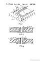
- FIG. 1 is a perspective view of a printed circuit board
- FIG. 2 is an enlarged cutaway section of the circuit board taken along lines 2--2 of FIG. 1 showing the various layers of material on the surface of the board;
- FIG. 3 is a flow chart type of table showing the sequence of processing steps of the present invention.
- FIG. 4 is a cutaway section similar to FIG. 2 but showing the layers of material existing on the surface of the board after processing the board by means of the inventive method shown in FIG. 3.
- FIG. 1 shows a printed wiring board 10 having a substrate member 11 into which are drilled a plurality of thru holes 12 extending between top surface 13 and bottom surface 14 of the substrate.
- Thru holes 12 can serve either of two purposes: they can provide a means for extending an electrical connection from a circuit pattern on the top surface 13 to a circuit pattern located on bottom side 14 of board 10; or they can serve as receptacles and electrical contacts for inserted leads of a component 15 which is to be mounted on the board.
- the walls of thru holes 12 must be placed with a material, typically solder, which exhibits good electrical conductivity.
- circuit patterns including conductor paths 16 constituting parts or all of the shown fine line conductors and adapted for providing electrical connection among various locations on the surfaces.
- a printed wiring board 10 uses a substrate 11, typically made of epoxy coated glass, on which a copper foil layer 21 is affixed to each surface 13 and 14 as seen in FIG. 2.
- a substrate of this type can be purchased from Westinghouse Inc. of Hampton, S.C. as the FR4 copper clad material.
- Substrate 11 is then placed in a drilling machine and thru holes 12 are drilled at precise locations. After deburring drilled holes 12 and cleaning surfaces 13 and 14, circuit path configurations 16 are applied to selected land areas of surfaces 13 and 14 by any well known manufacturing process.
- One such process involves dipping substrate 11 into a bath of ammonium persulfate to partially etch copper foil layer 21 after which the substrate is cleaned by dipping it into sulfuric acid.
- the partially etched and cleaned substrate 11 is then placed in a bath of hydrochloric acid which acts to condition the copper surfaces 21 to accept a coating of tin-palladium when substrate 11 is next dipped into a bath of tin-palladium colloid.
- an accelerator such as fluboric acid to remove the tin from the tin-palladium coating and expose the palladium.
- Substrate 11 with an exposed coating of palladium, is next dipped into an electroless copper bath, typically a solution of sodium hydroxide, copper sulfate, formaldehyde and ethylene diaminetetra acetic acid. (N a OH, C u SO 4 , CHO, and E.D.T.A.), where the palladium acts as a catalyst for accelerating the adherence of copper onto surfaces 13 and 14 of substrate 11.
- an electroless copper bath typically a solution of sodium hydroxide, copper sulfate, formaldehyde and ethylene diaminetetra acetic acid. (N a OH, C u SO 4 , CHO, and E.D.T.A.), where the palladium acts as a catalyst for accelerating the adherence of copper onto surfaces 13 and 14 of substrate 11.
- Surfaces 13 and 14 of substrate 11 are now coated with a layer 22 of copper typically 50 micro inches thick.
- the thickness of copper layer 22 is directly related to the amount of time that substrate 11 is suspended in the electroless copper bath, the more time substrate 11 is immeresed in the bath the thicker layer 22 becomes.
- a laminate dry film of photo-sensitive polymer material is applied to each surface 13, 14 on which copper layer 22 has been applied.
- One of the surfaces, surface 13 of substrate 11 is now exposed to ultra-violet light through a mask, typically a film art master, to delineate catalytic metal deposition sites at the exposed areas.
- the film art master has located on one of its surfaces darkened land areas, or opaque sections, representing the outline of the circuit path configuration which is to be exposed on to the photo-sensitive coated surface 13 by exposure to the ultra-violet light.
- the ultra-violet light causes the positions of the photo sensitive coating which are exposed to become hard; the portions of the photo-sensitive layer which become hard outline the circuit patterns which will remain on board surface 13.
- the above steps are performed on surface 14, that is a photo-sensitive layer is applied to surface 14 and then exposed to ultra-violet light through a mask to delineate circuit path patterns on surface 14.
- surfaces 13 and 14 are simultaneously laminated and simultaneously exposed to ultra-violet light instead of sequentially.
- substrate 11 After exposure of surfaces 13 and 14 to ultra-violet light, substrate 11 is placed in a bath of 1-1-1trichloroethane developer to remove the unexposed, or soft, photo-sensitive polymer. Substrate 11, after washing, is then dipped into a copper electro-plating bath to build a 1 mil inch thick copper trace 22 on the circuit paths 16 and into a solder electro-plating bath to build a 0.3 mil thick coating of solder 23 on the copper trace 22. Substrate 11 is next placed into a bath of solvent, typically methylene chloride, to remove the hardened photo-sensitive layer and then into a bath of alkaline type etchant to etch or remove the unwanted exposed layer of copper foil from surfaces 13 and 14. The coating of solder 23 acts as an etchant resist to prevent the copper traces 22 from being attacked by the etchant.
- solvent typically methylene chloride
- FIG. 2 is an end view of a substrate 11 with the depicted dimensions exaggerated, particularly the thickness of the various layers on substrate 11 and the width of thru hole 12.
- substrate 11 has placed on surfaces 13 and 14 and on wall 24 of thru hole 12 a layer of copper foil 21, a layer of electro-plated copper 22 and a layer of electro-plated solder 23. If components are inserted into thru holes 12 on substrate 11 and substrate 11 is then passed thru a solder wave bath, solder layer 23 becomes sufficiently heated to melt and form a short circuit between adjacent conductor paths 16. To prevent these unwanted short circuits from occurring, substrate 11 is moved through the sequence of processing steps shown in FIG. 3.
- substrate 11 is coated with a photo-polymer resist and a phototool, which is essentially a shield or screen, placed over each of surfaces 13 and 14 (step 32) prior to exposing the surfaces to ultra-violet light (step 33).
- the phototool typically a film art master, has located on one of its surfaces darkened land areas, or opaque sections, which block the passage of light therethrough. Opaque sections are positioned to prevent the photopolymer resist coating, which is covering the solder on the circuit traces, from being exposed to light when the art master is placed over the surface.
- Substrate 11 is exposed to ultra-violet light having a minimum energy of 80 millijoules/CM2 at 365 nanometers or until the exposed coating of photopolymer resist hardens. The ultra-violet light hardens the resist covering the solder in and adjacent to thru holes 12 (FIG. 1) while the resist covering the circuit paths 16 remains soft.
- Substrate 11, having a hardened resist coating 26 over solder traces in and around thru holes 12 and a softened resist coating over circuit traces 16, is now placed in a solvent bath where the solvent is typically 1-1-1trichloroethane as seen in step 34 of FIG. 3.
- the solvent removes the soft resist thereby leaving solder traces 23 on the circuit paths bare.
- substrate 11 is dipped into a bath of solder strip, typically containing fluoride, to remove the solder traces from the circuit paths (step 35). After removal from the solder strip bath, the hardened polymer resist located on and adjacent to the thru holes 12 is removed by washing substrate 11 in a methylene chloride bath as seen in step 36.
- Substrate 11 now has solder traces in and around thru holes 12 with no solder traces covering circuit paths 16 as seen in FIG. 4.
- components can now be placed on printed wiring board 10 and the board moved through a solder wave bath without any short circuits formed between adjacent circuit paths 16 by melted solder since the solder has been removed from the circuit paths and the solder mask prevents new solder from adhering to the paths.
Abstract
Description
Claims (2)
Priority Applications (1)
| Application Number | Priority Date | Filing Date | Title |
|---|---|---|---|
| US06/500,681 US4487828A (en) | 1983-06-03 | 1983-06-03 | Method of manufacturing printed circuit boards |
Applications Claiming Priority (1)
| Application Number | Priority Date | Filing Date | Title |
|---|---|---|---|
| US06/500,681 US4487828A (en) | 1983-06-03 | 1983-06-03 | Method of manufacturing printed circuit boards |
Publications (1)
| Publication Number | Publication Date |
|---|---|
| US4487828A true US4487828A (en) | 1984-12-11 |
Family
ID=23990475
Family Applications (1)
| Application Number | Title | Priority Date | Filing Date |
|---|---|---|---|
| US06/500,681 Expired - Lifetime US4487828A (en) | 1983-06-03 | 1983-06-03 | Method of manufacturing printed circuit boards |
Country Status (1)
| Country | Link |
|---|---|
| US (1) | US4487828A (en) |
Cited By (8)
| Publication number | Priority date | Publication date | Assignee | Title |
|---|---|---|---|---|
| DE3623505A1 (en) * | 1986-07-09 | 1988-01-21 | Deutsche Telephonwerk Kabel | METHOD FOR PRODUCING CIRCUIT BOARDS WITH GALVANIC LEAD-TIN LAYERS SELECTIVELY APPLIED ON THE SOLUTION EYES AND HOLE WALLS |
| EP0361752A2 (en) * | 1988-09-26 | 1990-04-04 | AT&T Corp. | Selective solder formation on printed circuit boards |
| US5545440A (en) * | 1994-12-05 | 1996-08-13 | At&T Global Information Solutions Company (Aka Ncr Corporation) | Method and apparatus for polymer coating of substrates |
| US5863597A (en) * | 1996-01-23 | 1999-01-26 | Sundstrand Corporation | Polyurethane conformal coating process for a printed wiring board |
| US20070130739A1 (en) * | 2004-02-02 | 2007-06-14 | Japan Science And Technology Agency | Method for fabricating piezoelectric element |
| US20080038670A1 (en) * | 2006-08-08 | 2008-02-14 | Endicott Interconnect Technologies, Inc. | Solder mask application process |
| US20150237738A1 (en) * | 2012-09-20 | 2015-08-20 | Jumatech Gmbh | Method for producing a circuit board element, and circuit board element |
| CN110933873A (en) * | 2019-11-25 | 2020-03-27 | 江门市鼎峰照明电子科技有限公司 | Manufacturing method of double-sided circuit board |
Citations (15)
| Publication number | Priority date | Publication date | Assignee | Title |
|---|---|---|---|---|
| US3266125A (en) * | 1962-11-13 | 1966-08-16 | Douglas Aircraft Co Inc | Method for making electrical circuit modules |
| US3565707A (en) * | 1969-03-03 | 1971-02-23 | Fmc Corp | Metal dissolution |
| US3574933A (en) * | 1968-11-29 | 1971-04-13 | Sylvania Electric Prod | Method of making printed circuit boards with plated-through holes |
| US3589004A (en) * | 1968-09-13 | 1971-06-29 | North American Rockwell | Process of making reinforced flat cable terminations |
| US3607474A (en) * | 1968-01-26 | 1971-09-21 | Us Army | Method of making an optical mask for reproducing circuit boards |
| US3677849A (en) * | 1967-05-23 | 1972-07-18 | Pirelli | Medium voltage cables |
| US3778900A (en) * | 1970-09-04 | 1973-12-18 | Ibm | Method for forming interconnections between circuit layers of a multi-layer package |
| GB1396481A (en) * | 1973-02-15 | 1975-06-04 | Matsushita Electric Ind Co Ltd | Manufacture of printed circuit boards |
| DE2614059A1 (en) * | 1976-03-30 | 1977-10-06 | Siemens Ag | Copper-coated printed circuit board prodn. - uses thick tin or tin-lead coating produced by hot tinning on areas to be drilled or punched |
| US4104111A (en) * | 1977-08-03 | 1978-08-01 | Mack Robert L | Process for manufacturing printed circuit boards |
| JPS53142337A (en) * | 1977-05-19 | 1978-12-12 | Fujitsu Ltd | Manufacture of copper through hole plate |
| JPS555877A (en) * | 1978-06-30 | 1980-01-17 | Eidai Kogyo Kk | Device for splintering agalmatolite or like by disc saw |
| US4229879A (en) * | 1977-07-28 | 1980-10-28 | Societe Anonyme De Telecommunications | Manufacture of printed circuit boards |
| US4283480A (en) * | 1978-10-03 | 1981-08-11 | Diamond Shamrock Industrial Chemicals Limited | Photopolymerizable compositions, methods for their preparation, and methods for their use in coating substrates |
| US4325780A (en) * | 1980-09-16 | 1982-04-20 | Schulz Sr Robert M | Method of making a printed circuit board |
-
1983
- 1983-06-03 US US06/500,681 patent/US4487828A/en not_active Expired - Lifetime
Patent Citations (15)
| Publication number | Priority date | Publication date | Assignee | Title |
|---|---|---|---|---|
| US3266125A (en) * | 1962-11-13 | 1966-08-16 | Douglas Aircraft Co Inc | Method for making electrical circuit modules |
| US3677849A (en) * | 1967-05-23 | 1972-07-18 | Pirelli | Medium voltage cables |
| US3607474A (en) * | 1968-01-26 | 1971-09-21 | Us Army | Method of making an optical mask for reproducing circuit boards |
| US3589004A (en) * | 1968-09-13 | 1971-06-29 | North American Rockwell | Process of making reinforced flat cable terminations |
| US3574933A (en) * | 1968-11-29 | 1971-04-13 | Sylvania Electric Prod | Method of making printed circuit boards with plated-through holes |
| US3565707A (en) * | 1969-03-03 | 1971-02-23 | Fmc Corp | Metal dissolution |
| US3778900A (en) * | 1970-09-04 | 1973-12-18 | Ibm | Method for forming interconnections between circuit layers of a multi-layer package |
| GB1396481A (en) * | 1973-02-15 | 1975-06-04 | Matsushita Electric Ind Co Ltd | Manufacture of printed circuit boards |
| DE2614059A1 (en) * | 1976-03-30 | 1977-10-06 | Siemens Ag | Copper-coated printed circuit board prodn. - uses thick tin or tin-lead coating produced by hot tinning on areas to be drilled or punched |
| JPS53142337A (en) * | 1977-05-19 | 1978-12-12 | Fujitsu Ltd | Manufacture of copper through hole plate |
| US4229879A (en) * | 1977-07-28 | 1980-10-28 | Societe Anonyme De Telecommunications | Manufacture of printed circuit boards |
| US4104111A (en) * | 1977-08-03 | 1978-08-01 | Mack Robert L | Process for manufacturing printed circuit boards |
| JPS555877A (en) * | 1978-06-30 | 1980-01-17 | Eidai Kogyo Kk | Device for splintering agalmatolite or like by disc saw |
| US4283480A (en) * | 1978-10-03 | 1981-08-11 | Diamond Shamrock Industrial Chemicals Limited | Photopolymerizable compositions, methods for their preparation, and methods for their use in coating substrates |
| US4325780A (en) * | 1980-09-16 | 1982-04-20 | Schulz Sr Robert M | Method of making a printed circuit board |
Non-Patent Citations (4)
| Title |
|---|
| Huopana, IBM Tech. Disc. Bull., vol. 1, #5, Feb. 1959, p. 36. |
| Huopana, IBM Tech. Disc. Bull., vol. 1, 5, Feb. 1959, p. 36. * |
| Villanuci et al., "Electronic Techniques" Prentice-Hall Inc., Englewood Cliffs, N.J., pp. 283-293. |
| Villanuci et al., Electronic Techniques Prentice Hall Inc., Englewood Cliffs, N.J., pp. 283 293. * |
Cited By (12)
| Publication number | Priority date | Publication date | Assignee | Title |
|---|---|---|---|---|
| DE3623505A1 (en) * | 1986-07-09 | 1988-01-21 | Deutsche Telephonwerk Kabel | METHOD FOR PRODUCING CIRCUIT BOARDS WITH GALVANIC LEAD-TIN LAYERS SELECTIVELY APPLIED ON THE SOLUTION EYES AND HOLE WALLS |
| EP0361752A2 (en) * | 1988-09-26 | 1990-04-04 | AT&T Corp. | Selective solder formation on printed circuit boards |
| EP0361752A3 (en) * | 1988-09-26 | 1990-06-13 | American Telephone And Telegraph Company | Selective solder formation on printed circuit boards |
| US4978423A (en) * | 1988-09-26 | 1990-12-18 | At&T Bell Laboratories | Selective solder formation on printed circuit boards |
| US5545440A (en) * | 1994-12-05 | 1996-08-13 | At&T Global Information Solutions Company (Aka Ncr Corporation) | Method and apparatus for polymer coating of substrates |
| US5863597A (en) * | 1996-01-23 | 1999-01-26 | Sundstrand Corporation | Polyurethane conformal coating process for a printed wiring board |
| US20070130739A1 (en) * | 2004-02-02 | 2007-06-14 | Japan Science And Technology Agency | Method for fabricating piezoelectric element |
| US7770273B2 (en) * | 2004-02-02 | 2010-08-10 | Japan Science And Technology Agency | Method for fabricating piezoelectric element |
| US20080038670A1 (en) * | 2006-08-08 | 2008-02-14 | Endicott Interconnect Technologies, Inc. | Solder mask application process |
| US8288266B2 (en) | 2006-08-08 | 2012-10-16 | Endicott Interconnect Technologies, Inc. | Circuitized substrate assembly |
| US20150237738A1 (en) * | 2012-09-20 | 2015-08-20 | Jumatech Gmbh | Method for producing a circuit board element, and circuit board element |
| CN110933873A (en) * | 2019-11-25 | 2020-03-27 | 江门市鼎峰照明电子科技有限公司 | Manufacturing method of double-sided circuit board |
Similar Documents
| Publication | Publication Date | Title |
|---|---|---|
| US4528259A (en) | Printed wiring boards with solder mask over bare copper wires having large area thickened circuit pad connections | |
| US4720324A (en) | Process for manufacturing printed circuit boards | |
| US4775611A (en) | Additive printed circuit boards with flat surface and indented primary wiring conductors | |
| CA2067710A1 (en) | Process for manufacturing printed circuits employing selective provision of solderable coating | |
| US5985521A (en) | Method for forming electrically conductive layers on chip carrier substrates having through holes or via holes | |
| US4487828A (en) | Method of manufacturing printed circuit boards | |
| US3483615A (en) | Printed circuit boards | |
| EP0784914B1 (en) | Method of manufacturing a printed circuit board | |
| JPH04186792A (en) | Printed wiring board and manufacture thereof | |
| US5905018A (en) | Method of preparing a substrate surface for conformal plating | |
| US6020049A (en) | Product for producing viaholes in reinforced laminates and the related method for manufacturing viaholes | |
| JPH07142841A (en) | Manufacture of printed wiring board | |
| KR101170753B1 (en) | Method of manufacturing flexible printed circuit board | |
| JPH036880A (en) | Printed wiring board and manufacture thereof | |
| JP3395222B2 (en) | Manufacturing method of printed wiring board | |
| JPH08107263A (en) | Manufacturing method of printed-wiring board | |
| CA1258138A (en) | Method for manufacture of printed circuit boards having solder-masked traces | |
| JPS6012791A (en) | Method of producing printed circuit board | |
| JPH0786727A (en) | Printed-wiring board and manufacture thereof | |
| JP2712997B2 (en) | Solder resist processing method in manufacturing printed wiring board | |
| JP2699757B2 (en) | Manufacturing method of printed wiring board | |
| KR20030042873A (en) | The method for manufacturing circuit pattern of printed circuit board using resist plating by pure metal | |
| CN115643681A (en) | Circuit board and manufacturing method thereof | |
| JPS6369290A (en) | Manufacture of printed wiring board | |
| KR910007475B1 (en) | Multi - printed circuit board method |
Legal Events
| Date | Code | Title | Description |
|---|---|---|---|
| AS | Assignment |
Owner name: WESTERN ELECTRIC COMPANY, INCORPORATED 222 BROADWA Free format text: ASSIGNMENT OF ASSIGNORS INTEREST.;ASSIGNORS:HLADOVCAK, RAYMOND C.;KEATING, WALTER W.;REEL/FRAME:004136/0311 Effective date: 19830527 |
|
| AS | Assignment |
Owner name: AT & T TECHNOLOGIES, INC., Free format text: CHANGE OF NAME;ASSIGNOR:WESTERN ELECTRIC COMPANY, INCORPORATED;REEL/FRAME:004251/0868 Effective date: 19831229 |
|
| STCF | Information on status: patent grant |
Free format text: PATENTED CASE |
|
| FEPP | Fee payment procedure |
Free format text: PAYOR NUMBER ASSIGNED (ORIGINAL EVENT CODE: ASPN); ENTITY STATUS OF PATENT OWNER: LARGE ENTITY |
|
| FPAY | Fee payment |
Year of fee payment: 4 |
|
| FPAY | Fee payment |
Year of fee payment: 8 |
|
| FPAY | Fee payment |
Year of fee payment: 12 |