US4409496A - MOS Device including a substrate bias generating circuit - Google Patents
MOS Device including a substrate bias generating circuit Download PDFInfo
- Publication number
- US4409496A US4409496A US06/232,032 US23203281A US4409496A US 4409496 A US4409496 A US 4409496A US 23203281 A US23203281 A US 23203281A US 4409496 A US4409496 A US 4409496A
- Authority
- US
- United States
- Prior art keywords
- substrate
- potential
- circuit
- pumping
- clock signals
- Prior art date
- Legal status (The legal status is an assumption and is not a legal conclusion. Google has not performed a legal analysis and makes no representation as to the accuracy of the status listed.)
- Expired - Fee Related
Links
Images


Classifications
-
- G—PHYSICS
- G11—INFORMATION STORAGE
- G11C—STATIC STORES
- G11C11/00—Digital stores characterised by the use of particular electric or magnetic storage elements; Storage elements therefor
- G11C11/21—Digital stores characterised by the use of particular electric or magnetic storage elements; Storage elements therefor using electric elements
- G11C11/34—Digital stores characterised by the use of particular electric or magnetic storage elements; Storage elements therefor using electric elements using semiconductor devices
- G11C11/40—Digital stores characterised by the use of particular electric or magnetic storage elements; Storage elements therefor using electric elements using semiconductor devices using transistors
- G11C11/401—Digital stores characterised by the use of particular electric or magnetic storage elements; Storage elements therefor using electric elements using semiconductor devices using transistors forming cells needing refreshing or charge regeneration, i.e. dynamic cells
- G11C11/403—Digital stores characterised by the use of particular electric or magnetic storage elements; Storage elements therefor using electric elements using semiconductor devices using transistors forming cells needing refreshing or charge regeneration, i.e. dynamic cells with charge regeneration common to a multiplicity of memory cells, i.e. external refresh
- G11C11/404—Digital stores characterised by the use of particular electric or magnetic storage elements; Storage elements therefor using electric elements using semiconductor devices using transistors forming cells needing refreshing or charge regeneration, i.e. dynamic cells with charge regeneration common to a multiplicity of memory cells, i.e. external refresh with one charge-transfer gate, e.g. MOS transistor, per cell
-
- G—PHYSICS
- G05—CONTROLLING; REGULATING
- G05F—SYSTEMS FOR REGULATING ELECTRIC OR MAGNETIC VARIABLES
- G05F3/00—Non-retroactive systems for regulating electric variables by using an uncontrolled element, or an uncontrolled combination of elements, such element or such combination having self-regulating properties
- G05F3/02—Regulating voltage or current
- G05F3/08—Regulating voltage or current wherein the variable is dc
- G05F3/10—Regulating voltage or current wherein the variable is dc using uncontrolled devices with non-linear characteristics
- G05F3/16—Regulating voltage or current wherein the variable is dc using uncontrolled devices with non-linear characteristics being semiconductor devices
- G05F3/20—Regulating voltage or current wherein the variable is dc using uncontrolled devices with non-linear characteristics being semiconductor devices using diode- transistor combinations
- G05F3/205—Substrate bias-voltage generators
-
- G—PHYSICS
- G11—INFORMATION STORAGE
- G11C—STATIC STORES
- G11C11/00—Digital stores characterised by the use of particular electric or magnetic storage elements; Storage elements therefor
- G11C11/21—Digital stores characterised by the use of particular electric or magnetic storage elements; Storage elements therefor using electric elements
- G11C11/34—Digital stores characterised by the use of particular electric or magnetic storage elements; Storage elements therefor using electric elements using semiconductor devices
- G11C11/40—Digital stores characterised by the use of particular electric or magnetic storage elements; Storage elements therefor using electric elements using semiconductor devices using transistors
- G11C11/401—Digital stores characterised by the use of particular electric or magnetic storage elements; Storage elements therefor using electric elements using semiconductor devices using transistors forming cells needing refreshing or charge regeneration, i.e. dynamic cells
- G11C11/4063—Auxiliary circuits, e.g. for addressing, decoding, driving, writing, sensing or timing
- G11C11/407—Auxiliary circuits, e.g. for addressing, decoding, driving, writing, sensing or timing for memory cells of the field-effect type
- G11C11/4074—Power supply or voltage generation circuits, e.g. bias voltage generators, substrate voltage generators, back-up power, power control circuits
-
- H—ELECTRICITY
- H01—ELECTRIC ELEMENTS
- H01L—SEMICONDUCTOR DEVICES NOT COVERED BY CLASS H10
- H01L27/00—Devices consisting of a plurality of semiconductor or other solid-state components formed in or on a common substrate
- H01L27/02—Devices consisting of a plurality of semiconductor or other solid-state components formed in or on a common substrate including semiconductor components specially adapted for rectifying, oscillating, amplifying or switching and having at least one potential-jump barrier or surface barrier; including integrated passive circuit elements with at least one potential-jump barrier or surface barrier
- H01L27/0203—Particular design considerations for integrated circuits
- H01L27/0214—Particular design considerations for integrated circuits for internal polarisation, e.g. I2L
- H01L27/0218—Particular design considerations for integrated circuits for internal polarisation, e.g. I2L of field effect structures
- H01L27/0222—Charge pumping, substrate bias generation structures
Definitions
- the present invention relates to an MOS integrated circuit and, more particularly, to an MOS device including a substrate bias generating circuit formed in a chip.
- a negative bias voltage is applied to the substrate thereof, in order to suppress a source-substrate effect which affects threshold voltage and, in addition, in order to increase the operation speed of the device by decreasing junction capacitances between the substrate and each of the diffusion layers.
- one external power supply for the negative bias voltage is usually necessary.
- a substrate bias generating circuit which is formed in a chip has been provided (Ref. U.S. Pat. No. 3,806,741). An MOS device having such a substrate bias generating circuit therein does not require the above-mentioned external power supply.
- the substrate bias generating circuit comprises a pumping circuit for absorbing such positive charges in the substrate.
- the potential of the substrate remains lower than a predetermined value. It should be noted that variation of the substrate potential occurs more or less in association with the operation of internal circuits, such as memory cells, decoders or the like.
- the pumping operation by the pumping circuit is not in synchronization with the operation of the internal circuits.
- the pumping operation may be effected when the substrate potential is low.
- the efficiency of pumping is low, since the difference between the substrate potential and the lowest potential of the pumping circuit is small.
- the pumping operation by the pumping circuit is independent from the magnitude of the potential of the substrate, even when the pumping operation is in synchronization with the operation of the internal circuits.
- the pumping operation may also be effected when the substrate potential is low. In any case, the efficiency of pumping is low and, accordingly, the average level of the substrate potential is relatively high, which invites incomplete isolation between elements, unstable threshold voltages and a low operation speed.
- an MOS device including a substrate bias circuit, comprising: a clock generator for receiving an external clock signal and generating first and second internal clock signals; an internal circuit, connected to the clock generator, which is operated by the internal clock signals; a pumping circuit driver, connected to the clock generator, for receiving the internal clock signals and generating third and fourth internal clock signals which are in synchronization with the internal clock signals and are in opposite phase with each other; and, a pumping circuit, connected to the pumping circuit driver and driven by the third and fourth internal clock signals, for generating a substrate potential, the pumping operation of the pumping circuit being effected when the substrate potential is relatively high.
- the pumping efficiency is high; in other words, the quantity of charges flowing from the substrate to the pumping circuit is large since the pumping operation is effected when the substrate potential is high. Accordingly, the average level of the substrate potential can be decreased compared with those of the prior art.
- FIG. 1 is a circuit diagram illustrating a memory cell portion including a sense amplifier of an MOS dynamic memory, for explaining a variation of a substrate potential;
- FIG. 2 is a circuit diagram illustrating a decoder portion of the MOS dynamic memory, for explaining another variation of the substrate potential
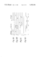
- FIGS. 3A through 3D are timing diagrams showing the signals appearing in the circuits of FIGS. 1 and 2;
- FIG. 4 is a block diagram illustrating an embodiment of the MOS device including a substrate bias generating circuit according to the present invention
- FIG. 5 is a circuit diagram of the pumping circuit driver 43 of FIG. 4;
- FIG. 6 is a circuit diagram of the pumping circuit 44 of FIG. 4, and;
- FIGS. 7A through 7D are timing diagrams showing the signals appearing in the circuits of FIGS. 4 and 6.
- each of the memory cells MC 0 , MC 1 , . . . , MC i , MC i+1 , MC i+2 , . . . , MC n which is of a one-transistor type, comprises a transistor Q and a capacitor C.
- dummy cells DC 1 and DC 2 are provided. Since the charge stored in the capacitor C is distributed to floating capacitances of bit lines BL, and BL the resulting difference in potential between the bit lines BL and BL are very small.
- the potential of a clock ⁇ 0 is high, so that the bit lines BL and BL are precharged, while, during a reading operation time, the potential of the clock ⁇ 1 is high, so that data is introduced from a selected memory cell to the bit lines BL and BL and, after that, the data is read out by a sense amplifier SA.
- FIGS. 3A through 3C the operation of the circuit of FIG. 1 is explained. It is assumed that the content stored in the memory cell MC 0 is read out in synchronization with an external clock signal EXC, as shown in FIG. 3A.
- the potential of the internal clock signal ⁇ 0 becomes low and, simultaneously, the potentials of a word line W 0 and a dummy word line DW 1 become high.
- the transistor Q of the memory cell MC 0 turns on so that the capacitor C is connected to the bit line BL, while a transistor Q D1 of the dummy cell DC 1 turns on so that the capacitor C D is connected to the bit lines BL.
- the transistors Q S1 and Q S2 are conductive and non-conductive, respectively.
- the charge in the bit line BL flows through the transistor Q S1 so that the potential of the bit line BL becomes lower. Therefore, as illustrated in FIG. 3C, the difference in potential between the bit lines BL and BL becomes larger. This difference is detected by a read amplifier (not shown) which means that the read operation for the content in the memory cell MC 0 is completed.
- the potentials of the word line W 0 and the dummy word line W D1 becomes low again and, accordingly, the bit lines BL and BL are again precharged.
- Such changes of the potentials of the bit lines invite a variation of a substrate potential, since the bit lines are usually formed by diffusion layers in the substrate, and junction capacitances between the diffusion layers and the substrate are large.
- FIG. 2 is also a circuit diagram illustrating a decoder portion of the MOS dynamic memory and used for explaining a variation of the substrate potential.
- word lines W 0 , W 1 , . . . , W n are the same as those of FIG. 1.
- ⁇ W indicates a power supply for the decoders.
- the selection of the word lines W 0 , W 1 , . . . , W n is carried out by address signals A 0 , A 1 , . . . , A m and their inverted signals A 0 , A 1 , . . . , A m .
- a decoder DEC 0 if all the potentials of the address signals A 0 , A 1 , . . . , A m are low, the transistors Q 10 , Q 11 , . . . , Q 1m are non-conductive, so that the potential of a signal line L remains high. Therefore, the transistor Q 20 is conductive, so that the potential of the word line W 0 is high, which means that a word line W 0 is selected. Contrary to this, if the potential of at least one of the address signals A 0 , A 1 , . . . , A m is high, the corresponding transistors Q 10 , Q 11 , . . .
- Q 1m conduct so that the potential of the signal line L becomes low. Therefore, the transistor Q 20 is non-conductive so that the potential of the word line W 0 is low, which means that the word line W 0 is non-selected.
- the signal line L is precharged by the internal clock signal ⁇ 0 , as illustrated in FIG. 3B. For the non-selected state, the potential of the signal line L becomes low and, after that, the signal line L is again precharged by the high potential of the clock signal ⁇ 0 .
- Such a change of the potential of the signal line L also invites a variation of the substrate potential, since the signal line L is usually formed by a diffusion layer in the substrate, and the junction capacitance between the diffusion layer and the substrate is large.
- the substrate potential V BB is changed, as illustrated in FIG. 3D.
- the variation ⁇ V BB of the substrate potential V BB is 1 or 2 volts.
- the substrate potential V BB There is no problem when the substrate potential V BB is low, but there are various problems when the substrate potential V BB is high. Firstly, the p-n junction between the substrate and source or drain region is forward biased and, accordingly, isolation between the substrate and each of the elements is incomplete. Secondly, the circuit operation becomes unstable when the substrate potential V BB approaches zero, since the variation of a threshold voltage is inversely proportional to a value ⁇
- the pumping operation by the substrate bias generating circuit which absorbs positive charges from the substrate, is not in synchronization with the operation of internal circuits, such as memory cells or decoders.
- the substrate potential V BB is altered responsive to a ratio between the periods A and B, as illustrated in FIG. 3D.
- the pumping operation is in synchronization with the operation of the internal circuits and, in addition, the pumping operation is always carried out during the period A.
- FIG. 4 is a block diagram illustrating an embodiment of the MOS device including a substrate bias generating circuit according to the present invention.
- a clock generator 41 receives an external clock signal EXC as shown in FIG. 7A and generates first and second internal clock signals ⁇ 0 and ⁇ 1 , as shown in FIG. 7B, to the internal circuit 42 and the pumping circuit driver 43.
- the pumping circuit driver 43 delays the internal clock signals ⁇ 0 and ⁇ 1 for a predetermined time and generates third and fourth internal clock signals ⁇ A and ⁇ B , as shown in FIG.
- the internal clock signals ⁇ A and ⁇ B are in synchronization with the rising of the internal clock signals ⁇ 1 and ⁇ 0 , respectively.
- the time delay caused by the pumping circuit driver 43 is determined to be a value which insures that the pumping operation of the pumping circuit 44 is carried out when the substrate potential V BB is high.
- FIG. 5 is a circuit diagram of the pumping circuit driver 43 of FIG. 4.
- the pumping circuit driver 43 comprises a portion 43A for generating the clock signal ⁇ A and a portion 43B for generating the clock ⁇ B signal. Both comprise the same components.
- Each of the parts 43A and 43B comprises five pairs of series-connected transistors Q 31 and Q 32 , Q 33 and Q 34 , Q 36 and Q 37 , Q 38 and Q 39 , and Q 40 and Q 41 , a transistor Q 35 connected between the node P 2 and the gate of the transistor Q 36 , and a capacitor C 5 connected between the gate and the source of the transistor Q 38 .
- the transistor Q 34 serves as an element for determining the delay time of the pumping circuit driver 43.
- the transistors Q 32 , Q 33 , Q.sub. 36 and Q 37 are conductive, while the transistor Q 31 is non-conductive. Therefore, the potential at the node P 1 becomes low and the transistor Q 34 turns off so that the potential at the node P 2 becomes high. Therefore, the transistors Q 39 and Q 41 are conductive.
- the transistor Q 36 is conductive and the potential of the clock signal ⁇ 1 is low, the potential at the node P 3 remains low and, accordingly, the transistors Q 38 and Q 40 are non-condutive. As a result, the potentials at the nodes P 4 and P 5 are low and, accordingly, the potential of the clock signal ⁇ A is low. Contrary to this, in the generating portion 43B, the potential of the clock signal ⁇ B is high.
- the potentials of the clock signals ⁇ 0 and ⁇ 1 are low and high, respectively, the potentials of the clock signals ⁇ A and ⁇ B are high and low, respectively. It should be noted that, when both of the potentials of the clock signals ⁇ 0 and ⁇ 1 are low, the potentials of the clock signals ⁇ A and ⁇ B remain responsive to previous states of the clock signals ⁇ 0 and ⁇ 1 . Therefore, the clock signals ⁇ A and ⁇ B are in synchronization with the rising of the clock signal ⁇ 1 and ⁇ 0 , respectively (which are not always in opposite phase with each other), and are in opposite phase with each other.
- FIG. 6 is a circuit diagram of the pumping circuit 44 of FIG. 4.
- a transistor Q 61 a diode D 6 and a capacitor C 6 serves as a pump for absorbing positive charges from the substrate.
- Transistors Q 62 through Q 65 are switching elements for charging the capacitor C 6 and operating the above-mentioned pump. Referring to FIG. 7D, the operation of the circuit of FIG. 6 is explained.
- the transistors Q 62 and Q 63 are conductive and, accordingly, the transistor Q 64 which receives the high potential at the node N 3 is conductive.
- the transistors Q 65 and Q 66 are non-conductive.
- the potential at the node N 1 approaches zero, while the potential at the node N 2 approaches a power supply voltage V CC , so that the capacitor C 6 is charged.
- the substrate potential V BB remains negative, no current flows from the substrate to the node N 1 .
- the MOS device including a substrate bias generating circuit according to the present invention has such an advantage, as compared with those of the prior art, that the average level of the substrate potential can be decreased, because, when the substrate potential is high, currents flow from the substrate to the substrate bias generating circuit (the pumping circuit).
Abstract
An MOS device including a substrate bias generating circuit, comprising: a clock generator for receiving an external clock signal and generating first and second internal clock signals; an internal circuit operated by the first and second internal clock signals; a pumping circuit driver for generating third and fourth internal clock signals in synchronization with the first and second internal clock signals and; a pumping circuit operated by the third and fourth internal clock signals. In this device, when the substrate potential (VBB) is relatively high, currents flow from the substrate to the pumping circuit.
Description
1. Technical Field
The present invention relates to an MOS integrated circuit and, more particularly, to an MOS device including a substrate bias generating circuit formed in a chip.
2. Background Art
Generally, in an n-type MOS device, a negative bias voltage is applied to the substrate thereof, in order to suppress a source-substrate effect which affects threshold voltage and, in addition, in order to increase the operation speed of the device by decreasing junction capacitances between the substrate and each of the diffusion layers. For this purpose, one external power supply for the negative bias voltage is usually necessary. However, in recent years, a substrate bias generating circuit which is formed in a chip has been provided (Ref. U.S. Pat. No. 3,806,741). An MOS device having such a substrate bias generating circuit therein does not require the above-mentioned external power supply.
Usually, positive charges are generated in the substrate due to leakage currents through the p-n junctions between the substrate and each of the diffusion layers and due to impact ionization. The substrate bias generating circuit comprises a pumping circuit for absorbing such positive charges in the substrate. Thus, the potential of the substrate remains lower than a predetermined value. It should be noted that variation of the substrate potential occurs more or less in association with the operation of internal circuits, such as memory cells, decoders or the like.
However, in one prior art MOS device which includes a substrate bias generating circuit, the pumping operation by the pumping circuit is not in synchronization with the operation of the internal circuits. In this device, the pumping operation may be effected when the substrate potential is low. As a result, the efficiency of pumping is low, since the difference between the substrate potential and the lowest potential of the pumping circuit is small. In another prior art device, the pumping operation by the pumping circuit is independent from the magnitude of the potential of the substrate, even when the pumping operation is in synchronization with the operation of the internal circuits. In this device, the pumping operation may also be effected when the substrate potential is low. In any case, the efficiency of pumping is low and, accordingly, the average level of the substrate potential is relatively high, which invites incomplete isolation between elements, unstable threshold voltages and a low operation speed.
It is an object of the present invention to provide an MOS device including a substrate bias generating circuit with a low average level of the substrate potential.
Accordingly to the present invention, there is provided an MOS device including a substrate bias circuit, comprising: a clock generator for receiving an external clock signal and generating first and second internal clock signals; an internal circuit, connected to the clock generator, which is operated by the internal clock signals; a pumping circuit driver, connected to the clock generator, for receiving the internal clock signals and generating third and fourth internal clock signals which are in synchronization with the internal clock signals and are in opposite phase with each other; and, a pumping circuit, connected to the pumping circuit driver and driven by the third and fourth internal clock signals, for generating a substrate potential, the pumping operation of the pumping circuit being effected when the substrate potential is relatively high. In this device, the pumping efficiency is high; in other words, the quantity of charges flowing from the substrate to the pumping circuit is large since the pumping operation is effected when the substrate potential is high. Accordingly, the average level of the substrate potential can be decreased compared with those of the prior art.
The present invention will be more clearly understood from the description as set forth below with reference to the accompanying drawings.
FIG. 1 is a circuit diagram illustrating a memory cell portion including a sense amplifier of an MOS dynamic memory, for explaining a variation of a substrate potential;
FIG. 2 is a circuit diagram illustrating a decoder portion of the MOS dynamic memory, for explaining another variation of the substrate potential;
FIGS. 3A through 3D are timing diagrams showing the signals appearing in the circuits of FIGS. 1 and 2;
FIG. 4 is a block diagram illustrating an embodiment of the MOS device including a substrate bias generating circuit according to the present invention;
FIG. 5 is a circuit diagram of the pumping circuit driver 43 of FIG. 4;
FIG. 6 is a circuit diagram of the pumping circuit 44 of FIG. 4, and;
FIGS. 7A through 7D are timing diagrams showing the signals appearing in the circuits of FIGS. 4 and 6.
Referring to FIG. 1, which illustrates a memory cell portion, including a sense amplifier, of an MOS dynamic memory, each of the memory cells MC0, MC1, . . . , MCi, MCi+1, MCi+2, . . . , MCn, which is of a one-transistor type, comprises a transistor Q and a capacitor C. In addition, dummy cells DC1 and DC2 are provided. Since the charge stored in the capacitor C is distributed to floating capacitances of bit lines BL, and BL the resulting difference in potential between the bit lines BL and BL are very small. During standby time, the potential of a clock φ0 is high, so that the bit lines BL and BL are precharged, while, during a reading operation time, the potential of the clock φ1 is high, so that data is introduced from a selected memory cell to the bit lines BL and BL and, after that, the data is read out by a sense amplifier SA.
Referring to FIGS. 3A through 3C, the operation of the circuit of FIG. 1 is explained. It is assumed that the content stored in the memory cell MC0 is read out in synchronization with an external clock signal EXC, as shown in FIG. 3A. In this case, as illustrated in FIG. 3B, the potential of the internal clock signal φ0 becomes low and, simultaneously, the potentials of a word line W0 and a dummy word line DW1 become high. As a result, the transistor Q of the memory cell MC0 turns on so that the capacitor C is connected to the bit line BL, while a transistor QD1 of the dummy cell DC1 turns on so that the capacitor CD is connected to the bit lines BL. Therefore, if the charge stored in the capacitor C of the memory cell MC0 is zero, the potential of the bit line BL becomes low, as illustrated in FIG. 3C. In the sense amplifier SA, the transistors QS1 and QS2 are conductive and non-conductive, respectively. As a result, the charge in the bit line BL flows through the transistor QS1 so that the potential of the bit line BL becomes lower. Therefore, as illustrated in FIG. 3C, the difference in potential between the bit lines BL and BL becomes larger. This difference is detected by a read amplifier (not shown) which means that the read operation for the content in the memory cell MC0 is completed. After that, the potentials of the word line W0 and the dummy word line WD1 becomes low again and, accordingly, the bit lines BL and BL are again precharged. Such changes of the potentials of the bit lines invite a variation of a substrate potential, since the bit lines are usually formed by diffusion layers in the substrate, and junction capacitances between the diffusion layers and the substrate are large.
FIG. 2 is also a circuit diagram illustrating a decoder portion of the MOS dynamic memory and used for explaining a variation of the substrate potential. In FIG. 2, word lines W0, W1, . . . , Wn are the same as those of FIG. 1. φW indicates a power supply for the decoders. The selection of the word lines W0, W1, . . . , Wn is carried out by address signals A0, A1, . . . , Am and their inverted signals A0, A1, . . . , Am. For example, in a decoder DEC0, if all the potentials of the address signals A0, A1, . . . , Am are low, the transistors Q10, Q11, . . . , Q1m are non-conductive, so that the potential of a signal line L remains high. Therefore, the transistor Q20 is conductive, so that the potential of the word line W0 is high, which means that a word line W0 is selected. Contrary to this, if the potential of at least one of the address signals A0, A1, . . . , Am is high, the corresponding transistors Q10, Q11, . . . , Q1m conduct so that the potential of the signal line L becomes low. Therefore, the transistor Q20 is non-conductive so that the potential of the word line W0 is low, which means that the word line W0 is non-selected. In such decoders DEC0 , DEC1, . . . , DECn, the signal line L is precharged by the internal clock signal φ0, as illustrated in FIG. 3B. For the non-selected state, the potential of the signal line L becomes low and, after that, the signal line L is again precharged by the high potential of the clock signal φ0. Such a change of the potential of the signal line L also invites a variation of the substrate potential, since the signal line L is usually formed by a diffusion layer in the substrate, and the junction capacitance between the diffusion layer and the substrate is large.
In the MOS dynamic memory, as explained above, changes of the junction capacitances between the substrate and the diffusion layers forming the bit lines BL, BL and, the signal lines L are generated and, similarly, changes of the junction capacitances between the substrate and source or drain diffusion layers are generated. As a result, the substrate potential VBB is changed, as illustrated in FIG. 3D. For example, in a 64K bit dynamic memory using a 5 volt power supply, the variation ΔVBB of the substrate potential VBB is 1 or 2 volts.
There is no problem when the substrate potential VBB is low, but there are various problems when the substrate potential VBB is high. Firstly, the p-n junction between the substrate and source or drain region is forward biased and, accordingly, isolation between the substrate and each of the elements is incomplete. Secondly, the circuit operation becomes unstable when the substrate potential VBB approaches zero, since the variation of a threshold voltage is inversely proportional to a value √|VBB |. Thirdly, when the substrate potential VBB becomes high, junction capacitances between the substrate and each of the diffusion layers also become large, so that the circuit operation becomes slow and unstable.
On the other hand, in the prior art, the pumping operation by the substrate bias generating circuit, which absorbs positive charges from the substrate, is not in synchronization with the operation of internal circuits, such as memory cells or decoders. In this case, the substrate potential VBB is altered responsive to a ratio between the periods A and B, as illustrated in FIG. 3D. For example, if the period B is much longer than the period A, most of the pumping operations may be carried out during the period B, which invites a high average level of the substrate potential VBB. In addition, even when the pumping operation is in synchronization with the operation of the internal circuits, it is of no use that the pumping operation is carried out during the period B. Contrary to this, in the present invention, the pumping operation is in synchronization with the operation of the internal circuits and, in addition, the pumping operation is always carried out during the period A.
FIG. 4 is a block diagram illustrating an embodiment of the MOS device including a substrate bias generating circuit according to the present invention. In FIG. 4, a clock generator 41, an internal circuit 42 such as memory cells or decoders, a pumping circuit driver 43 and a pumping circuit 44 are formed in a chip. The clock generator 41 receives an external clock signal EXC as shown in FIG. 7A and generates first and second internal clock signals φ0 and φ1, as shown in FIG. 7B, to the internal circuit 42 and the pumping circuit driver 43. The pumping circuit driver 43 delays the internal clock signals φ0 and φ1 for a predetermined time and generates third and fourth internal clock signals φA and φB, as shown in FIG. 7C, which are in opposite phase with each other, and are input to the pumping circuit 44. Therefore, the internal clock signals φA and φB are in synchronization with the rising of the internal clock signals φ1 and φ0, respectively. In addition, the time delay caused by the pumping circuit driver 43 is determined to be a value which insures that the pumping operation of the pumping circuit 44 is carried out when the substrate potential VBB is high.
FIG. 5 is a circuit diagram of the pumping circuit driver 43 of FIG. 4. The pumping circuit driver 43 comprises a portion 43A for generating the clock signal φA and a portion 43B for generating the clock φB signal. Both comprise the same components. Each of the parts 43A and 43B comprises five pairs of series-connected transistors Q31 and Q32, Q33 and Q34, Q36 and Q37, Q38 and Q39, and Q40 and Q41, a transistor Q35 connected between the node P2 and the gate of the transistor Q36, and a capacitor C5 connected between the gate and the source of the transistor Q38. Here, the transistor Q34 serves as an element for determining the delay time of the pumping circuit driver 43. For example, in the generating portion 43A, when the potentials of the clock signals φ0 and φ1 are high and low, respectively, the transistors Q32, Q33, Q.sub. 36 and Q37 are conductive, while the transistor Q31 is non-conductive. Therefore, the potential at the node P1 becomes low and the transistor Q34 turns off so that the potential at the node P2 becomes high. Therefore, the transistors Q39 and Q41 are conductive. On the other hand, since the transistor Q36 is conductive and the potential of the clock signal φ1 is low, the potential at the node P3 remains low and, accordingly, the transistors Q38 and Q40 are non-condutive. As a result, the potentials at the nodes P4 and P5 are low and, accordingly, the potential of the clock signal φA is low. Contrary to this, in the generating portion 43B, the potential of the clock signal φB is high.
Similarly, when the potentials of the clock signals φ0 and φ1 are low and high, respectively, the potentials of the clock signals φA and φB are high and low, respectively. It should be noted that, when both of the potentials of the clock signals φ0 and φ1 are low, the potentials of the clock signals φA and φB remain responsive to previous states of the clock signals φ0 and φ1. Therefore, the clock signals φA and φB are in synchronization with the rising of the clock signal φ1 and φ0, respectively (which are not always in opposite phase with each other), and are in opposite phase with each other.
FIG. 6 is a circuit diagram of the pumping circuit 44 of FIG. 4. In FIG. 6, a transistor Q61, a diode D6 and a capacitor C6 serves as a pump for absorbing positive charges from the substrate. Transistors Q62 through Q65 are switching elements for charging the capacitor C6 and operating the above-mentioned pump. Referring to FIG. 7D, the operation of the circuit of FIG. 6 is explained. When the potentials of the clock signals φA and φB are high and low, respectively, the transistors Q62 and Q63 are conductive and, accordingly, the transistor Q64 which receives the high potential at the node N3 is conductive. In addition, the transistors Q65 and Q66 are non-conductive. Therefore, the potential at the node N1 approaches zero, while the potential at the node N2 approaches a power supply voltage VCC, so that the capacitor C6 is charged. In this case, since the substrate potential VBB remains negative, no current flows from the substrate to the node N1.
Next, when the potentials of the clock signals φA and φB are changed to low and high, respectively, the transistors Q62 and Q63 turn off and the transistors Q65 and Q66 conduct. As a result, the potential at the node N3 becomes the same as that at the node N1 and the transistor Q64 turns off. Therefore, the potential at the node N2 approaches zero. Since the transistor Q64 is non-conductive, the potential at the node N1 becomes a negative value. As a result, when the potential at the node N1 becomes lower than the substrate potential VBB, currents flow from the substrate to the node N1 so that the substrate potential VBB is decreased. In the present invention, when the substrate potential VBB becomes high due to noise associated with the operation of the internal circuit, as illustrated by an arrow X in FIG. 7D, currents begin to flow from the substrate to the node N1.
In FIG. 7D, if the substrate potential VBB remains low at the time indicated by the arrow X, the substrate potential VBB is lower than the potential at the node N1 so that no pumping operation is carried out. However, in the present invention, such a phenomenon can rarely happen. Therefore, the efficiency of the pumping operation according to the present invention is high. As explained hereinbefore, the MOS device including a substrate bias generating circuit according to the present invention has such an advantage, as compared with those of the prior art, that the average level of the substrate potential can be decreased, because, when the substrate potential is high, currents flow from the substrate to the substrate bias generating circuit (the pumping circuit).
Claims (6)
1. An MOS device including a substrate bias circuit for controlling the potential on a substrate containing said MOS device, comprising:
a clock generator for receiving an external clock signal and generating first and second internal clock signals;
a circuit internal to said MOS device connected to said clock generator and operated by said first and second internal clock signals;
a pumping circuit driver, connected to said clock generator, for receiving said first and second internal clock signals and generating third and fourth internal clock signals which are in synchronization with said first and second internal clock signals and are in opposite phase with each other; and
a pumping circuit connected to said pumping circuit driver and said substrate and driven by said third and fourth internal clock signals, for generating a potential for biasing said substrate when said pumping circuit effectuates a pumping operation, said pumping circuit effecting said pumping operation when the potential on said substrate is higher than a predetermined value.
2. A device as set forth in claim 1, wherein said internal circuit is a memory cell array including a sense amplifier.
3. A device as set forth in claim 1, wherein said internal circuit is a decoder circuit.
4. A device as set forth in claim 1, wherein said pumping circuit comprises:
a transistor having first, second and third terminals, said first and second terminals connected to said substrate of said MOS device;
a diode operatively connected to said first and third terminals of said transistor;
a capacitor having a first terminal operatively connected to said diode and the third terminal of said transistor to form a node and having a second terminal, said transistor, said diode and said capacitor serving as a pump for absorbing positive charges in said substrate; and
a plurality of switching transistors operatively connected to said pumping circuit driver and said second terminal of said capacitor for receiving said third and fourth internal clock signals and actuating said pump.
5. A device as set forth in claim 4, wherein said pump operates only when the potential at said node is less than the potential on said substrate.
6. A device as set forth in claim 1, 2, 3 or 4, wherein said pumping circuit operates only when said first internal clock signal is at a high potential with respect to said second internal clock signal.
Applications Claiming Priority (2)
| Application Number | Priority Date | Filing Date | Title |
|---|---|---|---|
| JP7038279A JPS55162257A (en) | 1979-06-05 | 1979-06-05 | Semiconductor element having substrate bias generator circuit |
| JP54-70382 | 1979-06-05 |
Publications (1)
| Publication Number | Publication Date |
|---|---|
| US4409496A true US4409496A (en) | 1983-10-11 |
Family
ID=13429829
Family Applications (1)
| Application Number | Title | Priority Date | Filing Date |
|---|---|---|---|
| US06/232,032 Expired - Fee Related US4409496A (en) | 1979-06-05 | 1980-06-04 | MOS Device including a substrate bias generating circuit |
Country Status (5)
| Country | Link |
|---|---|
| US (1) | US4409496A (en) |
| EP (1) | EP0030244B1 (en) |
| JP (1) | JPS55162257A (en) |
| DE (1) | DE3071531D1 (en) |
| WO (1) | WO1980002773A1 (en) |
Cited By (14)
| Publication number | Priority date | Publication date | Assignee | Title |
|---|---|---|---|---|
| US4585954A (en) * | 1983-07-08 | 1986-04-29 | Texas Instruments Incorporated | Substrate bias generator for dynamic RAM having variable pump current level |
| US4701637A (en) * | 1985-03-19 | 1987-10-20 | International Business Machines Corporation | Substrate bias generators |
| US4710647A (en) * | 1986-02-18 | 1987-12-01 | Intel Corporation | Substrate bias generator including multivibrator having frequency independent of supply voltage |
| US4742250A (en) * | 1985-12-20 | 1988-05-03 | Mitsubishi Denki Kabushiki Kaisha | Inner Potential generating circuit |
| US4847519A (en) * | 1987-10-14 | 1989-07-11 | Vtc Incorporated | Integrated, high speed, zero hold current and delay compensated charge pump |
| US4927750A (en) * | 1986-04-09 | 1990-05-22 | Jeanette Simpson | Cell separation process |
| US5493249A (en) * | 1993-12-06 | 1996-02-20 | Micron Technology, Inc. | System powered with inter-coupled charge pumps |
| US5557231A (en) * | 1992-03-30 | 1996-09-17 | Mitsubishi Denki Kabushiki Kaisha | Semiconductor device with improved substrate bias voltage generating circuit |
| US5589793A (en) * | 1992-10-01 | 1996-12-31 | Sgs-Thomson Microelectronics S.A. | Voltage booster circuit of the charge-pump type with bootstrapped oscillator |
| US6072357A (en) * | 1996-10-22 | 2000-06-06 | Hyundai Electronics Industries Co., Ltd. | Voltage generating apparatus with a variable pumping operation |
| US6198339B1 (en) | 1996-09-17 | 2001-03-06 | International Business Machines Corporation | CVF current reference with standby mode |
| US6333873B1 (en) * | 1991-02-07 | 2001-12-25 | Mitsubishi Denki Kabushiki Kaisha | Semiconductor memory device with an internal voltage generating circuit |
| US20040182931A1 (en) * | 1988-08-26 | 2004-09-23 | Charles Lapinski | Method for assembling fragments of scanned data |
| US8810283B2 (en) * | 2012-05-22 | 2014-08-19 | Analog Devices, Inc. | CMOS transistor linearization method |
Families Citing this family (12)
| Publication number | Priority date | Publication date | Assignee | Title |
|---|---|---|---|---|
| JPS56117390A (en) * | 1980-02-16 | 1981-09-14 | Fujitsu Ltd | Semiconductor memory device |
| JPS56116659A (en) * | 1980-02-20 | 1981-09-12 | Hitachi Ltd | Semiconductor integrated circuit device |
| JPS57115859A (en) * | 1981-01-10 | 1982-07-19 | Mitsubishi Electric Corp | Semiconductor device |
| US4503523A (en) * | 1982-06-30 | 1985-03-05 | International Business Machines Corporation | Dynamic reference potential generating circuit arrangement |
| JPS59161860A (en) * | 1983-03-07 | 1984-09-12 | Hitachi Ltd | Semiconductor memory device |
| JPH07105160B2 (en) * | 1989-05-20 | 1995-11-13 | 東芝マイクロエレクトロニクス株式会社 | Semiconductor memory device |
| GB2288678B (en) * | 1991-11-07 | 1996-04-03 | Samsung Electronics Co Ltd | Voltage pumping circuits |
| IT1258242B (en) * | 1991-11-07 | 1996-02-22 | Samsung Electronics Co Ltd | SEMICONDUCTOR MEMORY DEVICE INCLUDING SUPPLY VOLTAGE PUMPING CIRCUIT |
| US5347172A (en) * | 1992-10-22 | 1994-09-13 | United Memories, Inc. | Oscillatorless substrate bias generator |
| US5337284A (en) * | 1993-01-11 | 1994-08-09 | United Memories, Inc. | High voltage generator having a self-timed clock circuit and charge pump, and a method therefor |
| JPH0810760B2 (en) * | 1993-01-13 | 1996-01-31 | 日本電気株式会社 | Solid-state imaging device |
| JP2012088372A (en) | 2010-10-15 | 2012-05-10 | Fuji Xerox Co Ltd | Fixing device and image forming apparatus using the same |
Citations (5)
| Publication number | Priority date | Publication date | Assignee | Title |
|---|---|---|---|---|
| US3845331A (en) * | 1972-06-27 | 1974-10-29 | Battelle Memorial Institute | Arrangements for biasing the substrate of an integrated circuit |
| US4142114A (en) * | 1977-07-18 | 1979-02-27 | Mostek Corporation | Integrated circuit with threshold regulation |
| US4208595A (en) * | 1978-10-24 | 1980-06-17 | International Business Machines Corporation | Substrate generator |
| US4255677A (en) * | 1972-09-15 | 1981-03-10 | U.S. Philips Corporation | Charge pump substrate bias generator |
| US4311923A (en) * | 1977-07-08 | 1982-01-19 | Ebauches Sa | Device for regulating the threshold voltages of I.G.F.E.T. transistors circuitry |
Family Cites Families (4)
| Publication number | Priority date | Publication date | Assignee | Title |
|---|---|---|---|---|
| US3806741A (en) * | 1972-05-17 | 1974-04-23 | Standard Microsyst Smc | Self-biasing technique for mos substrate voltage |
| GB1462935A (en) * | 1973-06-29 | 1977-01-26 | Ibm | Circuit arrangement |
| US4030084A (en) * | 1975-11-28 | 1977-06-14 | Honeywell Information Systems, Inc. | Substrate bias voltage generated from refresh oscillator |
| US4115710A (en) * | 1976-12-27 | 1978-09-19 | Texas Instruments Incorporated | Substrate bias for MOS integrated circuit |
-
1979
- 1979-06-05 JP JP7038279A patent/JPS55162257A/en active Granted
-
1980
- 1980-06-04 WO PCT/JP1980/000124 patent/WO1980002773A1/en active IP Right Grant
- 1980-06-04 US US06/232,032 patent/US4409496A/en not_active Expired - Fee Related
- 1980-06-04 DE DE8080901042T patent/DE3071531D1/en not_active Expired
- 1980-12-15 EP EP80901042A patent/EP0030244B1/en not_active Expired
Patent Citations (5)
| Publication number | Priority date | Publication date | Assignee | Title |
|---|---|---|---|---|
| US3845331A (en) * | 1972-06-27 | 1974-10-29 | Battelle Memorial Institute | Arrangements for biasing the substrate of an integrated circuit |
| US4255677A (en) * | 1972-09-15 | 1981-03-10 | U.S. Philips Corporation | Charge pump substrate bias generator |
| US4311923A (en) * | 1977-07-08 | 1982-01-19 | Ebauches Sa | Device for regulating the threshold voltages of I.G.F.E.T. transistors circuitry |
| US4142114A (en) * | 1977-07-18 | 1979-02-27 | Mostek Corporation | Integrated circuit with threshold regulation |
| US4208595A (en) * | 1978-10-24 | 1980-06-17 | International Business Machines Corporation | Substrate generator |
Non-Patent Citations (1)
| Title |
|---|
| Jensen, "Substrate Voltage Generator Circuit", IBM Tech. Disc. Bull., vol. 21, No. 2, Jul. 1978, pp. 727-728. * |
Cited By (17)
| Publication number | Priority date | Publication date | Assignee | Title |
|---|---|---|---|---|
| US4585954A (en) * | 1983-07-08 | 1986-04-29 | Texas Instruments Incorporated | Substrate bias generator for dynamic RAM having variable pump current level |
| US4701637A (en) * | 1985-03-19 | 1987-10-20 | International Business Machines Corporation | Substrate bias generators |
| US4742250A (en) * | 1985-12-20 | 1988-05-03 | Mitsubishi Denki Kabushiki Kaisha | Inner Potential generating circuit |
| US4710647A (en) * | 1986-02-18 | 1987-12-01 | Intel Corporation | Substrate bias generator including multivibrator having frequency independent of supply voltage |
| US4927750A (en) * | 1986-04-09 | 1990-05-22 | Jeanette Simpson | Cell separation process |
| US4847519A (en) * | 1987-10-14 | 1989-07-11 | Vtc Incorporated | Integrated, high speed, zero hold current and delay compensated charge pump |
| US20040182931A1 (en) * | 1988-08-26 | 2004-09-23 | Charles Lapinski | Method for assembling fragments of scanned data |
| US6333873B1 (en) * | 1991-02-07 | 2001-12-25 | Mitsubishi Denki Kabushiki Kaisha | Semiconductor memory device with an internal voltage generating circuit |
| US5557231A (en) * | 1992-03-30 | 1996-09-17 | Mitsubishi Denki Kabushiki Kaisha | Semiconductor device with improved substrate bias voltage generating circuit |
| US5589793A (en) * | 1992-10-01 | 1996-12-31 | Sgs-Thomson Microelectronics S.A. | Voltage booster circuit of the charge-pump type with bootstrapped oscillator |
| US5592115A (en) * | 1992-10-01 | 1997-01-07 | Sgs-Thomson Microelectronics S.A. | Voltage booster circuit of the charge-pump type with a bootstrapped oscillator |
| US5493249A (en) * | 1993-12-06 | 1996-02-20 | Micron Technology, Inc. | System powered with inter-coupled charge pumps |
| US6198339B1 (en) | 1996-09-17 | 2001-03-06 | International Business Machines Corporation | CVF current reference with standby mode |
| US6072357A (en) * | 1996-10-22 | 2000-06-06 | Hyundai Electronics Industries Co., Ltd. | Voltage generating apparatus with a variable pumping operation |
| US8810283B2 (en) * | 2012-05-22 | 2014-08-19 | Analog Devices, Inc. | CMOS transistor linearization method |
| CN104321968A (en) * | 2012-05-22 | 2015-01-28 | 美国亚德诺半导体公司 | CMOS transistor linearization method |
| CN104321968B (en) * | 2012-05-22 | 2018-01-12 | 美国亚德诺半导体公司 | The linearization technique of CMOS transistor |
Also Published As
| Publication number | Publication date |
|---|---|
| EP0030244A1 (en) | 1981-06-17 |
| WO1980002773A1 (en) | 1980-12-11 |
| JPS5644572B2 (en) | 1981-10-20 |
| JPS55162257A (en) | 1980-12-17 |
| EP0030244A4 (en) | 1983-09-26 |
| EP0030244B1 (en) | 1986-04-09 |
| DE3071531D1 (en) | 1986-05-15 |
Similar Documents
| Publication | Publication Date | Title |
|---|---|---|
| US4409496A (en) | MOS Device including a substrate bias generating circuit | |
| US6201437B1 (en) | Internal high voltage generation circuit capable of stably generating internal high voltage and circuit element therefor | |
| EP0643393B1 (en) | Semiconductor memory device having voltage booster circuit | |
| US4694205A (en) | Midpoint sense amplification scheme for a CMOS DRAM | |
| US5164621A (en) | Delay device including generator compensating for power supply fluctuations | |
| US6859403B2 (en) | Semiconductor memory device capable of overcoming refresh disturb | |
| US5065091A (en) | Semiconductor integrated circuit device testing | |
| JP3586502B2 (en) | Voltage generation circuit | |
| US5132936A (en) | MOS memory circuit with fast access time | |
| US4417329A (en) | Active pull-up circuit | |
| US4862415A (en) | Complementary semiconductor device reducing latch-up phenomenon | |
| JPH06215586A (en) | Memory readout circuit for precharging and balancing before readout | |
| US3938109A (en) | High speed ECL compatible MOS-Ram | |
| US5363338A (en) | Word line driving circuit for dynamic RAM | |
| US4697252A (en) | Dynamic type semiconductor memory device | |
| US5619164A (en) | Pseudo ground line voltage regulator | |
| US4368529A (en) | Semiconductor memory circuit | |
| US4578781A (en) | MIS transistor circuit | |
| JPH10125064A (en) | Memory device | |
| US5276651A (en) | Voltage generating device generating a voltage at a constant level and operating method thereof | |
| US5563831A (en) | Timing reference circuit for bitline precharge in memory arrays | |
| US5539701A (en) | Sense circuit for semiconductor memory devices | |
| US4484312A (en) | Dynamic random access memory device | |
| US4933627A (en) | Constant voltage generating circuit for selectively generating a constant voltage at a high-speed | |
| US5777934A (en) | Semiconductor memory device with variable plate voltage generator |
Legal Events
| Date | Code | Title | Description |
|---|---|---|---|
| CC | Certificate of correction | ||
| LAPS | Lapse for failure to pay maintenance fees | ||
| FP | Lapsed due to failure to pay maintenance fee |
Effective date: 19951011 |
|
| STCH | Information on status: patent discontinuation |
Free format text: PATENT EXPIRED DUE TO NONPAYMENT OF MAINTENANCE FEES UNDER 37 CFR 1.362 |