US4408884A - Optical measurements of fine line parameters in integrated circuit processes - Google Patents
Optical measurements of fine line parameters in integrated circuit processes Download PDFInfo
- Publication number
- US4408884A US4408884A US06/278,448 US27844881A US4408884A US 4408884 A US4408884 A US 4408884A US 27844881 A US27844881 A US 27844881A US 4408884 A US4408884 A US 4408884A
- Authority
- US
- United States
- Prior art keywords
- grating
- lines
- diffraction
- test sample
- line
- Prior art date
- Legal status (The legal status is an assumption and is not a legal conclusion. Google has not performed a legal analysis and makes no representation as to the accuracy of the status listed.)
- Expired - Lifetime
Links
Images


Classifications
-
- G—PHYSICS
- G03—PHOTOGRAPHY; CINEMATOGRAPHY; ANALOGOUS TECHNIQUES USING WAVES OTHER THAN OPTICAL WAVES; ELECTROGRAPHY; HOLOGRAPHY
- G03F—PHOTOMECHANICAL PRODUCTION OF TEXTURED OR PATTERNED SURFACES, e.g. FOR PRINTING, FOR PROCESSING OF SEMICONDUCTOR DEVICES; MATERIALS THEREFOR; ORIGINALS THEREFOR; APPARATUS SPECIALLY ADAPTED THEREFOR
- G03F7/00—Photomechanical, e.g. photolithographic, production of textured or patterned surfaces, e.g. printing surfaces; Materials therefor, e.g. comprising photoresists; Apparatus specially adapted therefor
- G03F7/70—Microphotolithographic exposure; Apparatus therefor
- G03F7/70483—Information management; Active and passive control; Testing; Wafer monitoring, e.g. pattern monitoring
- G03F7/70491—Information management, e.g. software; Active and passive control, e.g. details of controlling exposure processes or exposure tool monitoring processes
- G03F7/705—Modelling or simulating from physical phenomena up to complete wafer processes or whole workflow in wafer productions
-
- G—PHYSICS
- G01—MEASURING; TESTING
- G01B—MEASURING LENGTH, THICKNESS OR SIMILAR LINEAR DIMENSIONS; MEASURING ANGLES; MEASURING AREAS; MEASURING IRREGULARITIES OF SURFACES OR CONTOURS
- G01B11/00—Measuring arrangements characterised by the use of optical techniques
- G01B11/02—Measuring arrangements characterised by the use of optical techniques for measuring length, width or thickness
-
- G—PHYSICS
- G03—PHOTOGRAPHY; CINEMATOGRAPHY; ANALOGOUS TECHNIQUES USING WAVES OTHER THAN OPTICAL WAVES; ELECTROGRAPHY; HOLOGRAPHY
- G03F—PHOTOMECHANICAL PRODUCTION OF TEXTURED OR PATTERNED SURFACES, e.g. FOR PRINTING, FOR PROCESSING OF SEMICONDUCTOR DEVICES; MATERIALS THEREFOR; ORIGINALS THEREFOR; APPARATUS SPECIALLY ADAPTED THEREFOR
- G03F7/00—Photomechanical, e.g. photolithographic, production of textured or patterned surfaces, e.g. printing surfaces; Materials therefor, e.g. comprising photoresists; Apparatus specially adapted therefor
- G03F7/70—Microphotolithographic exposure; Apparatus therefor
- G03F7/70483—Information management; Active and passive control; Testing; Wafer monitoring, e.g. pattern monitoring
- G03F7/70605—Workpiece metrology
- G03F7/70616—Monitoring the printed patterns
- G03F7/70625—Dimensions, e.g. line width, critical dimension [CD], profile, sidewall angle or edge roughness
Definitions
- This invention relates to optical measurements of fine dimensional parameters in integrated circuit (IC) processes and more particularly the measurement of the line width dimensions of a diffraction grating pattern including the thickness of the lines as well as the line edge profile.
- IC integrated circuit
- Line widths can be measured using diffraction gratings and a monochromatic light source such as a laser as described in U.S. Pat. No. 4,200,396, issued on Apr. 29, 1980 to Kleinknecht and Bosenberg and U.S. patent application Ser. No. 101,166, filed Dec. 7, 1979 by Kleinknecht and Bosenberg.
- a diffraction pattern is exposed to a laser beam which generates a plurality of diffracted optical beams. Signals are detected from the beams to generate a signal which is processed to provide information of the line width of the diffraction pattern.
- the diffraction-like grooves and the information-generated diffraction-like undulations in the base surface of the grooves are both optically monitored for diffraction signals generated in response to a laser light beamed on the disc.
- a display is made of the diffraction signals which provides a means to identify defects in the video disc structure. See, by way of example, the following U.S. patents, U.S. Pat. No. 4,180,830, issued Dec. 25, 1979 to W. R. Roach, and U.S. Pat. No. 4,236,823, issued Dec. 2, 1980 to W. R. Roach and P. Sheng. See also an article by W. R. Roach, et al., entitled "Diffraction Spectrometry for VideoDisc Quality Control," R.C.A. Review, Vol. 39, September 1978, p. 472-511.
- the aperture size can be measured by exposing the mask to laser light to develop light-diffraction patterns having at least two different interference fringes. Signals representative of the fringes are used to determine the size and shape of apertures in the mask. See Technical Note 1143, published by RCA, and mailed Mar. 16, 1976, entitled “METHOD FOR MEASURING THE AVERAGE APERTURE SIZE OF A PLURALITY OF APERTURES IN A KINESCOPE SHADOW MASK" by A. H. Firester for a description of the method.
- a diffraction grating pattern on a large area substrate such as a wafer is monitored by scanning a light beam over the grating pattern to generate optical reflections of several diffraction orders.
- the beam size of the scanning light beam is substantially greater than the grating period (d) but substantially smaller than the size of the grating pattern.
- the optical reflections are detected to determine the relative intensities of each of two or more diffraction signals of the reflections.
- Electrical signals representing the diffraction signals are processed and applied to an image processor providing stored or real time information on a chart recorder, CRT or print out representing deviations of the grating pattern from a reference.
- the diffraction signals can be used to measure or indicate change in lateral dimensions, layer thickness or edge profile of the line elements of the diffraction pattern as desired.
- the diffraction pattern on a wafer may be used as a test sample to monitor any selected one or more process steps in the fabrication of a wafer to a useful circuit device.
- the test sample wafer can be used as a control to evaluate each step in a semiconductor manufacturing process without the risk of processing the desired wafer product.
- FIG. 1 is a flow chart of several stages in a typical device formation process during which LSI line parameter measurements and monitoring are performed in the practice of the present invention
- FIG. 2 is a schematic of a diffraction grating pattern useful in understanding the present invention showing the generation of the diffraction order signals in response to an incident light beam;
- FIG. 3 is a plot of rectangular reflectivity functions used in determining the departure from the ideal profile of a rectangular line
- FIG. 4 is a block schematic illustrating one form of the measuring apparatus useful in practicing the invention
- FIG. 5 illustrates a typical line scan plot generated by the apparatus illustrated in FIG. 4;
- FIG. 6 is another scan plot illustrating excursions in the line scans useful in understanding one or more of the parameters of the diffraction grating being scanned;
- FIG. 7 is a plot of two diffraction orders taken separately to illustrate the effect on the combined diffraction order signal scan plot illustrated in FIG. 6.
- FIG. 8 illustrates a still further example of a scan in which the very pronounced excursion in the scans manifests a "deep" edge effect
- FIG. 9 is still a further example of a scan plot which illustrates a real line with an "error"
- FIG. 10 is a scan in which the recorder does not record portions with indefinite data.
- FIG. 11 is a block schematic of an image processing system according to another embodiment of the invention.
- the flow chart of FIG. 1 shows five typical stages of the image transfer process for making an LSI device from the software state to a more advanced if not final state.
- the master mask 11 is developed typically by a manufacturing electron beam exposure system (MEBES) of any suitable form known in the art.
- MEBES manufacturing electron beam exposure system
- the MEBES system is essentially a computer controlled system which responds to input data of desired line width spacing and the like to generate a master mask. Other systems for making master masks may be used as desired.
- the master mask 11 is then used to generate at station 12 a mask copy 13 formed preferably of chromium.
- the mask copy 13 made at stage 12 is used to generate lines and art work on a wafer 15 at stage 14.
- the wafer 15 is provided with a baked photoresist.
- wafer 15 is exposed through the mask copy 13 and developed. Thereafter, at stage 16 the wafer 15 is etched, for example of its SiO 2 , using the photoresist as an etch mask and the photoresist is then stripped from the wafer. Subsequently, at stage 18 the silicon film is etched from the wafer 15 using the SiO 2 pattern as an etch mask. At the end of any of stages 10, 12, 14, 16, or 18 the parameters of the desired lines are monitored by measuring a monitor wafer or mask according to the invention as will be described. In an alternative, process, at stage 14 the wafer 15 may be merely provided with an etched aluminum film 17.
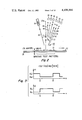
- FIG. 2 similar to FIG. 1(b) of the Applied Optics Article, illustrates a grating test pattern 20 formed, for example, by etching a surface 22 of a substrate 24 of silicon.
- the pattern 20 is formed of a series of parallel lines or strips 21 seen in edge view in FIG. 2 having a width a, a thickness w, and a periodicity of d.
- Monochromatic light illuminates the grating from a laser 26 providing a beam 28 which strikes the grating 20, causing a reflection of signals of various diffraction orders identified as zero order [I(0)] beam 40, positive first order [I(1)] beam 41, positive second order [I(2)] beam 42, positive n order [I(n)] beam, negative first order [I(1)] beam 43 and negative second order [I(2)] beam 44 where n is an integer.
- the positive and negative order beams are so designated merely to relate in space to the zero order beam 40 as the reference location. Other diffractions may exist and may be utilized, but are not shown.
- the intensity of the several diffracted beams are detected by associated silicon detectors 30-35 suitably positioned in the reflected beam pattern of diffracted beams to receive optical signals corresponding to the desired order to be detected.
- the laser beam at incident angle ⁇ i relative to the nornal 22a causes diffraction signals along angle ⁇ 1 , ⁇ 2 , etc.
- the reliability of the laser for use with the diffraction grating is improved by avoiding internal reflections. Accordingly, as known in the art, the angle of incidence for minimum disturbing reflections is the Brewster angle such that:
- ⁇ is the incidence angle
- n s is the refractive index of the material of the grating strips 21 and wherein the polarization of the beam 28 is in the plane of the incidence.
- the laser beam when disposed as shown in FIG. 2, provides diffraction patterns that are in the reflective mode.
- a wafer is formed entirely of such a diffraction pattern to serve as the test sample according to the invention, indicated as test sample 200 shown in FIG. 4.
- FIG. 3 is a plot of a rectangular grating profile useful in understanding the principles of the invention.
- the reflection of the laser beam 28 from the grating 20 results in the diffraction orders illustrated in FIG. 2.
- the intensity of the diffraction orders are determined by the detailed shape of the grating profile 20. If the grating period d is large compared to the wavelength of the laser beam 28, and if the grating profile is not too deep (dimension w), the scalar diffraction theory of Kirchoff and Fraunhofer can be used. This scalar theory is well known. Reference is made to any standard text on the subject, for example, Principles of Optics, by M. Born and E.
- the amplitudes of diffraction orders are proportional to the Fourier amplitudes of the reflectivity profile of the grating (20).
- the theory becomes particularly simple if the grating profile is a rectangular wave, that is, if the absolute magnitude and phase of the reflectivity r(x) are rectangular functions of x.
- x is the coordinate in the plane of the grating running perpendicular to the grating line. As shown in FIG. 2, x is the direction of the movement of the grating 20 under the line beam 28 for this embodiment.
- the rectangular functions of x are described from the following equation:
- r is the reflectivity and ⁇ is the phase angle.
- the absolute value of the reflectivity r is plotted showing the width a and the periodicity d as well as the phase ⁇ in the lower plot of FIG. 3.
- the ratio of the second to the first order intensity signals as detected by detectors 32 and 31, respectively, as shown in FIG. 2 can be represented as follows:
- d is the grating (period) periodicity.
- a is, in fact, the average width of all of the grating lines of that part of the grating 20 which is exposed to the laser beam 28.
- the diffraction grating 20 is made to comprise the whole area of a mask or wafer that is to be used for monitoring the image transfer process described hereinabove (FIG. 1).
- the diameter of the laser beam 28 is made small enough to resolve local line width variations but still large enough to comprise many grating lines 21, e.g., 100 lines 21. It has been discovered that this will provide well-defined diffraction orders and a good average with respect to the line width a.
- the ratio of a/d is, for this embodiment, 1/4 which provides the best sensitivity as indicated by equation (3) described hereinabove. Accordingly, with a laser beam 28 of 1 millimeter in diameter, the apparatus provides a means to measure the average of over 100 grating lines 21 with good resolution.
- the time required for taking a typical scan plot such a shown in FIG. 5, to be described, is 40 minutes for laboratory type equipment. This scanning time can be reduced particularly if fewer lines of scan are required or by using more rapidly responding detectors and data processing as will be illustrated in FIG. 11.
- FIG. 4 illustrates in schematic form the apparatus used to provide the scan plot such as illustrated in FIG. 5 for determining line width, line thickness and line edge profile.
- FIG. 4 The apparatus of FIG. 4 is simplified to provide only the first [I(1)] and second [I(2)] order diffraction signals to determine line width. Higher order positive or negative signals [I(n)] as well as the zero order signal [I(0)] will be provided in such apparatus to determine line depth and profile as will be further described.
- FIG. 11 illustrates a system using n diffraction orders processed with digital signals.
- the mask or wafer 200 is formed with a grating pattern 20 (FIG. 2) extending over the entire surface thereof and is supported on a stage 50 oriented in a vertical position in the y direction of line 21.
- the stage 50 is supported on a carriage 52 by guide rod support members 54.
- the stage 50 is moved in a horizontal x direction by a motor 56 and in a y direction by a motor 58.
- Motors 56 and 58 can be stepping motors by which the respective x and y positions of the wafer 200 can be determined by the number of steps each motor is moved.
- the motors can be d.c. motors provided with potentiometers or encoders to provide x and y positional information signals.
- Laser 26 preferably a red He-Ne laser having a wavelength ⁇ , equal to 0.6328 micrometers, provides a beam 28a, which is polarized in the direction indicated by arrow 60, chopped to 1,000 Hz by a chopper 62, collimated by a beam collimator 64 and thence reflected by a mirror 66 as beam 28b to the mask or wafer 200.
- Stage 50 is also provided with a template or reference pattern 68 carried by extended support 70 attached to stage 50. Attached to the stage 50 are several other templates to control the pen of the recorder 80. Template 68 follows the x and y-motions of the carriage 50 and is shaped to correspond to that of the wafer or mask 200.
- An optical edge sensor 72 generates a signal when the laser beam 28b reaches the edge of the wafer 200 by sensing the corresponding edge of template 68.
- the sensor 72 is suitably displaced in a fixed position from the position of the beam to accurately correspond to the movement of the wafer 200. Signals from the sensor 72 are applied to a circuit of logic 74 for controlling solenoid 91 for switches 89 and 88 and the lift pen via bus 80b.
- the solenoid 91 will maintain the switches 88 and 89 as shown and the pen will be in position for writing.
- the template 76 follows only the x-motion of the stage 50.
- the reference marks 76a and 76b on template 76 are used to draw the base line scales 97 and 98 by recorder 80 as shown in FIG. 5 also.
- the sensor 78 senses the template portions 76a and 76b to provide signals to logic 74 to control solenoid 91 and thus switches 88 and 89.
- logic 74 provides a control signal in response to the detector 78 to the lift pen operation of the recorder 80 via bus 80b.
- the edge sensor 72 is used to lift the recorder pen when the laser beam is not on the wafer 200.
- This lift signal is overwritten by the base line scale sensor 78 to drop the pen for automatically drawing the base line scales 97 and 98 before and after each scan.
- the lift pen command is also provided by the comparator logic 104 responsive to the diffraction order signals, for example, I(1), I(2)/I(1).
- the comparator logic 104 responsive to the diffraction order signals, for example, I(1), I(2)/I(1).
- non-valid data can automatically be eliminated from the scan plots for diffraction orders I(1) smaller than a given level e.g., less than 0.1 V and/or for diffraction order I(2) values larger than I(1).
- the pen is lifted for diffraction signals by which I(1) is less than 0.1 V and I(2) is greater than I(1). Further discussions on this feature are illustrated in FIGS. 6 and 7 to be described.
- the position of the beam 28b on the wafer 200 is traced by the position of the pen, not shown, on the x-y recorder 80.
- the detectors 31 and 32 preferably silicon photodiodes, are positioned to intersect the first and second order beams 41 and 42 from the grating 20 of the wafer 200.
- the output signals of these two detectors are proportional to I(1) and I(2), respectively and are rectified by phase sensitive amplifiers (PSA) 82 and 84, respectively, the respective outputs of the PSA amplifiers 82 and 84 are applied to a divider circuit 86 through the normally closed switches 88 and 89 to provide a signal on path 86a representing I(2)/I(1).
- PSA phase sensitive amplifier
- This ratio signal is added to the y-input of the recorder 80 at summer 107 after attenuation by attenuator 90.
- Attenuator 90 serves to reduce the level of output divider 86 (typically 10 volts) for coupling to the summer 107 and subsequently the y-input to the recorder 80.
- motors 56 and 58 with suitable position control, as by an encoder, etc., cause the wafer to be moved first in an x-direction across the wafer in a direction transverse the grating lines 20 to develop a first scan line preferably at the bottom such as scan line 92 as shown in FIG. 5.
- Motor 56 is returned to the initial x-position and motor 58 causes the wafer 200 to be displaced in a downward, vertical direction so that the next line 94 is scanned.
- a position signal from motor 56 is carried on path 56a and passed through summer 107, applying the signal to the x-input of recorder 80.
- Block 108 represents a bias voltage source potentiometer for providing horizontal lines for the micron scale 96 on the chart for measurement purposes.
- the numbers “0, 1, 2, 3 and 4" and the legend " ⁇ m" are later added by hand.
- the line width scale lines 97 and 98 generated at the left and right borders of the scan line are spaced at 2 mm intervals. This represents the system sampling interval of the entire surface of the wafer 200 of nominal size of 70 mm (2.75 inches) with scan lines that are nominally 2 mm apart.
- rounded grating lines will cause anomalous diffraction signal ratios manifested by poorly defined edges. This condition is identified by sharply deviating and therefore erratic scan lines. Whether or not the contour of the grating line can be defined, the fact that the grating line profile is significantly departing from the desired rectangular edge is significantly important to known in IC processing.
- FIG. 5 for a description of the format of a scan plot 110.
- the scales 97 and 98 are graded with lines that are spaced two millimeters.
- the starting and ending y-location base lines 97a and 98a are the references for the first scan 92. Every fifth scan line with its corresponding base line is indicated by the dashed lines 98b, 98c, 98d, etc.
- the ratio of the diffraction orders I(2)/I(1) is plotted for each of the base lines in a positive direction starting with the zero millimeter base line 97a.
- the line width from a given point on the plot shown in FIG. 5 corresponding marks on the two y scales 97 and 98 are connected by a hand-drawn line as with a straight edge.
- the distance at the desired x-position between the corresponding base line and the scan line, for example, is measured.
- all values of I(2)/I(1) are smaller than 0.5. In other words, all the line widths scanned are larger than 2 micrometers.
- the plot 110 of FIG. 5 illustrates how the line width values of a specimen wafer 200 are extracted from, for convenience, five standard reference positions which are indicated on FIG.
- the measured value of the line width at point 112, for example, is 2.4 ⁇ m being the plot distance from point 112 to point 112a is applied to scale 96 measured downward from the "2" ⁇ m reference line.
- Point 112a is at the intersection of the line drawn between the two 62 mm lines on scales 97 and 98 and the vertical line 110a.
- the average line width of the five values at points 112-120 may be conveniently called or identified as a.
- the wafer plot 110 excluding a 10 millimeter wide rim to exclude abnormality of charting, the highest and lowest line width readings which are a max and a min , respectively and marked for this particular wafer as points 121 and 122.
- Enumerable scan plots can be made of wafers, masks and the like that may vary in appearance from that shown in FIG. 5 very drastically. Experiments with the equipment providing these scan plots will readilly demonstrate such variations to those of ordinary skill in this art in view of the description herein. Several more examples are illustrated for illustrative purposes only and not by way of limitation of the kinds of scan plots that the apparatus of the invention can provide.
- the grating lines 21 are not completely rectangular in cross section as shown in FIG. 2. This results in a contribution to the diffraction curves 134 and 136 for which equation (3), supra, does not apply.
- This type of error is small under normal circumstances. However, this error becomes large due to interference effects if the regular (non-edge) part of the diffraction signals I(1) and I(2) is small. Accordingly, comparator logic 104 is arranged to provide a signal to lift the recorder pen whenever the diffraction signal I(1) is below a given level.
- Points 138 were determined from microscope studies of the actual contour that should have been produced by the laser scan ending along the dashed line 139 at the 20 mm scale line. Thus, the chart plot 136 is in error. The error is believed to be due to the 12,000 angstroms thick aluminum lines. If the lines had been only 6,000 angstroms thick, the plot would have been valid, i.e. points 138 would have followed line 139. Nevertheless, the plot 136 is useful as a first order approximation for determining the line width of the grating.
- the curve plot 140 shown in FIG. 9 in which the ridge 142 shows a 0.2 micrometer error along a portion of the wafer is an illustration of the extremely excellent sensitivity the wafer scanning technique provides.
- FIG. 10 is a curve plot 124' of the wafer that is illustrated by scan 124 in FIG. 6.
- the blank portions 126a, 128a and 130a were caused by the pen being lifted from the recorder while portions 126, 128 and 130, (shown in FIG. 6) respectively, were being scanned. Since the conditions set forth in FIG. 4 for the lift pen control were violated, the pen was lifted.
- the line width of a specimen monitor wafer 200 formed entirely of diffraction gratings 20 may be scanned to determine the line width of the grating at that particular stage of the image transfer process described above and outlined by the flow chart illustrated in FIG. 1.
- the depth of the grating lines can be determined by a measurement of the zero order diffraction signal I(0) and one or more of the higher order diffraction signals I(1), I(2), I(3), I(n) etc. Any one of such ratios can be measured by suitable implementation of the apparatus shown in FIG. 4.
- the invention can provide during the scan plot of a particular monitor wafer the edge profile of the grating lines 21.
- the edge profile is a deviation from the square wave profile illustrated in FIG. 3. Deviation from the square wave profile will be manifested in a loss of the expected ratio between three or more sets of diffraction orders.
- the invention provides a means for determining gross imperfections in the diffraction grating 20 to indicate process errors.
- Gross errors in the diffraction pattern are readily discernible to the naked eye of an observer.
- the sample wafer or mask of the present invention provides a means to determine rapidly such gross errors by providing thereby a visually discernible map of a defective portion of the wafer.
- the apparatus shown in FIG. 4 may be arranged into an image processing system to utilize digital signal format for processing by a computer to generate therefrom information in the form of a printed copy of data indicative of the line parameter information that is determined from a scan of a wafer.
- the system provides a means for having a display of the data on a real or stored time basis on a CRT and, if desired, a chart recorder as described hereinabove and shown in the embodiment in FIG. 4.
- such a modified system is arranged to include the laser 26 generating a beam 28b by reflection from the mirror 66 to a wafer 180 mounted on the x-y moving structure 50.
- the diffracted beams 40 . . . 46, etc. are sensed by, for example, detectors 30, 31, 32, 33, 34 (shown in FIG. 2), as well as higher order diffraction signal detectors 33 and 39.
- the detected signals are passed to a high speed analog to digital converter (A/D) 150 to provide digital signals to a computer 153 via bus 152.
- a memory 154 is coupled via bus 156 to the computer 153.
- Positional signals in analog form from the x-motor 56 and y-motor 58 are applied to the A/D converter 150.
- Control electronics 158 under control of an operator's console 160 is used to monitor the operation of the system via bus 159.
- a printer 164 receives suitable control signals from the computer 153 to provide a hard-copy, print-out of data corresponding to each scan.
- a CRT 166 may be used to provide a means to monitor the contour lines without using a chart recorder, or, as previously described, a chart recorder 168 can be used in the system in the manner described in detail for the use of the chart recorder 80 shown in FIG. 4.
- a wafer 180 is positioned on the apparatus 50 for scanning by the incident laser beam 28b.
- the diffraction signals I(0) . . . I(n) are detected and passed to the high speed A/D converter 150 and thence to the computer 153 for storage and analysis.
- the data is stored in a memory 154 location representing the first stage (1) of a plurality of stages that the wafer 180 is to be processed.
- the wafer After the wafer has been removed from the equipment and processed along with the product wafers, at a selected stage the wafer will then be placed on the equipment holder 50 for a monitor scan. The results of this scan are stored in memory 154 location 2.
- the wafer is processed from stage-to-stage and scanned to provide additional line parameter information for storage in location 3.
- the computer will be controlled to provide computations of the difference of each line at a given stage to the parameters of that same line at a subsequent stage.
- This information can be displayed on the CRT or tabulated in any form desirable and produced on a hard copy by printer 164 for subsequent study. It will be appreciated that either of the chart recorders 168 or 80 can be used only to provide a record of a scan of the particular wafer. However a plot on recorder 168 of the line width differences alone between stages can be made, in which computer 153 performs the linewidth difference calculations.
- the diffraction orders used in the computation depends on what parameter of the line one wants to compare. As described above, the ratio of the first to second order diffraction signals is used to determine line width. The ratio of one or more of those or other diffraction signals can be used to indicate the profile of the lines relative to the rectangular form (FIG. 3). Mathematically the profile relationship can be represented as follows:
- n, m and j are integers and different diffraction orders.
- the 0 order diffraction signal is needed.
- the relationship of the thickness is represented by the relationship:
- the data derived from a scan of the test sample to determine depth deviations, and profile deviations, derived from an analysis of the diffraction signals defined by equations 4 and 5 are preferably processed in numerical form. While visual displays on the chart recorder and/or the CRT will be useful in evaluating each computation, only one set of ratios can be displayed at a time in order to avoid confusion in the display.
- the invention provides a means for following the LSI fabrication process on a stage-by-stage basis, i.e. the development of an integrated circuit for LSI from the conceptual computer form to the final LSI device.
- Each stage of the process uses a grating test mask or wafer which can be processed as a monitor with the desired product wafers or masks.
- the monitor wafer having the preformed grating can be evaluated stage-by-stage for degradation of the line widths. These degradations can then be used as a fair measurement of the degradation of the actual LSI wafer or mask of predetermined circuit form.
- the stage between the mask (12-FIG. 1) to the photoresist stage (14) manifests the most major degradations.
- the invention is quite useful for monitoring the fabrication of masks, silicon film and oxide film lines.
- the invention is not suitable for lines made of aluminum and photoresist on aluminum film at least to the extent as explained in detail hereinabove.
Abstract
Description
tan ξ=n.sub.s (1)
r(x)=r(x) exp [iφ(x)] (2)
I(2)/I(1)=COS.sup.2 (πa/d) (3)
Profile=f[I(n)/I(m), I(j)/I(m) . . . ] (4)
Thickness=f[I(0)/I(n)] (5)
Claims (21)
Priority Applications (1)
| Application Number | Priority Date | Filing Date | Title |
|---|---|---|---|
| US06/278,448 US4408884A (en) | 1981-06-29 | 1981-06-29 | Optical measurements of fine line parameters in integrated circuit processes |
Applications Claiming Priority (1)
| Application Number | Priority Date | Filing Date | Title |
|---|---|---|---|
| US06/278,448 US4408884A (en) | 1981-06-29 | 1981-06-29 | Optical measurements of fine line parameters in integrated circuit processes |
Publications (1)
| Publication Number | Publication Date |
|---|---|
| US4408884A true US4408884A (en) | 1983-10-11 |
Family
ID=23065014
Family Applications (1)
| Application Number | Title | Priority Date | Filing Date |
|---|---|---|---|
| US06/278,448 Expired - Lifetime US4408884A (en) | 1981-06-29 | 1981-06-29 | Optical measurements of fine line parameters in integrated circuit processes |
Country Status (1)
| Country | Link |
|---|---|
| US (1) | US4408884A (en) |
Cited By (118)
| Publication number | Priority date | Publication date | Assignee | Title |
|---|---|---|---|---|
| US4623403A (en) * | 1984-06-15 | 1986-11-18 | Texas Instruments Incorporated | Indexing of laser beam for programming VLSI devices |
| US4645349A (en) * | 1984-09-21 | 1987-02-24 | O R C Manufacturing Co., Ltd. | Method of measuring film thickness |
| US4683420A (en) * | 1985-07-10 | 1987-07-28 | Westinghouse Electric Corp. | Acousto-optic system for testing high speed circuits |
| US4703434A (en) * | 1984-04-24 | 1987-10-27 | The Perkin-Elmer Corporation | Apparatus for measuring overlay error |
| US4714826A (en) * | 1986-08-18 | 1987-12-22 | Westinghouse Electric Corp. | Apparatus and method for testing outputs of logic circuits by modulating optical sequals |
| US4777146A (en) * | 1987-02-24 | 1988-10-11 | American Telephone And Telegraph Company, At&T Bell Laboratories | Fabrication process involving semi-insulating material |
| US4806457A (en) * | 1986-04-10 | 1989-02-21 | Nec Corporation | Method of manufacturing integrated circuit semiconductor device |
| US4874941A (en) * | 1988-05-11 | 1989-10-17 | Simmonds Precision Products, Inc. | Optical displacement sensor with a multi-period grating |
| US4964726A (en) * | 1988-09-27 | 1990-10-23 | General Electric Company | Apparatus and method for optical dimension measurement using interference of scattered electromagnetic energy |
| US5002631A (en) * | 1990-03-09 | 1991-03-26 | At&T Bell Laboratories | Plasma etching apparatus and method |
| US5076692A (en) * | 1990-05-31 | 1991-12-31 | Tencor Instruments | Particle detection on a patterned or bare wafer surface |
| EP0480620A2 (en) * | 1990-10-09 | 1992-04-15 | AT&T Corp. | Method for inspecting etched workpieces |
| US5162240A (en) * | 1989-06-16 | 1992-11-10 | Hitachi, Ltd. | Method and apparatus of fabricating electric circuit pattern on thick and thin film hybrid multilayer wiring substrate |
| US5229303A (en) * | 1989-08-29 | 1993-07-20 | At&T Bell Laboratories | Device processing involving an optical interferometric thermometry using the change in refractive index to measure semiconductor wafer temperature |
| EP0585839A2 (en) * | 1992-08-31 | 1994-03-09 | Texas Instruments Incorporated | Process control for submicron linewidth measurement |
| EP0595020A2 (en) * | 1992-09-21 | 1994-05-04 | Texas Instruments Incorporated | Process control for submicron linewidth measurement |
| US5357335A (en) * | 1993-03-31 | 1994-10-18 | Minnesota Mining And Manufacturing Company | Optical detection device for screening magnetic tape |
| US5384639A (en) * | 1992-05-13 | 1995-01-24 | International Business Machines Corporation | Depth measurement of high aspect ratio structures |
| US5629801A (en) * | 1995-06-07 | 1997-05-13 | Silicon Light Machines | Diffraction grating light doubling collection system |
| US5661592A (en) * | 1995-06-07 | 1997-08-26 | Silicon Light Machines | Method of making and an apparatus for a flat diffraction grating light valve |
| DE19632763A1 (en) * | 1996-08-14 | 1998-02-26 | Holger Moritz | Measurement head for monitoring development of photoresist |
| US5757494A (en) * | 1994-10-21 | 1998-05-26 | J.A. Woollam Co. Inc. | System and method for improving data acquisition capability in spectroscopic ellipsometers |
| US5798743A (en) * | 1995-06-07 | 1998-08-25 | Silicon Light Machines | Clear-behind matrix addressing for display systems |
| US5808797A (en) * | 1992-04-28 | 1998-09-15 | Silicon Light Machines | Method and apparatus for modulating a light beam |
| US5841579A (en) * | 1995-06-07 | 1998-11-24 | Silicon Light Machines | Flat diffraction grating light valve |
| US5862058A (en) * | 1996-05-16 | 1999-01-19 | International Business Machines Corporation | Optical proximity correction method and system |
| US5940194A (en) * | 1996-10-22 | 1999-08-17 | University Of Delaware | Real time-determination of interconnect metrology using binary computer-generated holograms |
| DE19806288A1 (en) * | 1998-02-16 | 1999-08-26 | Fraunhofer Ges Forschung | Laser scanner measuring system |
| US5963329A (en) * | 1997-10-31 | 1999-10-05 | International Business Machines Corporation | Method and apparatus for measuring the profile of small repeating lines |
| US5969273A (en) * | 1998-02-12 | 1999-10-19 | International Business Machines Corporation | Method and apparatus for critical dimension and tool resolution determination using edge width |
| US5982489A (en) * | 1996-01-29 | 1999-11-09 | Nikon Corporation | Method and apparatus for measuring depth of a depression in a pattern by light interference from crossed light beams |
| US5982553A (en) * | 1997-03-20 | 1999-11-09 | Silicon Light Machines | Display device incorporating one-dimensional grating light-valve array |
| US6064404A (en) * | 1996-11-05 | 2000-05-16 | Silicon Light Machines | Bandwidth and frame buffer size reduction in a digital pulse-width-modulated display system |
| US6088102A (en) * | 1997-10-31 | 2000-07-11 | Silicon Light Machines | Display apparatus including grating light-valve array and interferometric optical system |
| US6101036A (en) * | 1998-06-23 | 2000-08-08 | Silicon Light Machines | Embossed diffraction grating alone and in combination with changeable image display |
| US6130770A (en) * | 1998-06-23 | 2000-10-10 | Silicon Light Machines | Electron gun activated grating light valve |
| US6215579B1 (en) | 1998-06-24 | 2001-04-10 | Silicon Light Machines | Method and apparatus for modulating an incident light beam for forming a two-dimensional image |
| US6271808B1 (en) | 1998-06-05 | 2001-08-07 | Silicon Light Machines | Stereo head mounted display using a single display device |
| US6358860B1 (en) * | 1999-10-07 | 2002-03-19 | Vlsi Standards, Inc. | Line width calibration standard manufacturing and certifying method |
| US6423977B1 (en) * | 1997-02-26 | 2002-07-23 | Kabushiki Kaisha Toshiba | Pattern size evaluation apparatus |
| US20020098610A1 (en) * | 2001-01-19 | 2002-07-25 | Alexander Payne | Reduced surface charging in silicon-based devices |
| US6429943B1 (en) * | 2000-03-29 | 2002-08-06 | Therma-Wave, Inc. | Critical dimension analysis with simultaneous multiple angle of incidence measurements |
| US6483580B1 (en) | 1998-03-06 | 2002-11-19 | Kla-Tencor Technologies Corporation | Spectroscopic scatterometer system |
| US20020171830A1 (en) * | 1998-04-08 | 2002-11-21 | Norton Adam E. | Spectroscopic measurement system using an off-axis spherical mirror and refractive elements |
| US6489624B1 (en) * | 1997-07-18 | 2002-12-03 | Nikon Corporation | Apparatus and methods for detecting thickness of a patterned layer |
| US6493073B2 (en) * | 2000-12-11 | 2002-12-10 | Sheldon L. Epstein | System and method for measuring properties of an optical component |
| US20020196492A1 (en) * | 2001-06-25 | 2002-12-26 | Silicon Light Machines | Method and apparatus for dynamic equalization in wavelength division multiplexing |
| US20030025984A1 (en) * | 2001-08-01 | 2003-02-06 | Chris Gudeman | Optical mem device with encapsulated dampening gas |
| US20030035189A1 (en) * | 2001-08-15 | 2003-02-20 | Amm David T. | Stress tuned blazed grating light valve |
| US20030048458A1 (en) * | 2001-06-26 | 2003-03-13 | Walter Mieher | Method for determining lithographic focus and exposure |
| US6538731B2 (en) * | 2001-01-26 | 2003-03-25 | Timbre Technologies, Inc. | System and method for characterizing macro-grating test patterns in advanced lithography and etch processes |
| US20030103194A1 (en) * | 2001-11-30 | 2003-06-05 | Gross Kenneth P. | Display apparatus including RGB color combiner and 1D light valve relay including schlieren filter |
| EP1332330A1 (en) * | 2000-09-06 | 2003-08-06 | Accent Optical Technologies, Inc. | Determination of center of focus by diffraction signature analysis |
| US6611330B2 (en) | 1999-02-09 | 2003-08-26 | Kla-Tencor Corporation | System for measuring polarimetric spectrum and other properties of a sample |
| US20030168594A1 (en) * | 2002-01-22 | 2003-09-11 | Muckenhirn Sylvain G. | Integrated measuring instrument |
| US6628409B2 (en) * | 2000-11-23 | 2003-09-30 | Infineon Technologies Ag | Method for determining the distance between periodic structures on an integrated circuit or a photomask |
| US20030200047A1 (en) * | 2002-04-18 | 2003-10-23 | Seh America, Inc. | Methods and computer program products for characterizing a crystalline structure |
| US6658144B1 (en) * | 1997-05-23 | 2003-12-02 | Micron Technology, Inc. | Diffraction tomography for monitoring latent image formation |
| EP1370828A1 (en) * | 2001-03-02 | 2003-12-17 | Accent Optical Technologies, Inc. | Line profile asymmetry measurement using scatterometry |
| US20040001257A1 (en) * | 2001-03-08 | 2004-01-01 | Akira Tomita | High contrast grating light valve |
| US20040008399A1 (en) * | 2001-06-25 | 2004-01-15 | Trisnadi Jahja I. | Method, apparatus, and diffuser for reducing laser speckle |
| US6707591B2 (en) | 2001-04-10 | 2004-03-16 | Silicon Light Machines | Angled illumination for a single order light modulator based projection system |
| US6713753B1 (en) | 2001-07-03 | 2004-03-30 | Nanometrics Incorporated | Combination of normal and oblique incidence polarimetry for the characterization of gratings |
| US6712480B1 (en) | 2002-09-27 | 2004-03-30 | Silicon Light Machines | Controlled curvature of stressed micro-structures |
| US6714337B1 (en) | 2002-06-28 | 2004-03-30 | Silicon Light Machines | Method and device for modulating a light beam and having an improved gamma response |
| US6728023B1 (en) | 2002-05-28 | 2004-04-27 | Silicon Light Machines | Optical device arrays with optimized image resolution |
| EP1436670A2 (en) * | 2001-10-10 | 2004-07-14 | Accent Optical Technologies, Inc. | Determination of center of focus by cross-section analysis |
| US6764875B2 (en) | 1998-07-29 | 2004-07-20 | Silicon Light Machines | Method of and apparatus for sealing an hermetic lid to a semiconductor die |
| US6767751B2 (en) | 2002-05-28 | 2004-07-27 | Silicon Light Machines, Inc. | Integrated driver process flow |
| US6771356B1 (en) * | 2002-01-16 | 2004-08-03 | Advanced Micro Devices, Inc. | Scatterometry of grating structures to monitor wafer stress |
| US6773939B1 (en) * | 2001-07-02 | 2004-08-10 | Advanced Micro Devices, Inc. | Method and apparatus for determining critical dimension variation in a line structure |
| US6800238B1 (en) | 2002-01-15 | 2004-10-05 | Silicon Light Machines, Inc. | Method for domain patterning in low coercive field ferroelectrics |
| US6801354B1 (en) | 2002-08-20 | 2004-10-05 | Silicon Light Machines, Inc. | 2-D diffraction grating for substantially eliminating polarization dependent losses |
| US6806997B1 (en) | 2003-02-28 | 2004-10-19 | Silicon Light Machines, Inc. | Patterned diffractive light modulator ribbon for PDL reduction |
| DE10315086A1 (en) * | 2003-04-02 | 2004-10-21 | Infineon Technologies Ag | Semiconductor wafer alignment method, by correcting optically measured position information for adjustment mark using line profile of adjustment mark |
| US6813059B2 (en) | 2002-06-28 | 2004-11-02 | Silicon Light Machines, Inc. | Reduced formation of asperities in contact micro-structures |
| US20040218192A1 (en) * | 2003-05-02 | 2004-11-04 | Joerg Bischoff | Edge roughness measurement in optical metrology |
| US6822797B1 (en) | 2002-05-31 | 2004-11-23 | Silicon Light Machines, Inc. | Light modulator structure for producing high-contrast operation using zero-order light |
| US6829092B2 (en) | 2001-08-15 | 2004-12-07 | Silicon Light Machines, Inc. | Blazed grating light valve |
| US6829258B1 (en) | 2002-06-26 | 2004-12-07 | Silicon Light Machines, Inc. | Rapidly tunable external cavity laser |
| US6865346B1 (en) * | 2001-06-05 | 2005-03-08 | Silicon Light Machines Corporation | Fiber optic transceiver |
| US6898537B1 (en) | 2001-04-27 | 2005-05-24 | Nanometrics Incorporated | Measurement of diffracting structures using one-half of the non-zero diffracted orders |
| US20050128487A1 (en) * | 2003-01-27 | 2005-06-16 | Zetetic Institute | Leaky guided wave modes used in interferometric confocal microscopy to measure properties of trenches |
| US6949462B1 (en) | 2002-04-04 | 2005-09-27 | Nanometrics Incorporated | Measuring an alignment target with multiple polarization states |
| US6956878B1 (en) | 2000-02-07 | 2005-10-18 | Silicon Light Machines Corporation | Method and apparatus for reducing laser speckle using polarization averaging |
| US6982793B1 (en) | 2002-04-04 | 2006-01-03 | Nanometrics Incorporated | Method and apparatus for using an alignment target with designed in offset |
| US6987600B1 (en) | 2002-12-17 | 2006-01-17 | Silicon Light Machines Corporation | Arbitrary phase profile for better equalization in dynamic gain equalizer |
| US6992764B1 (en) | 2002-09-30 | 2006-01-31 | Nanometrics Incorporated | Measuring an alignment target with a single polarization state |
| US20060033924A1 (en) * | 2004-08-16 | 2006-02-16 | Zetetic Institute | Apparatus and method for joint and time delayed measurements of components of conjugated quadratures of fields of reflected/scattered and transmitted/scattered beams by an object in interferometry |
| US20060050283A1 (en) * | 2004-08-19 | 2006-03-09 | Zetetic Institute | Sub-nanometer overlay, critical dimension, and lithography tool projection optic metrology systems based on measurement of exposure induced changes in photoresist on wafers |
| US20060066873A1 (en) * | 2004-09-20 | 2006-03-30 | Zetetic Institute | Catoptric imaging systems comprising pellicle and/or aperture-array beam-splitters and non-adaptive and/or adaptive catoptric surfaces |
| US20060072204A1 (en) * | 2003-09-26 | 2006-04-06 | Zetetic Institute | Catoptric and catadioptric imaging systems with pellicle and aperture-array beam-splitters and non-adaptive and adaptive catoptric surfaces |
| US20060081790A1 (en) * | 2002-09-20 | 2006-04-20 | Asml Netherlands B.V. | Alignment systems and methods for lithographic systems |
| US7061615B1 (en) | 2001-09-20 | 2006-06-13 | Nanometrics Incorporated | Spectroscopically measured overlay target |
| WO2006080902A2 (en) * | 2004-09-08 | 2006-08-03 | Accent Optical Technologies, Inc. | Method and apparatus for determining line characteristics, e.g., line roughness, of microfeature components |
| JP2006518942A (en) * | 2003-02-22 | 2006-08-17 | ケーエルエー−テンカー テクノロジィース コーポレイション | Apparatus and method for detecting overlay error using scatterometry |
| US7115858B1 (en) | 2000-09-25 | 2006-10-03 | Nanometrics Incorporated | Apparatus and method for the measurement of diffracting structures |
| US20070075037A1 (en) * | 2005-10-05 | 2007-04-05 | Taiwan Semiconductor Manufacturing Co., Ltd. | Dimension monitoring method and system |
| US20070201043A1 (en) * | 2001-03-02 | 2007-08-30 | Accent Optical Technologies, Inc. | Line Profile Asymmetry Measurement |
| US7280230B2 (en) | 2001-12-19 | 2007-10-09 | Kla-Tencor Technologies Corporation | Parametric profiling using optical spectroscopic systems |
| US20080013108A1 (en) * | 2006-07-11 | 2008-01-17 | Tokyo Electron Limited | Parallel profile determination in optical metrology |
| EP1903397A2 (en) * | 2006-09-25 | 2008-03-26 | ASML Netherlands B.V. | Method and apparatus for angular-resolved spectroscopic lithography characterization |
| US20080307910A1 (en) * | 2007-06-15 | 2008-12-18 | Rolls-Royce Plc | Test piece and apparatus for testing |
| US7515253B2 (en) | 2005-01-12 | 2009-04-07 | Kla-Tencor Technologies Corporation | System for measuring a sample with a layer containing a periodic diffracting structure |
| WO2009106253A1 (en) * | 2008-02-27 | 2009-09-03 | Asml Netherlands B.V. | Inspection method and apparatus, lithographic apparatus, lithographic processing cell and device manufacturing method |
| US7650199B1 (en) * | 2005-08-03 | 2010-01-19 | Daniel Kadosh | End of line performance prediction |
| US20100078564A1 (en) * | 2006-01-31 | 2010-04-01 | Polychromix Corporation | Apparatus and method providing a hand-held spectrometer |
| US7891818B2 (en) | 2006-12-12 | 2011-02-22 | Evans & Sutherland Computer Corporation | System and method for aligning RGB light in a single modulator projector |
| US20110245955A1 (en) * | 2010-04-01 | 2011-10-06 | Tokyo Electron Limited | Automated process control using an adjusted metrology output signal |
| KR101071654B1 (en) | 2003-09-12 | 2011-10-11 | 나노메트릭스 인코포레이티드 | Line Profile Asymmetry Measurement |
| US8077378B1 (en) | 2008-11-12 | 2011-12-13 | Evans & Sutherland Computer Corporation | Calibration system and method for light modulation device |
| WO2012084142A1 (en) * | 2010-12-23 | 2012-06-28 | Carl Zeiss Sms Gmbh | Method for characterizing a structure on a mask and device for carrying out said method |
| US8358317B2 (en) | 2008-05-23 | 2013-01-22 | Evans & Sutherland Computer Corporation | System and method for displaying a planar image on a curved surface |
| US20140022563A1 (en) * | 2001-04-10 | 2014-01-23 | Kla-Tencor Corporation | Periodic Patterns and Technique to Control Misalignment Between Two Layers |
| US20140038315A1 (en) * | 2012-08-02 | 2014-02-06 | Laytec Ag | Apparatus and method for measuring the dimensions of 1-dimensional and 0-dimensional nanostructures in real-time during epitaxial growth |
| US8654353B2 (en) | 2010-12-30 | 2014-02-18 | Industrial Technology Research Institute | Measuring method for topography of moving specimen and a measuring apparatus thereof |
| US8702248B1 (en) | 2008-06-11 | 2014-04-22 | Evans & Sutherland Computer Corporation | Projection method for reducing interpixel gaps on a viewing surface |
| US9641826B1 (en) | 2011-10-06 | 2017-05-02 | Evans & Sutherland Computer Corporation | System and method for displaying distant 3-D stereo on a dome surface |
Citations (3)
| Publication number | Priority date | Publication date | Assignee | Title |
|---|---|---|---|---|
| US4180830A (en) * | 1977-06-28 | 1979-12-25 | Rca Corporation | Depth estimation system using diffractive effects of the grooves and signal elements in the grooves |
| US4200396A (en) * | 1977-12-19 | 1980-04-29 | Rca Corporation | Optically testing the lateral dimensions of a pattern |
| US4236823A (en) * | 1978-09-18 | 1980-12-02 | Rca Corporation | Diffractometer for measuring signal depth and width |
-
1981
- 1981-06-29 US US06/278,448 patent/US4408884A/en not_active Expired - Lifetime
Patent Citations (3)
| Publication number | Priority date | Publication date | Assignee | Title |
|---|---|---|---|---|
| US4180830A (en) * | 1977-06-28 | 1979-12-25 | Rca Corporation | Depth estimation system using diffractive effects of the grooves and signal elements in the grooves |
| US4200396A (en) * | 1977-12-19 | 1980-04-29 | Rca Corporation | Optically testing the lateral dimensions of a pattern |
| US4236823A (en) * | 1978-09-18 | 1980-12-02 | Rca Corporation | Diffractometer for measuring signal depth and width |
Non-Patent Citations (5)
| Title |
|---|
| H. P. Kleinknecht and H. Meier, "Linewidth Measurement on IC Masks and Wafers by Grating Test Patterns," Applied Optics, vol. 19, pp. 525-533, (1980). * |
| H. P. Kleinknecht, et al., "Use of Large Area Grating Patterns for Scanning of Linewidth Across IC Masks and Wafers," Abst. S35, p. 203, Europhys. Conf. ESSDERC, Sep. 15-18, 1980, York, England. * |
| Technical Note 1143, mailed Mar. 16, 1976, entitled "Method For Measuring The Average Aperture Size of a Plurality of Apertures in a Kinescope Shadow Mask," by A. H. Firester. * |
| W. E. Ham et al., "A Method for Determining the Sources of LSI Linewidth Errors in IC Processes," Abst. S36, p. 205, Europhys. Conf. ESSDERC, Sep. 15-18, 1980, York, England. * |
| W. R. Roach, et al., "Diffraction Spectometry for VideoDisc Quality Control," RCA Review, vol. 39, Sep. 1978, pp. 472-511. * |
Cited By (205)
| Publication number | Priority date | Publication date | Assignee | Title |
|---|---|---|---|---|
| US4703434A (en) * | 1984-04-24 | 1987-10-27 | The Perkin-Elmer Corporation | Apparatus for measuring overlay error |
| US4623403A (en) * | 1984-06-15 | 1986-11-18 | Texas Instruments Incorporated | Indexing of laser beam for programming VLSI devices |
| US4645349A (en) * | 1984-09-21 | 1987-02-24 | O R C Manufacturing Co., Ltd. | Method of measuring film thickness |
| US4683420A (en) * | 1985-07-10 | 1987-07-28 | Westinghouse Electric Corp. | Acousto-optic system for testing high speed circuits |
| US4806457A (en) * | 1986-04-10 | 1989-02-21 | Nec Corporation | Method of manufacturing integrated circuit semiconductor device |
| US4714826A (en) * | 1986-08-18 | 1987-12-22 | Westinghouse Electric Corp. | Apparatus and method for testing outputs of logic circuits by modulating optical sequals |
| US4777146A (en) * | 1987-02-24 | 1988-10-11 | American Telephone And Telegraph Company, At&T Bell Laboratories | Fabrication process involving semi-insulating material |
| US4874941A (en) * | 1988-05-11 | 1989-10-17 | Simmonds Precision Products, Inc. | Optical displacement sensor with a multi-period grating |
| US4964726A (en) * | 1988-09-27 | 1990-10-23 | General Electric Company | Apparatus and method for optical dimension measurement using interference of scattered electromagnetic energy |
| US5162240A (en) * | 1989-06-16 | 1992-11-10 | Hitachi, Ltd. | Method and apparatus of fabricating electric circuit pattern on thick and thin film hybrid multilayer wiring substrate |
| US5229303A (en) * | 1989-08-29 | 1993-07-20 | At&T Bell Laboratories | Device processing involving an optical interferometric thermometry using the change in refractive index to measure semiconductor wafer temperature |
| US5002631A (en) * | 1990-03-09 | 1991-03-26 | At&T Bell Laboratories | Plasma etching apparatus and method |
| US5076692A (en) * | 1990-05-31 | 1991-12-31 | Tencor Instruments | Particle detection on a patterned or bare wafer surface |
| US5114233A (en) * | 1990-10-09 | 1992-05-19 | At&T Bell Laboratories | Method for inspecting etched workpieces |
| EP0480620A3 (en) * | 1990-10-09 | 1992-09-30 | American Telephone And Telegraph Company | Method for inspecting etched workpieces |
| EP0480620A2 (en) * | 1990-10-09 | 1992-04-15 | AT&T Corp. | Method for inspecting etched workpieces |
| US5808797A (en) * | 1992-04-28 | 1998-09-15 | Silicon Light Machines | Method and apparatus for modulating a light beam |
| US5384639A (en) * | 1992-05-13 | 1995-01-24 | International Business Machines Corporation | Depth measurement of high aspect ratio structures |
| EP0585839A2 (en) * | 1992-08-31 | 1994-03-09 | Texas Instruments Incorporated | Process control for submicron linewidth measurement |
| EP0585839A3 (en) * | 1992-08-31 | 1994-06-08 | Texas Instruments Inc | Process control for submicron linewidth measurement |
| US5361137A (en) * | 1992-08-31 | 1994-11-01 | Texas Instruments Incorporated | Process control for submicron linewidth measurement |
| EP0595020A2 (en) * | 1992-09-21 | 1994-05-04 | Texas Instruments Incorporated | Process control for submicron linewidth measurement |
| EP0595020A3 (en) * | 1992-09-21 | 1995-08-09 | Texas Instruments Inc | Process control for submicron linewidth measurement. |
| US5357335A (en) * | 1993-03-31 | 1994-10-18 | Minnesota Mining And Manufacturing Company | Optical detection device for screening magnetic tape |
| US5757494A (en) * | 1994-10-21 | 1998-05-26 | J.A. Woollam Co. Inc. | System and method for improving data acquisition capability in spectroscopic ellipsometers |
| US5798743A (en) * | 1995-06-07 | 1998-08-25 | Silicon Light Machines | Clear-behind matrix addressing for display systems |
| US5629801A (en) * | 1995-06-07 | 1997-05-13 | Silicon Light Machines | Diffraction grating light doubling collection system |
| US5661592A (en) * | 1995-06-07 | 1997-08-26 | Silicon Light Machines | Method of making and an apparatus for a flat diffraction grating light valve |
| US5841579A (en) * | 1995-06-07 | 1998-11-24 | Silicon Light Machines | Flat diffraction grating light valve |
| US5982489A (en) * | 1996-01-29 | 1999-11-09 | Nikon Corporation | Method and apparatus for measuring depth of a depression in a pattern by light interference from crossed light beams |
| US5862058A (en) * | 1996-05-16 | 1999-01-19 | International Business Machines Corporation | Optical proximity correction method and system |
| DE19632763C2 (en) * | 1996-08-14 | 1998-09-10 | Holger Moritz | Measuring head for the observation of photoresist development |
| DE19632763A1 (en) * | 1996-08-14 | 1998-02-26 | Holger Moritz | Measurement head for monitoring development of photoresist |
| US5940194A (en) * | 1996-10-22 | 1999-08-17 | University Of Delaware | Real time-determination of interconnect metrology using binary computer-generated holograms |
| US6064404A (en) * | 1996-11-05 | 2000-05-16 | Silicon Light Machines | Bandwidth and frame buffer size reduction in a digital pulse-width-modulated display system |
| US6423977B1 (en) * | 1997-02-26 | 2002-07-23 | Kabushiki Kaisha Toshiba | Pattern size evaluation apparatus |
| US5982553A (en) * | 1997-03-20 | 1999-11-09 | Silicon Light Machines | Display device incorporating one-dimensional grating light-valve array |
| US6658144B1 (en) * | 1997-05-23 | 2003-12-02 | Micron Technology, Inc. | Diffraction tomography for monitoring latent image formation |
| US6489624B1 (en) * | 1997-07-18 | 2002-12-03 | Nikon Corporation | Apparatus and methods for detecting thickness of a patterned layer |
| US5963329A (en) * | 1997-10-31 | 1999-10-05 | International Business Machines Corporation | Method and apparatus for measuring the profile of small repeating lines |
| US6088102A (en) * | 1997-10-31 | 2000-07-11 | Silicon Light Machines | Display apparatus including grating light-valve array and interferometric optical system |
| US5969273A (en) * | 1998-02-12 | 1999-10-19 | International Business Machines Corporation | Method and apparatus for critical dimension and tool resolution determination using edge width |
| US6858836B1 (en) | 1998-02-16 | 2005-02-22 | Fraunhofer Gesellschaft Zur Foerderung Der Angewandten Forschung E.V. | Laser scanner measurement system |
| DE19806288A1 (en) * | 1998-02-16 | 1999-08-26 | Fraunhofer Ges Forschung | Laser scanner measuring system |
| US7859659B2 (en) | 1998-03-06 | 2010-12-28 | Kla-Tencor Corporation | Spectroscopic scatterometer system |
| US7173699B2 (en) | 1998-03-06 | 2007-02-06 | Kla-Tencor Technologies Corporation | Spectroscopic scatterometer system |
| US7898661B2 (en) | 1998-03-06 | 2011-03-01 | Kla-Tencor Corporation | Spectroscopic scatterometer system |
| US6590656B2 (en) | 1998-03-06 | 2003-07-08 | Kla-Tencor Corporation | Spectroscopic scatterometer system |
| US6483580B1 (en) | 1998-03-06 | 2002-11-19 | Kla-Tencor Technologies Corporation | Spectroscopic scatterometer system |
| US6583877B2 (en) | 1998-04-08 | 2003-06-24 | Adam E. Norton | Spectroscopic measurement system using an off-axis spherical mirror and refractive elements |
| US20020171830A1 (en) * | 1998-04-08 | 2002-11-21 | Norton Adam E. | Spectroscopic measurement system using an off-axis spherical mirror and refractive elements |
| US6271808B1 (en) | 1998-06-05 | 2001-08-07 | Silicon Light Machines | Stereo head mounted display using a single display device |
| US6130770A (en) * | 1998-06-23 | 2000-10-10 | Silicon Light Machines | Electron gun activated grating light valve |
| US6101036A (en) * | 1998-06-23 | 2000-08-08 | Silicon Light Machines | Embossed diffraction grating alone and in combination with changeable image display |
| US6215579B1 (en) | 1998-06-24 | 2001-04-10 | Silicon Light Machines | Method and apparatus for modulating an incident light beam for forming a two-dimensional image |
| US6764875B2 (en) | 1998-07-29 | 2004-07-20 | Silicon Light Machines | Method of and apparatus for sealing an hermetic lid to a semiconductor die |
| US6611330B2 (en) | 1999-02-09 | 2003-08-26 | Kla-Tencor Corporation | System for measuring polarimetric spectrum and other properties of a sample |
| US6358860B1 (en) * | 1999-10-07 | 2002-03-19 | Vlsi Standards, Inc. | Line width calibration standard manufacturing and certifying method |
| US6956878B1 (en) | 2000-02-07 | 2005-10-18 | Silicon Light Machines Corporation | Method and apparatus for reducing laser speckle using polarization averaging |
| US6654131B2 (en) * | 2000-03-29 | 2003-11-25 | Therma-Wave, Inc. | Critical dimension analysis with simultaneous multiple angle of incidence measurements |
| US20060012803A1 (en) * | 2000-03-29 | 2006-01-19 | Jon Opsal | Critical dimension analysis with simultaneous multiple angle of incidence measurements |
| US6972852B2 (en) | 2000-03-29 | 2005-12-06 | Therma-Wave, Inc. | Critical dimension analysis with simultaneous multiple angle of incidence measurements |
| US20040046968A1 (en) * | 2000-03-29 | 2004-03-11 | Jon Opsal | Critical dimension analysis with simultaneous multiple angle of incidence measurements |
| US6829057B2 (en) * | 2000-03-29 | 2004-12-07 | Therma-Wave, Inc. | Critical dimension analysis with simultaneous multiple angle of incidence measurements |
| US6429943B1 (en) * | 2000-03-29 | 2002-08-06 | Therma-Wave, Inc. | Critical dimension analysis with simultaneous multiple angle of incidence measurements |
| US7248375B2 (en) | 2000-03-29 | 2007-07-24 | Therma-Wave, Inc. | Critical dimension analysis with simultaneous multiple angle of incidence measurements |
| US20020135783A1 (en) * | 2000-03-29 | 2002-09-26 | Jon Opsal | Critical dimension analysis with simultaneous multiple angle of incidence measurements |
| US20050057760A1 (en) * | 2000-03-29 | 2005-03-17 | Jon Opsal | Critical dimension analysis with simultaneous multiple angle of incidence measurements |
| EP1332330A4 (en) * | 2000-09-06 | 2006-05-10 | Accent Optical Tech Inc | Determination of center of focus by diffraction signature analysis |
| EP1332330A1 (en) * | 2000-09-06 | 2003-08-06 | Accent Optical Technologies, Inc. | Determination of center of focus by diffraction signature analysis |
| US7115858B1 (en) | 2000-09-25 | 2006-10-03 | Nanometrics Incorporated | Apparatus and method for the measurement of diffracting structures |
| US7372565B1 (en) | 2000-09-25 | 2008-05-13 | Nanometrics Incorporated | Spectrometer measurement of diffracting structures |
| US6628409B2 (en) * | 2000-11-23 | 2003-09-30 | Infineon Technologies Ag | Method for determining the distance between periodic structures on an integrated circuit or a photomask |
| US6493073B2 (en) * | 2000-12-11 | 2002-12-10 | Sheldon L. Epstein | System and method for measuring properties of an optical component |
| US20020098610A1 (en) * | 2001-01-19 | 2002-07-25 | Alexander Payne | Reduced surface charging in silicon-based devices |
| US6538731B2 (en) * | 2001-01-26 | 2003-03-25 | Timbre Technologies, Inc. | System and method for characterizing macro-grating test patterns in advanced lithography and etch processes |
| US6750961B2 (en) | 2001-01-26 | 2004-06-15 | Timbre Technologies, Inc. | System and method for characterizing macro-grating test patterns in advanced lithography and etch processes |
| US20030133104A1 (en) * | 2001-01-26 | 2003-07-17 | Xinhui Niu | System and method for characterizing macro-grating test patterns in advanced lithography and etch processes |
| US20070201043A1 (en) * | 2001-03-02 | 2007-08-30 | Accent Optical Technologies, Inc. | Line Profile Asymmetry Measurement |
| EP1370828A4 (en) * | 2001-03-02 | 2007-03-21 | Accent Optical Tech Inc | Line profile asymmetry measurement using scatterometry |
| US7515279B2 (en) | 2001-03-02 | 2009-04-07 | Nanometrics Incorporated | Line profile asymmetry measurement |
| US7639371B2 (en) | 2001-03-02 | 2009-12-29 | Nanometrics Incorporated | Line profile asymmetry measurement |
| EP1370828A1 (en) * | 2001-03-02 | 2003-12-17 | Accent Optical Technologies, Inc. | Line profile asymmetry measurement using scatterometry |
| US20040001257A1 (en) * | 2001-03-08 | 2004-01-01 | Akira Tomita | High contrast grating light valve |
| US20140022563A1 (en) * | 2001-04-10 | 2014-01-23 | Kla-Tencor Corporation | Periodic Patterns and Technique to Control Misalignment Between Two Layers |
| US9835447B2 (en) | 2001-04-10 | 2017-12-05 | Kla-Tencor Corporation | Periodic patterns and technique to control misalignment between two layers |
| US9103662B2 (en) * | 2001-04-10 | 2015-08-11 | Kla-Tencor Corporation | Periodic patterns and technique to control misalignment between two layers |
| US9234745B2 (en) | 2001-04-10 | 2016-01-12 | Kla-Tencor Corporation | Periodic patterns and techniques to control misalignment between two layers |
| US9476698B2 (en) | 2001-04-10 | 2016-10-25 | Kla-Tencor Corporation | Periodic patterns and technique to control misalignment between two layers |
| US10151584B2 (en) | 2001-04-10 | 2018-12-11 | Kla-Tencor Corporation | Periodic patterns and technique to control misalignment between two layers |
| US6707591B2 (en) | 2001-04-10 | 2004-03-16 | Silicon Light Machines | Angled illumination for a single order light modulator based projection system |
| US6898537B1 (en) | 2001-04-27 | 2005-05-24 | Nanometrics Incorporated | Measurement of diffracting structures using one-half of the non-zero diffracted orders |
| US6865346B1 (en) * | 2001-06-05 | 2005-03-08 | Silicon Light Machines Corporation | Fiber optic transceiver |
| US6782205B2 (en) | 2001-06-25 | 2004-08-24 | Silicon Light Machines | Method and apparatus for dynamic equalization in wavelength division multiplexing |
| US20020196492A1 (en) * | 2001-06-25 | 2002-12-26 | Silicon Light Machines | Method and apparatus for dynamic equalization in wavelength division multiplexing |
| US6747781B2 (en) | 2001-06-25 | 2004-06-08 | Silicon Light Machines, Inc. | Method, apparatus, and diffuser for reducing laser speckle |
| US20040008399A1 (en) * | 2001-06-25 | 2004-01-15 | Trisnadi Jahja I. | Method, apparatus, and diffuser for reducing laser speckle |
| US7382447B2 (en) | 2001-06-26 | 2008-06-03 | Kla-Tencor Technologies Corporation | Method for determining lithographic focus and exposure |
| US20030048458A1 (en) * | 2001-06-26 | 2003-03-13 | Walter Mieher | Method for determining lithographic focus and exposure |
| US6773939B1 (en) * | 2001-07-02 | 2004-08-10 | Advanced Micro Devices, Inc. | Method and apparatus for determining critical dimension variation in a line structure |
| US6713753B1 (en) | 2001-07-03 | 2004-03-30 | Nanometrics Incorporated | Combination of normal and oblique incidence polarimetry for the characterization of gratings |
| US20030025984A1 (en) * | 2001-08-01 | 2003-02-06 | Chris Gudeman | Optical mem device with encapsulated dampening gas |
| US6829092B2 (en) | 2001-08-15 | 2004-12-07 | Silicon Light Machines, Inc. | Blazed grating light valve |
| US20030035189A1 (en) * | 2001-08-15 | 2003-02-20 | Amm David T. | Stress tuned blazed grating light valve |
| US7061615B1 (en) | 2001-09-20 | 2006-06-13 | Nanometrics Incorporated | Spectroscopically measured overlay target |
| EP1436670A4 (en) * | 2001-10-10 | 2006-10-25 | Accent Optical Tech Inc | Determination of center of focus by cross-section analysis |
| EP1436670A2 (en) * | 2001-10-10 | 2004-07-14 | Accent Optical Technologies, Inc. | Determination of center of focus by cross-section analysis |
| US20030103194A1 (en) * | 2001-11-30 | 2003-06-05 | Gross Kenneth P. | Display apparatus including RGB color combiner and 1D light valve relay including schlieren filter |
| US20090135416A1 (en) * | 2001-12-19 | 2009-05-28 | Kla-Tencor Technologies Corporation | Parametric Profiling Using Optical Spectroscopic Systems |
| US7280230B2 (en) | 2001-12-19 | 2007-10-09 | Kla-Tencor Technologies Corporation | Parametric profiling using optical spectroscopic systems |
| US7826071B2 (en) | 2001-12-19 | 2010-11-02 | Kla-Tencor Corporation | Parametric profiling using optical spectroscopic systems |
| US6800238B1 (en) | 2002-01-15 | 2004-10-05 | Silicon Light Machines, Inc. | Method for domain patterning in low coercive field ferroelectrics |
| US6771356B1 (en) * | 2002-01-16 | 2004-08-03 | Advanced Micro Devices, Inc. | Scatterometry of grating structures to monitor wafer stress |
| US6986280B2 (en) * | 2002-01-22 | 2006-01-17 | Fei Company | Integrated measuring instrument |
| US20030168594A1 (en) * | 2002-01-22 | 2003-09-11 | Muckenhirn Sylvain G. | Integrated measuring instrument |
| US20060185424A1 (en) * | 2002-01-22 | 2006-08-24 | Fei Company | Integrated measuring instrument |
| US7230705B1 (en) | 2002-04-04 | 2007-06-12 | Nanometrics Incorporated | Alignment target with designed in offset |
| US7236244B1 (en) | 2002-04-04 | 2007-06-26 | Nanometrics Incorporated | Alignment target to be measured with multiple polarization states |
| US6949462B1 (en) | 2002-04-04 | 2005-09-27 | Nanometrics Incorporated | Measuring an alignment target with multiple polarization states |
| US6982793B1 (en) | 2002-04-04 | 2006-01-03 | Nanometrics Incorporated | Method and apparatus for using an alignment target with designed in offset |
| US6768965B2 (en) | 2002-04-18 | 2004-07-27 | Seh America, Inc. | Methods and computer program products for characterizing a crystalline structure |
| US20030200047A1 (en) * | 2002-04-18 | 2003-10-23 | Seh America, Inc. | Methods and computer program products for characterizing a crystalline structure |
| US6767751B2 (en) | 2002-05-28 | 2004-07-27 | Silicon Light Machines, Inc. | Integrated driver process flow |
| US6728023B1 (en) | 2002-05-28 | 2004-04-27 | Silicon Light Machines | Optical device arrays with optimized image resolution |
| US6822797B1 (en) | 2002-05-31 | 2004-11-23 | Silicon Light Machines, Inc. | Light modulator structure for producing high-contrast operation using zero-order light |
| US6829258B1 (en) | 2002-06-26 | 2004-12-07 | Silicon Light Machines, Inc. | Rapidly tunable external cavity laser |
| US6714337B1 (en) | 2002-06-28 | 2004-03-30 | Silicon Light Machines | Method and device for modulating a light beam and having an improved gamma response |
| US6813059B2 (en) | 2002-06-28 | 2004-11-02 | Silicon Light Machines, Inc. | Reduced formation of asperities in contact micro-structures |
| US6801354B1 (en) | 2002-08-20 | 2004-10-05 | Silicon Light Machines, Inc. | 2-D diffraction grating for substantially eliminating polarization dependent losses |
| US8139217B2 (en) | 2002-09-20 | 2012-03-20 | Asml Netherlands B.V. | Alignment systems and methods for lithographic systems |
| US20060086910A1 (en) * | 2002-09-20 | 2006-04-27 | Asml Netherlands B.V. | Alignment systems and methods for lithographic systems |
| US20060081790A1 (en) * | 2002-09-20 | 2006-04-20 | Asml Netherlands B.V. | Alignment systems and methods for lithographic systems |
| US7880880B2 (en) | 2002-09-20 | 2011-02-01 | Asml Netherlands B.V. | Alignment systems and methods for lithographic systems |
| US6712480B1 (en) | 2002-09-27 | 2004-03-30 | Silicon Light Machines | Controlled curvature of stressed micro-structures |
| US6992764B1 (en) | 2002-09-30 | 2006-01-31 | Nanometrics Incorporated | Measuring an alignment target with a single polarization state |
| US6987600B1 (en) | 2002-12-17 | 2006-01-17 | Silicon Light Machines Corporation | Arbitrary phase profile for better equalization in dynamic gain equalizer |
| US7009712B2 (en) * | 2003-01-27 | 2006-03-07 | Zetetic Institute | Leaky guided wave modes used in interferometric confocal microscopy to measure properties of trenches |
| US20050128487A1 (en) * | 2003-01-27 | 2005-06-16 | Zetetic Institute | Leaky guided wave modes used in interferometric confocal microscopy to measure properties of trenches |
| JP2014042069A (en) * | 2003-02-22 | 2014-03-06 | Kla-Encor Corp | Apparatus and methods for detecting overlay errors using scatterometry |
| JP4789798B2 (en) * | 2003-02-22 | 2011-10-12 | ケーエルエー−テンカー コーポレイション | Apparatus and method for detecting overlay error using scatterometry |
| JP2011155302A (en) * | 2003-02-22 | 2011-08-11 | Kla-Tencor Corp | Apparatus and method for detecting overlay error using scatterometry |
| JP2016106269A (en) * | 2003-02-22 | 2016-06-16 | ケーエルエー−テンカー コーポレイション | Apparatus and method for detecting overlay error by use of scatterometry |
| JP2012032408A (en) * | 2003-02-22 | 2012-02-16 | Kla-Encor Corp | Device and method for detecting overlay error using scattering measurement |
| JP2012089896A (en) * | 2003-02-22 | 2012-05-10 | Kla-Encor Corp | Apparatus and methods for detecting overlay errors using scatterometry |
| JP2006518942A (en) * | 2003-02-22 | 2006-08-17 | ケーエルエー−テンカー テクノロジィース コーポレイション | Apparatus and method for detecting overlay error using scatterometry |
| US6806997B1 (en) | 2003-02-28 | 2004-10-19 | Silicon Light Machines, Inc. | Patterned diffractive light modulator ribbon for PDL reduction |
| DE10315086B4 (en) * | 2003-04-02 | 2006-08-24 | Infineon Technologies Ag | Method and apparatus for aligning semiconductor wafers in semiconductor manufacturing |
| US7268877B2 (en) | 2003-04-02 | 2007-09-11 | Infineon Technologies Ag | Method and apparatus for orienting semiconductor wafers in semiconductor fabrication |
| DE10315086A1 (en) * | 2003-04-02 | 2004-10-21 | Infineon Technologies Ag | Semiconductor wafer alignment method, by correcting optically measured position information for adjustment mark using line profile of adjustment mark |
| US20040257572A1 (en) * | 2003-04-02 | 2004-12-23 | Infineon Technologies Ag | Method and apparatus for orienting semiconductor wafers in semiconductor fabrication |
| US7046375B2 (en) * | 2003-05-02 | 2006-05-16 | Timbre Technologies, Inc. | Edge roughness measurement in optical metrology |
| US20040218192A1 (en) * | 2003-05-02 | 2004-11-04 | Joerg Bischoff | Edge roughness measurement in optical metrology |
| KR101071654B1 (en) | 2003-09-12 | 2011-10-11 | 나노메트릭스 인코포레이티드 | Line Profile Asymmetry Measurement |
| US7095508B2 (en) | 2003-09-26 | 2006-08-22 | Hill Henry A | Catoptric and catadioptric imaging systems with pellicle and aperture-array beam-splitters and non-adaptive and adaptive catoptric surfaces |
| US20060072204A1 (en) * | 2003-09-26 | 2006-04-06 | Zetetic Institute | Catoptric and catadioptric imaging systems with pellicle and aperture-array beam-splitters and non-adaptive and adaptive catoptric surfaces |
| US20060092429A1 (en) * | 2003-09-26 | 2006-05-04 | Zetetic Institute | Catoptric and catadioptric imaging systems with pellicle and aperture-array beam-splitters and non-adaptive and adaptive catoptric surfaces |
| US7180604B2 (en) | 2003-09-26 | 2007-02-20 | Zetetic Institute | Catoptric and catadioptric imaging systems with pellicle and aperture-array beam-splitters and non-adaptive and adaptive catoptric surfaces |
| US7161680B2 (en) | 2004-08-16 | 2007-01-09 | Zetetic Institute | Apparatus and method for joint and time delayed measurements of components of conjugated quadratures of fields of reflected/scattered and transmitted/scattered beams by an object in interferometry |
| US20060033924A1 (en) * | 2004-08-16 | 2006-02-16 | Zetetic Institute | Apparatus and method for joint and time delayed measurements of components of conjugated quadratures of fields of reflected/scattered and transmitted/scattered beams by an object in interferometry |
| US20060050283A1 (en) * | 2004-08-19 | 2006-03-09 | Zetetic Institute | Sub-nanometer overlay, critical dimension, and lithography tool projection optic metrology systems based on measurement of exposure induced changes in photoresist on wafers |
| US7324216B2 (en) | 2004-08-19 | 2008-01-29 | Zetetic Institute | Sub-nanometer overlay, critical dimension, and lithography tool projection optic metrology systems based on measurement of exposure induced changes in photoresist on wafers |
| WO2006080902A3 (en) * | 2004-09-08 | 2007-03-08 | Accent Optical Tech Inc | Method and apparatus for determining line characteristics, e.g., line roughness, of microfeature components |
| WO2006080902A2 (en) * | 2004-09-08 | 2006-08-03 | Accent Optical Technologies, Inc. | Method and apparatus for determining line characteristics, e.g., line roughness, of microfeature components |
| US7145663B2 (en) | 2004-09-20 | 2006-12-05 | Zetetic Institute | Catoptric imaging systems comprising pellicle and/or aperture-array beam-splitters and non-adaptive and/or adaptive catoptric surfaces |
| US20060066873A1 (en) * | 2004-09-20 | 2006-03-30 | Zetetic Institute | Catoptric imaging systems comprising pellicle and/or aperture-array beam-splitters and non-adaptive and/or adaptive catoptric surfaces |
| US7515253B2 (en) | 2005-01-12 | 2009-04-07 | Kla-Tencor Technologies Corporation | System for measuring a sample with a layer containing a periodic diffracting structure |
| US7650199B1 (en) * | 2005-08-03 | 2010-01-19 | Daniel Kadosh | End of line performance prediction |
| US7460251B2 (en) * | 2005-10-05 | 2008-12-02 | Taiwan Semiconductor Manufacturing Co. | Dimension monitoring method and system |
| US20070075037A1 (en) * | 2005-10-05 | 2007-04-05 | Taiwan Semiconductor Manufacturing Co., Ltd. | Dimension monitoring method and system |
| US7791027B2 (en) | 2006-01-31 | 2010-09-07 | Ahura Scientific Inc. | Apparatus and method providing a hand-held spectrometer |
| US20100078564A1 (en) * | 2006-01-31 | 2010-04-01 | Polychromix Corporation | Apparatus and method providing a hand-held spectrometer |
| US20080013108A1 (en) * | 2006-07-11 | 2008-01-17 | Tokyo Electron Limited | Parallel profile determination in optical metrology |
| US7515283B2 (en) * | 2006-07-11 | 2009-04-07 | Tokyo Electron, Ltd. | Parallel profile determination in optical metrology |
| US7573584B2 (en) | 2006-09-25 | 2009-08-11 | Asml Netherlands B.V. | Method and apparatus for angular-resolved spectroscopic lithography characterization |
| JP4555847B2 (en) * | 2006-09-25 | 2010-10-06 | エーエスエムエル ネザーランズ ビー.ブイ. | Angle-resolved spectroscopic lithography characterization method and device |
| JP4719817B2 (en) * | 2006-09-25 | 2011-07-06 | エーエスエムエル ネザーランズ ビー.ブイ. | Method, scatterometer, and lithographic apparatus for measuring substrate properties |
| JP2008109104A (en) * | 2006-09-25 | 2008-05-08 | Asml Netherlands Bv | Method and device for angular-resolved spectroscopic lithography characterization |
| US20080074666A1 (en) * | 2006-09-25 | 2008-03-27 | Asml Netherlands B.V. | Method and apparatus for angular-resolved spectroscopic lithography characterization |
| EP1903397A3 (en) * | 2006-09-25 | 2009-07-08 | ASML Netherlands B.V. | Method and apparatus for angular-resolved spectroscopic lithography characterization |
| JP2010251798A (en) * | 2006-09-25 | 2010-11-04 | Asml Netherlands Bv | Method of measuring properties of substrate, scatterometer, and lithographic apparatus |
| EP1903397A2 (en) * | 2006-09-25 | 2008-03-26 | ASML Netherlands B.V. | Method and apparatus for angular-resolved spectroscopic lithography characterization |
| US7891818B2 (en) | 2006-12-12 | 2011-02-22 | Evans & Sutherland Computer Corporation | System and method for aligning RGB light in a single modulator projector |
| US7743665B2 (en) * | 2007-06-15 | 2010-06-29 | Rolls-Royce Plc | Test piece and apparatus for testing |
| US20080307910A1 (en) * | 2007-06-15 | 2008-12-18 | Rolls-Royce Plc | Test piece and apparatus for testing |
| US10591283B2 (en) | 2008-02-27 | 2020-03-17 | Asml Netherlands B.V. | Inspection method and apparatus, lithographic apparatus, lithographic processing cell and device manufacturing method |
| US10209061B2 (en) | 2008-02-27 | 2019-02-19 | Asml Netherlands B.V. | Inspection method and apparatus, lithographic apparatus, lithographic processing cell and device manufacturing method |
| US11307024B2 (en) | 2008-02-27 | 2022-04-19 | Asml Netherlands B.V. | Inspection method and apparatus, lithographic apparatus, lithographic processing cell and device manufacturing method |
| US9933250B2 (en) | 2008-02-27 | 2018-04-03 | Asml Netherlands B.V. | Inspection method and apparatus, lithographic apparatus, lithographic processing cell and device manufacturing method |
| US20110128512A1 (en) * | 2008-02-27 | 2011-06-02 | Asml Netherlands B.V. | Inspection Method and Apparatus, Lithographic Apparatus, Lithographic Processing Cell and Device Manufacturing Method |
| US8885150B2 (en) | 2008-02-27 | 2014-11-11 | Asml Netherlands B.V. | Inspection method and apparatus, lithographic apparatus, lithographic processing cell and device manufacturing method |
| US11828585B2 (en) | 2008-02-27 | 2023-11-28 | Asml Netherlands B.V. | Inspection method and apparatus, lithographic apparatus, lithographic processing cell and device manufacturing method |
| WO2009106253A1 (en) * | 2008-02-27 | 2009-09-03 | Asml Netherlands B.V. | Inspection method and apparatus, lithographic apparatus, lithographic processing cell and device manufacturing method |
| US8358317B2 (en) | 2008-05-23 | 2013-01-22 | Evans & Sutherland Computer Corporation | System and method for displaying a planar image on a curved surface |
| US8702248B1 (en) | 2008-06-11 | 2014-04-22 | Evans & Sutherland Computer Corporation | Projection method for reducing interpixel gaps on a viewing surface |
| US8077378B1 (en) | 2008-11-12 | 2011-12-13 | Evans & Sutherland Computer Corporation | Calibration system and method for light modulation device |
| US9103664B2 (en) * | 2010-04-01 | 2015-08-11 | Tokyo Electron Limited | Automated process control using an adjusted metrology output signal |
| US20110245955A1 (en) * | 2010-04-01 | 2011-10-06 | Tokyo Electron Limited | Automated process control using an adjusted metrology output signal |
| US9213003B2 (en) | 2010-12-23 | 2015-12-15 | Carl Zeiss Sms Gmbh | Method for characterizing a structure on a mask and device for carrying out said method |
| US9605946B2 (en) | 2010-12-23 | 2017-03-28 | Carl Zeiss Smt Gmbh | Method for characterizing a structure on a mask and device for carrying out said method |
| JP2014505900A (en) * | 2010-12-23 | 2014-03-06 | カール ツァイス エスエムエス ゲーエムベーハー | Method for characterizing structures on a mask and device for performing the method |
| WO2012084142A1 (en) * | 2010-12-23 | 2012-06-28 | Carl Zeiss Sms Gmbh | Method for characterizing a structure on a mask and device for carrying out said method |
| US8654353B2 (en) | 2010-12-30 | 2014-02-18 | Industrial Technology Research Institute | Measuring method for topography of moving specimen and a measuring apparatus thereof |
| US9641826B1 (en) | 2011-10-06 | 2017-05-02 | Evans & Sutherland Computer Corporation | System and method for displaying distant 3-D stereo on a dome surface |
| US10110876B1 (en) | 2011-10-06 | 2018-10-23 | Evans & Sutherland Computer Corporation | System and method for displaying images in 3-D stereo |
| US20140038315A1 (en) * | 2012-08-02 | 2014-02-06 | Laytec Ag | Apparatus and method for measuring the dimensions of 1-dimensional and 0-dimensional nanostructures in real-time during epitaxial growth |
Similar Documents
| Publication | Publication Date | Title |
|---|---|---|
| US4408884A (en) | Optical measurements of fine line parameters in integrated circuit processes | |
| US5164790A (en) | Simple CD measurement of periodic structures on photomasks | |
| US4757207A (en) | Measurement of registration of overlaid test patterns by the use of reflected light | |
| US5677765A (en) | Method for calibrating a topographic instrument | |
| US4200396A (en) | Optically testing the lateral dimensions of a pattern | |
| CN105849885B (en) | The measurement of multiple patterning parameter | |
| US4303341A (en) | Optically testing the lateral dimensions of a pattern | |
| KR100276852B1 (en) | Feature size control system using tone reversing patterns | |
| KR100301648B1 (en) | Metrology method using tone-reversing pattern | |
| EP1063570B1 (en) | In situ projection optic metrology method and apparatus | |
| US5187372A (en) | Apparatus for and a method of transverse position measurement in proximity lithographic systems | |
| CA1268264A (en) | Determination of best focus for step and repeat projection aligners | |
| US7230704B2 (en) | Diffracting, aperiodic targets for overlay metrology and method to detect gross overlay | |
| US7385689B2 (en) | Method and apparatus for inspecting substrate pattern | |
| JP2754609B2 (en) | Method for manufacturing semiconductor device | |
| JP2002532696A (en) | Method and apparatus for optically controlling the manufacturing process of a microstructured surface in semiconductor manufacturing | |
| KR19990023205A (en) | Targets and methods for parameter measurement on a substrate | |
| US20030197872A1 (en) | Scatterometric measurement of undercut multi-layer diffracting signatures | |
| US5198869A (en) | Reference wafer for haze calibration | |
| US7408646B2 (en) | Method and apparatus for determining local variation of the reflection or transmission behavior over a mask surface | |
| US4786166A (en) | Determination of focal plane for a scanning projection aligner | |
| US4179622A (en) | Method and system for in situ control of material removal processes | |
| US4386849A (en) | Method of moire-metrical testing of optical imaging systems | |
| US5830611A (en) | Use of diffracted light from latent images in photoresist for optimizing image contrast | |
| Bullis et al. | Optical linewidth measurements on photomasks and wafers |
Legal Events
| Date | Code | Title | Description |
|---|---|---|---|
| AS | Assignment |
Owner name: RCA CORPORATION, A CORP. OF DE. Free format text: ASSIGNMENT OF ASSIGNORS INTEREST.;ASSIGNORS:KLEINKNECHT, HANS P.;HAM, WILLIAM E.;MEIER, HEINRICH;REEL/FRAME:003898/0223;SIGNING DATES FROM 19810617 TO 19810626 |
|
| STCF | Information on status: patent grant |
Free format text: PATENTED CASE |
|
| MAFP | Maintenance fee payment |
Free format text: PAYMENT OF MAINTENANCE FEE, 4TH YEAR, PL 96-517 (ORIGINAL EVENT CODE: M170); ENTITY STATUS OF PATENT OWNER: LARGE ENTITY Year of fee payment: 4 |
|
| MAFP | Maintenance fee payment |
Free format text: PAYMENT OF MAINTENANCE FEE, 8TH YEAR, PL 96-517 (ORIGINAL EVENT CODE: M171); ENTITY STATUS OF PATENT OWNER: LARGE ENTITY Year of fee payment: 8 |
|
| MAFP | Maintenance fee payment |
Free format text: PAYMENT OF MAINTENANCE FEE, 12TH YEAR, LARGE ENTITY (ORIGINAL EVENT CODE: M185); ENTITY STATUS OF PATENT OWNER: LARGE ENTITY Year of fee payment: 12 |
|
| FEPP | Fee payment procedure |
Free format text: PAYOR NUMBER ASSIGNED (ORIGINAL EVENT CODE: ASPN); ENTITY STATUS OF PATENT OWNER: LARGE ENTITY |
|
| AS | Assignment |
Owner name: INTERSIL CORPORATION, FLORIDA Free format text: ASSIGNMENT OF ASSIGNORS INTEREST;ASSIGNOR:HARRIS SEMICONDUCTOR PATENTS, INC.;REEL/FRAME:010247/0161 Effective date: 19990813 |
|
| AS | Assignment |
Owner name: CREDIT SUISSE FIRST BOSTON, AS COLLATERAL AGENT, N Free format text: SECURITY INTEREST;ASSIGNOR:INTERSIL CORPORATION;REEL/FRAME:010351/0410 Effective date: 19990813 |