US4395765A - Multiport memory array - Google Patents
Multiport memory array Download PDFInfo
- Publication number
- US4395765A US4395765A US06/256,697 US25669781A US4395765A US 4395765 A US4395765 A US 4395765A US 25669781 A US25669781 A US 25669781A US 4395765 A US4395765 A US 4395765A
- Authority
- US
- United States
- Prior art keywords
- signals
- elements
- pair
- memory
- access lines
- Prior art date
- Legal status (The legal status is an assumption and is not a legal conclusion. Google has not performed a legal analysis and makes no representation as to the accuracy of the status listed.)
- Expired - Lifetime
Links
Images


Classifications
-
- G—PHYSICS
- G11—INFORMATION STORAGE
- G11C—STATIC STORES
- G11C8/00—Arrangements for selecting an address in a digital store
- G11C8/16—Multiple access memory array, e.g. addressing one storage element via at least two independent addressing line groups
Definitions
- This invention relates to an accessing technique for a memory array and more particularly to such a technique which allows multiport accessing capability without increasing the total access time of the memory array.
- One standard method of accessing a memory array is to provide, for each bit location, a dual accessing line such that the binary signal, either a "0" or a "1", is provided on one line of the pair of lines and the compliment is provided on the other line of the pair.
- the binary signal either a "0" or a "1”
- the compliment is provided on the other line of the pair.
- line "A” would be high.
- two transmission gates between the access lines and memory cell A1 would open controlled by a word select decoder. Since the "A" lead has the high signal applied to it, cell A1 is forced to establish a "1" thereat.
- the sequence has a precharging interval when both access lines "A” and “A” are held high. However, at the end of the precharging interval the high signals are removed from both leads, and they remain high due to parasitic capacitance.
- the transmission gates are then opened between the access lines and the memory cell. Since there is no maintenance of the high signal on either lead, the memory array flip-flop provides signals on leads "A” and "A” representative of the condition of cell A1. Thus, if the cell had a "1" stored thereat, lead “A” would be left high, and lead “A” would be discharged low.
- the precharging is required because the memory cells have low power loads and are only capable of discharging the access lines.
- the precharging and reading intervals are timed with two phases of a clock.
- This clock and memory array constitute a synchronously read memory system.
- the write operation also operates synchronously and thus has a precharge interval, but the precharge is overdriven with the input data and the interval is only used for address and data setup.
- Multi-port memory capability is achieved by an arrangement of the memory cells such that for each cycle of the memory operation, multiple accesses may be performed. This result is accomplished by providing a structure which allows individual cell access on a concurrent basis and which insures that any one cell is not accessed concurrently from more than one port.
- the arrangement includes the addition of extra bit line access pairs to each memory element, with each access pair serving a separate port.
- separate accessing is achieved by selectively controlling the inputs such that in all situations different cells are addressed at any one cycle of the memory.
- the ports are separated by clock signal phaser which alternates the precharging and accessing intervals between the ports to insure that while one port is actually reading data, the other port is in the precharging mode.
- clock signal phaser which alternates the precharging and accessing intervals between the ports to insure that while one port is actually reading data, the other port is in the precharging mode.
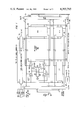
- FIG. 1 shows a memory having a second accessing pair of leads
- FIG. 2 shows a prior art memory having a single access pair
- FIG. 3 shows a timing chart for controlling the access between the dual ports of FIG. 1.
- the dual memory shown as gain value buffer 700, consists of an NMOS memory array of prior art (FIG. 2) modified to provide dual access capability.
- Memory 700 can be accessed either via register 703 or via register 704, each operating with two independent addresses and with two independent data buses.
- This structure is included in the illustrative embodiment of two concurrently filed copending patent applications, one of B. S. Moffitt, Ser. No. 256,970 and one of Baxter et al, Ser. No. 256,937, which applications are hereby incorporated by reference.
- the terminology used to identify the memory and the registers is the same as used in those applications to avoid confusion. It is to be understood that the dual memory which is the subject of our invention can be used in a wide range of applications.
- Bus 401 provides signals for read or write purposes and can access any of the 32 locations (0-31) selected by address decoder 705. Simultaneously, and independently, bus 707 can read out, if so desired, any of the 32 locations selected by address decoder 701. Both buses are extended as bit line pairs (for example, bit line pair 0, 0) through all of the memory locations and, as will be seen, access from either bus does not restrict access from the other bus. Bit line pairs are used as set/reset lines for write operations and as differential outputs for read operations as described prior. Bit line pair 0 1 and 0 1 of register 704 is extended to bit cells 702 of the top row (0-0 to 31-0) and bit line pair 0 and 0 of register 703 is also extended to these same cells.
- bit line pairs for example, bit line pair 0, 0
- any read or write operation is a two step process.
- the first step is to precharge all the bit line pairs. This precharging arrangement is well known. Thus, lines .0. to 5 and .0. to 5 are driven to a high state by circuits in the register 703. This prevents the lines from changing the data in the bit cells during the next step.
- the next step is to turn off the precharge drive and turn on one of the word select lines from the decoder 701.
- Turning off the precharge drive leaves the bit lines capacitively charged high, while the word select line turns on corresponding transmission gates 7021 and 7025.
- These transmission gates allow the bit cell to pull down one of the bit lines (.0. or .0. depending on the stored data) for each cell on the same column.
- Each bit line pair thus conforms to the data stored in the associated selected bit cell and the register then latches this data for output.
- bit cell resistors 7R1 and 7R2 are high value to minimize memory power consumption whereas transistors 7023 and 7024 are high power to be capable of pulling either bit line low.
- the precharge is required because the resistors are not capable of pulling the bit lines high.
- the next step is to replace the precharge drive with the drive of the input data, and turn on one of the select lines.
- the input data overrides the precharge and the bit cell data causing the cell data to be set or reset depending on the input data.
- the precharge and read/write operations are controlled by clock signals.
- the precharge is performed when clock is high and the read or write is performed when clock is low.
- the dual bus scheme allows a two phase operating memory system whereby two independent sets of I/O registers and word selectors can access all of the same memory cells on opposite phases of a clock signal.
- one of the registers such as input/output register 703 is in the precharge mode the actual flip-flop of the memory cell is isolated by gates 7021 and 7025 from that register's bit access lines.
- the other register such as output register 704, can be in the read/write phase actually accessing the same cell.
- This alternate operation is controlled by oppositely phased clock signals, provided by clock 102.
- the phase relationship between these signals is shown in FIG. 3. This phase difference prevents the potentially disasterous condition of having both bit lines simultaneously selecting the same bit cell.
- bus 707 is only used for read operations, but may also be used for both read and write operations, if so desired.
- the dual bit line/dual phase operation allows memory 700 to effectively double its speed so that twice as many accesses can occur through independent ports in the same time interval.
- This same dual phase arrangement can be further expanded by having three bit line pairs and three access ports and bus selection logic for two of the three access ports.
- Address selection logic for one output port can be shared between input/output registers. The other two ports are operable via separate registers. Addresses are simultaneously present to each register and on external bus selector controls when and from which bus data will be written into the memory.
- This arrangement provides a flexible three port memory system in which two ports are inputs and may perform simultaneous writes to more than one location and from either of two buses, while the third port is an output and provides simultaneous reads from a third bus. Since two ports are both running on the same clock phase this could create a conflict for writes except that the bus selection logic insures that for any given location only one bus will provide the write data at any one time. The third bus runs on the opposite phase and thus cannot conflict with either of the other two.
Abstract
Description
Claims (7)
Priority Applications (16)
| Application Number | Priority Date | Filing Date | Title |
|---|---|---|---|
| US06/256,697 US4395765A (en) | 1981-04-23 | 1981-04-23 | Multiport memory array |
| CA000400614A CA1173566A (en) | 1981-04-23 | 1982-04-07 | Multiport memory array |
| SE8202234A SE449672B (en) | 1981-04-23 | 1982-04-07 | MEMORY DEVICE, INCLUDING TWO PAIRS OF ACCESSORIES |
| GB8210963A GB2097623B (en) | 1981-04-23 | 1982-04-15 | Memory |
| DE3214230A DE3214230C2 (en) | 1981-04-23 | 1982-04-17 | Memory arrangement with multiple access lines |
| FR828206661A FR2504714B1 (en) | 1981-04-23 | 1982-04-19 | MULTIPLE ACCESS POINT MEMORY NETWORK |
| IL65529A IL65529A (en) | 1981-04-23 | 1982-04-19 | Multi-port memory array |
| NL8201680A NL192755C (en) | 1981-04-23 | 1982-04-22 | Memory system. |
| ES511598A ES511598A0 (en) | 1981-04-23 | 1982-04-22 | IMPROVEMENTS IN MEMORY SETS WITH MULTIPLE INPUTS. |
| BE0/207893A BE892929A (en) | 1981-04-23 | 1982-04-22 | MULTIPLE ACCESS POINT MEMORY NETWORK |
| IT20885/82A IT1150876B (en) | 1981-04-23 | 1982-04-22 | MULTI-PORT MEMORY MATRIX |
| AU82932/82A AU546325B2 (en) | 1981-04-23 | 1982-04-22 | Memory |
| IE949/82A IE53486B1 (en) | 1981-04-23 | 1982-04-22 | Memory |
| JP57067537A JPS57181493A (en) | 1981-04-23 | 1982-04-23 | Memory array |
| CH2490/82A CH654947A5 (en) | 1981-04-23 | 1982-04-23 | MEMORY ARRANGEMENT WITH A VARIETY OF MEMORY ELEMENTS. |
| HK70/86A HK7086A (en) | 1981-04-23 | 1986-01-30 | Memory |
Applications Claiming Priority (1)
| Application Number | Priority Date | Filing Date | Title |
|---|---|---|---|
| US06/256,697 US4395765A (en) | 1981-04-23 | 1981-04-23 | Multiport memory array |
Publications (1)
| Publication Number | Publication Date |
|---|---|
| US4395765A true US4395765A (en) | 1983-07-26 |
Family
ID=22973231
Family Applications (1)
| Application Number | Title | Priority Date | Filing Date |
|---|---|---|---|
| US06/256,697 Expired - Lifetime US4395765A (en) | 1981-04-23 | 1981-04-23 | Multiport memory array |
Country Status (16)
| Country | Link |
|---|---|
| US (1) | US4395765A (en) |
| JP (1) | JPS57181493A (en) |
| AU (1) | AU546325B2 (en) |
| BE (1) | BE892929A (en) |
| CA (1) | CA1173566A (en) |
| CH (1) | CH654947A5 (en) |
| DE (1) | DE3214230C2 (en) |
| ES (1) | ES511598A0 (en) |
| FR (1) | FR2504714B1 (en) |
| GB (1) | GB2097623B (en) |
| HK (1) | HK7086A (en) |
| IE (1) | IE53486B1 (en) |
| IL (1) | IL65529A (en) |
| IT (1) | IT1150876B (en) |
| NL (1) | NL192755C (en) |
| SE (1) | SE449672B (en) |
Cited By (10)
| Publication number | Priority date | Publication date | Assignee | Title |
|---|---|---|---|---|
| US4541076A (en) * | 1982-05-13 | 1985-09-10 | Storage Technology Corporation | Dual port CMOS random access memory |
| US4737933A (en) * | 1983-02-22 | 1988-04-12 | Storage Technology Partners | CMOS multiport general purpose register |
| EP0283223A2 (en) * | 1987-03-13 | 1988-09-21 | Brother Kogyo Kabushiki Kaisha | Memory unit |
| US4811300A (en) * | 1986-03-14 | 1989-03-07 | U.S. Philips Corporation | Memory device having a simplified sense amplifier with a buffer conductive during both precharge and read operations |
| US4995001A (en) * | 1988-10-31 | 1991-02-19 | International Business Machines Corporation | Memory cell and read circuit |
| US5150328A (en) * | 1988-10-25 | 1992-09-22 | Internation Business Machines Corporation | Memory organization with arrays having an alternate data port facility |
| US5166903A (en) * | 1988-10-25 | 1992-11-24 | International Business Machines Corporation | Memory organization with arrays having an alternate data port facility |
| US5235543A (en) * | 1989-12-29 | 1993-08-10 | Intel Corporation | Dual port static memory with one cycle read-modify-write |
| US5636176A (en) * | 1987-12-23 | 1997-06-03 | Texas Instruments Incorporated | Synchronous DRAM responsive to first and second clock signals |
| US5708850A (en) * | 1994-07-27 | 1998-01-13 | Sony Corporation | Parallel processing system for time division multiplex data transfer including read/write dual port memory accessible to bus and digital signal processor during opposite phases of clock |
Families Citing this family (2)
| Publication number | Priority date | Publication date | Assignee | Title |
|---|---|---|---|---|
| JPH0640439B2 (en) * | 1986-02-17 | 1994-05-25 | 日本電気株式会社 | Semiconductor memory device |
| DE3881222D1 (en) * | 1987-01-23 | 1993-07-01 | Siemens Ag | SEMICONDUCTOR MEMORY WITH OPTIONAL ACCESS THROUGH TWO SEPARATE INPUTS / OUTPUTS. |
Citations (7)
| Publication number | Priority date | Publication date | Assignee | Title |
|---|---|---|---|---|
| US3618050A (en) * | 1969-05-07 | 1971-11-02 | Teletype Corp | Read-only memory arrays in which a portion of the memory-addressing circuitry is integral to the array |
| US3636528A (en) * | 1969-11-14 | 1972-01-18 | Shell Oil Co | Half-bit memory cell array with nondestructive readout |
| US3916394A (en) * | 1974-12-09 | 1975-10-28 | Honeywell Inf Systems | High-speed random access memory |
| US3978459A (en) * | 1975-04-21 | 1976-08-31 | Intel Corporation | High density mos memory array |
| US4051358A (en) * | 1976-02-20 | 1977-09-27 | Intel Corporation | Apparatus and method for composing digital information on a data bus |
| US4125877A (en) * | 1976-11-26 | 1978-11-14 | Motorola, Inc. | Dual port random access memory storage cell |
| US4209851A (en) * | 1978-07-19 | 1980-06-24 | Texas Instruments Incorporated | Semiconductor memory cell with clocked voltage supply from data lines |
Family Cites Families (6)
| Publication number | Priority date | Publication date | Assignee | Title |
|---|---|---|---|---|
| US3866180A (en) * | 1973-04-02 | 1975-02-11 | Amdahl Corp | Having an instruction pipeline for concurrently processing a plurality of instructions |
| JPS52129337A (en) * | 1976-04-23 | 1977-10-29 | Hitachi Ltd | Memory circuit |
| US4104719A (en) * | 1976-05-20 | 1978-08-01 | The United States Of America As Represented By The Secretary Of The Navy | Multi-access memory module for data processing systems |
| US4123799A (en) * | 1977-09-19 | 1978-10-31 | Motorola, Inc. | High speed IFGET sense amplifier/latch |
| EP0011375A1 (en) * | 1978-11-17 | 1980-05-28 | Motorola, Inc. | Multi-port ram structure for data processor registers |
| JPS5634179A (en) * | 1979-08-24 | 1981-04-06 | Mitsubishi Electric Corp | Control circuit for memory unit |
-
1981
- 1981-04-23 US US06/256,697 patent/US4395765A/en not_active Expired - Lifetime
-
1982
- 1982-04-07 CA CA000400614A patent/CA1173566A/en not_active Expired
- 1982-04-07 SE SE8202234A patent/SE449672B/en not_active IP Right Cessation
- 1982-04-15 GB GB8210963A patent/GB2097623B/en not_active Expired
- 1982-04-17 DE DE3214230A patent/DE3214230C2/en not_active Expired - Fee Related
- 1982-04-19 FR FR828206661A patent/FR2504714B1/en not_active Expired
- 1982-04-19 IL IL65529A patent/IL65529A/en unknown
- 1982-04-22 NL NL8201680A patent/NL192755C/en not_active IP Right Cessation
- 1982-04-22 ES ES511598A patent/ES511598A0/en active Granted
- 1982-04-22 IT IT20885/82A patent/IT1150876B/en active
- 1982-04-22 AU AU82932/82A patent/AU546325B2/en not_active Ceased
- 1982-04-22 IE IE949/82A patent/IE53486B1/en unknown
- 1982-04-22 BE BE0/207893A patent/BE892929A/en not_active IP Right Cessation
- 1982-04-23 CH CH2490/82A patent/CH654947A5/en not_active IP Right Cessation
- 1982-04-23 JP JP57067537A patent/JPS57181493A/en active Pending
-
1986
- 1986-01-30 HK HK70/86A patent/HK7086A/en not_active IP Right Cessation
Patent Citations (7)
| Publication number | Priority date | Publication date | Assignee | Title |
|---|---|---|---|---|
| US3618050A (en) * | 1969-05-07 | 1971-11-02 | Teletype Corp | Read-only memory arrays in which a portion of the memory-addressing circuitry is integral to the array |
| US3636528A (en) * | 1969-11-14 | 1972-01-18 | Shell Oil Co | Half-bit memory cell array with nondestructive readout |
| US3916394A (en) * | 1974-12-09 | 1975-10-28 | Honeywell Inf Systems | High-speed random access memory |
| US3978459A (en) * | 1975-04-21 | 1976-08-31 | Intel Corporation | High density mos memory array |
| US4051358A (en) * | 1976-02-20 | 1977-09-27 | Intel Corporation | Apparatus and method for composing digital information on a data bus |
| US4125877A (en) * | 1976-11-26 | 1978-11-14 | Motorola, Inc. | Dual port random access memory storage cell |
| US4209851A (en) * | 1978-07-19 | 1980-06-24 | Texas Instruments Incorporated | Semiconductor memory cell with clocked voltage supply from data lines |
Non-Patent Citations (3)
| Title |
|---|
| "Telephony and Signal Processing", Chapter 4, Intel Corp., 1980, pp. 4-4-16. * |
| E. Douglas Jensen, "Mixed Mode and Multidimensional Memories", IEEE Catalog No. 72CH0659-3C, Sep. 1972, pp. 119-121. * |
| Teuvo Kohonen, "Associative Memory", Springer-Verlag, 1977, pp. 64-65. * |
Cited By (11)
| Publication number | Priority date | Publication date | Assignee | Title |
|---|---|---|---|---|
| US4541076A (en) * | 1982-05-13 | 1985-09-10 | Storage Technology Corporation | Dual port CMOS random access memory |
| US4737933A (en) * | 1983-02-22 | 1988-04-12 | Storage Technology Partners | CMOS multiport general purpose register |
| US4811300A (en) * | 1986-03-14 | 1989-03-07 | U.S. Philips Corporation | Memory device having a simplified sense amplifier with a buffer conductive during both precharge and read operations |
| EP0283223A2 (en) * | 1987-03-13 | 1988-09-21 | Brother Kogyo Kabushiki Kaisha | Memory unit |
| EP0283223A3 (en) * | 1987-03-13 | 1990-01-10 | Brother Kogyo Kabushiki Kaisha | Memory unit |
| US5636176A (en) * | 1987-12-23 | 1997-06-03 | Texas Instruments Incorporated | Synchronous DRAM responsive to first and second clock signals |
| US5150328A (en) * | 1988-10-25 | 1992-09-22 | Internation Business Machines Corporation | Memory organization with arrays having an alternate data port facility |
| US5166903A (en) * | 1988-10-25 | 1992-11-24 | International Business Machines Corporation | Memory organization with arrays having an alternate data port facility |
| US4995001A (en) * | 1988-10-31 | 1991-02-19 | International Business Machines Corporation | Memory cell and read circuit |
| US5235543A (en) * | 1989-12-29 | 1993-08-10 | Intel Corporation | Dual port static memory with one cycle read-modify-write |
| US5708850A (en) * | 1994-07-27 | 1998-01-13 | Sony Corporation | Parallel processing system for time division multiplex data transfer including read/write dual port memory accessible to bus and digital signal processor during opposite phases of clock |
Also Published As
| Publication number | Publication date |
|---|---|
| SE449672B (en) | 1987-05-11 |
| AU546325B2 (en) | 1985-08-29 |
| IE53486B1 (en) | 1988-11-23 |
| BE892929A (en) | 1982-08-16 |
| HK7086A (en) | 1986-02-07 |
| CA1173566A (en) | 1984-08-28 |
| IL65529A0 (en) | 1982-07-30 |
| GB2097623B (en) | 1984-09-26 |
| ES8302945A1 (en) | 1983-02-16 |
| GB2097623A (en) | 1982-11-03 |
| FR2504714A1 (en) | 1982-10-29 |
| JPS57181493A (en) | 1982-11-08 |
| ES511598A0 (en) | 1983-02-16 |
| DE3214230A1 (en) | 1982-11-18 |
| NL8201680A (en) | 1982-11-16 |
| IE820949L (en) | 1982-10-23 |
| SE8202234L (en) | 1982-10-24 |
| DE3214230C2 (en) | 1994-01-13 |
| NL192755B (en) | 1997-09-01 |
| FR2504714B1 (en) | 1989-04-28 |
| AU8293282A (en) | 1982-10-28 |
| IT1150876B (en) | 1986-12-17 |
| IT8220885A0 (en) | 1982-04-22 |
| CH654947A5 (en) | 1986-03-14 |
| NL192755C (en) | 1998-01-06 |
| IL65529A (en) | 1985-05-31 |
Similar Documents
| Publication | Publication Date | Title |
|---|---|---|
| KR940000148B1 (en) | Dual port semiconductor memory device | |
| US5568428A (en) | Memory device and serial-parallel data transform circuit | |
| EP0188059B1 (en) | Semiconductor memory device having read-modify-write configuration | |
| JP2740063B2 (en) | Semiconductor storage device | |
| JP2683919B2 (en) | Semiconductor memory device | |
| EP0675500B1 (en) | An improved memory device and method of construction | |
| US4395765A (en) | Multiport memory array | |
| JPH0255878B2 (en) | ||
| EP0121726A2 (en) | Multi-port memory cell and system | |
| JPS61160898A (en) | Semiconductor memory device | |
| JPH0760594B2 (en) | Semiconductor memory device | |
| JPH01184693A (en) | Semiconductor memory | |
| US6175533B1 (en) | Multi-port memory cell with preset | |
| US5826056A (en) | Synchronous memory device and method of reading data from same | |
| US4811305A (en) | Semiconductor memory having high-speed serial access scheme | |
| EP0570977A2 (en) | Semiconductor memory device | |
| KR20000013391A (en) | Data transmission circuit in a synchronous semiconductor memory device | |
| JP2845187B2 (en) | Semiconductor storage device | |
| US6021084A (en) | Multi-bit block write in a random access memory | |
| US5896339A (en) | Multi-bit block write in a random access memory | |
| KR100334574B1 (en) | Burst-type semiconductor memory device having full-page mode | |
| US5521877A (en) | Serial random access memory device capable of reducing peak current through subword data register | |
| JPS623504B2 (en) | ||
| US6442097B2 (en) | Virtual channel DRAM | |
| KR100301802B1 (en) | Semiconductor memory device |
Legal Events
| Date | Code | Title | Description |
|---|---|---|---|
| AS | Assignment |
Owner name: BELL TELEPHONE LABORATORIES,INCORPORATED,600 MOUNT Free format text: ASSIGNMENT OF ASSIGNORS INTEREST.;ASSIGNORS:MOFFITT BRYAN S.;ROSS ALEXANDER R.;REEL/FRAME:003881/0168 Effective date: 19810420 Owner name: BELL TELEPHONE LABORATORIES, INCORPORATED, A CORP. Free format text: ASSIGNMENT OF ASSIGNORS INTEREST;ASSIGNORS:MOFFITT BRYAN S.;ROSS ALEXANDER R.;REEL/FRAME:003881/0168 Effective date: 19810420 |
|
| STCF | Information on status: patent grant |
Free format text: PATENTED CASE |
|
| MAFP | Maintenance fee payment |
Free format text: PAYMENT OF MAINTENANCE FEE, 4TH YEAR, PL 96-517 (ORIGINAL EVENT CODE: M170); ENTITY STATUS OF PATENT OWNER: LARGE ENTITY Year of fee payment: 4 |
|
| FEPP | Fee payment procedure |
Free format text: PAYOR NUMBER ASSIGNED (ORIGINAL EVENT CODE: ASPN); ENTITY STATUS OF PATENT OWNER: LARGE ENTITY |
|
| MAFP | Maintenance fee payment |
Free format text: PAYMENT OF MAINTENANCE FEE, 8TH YEAR, PL 96-517 (ORIGINAL EVENT CODE: M171); ENTITY STATUS OF PATENT OWNER: LARGE ENTITY Year of fee payment: 8 |
|
| MAFP | Maintenance fee payment |
Free format text: PAYMENT OF MAINTENANCE FEE, 12TH YEAR, LARGE ENTITY (ORIGINAL EVENT CODE: M185); ENTITY STATUS OF PATENT OWNER: LARGE ENTITY Year of fee payment: 12 |