US4355334A - Dimmer and dimmer override control for a display device - Google Patents
Dimmer and dimmer override control for a display device Download PDFInfo
- Publication number
- US4355334A US4355334A US06/268,441 US26844181A US4355334A US 4355334 A US4355334 A US 4355334A US 26844181 A US26844181 A US 26844181A US 4355334 A US4355334 A US 4355334A
- Authority
- US
- United States
- Prior art keywords
- dimmer
- transistor
- video signal
- signal
- base
- Prior art date
- Legal status (The legal status is an assumption and is not a legal conclusion. Google has not performed a legal analysis and makes no representation as to the accuracy of the status listed.)
- Expired - Fee Related
Links
Images
Classifications
-
- H—ELECTRICITY
- H04—ELECTRIC COMMUNICATION TECHNIQUE
- H04N—PICTORIAL COMMUNICATION, e.g. TELEVISION
- H04N5/00—Details of television systems
- H04N5/44—Receiver circuitry for the reception of television signals according to analogue transmission standards
- H04N5/57—Control of contrast or brightness
- H04N5/58—Control of contrast or brightness in dependence upon ambient light
Definitions
- This invention is directed to an improved dimmer control and dimmer override for use with a display device such as a CRT (cathode ray tube).
- a display device such as a CRT (cathode ray tube).
- CRTs are frequently used to display graphics and other types of video under ambient light conditions which can vary greaty. Accordingly, it is helpful if the CRT is controlled by a dimmer so that image brightness is increased as the intensity of ambient light increases. When the intensity of ambient light decreases, the brightness of the image may be correspondingly decreased.
- the CRT image be at maximum brightness, irrespective of ambient light conditions.
- a bright image is desired to ensure that the emergency message is easily readable.
- This override of the dimming function also helps to highlight the emergency message so it is more easily distinguished from a routine message.
- CRT controls which provide the functions described above is that they be simple, reliable, and inexpensive, particularly for high volume consumer applications.
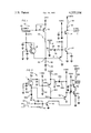
- FIG. 1 is a schematic diagram of a dimmer and dimmer override control embodying various aspects of the invention.
- FIG. 2 is a schematic diagram of another embodiment of the invention.
- a dimmer and dimmer override control 10 is shown for use in controlling the amplitude of a video signal applied to a CRT (not shown) or any other type of display device.
- an input video signal is applied to a terminal 12 and an amplified video signal is developed at an output terminal 14.
- the amplitude of the video signal at terminal 14 is controlled by a light sensor 16 and a video clipping transistor 18. Override of the clipping function is provided by another transistor 20.
- the illustrated embodiment includes a cascode amplifier comprising an input transistor 22 whose base receives the video signal via a resistor 24 and a diode 26.
- the diode may be connected to the wiper arm 28 of a variable resistor 30 to set the video level at the output terminal 14.
- the collector of the transistor 22 couples to the emitter of an output transistor 32 whose collector is coupled to a resistor 34, a coil 36 and the output terminal 14.
- the sensor 16 (a light sensitive transistor, for example) is situated so as to receive ambient light indicated at 38, and to develop a dimmer control signal at a node 40 for varying the bias on the transistor 18.
- the sensor 16 conducts harder to raise the potential at the node 40.
- Suitable biasing resistors and filter capacitors may be coupled to the base and collector of the sensor 16 as shown to establish a selected operating condition for the sensor.
- the clipping transistor 18 may be of the PNP type with its collector grounded, its emitter coupled to the base of the transistor 22, and its base coupled to the node 40.
- a resistor 42 and a diode 44 may be coupled between ground and the node 40.
- the transistor 18 is non-conductive in the absence of a video signal.
- the sensor 16 develops a relatively high positive voltage at the node 40. This reverse biases the transistor 18 so that video signals at the base of transistor 22 cannot turn on the transistor 18.
- those video signals do not become clipped and appear at a relatively large amplitude at the terminal 14.
- the amplitude of the control signal developed by sensor 16 decreases. Consequently, the reverse bias on transistor 18 is removed so that the relatively large amplitude video signals at the base of transistor 22 now turn on the transistor 18. Hence, they are clipped and a reduced amplitude video output is developed to produce a dimmer image.
- large amplitude video signals may be clipped at their tips, but less clipping occurs than during higher level lighting conditions. It can be seen, therefore, that the clipping level of the transistor 18 varies according to ambient light conditions.
- the video input at terminal 12 corresponds to an emergency or warning message
- its amplitude is automatically raised conventionally by a video generator.
- the collector of transistor 20 is coupled via a resistor 46 to the node 40
- its emitter is coupled to a voltage source
- its base is coupled to a terminal 48 via a resistor 49 for receiving a dimmer override signal.
- the dimmer override signal may be an open collector pull down which occurs concurrently with a large amplitude video warning signal.
- the transistor 20 In response to the dimmer override signal, the transistor 20 conducts to raise the voltage at node 40 to reverse bias the transistor 18 so that it cannot be turned on by large amplitude video signals at the base of transistor 22. Consequently, the clipping function is defeated, and a large amplitude video warning signal appears at terminal 14.
- the CRT may display emergency and non-emergency messages or graphics concurrently.
- the dimmer override function only operates on an emergency message.
- the emergency message appears as the brighter of the two messages and, therefore, easily directs a viewer's attention to it.
- FIG. 2 components thereof which correspond to similarly functioning components of FIG. 1 have the same reference numeral followed by the character "A".
- the video amplifier and the light sensor are identical to those shown in FIG. 1.
- a major difference between the controls 10A and 10 is that the former is adapted to use the video signal itself as the dimmer override signal.
- the emitter of the transistor 20A is coupled to the video input terminal 12A and its base is coupled to a DC potential established by resistors 50 and 51.
- a resistor 46A couples the collector of transistor 20A to node 40A.
- Non-emergency video signals at terminal 12A may have an amplitude of 2 volts, for example.
- Emergency video signals may have an amplitude of about 4 volts.
- the DC potential at the base of the transistor 20 is selected to hold the transistor 20A off when the non-emergency video signals arrive, and to turn the transistor 20A on when the larger amplitude emergency video signals arrive.
- the transistor 20A conducts to raise the potential of node 40A for biasing the transistor 18A to a level which permits maximum brightness to be obtained without saturating the amplifier.
- the clipping action of transistor 18A is controlled to provide a maximum video output, and the emergency video is output at terminal 14A at a large amplitude.
- the transistor 20A acts as a comparator to distinguish between emergency and non-emergency signals.
- Horizontal rate pulses 54 may be coupled to the base of transistor 52 via an R-C network 56 and vertical rate pulses 58 may be coupled to its base via a resistor 60.
- the collector of transistor 52 may be coupled to the base of transistor 22A to turn it off in the presence of the horizontal and vertical rate pulses.
- Similar circuitry may be coupled to the base of transistor 22 (FIG. 1) to blank the amplifier in the control 10.
- the dimmer and override controls are relatively simple and inexpensive. Consequently, they may be used in high volume consumer applications such as displays which show the operating characteristics of vehicles. Many other such applications will be apparent.
Abstract
Description
Claims (8)
Priority Applications (1)
| Application Number | Priority Date | Filing Date | Title |
|---|---|---|---|
| US06/268,441 US4355334A (en) | 1981-05-29 | 1981-05-29 | Dimmer and dimmer override control for a display device |
Applications Claiming Priority (1)
| Application Number | Priority Date | Filing Date | Title |
|---|---|---|---|
| US06/268,441 US4355334A (en) | 1981-05-29 | 1981-05-29 | Dimmer and dimmer override control for a display device |
Publications (1)
| Publication Number | Publication Date |
|---|---|
| US4355334A true US4355334A (en) | 1982-10-19 |
Family
ID=23023020
Family Applications (1)
| Application Number | Title | Priority Date | Filing Date |
|---|---|---|---|
| US06/268,441 Expired - Fee Related US4355334A (en) | 1981-05-29 | 1981-05-29 | Dimmer and dimmer override control for a display device |
Country Status (1)
| Country | Link |
|---|---|
| US (1) | US4355334A (en) |
Cited By (22)
| Publication number | Priority date | Publication date | Assignee | Title |
|---|---|---|---|---|
| US4698681A (en) * | 1985-09-11 | 1987-10-06 | Zenith Electronics Corporation | Dual intensity video circuit |
| GB2233530A (en) * | 1989-05-17 | 1991-01-09 | Fuji Heavy Ind Ltd | System for controlling a video display system of a motor vehicle |
| US5534920A (en) * | 1993-07-14 | 1996-07-09 | Samsung Electronics Co., Ltd. | Viewfinder brightness control circuit for a camcorder employing iris output voltage and method therefor |
| US5734439A (en) * | 1995-03-10 | 1998-03-31 | Alcatel N.V. | Circuit arrangement for indicating ambient light conditions of a video pickup and video display device |
| US5847773A (en) * | 1991-08-30 | 1998-12-08 | Thomson Consumer Electronics, Inc. | Video system including apparatus for deactivating an automatic control arrangement |
| US6710763B1 (en) | 1999-08-31 | 2004-03-23 | Matsushita Electric Industrial Co., Ltd. | Display control method and display controller |
| US20040070565A1 (en) * | 2001-12-05 | 2004-04-15 | Nayar Shree K | Method and apparatus for displaying images |
| US20050134599A1 (en) * | 2003-07-02 | 2005-06-23 | Shree Nayar | Methods and systems for compensating an image projected onto a surface having spatially varying photometric properties |
| US20070257928A1 (en) * | 2006-05-04 | 2007-11-08 | Richard Marks | Bandwidth Management Through Lighting Control of a User Environment via a Display Device |
| US20070279427A1 (en) * | 2006-05-04 | 2007-12-06 | Richard Marks | Lighting Control of a User Environment via a Display Device |
| US20080309754A1 (en) * | 2004-10-25 | 2008-12-18 | Columbia University | Systems and Methods for Displaying Three-Dimensional Images |
| US8133115B2 (en) | 2003-10-22 | 2012-03-13 | Sony Computer Entertainment America Llc | System and method for recording and displaying a graphical path in a video game |
| US8284310B2 (en) | 2005-06-22 | 2012-10-09 | Sony Computer Entertainment America Llc | Delay matching in audio/video systems |
| US8289325B2 (en) | 2004-10-06 | 2012-10-16 | Sony Computer Entertainment America Llc | Multi-pass shading |
| US20130100150A1 (en) * | 2010-03-25 | 2013-04-25 | Nokia Corporation | Apparatus, Display Module and Method for Adaptive Blank Frame Insertion |
| US9108108B2 (en) | 2007-09-05 | 2015-08-18 | Sony Computer Entertainment America Llc | Real-time, contextual display of ranked, user-generated game play advice |
| US9126116B2 (en) | 2007-09-05 | 2015-09-08 | Sony Computer Entertainment America Llc | Ranking of user-generated game play advice |
| US9342817B2 (en) | 2011-07-07 | 2016-05-17 | Sony Interactive Entertainment LLC | Auto-creating groups for sharing photos |
| US9833707B2 (en) | 2012-10-29 | 2017-12-05 | Sony Interactive Entertainment Inc. | Ambient light control and calibration via a console |
| US10128914B1 (en) | 2017-09-06 | 2018-11-13 | Sony Interactive Entertainment LLC | Smart tags with multiple interactions |
| US10561942B2 (en) | 2017-05-15 | 2020-02-18 | Sony Interactive Entertainment America Llc | Metronome for competitive gaming headset |
| US10786736B2 (en) | 2010-05-11 | 2020-09-29 | Sony Interactive Entertainment LLC | Placement of user information in a game space |
Citations (1)
| Publication number | Priority date | Publication date | Assignee | Title |
|---|---|---|---|---|
| JPS5221724A (en) * | 1975-08-12 | 1977-02-18 | Sony Corp | Automatic brightness adjusting circuit |
-
1981
- 1981-05-29 US US06/268,441 patent/US4355334A/en not_active Expired - Fee Related
Patent Citations (1)
| Publication number | Priority date | Publication date | Assignee | Title |
|---|---|---|---|---|
| JPS5221724A (en) * | 1975-08-12 | 1977-02-18 | Sony Corp | Automatic brightness adjusting circuit |
Cited By (33)
| Publication number | Priority date | Publication date | Assignee | Title |
|---|---|---|---|---|
| US4698681A (en) * | 1985-09-11 | 1987-10-06 | Zenith Electronics Corporation | Dual intensity video circuit |
| GB2233530A (en) * | 1989-05-17 | 1991-01-09 | Fuji Heavy Ind Ltd | System for controlling a video display system of a motor vehicle |
| US5847773A (en) * | 1991-08-30 | 1998-12-08 | Thomson Consumer Electronics, Inc. | Video system including apparatus for deactivating an automatic control arrangement |
| US5534920A (en) * | 1993-07-14 | 1996-07-09 | Samsung Electronics Co., Ltd. | Viewfinder brightness control circuit for a camcorder employing iris output voltage and method therefor |
| US5734439A (en) * | 1995-03-10 | 1998-03-31 | Alcatel N.V. | Circuit arrangement for indicating ambient light conditions of a video pickup and video display device |
| US6710763B1 (en) | 1999-08-31 | 2004-03-23 | Matsushita Electric Industrial Co., Ltd. | Display control method and display controller |
| US20040070565A1 (en) * | 2001-12-05 | 2004-04-15 | Nayar Shree K | Method and apparatus for displaying images |
| US20050134599A1 (en) * | 2003-07-02 | 2005-06-23 | Shree Nayar | Methods and systems for compensating an image projected onto a surface having spatially varying photometric properties |
| US7663640B2 (en) | 2003-07-02 | 2010-02-16 | The Trustees Of Columbia University In The City Of New York | Methods and systems for compensating an image projected onto a surface having spatially varying photometric properties |
| US8133115B2 (en) | 2003-10-22 | 2012-03-13 | Sony Computer Entertainment America Llc | System and method for recording and displaying a graphical path in a video game |
| US8289325B2 (en) | 2004-10-06 | 2012-10-16 | Sony Computer Entertainment America Llc | Multi-pass shading |
| US20080309754A1 (en) * | 2004-10-25 | 2008-12-18 | Columbia University | Systems and Methods for Displaying Three-Dimensional Images |
| US7703924B2 (en) | 2004-10-25 | 2010-04-27 | The Trustees Of Columbia University In The City Of New York | Systems and methods for displaying three-dimensional images |
| US8284310B2 (en) | 2005-06-22 | 2012-10-09 | Sony Computer Entertainment America Llc | Delay matching in audio/video systems |
| US8204272B2 (en) | 2006-05-04 | 2012-06-19 | Sony Computer Entertainment Inc. | Lighting control of a user environment via a display device |
| US7965859B2 (en) | 2006-05-04 | 2011-06-21 | Sony Computer Entertainment Inc. | Lighting control of a user environment via a display device |
| US7880746B2 (en) | 2006-05-04 | 2011-02-01 | Sony Computer Entertainment Inc. | Bandwidth management through lighting control of a user environment via a display device |
| US8243089B2 (en) | 2006-05-04 | 2012-08-14 | Sony Computer Entertainment Inc. | Implementing lighting control of a user environment |
| US20070279427A1 (en) * | 2006-05-04 | 2007-12-06 | Richard Marks | Lighting Control of a User Environment via a Display Device |
| US20070257928A1 (en) * | 2006-05-04 | 2007-11-08 | Richard Marks | Bandwidth Management Through Lighting Control of a User Environment via a Display Device |
| US10486069B2 (en) | 2007-09-05 | 2019-11-26 | Sony Interactive Entertainment America Llc | Ranking of user-generated game play advice |
| US9108108B2 (en) | 2007-09-05 | 2015-08-18 | Sony Computer Entertainment America Llc | Real-time, contextual display of ranked, user-generated game play advice |
| US9126116B2 (en) | 2007-09-05 | 2015-09-08 | Sony Computer Entertainment America Llc | Ranking of user-generated game play advice |
| US20130100150A1 (en) * | 2010-03-25 | 2013-04-25 | Nokia Corporation | Apparatus, Display Module and Method for Adaptive Blank Frame Insertion |
| US10991338B2 (en) * | 2010-03-25 | 2021-04-27 | Nokia Technologies Oy | Apparatus, display module and method for adaptive blank frame insertion |
| US10786736B2 (en) | 2010-05-11 | 2020-09-29 | Sony Interactive Entertainment LLC | Placement of user information in a game space |
| US11478706B2 (en) | 2010-05-11 | 2022-10-25 | Sony Interactive Entertainment LLC | Placement of user information in a game space |
| US9342817B2 (en) | 2011-07-07 | 2016-05-17 | Sony Interactive Entertainment LLC | Auto-creating groups for sharing photos |
| US9833707B2 (en) | 2012-10-29 | 2017-12-05 | Sony Interactive Entertainment Inc. | Ambient light control and calibration via a console |
| US9950259B2 (en) | 2012-10-29 | 2018-04-24 | Sony Interactive Entertainment Inc. | Ambient light control and calibration via a console |
| US10561942B2 (en) | 2017-05-15 | 2020-02-18 | Sony Interactive Entertainment America Llc | Metronome for competitive gaming headset |
| US10128914B1 (en) | 2017-09-06 | 2018-11-13 | Sony Interactive Entertainment LLC | Smart tags with multiple interactions |
| US10541731B2 (en) | 2017-09-06 | 2020-01-21 | Sony Interactive Entertainment LLC | Smart tags with multiple interactions |
Similar Documents
| Publication | Publication Date | Title |
|---|---|---|
| US4355334A (en) | Dimmer and dimmer override control for a display device | |
| US4451849A (en) | Plural operating mode ambient light responsive television picture control | |
| KR910005675A (en) | TV system | |
| US4298884A (en) | Chroma amplifier and color killer | |
| RU2130235C1 (en) | Device for regulation of brightness and contrast in tv set | |
| CA1154152A (en) | Video signal processing circuit | |
| KR870011793A (en) | Video Signal Processing and Display System | |
| US6563495B1 (en) | Automatic screen saver | |
| EP1042910B1 (en) | Automatic screen saver | |
| EP0574711A1 (en) | Automatic contrast control circuit with inserted vertical blanking | |
| US4760450A (en) | Limiter circuit for preventing blooming in a video display terminal | |
| KR840003183A (en) | Automatic brightness limit circuit | |
| KR840006739A (en) | Auto Bias Adjuster | |
| US4414574A (en) | Video amplifier with blank stretching | |
| KR870008479A (en) | Video signal processing system | |
| KR0130174Y1 (en) | Auto-cutoff compensation circuit | |
| JPS6128226Y2 (en) | ||
| KR910004793Y1 (en) | Automatic beam control circuit | |
| JP2537959B2 (en) | Video signal amplitude limiter | |
| KR910005804Y1 (en) | Frequency compensation circuit | |
| JP2516098B2 (en) | Image display device | |
| JPH066725A (en) | Contrast control circuit | |
| KR900000776Y1 (en) | Speed up devices of beam current auto-control circuits | |
| KR960001256Y1 (en) | Automatic control device of color gain | |
| JP2599334B2 (en) | Limiter circuit |
Legal Events
| Date | Code | Title | Description |
|---|---|---|---|
| AS | Assignment |
Owner name: ZENITH RADIO CORPORATION, 1000 MILWAUKEE AVENUE, G Free format text: ASSIGNMENT OF ASSIGNORS INTEREST.;ASSIGNORS:FITZGIBBON, JAMES J.;SUTTON, LEROY;REEL/FRAME:004020/0896 Effective date: 19810626 Owner name: ZENITH RADIO CORPORATION, A CORP. OF DE, ILLINOIS Free format text: ASSIGNMENT OF ASSIGNORS INTEREST;ASSIGNORS:FITZGIBBON, JAMES J.;SUTTON, LEROY;REEL/FRAME:004020/0896 Effective date: 19810626 |
|
| MAFP | Maintenance fee payment |
Free format text: PAYMENT OF MAINTENANCE FEE, 4TH YEAR, PL 96-517 (ORIGINAL EVENT CODE: M170); ENTITY STATUS OF PATENT OWNER: LARGE ENTITY Year of fee payment: 4 |
|
| MAFP | Maintenance fee payment |
Free format text: PAYMENT OF MAINTENANCE FEE, 8TH YEAR, PL 96-517 (ORIGINAL EVENT CODE: M171); ENTITY STATUS OF PATENT OWNER: LARGE ENTITY Year of fee payment: 8 |
|
| AS | Assignment |
Owner name: FIRST NATIONAL BANK OF CHICAGO, THE Free format text: SECURITY INTEREST;ASSIGNOR:ZENITH ELECTRONICS CORPORATION A CORP. OF DELAWARE;REEL/FRAME:006187/0650 Effective date: 19920619 |
|
| AS | Assignment |
Owner name: ZENITH ELECTRONICS CORPORATION Free format text: RELEASED BY SECURED PARTY;ASSIGNOR:FIRST NATIONAL BANK OF CHICAGO, THE (AS COLLATERAL AGENT).;REEL/FRAME:006243/0013 Effective date: 19920827 |
|
| FEPP | Fee payment procedure |
Free format text: MAINTENANCE FEE REMINDER MAILED (ORIGINAL EVENT CODE: REM.); ENTITY STATUS OF PATENT OWNER: LARGE ENTITY |
|
| LAPS | Lapse for failure to pay maintenance fees | ||
| FP | Lapsed due to failure to pay maintenance fee |
Effective date: 19941019 |
|
| STCH | Information on status: patent discontinuation |
Free format text: PATENT EXPIRED DUE TO NONPAYMENT OF MAINTENANCE FEES UNDER 37 CFR 1.362 |