US4348762A - Circuit for correcting data reading clock pulses - Google Patents
Circuit for correcting data reading clock pulses Download PDFInfo
- Publication number
- US4348762A US4348762A US06/176,974 US17697480A US4348762A US 4348762 A US4348762 A US 4348762A US 17697480 A US17697480 A US 17697480A US 4348762 A US4348762 A US 4348762A
- Authority
- US
- United States
- Prior art keywords
- clock pulses
- reading
- groups
- data
- mis
- Prior art date
- Legal status (The legal status is an assumption and is not a legal conclusion. Google has not performed a legal analysis and makes no representation as to the accuracy of the status listed.)
- Expired - Lifetime
Links
Images
Classifications
-
- H—ELECTRICITY
- H04—ELECTRIC COMMUNICATION TECHNIQUE
- H04L—TRANSMISSION OF DIGITAL INFORMATION, e.g. TELEGRAPHIC COMMUNICATION
- H04L7/00—Arrangements for synchronising receiver with transmitter
- H04L7/02—Speed or phase control by the received code signals, the signals containing no special synchronisation information
- H04L7/033—Speed or phase control by the received code signals, the signals containing no special synchronisation information using the transitions of the received signal to control the phase of the synchronising-signal-generating means, e.g. using a phase-locked loop
- H04L7/0337—Selecting between two or more discretely delayed clocks or selecting between two or more discretely delayed received code signals
Definitions
- This invention relates to a circuit for correcting data reading clock pulses, and more particularly to an improved circuit for correcting data reading clock pulses which is capable of eliminating mis-reading of data due to timing error of the data reading clock pulses.
- reading clock pulses are required to read n-bits of data within a period of time T and the timing of the pulses must be synchronized with an external signal.
- a synchronizing signal is generally required.
- a start bit is formed, as dummy data, in the data to be read, so as to act as the desired synchronizing signal.
- a circuit for correlating data reading clock pulses including a clock pulse generator for generating a plurality of groups of clock pulses different in phases, a switch for selecting and outputting one or more groups of clock pulses from the plurality of groups of clock pulses, a device for reading data in response to one or more groups of clock pulses selected by the switch, a detector for detecting mis-reading of the data and outputting a detection signal, and a switch control responsive to the detection signal to control the switch so as to continue selection of another group or groups of clock pulses until correct data reading is accomplished.
- FIG. 1 is a block diagram of one form of a circuit for correcting data reading clock pulses in accordance with the present invention
- FIG. 2 is a block diagram of one specific form of a principal portion of the circuit illustrated in FIG. 1;
- FIG. 3 shows IC 1 and IC 2 of FIG. 2;
- FIG. 4 shows one of the switch circuits S 1 -S 8 of FIG. 3;
- FIG. 5 shows IC 3 of FIG. 2.
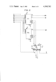
- numeral 1 designates a data reading device such as a known tape reader.
- Numeral 2 is a detector for detecting misreading of data
- 3 is a switch control circuit
- SW 1 to SW n are switches
- 4 is a clock pulse generator for generating clock pulses of groups ⁇ 1 to ⁇ n of n different phases each generally synchronized with a desired external signal.
- a time of one data bit is divided into n parts to form the clock pulse groups ⁇ 1 to ⁇ n of n phases.
- Out of these clock pulse groups ⁇ 1 to ⁇ n a given number of clock pulse groups or groups are selected by corresponding switches SW 1 to SW n closed by the switch control circuit 3.
- one clock pulse group is selected and the selected clock pulse ⁇ out is outputted to the data reading device 1.
- the detector detects the error and the switch control circuit 3 is actuated by the detection signal so that the switch in a closed position is opened and another switch is closed to select another clock pulse group.
- the switch control circuit 3 automatically goes on scanning of the switches, closing the switches sequentially, in response to the detection signals of mis-reading of the data, until a clock pulse ⁇ out desired for accurate data reading is obtained.
- the detector 2 may be a known detector which is adapted to detect an error through an output of a parity check or continuous-transmission check of the read-out data.
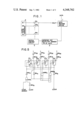
- FIG. 2 illustrates one example of an arrangement of the switches SW and the switch control circuit 3 employing IC circuits.
- IC 1 and IC 2 are analog switch circuits and have functions equivalent to those of the switches SW 1 to SW n .
- the circuit IC 1 receives input clock pulses ⁇ 2 to ⁇ 7 and selectively outputs one of the clock pulses ⁇ 2 to ⁇ 5 to an output ⁇ 8 and outputs one of the clock pulses ⁇ 3 to ⁇ 6 to an output ⁇ 1 .
- the circuit IC 2 receives inputs ⁇ 4 to ⁇ 7 and outputs one of the clock pulses ⁇ 4 to ⁇ 7 to an output ⁇ 2 .
- IC 3 is a counter having a function of the switch control circuit 3 as mentioned above.
- An input terminal I 2 of the counter IC 3 receives a detection output (for example "0" for mis-reading and "1" for correct reading) from the detector 2, while an input terminal I 1 receives a clock pulse ⁇ 8 .
- I 3 is a reset terminal.
- O 1 and O 2 are output terminals and connected to control terminals C 1 and C 2 of the analog switch circuit, respectively.
- Numerals indicated around the respective IC circuit IC 1 to IC 3 designate terminal numbers of IC chips of the respective circuits.
- the detection output "0" is applied to the input terminal I 2 of the counter IC 3 and the counter IC 3 starts to count the clock pulses ⁇ 8 in response to the detection output. If the mis-reading remains uncorrected, for example, after eight clock pulses have been counted, i.e., the data reading device has failed to correctly read the data eight times, level conditions of the output terminals 01 and 02 are changed and, in response thereto, each of the analog switch circuits changes respective input clock pulse to a different one, namely, an input clock pulse which lags or leads by one phase. Thus, scanning of input clock pulses is repeated until the mis-reading of the data is eliminated.
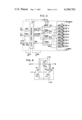
- FIG. 3 illustrates specific formation of the analog switch circuits IC 1 and IC 2 .
- AND 1 and AND 2 are AND circuits
- INV 1 to INV 11 are inverters
- NAND 1 to NAND 4 are NAND circuits
- LLC is a logic level converter circuit
- S 1 to S 8 are switch circuits each of which is formed, for example, of MOS transistors M 1 to M 7 .
- the switch circuit of FIG. 4 is a standard switching circuit which operates in the conventional manner.
- One of four groups of clock pulses OX to 3X different in phases applied to terminals 12, 14, 15 and 11 respectively is selected to be outputted through a COMMON terminal 13, depending on conditions of signals C 1 and C 2 applied to terminals 9 and 10, i.e., (0,0), (0,1), (1,0) or (1,1).
- one of four groups of clock pulses 0Y to 3Y different in phases, applied to terminals 1, 5, 2 and 4 respectively is selected to be outputted through a COMMON terminal depending on the conditions of the signals C 1 and C 2 .
- FIG. 5 illustrates one specific form of one of two synchronous binary counters (four digits) constituting the counter IC 3 .
- INV 12 to INV 23 are inverters
- NOR 1 is a NOR circuit
- NAND 5 and NAND 6 are NAND circuits
- FF 1 to FF 4 are flip-flop circuits.
- One of the binary counters counts occurrences of mis-reading of the data, and the other is responsive thereto to output a clock selecting signal through the output terminals O 1 and O 2 of the counter IC 3 .
- a horizontal synchronizing signal is utilized as a synchronizing signal for the data, too.
- circuits for separating the horizontal synchronizing signal are usually mass-produced ones and have significant variances therebetween, so that it is quite difficult for all the circuits to generate data clock pulses at desired timing.
- the circuit of the present invention can also be employed with advantages to achieve desired timing.
Abstract
A circuit for correcting data reading clock pulses, comprising a data reading device for reading data in response to clock pulses of a group or groups of different phases selected by one or more switches, a detector adapted to detect mis-reading of the data, a switch means and a switch control means. The switch control means is actuated by a detection signal of mis-reading to control the switch means so as to select clock pulse group or groups desired for accurate reading of the data.
Description
1. Field of the Invention
This invention relates to a circuit for correcting data reading clock pulses, and more particularly to an improved circuit for correcting data reading clock pulses which is capable of eliminating mis-reading of data due to timing error of the data reading clock pulses.
2. Description of the Prior Art
In general, reading clock pulses are required to read n-bits of data within a period of time T and the timing of the pulses must be synchronized with an external signal. To this end, a synchronizing signal is generally required. Where no special synchronizing signal is provided for the data reading clock pulses, a start bit is formed, as dummy data, in the data to be read, so as to act as the desired synchronizing signal.
In the former case where a synchronizing signal per se is used, however, it is quite difficult to have the reading clock pulses coincide with the synchronizing signal when mass-produced digital circuits etc. are employed. This has been a problem to be solved. On the other hand, the latter case where a start bit is used has the disadvantage that an additional bit needs to be inserted in a limited time space and a time space for one data bit is reduced.
It is therefore an object of the present invention to provide a circuit for correcting data reading clock pulses which is capable of obviating the aforesaid disadvantages.
It is a more specific object of the present invention to provide a circuit for correcting data reading clock pulses which is capable of eliminating mis-reading of data without using a special synchronizing signal, a start bit, etc. and by automatically selecting optimum clock pulses from roughly synchronized n-phase clock pulse groups.
A circuit for correlating data reading clock pulses, including a clock pulse generator for generating a plurality of groups of clock pulses different in phases, a switch for selecting and outputting one or more groups of clock pulses from the plurality of groups of clock pulses, a device for reading data in response to one or more groups of clock pulses selected by the switch, a detector for detecting mis-reading of the data and outputting a detection signal, and a switch control responsive to the detection signal to control the switch so as to continue selection of another group or groups of clock pulses until correct data reading is accomplished.
FIG. 1 is a block diagram of one form of a circuit for correcting data reading clock pulses in accordance with the present invention;
FIG. 2 is a block diagram of one specific form of a principal portion of the circuit illustrated in FIG. 1;
FIG. 3 shows IC1 and IC2 of FIG. 2;
FIG. 4 shows one of the switch circuits S1 -S8 of FIG. 3; and
FIG. 5 shows IC3 of FIG. 2.
Referring now to the accompanying drawings, there is illustrated one preferred mode of the invention. In FIG. 1, numeral 1 designates a data reading device such as a known tape reader. Numeral 2 is a detector for detecting misreading of data, 3 is a switch control circuit, SW1 to SWn are switches and 4 is a clock pulse generator for generating clock pulses of groups φ1 to φn of n different phases each generally synchronized with a desired external signal. A time of one data bit is divided into n parts to form the clock pulse groups φ1 to φn of n phases. Out of these clock pulse groups φ1 to φn, a given number of clock pulse groups or groups are selected by corresponding switches SW1 to SWn closed by the switch control circuit 3. In the illustrated embodiment, one clock pulse group is selected and the selected clock pulse φout is outputted to the data reading device 1.
If there is an error in data reading by the device 1 effected in response to the clock pulse φout, the detector detects the error and the switch control circuit 3 is actuated by the detection signal so that the switch in a closed position is opened and another switch is closed to select another clock pulse group. Thus, the switch control circuit 3 automatically goes on scanning of the switches, closing the switches sequentially, in response to the detection signals of mis-reading of the data, until a clock pulse φout desired for accurate data reading is obtained. The detector 2 may be a known detector which is adapted to detect an error through an output of a parity check or continuous-transmission check of the read-out data.
FIG. 2 illustrates one example of an arrangement of the switches SW and the switch control circuit 3 employing IC circuits. In the FIG., IC1 and IC2 are analog switch circuits and have functions equivalent to those of the switches SW1 to SWn. In the illustrated arrangement, the circuit IC1 receives input clock pulses φ2 to φ7 and selectively outputs one of the clock pulses φ2 to φ5 to an output Φ8 and outputs one of the clock pulses φ3 to φ6 to an output Φ1. The circuit IC2 receives inputs φ4 to φ7 and outputs one of the clock pulses φ4 to φ7 to an output Φ2.
IC3 is a counter having a function of the switch control circuit 3 as mentioned above. An input terminal I2 of the counter IC3 receives a detection output (for example "0" for mis-reading and "1" for correct reading) from the detector 2, while an input terminal I1 receives a clock pulse φ8. I3 is a reset terminal. O1 and O2 are output terminals and connected to control terminals C1 and C2 of the analog switch circuit, respectively. Numerals indicated around the respective IC circuit IC1 to IC3 designate terminal numbers of IC chips of the respective circuits.
When mis-reading occurs, the detection output "0" is applied to the input terminal I2 of the counter IC3 and the counter IC3 starts to count the clock pulses φ8 in response to the detection output. If the mis-reading remains uncorrected, for example, after eight clock pulses have been counted, i.e., the data reading device has failed to correctly read the data eight times, level conditions of the output terminals 01 and 02 are changed and, in response thereto, each of the analog switch circuits changes respective input clock pulse to a different one, namely, an input clock pulse which lags or leads by one phase. Thus, scanning of input clock pulses is repeated until the mis-reading of the data is eliminated.
FIG. 3 illustrates specific formation of the analog switch circuits IC1 and IC2 . In the figure, AND1 and AND2 are AND circuits, INV1 to INV11 are inverters, NAND1 to NAND4 are NAND circuits, LLC is a logic level converter circuit, and S1 to S8 are switch circuits each of which is formed, for example, of MOS transistors M1 to M7. The switch circuit of FIG. 4 is a standard switching circuit which operates in the conventional manner. One of four groups of clock pulses OX to 3X different in phases applied to terminals 12, 14, 15 and 11 respectively is selected to be outputted through a COMMON terminal 13, depending on conditions of signals C1 and C2 applied to terminals 9 and 10, i.e., (0,0), (0,1), (1,0) or (1,1). Similarly, one of four groups of clock pulses 0Y to 3Y different in phases, applied to terminals 1, 5, 2 and 4 respectively is selected to be outputted through a COMMON terminal depending on the conditions of the signals C1 and C2.
FIG. 5 illustrates one specific form of one of two synchronous binary counters (four digits) constituting the counter IC3. In the figure, INV12 to INV23 are inverters, NOR1 is a NOR circuit, NAND5 and NAND6 are NAND circuits and FF1 to FF4 are flip-flop circuits. One of the binary counters counts occurrences of mis-reading of the data, and the other is responsive thereto to output a clock selecting signal through the output terminals O1 and O2 of the counter IC3.
Where various data is superposed on a video signal as in a toll TV broadcast, in general, a horizontal synchronizing signal is utilized as a synchronizing signal for the data, too. However, circuits for separating the horizontal synchronizing signal are usually mass-produced ones and have significant variances therebetween, so that it is quite difficult for all the circuits to generate data clock pulses at desired timing. In such a case, the circuit of the present invention can also be employed with advantages to achieve desired timing.
Further in accordance with the present invention, there is no need to provide a start bit or stop bit within a limited time space so that a time per one bit data can be utilized effectively.
Claims (4)
1. A circuit for correcting data reading clock pulses, which comprises:
a means for generating a plurality of groups of clock pulses of different phases;
a switch means for selecting and outputting one or more groups of clock pulses from said plurality of groups of clock pulses;
a means for reading data in response to said one or more groups of clock pulses selected by said switch means;
a means for detecting mis-reading of the data and outputting a detection signal indicating mis-reading; and
a switch control means responsive to said detection signal to control said switch means so as to repeatedly select another group or groups of clock pulses until correct data reading is accomplished as determined by absence of said detection signal.
2. A circuit for correcting data reading clock pulses as claimed in claim 1, wherein said switch means includes a plurality of switches which are adapted to receive, at their respective inputs, corresponding groups of clock pulses, respectively, and adapted to be controlled by said switch control means so as to be closed or opened in response to the detection signal of mis-reading of the data.
3. A circuit for correcting data reading clock pulses as claimed in claim 1, wherein said switch control means is formed of a counter, said counter being adapted to count one group of clock pulses allocated thereto out of said plurality of groups of clock pulses and cause said switch means to select another group or groups of clock pulses of different phases when the mis-reading of the data remains uncorrected after said counter has counted a predetermined number of said clock pulses allocated thereto.
4. A method for correcting data reading clock pulses which comprises:
generating a plurality of groups of clock pulses of different phases;
selecting one or more groups of clock pulses from said plurality of groups of clock pulses;
reading data in response to the selected one or more groups of clock pulses;
detecting mis-reading of the data; and
repeatedly selecting another group or groups of clock pulses, upon detection of mis-reading, until correct data reading is accomplished.
Applications Claiming Priority (2)
| Application Number | Priority Date | Filing Date | Title |
|---|---|---|---|
| JP54-117375 | 1979-09-14 | ||
| JP11737579A JPS5642825A (en) | 1979-09-14 | 1979-09-14 | Compensating circuit for data reading clock |
Publications (1)
| Publication Number | Publication Date |
|---|---|
| US4348762A true US4348762A (en) | 1982-09-07 |
Family
ID=14710085
Family Applications (1)
| Application Number | Title | Priority Date | Filing Date |
|---|---|---|---|
| US06/176,974 Expired - Lifetime US4348762A (en) | 1979-09-14 | 1980-08-11 | Circuit for correcting data reading clock pulses |
Country Status (2)
| Country | Link |
|---|---|
| US (1) | US4348762A (en) |
| JP (1) | JPS5642825A (en) |
Cited By (11)
| Publication number | Priority date | Publication date | Assignee | Title |
|---|---|---|---|---|
| EP0131662A1 (en) * | 1980-04-30 | 1985-01-23 | The Manitoba Telephone System | Distributed network synchronization system |
| EP0170225A2 (en) * | 1984-07-28 | 1986-02-05 | Fujitsu Limited | Radio receiver |
| US4616335A (en) * | 1983-06-30 | 1986-10-07 | International Business Machines Corporation | Apparatus for suspending a system clock when an initial error occurs |
| US4644568A (en) * | 1985-03-28 | 1987-02-17 | At&T Bell Laboratories | Timing signal distribution arrangement |
| US4955040A (en) * | 1987-10-27 | 1990-09-04 | Siemens Aktiengesellschaft | Method and apparatus for generating a correction signal in a digital clock recovery device |
| US4972443A (en) * | 1987-11-24 | 1990-11-20 | Siemens Aktiengesellschaft | Method and arrangement for generating a correction signal for a digital clock recovery means |
| US5117442A (en) * | 1988-12-14 | 1992-05-26 | National Semiconductor Corporation | Methods and circuits for synchronizing signals in a modular redundant fault tolerant computer system |
| US5621774A (en) * | 1993-11-30 | 1997-04-15 | Hitachi, Ltd. | Method and apparatus for synchronizing parallel data transfer |
| US20010032323A1 (en) * | 2000-04-06 | 2001-10-18 | Konica Corporation | Clock generating device |
| US20030095611A1 (en) * | 2001-11-16 | 2003-05-22 | Budde Wolfgang Otto | Receiving circuit for receiving message signals |
| EP1793523A1 (en) * | 2005-12-02 | 2007-06-06 | Yokogawa Electric Corporation | Receiver deploying error detecting means for synchronisation |
Families Citing this family (2)
| Publication number | Priority date | Publication date | Assignee | Title |
|---|---|---|---|---|
| JPH0744527B2 (en) * | 1986-01-31 | 1995-05-15 | 株式会社日立製作所 | Bit synchronization circuit |
| JP2547005B2 (en) * | 1987-02-18 | 1996-10-23 | 松下通信工業株式会社 | Error correction method |
Citations (8)
| Publication number | Priority date | Publication date | Assignee | Title |
|---|---|---|---|---|
| US3530663A (en) * | 1967-09-01 | 1970-09-29 | Patek Philippe Sa | Automatic and continuous time adjusting device for a clock |
| US3573727A (en) * | 1968-11-04 | 1971-04-06 | Bell Telephone Labor Inc | Feedback arrangement for minimizing a system parameter |
| US3646517A (en) * | 1969-06-30 | 1972-02-29 | Int Standard Electric Corp | Error detection and correction system |
| US3840855A (en) * | 1972-07-10 | 1974-10-08 | Cit Alcatel | Automatic selector for line corrector for data transmission |
| US3938086A (en) * | 1974-04-11 | 1976-02-10 | Societa Italiana Telecomunicazioni Siemens S.P.A. | Circuit arrangement for correcting slip errors in pcm receivers |
| US4203003A (en) * | 1978-12-04 | 1980-05-13 | Gte Automatic Electric Laboratories Incorporated | Frame search control for digital transmission system |
| US4218771A (en) * | 1978-12-04 | 1980-08-19 | Rockwell International Corporation | Automatic clock positioning circuit for a digital data transmission system |
| US4232387A (en) * | 1977-12-21 | 1980-11-04 | Societa Italiana Telecomunicazioni Siemens S.P.A. | Data-transmission system using binary split-phase code |
Family Cites Families (2)
| Publication number | Priority date | Publication date | Assignee | Title |
|---|---|---|---|---|
| JPS4911008A (en) * | 1972-05-26 | 1974-01-31 | ||
| JPS5426165B2 (en) * | 1974-01-09 | 1979-09-03 |
-
1979
- 1979-09-14 JP JP11737579A patent/JPS5642825A/en active Pending
-
1980
- 1980-08-11 US US06/176,974 patent/US4348762A/en not_active Expired - Lifetime
Patent Citations (8)
| Publication number | Priority date | Publication date | Assignee | Title |
|---|---|---|---|---|
| US3530663A (en) * | 1967-09-01 | 1970-09-29 | Patek Philippe Sa | Automatic and continuous time adjusting device for a clock |
| US3573727A (en) * | 1968-11-04 | 1971-04-06 | Bell Telephone Labor Inc | Feedback arrangement for minimizing a system parameter |
| US3646517A (en) * | 1969-06-30 | 1972-02-29 | Int Standard Electric Corp | Error detection and correction system |
| US3840855A (en) * | 1972-07-10 | 1974-10-08 | Cit Alcatel | Automatic selector for line corrector for data transmission |
| US3938086A (en) * | 1974-04-11 | 1976-02-10 | Societa Italiana Telecomunicazioni Siemens S.P.A. | Circuit arrangement for correcting slip errors in pcm receivers |
| US4232387A (en) * | 1977-12-21 | 1980-11-04 | Societa Italiana Telecomunicazioni Siemens S.P.A. | Data-transmission system using binary split-phase code |
| US4203003A (en) * | 1978-12-04 | 1980-05-13 | Gte Automatic Electric Laboratories Incorporated | Frame search control for digital transmission system |
| US4218771A (en) * | 1978-12-04 | 1980-08-19 | Rockwell International Corporation | Automatic clock positioning circuit for a digital data transmission system |
Cited By (14)
| Publication number | Priority date | Publication date | Assignee | Title |
|---|---|---|---|---|
| EP0131662A1 (en) * | 1980-04-30 | 1985-01-23 | The Manitoba Telephone System | Distributed network synchronization system |
| US4616335A (en) * | 1983-06-30 | 1986-10-07 | International Business Machines Corporation | Apparatus for suspending a system clock when an initial error occurs |
| EP0170225A2 (en) * | 1984-07-28 | 1986-02-05 | Fujitsu Limited | Radio receiver |
| EP0170225A3 (en) * | 1984-07-28 | 1987-10-21 | Fujitsu Limited | Radio receiver |
| US4644568A (en) * | 1985-03-28 | 1987-02-17 | At&T Bell Laboratories | Timing signal distribution arrangement |
| US4955040A (en) * | 1987-10-27 | 1990-09-04 | Siemens Aktiengesellschaft | Method and apparatus for generating a correction signal in a digital clock recovery device |
| US4972443A (en) * | 1987-11-24 | 1990-11-20 | Siemens Aktiengesellschaft | Method and arrangement for generating a correction signal for a digital clock recovery means |
| US5117442A (en) * | 1988-12-14 | 1992-05-26 | National Semiconductor Corporation | Methods and circuits for synchronizing signals in a modular redundant fault tolerant computer system |
| US5621774A (en) * | 1993-11-30 | 1997-04-15 | Hitachi, Ltd. | Method and apparatus for synchronizing parallel data transfer |
| US20010032323A1 (en) * | 2000-04-06 | 2001-10-18 | Konica Corporation | Clock generating device |
| US20030095611A1 (en) * | 2001-11-16 | 2003-05-22 | Budde Wolfgang Otto | Receiving circuit for receiving message signals |
| US7278071B2 (en) * | 2001-11-16 | 2007-10-02 | Nxp B.V. | Receiving circuit for receiving message signals |
| EP1793523A1 (en) * | 2005-12-02 | 2007-06-06 | Yokogawa Electric Corporation | Receiver deploying error detecting means for synchronisation |
| US20070140227A1 (en) * | 2005-12-02 | 2007-06-21 | Yokogawa Electric Corporation | Receiver |
Also Published As
| Publication number | Publication date |
|---|---|
| JPS5642825A (en) | 1981-04-21 |
Similar Documents
| Publication | Publication Date | Title |
|---|---|---|
| US4348762A (en) | Circuit for correcting data reading clock pulses | |
| US4625321A (en) | Dual edge clock address mark detector | |
| EP0455957A2 (en) | Odd/even field detector for video signals | |
| US4641326A (en) | Counter circuit operable in synchronism with frame or digital data signal | |
| US4354176A (en) | A-D Converter with fine resolution | |
| US3737895A (en) | Bi-phase data recorder | |
| US3971920A (en) | Digital time-off-event encoding system | |
| US5969553A (en) | Digital delay circuit and digital PLL circuit with first and second delay units | |
| DE3367061D1 (en) | Receiver with electronically tunable tuning circuit | |
| US5221906A (en) | Program control digital pulse generator | |
| US4010423A (en) | Multi-function remote control ic | |
| JP2584324B2 (en) | VTR playback mode identification circuit | |
| US6367027B1 (en) | Skew pointer generation | |
| US4771402A (en) | Address comparator | |
| US5231509A (en) | Burst gate pulse generating device for use in image signal reproducing system | |
| US6928530B2 (en) | Method and device for sequential readout of a memory with address jump | |
| US5459752A (en) | Simple digital method for controlling digital signals to achieve synchronization | |
| JPS6323437A (en) | Synchronous detecting circuit | |
| SU1575187A1 (en) | Device for monitoring code sequences | |
| SU468243A1 (en) | Interface device | |
| SU643973A1 (en) | Device for control of storage element-based accumulator with non-destructive reading-out of information | |
| JP2506407B2 (en) | Clock synchronous data transmission system | |
| SU1265755A1 (en) | Information input-output device | |
| SU1667121A1 (en) | Data input device | |
| KR930005775Y1 (en) | Optical disk operating device |
Legal Events
| Date | Code | Title | Description |
|---|---|---|---|
| STCF | Information on status: patent grant |
Free format text: PATENTED CASE |