US4225807A - Readout scheme of a matrix type thin-film EL display panel - Google Patents
Readout scheme of a matrix type thin-film EL display panel Download PDFInfo
- Publication number
- US4225807A US4225807A US05/923,646 US92364678A US4225807A US 4225807 A US4225807 A US 4225807A US 92364678 A US92364678 A US 92364678A US 4225807 A US4225807 A US 4225807A
- Authority
- US
- United States
- Prior art keywords
- display panel
- transistors
- current
- film
- readout
- Prior art date
- Legal status (The legal status is an assumption and is not a legal conclusion. Google has not performed a legal analysis and makes no representation as to the accuracy of the status listed.)
- Expired - Lifetime
Links
Images


Classifications
-
- G—PHYSICS
- G11—INFORMATION STORAGE
- G11C—STATIC STORES
- G11C11/00—Digital stores characterised by the use of particular electric or magnetic storage elements; Storage elements therefor
- G11C11/02—Digital stores characterised by the use of particular electric or magnetic storage elements; Storage elements therefor using magnetic elements
- G11C11/14—Digital stores characterised by the use of particular electric or magnetic storage elements; Storage elements therefor using magnetic elements using thin-film elements
-
- G—PHYSICS
- G09—EDUCATION; CRYPTOGRAPHY; DISPLAY; ADVERTISING; SEALS
- G09G—ARRANGEMENTS OR CIRCUITS FOR CONTROL OF INDICATING DEVICES USING STATIC MEANS TO PRESENT VARIABLE INFORMATION
- G09G3/00—Control arrangements or circuits, of interest only in connection with visual indicators other than cathode-ray tubes
- G09G3/20—Control arrangements or circuits, of interest only in connection with visual indicators other than cathode-ray tubes for presentation of an assembly of a number of characters, e.g. a page, by composing the assembly by combination of individual elements arranged in a matrix no fixed position being assigned to or needed to be assigned to the individual characters or partial characters
- G09G3/22—Control arrangements or circuits, of interest only in connection with visual indicators other than cathode-ray tubes for presentation of an assembly of a number of characters, e.g. a page, by composing the assembly by combination of individual elements arranged in a matrix no fixed position being assigned to or needed to be assigned to the individual characters or partial characters using controlled light sources
- G09G3/30—Control arrangements or circuits, of interest only in connection with visual indicators other than cathode-ray tubes for presentation of an assembly of a number of characters, e.g. a page, by composing the assembly by combination of individual elements arranged in a matrix no fixed position being assigned to or needed to be assigned to the individual characters or partial characters using controlled light sources using electroluminescent panels
-
- G—PHYSICS
- G09—EDUCATION; CRYPTOGRAPHY; DISPLAY; ADVERTISING; SEALS
- G09G—ARRANGEMENTS OR CIRCUITS FOR CONTROL OF INDICATING DEVICES USING STATIC MEANS TO PRESENT VARIABLE INFORMATION
- G09G2310/00—Command of the display device
- G09G2310/02—Addressing, scanning or driving the display screen or processing steps related thereto
- G09G2310/0264—Details of driving circuits
- G09G2310/0267—Details of drivers for scan electrodes, other than drivers for liquid crystal, plasma or OLED displays
-
- G—PHYSICS
- G09—EDUCATION; CRYPTOGRAPHY; DISPLAY; ADVERTISING; SEALS
- G09G—ARRANGEMENTS OR CIRCUITS FOR CONTROL OF INDICATING DEVICES USING STATIC MEANS TO PRESENT VARIABLE INFORMATION
- G09G2310/00—Command of the display device
- G09G2310/02—Addressing, scanning or driving the display screen or processing steps related thereto
- G09G2310/0264—Details of driving circuits
- G09G2310/0275—Details of drivers for data electrodes, other than drivers for liquid crystal, plasma or OLED displays, not related to handling digital grey scale data or to communication of data to the pixels by means of a current
Landscapes
- Engineering & Computer Science (AREA)
- Computer Hardware Design (AREA)
- Physics & Mathematics (AREA)
- General Physics & Mathematics (AREA)
- Theoretical Computer Science (AREA)
- Control Of Indicators Other Than Cathode Ray Tubes (AREA)
- Control Of El Displays (AREA)
Abstract
Between adjacent matrix type electrodes in a thin-film EL display panel, one of which is transparent, there is disposed an EL layer sandwiched by a pair of dielectric layers, which manifests a hysteresis curve when plotted with respect to the applied voltage vs light intensity characteristics. The thin-film EL display panel is further provided with at least one reference electrode. In reading out the memory state of the display panel, current is derived which has an amplitude equal to the difference between the current drawn through the reference electrode and the readout current.
Description
The present invention relates to a memory readout scheme for a three-layered thin-film EL display panel structure which manifests hysteresis memory effects when pletted with respect to applied voltage and light emission intensity, and more particularly to a readout scheme of a thin-film EL display panel having a matrix electrode pattern with an improved signal to noise (SN) ratio.
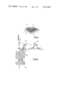
As disclosed and illustrated in U.S. Pat. No. 3,975,661 DRIVING METHOD FOR A THIN-FILM ELECTROLUMINESCENT ELEMENT OF A THREE-LAYER CONSTRUCTION assigned to the same assignee as this application, a thin-film EL display has a three-layered structure shown in a perspective view partly in cross section of FIG. 1, the disclosure of which is incorporated herein. A predetermined number of transparent electrode strips 2 are disposed on a glass support 1. Further, a layer 3 of dielectric material such as Y2 O3, Si3 N4, TiO2 and Al2 O3, a layer 4 of electroluminescent material, for example, ZnS doped with Mn (yellowish orange light) and a second layer 31 of dielectric material such as Y2 O3, Si3 N4, TiO2, Al2 O3 are disposed by a well known thin-film technique such as vacuum deposition and sputtering each having a thickness ranging from 500 to 10,000 A. This results in a double-isolation three-layered structure of the EL display panel. A different family of strip electrodes 5 is disposed in a direction normal to the direction of the transparent electrodes 2 to form an electrode matrix array together with the transparent electrodes. With such a three-layered thin-film EL display panel, if one of the first family 2 of the electrodes and one of the second family 5 of the electrodes are selected, a minute area, where the selected ones of the first and second family of electrodes cross each other, will emit light. This corresponds to a picture element of an image like a character, a symbol and a pattern being displayed.
The EL panel with a structure is more attractive than the prior art dispersed powder type EL panel from the standpoint of light intensity, working life and performance stability. The above described EL panel is more advantageous than the prior art in that it exhibits a hysteresis curve when plotted with respect to applied voltage and light emission intensity, as seen from FIG. 2(b). When first applying a pulse of the voltage amplitude V1 as shown in FIG. 2(a), the intensity of the EL panel is at the value B1 as shown in FIGS. 2(b) and 2(c). The sustained voltage V1 is correlated as V1 >Vth wherein Vth is the threshold voltage level for light emission. Consecutive application of the sustained voltage V1 permits the intensity B1 to be held. If a write voltage V2 is then applied, the brightness will than go up to B3. Even if the sustained voltage V1 is reached again in a brief period, the intensity will settle at a value B2 higher than the previous one B1. Consecutive application of the sustained voltage V1 keeps the brightness B2 constant. When an erase voltage V3 is applied, this causes the intensity to drop. If the sustain voltage is reapplied, then the intensity will settle at B1. This time relationship is illustrated by using the same time references t1, t2 . . . t21 as in FIGS. 2(a) to 2(c). The hysteresis phenomenon may trace a different loop according to a selection of the amplitude, pulse width and frequency of the write voltage. In other words, a half tone display is also possible. Once the write voltage or the erase voltage has been applied in this way, the individual picture elements keep emitting light without losing their own tones, in response to the application of the sustain pulse. Though the respective levels of voltage depend mainly on compositions, thicknesses, manufacturing conditions and waveforms of applied voltages, the inventors' experiments revealed that Vth =200 V, V1 =210 V, V2 =210 to 280 V and V3 =190 V, for example.
As noted earlier, the three-layered thin-film EL display panel is capable of reading out, electrically, the memory state thereof in addition to the functions of writing, erasing and sustaining by a proper selection of applied voltage, pulse width and pulse frequency.
The thin-film EL panel can be considered a capacitive element because of the fact that the electroluminescent layer sandwiched by the pair of dielectric layers, so that displacement current may flow through the EL panel when applying the sustain voltage. If the display element is latched in the light emitting state or write state, the displacement current will flow in response to the application of the sustain voltage plus current which is proportional to the brightness. This combined current is called polarization current. Actually because the background is held at some potential even in the erase state, a small amount of the displacement current will flow correspondingly. For example, while the EL element is supplied with the sustained voltage pulse as seen from FIG. 3(a), current flowing through the EL element will assume the waveform shown by the solid line I in FIG. 3(b) in the erase state and the waveform which is combined with the polarization current as depicted by the dotted line II in the write state.
The inventors' approach to determine the presence or absence of the polarization current involves a decision as to whether the displacement current exceeds a given amount taking a noise margin into account, thereby determining whether the EL element is in the write state or in the erase state. However, since this method is used to separate the displacement current from the polarization current at a predetermined level, a selection of the predetermined level needs careful consideration. The component of the polarization current over the predetermined level is equal to that minus the noise margin and the absolute value of this signal is extremely small. A signal-to-noise ratio is therefore not good.
It seems possible to remove undesirable current in the erase state by provision of an equivalent circuit consisting of analog elements such as capacitors and resistors which forms current similar to the displacement current or provision of a read only memory which stores the very waveform of that undersirable current in the erase state. Although these approaches are basically applicable to an EL unit element, the following problems will occur with respect to an EL matrix type element.
(1) In the case of matrix driving, the amplitude of the displacement current will vary greatly according to the number of the picture elements to be written and that to be erased. To this end it is rather difficult to form the equivalent circuit or the erase waveform.
(2) In order to efficiently cause light emission from the thin-film EL element, at least electrodes at the display side should be transparent. The transparent electrodes should be disposed at a much narrower interval in order to withstand a higher resistance as in the case where the display density is increased in a matrix display. This leads to a substantial difference in resistance between the display electrode closest to the lead region and that farthest from the same and therefore a substantial variation in the effective applied voltage results. Therefore, even though the same pulse is externally applied, the waveform of current will vary from point to point in the read out mode. This requires a predetermined number of equivalent circuits for storing the respective erase state current waveforms and thus renders a readout scheme complicated and large sized and expensive.
It is therefore an object of the present invention to provide an improved readout scheme for use in a matrix type EL display panel which overcomes the above described problems recognized by the inventors.
A matrix type thin-film EL display device embodying the present invention is provided at a portion of the display electrodes thereof in addition to a reference electrode. Current flowing through the reference electrode is utilized such that the erase state current or dark current cancels the displacement current. This makes it possible to pick up only the polarization current which is indicative of the internal state of the EL display device.
Other objects and many of the attendant advantages of the present invention will be easily appreciated as the same becomes better understood by reference to the following detailed description which should be considered in conjunction with the accompanying drawings in which like reference numerals designate like parts throughout the figures thereof, and wherein:
FIG. 1 is a perspective view partly in cross section of a threelayered structure thin-film EL display panel;
FIG. 2 is a graph showing the relationship between applied voltage and light emission intensity illustrating the operation of the display panel of FIG. 1;
FIG. 3 is a waveform diagram of the current in the readout mode of the display panel;
FIG. 4 is a circuit diagram of one preferred form of the present invention;
FIG. 5 is a circuit diagram of another preferred form of the present invention;
FIG. 6 is a time chart for illustration of operation of the circuit of FIG. 5;
FIG. 7 is a flow chart for illustration of operation of the circuit of FIG. 5;
FIG. 8 is a circuit diagram of still another modification of the present invention; and
FIG. 9 is a time chart associated with the circuit of FIG. 8.
Referring now to FIG. 4, there is illustrated one preferred form of the present invention which can be generally divided into six blocks.
The first block is a sustain driver circuit 10. Through FIG. 4 shows a three-phase sustain driver circuit, one which is clocked with four-phase timing signals can be used. Two sustain voltage sources E1 and -E2 are prepared and an EL display panel 50 is supplied with three voltages, namely, E1, 0 and -E2, respectively and applied concurrently with the sequential operation of three switches SW1, SW2 and SW3. A transformer T is connected in series with the capacitive component of the EL display device 50 to form a resonant circuit and to enable a highly efficient voltage supply.
The second block is a write and read switch circuit 20 which supplies a write voltage Vw from a voltage source Ew via a switch Wsk (k=1 to m) to a line X sought to be written in when in the write mode. If the line X is desired to be read out with respect to the internal state, the line X is supplied with a readout voltage Vr from a readout driver circuit 70 which is adapted to supply a voltage equal to the sustain voltage Vs.
The third block is a set of switches 30 disposed at the transparent electrodes of the EL display device. All of the switches 30 are shunted during the sustain mode or phase and selected ones of the Y lines are turned on with the remaining Y lines kept off during the write, erase and readout modes.
The fourth block is a write and read separation and sustain voltage amplitude holding circuit 40, and to more particularly a diode circuit adapted to separate write lines from non-write lines and hold the amplitude of resonance driving.
The fifth block 50 is the three-layered structure EL display device of the matrix type as illustrated in FIG. 1 wherein the extreme left electrode from the transparent strip electrodes, is used as the reference electrode r for the purpose of the present invention. Only the electrodes are shown in FIG. 4.
The sixth block is a readout circuit which plays an important role in the present invention. An in-phase signal cancelling amplifier 61 cancels the voltage developed across a resistor R1, which is connected in common to the respective electrodes 1 to n, and a counterpart is developed across a resistor R2, connected to the reference electrode r, with respect to each other and therefore picks up only the polarization current.
Specification of an 8 inch EL panel devised by the inventors is as follows:
______________________________________
line pitch:    two lines / mm
               X lines (transparent electrodes) 320
               Y lines (Al electrodes) 240
display character:
               5 by 7 dot pattern
               64 sorts of Roman letters, Arabic
               letters and symbols
the number of display
               X direction 52 characters
characters:    Y direction 24 lines
               maximum number 1248 characters
the number of effective
               X direction 260 lines
display lines: (character interval 1 line)
               Y direction 168 lines
               (line interval 2 lines)
______________________________________
Returning to FIG. 4, the first sustain switch SW1 is closed at a first timing φ1 so that a difference between a third hold potential VH and the first source voltage E1 is applied across the capacitive element (in the given example the entire EL display panel is considered approximately as a capacitor element Ct of a predetermined capacitance). A first hold potential can be represented below.
V.sub.sl =E.sub.1 +η(B.sub.1 -V.sub.H) (1)
If the second sustain switch SW2 is closed at a second timing φ2, then a second hold potential will assume:
-V.sub.s2 =-E.sub.2 -η(V.sub.1 +E.sub.2) (2)
Subsequently, if the third sustain switch SW3 is closed at the third timing φ3, then a third hold potential will assume:
V.sub.H =V.sub.2 (3)
The three-phase sustain drive is carried out in this manner. This three-phase sustain drive can reduce the breakdown voltage requirement for switches Dsl -Dsn by performing the write mode with the intermediate potential (in the given example the third hold potential VH).
During application of the intermediate potential (VH), and X and Y lines of a picture point M(i, j) to be written are selected by the write/read switch circuit 20 and the switch 30 for the purpose of supplying the write voltage Vw and carrying on the write mode. The erase mode is carried out similarly with the exception that a picture point is supplied with an erase voltage Ve (not shown).
The readout mode of the present invention is carried out in the following manner. By closure of an X switch DSj and a Y switch WSi associated with a picture element M(i, j) to be read out, that picture element is supplied with the sustain pulse voltage Vs. At this time, pulse current will flow through the resistor R1 and reaching the +terminal of the amplifier 61. Reference current, flowing through a reference point P(j, r) of the reference electrode r, will be developed across the resistor R2. Since the reference line r is not written, the erase state current and, thus, only the displacement current, is derived therefrom. This is supplied to the-terminal of the amplifier 61. Accordingly, with the amplifier 61, only the displacement current, though the picture point being read out, is cancelled by current developed across the resistor R2. A differential voltage is derived so that only the polarization current is picked up when the picture element being read out is in the write state. The current will be insignificant (namely, zero) as long as all the picture elements being read out are in the erase state.
As described above, since the present invention employs, (as the reference electrode only one transparent electrode) within the EL display device, the output from that reference electrode results in a displacement current which is equal to the displacement current flowing in fact through the picture elements being read out despite influences of the electrode resistance and the number of the picture elements present in the write state. In addition, the horizontal scanning electrodes, and not the picture elements M being read out, are grounded and fixed at zero potential to thereby facilitate the performance of the readout mode without the need to use troubling crosstalk capacitors. Thus, the present invention makes it possible to obtain signals with a signal to noise ratio of an approximately ideal value.
Though only one reference electrode is provided in the embodiment of FIG. 4, two reference electrodes may be provided instead as in the case where contact areas of the horizontal scanning electrodes are disposed alternatively at the upper portion or at the lower portion so as to increase the electrode density. It is further desirable to avoid wrong operations which may be caused by variations in the amplitude of the displacement current due to variations in the number of the picture elements in the write state along the horizontal scanning electrodes.
FIG. 5 is another embodiment of the present invention provided for taking the above problem into account, which is adapted to read out data, with the blocks 10 and 40 omitted. This circuit is used to compensate for variations in the level of the displacement current through the utilization of a vertical scanning electrode m.
The readout output is applied to a level compensation and readout signal decision circuit 80. An analog comparator 81 receives at the + terminal thereof the output of an amplifier 71 and the - terminal thereof the output of a digital to analog converter 82. The output of the analog comparator 81 is supplied to an AND gate 83 which also receives the readout pulse. The output of the AND gate 83 is applied to an input terminal c of a flip-flop 84 which holds the data which has been read out. The output of the vertical scanning electrode m is sent to a controlling microprocessor 85 which in turn loads data into the digital to analog converter 82 via a data line 86.
A time chart associated with the circuit 80 is depicted in FIG. 6. While the sustain pulse Ps is applied as seen from FIG. 6(a), selected picture element current is obtainable through a selected picture element upon application of the readout pulse Pr. In FIG. 6(b), the waveform E depicted by the solid line is the erase state current and the waveform W depicted by the dotted line is the write state current.
Within the analog comparator 81, the selected picture element current is compared with the analog output S of the digital to analog converter (see FIG. 6(c)). As a result, the logic output "1" or "0" is outputted in accordance with the results of the comparison. The logic output is available from the AND gate 83. The flip flop 84 is inverted in response to the output of the AND gate 83 to sustain the readout output. Since the flip flop is adapted to receive a clear pulse at the terminal Cr thereof immediately before the readout mode, the flip flop is set in accordance with the level of the readout current.
The events in sequence in reading out the state of the point M(i, j) are described with reference to a flow chart of FIG. 7.
First of all, the first step is executed to select the vertical scanning electrode m and the horizontal scanning electrode j and to start evaluating an erase level of the reference picture element (m, j) utilizing the analog to digital conversion. In the succeeding or second step, a data register and a test bit register is loaded with only MSB. The third step is carried out where the contents of the data register are sent to the digital to analog converter 82. In the fourth step, the thin-film EL panel is supplied with the readout pulse and then the contents of the flip flop 84 are checked up. The fifth step is executed to decide whether the output of the flip flop 84 is "1" and, if a NO answer is given, the sixth step is executed to perform an exclusive OR logic operation on the data register and the test bit register so as to clear that bit. In the case of a YES answer the seventh step is carried out to decide whether the test bit is LSB. If a NO answer is concluded during the seventh step, the eighth step is executed to shift the contents of the test bit register one bit to the right. In the presence of a YES answer, the tenth and following steps are reached to detect the contents of the selected picture elements. In the ninth step, the contents of the data register is added to the contents of the test bit register, the results of the addition being loaded again to the data register. Subsequent to this, the third step is restarted.
During the tenth step the vertical scanning electrode i and the horizontal scanning electrode j are selected. The erase level data of the reference picture element obtained during the eleventh step is provided for the digital to analog converter 82 together with an appropriate margin. In the twelfth step, the readout pulse is supplied to investigate the flip flop 84. In the thirteenth step, it is decided whether the output is "1" and, when a YES answer is given, it is concluded, during the fourteenth step, that (i, j) is now in the write state. In the case of a NO answer, the fifteenth step confirms that (i, j) is now in the erase state.
When it is desired to read out the contents of the picture elements in sequence, it will be unnecessary to carry on the time consuming analog to digital conversion in advance by evaluating the erase levels of the picture elements (m, o) to (m, n-1) plus an appropriate margin.
When implementing the switches in the block 30 include transistors, it is desirable that the number of necessary transistors per electrode be as small as possible. While carrying on the write mode and erase mode on one or more selected picture elements, the horizontal scanning electrodes which include the selected picture elements (these are called selected line electrodes hereinafter) should be grounded and the horizontal scanning electrodes which do not include the selected picture elements (these are called non-selected line electrodes hereinafter) should be kept off. During the readout mode, all the non-selected line electrodes, except for the selected line electrodes, should be grounded with the latter kept off.
A circuit having such functions is illustrated in FIG. 8, and includes: a plus side sustain pulse which supplies a high voltage, high power transistor 101 which is supplied with a plus side sustain pulse signal PSUS; electrode separating diodes 102 operable during the application of the plus side sustain pulse; the write mode, erase mode and readout mode; second diodes 103 which turn on all the high voltage transistors (except transistors connected to the selected line electrodes during the readout mode) in response to the readout pulse; READ and a minus side sustain pulse MSUS which isolates them from each other during the selective write mode and the erase mode; transistors 104 which ground the selected line electrodes during the selective write mode and the erase mode; all the non-selected line electrodes during the readout mode and all the line electrodes during the application of the minus side sustain pulse, and an analog switch 105 which is responsive to a binary address to turn on the transistors 104 connected to the selected line electrodes during the selective write mode and erase mode, and to turn off the same connected to the selected line electrodes during the readout mode; and an open-collector TTL buffer 106 which is responsive to a write pulse WRITE, an erase pulse ERASE and the minus side sustain pulse MSUS. The buffer 106 is of the opencollector type where the base current is adjustable through a resistor R.
In the above illustrated embodiment, the transistors 101 and 104 of FIG. 8 are also provided for the vertical scanning electrodes in order to achieve the sustain driving using the single source voltage +Us (two voltage sources +E1 and -E2 are used in FIGS. 4 and 5). When the transistor 101 at the horizontal scanning electrodes is turned on to enable the supply of the sustain voltage +Vs during the sustain driving, that transistor grounds all the vertical scanning electrodes. When the sustain voltage +Vs is supplied from the vertical scanning electrodes, the transistors 104 are turned on to render all the horizontal scanning electrodes grounded. The sustain driving in the given example is called the seesaw method. Operation of this circuit is described by referring to a time chart of FIG. 9. In FIG. 9, PSUS designates a signal to be applied to the plus side sustain pulse supplying transistor 101 and MSUS designates a signal to be applied to the minus side sustain pulse supplying transistors 104. Though FIG. 9 shows the time relationship at the horizontal scanning electrodes, the time relationship between the signals PSUS and MSUS is reversed at the vertical scanning electrodes.
The readout pulse signal READ is applied to the transistors 104 during the readout mode. At this time the analog switch 105 selects the readout electrodes in response to the binary address signal. Since there is no input to the open-collector type buffer 106, it provides no output so that the base of the selective readout transistor 104 is held at the zero potential. That transistor 104, is turned off and the remaining transistors 104 are turned on. The waveform H in FIG. 9 indicates that the transistor 104 connected to the non-selected line electrodes, are in the on state during the readout mode; and the solid line I indicates that the transistors 104, connected to the selected line electrodes, are in the off state. The time relationship between the minus sustain pulse signal MSUS and the readout pulse signal READ is designated by READ+MSUS in FIG. 9. The write pulse signal or erase pulse signal WRITE+ERASE is applied to the open-collector buffer 106. Simultaneously the analog multiplexer 105 selects the electrodes to be written or erased. The output of the open-collector TTL buffer, therefore, assumes "1" so that the base current is supplied from the voltage source +5 V to the selected line electrodes via the resistor R and the multiplexer 105. It is possible to supply current in the opposite directions during the readout mode, the write or the erase mode because of the bidirectional nature of the multiplexer 105. To this end only the transistors 104, connected to the selected horizontal scanning electrodes, are turned on with the remaining transistors off. The dotted line J in FIG. 9 indicates that the transistors 104, connected to the selected line electrodes, are in the on state during the write mode and the erase mode, whereas the solid line K indicates that the transistors 104 connected to the non-selected line electrodes are in the off state during the write mode or the erase mode. WRITE+ERASE+MSUS in FIG. 9 shows the time relationship between the write pulse signal WRITE, the erase pulse signal ERASE, and the minus sustain pulse signal MSUS which is applied to the open-collector type buffer 106.
In the circuit of FIG. 8, the collectors of the transistors 104 are connected to the switches 60 in order to supply the readout current (from the transistors 104, associated with the selected line electrodes) to the switches 60 of FIGS. 4 and 5.
It is obvious to those skilled in the art that a differential transformer is also applicable for detecting the polarization current instead of the differential amplifier as disclosed with respect to the above embodiments. It is further apparent that the reference electrode may be disposed around the middle of the display panel.
The invention being thus described, it will be obvious that the same may be varied in many ways. Such modifications are not to be regarded as a departure from the spirit and scope of the invention, and all such modifications are intended to be included within the scope of the following claims.
Claims (5)
1. A display device having a plurality of picture elements comprising:
a thin-film EL display panel comprising an EL layer sandwiched by a pair of dielectric layers said EL display panel manifesting a hysteresis curve in the applied voltage vs brightness characteristics, and a matrix electrode array sandwiching said pair of dielectric layers for matrix driving said EL display panel;
reference electrode means disposed on said thin-film EL display panel; and
means for deriving current having an amplitude equal to a difference between the current through said reference electrode and a readout current when reading out the memory state of said display panel.
2. The display device as defined in claim 1 wherein said reference electrode means comprises two reference electrodes extending in opposite directions from each other.
3. The display device as defined claim 1 further comprising circuit means for connecting all of said picture elements not desired to be read out to a ground potential.
4. The display device as set forth in claim 1 wherein selected ones of said picture elements of said thin-film EL display panel desired to be read out are selected by transistors, said transistors being controlled by an analog multiplexer.
5. A display device comprising:
a thin-film EL display panel comprising an EL layer sandwiched by a pair of dielectric layers which manifests a hysteresis curve in the applied voltage vs brightness characteristics, and matrix electrode array means sandwiching said pair of dielectric layers for matrix driving sald EL display panel;
a plurality of transistors respectively connected between said matrix electrode array means of said EL display panel and a ground potential;
first circuit means for supplying all of said transistors with a readout signal and for turning on said transistors;
an analog multiplexer means for selecting said transistors; and
second circuit means for turning off said transistors via said analog multiplexer during the readout mode and for turning on said transistors during the write and erase modes.
Applications Claiming Priority (12)
| Application Number | Priority Date | Filing Date | Title |
|---|---|---|---|
| JP52-84353 | 1977-07-13 | ||
| JP8435277A JPS6010636B2 (en) | 1977-07-13 | 1977-07-13 | Readout device for matrix type thin film EL display device |
| JP8435377A JPS6010637B2 (en) | 1977-07-13 | 1977-07-13 | Readout device for matrix type thin film EL display device |
| JP52-84352 | 1977-07-13 | ||
| JP52090660A JPS5916278B2 (en) | 1977-07-27 | 1977-07-27 | Readout device for matrix type thin film EL display device |
| JP52-90660 | 1977-07-27 | ||
| JP52-105179 | 1977-08-31 | ||
| JP52105179A JPS6010638B2 (en) | 1977-08-31 | 1977-08-31 | Readout device for matrix type thin film EL display device |
| JP52-107423 | 1977-09-06 | ||
| JP10742377A JPS5440030A (en) | 1977-09-06 | 1977-09-06 | Reading circuit for matrix-type thin film el display device |
| JP11620577A JPS6016637B2 (en) | 1977-09-26 | 1977-09-26 | Drive circuit for matrix type thin film EL display device |
| JP52-116205 | 1977-09-26 |
Publications (1)
| Publication Number | Publication Date |
|---|---|
| US4225807A true US4225807A (en) | 1980-09-30 |
Family
ID=27551612
Family Applications (1)
| Application Number | Title | Priority Date | Filing Date |
|---|---|---|---|
| US05/923,646 Expired - Lifetime US4225807A (en) | 1977-07-13 | 1978-07-11 | Readout scheme of a matrix type thin-film EL display panel |
Country Status (4)
| Country | Link |
|---|---|
| US (1) | US4225807A (en) |
| DE (1) | DE2830872C3 (en) |
| FR (1) | FR2397696A1 (en) |
| GB (1) | GB2002561B (en) |
Cited By (8)
| Publication number | Priority date | Publication date | Assignee | Title |
|---|---|---|---|---|
| US4954752A (en) * | 1988-12-09 | 1990-09-04 | United Technologies Corporation | Row driver for EL panels and the like with transformer coupling |
| US4975691A (en) * | 1987-06-16 | 1990-12-04 | Interstate Electronics Corporation | Scan inversion symmetric drive |
| US5138308A (en) * | 1988-06-01 | 1992-08-11 | Commissariat A L'energie Atomique | Microtip fluorescent matrix screen addressing process |
| US5583527A (en) * | 1993-11-26 | 1996-12-10 | Fujitsu Limited | Flat display |
| US6496168B1 (en) * | 1999-10-04 | 2002-12-17 | Autonetworks Technologies, Ltd. | Display element drive device |
| US6534925B2 (en) * | 2000-12-28 | 2003-03-18 | Nec Corporation | Organic electroluminescence driving circuit, passive matrix organic electroluminescence display device, and organic electroluminescence driving method |
| EP1496518A1 (en) * | 2002-04-17 | 2005-01-12 | Sony Corporation | Storage device using resistance varying storage element and reference resistance value decision method for the device |
| CN105845087A (en) * | 2014-12-31 | 2016-08-10 | 广州奥翼电子科技有限公司 | Control method for driving electronic paper, controller, device, and electronic paper display device |
Families Citing this family (2)
| Publication number | Priority date | Publication date | Assignee | Title |
|---|---|---|---|---|
| FR2503495A1 (en) * | 1981-04-03 | 1982-10-08 | Commissariat Energie Atomique | Capacitative touch operated keyboard immune to interference - uses reception electrode signal difference to generate noise free output signal and interference level detection to inhibit key pad operation |
| DE3273873D1 (en) * | 1981-04-03 | 1986-11-20 | Commissariat Energie Atomique | Capacitive keyboard with anti-parasite structure |
Citations (1)
| Publication number | Priority date | Publication date | Assignee | Title |
|---|---|---|---|---|
| US3975661A (en) * | 1973-06-19 | 1976-08-17 | Sharp Kabushiki Kaisha | Driving method for a thin-film electroluminescent element of a three-layer construction |
Family Cites Families (4)
| Publication number | Priority date | Publication date | Assignee | Title |
|---|---|---|---|---|
| US3205403A (en) * | 1957-02-04 | 1965-09-07 | Xerox Corp | Electroluminescent display systems |
| US3967112A (en) * | 1973-06-15 | 1976-06-29 | Sharp Kabushiki Kaisha | Photo-image memory panel and activating method thereof |
| GB1497210A (en) * | 1975-05-13 | 1978-01-05 | Ncr Co | Matrix memory |
| DE2630622C2 (en) * | 1975-07-07 | 1982-03-25 | Sharp K.K., Osaka | Arrangement for controlling a capacitive display element |
-
1978
- 1978-07-11 US US05/923,646 patent/US4225807A/en not_active Expired - Lifetime
- 1978-07-13 GB GB7829700A patent/GB2002561B/en not_active Expired
- 1978-07-13 DE DE2830872A patent/DE2830872C3/en not_active Expired
- 1978-07-13 FR FR7821023A patent/FR2397696A1/en active Granted
Patent Citations (1)
| Publication number | Priority date | Publication date | Assignee | Title |
|---|---|---|---|---|
| US3975661A (en) * | 1973-06-19 | 1976-08-17 | Sharp Kabushiki Kaisha | Driving method for a thin-film electroluminescent element of a three-layer construction |
Cited By (11)
| Publication number | Priority date | Publication date | Assignee | Title |
|---|---|---|---|---|
| US4975691A (en) * | 1987-06-16 | 1990-12-04 | Interstate Electronics Corporation | Scan inversion symmetric drive |
| US5138308A (en) * | 1988-06-01 | 1992-08-11 | Commissariat A L'energie Atomique | Microtip fluorescent matrix screen addressing process |
| US4954752A (en) * | 1988-12-09 | 1990-09-04 | United Technologies Corporation | Row driver for EL panels and the like with transformer coupling |
| US5583527A (en) * | 1993-11-26 | 1996-12-10 | Fujitsu Limited | Flat display |
| US5973655A (en) * | 1993-11-26 | 1999-10-26 | Fujitsu Limited | Flat display |
| US6496168B1 (en) * | 1999-10-04 | 2002-12-17 | Autonetworks Technologies, Ltd. | Display element drive device |
| US6534925B2 (en) * | 2000-12-28 | 2003-03-18 | Nec Corporation | Organic electroluminescence driving circuit, passive matrix organic electroluminescence display device, and organic electroluminescence driving method |
| EP1496518A1 (en) * | 2002-04-17 | 2005-01-12 | Sony Corporation | Storage device using resistance varying storage element and reference resistance value decision method for the device |
| EP1496518A4 (en) * | 2002-04-17 | 2006-05-17 | Sony Corp | Storage device using resistance varying storage element and reference resistance value decision method for the device |
| CN105845087A (en) * | 2014-12-31 | 2016-08-10 | 广州奥翼电子科技有限公司 | Control method for driving electronic paper, controller, device, and electronic paper display device |
| CN105845087B (en) * | 2014-12-31 | 2018-08-24 | 广州奥翼电子科技股份有限公司 | Drive control method, controller, device and the display device of electronic paper of Electronic Paper |
Also Published As
| Publication number | Publication date |
|---|---|
| GB2002561B (en) | 1982-01-27 |
| DE2830872C3 (en) | 1981-04-16 |
| FR2397696B1 (en) | 1985-03-29 |
| FR2397696A1 (en) | 1979-02-09 |
| DE2830872B2 (en) | 1980-08-21 |
| GB2002561A (en) | 1979-02-21 |
| DE2830872A1 (en) | 1979-05-31 |
Similar Documents
| Publication | Publication Date | Title |
|---|---|---|
| KR100380826B1 (en) | Driving device and driving method of organic thin film el display | |
| US4070663A (en) | Control system for driving a capacitive display unit such as an EL display panel | |
| US6278423B1 (en) | Active matrix electroluminescent grey scale display | |
| US4983885A (en) | Thin film EL display panel drive circuit | |
| US6369785B1 (en) | Organic electroluminescence display apparatus | |
| US4237456A (en) | Drive system for a thin-film EL display panel | |
| US4225807A (en) | Readout scheme of a matrix type thin-film EL display panel | |
| US4736137A (en) | Matrix display device | |
| US4366504A (en) | Thin-film EL image display panel | |
| US4622590A (en) | Method of driving a display device | |
| US5079483A (en) | Electroluminescent device driving circuit | |
| US4730140A (en) | Method of driving diode type display unit | |
| CA1190338A (en) | Method for driving a matrix type display | |
| JPH0118434B2 (en) | ||
| JPH0528387B2 (en) | ||
| KR100618293B1 (en) | Driving a matrix display panel | |
| JPH08314414A (en) | Plasma address display device | |
| JPH079760B2 (en) | Control method and apparatus for integrated circuit | |
| EP0477014B1 (en) | Display unit having brightness control function | |
| JPH0513320B2 (en) | ||
| GB2057743A (en) | Video display device | |
| JPS62513B2 (en) | ||
| JPH0458286A (en) | El light emitting device | |
| JPS6133197B2 (en) | ||
| JPS62510B2 (en) |
Legal Events
| Date | Code | Title | Description |
|---|---|---|---|
| AS | Assignment |
Owner name: BANKBOSTON, N.A., AS AGENT, MASSACHUSETTS Free format text: ASSIGNMENT OF ASSIGNORS INTEREST;ASSIGNOR:ANACOMP, INC., A CORP. OF INDIANA;REEL/FRAME:009556/0556 Effective date: 19980615 |