US3962681A - Page width optical character processing method and system - Google Patents
Page width optical character processing method and system Download PDFInfo
- Publication number
- US3962681A US3962681A US05/264,014 US26401472A US3962681A US 3962681 A US3962681 A US 3962681A US 26401472 A US26401472 A US 26401472A US 3962681 A US3962681 A US 3962681A
- Authority
- US
- United States
- Prior art keywords
- data
- output
- signal
- photosensitive
- page width
- Prior art date
- Legal status (The legal status is an assumption and is not a legal conclusion. Google has not performed a legal analysis and makes no representation as to the accuracy of the status listed.)
- Expired - Lifetime
Links
Images


Classifications
-
- H—ELECTRICITY
- H04—ELECTRIC COMMUNICATION TECHNIQUE
- H04N—PICTORIAL COMMUNICATION, e.g. TELEVISION
- H04N1/00—Scanning, transmission or reproduction of documents or the like, e.g. facsimile transmission; Details thereof
- H04N1/04—Scanning arrangements, i.e. arrangements for the displacement of active reading or reproducing elements relative to the original or reproducing medium, or vice versa
- H04N1/19—Scanning arrangements, i.e. arrangements for the displacement of active reading or reproducing elements relative to the original or reproducing medium, or vice versa using multi-element arrays
- H04N1/191—Scanning arrangements, i.e. arrangements for the displacement of active reading or reproducing elements relative to the original or reproducing medium, or vice versa using multi-element arrays the array comprising a one-dimensional array, or a combination of one-dimensional arrays, or a substantially one-dimensional array, e.g. an array of staggered elements
- H04N1/192—Simultaneously or substantially simultaneously scanning picture elements on one main scanning line
- H04N1/193—Simultaneously or substantially simultaneously scanning picture elements on one main scanning line using electrically scanned linear arrays, e.g. linear CCD arrays
-
- G—PHYSICS
- G06—COMPUTING; CALCULATING OR COUNTING
- G06V—IMAGE OR VIDEO RECOGNITION OR UNDERSTANDING
- G06V30/00—Character recognition; Recognising digital ink; Document-oriented image-based pattern recognition
- G06V30/10—Character recognition
- G06V30/14—Image acquisition
- G06V30/146—Aligning or centring of the image pick-up or image-field
- G06V30/1475—Inclination or skew detection or correction of characters or of image to be recognised
- G06V30/1478—Inclination or skew detection or correction of characters or of image to be recognised of characters or characters lines
-
- H—ELECTRICITY
- H04—ELECTRIC COMMUNICATION TECHNIQUE
- H04N—PICTORIAL COMMUNICATION, e.g. TELEVISION
- H04N1/00—Scanning, transmission or reproduction of documents or the like, e.g. facsimile transmission; Details thereof
- H04N1/40—Picture signal circuits
- H04N1/401—Compensating positionally unequal response of the pick-up or reproducing head
-
- G—PHYSICS
- G06—COMPUTING; CALCULATING OR COUNTING
- G06V—IMAGE OR VIDEO RECOGNITION OR UNDERSTANDING
- G06V30/00—Character recognition; Recognising digital ink; Document-oriented image-based pattern recognition
- G06V30/10—Character recognition
Definitions
- the invention relates to optical character recognition, and more particularly, to an optical character recognition method and system which includes a page width optical scanner.
- Page width scanners incorporate a large number of photodiodes in a linear array.
- the respective outputs from many photodiodes of the same type includes some inherent fixed pattern error resulting from sources such as material differences in the photodiodes, illumination differences, and lens vignetting.
- the present system employs circuitry which establishes what these fixed pattern values are for each photodiode in the array and then applies a correction factor to the data output from each cell in order to correct these errors.
- the present invention is directed to a method and system in which a page width photodiode array has projected thereon a portion of a line of characters to be read and provides a self-scanned output signal from each of the photodiodes.
- the output data are amplified, converted to a digital format and corrected by application of pre-established correction factors to yield a corrected data format.
- the data are then corrected for scan pattern offset and output through a buffer memory to recognition circuitry.
- a page width optical scanning system includes means for transporting a document, having lines of characters thereon to be read, in a direction perpendicular to the lines.
- Photosensitive means repeatedly scans the entire length of a line of characters and produces analog output data signals indicative of light or dark character areas which are then integrated and amplified.
- the analog character cell data signals are converted to a train of digital character cell data words and corrected for fixed pattern errors on a cell-by-cell basis.
- the corrected character cell data is corrected for scan pattern offset and binary quantized. Character cell data from successive line scans is received by a buffer memory and at least one entire line of characters is stored for subsequent processing by character recognition circuitry.
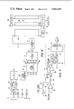
- FIG. 2 is a perspective illustration of the page width character scanning system of the invention
- FIG. 3 is a perspective illustration of the document illumination system used in conjunction with the invention.
- FIG. 4 is an illustrative schematic diagram of the self-scanned photocell arrays used in conjunction with the invention.
- FIG. 5A is a block diagram of a portion of one of the self-scanned photocell arrays used in the invention.
- FIG. 5B is a perspective illustration of an alternate embodiment of a self-scanned photocell array used in the invention.
- FIG. 6 is a block diagram of the character scanning system of the invention.
- FIG. 7 is a schematic diagram of one of the integrating amplifiers and analog/digital converters used in the invention.
- FIG. 8 is a block diagram of the fixed pattern error correction circuitry used in the system of the invention.
- FIGS. 9 and 10a-10c are charts which serve to explain the operation of the circuitry of FIG. 8;
- FIG. 11 is a block diagram of the scan pattern error correction circuitry used in the system of the invention.
- FIG. 12 is a fragmented partial block diagram which serves to explain the operation of the circuitry of FIG. 11;
- FIG. 13 is a block diagram of the memory circuit used in the system of the invention.
- a document 17 having transversely extending lines of characters 18 is moved beneath the photocell scanner 12.
- the document 17 is transported in the direction of arrow 19 which is generally perpendicular to the lines of characters 18 being scanned.
- An image of a line of characters 18 extending across substantially the entire useful width of the document 17, is projected by means of a plurality of lenses 21-24 onto the photosensitive scanner 12 which may comprise four self-scanned photodiode arrays 25-28.
- Each of the lenses 21-24 view adjacent illuminated regions so that a complete line of characters 18 is projected onto the photodiode arrays 25-28.
- Each of the four arrays 25-28 may typically comprise 512 photodiodes to obtain a field of view of 2,048 resolution elements across a typical ten-inch page width.
- each of the arrays 25-28 include circuitry which, on command, scans the incident light level on each of the photodiodes and produces a train of output signals.
- the scanned outputs of each of the arrays 25-28 are passed through amplifiers and analog-to-digital converters 31-34 into pre-processing circuits 35-38.
- the pre-processing circuitry corrects fixed pattern errors in the photodiode outputs which are inherent in the scanning sensor and, in addition, corrects scan pattern offset in the data from the arrays and binary quantizes each output into either a black or a white decision.
- the pre-processed digital data is then stored in a line-by-line data memory 39 which has the capacity for storing approximately two complete lines of character images.
- a linetracking circuit 40 follows the data through the memory 39 so that a complete line of data may be located within the memory. The data is shifted out of the memory 39 to a recognition unit for character identification.
- FIG. 3 it can be seen how each individual line of data is illuminated and scanned by the page width photodiode array used in the invention.
- a pair of elongate incandescent lamps 41 are mounted coaxially with semi-cylindrical reflectors 14 and 15 which project light from the lamps 41 into a narrow strip to form an elongate illuminated region 43 on the surface of the document 17.
- the illuminated region 43 is in alignment with the field of view of the sensor and extends parallel to the character lines 18 and perpendicular to the direction of document movement, shown by arrow 19.
- FIG. 5A A portion of the internal structure of each of the photodiode arrays is shown schematically in FIG. 5A.
- Each one of the photodiodes in the columnar array 52 is connected to a video line 55a or 55b through an MOS field effect isolation transistor 56.
- the odd-numbered group of photodiodes are connected to one video line while the even-numbered group of photodiodes are connected to the other.
- an enable bit is stepped along each of two 256-stage dynamic shift registers 58 and 59 to sequentially energize adjacent ones of the isolation transistors 56.
- the odd-numbered group of photodiode elements are accessed through one shift register and the even-numbered group of elements are accessed through the other shift register.
- an enable bit 57c is moved along shift register 58 and output photodiode data is produced on video line 55a.
- An array may be scanned by alternately pulsing the clock lines 57a and 57b so that the video lines 55a and 55b may be tied together to produce one common train of signals.
- the clock lines 57a and 57b may be pulsed simultaneously and one group of data collected from each of the separate video lines 55a and 55b.
- the photodiodes in each array operate in a charge storage mode, i.e., the array is scanned with each diode being sequentially accessed and charged through a common video line to a standard voltage value. During the scan period, the diodes are discharged by the photo current generated by incident light. The charge required to restore each diode in sequence to the standard voltage is the video output signal. As illustrated in FIG. 5A, the diodes are accessed by dynamic shift registers integrated onto the same silicon chip. As each diode is sampled, it is charged through the video line.
- the output on each scan is two trains of 256 pulses, each with an amplitude proportional to the spatial variation in light intensity across the array.
- FIG. 6 is a block diagram of the page width optical character processing system of the present invention.
- the four lenses 21-24 are arranged to intercept adjacent regions of an entire line of characters on the surface of the document 17. An image of the character line is projected through the lenses 21-24 onto the surface of the four self-scanned photocell arrays 25-28.
- two output channels 61 and 62 are coupled, respectively, to the input terminals of two integrating amplifiers 63 and 64.
- the odd-numbered photodiode elements are sampled and output on line 61 simultaneously with the even-numbered photodiode elements which are sampled and output on line 62.
- signals may be processed at a very high scan rate since each of the two video amplifiers 63 and 64 are only required to operate at half the actual rate of scanning the diodes in the array 28.
- the outputs of the analog-to-digital converters 65 and 66 are input to a 2:1 multiplex unit 67 which arranges the two streams of five-bit words into a single serial stream of five-bit words.
- the words output from the two converters are arranged alternately so that the single serial stream output is in the same order as if the diode array 28 had been scanned to produce a single channel output rather than the two channels 61 and 62.
- the output of the multiplex unit 67 is connected to the input of an error correction circuit 68 wherein each one of the 5-bit words in the serial data stream is corrected to eliminate fixed pattern errors.
- the serial data stream of 5-bit words from the error correction circuitry 68 is indicative of the corrected photocell gray level values and is input to a scan pattern error correction circuit 69. After scan pattern correction, the data are input to a 4:1 multiplex unit 76 over channels 81, 82, 83 and 84.
- the multiplexed single stream of 5-bit data words is passed from the multiplex unit 76 via channel 71 into a binary quantization unit 72 wherein a black or white decision is made for each cell value.
- the output data from the binary quantization unit 72 comprises a serial stream of single-bit data words indicating either a black condition or a white condition for each photodiode in the array 28.
- Data from photocell arrays 25, 26 and 27 are processed in a manner identical to that explained above in connection with photocell array 28.
- the output data trains are input over channel 81, 82, 83 and 84 into the multiplex unit 76, wherein the four channels are combined into a single channel 71 in the same sequence as the photocell arrays 25-28.
- the output of the multiplex unit 76 is transmitted over channel 71 to the binary quantization circuit 72 and then via channel 73 to a video buffer memory unit 86.
- the video buffer memory 86 stores successive page width scans sufficient to encompass a page width line of characters even though the line might be slightly skewed on the page.
- the data within the memory 86 is examined by a line tracking logic unit 87 which gates lines of characters alternately into either of two line buffer registers 88 and 89.
- a line tracking logic unit 87 which gates lines of characters alternately into either of two line buffer registers 88 and 89.
- data from the buffer memory 86 is transmitted over channel 91 through input gating circuitry 92 so that complete lines of characters are input.
- the registers 88 and 89 are alternately loaded and unloaded so that data is written into register 88 while data is simultaneously output from register 89. This enables the system to operate continuously at the scanning frequency.
- the feature recognition unit may be of several different types well known in the art.
- the integrating amplifier 63 and the analog-to-digital converters 65 are shown schematically in FIG. 7.
- Data from a self-scanned photocell array is input over a single channel 101 to a high gain operational amplifier 102.
- An integrating capacitor 103 is connected in a feedback configuration from the output of the operational amplifier 102 to the input lead 101.
- a pair of MOS field effect transistors 105 are connected across the capacitor 103, through a resistor 104, to reset the circuit for each pulse to be processed. Dual transistors are employed for increased reset stability. Thus, the transistors 105 are provided with a train of reset signals over line 106.
- Each of the level detectors 115 is connected to logic circuitry 116.
- the analog-to-digital converter 110 receives a series of pulses of varying amplitude and generates a five-bit digital word for each pulse.
- the A/D converter 110 can generate any one of 32 five-bit words indicative of the grey level of an input pulse and deliver a train of words at the scanning frequency over path 117 as its output signal.
- pulses of analog video data comprising current waveforms are input to the circuitry of FIG. 7 over line 101 and a five-bit digital representation of the pulses is obtained over line 117.
- the photocurrent-time average is obtained for the sampled regions of each of the characters.
- FIG. 8 is a block diagram illustrating the arrangement and function of the error correction circuits employed in the invention to eliminate fixed pattern errors in the photocell outputs.
- FIG. 8 shows a typical photodiode array 201 including a column of n photodiodes 202 and the associated gating and shift counter circuitry 203.
- the illumination values of the n photocells are sampled and sequentially passed through an integrating amplifier 204, an analog-to-digital converter 205, and into a steering logic unit 206.
- the steering logic unit 206 acting in response to signals over path 208 from a controller 207, directs data from the analog-to-digital converter 205 to either a reference subtractor unit 211, via path 210a, or to a code subtractor unit 212, via path 210b.
- black reference signals R b (n) from a system control computer, are input to the reference subtractor 211 in response to signals over path 213 from the controller 207.
- the difference signals produced by the subtractor 211 are "black codes" C b (n) and are delivered over path 214 to a black code storage register 215.
- Each black code signal C b (n) is input to an individual storage stage of the storage registers 215 in response to signals from the controller 207 over path 216.
- the register 215 comprises a recirculating shift register of a capacity sufficient to store at least n five-bit codes, one code for each of the n individual photodiodes in the array 201.
- the white codes stored in register 226 are passed, via path 228, to the multiplier unit 222.
- the output of the multiplier 222 is in turn connected to a multiply-by-two circuit 229, the output of which is corrected video R v (n) which is delivered to the binary quantization circuit 69 of FIG. 6 for further processing.
- the function of the circuitry of FIG. 8 is to process a serial stream of five-bit video data from an analog-to-digital converter and provide a corrected video signal R v (n) output which has been corrected cell-by-cell for fixed pattern errors, such as clock noise in the system, non-uniform document illumination, individual light response differences in photocells, lens vignetting, etc.
- R v (n) corrected video signal
- the black code storage register 215 there are stored n words (equal to the number of photodiodes per channel) of five bits each. Each black code word enables compensation of its associate photocell output for fixed pattern errors which are independent of illumination, for example, that due to clock noise.
- the error correction circuitry should be calibrated.
- a uniformly "black” document is passed through the sensor field of view and an execute black code signal EXBC is applied to the controller 207.
- a uniformly "white” document is passed through the sensor field of view and an execute white code command signal EXWC is applied to the controller 207.
- the steering logic path 210b is selected and an apparent white reflectance signal R' w (n) is fed to the subtractor 212 to produce an output difference signal R' w (n) - C b (n) which is delivered to the divider unit 224.
- the white reference value R w (n) from the system control computer is divided by 2 in divider 225 for circuit design reasons and also input to the divider unit 224.
- the quotient from divider 224 is a white code signal C w (n) formed by the operation: ##EQU1##
- the white code signal for each of the n photocells is stored in the respective stages of the white code storage register 226.
- a process video data signal PVD is delivered from the system control computer to the controller 207.
- Data from a document having characters thereon to be analyzed is gathered by scanning the photocells in the array 202, passing the data to the integrating amplifier 204, theanalog-to-digital converter 205 and to the steering logic circuitry 206.
- the uncorrected video data R' v (n) is input on a cell-by-cell basis to the code subtractor unit 212.
- the data from the corresponding stages of the black code storage register 215 is also input in synchronism to the code subtractor unit 212 via channel 217 under control of the controller 207.
- the theory behind correction for fixed pattern errors is that first the non-illumination-related errors are first removed from the data by subtracting the black code. Next, the illumination-related error, which is proportional to the white reference divided by the white data minus the black, is removed by multiplying the uncorrected data by the proportion factor.
- FIG. 9 is a table of exemplary sets of data values which might be calculated for each photocell and used by the circuitry of FIG. 8.
- the apparent black signal, R' b (1) obtained when a black standard documen is passed beneath the scanner, is 00011.
- the black reference value, R b (1) is selected to be 00000 for each photocell.
- the value R' w (1) - C b (1) is calculated as 10110.
- the white code factor C w (n) which is divided first by two for logic design purposes, is 10101.
- the actual corrected white value R w (1), calculated by the circuitry of FIG. 8, is therefore equal to 11101.
- FIGS. 10a, 10b and 10c are a set of three graphs which illustrate signal values for both black and white test references (FIG. 10a); apparent video signal values directly from the photocell scanner (FIG. 10b); and the corrected video output signal from the error correction circuitry (FIG. 10c).
- the signal pattern 301 is obtained as an output from the first 13 photocells of the array when a black test document is moved beneath the array.
- the data in the pattern 301 alternates in an odd-even pattern, and represents error due primarily to clock noise.
- the data obtained from the white reference test is shown in signal pattern 302.
- the white reference value selected, R w (n), is 11101, while the black reference, R b (n) is selected as 00000.
- FIG. 11 is a block diagram illustrating the arrangement and function of the scan pattern error correction circuit employed in the invention to eliminate scan offset errors in the photocell output pattern.
- Data from each of the fixed pattern error correction circuits 68 is output to one of four channels 501-504, respectively.
- Data on channel 501 is passed directly into a first video buffer memory 505.
- Data on channel 502 is coupled to the input of a first scan delay shift register 509, the output of which is connected to a second video buffer memory 506.
- Channel 503 is connected to the input of two series connected scan delay shift registers 510 and 511, output of which is connected to a third scan video buffer memory 507.
- Channel 504 is connected to the input of three series connected scan delay shift registers 512, 513 and 514 the output of which is coupled to a fourth video buffer memory 508.
- the respective outputs of the four video buffer memories 505- 508 are connected via channels 515-518 to the inputs of the 4:1 multiplex unit 76.
- the first buffer memory 505 includes input steering gates 521, output steering gates 522 and a pair of buffer storage registers 523a and 523b.
- the steering gates 521 and 522 are operated by a load/unload control unit 524 to alternately load registers 523a and 523b.
- the buffer memories 505-508 enable data from the fixed pattern error correction circuits 68 to be loaded into one of the two registers, 523a or 523b, at the same time data is being unloaded from the other register and passed over channels 515-518 to the 4:1 multiplex unit 76.
- each one of the four 512 element arrays are scanned simultaneously in the same direction.
- the time required to scan an array may be on the order of 200 to 400 microseconds with 256 microseconds being a scanning rate used in one embodiment. Since documents are in motion during scanning the particular document area in alignment with the last element in one array is offset slightly from the area in alignment with the first element in the next adjacent array. For example, with typical document speeds and scanning rates the offset may be on the order of four mils.
- the data from each scan are preferably corrected to eliminate the offset and produce a scanned data pattern wherein all of the data are aligned in a single columnar pattern prior to recognition processing.
- the initial scan pattern from the four 512 element arrays is segmented, as shown in area 531. That is, the end portions of adjacent arrays are offset from one another. For example, there is an offset, designated by character 532, between the data from cell 511a and data from cell 0b.
- the preferred scan pattern configuration is one wherein the data from each of the cells in all four of the arrays are essentially axially aligned in a single columnar pattern.
- Scan correction is accomplished by providing the series of delaying shift registers 509-514 to delay the data from each scan for a preselected period and thereby compensate for the scan offset.
- Each of the registers 509-514 comprises a dynamic shift register having a storage capacity of 512 words comprising four to five bits per word.
- Each register is driven at the clock rate so that the time required to shift a particular data word through one register is the equivalent of one column delay and compensates for the offset between adjacent columns. That is, the first group of data over channel 501, does not incorporate any delay at all.
- the second group of data, from channel 502, is delayed for one column by passage through shift register 509.
- the third group of data, on channel 503, is delayed for two columns by shifting through two series connected shift registers 510 and 511.
- the fourth group of data on channel 504 is delayed for three columns by shifting through series connected registers 512, 513 and 514. Passage through the groups of serial shift registers produces data outputs which have been delayed sufficiently to realign each of the scans so that the adjacent ends of contiguous scans are shifted the amount of its offset from the data of the undelayed scan.
- data is input to the four video buffer memories 505-508 at the clock rate ⁇ .
- the video buffer memories enable data to be loaded into a register at the clock rate and unloaded from a register at 4 ⁇ , four times the clock rate.
- the memories are controlled so that there is an alternating sequence of (1) load register a at the clock rate ⁇ and simultaneously unload the contents of register b at 4 ⁇ ; and (2) load register b at the clock rate ⁇ while simultaneously unloading register a at 4 ⁇ .
- the output data from the steering gates of each of the video buffer memories 505-508 is input to the 4:1 multiplex unit 76.
- the output of the multiplex unit 76 over channel 71, comprises a corrected scan pattern as designated in area 534.
- the corrected scan pattern from each of the four 512 element arrays is now axially aligned into a signle 2,048 element column of data serially clocked at four times the clock rate, i.e., 4 ⁇ .
- Prior art page width processors have attempted scan pattern correction by tilting adjacent arrays to introduce an initial offset. These systems have encountered many accuracy and reliability difficulties. Moreover, as the length of scan is increased to inhance line resolution, the error factor due to scan offset is also increased.
- the scan pattern correction technique used in the circuitry of FIG. 11 substantially increases the accuracy of a page width scanning system, eliminates a substantial source of error, and thereby makes implementation of such a system practical.
- the scanned character data after both fixed pattern and scan pattern error correction, is multiplexed, binary quantized, and sent to the video memory circuitry shown in FIG. 13.
- the multiplexed data on path 401 is input to a primary video buffer 402 comprising an array of cascaded dynamic shift registers 403.
- each register 403 preferably has storage capacity for at least 2,048 bits (to accommodate data from four photodiode arrays of 512 bits each).
- the individual shift registers 403 are interconnected with one another via recirculation paths 404 to shift the data through the memory in a zig-zag fashion at the scanning rate.
- the shift registers 403 are preferably comprised of silicon gate MOS integrated circuit devices.
- the output of the storage element for word n provides input data for the word n+1 so that the memory contents are continuously shifted through the registers at a rate corresponding to the scanning frequency rate.
- the memory 402 has sufficient capacity for storage of a page width line of characters; the approximate area of a page being stored to allow for line skew being stored is 9 inches in width ⁇ 3/4 inch in height.
- Video memory word length and the number of words to be stored is fixed by the scanning resolution. For a preferred 4 mil ⁇ 4 mil document sampling, the memory is 2,048 bits per word and 192 words in height.
- the passage of data through the memory 402 is monitored by a line-tracking logic unit 405 via leads 406.
- the line-tracking logic unit 405 functions to monitor the data stored in memory 402 and includes the following elements:
- control signals are passed to a control-and-sequence circuit 410 over path 411, and an enable signal is applied over leads 412 to energize one of the two AND gates 413 and 414.
- the character data is then transmitted over line 415, through one of the two gates 413 or 414 and into one of two secondary buffer memories 416 and 417.
- the memories 416 and 417 are also comprised of a plurality of cascaded dynamic shift registers 418 and preferably include storage areas for 2,048 bits per register for 48 scans in height. Two memories are provided to permit processing of data at the scanning frequency. While one of the secondary buffer memories is being loaded with a line of characters from the primary video buffer memory 402, the other secondary buffer is being unloaded to recognition circuitry.
- the output interface circuitry 425 and the control-and-sequence circuit 410 remove the recirculate signal and apply a disable signal over path 421 to disable the gates 419 and 423. All of the stored data is then unloaded in parallel over paths 426 through the output interface circuitry and via channel 427 to the recognition unit. While the memory 416 is being dumped to the recognition unit, the next line of characters is being input to memory 417 through gate 414 in a manner identical to the loading of memory 416.
- the alternate loading and unloading of the secondary buffer memory units 416 and 417 from the primary buffer memory 402 enables the system to operate and continuously process data at the scanning frequency.
- buffer memories 402, 416 and 417 While cascaded dynamic shift registers are preferred for the buffer memories 402, 416 and 417, it is to be understood that other types of data storage systems might be used.
- these memories could comprise random access memories implemented with bipolar integrated memory chips.
- Data is entered bit-by-bit in single words, corresponding to a scan across a page, at random memory locations.
- This format of buffer memory is of particular interest with respect to formatted documents wherein the paper advance is controlled in order to place the data field to be read within the memory "field of view" thereby avoiding the complexity of a character line which is split; for example, where the memory field of view border falls along a character line.
- line tracking logic 405 must also include an address generation unit which provides sequential row-and-column research instructions to examine a group of bit locations from several parallel words.
- a further technique which may be employed for the buffer memories is that of charge-coupled register elements arranged in the same configuration as the cascaded dynamic MOS shift registers described above.
- Charge-coupled shift registers possess the advantages over MOS devices of greatly reduced costs and increased shift rates. Further, charge-coupled shift registers enable the inclusion of logic functions within the shift register elements to simplify line-tracking functions. Another advantage is inherent in the fact that charge-coupled shift registers can also store analog data whereas other techniques are restricted to digital data only.
Abstract
Description
n          photodiode cell number
R'.sub.b (n)
           apparent black value
R.sub.b (n)
           actual black value
C.sub.b (n)
           "code black" value which is equal
            to R'.sub.b (n) - R.sub.b (n)
R'.sub.w (n)
           apparent white value
R.sub.w (n)
           actual white value
C.sub.w (n)
           "white code" value
Claims (19)
Priority Applications (1)
| Application Number | Priority Date | Filing Date | Title |
|---|---|---|---|
| US05/264,014 US3962681A (en) | 1972-06-19 | 1972-06-19 | Page width optical character processing method and system |
Applications Claiming Priority (1)
| Application Number | Priority Date | Filing Date | Title |
|---|---|---|---|
| US05/264,014 US3962681A (en) | 1972-06-19 | 1972-06-19 | Page width optical character processing method and system |
Publications (1)
| Publication Number | Publication Date |
|---|---|
| US3962681A true US3962681A (en) | 1976-06-08 |
Family
ID=23004197
Family Applications (1)
| Application Number | Title | Priority Date | Filing Date |
|---|---|---|---|
| US05/264,014 Expired - Lifetime US3962681A (en) | 1972-06-19 | 1972-06-19 | Page width optical character processing method and system |
Country Status (1)
| Country | Link |
|---|---|
| US (1) | US3962681A (en) |
Cited By (69)
| Publication number | Priority date | Publication date | Assignee | Title |
|---|---|---|---|---|
| US4044384A (en) * | 1975-07-24 | 1977-08-23 | Ricoh Co., Ltd. | Optical scanning apparatus |
| US4057845A (en) * | 1975-04-09 | 1977-11-08 | Hitachi, Ltd. | Group control system for visual information processing |
| US4080633A (en) * | 1976-07-15 | 1978-03-21 | Xerox Corporation | Twisting geometry scanner |
| US4084153A (en) * | 1976-03-15 | 1978-04-11 | Harris Corporation | Apparatus for reconstructing a binary bit pattern |
| US4092632A (en) * | 1977-05-02 | 1978-05-30 | Xerox Corporation | Crossover arrangement for multiple scanning arrays |
| US4128830A (en) * | 1977-09-26 | 1978-12-05 | International Business Machines Corporation | Apparatus for providing a compensation signal for individual light sensors arranged in a predetermined relation |
| US4129853A (en) * | 1977-09-26 | 1978-12-12 | International Business Machines Corporation | Method and apparatus for producing compensated signals for individual light sensors arranged in a predetermined relation |
| US4147928A (en) * | 1977-05-02 | 1979-04-03 | Xerox Corporation | Scanning array configuration |
| US4157533A (en) * | 1977-11-25 | 1979-06-05 | Recognition Equipment Incorporated | Independent channel automatic gain control for self-scanning photocell array |
| US4158834A (en) * | 1977-04-06 | 1979-06-19 | Shinko Electric Co., Ltd. | Data buffer for a label reader system including a data processor |
| US4199784A (en) * | 1975-04-25 | 1980-04-22 | Dr. Ing. Rudolf Hell Gmbh | Method and apparatus for electro-optically recording pictorial information for a facsimile transmission system |
| US4203136A (en) * | 1975-04-25 | 1980-05-13 | Dr. Ing. Rudolf Hell Gmbh | Method and apparatus for electro-optically sensing, transmitting and recording pictorial information in particular facsimile transmission systems |
| US4216503A (en) * | 1979-03-26 | 1980-08-05 | Xerox Corporation | Signal restoration and gain control for image viewing devices |
| US4240118A (en) * | 1975-04-25 | 1980-12-16 | Dr. Ing. Rudolf Hell Gmbh | Method for electro-optically sensing, transmitting pictorial information |
| US4240117A (en) * | 1976-04-21 | 1980-12-16 | Dr. Ing. Rudolf Hell Gmbh | Apparatus for electro-optically recording pictorial information for a facsimile transmission system |
| US4246606A (en) * | 1979-04-17 | 1981-01-20 | Hajime Industries Ltd. | Inspection apparatus |
| US4249217A (en) * | 1979-05-29 | 1981-02-03 | International Business Machines Corporation | Separated sensor array abutment |
| US4268870A (en) * | 1978-04-28 | 1981-05-19 | Canon Kabushiki Kaisha | Recording apparatus for reading information from an original |
| US4272756A (en) * | 1978-05-22 | 1981-06-09 | Hitachi, Ltd. | Method of pattern recognition and apparatus thereof |
| EP0031728A2 (en) * | 1979-12-31 | 1981-07-08 | Ncr Canada Ltd - Ncr Canada Ltee | Method and apparatus for electronically aligning active elements of an imaging array with an optical system |
| US4292621A (en) * | 1978-08-14 | 1981-09-29 | Paul Fuller | Character reader |
| US4295121A (en) * | 1979-01-16 | 1981-10-13 | International Business Machines Corporation | Device for optical character reading |
| FR2487613A1 (en) * | 1980-07-24 | 1982-01-29 | Matra | DEVICE FOR READING OR RETRIEVING A DOCUMENT, IN PARTICULAR FOR A TELEPHONE DEVICE |
| US4314281A (en) * | 1979-10-12 | 1982-02-02 | Xerox Corporation | Shading compensation for scanning apparatus |
| US4318135A (en) * | 1979-10-12 | 1982-03-02 | Xerox Corporation | Alignment system for scanning arrays |
| US4348593A (en) * | 1981-01-29 | 1982-09-07 | Xerox Corporation | Twisting geometry optical system utilizing imaging array with time delay segments |
| US4370641A (en) * | 1979-08-15 | 1983-01-25 | International Business Machines Corporation | Electronic control system |
| US4383275A (en) * | 1979-09-29 | 1983-05-10 | Sharp Kabushiki Kaisha | Read-out level compensation in an optical reader system |
| US4402087A (en) * | 1979-07-20 | 1983-08-30 | Sumitomo Electric Industries, Ltd. | Binary coding circuit |
| EP0099229A2 (en) * | 1982-07-08 | 1984-01-25 | Mitsubishi Rayon Co., Ltd. | Image measuring system |
| US4433346A (en) * | 1982-03-31 | 1984-02-21 | Xerox Corporation | Raster input scanner |
| US4453268A (en) * | 1981-03-18 | 1984-06-05 | Lundy Electronics & Systems, Inc. | OCR Page reader |
| US4496984A (en) * | 1982-11-18 | 1985-01-29 | Xerox Corporation | Raster input/output scanner |
| US4506301A (en) * | 1979-10-12 | 1985-03-19 | Xerox Corporation | Multiple mode raster scanner |
| US4515275A (en) * | 1982-09-30 | 1985-05-07 | Pennwalt Corporation | Apparatus and method for processing fruit and the like |
| US4535359A (en) * | 1983-01-17 | 1985-08-13 | Eastman Kodak Company | Defect correction in solid state imaging |
| US4583126A (en) * | 1982-11-18 | 1986-04-15 | Xerox Corporation | Raster input/output scanner |
| US4672186A (en) * | 1981-10-01 | 1987-06-09 | Banctec Inc. | Digital document scanning system |
| US4677683A (en) * | 1984-05-11 | 1987-06-30 | Skantek Corporation | System for correcting errors in the dimensional location of fibers in _an optical fiber scanning head |
| US4736251A (en) * | 1982-12-15 | 1988-04-05 | Ikegami Tsushinki Co. Ltd. | Color image pickup apparatus having one or more line sensors and a mechanical sub-scanning device |
| US4811410A (en) * | 1986-12-08 | 1989-03-07 | American Telephone And Telegraph Company | Linescan inspection system for circuit boards |
| US4929845A (en) * | 1989-02-27 | 1990-05-29 | At&T Bell Laboratories | Method and apparatus for inspection of substrates |
| US4984285A (en) * | 1987-08-26 | 1991-01-08 | Hitachi, Ltd. | Method of correcting shading phenomenon in optical character reader |
| US5097516A (en) * | 1991-02-28 | 1992-03-17 | At&T Bell Laboratories | Technique for illuminating a surface with a gradient intensity line of light to achieve enhanced two-dimensional imaging |
| US5140647A (en) * | 1989-12-18 | 1992-08-18 | Hitachi, Ltd. | Image joining method and system |
| US5144448A (en) * | 1990-07-31 | 1992-09-01 | Vidar Systems Corporation | Scanning apparatus using multiple CCD arrays and related method |
| US5153929A (en) * | 1990-03-31 | 1992-10-06 | Canon Kabushiki Kaisha | Image reading apparatus outputting corrected image signals |
| EP0558936A2 (en) * | 1992-01-31 | 1993-09-08 | Mita Industrial Co. Ltd. | An image reading device |
| US5430550A (en) * | 1991-06-14 | 1995-07-04 | Minolta Camera Kabushiki Kaisha | Image reading apparatus which corrects for positional and angular deviation between the image sensor and the document |
| US5675672A (en) * | 1990-06-26 | 1997-10-07 | Seiko Epson Corporation | Two dimensional linker for character string data |
| US5793904A (en) * | 1995-12-06 | 1998-08-11 | Minnesota Mining And Manufacturing Company | Zoned inspection system and method for presenting temporal multi-detector output in a spatial domain |
| EP1133147A2 (en) * | 2000-01-04 | 2001-09-12 | Hewlett-Packard Company, A Delaware Corporation | Optical assembly having a reduced width |
| US6535617B1 (en) * | 2000-02-14 | 2003-03-18 | Digimarc Corporation | Removal of fixed pattern noise and other fixed patterns from media signals |
| US20050117776A1 (en) * | 1992-07-31 | 2005-06-02 | Digimarc Corporation | Image marking adapted to the image |
| US7185103B1 (en) * | 2002-09-10 | 2007-02-27 | Juniper Networks, Inc. | Rate-controlled transmission of traffic flow information |
| US7251215B1 (en) | 2002-08-26 | 2007-07-31 | Juniper Networks, Inc. | Adaptive network router |
| US7254114B1 (en) | 2002-08-26 | 2007-08-07 | Juniper Networks, Inc. | Network router having integrated flow accounting and packet interception |
| US7313100B1 (en) | 2002-08-26 | 2007-12-25 | Juniper Networks, Inc. | Network device having accounting service card |
| US7420929B1 (en) | 2002-07-02 | 2008-09-02 | Juniper Networks, Inc. | Adaptive network flow analysis |
| US7546635B1 (en) | 2004-08-11 | 2009-06-09 | Juniper Networks, Inc. | Stateful firewall protection for control plane traffic within a network device |
| US7633944B1 (en) | 2006-05-12 | 2009-12-15 | Juniper Networks, Inc. | Managing timeouts for dynamic flow capture and monitoring of packet flows |
| US20100071024A1 (en) * | 2008-09-12 | 2010-03-18 | Juniper Networks, Inc. | Hierarchical application of security services within a computer network |
| US7747737B1 (en) | 2006-05-12 | 2010-06-29 | Juniper Networks, Inc. | Network device having service card for dynamic flow capture and monitoring of packet flows |
| US8307030B1 (en) | 2010-04-20 | 2012-11-06 | Juniper Networks, Inc. | Large-scale timer management |
| US8339959B1 (en) | 2008-05-20 | 2012-12-25 | Juniper Networks, Inc. | Streamlined packet forwarding using dynamic filters for routing and security in a shared forwarding plane |
| US8369345B1 (en) | 2009-11-13 | 2013-02-05 | Juniper Networks, Inc. | Multi-router system having shared network interfaces |
| US9246828B1 (en) | 2014-06-18 | 2016-01-26 | Juniper Networks, Inc. | Traffic-aware sampling rate adjustment within a network device |
| US9251535B1 (en) | 2012-01-05 | 2016-02-02 | Juniper Networks, Inc. | Offload of data transfer statistics from a mobile access gateway |
| US9485149B1 (en) | 2004-01-06 | 2016-11-01 | Juniper Networks, Inc. | Routing device having multiple logical routers |
Citations (8)
| Publication number | Priority date | Publication date | Assignee | Title |
|---|---|---|---|---|
| US3159815A (en) * | 1961-11-29 | 1964-12-01 | Ibm | Digitalization system for multi-track optical character sensing |
| US3234327A (en) * | 1961-03-31 | 1966-02-08 | Columbia Broadcasting Syst Inc | High-resolution scanning system having low-resolution components |
| US3293415A (en) * | 1962-12-03 | 1966-12-20 | Ibm | Data processing input apparatus |
| US3475555A (en) * | 1966-04-22 | 1969-10-28 | Columbia Broadcasting Syst Inc | Dual resolution scanning system using carrier transmission of plural video signals |
| US3582884A (en) * | 1968-01-30 | 1971-06-01 | Cognitronics Corp | Multiple-scanner character reading system |
| US3651462A (en) * | 1970-07-20 | 1972-03-21 | Ibm | Single scan character registration |
| US3697682A (en) * | 1971-06-11 | 1972-10-10 | Bell Telephone Labor Inc | Video signal processing |
| US3717848A (en) * | 1970-06-02 | 1973-02-20 | Recognition Equipment Inc | Stored reference code character reader method and system |
-
1972
- 1972-06-19 US US05/264,014 patent/US3962681A/en not_active Expired - Lifetime
Patent Citations (8)
| Publication number | Priority date | Publication date | Assignee | Title |
|---|---|---|---|---|
| US3234327A (en) * | 1961-03-31 | 1966-02-08 | Columbia Broadcasting Syst Inc | High-resolution scanning system having low-resolution components |
| US3159815A (en) * | 1961-11-29 | 1964-12-01 | Ibm | Digitalization system for multi-track optical character sensing |
| US3293415A (en) * | 1962-12-03 | 1966-12-20 | Ibm | Data processing input apparatus |
| US3475555A (en) * | 1966-04-22 | 1969-10-28 | Columbia Broadcasting Syst Inc | Dual resolution scanning system using carrier transmission of plural video signals |
| US3582884A (en) * | 1968-01-30 | 1971-06-01 | Cognitronics Corp | Multiple-scanner character reading system |
| US3717848A (en) * | 1970-06-02 | 1973-02-20 | Recognition Equipment Inc | Stored reference code character reader method and system |
| US3651462A (en) * | 1970-07-20 | 1972-03-21 | Ibm | Single scan character registration |
| US3697682A (en) * | 1971-06-11 | 1972-10-10 | Bell Telephone Labor Inc | Video signal processing |
Non-Patent Citations (3)
| Title |
|---|
| Crawford, "Pictorial Information Disector and Analyzer System," IBM Tech. Disclosure Bulletin, vol. 15, No. 1, June 1972, pp. 61 & 62. * |
| Salsbury et al., "A Monolithic Image Sensor . . . ," Proceedings of the IEEE, vol. 58, No. 9, Sept. 1970, pp. 1302-1305. * |
| Swart, "Contrast Amplifier," IBM Tech. Disclosure Bulletin, vol. 14, No. 3, Aug. 1971, pp. 883-884. * |
Cited By (92)
| Publication number | Priority date | Publication date | Assignee | Title |
|---|---|---|---|---|
| US4057845A (en) * | 1975-04-09 | 1977-11-08 | Hitachi, Ltd. | Group control system for visual information processing |
| US4240118A (en) * | 1975-04-25 | 1980-12-16 | Dr. Ing. Rudolf Hell Gmbh | Method for electro-optically sensing, transmitting pictorial information |
| US4203136A (en) * | 1975-04-25 | 1980-05-13 | Dr. Ing. Rudolf Hell Gmbh | Method and apparatus for electro-optically sensing, transmitting and recording pictorial information in particular facsimile transmission systems |
| US4199784A (en) * | 1975-04-25 | 1980-04-22 | Dr. Ing. Rudolf Hell Gmbh | Method and apparatus for electro-optically recording pictorial information for a facsimile transmission system |
| US4044384A (en) * | 1975-07-24 | 1977-08-23 | Ricoh Co., Ltd. | Optical scanning apparatus |
| US4084153A (en) * | 1976-03-15 | 1978-04-11 | Harris Corporation | Apparatus for reconstructing a binary bit pattern |
| US4240117A (en) * | 1976-04-21 | 1980-12-16 | Dr. Ing. Rudolf Hell Gmbh | Apparatus for electro-optically recording pictorial information for a facsimile transmission system |
| US4080633A (en) * | 1976-07-15 | 1978-03-21 | Xerox Corporation | Twisting geometry scanner |
| US4158834A (en) * | 1977-04-06 | 1979-06-19 | Shinko Electric Co., Ltd. | Data buffer for a label reader system including a data processor |
| US4092632A (en) * | 1977-05-02 | 1978-05-30 | Xerox Corporation | Crossover arrangement for multiple scanning arrays |
| US4147928A (en) * | 1977-05-02 | 1979-04-03 | Xerox Corporation | Scanning array configuration |
| US4129853A (en) * | 1977-09-26 | 1978-12-12 | International Business Machines Corporation | Method and apparatus for producing compensated signals for individual light sensors arranged in a predetermined relation |
| US4128830A (en) * | 1977-09-26 | 1978-12-05 | International Business Machines Corporation | Apparatus for providing a compensation signal for individual light sensors arranged in a predetermined relation |
| FR2410394A1 (en) * | 1977-11-25 | 1979-06-22 | Recognition Equipment Inc | INDEPENDENT CHANNEL AUTOMATIC GAIN CONTROL DEVICE FOR A SELF-ANALYZED PHOTO-ELECTRIC CELL MATRIX |
| US4157533A (en) * | 1977-11-25 | 1979-06-05 | Recognition Equipment Incorporated | Independent channel automatic gain control for self-scanning photocell array |
| US4268870A (en) * | 1978-04-28 | 1981-05-19 | Canon Kabushiki Kaisha | Recording apparatus for reading information from an original |
| US4272756A (en) * | 1978-05-22 | 1981-06-09 | Hitachi, Ltd. | Method of pattern recognition and apparatus thereof |
| US4292621A (en) * | 1978-08-14 | 1981-09-29 | Paul Fuller | Character reader |
| US4295121A (en) * | 1979-01-16 | 1981-10-13 | International Business Machines Corporation | Device for optical character reading |
| US4216503A (en) * | 1979-03-26 | 1980-08-05 | Xerox Corporation | Signal restoration and gain control for image viewing devices |
| US4246606A (en) * | 1979-04-17 | 1981-01-20 | Hajime Industries Ltd. | Inspection apparatus |
| US4249217A (en) * | 1979-05-29 | 1981-02-03 | International Business Machines Corporation | Separated sensor array abutment |
| US4402087A (en) * | 1979-07-20 | 1983-08-30 | Sumitomo Electric Industries, Ltd. | Binary coding circuit |
| US4370641A (en) * | 1979-08-15 | 1983-01-25 | International Business Machines Corporation | Electronic control system |
| US4383275A (en) * | 1979-09-29 | 1983-05-10 | Sharp Kabushiki Kaisha | Read-out level compensation in an optical reader system |
| US4506301A (en) * | 1979-10-12 | 1985-03-19 | Xerox Corporation | Multiple mode raster scanner |
| US4314281A (en) * | 1979-10-12 | 1982-02-02 | Xerox Corporation | Shading compensation for scanning apparatus |
| US4318135A (en) * | 1979-10-12 | 1982-03-02 | Xerox Corporation | Alignment system for scanning arrays |
| EP0031728A2 (en) * | 1979-12-31 | 1981-07-08 | Ncr Canada Ltd - Ncr Canada Ltee | Method and apparatus for electronically aligning active elements of an imaging array with an optical system |
| EP0031728A3 (en) * | 1979-12-31 | 1984-10-24 | Ncr Canada Ltd - Ncr Canada Ltee | Method and apparatus for electronically aligning active elements of an imaging array with an optical system |
| EP0045252A2 (en) * | 1980-07-24 | 1982-02-03 | Matra | Document reading or reproducing device, in particular for a telecopying apparatus |
| EP0045252A3 (en) * | 1980-07-24 | 1982-02-10 | Matra | Document reading or reproducing device, in particular for a telecopying apparatus |
| WO1982000393A1 (en) * | 1980-07-24 | 1982-02-04 | Robbe M | Device for the reading or restoration of a document,particularly for a facsimile apparatus |
| FR2487613A1 (en) * | 1980-07-24 | 1982-01-29 | Matra | DEVICE FOR READING OR RETRIEVING A DOCUMENT, IN PARTICULAR FOR A TELEPHONE DEVICE |
| US4348593A (en) * | 1981-01-29 | 1982-09-07 | Xerox Corporation | Twisting geometry optical system utilizing imaging array with time delay segments |
| US4453268A (en) * | 1981-03-18 | 1984-06-05 | Lundy Electronics & Systems, Inc. | OCR Page reader |
| US4672186A (en) * | 1981-10-01 | 1987-06-09 | Banctec Inc. | Digital document scanning system |
| US4433346A (en) * | 1982-03-31 | 1984-02-21 | Xerox Corporation | Raster input scanner |
| EP0099229A3 (en) * | 1982-07-08 | 1985-12-18 | Mitsubishi Rayon Co., Ltd. | Image measuring system |
| EP0099229A2 (en) * | 1982-07-08 | 1984-01-25 | Mitsubishi Rayon Co., Ltd. | Image measuring system |
| US4515275A (en) * | 1982-09-30 | 1985-05-07 | Pennwalt Corporation | Apparatus and method for processing fruit and the like |
| US4496984A (en) * | 1982-11-18 | 1985-01-29 | Xerox Corporation | Raster input/output scanner |
| US4583126A (en) * | 1982-11-18 | 1986-04-15 | Xerox Corporation | Raster input/output scanner |
| US4736251A (en) * | 1982-12-15 | 1988-04-05 | Ikegami Tsushinki Co. Ltd. | Color image pickup apparatus having one or more line sensors and a mechanical sub-scanning device |
| US4535359A (en) * | 1983-01-17 | 1985-08-13 | Eastman Kodak Company | Defect correction in solid state imaging |
| US4677683A (en) * | 1984-05-11 | 1987-06-30 | Skantek Corporation | System for correcting errors in the dimensional location of fibers in _an optical fiber scanning head |
| US4811410A (en) * | 1986-12-08 | 1989-03-07 | American Telephone And Telegraph Company | Linescan inspection system for circuit boards |
| US4984285A (en) * | 1987-08-26 | 1991-01-08 | Hitachi, Ltd. | Method of correcting shading phenomenon in optical character reader |
| US4929845A (en) * | 1989-02-27 | 1990-05-29 | At&T Bell Laboratories | Method and apparatus for inspection of substrates |
| US5140647A (en) * | 1989-12-18 | 1992-08-18 | Hitachi, Ltd. | Image joining method and system |
| US5153929A (en) * | 1990-03-31 | 1992-10-06 | Canon Kabushiki Kaisha | Image reading apparatus outputting corrected image signals |
| US5675672A (en) * | 1990-06-26 | 1997-10-07 | Seiko Epson Corporation | Two dimensional linker for character string data |
| US5144448A (en) * | 1990-07-31 | 1992-09-01 | Vidar Systems Corporation | Scanning apparatus using multiple CCD arrays and related method |
| US5097516A (en) * | 1991-02-28 | 1992-03-17 | At&T Bell Laboratories | Technique for illuminating a surface with a gradient intensity line of light to achieve enhanced two-dimensional imaging |
| US5430550A (en) * | 1991-06-14 | 1995-07-04 | Minolta Camera Kabushiki Kaisha | Image reading apparatus which corrects for positional and angular deviation between the image sensor and the document |
| EP0558936A3 (en) * | 1992-01-31 | 1993-10-20 | Mita Industrial Co Ltd | An image reading device |
| US5436737A (en) * | 1992-01-31 | 1995-07-25 | Mita Industrial Co., Ltd. | Image reading device having a plurality of image sensors arranged in a main scanning direction and capable of producing continuous image data |
| EP0558936A2 (en) * | 1992-01-31 | 1993-09-08 | Mita Industrial Co. Ltd. | An image reading device |
| US20050117776A1 (en) * | 1992-07-31 | 2005-06-02 | Digimarc Corporation | Image marking adapted to the image |
| US7062070B2 (en) | 1992-07-31 | 2006-06-13 | Digimarc Corporation | Image marking adapted to the image |
| US5793904A (en) * | 1995-12-06 | 1998-08-11 | Minnesota Mining And Manufacturing Company | Zoned inspection system and method for presenting temporal multi-detector output in a spatial domain |
| EP1133147A2 (en) * | 2000-01-04 | 2001-09-12 | Hewlett-Packard Company, A Delaware Corporation | Optical assembly having a reduced width |
| EP1133147A3 (en) * | 2000-01-04 | 2002-08-07 | Hewlett-Packard Company, A Delaware Corporation | Optical assembly having a reduced width |
| US6535617B1 (en) * | 2000-02-14 | 2003-03-18 | Digimarc Corporation | Removal of fixed pattern noise and other fixed patterns from media signals |
| US8089895B1 (en) | 2002-07-02 | 2012-01-03 | Juniper Networks, Inc. | Adaptive network flow analysis |
| US7420929B1 (en) | 2002-07-02 | 2008-09-02 | Juniper Networks, Inc. | Adaptive network flow analysis |
| US7254114B1 (en) | 2002-08-26 | 2007-08-07 | Juniper Networks, Inc. | Network router having integrated flow accounting and packet interception |
| US7313100B1 (en) | 2002-08-26 | 2007-12-25 | Juniper Networks, Inc. | Network device having accounting service card |
| US7492713B1 (en) | 2002-08-26 | 2009-02-17 | Juniper Networks, Inc. | Adaptive network router |
| US7251215B1 (en) | 2002-08-26 | 2007-07-31 | Juniper Networks, Inc. | Adaptive network router |
| US7738396B1 (en) | 2002-08-26 | 2010-06-15 | Juniper Networks, Inc. | Network device having accounting service card |
| US7869352B1 (en) | 2002-08-26 | 2011-01-11 | Juniper Networks, Inc. | Adaptive network router |
| US7185103B1 (en) * | 2002-09-10 | 2007-02-27 | Juniper Networks, Inc. | Rate-controlled transmission of traffic flow information |
| US9832099B1 (en) | 2004-01-06 | 2017-11-28 | Juniper Networks, Inc. | Routing device having multiple logical routers |
| US9485149B1 (en) | 2004-01-06 | 2016-11-01 | Juniper Networks, Inc. | Routing device having multiple logical routers |
| US8020200B1 (en) | 2004-08-11 | 2011-09-13 | Juniper Networks, Inc. | Stateful firewall protection for control plane traffic within a network device |
| US7546635B1 (en) | 2004-08-11 | 2009-06-09 | Juniper Networks, Inc. | Stateful firewall protection for control plane traffic within a network device |
| US7633944B1 (en) | 2006-05-12 | 2009-12-15 | Juniper Networks, Inc. | Managing timeouts for dynamic flow capture and monitoring of packet flows |
| US8031715B1 (en) | 2006-05-12 | 2011-10-04 | Juniper Networks, Inc. | Network device having service card for dynamic flow capture and monitoring of packet flows |
| US8037175B1 (en) | 2006-05-12 | 2011-10-11 | Juniper Networks, Inc. | Network device having service card for intercept and monitoring of packet flows |
| US7809827B1 (en) | 2006-05-12 | 2010-10-05 | Juniper Networks, Inc. | Network device having service card for lawful intercept and monitoring of packet flows |
| US7747737B1 (en) | 2006-05-12 | 2010-06-29 | Juniper Networks, Inc. | Network device having service card for dynamic flow capture and monitoring of packet flows |
| US8339959B1 (en) | 2008-05-20 | 2012-12-25 | Juniper Networks, Inc. | Streamlined packet forwarding using dynamic filters for routing and security in a shared forwarding plane |
| US20100071024A1 (en) * | 2008-09-12 | 2010-03-18 | Juniper Networks, Inc. | Hierarchical application of security services within a computer network |
| US8955107B2 (en) | 2008-09-12 | 2015-02-10 | Juniper Networks, Inc. | Hierarchical application of security services within a computer network |
| US9444768B1 (en) | 2009-11-13 | 2016-09-13 | Juniper Networks, Inc. | Multi-router system having shared network interfaces |
| US8369345B1 (en) | 2009-11-13 | 2013-02-05 | Juniper Networks, Inc. | Multi-router system having shared network interfaces |
| US8307030B1 (en) | 2010-04-20 | 2012-11-06 | Juniper Networks, Inc. | Large-scale timer management |
| US9251535B1 (en) | 2012-01-05 | 2016-02-02 | Juniper Networks, Inc. | Offload of data transfer statistics from a mobile access gateway |
| US9813345B1 (en) | 2012-01-05 | 2017-11-07 | Juniper Networks, Inc. | Offload of data transfer statistics from a mobile access gateway |
| US9246828B1 (en) | 2014-06-18 | 2016-01-26 | Juniper Networks, Inc. | Traffic-aware sampling rate adjustment within a network device |
| US9929965B1 (en) | 2014-06-18 | 2018-03-27 | Juniper Networks, Inc. | Traffic-aware sampling rate adjustment within a network device |
Similar Documents
| Publication | Publication Date | Title |
|---|---|---|
| US3962681A (en) | Page width optical character processing method and system | |
| EP0091798B1 (en) | Solid state image sensor | |
| US3800079A (en) | Compensation for a scanning system | |
| US4047152A (en) | Electronic character-reading system | |
| US6473538B2 (en) | Image sensor | |
| US4929843A (en) | Apparatus and method for determining a dimension of an object | |
| EP1049055B1 (en) | Image reading apparatus having multiple wavelength light sources and control method for the same | |
| JPH11313192A (en) | Detection module for accelerating signal reading from picture sensor | |
| JP2004112611A (en) | Image reader | |
| US4875099A (en) | Device for merging plural sensor outputs onto a single conductor | |
| US6753914B1 (en) | Image correction arrangement | |
| US4775799A (en) | Input scanner having digital and analog mode selection | |
| US20020054385A1 (en) | Image processing apparatus | |
| US4779005A (en) | Multiple detector viewing of pixels using parallel time delay and integration circuitry | |
| EP0273638B1 (en) | Image scanner systems | |
| JP2776923B2 (en) | Document reading device | |
| JP2004112645A (en) | Image reader | |
| US5113260A (en) | Sensor array for both synchronous and asynchronous operation | |
| EP0696869B1 (en) | Image sensing device and image reading apparatus using the same | |
| US6647155B2 (en) | Inclination correction device and image reading apparatus therewith | |
| US4918506A (en) | Selectable resolution line-scan image sensor | |
| US20020101522A1 (en) | Combined multiplexing and offset correction for an image sensor array | |
| US6690420B1 (en) | Integrated circuit architecture of contact image sensor for generating binary images | |
| US4066355A (en) | Solid-state color-copying scanner | |
| US4675744A (en) | Scanning system |
Legal Events
| Date | Code | Title | Description |
|---|---|---|---|
| AS | Assignment |
Owner name: CHEMICAL BANK, A NY BANKING CORP. Free format text: SECURITY INTEREST;ASSIGNORS:RECOGNITION EQUIPMENT INCORPORATED;PLEXUS SOFTWARE, INC.;REEL/FRAME:005323/0509 Effective date: 19891119 |
|
| AS | Assignment |
Owner name: RECOGNITION EQUIPMENT INCORPORATED ("REI") 2701 EA Free format text: RELEASED BY SECURED PARTY;ASSIGNOR:CHEMICAL BANK, A NY. BANKING CORP.;REEL/FRAME:005439/0823 Effective date: 19900731 |
|
| AS | Assignment |
Owner name: FIRST NATIONAL BANK OF BOSTON, THE, AS AGENT, MASS Free format text: SECURITY INTEREST;ASSIGNORS:RECOGNITION EQUIPMENT INC.;HYBRID SYSTEMS, INC.;RECOGNITION EQUIPMENT (JAPAN), INC.;REEL/FRAME:006344/0298 Effective date: 19920326 |
|
| AS | Assignment |
Owner name: RECOGNITION INTERNATIONAL INC., TEXAS Free format text: CHANGE OF NAME;ASSIGNOR:RECOGNITION EQUIPMENT INCORPORATED;REEL/FRAME:006462/0646 Effective date: 19930312 |