US3911368A - Phase interpolating apparatus and method - Google Patents
Phase interpolating apparatus and method Download PDFInfo
- Publication number
- US3911368A US3911368A US481066A US48106674A US3911368A US 3911368 A US3911368 A US 3911368A US 481066 A US481066 A US 481066A US 48106674 A US48106674 A US 48106674A US 3911368 A US3911368 A US 3911368A
- Authority
- US
- United States
- Prior art keywords
- signal
- phase
- flops
- flip
- bistable circuit
- Prior art date
- Legal status (The legal status is an assumption and is not a legal conclusion. Google has not performed a legal analysis and makes no representation as to the accuracy of the status listed.)
- Expired - Lifetime
Links
Images
Classifications
-
- H—ELECTRICITY
- H03—ELECTRONIC CIRCUITRY
- H03K—PULSE TECHNIQUE
- H03K5/00—Manipulating of pulses not covered by one of the other main groups of this subclass
- H03K5/13—Arrangements having a single output and transforming input signals into pulses delivered at desired time intervals
- H03K5/14—Arrangements having a single output and transforming input signals into pulses delivered at desired time intervals by the use of delay lines
Definitions
- phase inlerpolating apparatus and method which is simple, fast, has high resolution, does not require periodic recalibration and can be used for both time interval measuring and delay generation.
- Copending application Ser. No. 427,459 discloses a Similar principle used for pulse synchronizing.
- the disclosed apparatus and method uses commercially available integrated circuits to achieve subnanosecond time and phase resolution, which is with prior art methods beyond the resolution capability of said integrated circuits.
- a multiphase clock is utilized and a multiplicity of flip-flops (FF) are used to select the closest phase of the clock to an arbitrarily timed start pulse.
- FF flip-flops
- the ambiguity of the FFs due to possible marginal triggering is eliminated by multiple reclocking.
- the closest phase of the clock is used as a phase locked clock for digital delay generation.
- a single phase clock is used in the preferred embodiment, and a time pulse, representing the time interval by its length, is delayed by a multiplicity of delay lines to generate a multiphase relationship to the clock.
- a multiplicity of FFs are used to select and memorize the closest phase relationship between the clock and the leading and trailing edges of the multiple-delayed time pulse.
- the full time interval is the sum of the full clock periods plus the fractional phase interpolated start and stop periods between the leading and trailing edges of thetime pulse. For elimination of FF ambiguity again reclocking is utilized.
- Another object of the invention is to utilize the phase interpolating apparatus to provide an improved phase locked clock generator.
- Another object of the invention is to utilize the phase locked clock generator to provide an improved digital delay generator.
- Another object of the invention isto utilize the phase interpolating apparatus to provide an improved digital time interval measuring apparatus.
- Another object of the invention is to provide phase interpolating. delay generating and time interval measuring apparatuses which do not require analog adjustments.
- Another object of the invention is to provide phase interpolating, delay generating and time interval measuring apparatuses which can utilize commercially available integrated cicuits for high resolution and which are simple, fast and low in cost.
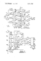
- FIG. 1 is a logic diagram showing a preferred embodiment of the invention, on the left side the phase interpolating apparatus and on the right side a phase locked clock signal generator.
- FIG. 2 is a partial logic diagram which can be utilized in conjunction with the phase interpolating apparatus of FIG. 1 for digital time interval measurement.
- Terminal 9 marked C receives a series of preferably 50% duty cycle clock pulses coming from a suitable clock generator for example at a rate of MHZ, having a period of 8 nsec.
- Gates 11 and 12 are used as buffer stages (Motorola MC 101 l I can be utilized) driving delay lines 13-16, also marked D1 to D4 respectively.
- the number and values of the delays are selected to uniformly interpolate the period of the clock, for example 0, 2, 4, 6 nsec or 2, 4, 6, 8, nsec for D1 to D4 respectively.
- the outputs of the delay lines form a multiphase, in the example a four phase, clock. These clock signals are fed into the D inputs of a multiplicity of FFs(e.g.
- MC 10231 marked 17-20, as many as the number of delay lines.
- JK FFs can also be used. Inputs and outputs are marked on FF 17 only, but all FFs are oriented the same way.
- the clock inputs of the FFs are connected to terminal 10 also marked T. At any desired T time a pulse is fed to terminal l0 and the clock inputs of the FFs. This will cause some of the FFs to trigger (set) depending on the phase relationship between the multiphase clock and the pulse at time T.
- FF 17 will be set, FFs 19 and 20 will not be, and FF 18 may be triggered marginally, that is the T pulse may come at the trailing edge of the clock pulse so, that it will take a long time for FF 18 to stabilize in either stable state.
- This phenomenon is known to those skilled in the art, and is referred to as teetering in copending application Ser. No. 427,459.
- a reclocking scheme is used: the outputs of FFs 17-20 are fed into the D inputs of FFs 22-25 together with a delayed (e.g. by 10 nsec) T pulse through D5 into the clock inputs.
- FFs 22-25 will repeat the state of FFs 17-20, except the probability of teetering will be greatly reduced with each regeneration. This reclocking can be repeated as many times as necessary. The measured probability ofteetering on the MC l023l is'once in a billion after two reclocking.
- FFs 27-30 together with delay 26 can be considered another reclocking state on FIG. 1.
- Outputs of FF's 22-25 or 27-30 therefore clearly and without ambiguity will memorize in their set pattern the relative phase between the clock and the pulse at time T. therefore the left side of FIG. 1 can be called a phase interpolator. If the relative phase between the clock and time T varies, at every 2 nsec (in the example) a new FF pattern will be memorized.
- phase interpolator can be utilized to form a phase locked clock generator.
- FFs 27-30 and delay 26 can be considered as another reclocking stage, even if designated as part of the phase locked clock generator.
- Q and 6 outputs of these FF s in pairs are fed into gates 31-34 (c,g. MC 1660) together with the multiphase clock signals at outputs of delays 13-16.
- Table I shows the principal FF patterns.
- Gate outputs 31-34 are joined to form an implied OR function. and the signal is fed through D7 delay (35) to output terminal 36. By appropriate selection of D7 the output will be a clock signal phase locked to time T within i l nsec in the example. By using a faster clock signal at C and more delay lines, FPS and gates, a phase locked clock signal with :b0.l nsec or better can be generated.
- a counting circuit can be utilized to count the phase locked clock periods. and an output pulse can be generated a selectable N count later. Without a phase locked clock there would be a full clock period uncertainty in the generated delay. with the phase locked clock shown, this uncertainty can be reduced to any desired small value.
- FIG. 2 shows how the phase interpolator can be used for time interval measurement.
- Dashed line 37 marked x--x on FIG. 2 corresponds to the same marking on FIG. 1.
- Lines 61-65 are to be connected to lines 71-75 respectively.
- Terminal C is to receive a time pulse with its length indicating the time interval to be measured
- terminal T is to be connected to the reference clock generator.
- Values of D5 and D6 should be preferably zero or the clock period.
- FF s 45-48 and 38-41 can be considered two more stages of reclocking, but these FFs have another purpose: storing the relative phase positions of the leading and trailing edges of the time pulse respectively.
- Inputs and outputs are marked on FF 38 only, but all F Fs are oriented the same way.
- Clock signal is supplied to the F Fs via gates 43, 42 and 44.
- Table II shows the possible resulting patterns. It can be seen. that at least FF 45 will be set. 0 output of 45 therefore is fed to gate 44, disabling all further clock pulses and thereby freezing the pattern in FFs 45-48. Similarly Table Ill shows all possible trailing edge patterns in FFs 38-41. At least FF 38 will be reset, therefore 45 set and 38 reset will be a necessary and sufficient condition to indicate a trailing edge. Gate 49 recognizes this AND condition and disables gate 42, thereby freezing the trailing edge patterns in FFs 38-41.
- Tables II and Ill also show how the patterns can be converted to binary code.
- Gates 50-53 are implementing this conversion.
- Binary signals A1, A2, B1, and B2 are fed into two bit full adder 54.
- Sum l and Sum 2 (55, 56) outputs are supplying the two least significant bits of the result and gate 57 is providing the carry pulse at terminal 58.
- All FFs on FIG. 2 for example could be MC 10231, all NOR gates MC 1662, Both OR gates MC 1664 and the adder MC 1059.
- the time interval measuring apparatus shown can measure short time intervals with leading and trailing edges falling in subsequent clock periods. It will be evident to those skilled in the art. that for longer time intervals the number of full clock periods should also be ,counted and than added to the interpolated leading edge plus trailing edge figures. For example if outputs of gates 49 and 43 together with 6 output of FF 45 are fed into an AND gate, the output will provide the clock pulses between leading and trailing edges and can be counted. The carry pulse, if any, at 58 should be added to this count.
- Apparatus as in claim 1 together with means connecting one of said first and second input terminal to a source of periodic clock signals.
- Apparatus as in claim 2 together with N gating means each having at least two inputs, and means connecting at least one input of each of said gating means to sources of different phases of said periodic clock signal in such manner, that output of one of said gating means will be a periodic clock signal with its phase representing the phase relationship between said first and second signals.
- Apparatus as in claim 3 together with counting means, serving to generate pulses selectably delayed from one of said first and second signals.
- Apparatus as in claim 2 together with memory means, adding means and counting means to form an interpolating time interval measuring apparatus.
- N is an integer greater than one
- step of also feeding a second signal to said first N the step of feeding the outputs of said first N flipflops to second N flip-flops
Abstract
Apparatus and method is provided by means of phase interpolation for measuring and generating time intervals with greater accuracy than that provided by the frequency of the clock utilized. A multiple phase delayed and multiple regenerated scheme is used for phase interpolation, and application of the principle for delay generation and time interval measurement is shown.
Description
United States Patent H 1 H 1 1,368 Tarczy-Hornoch Oct. 7, 1975 [54] PHASE INTERPOLATING APPARATUS AND METHQD Primary Examiner-John Kominski [76] Inventor: Zoltan Tarczy-Hornoch, 7106 Marlborough Terrace, Berkely, [57] ABSTRACT cahf' 94705 Apparatus and method is provided by means of phase [22] Filed: June 20, 1974 interpolation for measuring and generating time intervals with greater accuracy than that provided by the [21] Appl' N 48l066 frequency of the clock utilized. A multiple phase delayed and multiple regenerated scheme is used for [52] U.S. Cl. 328/155; 307/208; 307/262; phase interpolation, and application of the principle 307/293 for delay generation and time interval measurement is [51] Int. Cl. H03K 5/159 shown. [58] Field of Search 307/208, 262, 293;
9 Claims, 2 Drawing Figures U.S. Patent Oct. 7,1975 3,911,368
OUT
SUMI
sum
PHASE INTERPOLATINGAPPARATUS AND METHOD BACKGROUND OF THE INVENTION clock oscillator. Both of these clock sources are relatively complex and subject to analog drifts.
Therefore there is a need for an improved phase inlerpolating apparatus and method which is simple, fast, has high resolution, does not require periodic recalibration and can be used for both time interval measuring and delay generation.
Copending application Ser. No. 427,459 discloses a Similar principle used for pulse synchronizing.
SUMMARY OF THE INVENTION AND OBJECTS The disclosed apparatus and method uses commercially available integrated circuits to achieve subnanosecond time and phase resolution, which is with prior art methods beyond the resolution capability of said integrated circuits.
For delay generation a multiphase clock is utilized and a multiplicity of flip-flops (FF) are used to select the closest phase of the clock to an arbitrarily timed start pulse. The ambiguity of the FFs due to possible marginal triggering is eliminated by multiple reclocking. The closest phase of the clock is used as a phase locked clock for digital delay generation.
For time interval measurement a single phase clock is used in the preferred embodiment, and a time pulse, representing the time interval by its length, is delayed by a multiplicity of delay lines to generate a multiphase relationship to the clock. Again a multiplicity of FFs are used to select and memorize the closest phase relationship between the clock and the leading and trailing edges of the multiple-delayed time pulse. The full time interval is the sum of the full clock periods plus the fractional phase interpolated start and stop periods between the leading and trailing edges of thetime pulse. For elimination of FF ambiguity again reclocking is utilized.
In general, it is the object of the present invention to provide an improved phase interpolating apparatus and method.
Another object of the invention is to utilize the phase interpolating apparatus to provide an improved phase locked clock generator.
Another object of the invention is to utilize the phase locked clock generator to provide an improved digital delay generator.
Another object of the invention isto utilize the phase interpolating apparatus to provide an improved digital time interval measuring apparatus.
Another object of the invention is to provide phase interpolating. delay generating and time interval measuring apparatuses which do not require analog adjustments.
Another object of the invention is to provide phase interpolating, delay generating and time interval measuring apparatuses which can utilize commercially available integrated cicuits for high resolution and which are simple, fast and low in cost.
Additional objects and features of the invention will appear from the following description in which the preferred embodiment is set forth in conjunction with the accompanying drawings.
BRIEF DESCRIPTION OF THE DRAWINGS FIG. 1 is a logic diagram showing a preferred embodiment of the invention, on the left side the phase interpolating apparatus and on the right side a phase locked clock signal generator.
FIG. 2 is a partial logic diagram which can be utilized in conjunction with the phase interpolating apparatus of FIG. 1 for digital time interval measurement.
DESCRIPTION OF THE PREFERRED EMBODIMENT On the logic diagram of FIG. 1 elements 9-26 on the left side of dashed line 37 marked xx form a phase interpolating apparatus.
Terminal 9 marked C receives a series of preferably 50% duty cycle clock pulses coming from a suitable clock generator for example at a rate of MHZ, having a period of 8 nsec. Gates 11 and 12 are used as buffer stages (Motorola MC 101 l I can be utilized) driving delay lines 13-16, also marked D1 to D4 respectively. The number and values of the delays are selected to uniformly interpolate the period of the clock, for example 0, 2, 4, 6 nsec or 2, 4, 6, 8, nsec for D1 to D4 respectively. The outputs of the delay lines form a multiphase, in the example a four phase, clock. These clock signals are fed into the D inputs of a multiplicity of FFs(e.g. MC 10231 marked 17-20, as many as the number of delay lines. With minor changes JK FFs can also be used. Inputs and outputs are marked on FF 17 only, but all FFs are oriented the same way. The clock inputs of the FFs are connected to terminal 10 also marked T. At any desired T time a pulse is fed to terminal l0 and the clock inputs of the FFs. This will cause some of the FFs to trigger (set) depending on the phase relationship between the multiphase clock and the pulse at time T. For example FF 17 will be set, FFs 19 and 20 will not be, and FF 18 may be triggered marginally, that is the T pulse may come at the trailing edge of the clock pulse so, that it will take a long time for FF 18 to stabilize in either stable state. This phenomenon is known to those skilled in the art, and is referred to as teetering in copending application Ser. No. 427,459. To lessen the probability of this ambiguity, a reclocking scheme is used: the outputs of FFs 17-20 are fed into the D inputs of FFs 22-25 together with a delayed (e.g. by 10 nsec) T pulse through D5 into the clock inputs. FFs 22-25 will repeat the state of FFs 17-20, except the probability of teetering will be greatly reduced with each regeneration. This reclocking can be repeated as many times as necessary. The measured probability ofteetering on the MC l023l is'once in a billion after two reclocking.
FFs 27-30 together with delay 26 can be considered another reclocking state on FIG. 1. Outputs of FF's 22-25 or 27-30 therefore clearly and without ambiguity will memorize in their set pattern the relative phase between the clock and the pulse at time T. therefore the left side of FIG. 1 can be called a phase interpolator. If the relative phase between the clock and time T varies, at every 2 nsec (in the example) a new FF pattern will be memorized.
On the right side of line 37 it is shown how the phase interpolator can be utilized to form a phase locked clock generator. As said earlier, FFs 27-30 and delay 26 can be considered as another reclocking stage, even if designated as part of the phase locked clock generator. Q and 6 outputs of these FF s in pairs are fed into gates 31-34 (c,g. MC 1660) together with the multiphase clock signals at outputs of delays 13-16. Table I shows the principal FF patterns.
Table 1 Relative FF-s Phase 27 28 29 30 l l U (l l 2 I l (l O 3 l l (l 4 (l (l l l Other patterns may also appear, instead of two set FFs only one or three may be set consecutively.
It will be seen by those skilled in the art, that only one of gates 31-34 will be enabled at any one time (depending on the phase of time T) and at the output of this gate one phase of the multiphase clock will appear. Gate outputs 31-34 are joined to form an implied OR function. and the signal is fed through D7 delay (35) to output terminal 36. By appropriate selection of D7 the output will be a clock signal phase locked to time T within i l nsec in the example. By using a faster clock signal at C and more delay lines, FPS and gates, a phase locked clock signal with :b0.l nsec or better can be generated.
It will be apparent, that such a clock can be advantageously used for digital delay generation. A counting circuit can be utilized to count the phase locked clock periods. and an output pulse can be generated a selectable N count later. Without a phase locked clock there would be a full clock period uncertainty in the generated delay. with the phase locked clock shown, this uncertainty can be reduced to any desired small value.
FIG. 2 shows how the phase interpolator can be used for time interval measurement. Dashed line 37 marked x--x on FIG. 2 corresponds to the same marking on FIG. 1. Lines 61-65 are to be connected to lines 71-75 respectively. There should be a difference in the input. Terminal C is to receive a time pulse with its length indicating the time interval to be measured, terminal T is to be connected to the reference clock generator. Values of D5 and D6 should be preferably zero or the clock period. FF s 45-48 and 38-41 can be considered two more stages of reclocking, but these FFs have another purpose: storing the relative phase positions of the leading and trailing edges of the time pulse respectively. Inputs and outputs are marked on FF 38 only, but all F Fs are oriented the same way. Clock signal is supplied to the F Fs via gates 43, 42 and 44.
When the propagating leading edge of a time pulse reaches F Fs 45-48. Table II shows the possible resulting patterns. It can be seen. that at least FF 45 will be set. 0 output of 45 therefore is fed to gate 44, disabling all further clock pulses and thereby freezing the pattern in FFs 45-48. Similarly Table Ill shows all possible trailing edge patterns in FFs 38-41. At least FF 38 will be reset, therefore 45 set and 38 reset will be a necessary and sufficient condition to indicate a trailing edge. Gate 49 recognizes this AND condition and disables gate 42, thereby freezing the trailing edge patterns in FFs 38-41.
Tables II and Ill also show how the patterns can be converted to binary code. Gates 50-53 are implementing this conversion. Binary signals A1, A2, B1, and B2 are fed into two bit full adder 54. Sum l and Sum 2 (55, 56) outputs are supplying the two least significant bits of the result and gate 57 is providing the carry pulse at terminal 58. All FFs on FIG. 2 for example could be MC 10231, all NOR gates MC 1662, Both OR gates MC 1664 and the adder MC 1059.
The time interval measuring apparatus shown can measure short time intervals with leading and trailing edges falling in subsequent clock periods. It will be evident to those skilled in the art. that for longer time intervals the number of full clock periods should also be ,counted and than added to the interpolated leading edge plus trailing edge figures. For example if outputs of gates 49 and 43 together with 6 output of FF 45 are fed into an AND gate, the output will provide the clock pulses between leading and trailing edges and can be counted. The carry pulse, if any, at 58 should be added to this count.
Higher rate clocks and more than four phase interpolators together with faster FF's and gates can achieve 0.1 nsec or better time resolution.
it is apparent from the foregoing, that a new and improved phase interpolating apparatus and method also useful for delay generation and time interval measurement has been provided. Other objects and features of the invention herein before set forth also have been met.
Although the invention has been described with respect to preferred embodiments. it will be appreciated that various changes and modifications may be made therein without departing from the scope of the invention.
What is claimed is;
1. In an interpolation apparatus means connecting the input terminals of said N delay elements to a second input terminal to receive a second signal therefrom,
means connecting one output terminal each of said first N bistable circuit means to one input terminal each of said second bistable circuit means,
and means connecting another input each of said second N bistable circuit means to receive a replica of said first signal, said second N bistable circuit means thereby serving to trigger with lessened probability marginally if any of said first N bistable circuit means is marginally triggered.
2. Apparatus as in claim 1 together with means connecting one of said first and second input terminal to a source of periodic clock signals.
3. Apparatus as in claim 2 together with N gating means each having at least two inputs, and means connecting at least one input of each of said gating means to sources of different phases of said periodic clock signal in such manner, that output of one of said gating means will be a periodic clock signal with its phase representing the phase relationship between said first and second signals.
4. Apparatus as in claim 3 together with counting means, serving to generate pulses selectably delayed from one of said first and second signals.
5. Apparatus as in claim 2 together with memory means, adding means and counting means to form an interpolating time interval measuring apparatus.
6. In a method of interpolation the step of generating N signals from a first signal by delaying said first signal by N differing amounts, wherein N is an integer greater than one,
the step of feeding said N signals to first N flip-flops,
the step of also feeding a second signal to said first N the step of feeding the outputs of said first N flipflops to second N flip-flops,
and the step of also feeding a replica of said second signal to said second N flip-flops, therby causing the second N flip-flops to trigger less marginally, if any of said first N flip-flops is marginally triggered.
7. Method as in claim 6 together with the step of making one of said first and second signals periodic and the other one a reference time pulse.
8. Method as in claim 7 together with the step of seleeting by use of gating a phase of said periodic signal substantially in phase with the leading edge of said reference time pulse.
9. Method as in claim 7 together with memorizing the fractional period intervals between the edges of said time pulse and selected phase of said periodic signal, counting the number of full periods of said periodic signal during the time pulse, and summing the numbers representing said fractional perid intervals plus the
Claims (9)
1. In an interpolation apparatus at least first N and second N bistable circuit means, where N is an integer greater than one, means connecting one input each of said first N bistable circuit means to a first input terminal to receive a first signal therefrom, another input of said first N bistable circuit means connected each to an output terminal of N delay elements of differing length, wherein one delay element may represent zero delay, means connecting the input terminals of said N delay elements to a second input terminal to receive a second signal therefrom, means connecting one output terminal each of said first N bistable circuit means to one input terminal each of said second bistable circuit means, and means connecting another input each of said second N bistable circuit means to receive a replica of said first signal, said second N bistable circuit means thereby serving to trigger with lessened probability marginally if any of said first N bistable circuit means is marginally triggered.
2. Apparatus as in claim 1 together with means connecting one of said first and second input terminal to a source of periodic clock signals.
3. Apparatus as in claim 2 together with N gating means each having at least two inputs, and means connecting at least one input of each of said gating means to sources of different phases of said periodic clock signal in such manner, that output of one of said gating means will be a periodic clock signal with its phase representing the phase relationship between said first and second signals.
4. Apparatus as in claim 3 together with counting means, serving to generate pulses selectably delayed from one of said first and second signals.
5. Apparatus as in claim 2 together with memory means, adding means and counting means to form an interpolating time interval measuring apparatus.
6. In a method of interpolation the step of generating N signals from a first signal by delaying said first signal by N differing amounts, wherein N is an integer greater than one, the step of feeding said N signals to first N flip-flops, the step of also feeding a second signal to said first N flip-flops, the step of feeding the outputs of said first N flip-flops to second N flip-flops, and the step of also feeding a replica of said second signal to said second N flip-flops, therby causing the second N flip-flops to trigger less marginally, if any of said first N flip-flops is marginally triggered.
7. Method as in claim 6 together with the step of making one of said first and second signals periodic and the other one a reference time pulse.
8. Method as in claim 7 together with the step of selecting by use of gating a phase of said periodic signal substantially in phase with the leading edge of said reference time pulse.
9. Method as in claim 7 together with memorizing the fractional period intervals between the edges of said time pulse and selected phase of said periodic signal, counting the number of full periods of said periodic signal during the time pulse, and summing the numbers representing said fractional perid intervals plus the number of said full periods.
Priority Applications (1)
| Application Number | Priority Date | Filing Date | Title |
|---|---|---|---|
| US481066A US3911368A (en) | 1974-06-20 | 1974-06-20 | Phase interpolating apparatus and method |
Applications Claiming Priority (1)
| Application Number | Priority Date | Filing Date | Title |
|---|---|---|---|
| US481066A US3911368A (en) | 1974-06-20 | 1974-06-20 | Phase interpolating apparatus and method |
Publications (1)
| Publication Number | Publication Date |
|---|---|
| US3911368A true US3911368A (en) | 1975-10-07 |
Family
ID=23910444
Family Applications (1)
| Application Number | Title | Priority Date | Filing Date |
|---|---|---|---|
| US481066A Expired - Lifetime US3911368A (en) | 1974-06-20 | 1974-06-20 | Phase interpolating apparatus and method |
Country Status (1)
| Country | Link |
|---|---|
| US (1) | US3911368A (en) |
Cited By (30)
| Publication number | Priority date | Publication date | Assignee | Title |
|---|---|---|---|---|
| US4420696A (en) * | 1980-02-25 | 1983-12-13 | Hitachi, Ltd. | Pulse train producing apparatus |
| EP0183875A2 (en) * | 1983-12-29 | 1986-06-11 | Advantest Corporation | Clocked logic device |
| US4618787A (en) * | 1983-12-09 | 1986-10-21 | At&T Teletype Corporation | Adjustable time delay circuit |
| EP0208049A2 (en) * | 1985-07-10 | 1987-01-14 | Advantest Corporation | Timing generating device |
| US4782391A (en) * | 1987-08-19 | 1988-11-01 | Rca Licensing Corporation | Multiple input digital video features processor for TV signals |
| US4791488A (en) * | 1987-08-12 | 1988-12-13 | Rca Licensing Corporation | Line-locked clock signal generation system |
| DE3826717A1 (en) * | 1987-08-07 | 1989-02-16 | Rca Licensing Corp | SIGNAL PHASE COMPENSATION |
| EP0306662A2 (en) * | 1987-09-08 | 1989-03-15 | Tektronix, Inc. | Apparatus for skew compensating signals |
| US4992874A (en) * | 1989-07-03 | 1991-02-12 | Rca Licensing Corporation | Method and apparatus for correcting timing errors as for a multi-picture display |
| US5138633A (en) * | 1990-11-19 | 1992-08-11 | At&T Bell Laboratories | Method and apparatus for adaptively retiming and regenerating digital pulse signals |
| US5343082A (en) * | 1991-12-31 | 1994-08-30 | Hyundai Electronics Industries Co., Ltd. | Address transition detection circuit |
| US5534808A (en) * | 1992-01-31 | 1996-07-09 | Konica Corporation | Signal delay method, signal delay device and circuit for use in the apparatus |
| US5554945A (en) * | 1994-02-15 | 1996-09-10 | Rambus, Inc. | Voltage controlled phase shifter with unlimited range |
| US5614855A (en) * | 1994-02-15 | 1997-03-25 | Rambus, Inc. | Delay-locked loop |
| US5808498A (en) * | 1995-05-26 | 1998-09-15 | Rambus, Inc. | At frequency phase shifting circuit for use in a quadrature clock generator |
| US5864246A (en) * | 1997-03-31 | 1999-01-26 | Lsi Logic Corporation | Method and apparatus for doubling a clock signal using phase interpolation |
| US6009534A (en) * | 1998-06-01 | 1999-12-28 | Texas Instruments Incorporated | Fractional phase interpolation of ring oscillator for high resolution pre-compensation |
| US6122336A (en) * | 1997-09-11 | 2000-09-19 | Lsi Logic Corporation | Digital clock recovery circuit with phase interpolation |
| WO2001052257A1 (en) * | 2000-01-10 | 2001-07-19 | Infineon Technologies North America Corp. | Disk drive read/write channel write precompensation using phase interpolation |
| WO2001028150A3 (en) * | 1999-10-12 | 2001-09-27 | Atheros Comm Inc | Method and apparatus for eliminating the effects of frequency offsets in a digital communication system |
| US6356132B1 (en) | 2000-01-31 | 2002-03-12 | Agere Systems Guardian Corp. | Programmable delay cell |
| FR2823340A1 (en) * | 2001-04-04 | 2002-10-11 | St Microelectronics Sa | STORAGE OF AN IMMUTABLE BINARY CODE IN AN INTEGRATED CIRCUIT |
| FR2823341A1 (en) * | 2001-04-04 | 2002-10-11 | St Microelectronics Sa | IDENTIFICATION OF AN INTEGRATED CIRCUIT FROM ITS PHYSICAL MANUFACTURING PARAMETERS |
| WO2002097814A1 (en) * | 2001-05-25 | 2002-12-05 | Infineon Technologies Ag | High-speed zero phase restart of a multiphase clock |
| US6525584B2 (en) * | 2001-07-04 | 2003-02-25 | Samsung Electronics Co., Ltd. | Digital phase interpolator for controlling delay time and method thereof |
| US20030151539A1 (en) * | 2002-02-11 | 2003-08-14 | Luc Wuidart | Extraction of a binary code based on physical parameters of an integrated circuit |
| US20070290909A1 (en) * | 2006-06-19 | 2007-12-20 | Jungerman Roger L | Systems and methods for asynchronous triggering of an arbitrary waveform generator |
| US9432179B2 (en) | 2006-03-16 | 2016-08-30 | Rambus Inc. | Signaling system with adaptive timing calibration |
| US9590644B2 (en) | 2015-02-06 | 2017-03-07 | Silicon Laboratories Inc. | Managing spurs in a radio frequency circuit |
| US10461787B2 (en) | 2018-01-30 | 2019-10-29 | Silicon Laboratories Inc. | Spur mitigation for pulse output drivers in radio frequency (RF) devices |
-
1974
- 1974-06-20 US US481066A patent/US3911368A/en not_active Expired - Lifetime
Cited By (52)
| Publication number | Priority date | Publication date | Assignee | Title |
|---|---|---|---|---|
| US4420696A (en) * | 1980-02-25 | 1983-12-13 | Hitachi, Ltd. | Pulse train producing apparatus |
| US4618787A (en) * | 1983-12-09 | 1986-10-21 | At&T Teletype Corporation | Adjustable time delay circuit |
| EP0183875A2 (en) * | 1983-12-29 | 1986-06-11 | Advantest Corporation | Clocked logic device |
| EP0183875A3 (en) * | 1983-12-29 | 1987-05-27 | Takeda Riken Kogyo Kabushikikaisha | Clocked logic device |
| EP0208049A2 (en) * | 1985-07-10 | 1987-01-14 | Advantest Corporation | Timing generating device |
| EP0208049A3 (en) * | 1985-07-10 | 1988-01-20 | Advantest Corporation | Timing generating device |
| US4814879A (en) * | 1987-08-07 | 1989-03-21 | Rca Licensing Corporation | Signal phase alignment circuitry |
| DE3826717A1 (en) * | 1987-08-07 | 1989-02-16 | Rca Licensing Corp | SIGNAL PHASE COMPENSATION |
| US4791488A (en) * | 1987-08-12 | 1988-12-13 | Rca Licensing Corporation | Line-locked clock signal generation system |
| US4782391A (en) * | 1987-08-19 | 1988-11-01 | Rca Licensing Corporation | Multiple input digital video features processor for TV signals |
| EP0306662A2 (en) * | 1987-09-08 | 1989-03-15 | Tektronix, Inc. | Apparatus for skew compensating signals |
| EP0306662A3 (en) * | 1987-09-08 | 1989-08-02 | Tektronix, Inc. | Apparatus for skew compensating signals |
| US4992874A (en) * | 1989-07-03 | 1991-02-12 | Rca Licensing Corporation | Method and apparatus for correcting timing errors as for a multi-picture display |
| US5138633A (en) * | 1990-11-19 | 1992-08-11 | At&T Bell Laboratories | Method and apparatus for adaptively retiming and regenerating digital pulse signals |
| US5343082A (en) * | 1991-12-31 | 1994-08-30 | Hyundai Electronics Industries Co., Ltd. | Address transition detection circuit |
| US5686850A (en) * | 1992-01-31 | 1997-11-11 | Konica Corporation | Signal delay method, signal delay device and circuit for use in the apparatus |
| US5534808A (en) * | 1992-01-31 | 1996-07-09 | Konica Corporation | Signal delay method, signal delay device and circuit for use in the apparatus |
| US5554945A (en) * | 1994-02-15 | 1996-09-10 | Rambus, Inc. | Voltage controlled phase shifter with unlimited range |
| US5614855A (en) * | 1994-02-15 | 1997-03-25 | Rambus, Inc. | Delay-locked loop |
| USRE37452E1 (en) | 1995-05-26 | 2001-11-20 | Rambus Inc. | At frequency phase shifting circuit for use in a quadrature clock generator |
| US5808498A (en) * | 1995-05-26 | 1998-09-15 | Rambus, Inc. | At frequency phase shifting circuit for use in a quadrature clock generator |
| US5864246A (en) * | 1997-03-31 | 1999-01-26 | Lsi Logic Corporation | Method and apparatus for doubling a clock signal using phase interpolation |
| US6122336A (en) * | 1997-09-11 | 2000-09-19 | Lsi Logic Corporation | Digital clock recovery circuit with phase interpolation |
| US6009534A (en) * | 1998-06-01 | 1999-12-28 | Texas Instruments Incorporated | Fractional phase interpolation of ring oscillator for high resolution pre-compensation |
| WO2001028150A3 (en) * | 1999-10-12 | 2001-09-27 | Atheros Comm Inc | Method and apparatus for eliminating the effects of frequency offsets in a digital communication system |
| US8767893B2 (en) | 1999-10-12 | 2014-07-01 | Qualcomm Incorporated | Method and apparatus for eliminating the effects of frequency offsets in a digital communication system |
| US8363757B1 (en) | 1999-10-12 | 2013-01-29 | Qualcomm Incorporated | Method and apparatus for eliminating the effects of frequency offsets in a digital communication system |
| WO2001052257A1 (en) * | 2000-01-10 | 2001-07-19 | Infineon Technologies North America Corp. | Disk drive read/write channel write precompensation using phase interpolation |
| US6662303B1 (en) | 2000-01-10 | 2003-12-09 | Infineon Technologies North America Corp. | Write precompensation circuit and read channel with write precompensation circuit that generates output signals by interpolating between selected phases |
| US6356132B1 (en) | 2000-01-31 | 2002-03-12 | Agere Systems Guardian Corp. | Programmable delay cell |
| US7199631B2 (en) | 2001-04-04 | 2007-04-03 | Stmicroelectronics S.A. | Storing an unchanging binary code in an integrated circuit |
| US7178113B2 (en) | 2001-04-04 | 2007-02-13 | Stmicroelectronics S.A. | Identification of an integrated circuit from its physical manufacture parameters |
| WO2002082448A1 (en) * | 2001-04-04 | 2002-10-17 | Stmicroelectronics S.A. | Identification of an integrated circuit from its physical manufacture parameters |
| FR2823340A1 (en) * | 2001-04-04 | 2002-10-11 | St Microelectronics Sa | STORAGE OF AN IMMUTABLE BINARY CODE IN AN INTEGRATED CIRCUIT |
| FR2823341A1 (en) * | 2001-04-04 | 2002-10-11 | St Microelectronics Sa | IDENTIFICATION OF AN INTEGRATED CIRCUIT FROM ITS PHYSICAL MANUFACTURING PARAMETERS |
| WO2002082449A1 (en) * | 2001-04-04 | 2002-10-17 | Stmicroelectronics S.A. | Storing an unchanging binary code in an integrated circuit |
| US20040125930A1 (en) * | 2001-04-04 | 2004-07-01 | Michel Bardouillet | Identification of an integrated circuit from its physical manufacture parameters |
| US20040130363A1 (en) * | 2001-04-04 | 2004-07-08 | Michel Bardouillet | Storing an unchanging binary code in an integrated circuit |
| WO2002097814A1 (en) * | 2001-05-25 | 2002-12-05 | Infineon Technologies Ag | High-speed zero phase restart of a multiphase clock |
| US6525584B2 (en) * | 2001-07-04 | 2003-02-25 | Samsung Electronics Co., Ltd. | Digital phase interpolator for controlling delay time and method thereof |
| US6836430B2 (en) | 2002-02-11 | 2004-12-28 | Stmicroelectronics S.A. | Extraction of a binary code based on physical parameters of an integrated circuit |
| WO2003069626A1 (en) * | 2002-02-11 | 2003-08-21 | Stmicroelectronics S.A. | Extraction of a binary code from physical parameters of an integrated circuit |
| US20030151539A1 (en) * | 2002-02-11 | 2003-08-14 | Luc Wuidart | Extraction of a binary code based on physical parameters of an integrated circuit |
| US11405174B2 (en) | 2006-03-16 | 2022-08-02 | Rambus Inc. | Signaling system with adaptive timing calibration |
| US9432179B2 (en) | 2006-03-16 | 2016-08-30 | Rambus Inc. | Signaling system with adaptive timing calibration |
| US10447465B2 (en) | 2006-03-16 | 2019-10-15 | Rambus Inc. | Signaling system with adaptive timing calibration |
| US10771231B2 (en) | 2006-03-16 | 2020-09-08 | Rambus Inc. | Signaling system with adaptive timing calibration |
| US11115179B2 (en) | 2006-03-16 | 2021-09-07 | Rambus Inc. | Signaling system with adaptive timing calibration |
| US7385543B2 (en) * | 2006-06-19 | 2008-06-10 | Agilent Technologies, Inc. | Systems and methods for asynchronous triggering of an arbitrary waveform generator |
| US20070290909A1 (en) * | 2006-06-19 | 2007-12-20 | Jungerman Roger L | Systems and methods for asynchronous triggering of an arbitrary waveform generator |
| US9590644B2 (en) | 2015-02-06 | 2017-03-07 | Silicon Laboratories Inc. | Managing spurs in a radio frequency circuit |
| US10461787B2 (en) | 2018-01-30 | 2019-10-29 | Silicon Laboratories Inc. | Spur mitigation for pulse output drivers in radio frequency (RF) devices |
Similar Documents
| Publication | Publication Date | Title |
|---|---|---|
| US3911368A (en) | Phase interpolating apparatus and method | |
| CA1173917A (en) | Digital frequency divider suitable for a frequency synthesizer | |
| JPS6223495B2 (en) | ||
| US4339722A (en) | Digital frequency multiplier | |
| US3755748A (en) | Digital phase shifter/synchronizer and method of shifting | |
| US4107600A (en) | Adaptive frequency to digital converter system | |
| US3913021A (en) | High resolution digitally programmable electronic delay for multi-channel operation | |
| JPH0439690B2 (en) | ||
| US3976946A (en) | Circuit arrangement for frequency division by non-integral divisors | |
| US4754163A (en) | Pulse generator with adjustable pulse frequency, pulse width and pulse delay | |
| JPS61157022A (en) | Frequency multiplier | |
| US3840815A (en) | Programmable pulse width generator | |
| CA1216032A (en) | Variable digital frequency generator with value storage | |
| US3505594A (en) | Interpolating time interval counter with course count ambiguity eliminating means | |
| JP3397000B2 (en) | Apparatus and method for processing timing signal train | |
| US4383166A (en) | Automatic echo-chamber for measuring single time intervals by replication and averaging | |
| US3297952A (en) | Circuit arrangement for producing a pulse train in which the edges of the pulses have an exactly defined time position | |
| US3671872A (en) | High frequency multiple phase signal generator | |
| US3444462A (en) | Logic network and method for use in interpolating time interval counters | |
| RU2785070C1 (en) | Method for phase binding of the generated sequence of pulses to an external trigger pulse | |
| JP2641964B2 (en) | Divider | |
| EP0223812A1 (en) | Phase modulators | |
| SU1029403A1 (en) | Multichannel pulse generator | |
| JPH0770996B2 (en) | Method and apparatus for converting a write clock with a gear to a read clock without a gear. | |
| JPH05347555A (en) | Variable frequency divider circuit |