US20110215308A1 - Organic light-emitting device and method of manufacturing the same - Google Patents
Organic light-emitting device and method of manufacturing the same Download PDFInfo
- Publication number
- US20110215308A1 US20110215308A1 US13/042,561 US201113042561A US2011215308A1 US 20110215308 A1 US20110215308 A1 US 20110215308A1 US 201113042561 A US201113042561 A US 201113042561A US 2011215308 A1 US2011215308 A1 US 2011215308A1
- Authority
- US
- United States
- Prior art keywords
- group
- transport layer
- substituted
- unsubstituted
- hole transport
- Prior art date
- Legal status (The legal status is an assumption and is not a legal conclusion. Google has not performed a legal analysis and makes no representation as to the accuracy of the status listed.)
- Granted
Links
- 238000004519 manufacturing process Methods 0.000 title claims abstract description 9
- 239000000463 material Substances 0.000 claims abstract description 340
- 230000005525 hole transport Effects 0.000 claims abstract description 177
- 239000000758 substrate Substances 0.000 claims abstract description 32
- 230000008021 deposition Effects 0.000 claims description 95
- 229910052751 metal Inorganic materials 0.000 claims description 55
- 239000002184 metal Substances 0.000 claims description 55
- 125000004435 hydrogen atom Chemical group [H]* 0.000 claims description 37
- 125000004093 cyano group Chemical group *C#N 0.000 claims description 34
- 125000003118 aryl group Chemical group 0.000 claims description 22
- 125000001072 heteroaryl group Chemical group 0.000 claims description 22
- 150000001875 compounds Chemical class 0.000 claims description 17
- 125000005843 halogen group Chemical group 0.000 claims description 17
- 125000002887 hydroxy group Chemical group [H]O* 0.000 claims description 17
- 125000000923 (C1-C30) alkyl group Chemical group 0.000 claims description 16
- 238000000034 method Methods 0.000 claims description 16
- 125000000739 C2-C30 alkenyl group Chemical group 0.000 claims description 12
- 125000003545 alkoxy group Chemical group 0.000 claims description 12
- 125000000304 alkynyl group Chemical group 0.000 claims description 12
- 125000004414 alkyl thio group Chemical group 0.000 claims description 9
- 125000002947 alkylene group Chemical group 0.000 claims description 8
- 125000000732 arylene group Chemical group 0.000 claims description 8
- 125000005549 heteroarylene group Chemical group 0.000 claims description 8
- HUWSZNZAROKDRZ-RRLWZMAJSA-N (3r,4r)-3-azaniumyl-5-[[(2s,3r)-1-[(2s)-2,3-dicarboxypyrrolidin-1-yl]-3-methyl-1-oxopentan-2-yl]amino]-5-oxo-4-sulfanylpentane-1-sulfonate Chemical compound OS(=O)(=O)CC[C@@H](N)[C@@H](S)C(=O)N[C@@H]([C@H](C)CC)C(=O)N1CCC(C(O)=O)[C@H]1C(O)=O HUWSZNZAROKDRZ-RRLWZMAJSA-N 0.000 claims description 7
- 230000015572 biosynthetic process Effects 0.000 claims description 7
- LVDRREOUMKACNJ-BKMJKUGQSA-N N-[(2R,3S)-2-(4-chlorophenyl)-1-(1,4-dimethyl-2-oxoquinolin-7-yl)-6-oxopiperidin-3-yl]-2-methylpropane-1-sulfonamide Chemical group CC(C)CS(=O)(=O)N[C@H]1CCC(=O)N([C@@H]1c1ccc(Cl)cc1)c1ccc2c(C)cc(=O)n(C)c2c1 LVDRREOUMKACNJ-BKMJKUGQSA-N 0.000 claims description 6
- 125000004450 alkenylene group Chemical group 0.000 claims description 5
- IMKMFBIYHXBKRX-UHFFFAOYSA-M lithium;quinoline-2-carboxylate Chemical compound [Li+].C1=CC=CC2=NC(C(=O)[O-])=CC=C21 IMKMFBIYHXBKRX-UHFFFAOYSA-M 0.000 claims description 5
- 125000002252 acyl group Chemical group 0.000 claims description 4
- 125000001028 difluoromethyl group Chemical group [H]C(F)(F)* 0.000 claims description 4
- 125000004216 fluoromethyl group Chemical group [H]C([H])(F)* 0.000 claims description 4
- 125000000449 nitro group Chemical group [O-][N+](*)=O 0.000 claims description 4
- 229920006395 saturated elastomer Polymers 0.000 claims description 4
- 125000002023 trifluoromethyl group Chemical group FC(F)(F)* 0.000 claims description 4
- KKHFRAFPESRGGD-UHFFFAOYSA-N 1,3-dimethyl-7-[3-(n-methylanilino)propyl]purine-2,6-dione Chemical compound C1=NC=2N(C)C(=O)N(C)C(=O)C=2N1CCCN(C)C1=CC=CC=C1 KKHFRAFPESRGGD-UHFFFAOYSA-N 0.000 claims description 3
- MHSLDASSAFCCDO-UHFFFAOYSA-N 1-(5-tert-butyl-2-methylpyrazol-3-yl)-3-(4-pyridin-4-yloxyphenyl)urea Chemical compound CN1N=C(C(C)(C)C)C=C1NC(=O)NC(C=C1)=CC=C1OC1=CC=NC=C1 MHSLDASSAFCCDO-UHFFFAOYSA-N 0.000 claims description 2
- 239000010410 layer Substances 0.000 description 165
- 238000000151 deposition Methods 0.000 description 87
- 125000001997 phenyl group Chemical group [H]C1=C([H])C([H])=C(*)C([H])=C1[H] 0.000 description 17
- 125000001624 naphthyl group Chemical group 0.000 description 16
- -1 region Substances 0.000 description 16
- 125000005428 anthryl group Chemical group [H]C1=C([H])C([H])=C2C([H])=C3C(*)=C([H])C([H])=C([H])C3=C([H])C2=C1[H] 0.000 description 14
- 239000002356 single layer Substances 0.000 description 12
- 239000011248 coating agent Substances 0.000 description 11
- 238000000576 coating method Methods 0.000 description 11
- 238000001771 vacuum deposition Methods 0.000 description 10
- 238000002347 injection Methods 0.000 description 9
- 239000007924 injection Substances 0.000 description 9
- 239000011777 magnesium Substances 0.000 description 9
- 125000000843 phenylene group Chemical group C1(=C(C=CC=C1)*)* 0.000 description 9
- 238000004528 spin coating Methods 0.000 description 9
- 239000002019 doping agent Substances 0.000 description 8
- 125000002496 methyl group Chemical group [H]C([H])([H])* 0.000 description 8
- SZUVGFMDDVSKSI-WIFOCOSTSA-N (1s,2s,3s,5r)-1-(carboxymethyl)-3,5-bis[(4-phenoxyphenyl)methyl-propylcarbamoyl]cyclopentane-1,2-dicarboxylic acid Chemical compound O=C([C@@H]1[C@@H]([C@](CC(O)=O)([C@H](C(=O)N(CCC)CC=2C=CC(OC=3C=CC=CC=3)=CC=2)C1)C(O)=O)C(O)=O)N(CCC)CC(C=C1)=CC=C1OC1=CC=CC=C1 SZUVGFMDDVSKSI-WIFOCOSTSA-N 0.000 description 6
- 125000000008 (C1-C10) alkyl group Chemical group 0.000 description 6
- 125000000609 carbazolyl group Chemical group C1(=CC=CC=2C3=CC=CC=C3NC12)* 0.000 description 6
- 229940126543 compound 14 Drugs 0.000 description 6
- 125000001495 ethyl group Chemical group [H]C([H])([H])C([H])([H])* 0.000 description 6
- 125000003983 fluorenyl group Chemical group C1(=CC=CC=2C3=CC=CC=C3CC12)* 0.000 description 6
- 125000005566 carbazolylene group Chemical group 0.000 description 5
- 238000005755 formation reaction Methods 0.000 description 5
- 229910052749 magnesium Inorganic materials 0.000 description 5
- 238000012986 modification Methods 0.000 description 5
- 230000004048 modification Effects 0.000 description 5
- 125000004076 pyridyl group Chemical group 0.000 description 5
- 125000005551 pyridylene group Chemical group 0.000 description 5
- 125000000027 (C1-C10) alkoxy group Chemical group 0.000 description 4
- FYYHWMGAXLPEAU-UHFFFAOYSA-N Magnesium Chemical compound [Mg] FYYHWMGAXLPEAU-UHFFFAOYSA-N 0.000 description 4
- 125000004653 anthracenylene group Chemical group 0.000 description 4
- 125000000484 butyl group Chemical group [H]C([*])([H])C([H])([H])C([H])([H])C([H])([H])[H] 0.000 description 4
- 239000011575 calcium Substances 0.000 description 4
- 125000001301 ethoxy group Chemical group [H]C([H])([H])C([H])([H])O* 0.000 description 4
- 125000005567 fluorenylene group Chemical group 0.000 description 4
- 125000000956 methoxy group Chemical group [H]C([H])([H])O* 0.000 description 4
- 229920000767 polyaniline Polymers 0.000 description 4
- 125000001436 propyl group Chemical group [H]C([*])([H])C([H])([H])C([H])([H])[H] 0.000 description 4
- 125000003373 pyrazinyl group Chemical group 0.000 description 4
- 125000005558 triazinylene group Chemical group 0.000 description 4
- 125000006832 (C1-C10) alkylene group Chemical group 0.000 description 3
- VQGHOUODWALEFC-UHFFFAOYSA-N 2-phenylpyridine Chemical compound C1=CC=CC=C1C1=CC=CC=N1 VQGHOUODWALEFC-UHFFFAOYSA-N 0.000 description 3
- KFZMGEQAYNKOFK-UHFFFAOYSA-N Isopropanol Chemical compound CC(C)O KFZMGEQAYNKOFK-UHFFFAOYSA-N 0.000 description 3
- 229910052782 aluminium Inorganic materials 0.000 description 3
- XAGFODPZIPBFFR-UHFFFAOYSA-N aluminium Chemical compound [Al] XAGFODPZIPBFFR-UHFFFAOYSA-N 0.000 description 3
- 230000008901 benefit Effects 0.000 description 3
- 238000005266 casting Methods 0.000 description 3
- 125000004957 naphthylene group Chemical group 0.000 description 3
- 230000008569 process Effects 0.000 description 3
- TVIVIEFSHFOWTE-UHFFFAOYSA-K tri(quinolin-8-yloxy)alumane Chemical compound [Al+3].C1=CN=C2C([O-])=CC=CC2=C1.C1=CN=C2C([O-])=CC=CC2=C1.C1=CN=C2C([O-])=CC=CC2=C1 TVIVIEFSHFOWTE-UHFFFAOYSA-K 0.000 description 3
- UHXOHPVVEHBKKT-UHFFFAOYSA-N 1-(2,2-diphenylethenyl)-4-[4-(2,2-diphenylethenyl)phenyl]benzene Chemical group C=1C=C(C=2C=CC(C=C(C=3C=CC=CC=3)C=3C=CC=CC=3)=CC=2)C=CC=1C=C(C=1C=CC=CC=1)C1=CC=CC=C1 UHXOHPVVEHBKKT-UHFFFAOYSA-N 0.000 description 2
- GEQBRULPNIVQPP-UHFFFAOYSA-N 2-[3,5-bis(1-phenylbenzimidazol-2-yl)phenyl]-1-phenylbenzimidazole Chemical compound C1=CC=CC=C1N1C2=CC=CC=C2N=C1C1=CC(C=2N(C3=CC=CC=C3N=2)C=2C=CC=CC=2)=CC(C=2N(C3=CC=CC=C3N=2)C=2C=CC=CC=2)=C1 GEQBRULPNIVQPP-UHFFFAOYSA-N 0.000 description 2
- OBAJPWYDYFEBTF-UHFFFAOYSA-N 2-tert-butyl-9,10-dinaphthalen-2-ylanthracene Chemical compound C1=CC=CC2=CC(C3=C4C=CC=CC4=C(C=4C=C5C=CC=CC5=CC=4)C4=CC=C(C=C43)C(C)(C)C)=CC=C21 OBAJPWYDYFEBTF-UHFFFAOYSA-N 0.000 description 2
- VFUDMQLBKNMONU-UHFFFAOYSA-N 9-[4-(4-carbazol-9-ylphenyl)phenyl]carbazole Chemical group C12=CC=CC=C2C2=CC=CC=C2N1C1=CC=C(C=2C=CC(=CC=2)N2C3=CC=CC=C3C3=CC=CC=C32)C=C1 VFUDMQLBKNMONU-UHFFFAOYSA-N 0.000 description 2
- OYPRJOBELJOOCE-UHFFFAOYSA-N Calcium Chemical compound [Ca] OYPRJOBELJOOCE-UHFFFAOYSA-N 0.000 description 2
- 229920001609 Poly(3,4-ethylenedioxythiophene) Polymers 0.000 description 2
- FAPWRFPIFSIZLT-UHFFFAOYSA-M Sodium chloride Chemical compound [Na+].[Cl-] FAPWRFPIFSIZLT-UHFFFAOYSA-M 0.000 description 2
- 230000000903 blocking effect Effects 0.000 description 2
- 125000004106 butoxy group Chemical group [*]OC([H])([H])C([H])([H])C(C([H])([H])[H])([H])[H] 0.000 description 2
- 229910052791 calcium Inorganic materials 0.000 description 2
- 239000000969 carrier Substances 0.000 description 2
- 230000008859 change Effects 0.000 description 2
- 239000004020 conductor Substances 0.000 description 2
- 239000011521 glass Substances 0.000 description 2
- 125000002883 imidazolyl group Chemical group 0.000 description 2
- 229910052744 lithium Inorganic materials 0.000 description 2
- 230000005012 migration Effects 0.000 description 2
- 238000013508 migration Methods 0.000 description 2
- 125000001147 pentyl group Chemical group C(CCCC)* 0.000 description 2
- 229920003227 poly(N-vinyl carbazole) Polymers 0.000 description 2
- 125000002572 propoxy group Chemical group [*]OC([H])([H])C(C([H])([H])[H])([H])[H] 0.000 description 2
- 125000005550 pyrazinylene group Chemical group 0.000 description 2
- 125000001725 pyrenyl group Chemical group 0.000 description 2
- 125000002943 quinolinyl group Chemical group N1=C(C=CC2=CC=CC=C12)* 0.000 description 2
- 229910052709 silver Inorganic materials 0.000 description 2
- 125000001424 substituent group Chemical group 0.000 description 2
- XOLBLPGZBRYERU-UHFFFAOYSA-N tin dioxide Chemical compound O=[Sn]=O XOLBLPGZBRYERU-UHFFFAOYSA-N 0.000 description 2
- VIJSPAIQWVPKQZ-BLECARSGSA-N (2s)-2-[[(2s)-2-[[(2s)-2-[[(2s)-2-[[(2s)-2-[[(2s)-2-acetamido-5-(diaminomethylideneamino)pentanoyl]amino]-4-methylpentanoyl]amino]-4,4-dimethylpentanoyl]amino]-4-methylpentanoyl]amino]propanoyl]amino]-5-(diaminomethylideneamino)pentanoic acid Chemical compound NC(=N)NCCC[C@@H](C(O)=O)NC(=O)[C@H](C)NC(=O)[C@H](CC(C)C)NC(=O)[C@H](CC(C)(C)C)NC(=O)[C@H](CC(C)C)NC(=O)[C@H](CCCNC(N)=N)NC(C)=O VIJSPAIQWVPKQZ-BLECARSGSA-N 0.000 description 1
- MIOPJNTWMNEORI-GMSGAONNSA-N (S)-camphorsulfonic acid Chemical compound C1C[C@@]2(CS(O)(=O)=O)C(=O)C[C@@H]1C2(C)C MIOPJNTWMNEORI-GMSGAONNSA-N 0.000 description 1
- IWZZBBJTIUYDPZ-DVACKJPTSA-N (z)-4-hydroxypent-3-en-2-one;iridium;2-phenylpyridine Chemical compound [Ir].C\C(O)=C\C(C)=O.[C-]1=CC=CC=C1C1=CC=CC=N1.[C-]1=CC=CC=C1C1=CC=CC=N1 IWZZBBJTIUYDPZ-DVACKJPTSA-N 0.000 description 1
- IYZMXHQDXZKNCY-UHFFFAOYSA-N 1-n,1-n-diphenyl-4-n,4-n-bis[4-(n-phenylanilino)phenyl]benzene-1,4-diamine Chemical compound C1=CC=CC=C1N(C=1C=CC(=CC=1)N(C=1C=CC(=CC=1)N(C=1C=CC=CC=1)C=1C=CC=CC=1)C=1C=CC(=CC=1)N(C=1C=CC=CC=1)C=1C=CC=CC=1)C1=CC=CC=C1 IYZMXHQDXZKNCY-UHFFFAOYSA-N 0.000 description 1
- BFTIPCRZWILUIY-UHFFFAOYSA-N 2,5,8,11-tetratert-butylperylene Chemical group CC(C)(C)C1=CC(C2=CC(C(C)(C)C)=CC=3C2=C2C=C(C=3)C(C)(C)C)=C3C2=CC(C(C)(C)C)=CC3=C1 BFTIPCRZWILUIY-UHFFFAOYSA-N 0.000 description 1
- XANIFASCQKHXRC-UHFFFAOYSA-N 2-(1,3-benzothiazol-2-yl)phenol zinc Chemical compound [Zn].Oc1ccccc1-c1nc2ccccc2s1.Oc1ccccc1-c1nc2ccccc2s1 XANIFASCQKHXRC-UHFFFAOYSA-N 0.000 description 1
- ATKYPLNPUMJYCQ-UHFFFAOYSA-N 2-(2-hydroxyphenyl)-3H-1,3-benzothiazole-2-carboxylic acid Chemical compound N1C2=CC=CC=C2SC1(C(=O)O)C1=CC=CC=C1O ATKYPLNPUMJYCQ-UHFFFAOYSA-N 0.000 description 1
- LFOIDLOIBZFWDO-UHFFFAOYSA-N 2-methoxy-6-[6-methoxy-4-[(3-phenylmethoxyphenyl)methoxy]-1-benzofuran-2-yl]imidazo[2,1-b][1,3,4]thiadiazole Chemical compound N1=C2SC(OC)=NN2C=C1C(OC1=CC(OC)=C2)=CC1=C2OCC(C=1)=CC=CC=1OCC1=CC=CC=C1 LFOIDLOIBZFWDO-UHFFFAOYSA-N 0.000 description 1
- NSMJMUQZRGZMQC-UHFFFAOYSA-N 2-naphthalen-1-yl-1H-imidazo[4,5-f][1,10]phenanthroline Chemical compound C12=CC=CN=C2C2=NC=CC=C2C2=C1NC(C=1C3=CC=CC=C3C=CC=1)=N2 NSMJMUQZRGZMQC-UHFFFAOYSA-N 0.000 description 1
- AWXGSYPUMWKTBR-UHFFFAOYSA-N 4-carbazol-9-yl-n,n-bis(4-carbazol-9-ylphenyl)aniline Chemical compound C12=CC=CC=C2C2=CC=CC=C2N1C1=CC=C(N(C=2C=CC(=CC=2)N2C3=CC=CC=C3C3=CC=CC=C32)C=2C=CC(=CC=2)N2C3=CC=CC=C3C3=CC=CC=C32)C=C1 AWXGSYPUMWKTBR-UHFFFAOYSA-N 0.000 description 1
- MAGFQRLKWCCTQJ-UHFFFAOYSA-M 4-ethenylbenzenesulfonate Chemical compound [O-]S(=O)(=O)C1=CC=C(C=C)C=C1 MAGFQRLKWCCTQJ-UHFFFAOYSA-M 0.000 description 1
- OSQXTXTYKAEHQV-WXUKJITCSA-N 4-methyl-n-[4-[(e)-2-[4-[4-[(e)-2-[4-(4-methyl-n-(4-methylphenyl)anilino)phenyl]ethenyl]phenyl]phenyl]ethenyl]phenyl]-n-(4-methylphenyl)aniline Chemical compound C1=CC(C)=CC=C1N(C=1C=CC(\C=C\C=2C=CC(=CC=2)C=2C=CC(\C=C\C=3C=CC(=CC=3)N(C=3C=CC(C)=CC=3)C=3C=CC(C)=CC=3)=CC=2)=CC=1)C1=CC=C(C)C=C1 OSQXTXTYKAEHQV-WXUKJITCSA-N 0.000 description 1
- DIVZFUBWFAOMCW-UHFFFAOYSA-N 4-n-(3-methylphenyl)-1-n,1-n-bis[4-(n-(3-methylphenyl)anilino)phenyl]-4-n-phenylbenzene-1,4-diamine Chemical compound CC1=CC=CC(N(C=2C=CC=CC=2)C=2C=CC(=CC=2)N(C=2C=CC(=CC=2)N(C=2C=CC=CC=2)C=2C=C(C)C=CC=2)C=2C=CC(=CC=2)N(C=2C=CC=CC=2)C=2C=C(C)C=CC=2)=C1 DIVZFUBWFAOMCW-UHFFFAOYSA-N 0.000 description 1
- VIZUPBYFLORCRA-UHFFFAOYSA-N 9,10-dinaphthalen-2-ylanthracene Chemical compound C12=CC=CC=C2C(C2=CC3=CC=CC=C3C=C2)=C(C=CC=C2)C2=C1C1=CC=C(C=CC=C2)C2=C1 VIZUPBYFLORCRA-UHFFFAOYSA-N 0.000 description 1
- 229910001148 Al-Li alloy Inorganic materials 0.000 description 1
- KAKZBPTYRLMSJV-UHFFFAOYSA-N Butadiene Chemical group C=CC=C KAKZBPTYRLMSJV-UHFFFAOYSA-N 0.000 description 1
- 125000006374 C2-C10 alkenyl group Chemical group 0.000 description 1
- 125000005865 C2-C10alkynyl group Chemical group 0.000 description 1
- 101000837344 Homo sapiens T-cell leukemia translocation-altered gene protein Proteins 0.000 description 1
- UFHFLCQGNIYNRP-UHFFFAOYSA-N Hydrogen Chemical compound [H][H] UFHFLCQGNIYNRP-UHFFFAOYSA-N 0.000 description 1
- FUJCRWPEOMXPAD-UHFFFAOYSA-N Li2O Inorganic materials [Li+].[Li+].[O-2] FUJCRWPEOMXPAD-UHFFFAOYSA-N 0.000 description 1
- WHXSMMKQMYFTQS-UHFFFAOYSA-N Lithium Chemical compound [Li] WHXSMMKQMYFTQS-UHFFFAOYSA-N 0.000 description 1
- 102100028692 T-cell leukemia translocation-altered gene protein Human genes 0.000 description 1
- HCHKCACWOHOZIP-UHFFFAOYSA-N Zinc Chemical compound [Zn] HCHKCACWOHOZIP-UHFFFAOYSA-N 0.000 description 1
- JHYLKGDXMUDNEO-UHFFFAOYSA-N [Mg].[In] Chemical compound [Mg].[In] JHYLKGDXMUDNEO-UHFFFAOYSA-N 0.000 description 1
- 125000004054 acenaphthylenyl group Chemical group C1(=CC2=CC=CC3=CC=CC1=C23)* 0.000 description 1
- CUJRVFIICFDLGR-UHFFFAOYSA-N acetylacetonate Chemical compound CC(=O)[CH-]C(C)=O CUJRVFIICFDLGR-UHFFFAOYSA-N 0.000 description 1
- 229910045601 alloy Inorganic materials 0.000 description 1
- 239000000956 alloy Substances 0.000 description 1
- QVQLCTNNEUAWMS-UHFFFAOYSA-N barium oxide Inorganic materials [Ba]=O QVQLCTNNEUAWMS-UHFFFAOYSA-N 0.000 description 1
- LPTWEDZIPSKWDG-UHFFFAOYSA-N benzenesulfonic acid;dodecane Chemical compound OS(=O)(=O)C1=CC=CC=C1.CCCCCCCCCCCC LPTWEDZIPSKWDG-UHFFFAOYSA-N 0.000 description 1
- XJHCXCQVJFPJIK-UHFFFAOYSA-M caesium fluoride Inorganic materials [F-].[Cs+] XJHCXCQVJFPJIK-UHFFFAOYSA-M 0.000 description 1
- 239000002800 charge carrier Substances 0.000 description 1
- 125000005584 chrysenylene group Chemical group 0.000 description 1
- 229940126545 compound 53 Drugs 0.000 description 1
- 125000004802 cyanophenyl group Chemical group 0.000 description 1
- 238000009792 diffusion process Methods 0.000 description 1
- XUCJHNOBJLKZNU-UHFFFAOYSA-M dilithium;hydroxide Chemical compound [Li+].[Li+].[OH-] XUCJHNOBJLKZNU-UHFFFAOYSA-M 0.000 description 1
- 229940060296 dodecylbenzenesulfonic acid Drugs 0.000 description 1
- 125000000816 ethylene group Chemical group [H]C([H])([*:1])C([H])([H])[*:2] 0.000 description 1
- 238000011156 evaluation Methods 0.000 description 1
- 230000005281 excited state Effects 0.000 description 1
- 239000010408 film Substances 0.000 description 1
- 125000001153 fluoro group Chemical group F* 0.000 description 1
- JVZRCNQLWOELDU-UHFFFAOYSA-N gamma-Phenylpyridine Natural products C1=CC=CC=C1C1=CC=NC=C1 JVZRCNQLWOELDU-UHFFFAOYSA-N 0.000 description 1
- 230000005283 ground state Effects 0.000 description 1
- 238000010438 heat treatment Methods 0.000 description 1
- RBTKNAXYKSUFRK-UHFFFAOYSA-N heliogen blue Chemical compound [Cu].[N-]1C2=C(C=CC=C3)C3=C1N=C([N-]1)C3=CC=CC=C3C1=NC([N-]1)=C(C=CC=C3)C3=C1N=C([N-]1)C3=CC=CC=C3C1=N2 RBTKNAXYKSUFRK-UHFFFAOYSA-N 0.000 description 1
- 229910052739 hydrogen Inorganic materials 0.000 description 1
- 239000001257 hydrogen Substances 0.000 description 1
- 125000002636 imidazolinyl group Chemical group 0.000 description 1
- 229910052738 indium Inorganic materials 0.000 description 1
- CECAIMUJVYQLKA-UHFFFAOYSA-N iridium 1-phenylisoquinoline Chemical compound [Ir].C1=CC=CC=C1C1=NC=CC2=CC=CC=C12.C1=CC=CC=C1C1=NC=CC2=CC=CC=C12.C1=CC=CC=C1C1=NC=CC2=CC=CC=C12 CECAIMUJVYQLKA-UHFFFAOYSA-N 0.000 description 1
- PQXKHYXIUOZZFA-UHFFFAOYSA-M lithium fluoride Inorganic materials [Li+].[F-] PQXKHYXIUOZZFA-UHFFFAOYSA-M 0.000 description 1
- SJCKRGFTWFGHGZ-UHFFFAOYSA-N magnesium silver Chemical compound [Mg].[Ag] SJCKRGFTWFGHGZ-UHFFFAOYSA-N 0.000 description 1
- 238000005259 measurement Methods 0.000 description 1
- 239000000203 mixture Substances 0.000 description 1
- YPJRZWDWVBNDIW-UHFFFAOYSA-N n,n-diphenyl-4-[2-[4-[4-[2-[4-(n-phenylanilino)phenyl]ethenyl]phenyl]phenyl]ethenyl]aniline Chemical group C=1C=C(N(C=2C=CC=CC=2)C=2C=CC=CC=2)C=CC=1C=CC(C=C1)=CC=C1C(C=C1)=CC=C1C=CC(C=C1)=CC=C1N(C=1C=CC=CC=1)C1=CC=CC=C1 YPJRZWDWVBNDIW-UHFFFAOYSA-N 0.000 description 1
- IBHBKWKFFTZAHE-UHFFFAOYSA-N n-[4-[4-(n-naphthalen-1-ylanilino)phenyl]phenyl]-n-phenylnaphthalen-1-amine Chemical compound C1=CC=CC=C1N(C=1C2=CC=CC=C2C=CC=1)C1=CC=C(C=2C=CC(=CC=2)N(C=2C=CC=CC=2)C=2C3=CC=CC=C3C=CC=2)C=C1 IBHBKWKFFTZAHE-UHFFFAOYSA-N 0.000 description 1
- 150000002894 organic compounds Chemical class 0.000 description 1
- 150000004866 oxadiazoles Chemical class 0.000 description 1
- MHAUGLFOVCQYNR-UHFFFAOYSA-N pentaphenylene Chemical group C1=CC=C2C3=CC=CC=C3C3=CC=CC=C3C3=CC=CC=C3C3=CC=CC=C3C2=C1 MHAUGLFOVCQYNR-UHFFFAOYSA-N 0.000 description 1
- 125000005563 perylenylene group Chemical group 0.000 description 1
- 125000005560 phenanthrenylene group Chemical group 0.000 description 1
- 229920003023 plastic Polymers 0.000 description 1
- 125000005548 pyrenylene group Chemical group 0.000 description 1
- 125000005576 pyrimidinylene group Chemical group 0.000 description 1
- FDBYIYFVSAHJLY-UHFFFAOYSA-N resmetirom Chemical compound N1C(=O)C(C(C)C)=CC(OC=2C(=CC(=CC=2Cl)N2C(NC(=O)C(C#N)=N2)=O)Cl)=N1 FDBYIYFVSAHJLY-UHFFFAOYSA-N 0.000 description 1
- 230000004044 response Effects 0.000 description 1
- 238000007789 sealing Methods 0.000 description 1
- 239000004332 silver Substances 0.000 description 1
- 239000011780 sodium chloride Substances 0.000 description 1
- 239000002904 solvent Substances 0.000 description 1
- 238000004544 sputter deposition Methods 0.000 description 1
- 239000000126 substance Substances 0.000 description 1
- 125000005760 substituted naphthylene group Chemical group 0.000 description 1
- 125000005650 substituted phenylene group Chemical group 0.000 description 1
- 239000010409 thin film Substances 0.000 description 1
- 125000005730 thiophenylene group Chemical group 0.000 description 1
- 239000012780 transparent material Substances 0.000 description 1
- 150000003852 triazoles Chemical class 0.000 description 1
- XLYOFNOQVPJJNP-UHFFFAOYSA-N water Substances O XLYOFNOQVPJJNP-UHFFFAOYSA-N 0.000 description 1
- 229910052725 zinc Inorganic materials 0.000 description 1
- 239000011701 zinc Substances 0.000 description 1
Images


Classifications
-
- H—ELECTRICITY
- H10—SEMICONDUCTOR DEVICES; ELECTRIC SOLID-STATE DEVICES NOT OTHERWISE PROVIDED FOR
- H10K—ORGANIC ELECTRIC SOLID-STATE DEVICES
- H10K50/00—Organic light-emitting devices
- H10K50/10—OLEDs or polymer light-emitting diodes [PLED]
- H10K50/14—Carrier transporting layers
- H10K50/15—Hole transporting layers
- H10K50/156—Hole transporting layers comprising a multilayered structure
-
- H—ELECTRICITY
- H10—SEMICONDUCTOR DEVICES; ELECTRIC SOLID-STATE DEVICES NOT OTHERWISE PROVIDED FOR
- H10K—ORGANIC ELECTRIC SOLID-STATE DEVICES
- H10K85/00—Organic materials used in the body or electrodes of devices covered by this subclass
- H10K85/60—Organic compounds having low molecular weight
- H10K85/631—Amine compounds having at least two aryl rest on at least one amine-nitrogen atom, e.g. triphenylamine
- H10K85/633—Amine compounds having at least two aryl rest on at least one amine-nitrogen atom, e.g. triphenylamine comprising polycyclic condensed aromatic hydrocarbons as substituents on the nitrogen atom
-
- H—ELECTRICITY
- H10—SEMICONDUCTOR DEVICES; ELECTRIC SOLID-STATE DEVICES NOT OTHERWISE PROVIDED FOR
- H10K—ORGANIC ELECTRIC SOLID-STATE DEVICES
- H10K85/00—Organic materials used in the body or electrodes of devices covered by this subclass
- H10K85/60—Organic compounds having low molecular weight
- H10K85/631—Amine compounds having at least two aryl rest on at least one amine-nitrogen atom, e.g. triphenylamine
- H10K85/636—Amine compounds having at least two aryl rest on at least one amine-nitrogen atom, e.g. triphenylamine comprising heteroaromatic hydrocarbons as substituents on the nitrogen atom
-
- H—ELECTRICITY
- H10—SEMICONDUCTOR DEVICES; ELECTRIC SOLID-STATE DEVICES NOT OTHERWISE PROVIDED FOR
- H10K—ORGANIC ELECTRIC SOLID-STATE DEVICES
- H10K85/00—Organic materials used in the body or electrodes of devices covered by this subclass
- H10K85/60—Organic compounds having low molecular weight
- H10K85/649—Aromatic compounds comprising a hetero atom
- H10K85/657—Polycyclic condensed heteroaromatic hydrocarbons
- H10K85/6572—Polycyclic condensed heteroaromatic hydrocarbons comprising only nitrogen in the heteroaromatic polycondensed ring system, e.g. phenanthroline or carbazole
-
- H—ELECTRICITY
- H10—SEMICONDUCTOR DEVICES; ELECTRIC SOLID-STATE DEVICES NOT OTHERWISE PROVIDED FOR
- H10K—ORGANIC ELECTRIC SOLID-STATE DEVICES
- H10K50/00—Organic light-emitting devices
- H10K50/10—OLEDs or polymer light-emitting diodes [PLED]
- H10K50/14—Carrier transporting layers
-
- H—ELECTRICITY
- H10—SEMICONDUCTOR DEVICES; ELECTRIC SOLID-STATE DEVICES NOT OTHERWISE PROVIDED FOR
- H10K—ORGANIC ELECTRIC SOLID-STATE DEVICES
- H10K85/00—Organic materials used in the body or electrodes of devices covered by this subclass
- H10K85/10—Organic polymers or oligomers
- H10K85/111—Organic polymers or oligomers comprising aromatic, heteroaromatic, or aryl chains, e.g. polyaniline, polyphenylene or polyphenylene vinylene
- H10K85/115—Polyfluorene; Derivatives thereof
-
- H—ELECTRICITY
- H10—SEMICONDUCTOR DEVICES; ELECTRIC SOLID-STATE DEVICES NOT OTHERWISE PROVIDED FOR
- H10K—ORGANIC ELECTRIC SOLID-STATE DEVICES
- H10K85/00—Organic materials used in the body or electrodes of devices covered by this subclass
- H10K85/30—Coordination compounds
-
- H—ELECTRICITY
- H10—SEMICONDUCTOR DEVICES; ELECTRIC SOLID-STATE DEVICES NOT OTHERWISE PROVIDED FOR
- H10K—ORGANIC ELECTRIC SOLID-STATE DEVICES
- H10K85/00—Organic materials used in the body or electrodes of devices covered by this subclass
- H10K85/30—Coordination compounds
- H10K85/341—Transition metal complexes, e.g. Ru(II)polypyridine complexes
- H10K85/344—Transition metal complexes, e.g. Ru(II)polypyridine complexes comprising ruthenium
-
- H—ELECTRICITY
- H10—SEMICONDUCTOR DEVICES; ELECTRIC SOLID-STATE DEVICES NOT OTHERWISE PROVIDED FOR
- H10K—ORGANIC ELECTRIC SOLID-STATE DEVICES
- H10K85/00—Organic materials used in the body or electrodes of devices covered by this subclass
- H10K85/30—Coordination compounds
- H10K85/341—Transition metal complexes, e.g. Ru(II)polypyridine complexes
- H10K85/346—Transition metal complexes, e.g. Ru(II)polypyridine complexes comprising platinum
-
- H—ELECTRICITY
- H10—SEMICONDUCTOR DEVICES; ELECTRIC SOLID-STATE DEVICES NOT OTHERWISE PROVIDED FOR
- H10K—ORGANIC ELECTRIC SOLID-STATE DEVICES
- H10K85/00—Organic materials used in the body or electrodes of devices covered by this subclass
- H10K85/60—Organic compounds having low molecular weight
- H10K85/615—Polycyclic condensed aromatic hydrocarbons, e.g. anthracene
- H10K85/626—Polycyclic condensed aromatic hydrocarbons, e.g. anthracene containing more than one polycyclic condensed aromatic rings, e.g. bis-anthracene
Definitions
- One or more embodiments of the present invention relate to an organic light-emitting device and a method of manufacturing the same.
- OLEDs which are self-emitting devices, have advantages such as a wide viewing angle, excellent contrast, quick response, high brightness, excellent driving voltage characteristics, and can provide multicolored images.
- a typical OLED has a structure including a substrate, and an anode, a hole transport layer (HTL), an emission layer (EML), an electron transport layer (ETL), and a cathode which are sequentially stacked on the substrate.
- HTL hole transport layer
- EML emission layer
- ETL electron transport layer
- cathode cathode
- the HTL, the EML, and the ETL are organic thin films formed of organic compounds.
- An operating principle of an OLED having the above-described structure is as follows.
- One or more embodiments of the present invention include an organic light-emitting device (OLED).
- OLED organic light-emitting device
- One or more embodiments of the present invention include a method of manufacturing the OLED.
- an organic light-emitting device includes: a substrate; a first electrode; a second electrode; and a hole transport layer, an emission layer, and an electron transport layer between the first electrode and the second electrode,
- the hole transport layer includes at least one hole transport unit including: a first hole transport layer including a hole transporting material; a third hole transport layer formed on the first hole transport layer and including a charge generating material; and a fifth hole transport layer formed on the third hole transport layer and including the hole transporting material, and
- the electron transport layer includes an electron transporting material and a metal-containing material.
- the hole transport unit may further include at least one layer selected from the group consisting of a second hole transport layer interposed between the first hole transport layer and the third hole transport layer and including the hole transporting material and the charge generating material, and a fourth hole transport layer interposed between the third hole transport layer and the fifth hole transport layer and including the hole transporting material and the charge generating material.
- the hole transporting material may be represented by one selected from the group consisting of Formulae 1 and 2 below:
- R 10 is represented by —(Ar 1 ) n —Ar 2 ;
- R 16 is represented by —(Ar 11 ) m —Ar 12 ;
- Ar 1 , Ar 11 , L 1 , and L 11 are each independently selected from the group consisting of a substituted or unsubstituted C 1 -C 30 alkylene group, a substituted or unsubstituted C 2 -C 30 alkenylene group, a substituted or unsubstituted C 5 -C 30 arylene group, a substituted or unsubstituted C 4 -C 30 heteroarylene group, and —N(Q 1 )-;
- n, m, a, and b are each independently an integer from 0 to 10;
- R 1 through R 3 , R 11 through R 15 , R 17 , R 18 , R 21 through R 29 , Ar 2 , Ar 12 , and Q 1 are each independently selected from the group consisting of a hydrogen
- C 1 -C 30 alkyl group a substituted or unsubstituted C 2 -C 30 alkenyl group, a substituted or unsubstituted C 2 -C 30 alkynyl group, a substituted or unsubstituted C 1 -C 30 alkoxy group, a substituted or unsubstituted C 1 -C 30 alkylthiol group, a substituted or unsubstituted C 5 -C 30 aryl group, and a substituted or unsubstituted C 4 -C 30 heteroaryl group, wherein n groups of Ar 1 in —(Ar 1 ) n — may be identical to or different from each other, m groups of Ar 11 in —(Ar 11 ) m — may be identical to or different from each other, a groups of L 1 in -(L 1 ) a - may be identical to or different from each other, and b groups of L 11 in -(L 11 ) b
- the charge generating material may include a compound represented by Formula 3 below:
- R 51 to R 56 are each independently selected from the group consisting of a hydrogen atom, —CN, —SOR 100 , —SON(R 101 ) 2 , —SO 2 R 102 , —SO 2 N(R 103 ) 2 , —SO 3 R 104 , —SO 3 N(R 105 ) 2 , —NO 2 , —CFH 2 , —CF 2 H, and —CF 3
- R 100 to R 105 are each independently selected from the group consisting of a hydrogen atom, a substituted or unsubstituted C 1 -C 30 alkyl group, a substituted or unsubstituted C 5 -C 30 aryl group, and a substituted or unsubstituted C 4 -C 30 heteroaryl group.
- the thicknesses of the first hole transport layer, the third hole transport layer, and the fifth hole transport layer may be each independently in the range of about 0.1 nm to about 100 nm.
- the thicknesses of the second hole transport layer and the fourth hole transport layer may be each independently in the range of about 0.01 nm to about 16 nm.
- the amount of the charge generating material contained in the second hole transport layer may be in the range of about 0.01 to about 99 parts by weight based on 100 parts by weight of the second hole transport layer, and the amount of the charge generating material contained in the fourth hole transport layer may be in the range of about 0.01 to about 99 parts by weight based on 100 parts by weight of the fourth hole transport layer.
- the third hole transport layer may include two charge generating material-containing layers, and the interface between the two charge generating material-containing layers is not clearly distinguished, so that the third hole transport layer is seen as a single layer.
- the hole transport layer may include two hole transport units.
- the electron transporting material contained in the electron transport layer may be selected from the group consisting of Compound 60 and compounds represented by Formulae 4 and 5 below:
- R 61 to R 66 are each independently a hydrogen atom, a halogen atom, a hydroxy group, a cyano group, a substituted or unsubstituted.
- L 21 is a substituted or unsubstituted C 1 -C 30 alkylene group, a substituted or unsubstituted C 6 -C 30 arylene group, or a substituted or unsubstituted C 3 -C 30 heteroarylene group;
- Q 11 through Q 19 are each independently a hydrogen atom, a substituted or unsubstituted C 6 -C 30 aryl group, or a substituted or unsubstituted C 3 -C 30 heteroaryl group;
- c is an integer from 0 to 10.
- the metal-containing material contained in the electron transport layer may include a Li complex.
- the electron transport layer may include at least one electron transport unit including: a first electron transport layer including the electron transporting material; a third electron transport layer formed on the first electron transport layer and including the metal-containing material; and a fifth electron transport layer formed on the third electron transport layer and including the electron transporting material.
- the electron transport unit may further include at least one layer selected from the group consisting of a second electron transport layer interposed between the first electron transport layer and the third electron transport layer and including the electron transporting material and the metal-containing material, and a fourth electron transport layer interposed between the third electron transport layer and the fifth electron transport layer and including the electron transporting material and the metal-containing material.
- the third electron transport layer may include two metal-containing material-containing layers, and the interface between the two metal-containing material-containing layers is not clearly distinguished, so that the third electron transport layer is seen as a single layer.
- the electron transport layer may include two electron transport units.
- a method of manufacturing an organic light-emitting device includes:
- an electron transport layer including an electron transporting material and a metal-containing material on the emission layer
- the forming the hole transport layer includes:
- a hole transport layer including at least one hole transport unit including: a first hole transport layer including the hole transporting material; a third hole transport layer formed on the first hole transport layer and including the charge generating material; and a fifth hole transport layer formed on the third hole transport layer and including the hole transporting material, by performing at least one reciprocation of the first deposition source and the second deposition source from a first end to a second end, and then the second end to the first end of a region in which the hole transport layer is formed, or
- first deposition source and the second deposition source disposing the first deposition source and the second deposition source to be spaced apart from each other such that a region to which the hole transporting material is released overlaps a region to which the charge generating material is released;
- a hole transport layer including at least one hole transport unit including: a first hole transport layer including the hole transporting material; a third hole transport layer formed on the first hole transport layer and including the charge generating material; and a fifth hole transport layer formed on the third hole transport layer and including the hole transporting material, and at least one layer selected from the group consisting of a second hole transport layer interposed between the first hole transport layer and the third hole transport layer and including the hole transporting material and the charge generating material, and a fourth hole transport layer interposed between the third hole transport layer and the fifth hole transport layer and including the hole transporting material and the charge generating material, by performing at least one reciprocation of the first deposition source and the second deposition source from a first end to a second end, and then the second end to the first end of a region in which the hole transport layer is formed.
- FIG. 1 is a schematic cross-sectional view of an organic light-emitting device (OLED) according to an embodiment of the present invention
- FIG. 2 is a schematic cross-sectional view of an OLED according to another embodiment of the present invention.
- FIG. 3 is a schematic cross-sectional view of an OLED according to another embodiment of the present invention.
- FIG. 4 is a schematic cross-sectional view of an OLED according to another embodiment of the present invention.
- FIGS. 5A to 5G schematically illustrate a method of forming a hole transport layer of the OLED of FIG. 1 , according to an embodiment of the present invention
- FIG. 6 is a schematic cross-sectional view of an OLED according to another embodiment of the present invention.
- FIG. 7 is a graph illustrating time-brightness of an OLED according to Example 1.
- FIG. 8 is a graph illustrating voltage-current density of an OLED according to Example 1.
- the expression “An A layer is formed on a B layer (or the surface of a B layer)” is used to describe a structure in which the A layer is formed to cover at least a part of the B layer (or the surface of the B layer). It will be understood when the expression of “An A layer is formed on a B layer (or the surface of a B layer)” is used, or when an element such as a layer, film, region, or substrate is referred to as being “on” another element, the layer or the element can be formed directly on the another element, or one or more intervening elements may also be present. The structure would have been obvious to those of ordinary skill in the art. In the specification and the claim section, when a chemical formula of (X) n or a similar formula is used, it will be understood that n groups of X in the formula (X) n may be identical to or different from each other unless otherwise stated.
- FIG. 1 is a schematic sectional view of an organic light-emitting device (OLED) 100 according to an embodiment of the present invention.
- the OLED 100 includes a substrate 110 , and a first electrode 120 , a hole injection layer (HIL) 130 , a hole transport layer (HTL) 140 , an emission layer (EML) 150 , an electron transport layer (ETL) 160 , an electron injection layer (EIL) 180 , and a second electrode 190 which are sequentially stacked on the substrate 110 in the stated order.
- HIL hole injection layer
- HTL hole transport layer
- EML emission layer
- ETL electron transport layer
- EIL electron injection layer
- the HTL 140 includes one hole transport unit including: a first HTL 141 having a hole transporting material; a second HTL 142 formed on the first HTL 141 and having the hole transporting material and a charge generating material; a third HTL 143 formed on the second HTL 142 and having the charge generating material; a fourth HTL 144 formed on the third HTL 143 and having the hole transporting material and the charge generating material; and a fifth HTL 145 formed on the fourth HTL 144 and having the hole transporting material.
- the substrate 110 which may be any substrate that is generally used in organic light-emitting devices, may be a glass substrate or a transparent plastic substrate with excellent mechanical strength, thermal stability, transparency, surface smoothness, ease of handling, and waterproofness.
- the first electrode 120 is formed on the substrate 110 .
- the first electrode 120 may be formed by depositing or sputtering a material used to form the first electrode 120 on the substrate 110 .
- the first electrode 120 may be an anode.
- the material used to form the first electrode 120 may be a high work-function material so as to facilitate hole injection.
- the first electrode 120 may be a transmissive electrode or a semi-transmissive electrode. Transparent and conductive materials such as ITO, IZO, SnO 2 , and ZnO may be used to form the first electrode 120 .
- the first electrode 120 may be formed as a semi-transmissive electrode using magnesium (Mg), aluminum (Al), aluminum-lithium (Al—Li), calcium (Ca), magnesium-indium (Mg—In), magnesium-silver (Mg—Ag), or the like.
- Mg magnesium
- Al aluminum
- Al—Li aluminum-lithium
- Ca calcium
- Mg—In magnesium-indium
- Mg—Ag magnesium-silver
- the HIL 130 may be disposed on the first electrode 120 .
- the HIL 130 may be formed on the first electrode 120 by vacuum deposition, spin coating, casting, LB deposition, or the like.
- the deposition conditions may vary according to a compound that is used to form the HIL 130 , and the structure and thermal properties of the HIL 130 to be formed.
- conditions for vacuum deposition may include a deposition temperature of about 100 to about 500° C., a pressure of about 10 ⁇ 8 to about 10 ⁇ 3 torr, and a deposition rate of about 0.01 to about 100 ⁇ /sec.
- the coating conditions may vary according to a compound that is used to form the HIL 130 , and the structure and thermal properties of the HIL 130 to be formed. In general, however, the coating rate may be in the range of about 2000 to about 5000 rpm, and a temperature for heat treatment which is performed to remove a solvent after coating may be in the range of about 80 to about 200° C.
- the HIL 130 may be formed of any material that is commonly used to form a HIL.
- the material that may be used to form the HIL 130 include, but are not limited to, a phthalocyanine compound such as copperphthalocyanine, 4,4′,4′′-tris (3-methylphenylphenylamino)triphenyl amine (m-MTDATA), N,N′-di(1-naphthyl)-N,N′-diphenylbenzidine (NPB), TDATA, 2T-NATA, polyaniline/dodecylbenzenesulfonic acid (Pani/DBS A), poly(3,4-ethylenedioxythiophene)/poly(4-styrenesulfonate) (PEDOT/PSS), polyaniline/camphor sulfonicacid (Pani/CSA), and polyaniline)/poly(4-styrenesulfonate (PANI/PSS).
- a phthalocyanine compound
- the thickness of the HIL 130 may be in the range of about 100 to about 10,000 ⁇ , for example, about 100 to about 1000 ⁇ . When the thickness of the HIL 130 is within this range of about 100 to about 10,000 ⁇ , the HIL 130 may have excellent hole injecting ability without a substantial increase in driving voltage.
- the HTL 140 is disposed on the HIL 130 .
- the HTL 140 includes the hole transport unit including: the first HTL 141 having a hole transporting material; the second HTL 142 formed on the first HTL 141 and having the hole transporting material and a charge generating material; the third HTL 143 formed on the second HTL 142 and having the charge generating material; the fourth HTL 144 formed on the third HTL 143 and having the hole transporting material and the charge generating material; and the fifth HTL 145 formed on the fourth HTL 144 and having the hole transporting material.
- the HTL 140 has a structure in which the second HTL 142 , the third HTL 143 , the fourth HTL 144 , and the fifth HTL 145 are sequentially stacked on the first HTL 141 in the order stated, so that injection and transport of holes may be controlled and electrons may be blocked.
- the number of excitons generated in emission regions may be gradually reduced since the amount of electrons or holes may change with time during the operation of the OLED 100 . As a result, a carrier balance may not be maintained, and thus, the lifetime of the OLED 100 may be reduced.
- the HTL 140 has a stack structure of a plurality of layers with a similar or same energy level (the first HTL 141 , the second HTL 142 , the third HTL 143 , the fourth HTL 144 , and the fifth HTL 145 ), the flow of carriers may be constantly maintained while controlling migration rates of holes. Thus, lifetime characteristics of the OLED 100 may be improved.
- the hole transporting material may be represented by one selected from the group consisting of Formulae 1 and 2 below.
- R 10 is represented by —(Ar 1 ) n —Ar 2 ;
- R 16 is represented by —(Ar 11 ) m —Ar 12 ;
- Ar 1 , Ar 11 , L 1 , and L 11 are each independently selected from the group consisting of a substituted or unsubstituted C 1 -C 30 alkylene group, a substituted or unsubstituted C 2 -C 30 alkenylene group, a substituted or unsubstituted C 5 -C 30 arylene group, a substituted or unsubstituted C 4 -C 30 heteroarylene group, and —N(Q 1 )-;
- n, m, a, and b are each independently an integer from 0 to 10;
- R 1 through R 3 , R 11 through R 15 , R 17 , R 18 , R 21 through R 29 , Ar 2 , Ar 12 , and Q 1 are each independently selected from the group consisting of a hydrogen
- Ar 1 in the formula —(Ar 1 ) n —Ar 2 — for R 10 and Ar 11 in the formula —(Ar 11 ) m —Ar 12 — for R 16 include a substituted or unsubstituted C 1 -C 10 alkylene group, a substituted or unsubstituted C 2 -C 10 alkenylene group, a substituted or unsubstituted phenylene group, a substituted or unsubstituted pentalenylene group, a substituted or unsubstituted indenylene group, a substituted or unsubstituted naphthylene group, a substituted or unsubstituted azulenylene group, a substituted or unsubstituted heptalenylene group, a substituted or unsubstituted indacenylene group, a substituted or unsubstituted acenaphthylene group, a substituted or
- Q 1 may be selected from the group consisting of a hydrogen atom, a halogen atom, a hydroxyl group, a cyano group, a substituted or unsubstituted C 1 -C 10 alkyl group, a substituted or unsubstituted C 2 -C 10 alkenyl group, a substituted or unsubstituted C 2 -C 10 alkynyl group, a substituted or unsubstituted C 1 -C 10 alkoxy group, a substituted or unsubstituted C 1 -C 10 alkylthiol group, a substituted or unsubstituted C 5 -C 14 aryl group, a substituted or unsubstituted C 4 -C 14 heteroaryl group, and —N(Q 2 )(Q 3 ), but is not limited thereto.
- Ar 1 and Ar 11 may be each independently selected from the group consisting of a C 1 -C 10 alkylene group; a phenylene group; a naphthylene group; an anthrylene group; a fluorenylene group; a carbazolylene group; a pyrazolylene group; a pyridinylene group; a triazinylene group; —N(Q 1 )-; and a substituted C 1 -C 10 alkylene group, a substituted phenylene group, a substituted naphthylene group, a substituted anthrylene group, a substituted fluorenylene group, a substituted carbazolylene group, a substituted pyrazolylene group, a substituted pyridinylene group, and a substituted triazinylene group which have at least one substituent selected from the group consisting of a halogen atom, a cyano group, a hydroxyl group, a C 1 -
- Q 1 may be selected from the group consisting of a hydrogen atom; a C 1 -C 10 alkyl group; a phenyl group; a naphthyl group; a carbazolyl group; a fluorenyl group; a pyrenyl group; a substituted C 1 -C 10 alkyl group, a substituted C 1 -C 10 alkoxy group, a substituted phenyl group, a substituted naphthyl group, a substituted carbazolyl group, a to substituted fluorenyl group, and a substituted pyrenyl group which have at least one substituent selected from the group consisting of a halogen atom, a cyano group, a hydroxyl group, a C 1 -C 10 alkyl group, a C 1 -C 10 alkoxy group, a phenyl group, a naphthyl group, and an anthryl group; and —N(Q 2 atom,
- Ar 2 in the formula —(Ar 1 ) n —Ar 2 — and Ar 12 in the formula —(Ar 11 ) m —Ar 12 - are as defined above in connection with Q 1 .
- n in the formula —(Ar 1 ) n —Ar 2 — and m in the formula —(Ar 11 ) m —Ar 12 — are each independently an integer from 0 to 10.
- n and m may be each independently 0, 1, 2, 3, 4, or 5, but are not limited thereto.
- n groups of Ar 1 in the formula —(Ar 1 ) n —Ar 2 — may be identical to or different from each other.
- the two groups of Ar 1 in —(Ar 1 ) n — may be both phenylene groups, or one of the two may be —N(Q 1 )- and the other may be a phenylene group, and various modifications may be applied thereto.
- the descriptions of —(Ar 11 ) m —Ar 12 — may be the same as those of —(Ar 1 ) n —Ar 2 — above.
- R 1 through R 3 , R 11 through R 15 , R 17 , R 18 , and R 21 through R 29 in Formulae 1 and 2 may be defined as described above in connection with Q 1 .
- R 13 may be a phenyl group, a naphthyl group, or an anthryl group, but is not limited thereto.
- R 28 and R 29 may be each independently selected from the group consisting of a hydrogen atom, a methyl group, an ethyl group, a methoxy group, an ethoxy group, a phenyl group, a naphthyl group, and an anthryl group, but are not limited thereto.
- L 1 and L 2 in Formulae 1 and 2 are defined as described above in connection with Ar 1 and Ar 11 .
- L 1 and L 2 may be each independently a phenylene group, a carbazolylene group, or a phenylcarbazolylene group, but are not limited thereto.
- a and b may be each independently an integer from 0 to 10.
- a and b may be each independently 0, 1, 2 or 3, but are not limited thereto.
- Ar 1 in the formula —(Ar 1 ) n —Ar 2 — for R 10 and Ar 11 in the formula —(Ar 11 ) m —Ar 12 — for R 16 may be each independently selected from the group consisting of a phenylene group; a carbazolylene group; a fluorenylene group; a methylfluorenylene group; a pyrazolylene group; a phenylpyrazolylene group; —N(Q 1 )-, wherein Q 1 is a hydrogen atom, a phenyl group, a fluorenyl group, a dimethylfluorenyl group, a diphenylfluorenyl group, a carbazolyl group, or a phenylcarbazolyl group; a diphenylfluorenylene group; a triazinylene group; a methyltriazinylene group; a phenyltriazinylene group;
- R 11 , R 12 , R 14 , R 15 , R 17 , R 18 , and R 21 through R 27 may be hydrogen;
- R 13 may be selected from the group consisting of a phenyl group, a naphthyl group, and an anthryl group;
- R 28 and R 29 may be each independently selected from the group consisting of a hydrogen atom, a methyl group, an ethyl group, a methoxy group, an ethoxy group, a phenyl group, a naphthyl group, and an anthryl group;
- L 11 may be a phenylene group; and
- b may be 0 or 1.
- the hole transporting material may be any one of the Compounds 1 through 37 below, but is not limited thereto.
- the charge generating material is material generating charge carriers (i.e., holes and/or electrons) upon exposure to light.
- the charge generating material may include a compound represented by Formula 3 below.
- R 51 to R 56 are each independently selected from the group consisting of a hydrogen atom, —CN, —SOR 100 , —SON(R 101 ) 2, —SO 2 R 102 , —SO 2 N(R 103 ) 2 , —SO 3 R 104 , —SO 3 N(R 105 ) 2 , —NO 2 , —CFH 2 , —CF 2 H, and —CF 3
- R 100 to R 105 are each independently selected from the group consisting of a hydrogen atom, a substituted or unsubstituted C 1 -C 30 alkyl group, a substituted or unsubstituted C 5 -C 30 aryl group, and a substituted or unsubstituted C 4 -C 30 heteroaryl group.
- R 100 through R 105 may be each independently selected from the group consisting of a hydrogen atom, a substituted or unsubstituted C 1 -C 10 alkyl group, a substituted or unsubstituted C 5 -C 14 aryl group, and a substituted or unsubstituted C 4 -C 14 heteroaryl group.
- R 100 to R 105 may be each independently selected from the group consisting of a hydrogen atom, a methyl group, an ethyl group, a propyl group, a butyl group, a pentyl group, a methyl group substituted with at least one —CN group, an ethyl group substituted with at least one —CN group, a propyl group substituted with at least one —CN, a butyl group substituted with at least one —CN, a pentyl group substituted with at least one —CN, a phenyl group, a naphthyl group, an anthryl group, a fluorenyl group, a phenyl group substituted with at least one —CN, a naphthyl group substituted with at least one —CN, an anthryl group substituted with at least one —CN, a fluorenyl group substituted with at least one —CN, a carbazolyl group, a
- the charge generating material may be Compound 40 below, but is not limited thereto.
- the thicknesses of the first HTL 141 , the third HTL 143 , and the fifth HTL 145 may be each independently in the range of about 0.1 nm to about 100 nm.
- the thicknesses of the first HTL 141 and the fifth HTL 145 may be each independently in the range of about 10 nm to about 100 nm, for example, about 50 mn to about 60 nm, but are not limited thereto.
- the thickness of the third HTL 143 may be in the range of about 0.5 nm to about 100 nm, for example, about 0.5 nm to about 10 nm, but is not limited thereto.
- the thicknesses of the first HTL 141 , the third HTL 143 , and the fifth HTL 145 are within this range of about 0.1 nm to about 100 nm, holes may be effectively injected and transported to the EML 150 without a substantial increase in driving voltage.
- the thicknesses of the first HTL 141 , the third HTL 143 , and the fifth HTL 145 may be the same or different.
- the thicknesses of the second HTL 142 and the fourth HTL 144 may be each independently in the range of about 0.01 nm to about 16 nm, for example, about 0.5 nm to about 1 nm. When the thicknesses of the second HTL 142 and the fourth HTL 144 are within this range of about 0.01 nm to about 16 nm, holes may be effectively injected and transported to the EML 150 without a substantial increase in driving voltage.
- the thicknesses of the second HTL 142 and the fourth HTL 144 may be the same or different.
- the amount of the charge generating material contained in the second HTL 142 may be in the range of about 0.01 to about 99 parts by weight, for example, about 45 to about 55 parts by weight based on 100 parts by weight of the second HTL 142 .
- the amount of the charge generating material contained in the fourth. HTL 144 may be in the range of about 0.01 to about 99 parts by weight, for example, about 45 to about 55 parts by weight based on 100 parts by weight of the fourth HTL 144 .
- the efficiency of OLED 100 may be improved.
- the HTL 140 may be formed by using vacuum deposition, spin coating, casting, or the like.
- the deposition and coating conditions may be similar to those for the formation of the HIL 130 , though the deposition and coating conditions may vary according to the material that is used to form the HTL 140 .
- the HTL 140 may be formed by preparing a first deposition source releasing the hole transporting material and a second deposition source releasing the charge generating material, disposing the first deposition source and the second deposition source to be spaced apart from each other such that a region to which the hole transporting material is released overlaps a region to which the charge generating material is released, and performing one reciprocation of the first and second deposition sources from a first end to a second end, and then from the second end to the first end of a region on which the HTL 140 will be formed on the HIL 130 in FIG. 1 .
- FIGS. 5A to 5G schematically illustrate a method of forming a HTL 140 on the HIL 130 , according to an embodiment of the present invention.
- the substrate 110 and the first electrode 120 are disposed at one surface of the HIL 130 on which the HTL 140 is not formed, they are not shown in FIGS. 5A to 5G for descriptive convenience.
- a first deposition source 1001 and a second deposition source 1002 may be disposed below one surface of the HIL 130 , i.e., the surface on which the substrate 110 and the first electrode 120 are not formed.
- the first deposition source 1001 may be a deposition source releasing the hole transporting material
- the second deposition source 1002 may be a deposition source releasing the charge generating material.
- a region C 1 to which the hole transporting material is released by the first deposition source 1001 and a region C 2 to which the charge generating material is released by the second deposition source 1002 may have a fan shape with a predetermined angle.
- the first deposition source 1001 and the second deposition source 1002 are disposed to be spaced apart from each other such that the region C 1 to which the hole transporting material is released overlaps the region C 2 to which the charge generating material is released. Accordingly, the hole transporting material and the charge generating material may be simultaneously deposited to form the second HTL 142 and the fourth HTL 144 including both of the hole transporting material and the charge generating material as shown in FIGS. 5B and 5F .
- the first deposition source 1001 and the second deposition source 1002 may be mounted on a base 1006 that is disposed on a guide rail 1005 that is disposed in a chamber and reciprocates along the guide rail 1005 .
- the base 1006 may be connected to a separate drive unit (not shown) to operate.
- the base 1006 on which the first deposition source 1001 and the second deposition source 1002 are mounted to be spaced apart from each other by a predetermined distance may move in the B direction from a first end A below the HIL 130 when the first deposition source 1001 and the second deposition source 1002 are in an “on” state as shown in FIG. 5A .
- only the hole transporting material is deposited on the HIL 130 to form the first HTL 141 including the hole transporting material (D 1 ).
- the first HTL 141 is continuously deposited toward a second end E below the HIL 130 as the base 1006 moves in the B direction.
- a region (D 2 ) on which the hole transporting material and the charge generating material are simultaneously deposited is formed to form the second HTL 142 , including the hole transporting material and the charge generating material, on the first HTL 141 as shown in FIG. 5B .
- the second HTL 142 is continuously deposited toward the second end E with respect to the second end E (See FIG. 5D ) as the base 1006 moves in the B direction.
- a first charge generating material-containing layer 143 ′ (D 3 ) is formed on the second HTL 142 as shown in FIG. 5C .
- the first HTL 141 including the hole transporting material, the second HTL 142 including the hole transporting material and the charge generating material, and the first charge generating material-containing layer 143 ′ are formed on the HIL 130 as shown in FIG. 5D .
- a second charge generating material-containing layer 143 ′′ is first formed as shown in FIG. 5E .
- the fourth HTL 144 including the hole transporting material and the charge generating material and the fifth HTL 145 including the hole transporting material are sequentially formed on the second charge generating material-containing layer 143 ′′ as shown in FIG. 5F .
- the first charge generating material-containing layer 143 ′ and the second charge generating material-containing layer 143 ′′ have the same component, i.e., the charge generating material
- the interface between the first charge generating material-containing layer 143 ′ and the second charge generating material-containing layer 143 ′′ may not be clearly distinguished, so that they may be seen as a single layer, i.e., the third HTL 143 including the charge generating material.
- the interface between the first charge generating material-containing layer 143 ′ and the second charge generating material-containing layer 143 ′′ is shown as a dash line instead of a solid line in FIG. 5F .
- the first HTL 141 including the hole transporting material, the second HTL 142 including the hole transporting material and the charge generating material, the third HTL 143 including the charge generating material, the fourth HTL 144 including the hole transporting material and the charge generating material, and the fifth HTL 145 including the hole transporting material may be sequentially formed on the HIL 130 as shown in FIG. 5G .
- the third HTL 143 includes two charge generating material-containing layers, i.e., the first charge generating material-containing layer 143 ′ and the second charge generating material-containing layer 143 ′′
- an interface S′ between the first charge generating material-containing layer 143 ′ and the second charge generating material-containing layer 143 ′′ is not clearly distinguished, so that they may be seen as a single layer.
- the interface S′ is shown as a dash line in FIG. 5G
- the HTL 140 including one hole transport unit having the first HTL 141 , the second HTL 142 , the third HTL 143 , the fourth HTL 144 , and the fifth HTL 145 may be prepared by one reciprocation of the base 1006 on which the first deposition source 1001 and the second deposition source 1002 are mounted from the first end A to the second end E, and then from the second end E to the first end A.
- one hole transport unit may be formed using the method of forming the layers shown in FIG. 5A to 5G .
- the stacking process is simply and quickly performed, and a plurality of layers may be simultaneously deposited in a single chamber without evacuating the chamber between the formations of the layers.
- the EML 150 may be formed on the HTL 140 by vacuum deposition, spin coating, casting, LB deposition, or the like.
- the conditions for deposition and coating are similar to those for the formation of the HIL 130 , although the conditions for deposition and coating may vary according to the material that is used to form the EML 150 .
- the EML 150 may be formed of a compound, or a combination of a host and a dopant.
- the host include, but are not limited to, Alq 3 , 4,4′-N,N′- dicarbazole-biphenyl (CBP), poly(n-vinylcarbazole) (PVK), 9,10-di(naphthalene-2-yl)anthracene (ADN), TCTA, 1,3.5-tris(N-phenylbenzimidazole-2-yl)benzene (TPBI), 3-tert-butyl-9,10-di-2-naphthyl anthracene (TBADN), E3, distyrylarylene (DSA), bis(2-(2-hydroxyphenyl)benzothiazolate)zinc (Zn(BTZ) 2 ), Compound 51 below, and Compound 52 below.
- CBP 4,4′-N,N′- dicarbazole-biphenyl
- PVK poly
- red dopants examples include PtOEP, Ir(piq) 3 , and Btp 2 Ir(acac), but are not limited thereto.
- examples of known blue dopants include F 2 Irpic, (F 2 ppy) 2 Ir(tmd), Ir(dfppz) 3 , ter-fluorene, 4,4′-bis(4-diphenyl aminostyryl)biphenyl (DPAVBi), 2,5,8,11-tetra-tert-butyl perylene (TBPe), Compound 54 below, and 4,4′-bis(2,2-diphenylethenyl)biphenyl (DPVBi).
- the amount of the dopant may be in the range of about 0.01 to about 15 parts by weight based on 100 parts by weight of the host, but is not limited thereto.
- the thickness of the EML 150 may be in the range of about 100 to about 1,000 ⁇ , for example, about 200 to about 600 ⁇ . When the thickness of the EML 150 is within this range of about 100 to about 1,000 ⁇ , the EML 150 may have excellent light emitting ability without a substantial increase in driving voltage.
- a hole blocking layer (not shown in FIG. 1 ) may be formed on the EML 150 by using vacuum deposition, spin coating, casting, LB deposition, or the like, in order to prevent diffusion of triplet excitons or holes into an ETL 160 .
- the HBL is formed using vacuum deposition or spin coating, the conditions for deposition and coating may be similar to those for the formation of the HIL 130 , although the conditions for deposition and coating may vary according to the material that is used to form the HBL. Any material that is commonly used to form a HBL may be used. Examples of materials for forming the HBL include an oxadiazole derivative, a triazole derivative, and a phenanthroline derivative, but are not limited thereto.
- the thickness of the HBL may be in a range of about 50 to about 1,000 ⁇ , for example, about 100 to about 300 ⁇ . When the thickness of the HBL is within this range of about 50 to about 1,000 ⁇ , the HBL may have excellent hole blocking ability without a substantial increase in driving voltage.
- the ETL 160 is formed on the EML 150 or on the HBL if the HBL is formed.
- the ETL 160 includes an electron transporting material and a metal-containing material.
- the electron transporting material may be any electron transporting material.
- the electron transporting material may be selected from the group consisting of Compound 60 and compounds represented by Formulae 4, and 5 below.
- R 61 to R 66 are each independently a hydrogen atom, a halogen atom, a hydroxy group, a cyano group, a substituted or unsubstituted C 1 -C 30 alkyl group, a substituted or unsubstituted C 1 -C 30 alkoxy group, a substituted or unsubstituted C 1 -C 30 acyl group, a substituted or unsubstituted C 2 -C 30 alkenyl group, a substituted or unsubstituted C 2 -C 30 alkynyl group, a substituted or unsubstituted C 6 -C 30 aryl group, or a substituted or unsubstituted C 3 -C 30 heteroaryl group, wherein at least two adjacent groups of R 61 to R 66 are optionally bonded to each other to form a saturated or unsaturated ring;
- L 21 is a substituted or unsubstituted C 1 -C 30 alkylene group, a substituted or unsubstituted C 6 -C 30 arylene group, or a substituted or unsubstituted C 3 -C 30 heteroarylene group;
- Q 11 through Q 19 are, each independently, a hydrogen atom, a substituted or unsubstituted C 6 -C 30 aryl group, or a substituted or unsubstituted C 3 -C 30 heteroaryl group;
- c is an integer from 0 to 10.
- R 61 to R 66 may be each independently selected from the group consisting of a hydrogen atom, a halogen atom, a hydroxyl group, a cyano group, a methyl group, an ethyl group, a propyl group, a butyl group, a methoxy group, an ethoxy group, a propoxy group, a butoxy group, a phenyl group, a naphthyl group, an anthryl group, a pyridinyl group, and a pyrazinyl group, but are not limited thereto.
- R 61 to R 64 may be hydrogen atoms
- R 65 may be selected from the group consisting of a halogen atom, a hydroxyl group, a cyano group, a methyl group, an ethyl group, a propyl group, a butyl group, a methoxy group, an ethoxy group, a propoxy group, a butoxy group, a phenyl group, a naphthyl group, an anthryl group, a pyridinyl group, and a pyrazinyl group.
- R 61 to R 66 may be hydrogen atoms, but are not limited thereto.
- Q 11 and Q 19 may be each independently selected from the group consisting of a hydrogen atom, a phenyl group, a naphthyl group, an anthryl group, a pyridinyl group, and a pyrazinyl group, but are not limited thereto.
- Q 11 , Q 13 through Q 16 , Q 18 , and Q 19 may be hydrogen atoms
- Q 12 and Q 17 may be each independently selected from the group consisting of a phenyl group, a naphthyl group, an anthryl group, a pyridinyl group, and a pyrazinyl group, but are not limited thereto.
- L 21 may be selected from the group consisting of a phenylene group, a naphthylene group, an anthrylene group, a pyridinylene group, and a pyrazinylene group, but is not limited thereto.
- L 21 may be a phenylene group or a pyridinylene group.
- c may be 1, 2, or 3, but is not limited thereto.
- the electron transport material may be Compound 60 shown above or Compound 61 or 62 below.
- the metal-containing material may inject electrons and block holes.
- the metal-containing material may be a Li complex.
- the metal-containing material may be lithium quinolate (LiQ) or Compound 81 below, but is not limited thereto.
- the thickness of the ETL 160 may be in the range of about 50 to about 1,000 ⁇ , for example, about 100 to about 300 ⁇ . When the thickness of the ETL 160 is within the range of about 50 to about 1,000 ⁇ , an excellent electron transporting ability of the ETL 160 may be obtained without a substantial increase in driving voltage.
- the EIL 180 which facilitates injection of electrons from the cathode (second electrode 190 ), may be formed on the ETL 160 .
- Examples of materials for forming the EIL 180 include LiF, NaCl, CsF, Li 2 O, and BaO, which are known in the art.
- Deposition and coating conditions for forming the EIL 180 are similar to those for the formation of the HIL 130 , although the deposition and coating conditions may vary according to a material that is used to form the EIL 180 .
- the thickness of the EIL 180 may be in the range of about 1 to about 100 ⁇ , for example, about 5 to about 90 ⁇ . When the thickness of the EIL 180 is within this range of about 1 to about 100 ⁇ , the EIL 180 may have satisfactory electron injecting ability without a substantial increase in driving voltage.
- the second electrode 190 is disposed on the EIL 180 .
- the second electrode 190 may be a cathode, which is an electron injecting electrode.
- a metal for forming the second electrode 190 may be a metal, an alloy, an electrically conductive compound, which have a low-work function, or a mixture thereof.
- the second electrode 190 may be a reflective electrode formed of lithium (Li), magnesium (Mg), aluminum (Al), aluminum (Al)-lithium (Li), calcium (Ca), magnesium (Mg)-indium (In), magnesium (Mg)-silver (Ag), or the like.
- the second electrode 190 may be a transmissive or semi-transmissive electrode formed of a transparent conductive material such as ITO and IZO.
- the HTL 140 of the OLED 100 has a multi-layered structure, in which energy levels of the layers are similar to each other, and the ETL 160 includes the electron transporting material and the metal-containing material.
- the balance in the flow of holes and electrons is maintained for a long period of time, the injection and transport of electrons are adjusted, and holes are blocked, so that the OLED 100 may have long lifetime.
- FIG. 2 is a schematic cross-sectional view of an OLED 200 according to another embodiment of the present invention.
- the OLED 200 includes a substrate 210 , and a first electrode 220 , a HIL 230 , a HTL 240 , an EML 250 , an ETL 260 , an EIL 280 , and a second electrode 290 which are sequentially stacked on the substrate 210 in the order stated.
- the HTL 240 include two hole transport units, i.e., a first hole transport unit 240 a and a second hole transport unit 240 b .
- the HTL 240 includes: the first hole transport unit 240 a including a first HTL 241 having a hole transporting material; a second HTL 242 formed on the first HTL 241 and having the hole transporting material and a charge generating material; a third HTL 243 formed on the second HTL 242 and having the charge generating material; a fourth HTL 244 formed on the third HTL 243 and having the hole transporting material and the charge generating material; and a fifth HTL 245 formed on the fourth HTL 244 and having the hole transporting material; and the second hole transport unit 240 b including a sixth HTL 246 formed on the fifth HTL 245 and having the hole transporting material; a seventh HTL 247 formed on the sixth HTL 246 and having the hole transporting material and the charge generating material; an eighth HTL 248 formed on the seventh H
- the method of forming the layers described with reference to FIGS. 5A to 5G may be repeated twice to prepare the HTL 240 .
- the base 1006 on which the first deposition source 1001 and the second deposition source 1002 are mounted is reciprocated twice along the guide rail 1005 .
- the HTL 240 may be formed by the following process: start from the first end A ⁇ move in the B direction ⁇ arrive at the second end E ⁇ move in the F direction ⁇ arrive at the first end A ⁇ move in the B direction ⁇ arrive at the second end E ⁇ move in the F direction ⁇ arrive at the first end A.
- the third HTL 243 includes two charge generating material-containing layers, i.e., a first charge generating material-containing layer 243 ′ and a second charge generating material-containing layer 243 ′′, and components of the two layers are the same as the charge generating material.
- the interface between the first charge generating material-containing layer 243 ′ and the second charge generating material-containing layer 243 ′′ is not clearly distinguished, so that the third HTL 243 may be seen as a single layer.
- the eighth HTL 248 includes two charge generating material-containing layers, i.e., a first charge generating material-containing layer 248 ′ and a second charge generating material-containing layer 248 ′′, and components of the two layers are the same as the charge generating material.
- the interface between the first charge generating material-containing layer 248 ′ and the second charge generating material-containing layer 248 ′′ is not clearly distinguished, so that the eighth HTL 248 may be seen as a single layer.
- the interface between the first charge generating material-containing layer 243 ′ and the second charge generating material-containing layer 243 ′′ of the third HTL 243 and the interface between the first charge generating material-containing layer 248 ′ and the second charge generating material-containing layer 248 ′′ of the eighth HTL 248 are shown as a dash line instead of a solid line in FIG. 2 .
- the interface between the fifth HTL 245 and the sixth HTL 246 is shown as a dash line in FIG. 2 . Since the component of the fifth HTL 245 (hole transporting material) formed after the first reciprocation of the base 1006 (start from the first end A ⁇ move in the B direction ⁇ arrive at the second end E ⁇ move in the F direction ⁇ arrive at the first end A) is the same as the component of the sixth HTL 246 (hole transporting material) formed by the second reciprocation of the base 1006 that starts from the first end A after the first reciprocation, the interface between the fifth HTL 245 and the sixth HTL 246 is not clearly distinguished, and thus the fifth HTL 245 and the sixth HTL 246 may be seen as a single layer.
- the OLED 200 of FIG. 2 has the same structure as the OLED 100 of FIG. 1 , except that the OLED 200 includes the HTL 240 having two hole transport units instead of one hole transport unit, and thus the material used to form each layer and the thickness of each layer of the OLED 200 are defined as described above with reference to FIG. 1 .
- FIG. 3 is a schematic cross-sectional view of an OLED 300 according to another embodiment of the present invention.
- the OLED 300 includes a substrate 310 , and a first electrode 320 , a HIL 330 , a HTL 340 , an EML 350 , an ETL 360, an EIL 380 , and a second electrode 390 which are sequentially stacked on the substrate 310 in the order stated.
- the HTL 340 include two hole transport units, i.e., a first hole transport unit 340 a and a second hole transport unit 340 b .
- the HTL 340 includes: the first hole transport unit 340 a including a first HTL 341 having a hole transporting material; a second HTL 342 formed on the first HTL 341 and having the hole transporting material and a charge generating material; a third HTL 343 formed on the second HTL 342 and having the charge generating material; a fourth HTL 344 formed on the third HTL 343 and having the hole transporting material and the charge generating material; and a fifth HTL 345 formed on the fourth HTL 344 and having the hole transporting material; and the second hole transport unit 340 b including a sixth HTL 346 formed on the fifth HTL 345 and having a hole transporting material; a seventh HTL 347 formed on the sixth HTL 346 and having the hole transporting material and the charge generating material; an eighth HTL 348 formed on the seventh
- the HTL 340 is defined as the HTL 240 described above.
- the ETL 360 includes one electron transport unit including: a first ETL 361 having an electron transporting material; a second ETL 362 formed on the first ETL 361 and having the electron transporting material and the metal-containing material; a third ETL 363 formed on the second ETL 362 and having the metal-containing material; a fourth ETL 364 formed on the third ETL 363 and having the electron transporting material and the metal-containing material; and a fifth ETL 365 formed on the fourth ETL 364 and having the electron transporting material.
- the ETL 360 has a structure in which the second ETL 362 , the third ETL 363 , the fourth ETL 364 , and the fifth.
- ETL 365 are sequentially stacked on the first ETL 361 in the order stated, so that injection and transport of electrons may be controlled and holes may be blocked.
- the number of excitons generated in emission regions may be gradually reduced since the amount of electrons or holes may change with time during the operation of the OLED 300 . As a result, a carrier balance may not be maintained, and thus, the lifetime of the OLED 300 may be reduced.
- the ETL 360 has a stack structure of a plurality of layers with a similar or same energy level (the first ETL 361 , the second ETL 362 , the third ETL 363 , the fourth ETL 364 , and the fifth ETL 365 ), the flow of carriers may be constantly maintained while controlling migration rates of electrons. Thus, lifetime characteristics of the OLED 300 may be improved.
- the ETL 360 may be formed by preparing a third deposition source releasing the electron transporting material and a fourth deposition source releasing the metal-containing material, disposing the third deposition source and the fourth deposition source to be spaced apart from each other such that a region to which the electron transporting material is released overlaps a region to which the metal-containing material is released, and performing one reciprocation of the third and fourth deposition sources from a first end to a second end, and then from the second end to the first end of a region on which the ETL 360 will be formed (on the EML 350 ).
- the method of forming the ETL 360 may be easily understood by the descriptions above with reference to FIGS. 5A to 5G and replacing the hole transporting material with the electron transporting material, replacing the charge generating material with the metal-containing material, replacing the first deposition source with the third deposition source, and replacing the second deposition source with the fourth deposition source.
- a first metal-containing material-containing layer 363 ′ and a second metal-containing material-containing layer 363 ′′ have the same component, i.e., the metal-containing material
- the interface between the first metal-containing material-containing layer 363 ′ and the second metal-containing material-containing layer 363 ′′ may not be clearly distinguished, so that they may be seen as a single layer, i.e., the third ETL 363 including the metal-containing material.
- the interface between the first metal-containing material-containing layer 363 ′ and the second metal-containing material-containing layer 363 ′′ is shown as a dash line instead of a solid line in FIG. 3 .
- the thicknesses of the first ETL 361 , the third ETL 363 , and the fifth ETL 365 may be each independently in the range of about 0.01 nm to about 1 nm, for example, about 0.5 nm to about 0.7 nm. When the thicknesses of the first ETL 361 , the third ETL 363 , and the fifth ETL 365 are within this range of about 0.01 nm to about 1 nm, electrons may effectively be injected and transported to the EML 350 without a substantial increase in driving voltage.
- the thicknesses of the first ETL 361 , the third ETL 363 , and the fifth ETL 365 may be the same or different.
- the thicknesses of the second ETL 362 and the fourth ETL 364 may be each independently a thickness in the range of about 6 nm to about 16 nm, for example, about 6 nm to about 10 nm. When the thicknesses of the second ETL 362 and the fourth ETL 364 are within this range of about 6 nm to about 16 nm, electrons may effectively be injected and transported to the EML 350 without a substantial increase in driving voltage.
- the thicknesses of the second ETL 362 and the fourth ETL 364 may be the same or different.
- the amount of the metal-containing material contained in the second ETL 362 may be in the range of about 20 to about 80 parts by weight, for example, about 45 to about 55 parts by weight based on 100 parts by weight of the second ETL 362 .
- the amount of the metal-containing material contained in the fourth ETL 364 may be in the range of about 20 to about 80 parts by weight, for example, about 45 to about 55 parts by weight based on 100 parts by weight of the fourth ETL 364 .
- the efficiency of OLED 300 may be improved.
- the electron transporting material and the metal-containing material of the ETL 360 are defined as described above with reference to FIG. 1 .
- the OLED 300 of FIG. 3 has the same structure as the OLED 200 of FIG. 2 , except that the OLED 300 includes the ETL 360 having a multi-layered structure, and thus the material used to form each layer and the thickness of each layer of the OLED 300 are defined as described above with reference to FIGS. 1 and 2 .
- FIG. 4 is a schematic cross-sectional view of an OLED 400 according to another embodiment of the present invention.
- the OLED 400 includes a substrate 410 , and a first electrode 420 , a HIL 430 , a HTL 440 , an EML 450 , an ETL 460 , an EIL 480 , and a second electrode 490 which are sequentially stacked on the substrate 410 in the order stated.
- the HTL 440 include two hole transport units, i.e., a first hole transport unit 440 a and a second hole transport unit 440 b.
- the HTL 440 includes: the first hole transport unit 440 a including a first HTL 441 having a hole transporting material; a second HTL 442 formed on the first HTL 441 and having the hole transporting material and a charge generating material; a third HTL 443 formed on the second HTL 442 and having the charge generating material; a fourth HTL 444 formed on the third HTL 443 and having the hole transporting material and the charge generating material; and a fifth HTL 445 formed on the fourth HTL 444 and having the hole transporting material; and the second hole transport unit 440 b including a sixth HTL 446 formed on the fifth HTL 445 and having a hole transporting material; a seventh HTL 447 formed on the sixth HTL 446 and having the hole transporting material and the charge generating material; an eighth HTL 448 formed on the seventh H
- the HTL 440 is defined as the HTL 240 described above.
- the ETL 460 includes two electron transport units, i.e., a first electron transport unit 460 a and a second electron transport unit 460 b .
- the ETL 460 includes: the first electron transport unit 460 a including a first ETL 461 having an electron transporting material; a second ETL 462 formed on the first ETL 461 and having the electron transporting material and the metal-containing material; a third ETL 463 formed on the second ETL 462 and having the metal-containing material; a fourth ETL 464 formed on the third ETL 463 and having the electron transporting material and the metal-containing material; and a fifth ETL 465 formed on the fourth ETL 464 and having the electron transporting material; and the second electron transport unit 460 b including a sixth ETL 466 formed on the fifth ETL 465 and having the electron transporting material; a seventh ETL 467 formed on the sixth ETL 466 and having the electron transporting material and the metal-containing material; a eighth ETL 468 formed on the seventh ETL
- the method of forming the layers described with reference to FIGS. 5A to 5G may be repeated twice to prepare the ETL 460 and replacing the hole transporting material with the electron transporting material, replacing the charge generating material with the metal-containing material, replacing the first deposition source with the third deposition source, and replacing the second deposition source with the fourth deposition source.
- the third ETL 463 includes two metal-containing, material-containing layers, i.e., a first metal-containing material-containing layer 463 ′ and a second metal-containing material-containing layer 463 ′′, and components of the two layers are the same as the metal-containing material.
- the interface between the first metal-containing material-containing layer 463 ′ and the second metal-containing material-containing layer 463 ′′ is not clearly distinguished, so that the third ETL 463 may be seen as a single layer.
- the eighth ETL 468 may be seen as a single layer.
- the interface between the fifth ETL 465 and the sixth ETL 466 is shown as a dash line in FIG. 4 . Since the component of the fifth ETL 465 (electron transporting material) formed after the first reciprocation of the base 1006 (start from the first end A move in the B direction arrive at the second end E move in the F direction arrive at the first end A) is the same as the component of the sixth ETL 466 (electron transporting material) formed by the second reciprocation of the base 1006 that starts from the first end A after the first reciprocation, the interface between the fifth ETL 465 and the sixth ETL 466 is not clearly distinguished, and thus the fifth ETL 465 and the sixth ETL 466 may be seen as a single layer.
- the OLED 400 of FIG. 4 has the same structure as the OLED 300 of FIG. 3 , except that the OLED 400 includes the ETL 460 having two electron transport units instead of one electron transport unit, and thus the material used to form each layer and the thickness of each layer of the OLED 400 are defined as described above with reference to FIGS. 1 , 2 , and 3 .
- FIG. 6 is a schematic sectional view of an OLED 10 according to another embodiment of the present invention.
- the OLED 10 according to the current embodiment of the present invention includes a substrate 11 , and a first electrode 12 , a HIL 13 , a HTL 14 , an EML 15 , an ETL 16 , an EIL 18 , and a second electrode 19 which are sequentially stacked on the substrate 11 in the order stated.
- the HTL 14 includes one hole transport unit including: a first HTL 14 a having a hole transporting material; a third HTL 14 b formed on the first HTL 14 a and having a charge generating material; and a fifth HTL 14 c formed on the third HTL 14 b and having the hole transporting material.
- the substrate 11 , the first electrode 12 , the HIL 13 , the EML 15 , the ETL 16 , the EIL 18 , and the second electrode 19 are defined as described above with reference to FIG. 1 .
- the HTL 14 includes the first HTL 14 a , the third HTL 14 b , and the fifth HTL 14 c which are defined as described above with reference to first HTL 141 , the third HTL 143 , and the fifth HTL 145 of FIG. 1 . That is, the OLED 10 of FIG. 6 has the same structure as the OLED 100 of FIG. 1 , except that the OLED 10 does not include the second HTL 142 and the fourth HTL 144 of FIG. 1 .
- the third HTL 14 b of the OLED 10 may include the charge generating material as described above.
- the third HTL 14 b may include a first charge generating material-containing layer 14 b ′ and a second charge generating material-containing layer 14 b ′′.
- the interface S′ between the first charge generating material-containing layer 14 b ′ and the second charge generating material-containing layer 14 b ′′ is not clearly distinguished, so that they may be seen as a single layer, i.e. the third HTL 14 b including the charge generating material.
- the interface between the first charge generating material-containing layer 14 b ′ and the second charge generating material-containing layer 14 b ′′ is shown as a dash line instead of a solid line in FIG. 5F .
- the HTL 14 has a structure in which the first HTL 14 a , the third HTL 14 b , and the fifth HTL 14 c are sequentially stacked, so that injection and transport of holes may be controlled and electrons may be blocked. Accordingly, lifetime characteristics of the OLED 10 may be improved.
- the HTL 14 of the OLED 10 may be formed by preparing the base 1006 on which the first deposition source 1001 and the second deposition source 1002 are mounted, as shown in FIG. 5A , disposing a anti-deposition plate between the first deposition source 1001 and the second deposition source 1002 , and reciprocating the base 1006 once according to the following process: start from the first end A ⁇ move in the B direction ⁇ arrive at the second end E ⁇ move in the F direction ⁇ arrive at the first end A.
- the anti-deposition plate is disposed between the first deposition source 1001 and the second deposition source 1002 , the simultaneous deposition of the hole transporting material released from the first deposition source 1001 and the charge generating material released from the second deposition source 1002 is substantially prevented, and thus the first HTL 14 a , the third HTL 14 b , and the fifth HTL 14 c may be sequentially stacked.
- the OLED and the method of manufacturing the OLED according to an embodiment of the present invention are described with reference to FIGS. 1 , 2 , 3 , 4 , 5 a to 5 g , and 6 , but are not limited thereto, and various modifications may be applied thereto.
- the HTL of the OLED according to an embodiment may include three or more hole transport units and/or the ETL of the OLED may include three or more electron transport units, and various modifications may be applied thereto.
- the HTL may be formed on the first electrode without forming the HIL, and various modifications may be applied thereto.
- the HTL and the ETL described above may also be combined with each other.
- an OLED including the HTL 14 of the OLED 10 shown in FIG. 6 and the ETL 360 of the OLED 300 in FIG. 3 may also be manufactured.
- a sealing layer may further be formed on the second electrode in order to seal the OLED, and various modifications may be applied thereto.
- a glass substrate including a 150 ⁇ cm 2 (70 ⁇ ) ITO (a first electrode) (available from Corning Co.) was cut to a size of 50 mm ⁇ 50 mm ⁇ 0.5 mm, ultrasonically washed with isopropyl alcohol for 5 minutes and then with pure water for 5 minutes, heat-treated for 30 minutes, and treated with N 2 plasma.
- a HTL was formed on the ITO electrode using Compound 14 as a hole injecting and transporting material and Compound 40 as a charge generating material by using the method described with reference to FIGS.
- a HTL including one hole transport unit including a first HTL formed of Compound 14 and having a thickness of 600 ⁇ , a second HTL formed of Compound 14 and Compound 40 and having a thickness of 10 ⁇ , a third HTL formed of Compound 40 and having a thickness of 30 ⁇ , a fourth HTL formed of Compound 14 and Compound 40 and having a thickness of 10 ⁇ , and a fifth HTL formed of Compound 14 and having a thickness of 600 ⁇ was prepared.
- 97 wt % of Alq 3 as a host and 3 wt % of DPVBI as a dopant were deposited on the HTL to form an.
- EML having a thickness of 200 ⁇ .
- Compound 62 and LiQ were co-deposited on the EML to form an ETL having a thickness of 300 ⁇ , wherein the amount of LiQ was 50 parts by weight based on 100 parts by weight of the ETL, and LiF was vacuum-deposited on the ETL to form an EIL having a thickness of 5 ⁇ . Then, Mg and Ag were vacuum-deposited on the EIL to form a second electrode having a thickness of 120 ⁇ , and Alq 3 was vacuum-deposited on the second electrode to form an organic capping layer, thereby completing the manufacture of an OLED.
- FIG. 7 is a graph illustrating time-brightness of an OLED according to Example 1.
- the Y-axis indicates brightness (%). When the time is zero (0), the brightness is 100%. The brightness was evaluated using a PR650 (Spectroscan) Source Measurement Unit. (PhotoResearch).
- FIG. 8 is a graph illustrating voltage-current density of the OLED according to Example 1. In FIG. 8 , the X-axis indicates voltage (V), and the Y-axis indicates current density (mA/cm 2 ). Referring to FIGS. 7 and 8 , the OLED manufactured according to Example 1 has excellent electrical and lifetime characteristics.
Abstract
Description
- This application makes reference to, incorporates the same herein, and claims all benefits accruing under 35 U.S.C. §119 from an application earlier filed in the Korean Intellectual Property Office on Mar. 8, 2010 and there duly assigned Serial No. 10-2010-0020402.
- 1. Field of the Invention
- One or more embodiments of the present invention relate to an organic light-emitting device and a method of manufacturing the same.
- 2. Description of the Related Art
- Organic light-emitting devices (OLEDs), which are self-emitting devices, have advantages such as a wide viewing angle, excellent contrast, quick response, high brightness, excellent driving voltage characteristics, and can provide multicolored images.
- A typical OLED has a structure including a substrate, and an anode, a hole transport layer (HTL), an emission layer (EML), an electron transport layer (ETL), and a cathode which are sequentially stacked on the substrate. In this regard, the HTL, the EML, and the ETL are organic thin films formed of organic compounds.
- An operating principle of an OLED having the above-described structure is as follows.
- When a voltage is applied to the anode and the cathode, holes injected from the anode move to the EML via the HTL, and electrons injected from the cathode move to the EML via the ETL. The holes and electrons recombine in the EML to generate excitons, and when the excitons drop from an excited state to a ground state, light is emitted.
- In order to manufacture an OLED having excellent characteristics such as high efficiency and long lifetime, the injection and flow of holes and electrons are required to be balanced.
- One or more embodiments of the present invention include an organic light-emitting device (OLED).
- One or more embodiments of the present invention include a method of manufacturing the OLED.
- Additional aspects will be set forth in part in the description which follows and, in part, will be apparent from the description, or may be learned by practice of the presented embodiments.
- According to one or more embodiments of the present invention, an organic light-emitting device includes: a substrate; a first electrode; a second electrode; and a hole transport layer, an emission layer, and an electron transport layer between the first electrode and the second electrode,
- wherein the hole transport layer includes at least one hole transport unit including: a first hole transport layer including a hole transporting material; a third hole transport layer formed on the first hole transport layer and including a charge generating material; and a fifth hole transport layer formed on the third hole transport layer and including the hole transporting material, and
- the electron transport layer includes an electron transporting material and a metal-containing material.
- The hole transport unit may further include at least one layer selected from the group consisting of a second hole transport layer interposed between the first hole transport layer and the third hole transport layer and including the hole transporting material and the charge generating material, and a fourth hole transport layer interposed between the third hole transport layer and the fifth hole transport layer and including the hole transporting material and the charge generating material.
- The hole transporting material may be represented by one selected from the group consisting of
Formulae -

- wherein R10 is represented by —(Ar1)n—Ar2; R16 is represented by —(Ar11)m—Ar12; Ar1, Ar11, L1, and L11 are each independently selected from the group consisting of a substituted or unsubstituted C1-C30 alkylene group, a substituted or unsubstituted C2-C30 alkenylene group, a substituted or unsubstituted C5-C30 arylene group, a substituted or unsubstituted C4-C30 heteroarylene group, and —N(Q1)-; n, m, a, and b are each independently an integer from 0 to 10; R1 through R3, R11 through R15, R17, R18, R21 through R29, Ar2, Ar12, and Q1 are each independently selected from the group consisting of a hydrogen atom, a halogen atom, a hydroxyl group, a cyano group, a substituted or unsubstituted C1-C30 alkyl group, a substituted or unsubstituted C2-C30 alkenyl group, a substituted or unsubstituted C2-C30 alkynyl group, a substituted or unsubstituted C1-C30 alkoxy group, a substituted or unsubstituted C1-C30 alkylthiol group, a substituted or unsubstituted C5-C30 aryl group, a substituted or unsubstituted C4-C30 heteroaryl group, and —N(Q2)(Q3); and Q2 and Q3 are each independently a hydrogen atom, a halogen atom, a hydroxyl group, a cyano group, a substituted or unsubstituted. C1-C30 alkyl group, a substituted or unsubstituted C2-C30 alkenyl group, a substituted or unsubstituted C2-C30 alkynyl group, a substituted or unsubstituted C1-C30 alkoxy group, a substituted or unsubstituted C1-C30 alkylthiol group, a substituted or unsubstituted C5-C30 aryl group, and a substituted or unsubstituted C4-C30 heteroaryl group, wherein n groups of Ar1 in —(Ar1)n— may be identical to or different from each other, m groups of Ar11 in —(Ar11)m— may be identical to or different from each other, a groups of L1 in -(L1)a- may be identical to or different from each other, and b groups of L11 in -(L11)b- may be identical to or different from each other.
- The charge generating material may include a compound represented by Formula 3 below:
-

- wherein, R51 to R56 are each independently selected from the group consisting of a hydrogen atom, —CN, —SOR100, —SON(R101)2, —SO2R102, —SO2N(R103)2, —SO3R104, —SO3N(R105)2, —NO2, —CFH2, —CF2H, and —CF3, and R100 to R105 are each independently selected from the group consisting of a hydrogen atom, a substituted or unsubstituted C1-C30 alkyl group, a substituted or unsubstituted C5-C30 aryl group, and a substituted or unsubstituted C4-C30 heteroaryl group.
- The thicknesses of the first hole transport layer, the third hole transport layer, and the fifth hole transport layer may be each independently in the range of about 0.1 nm to about 100 nm.
- The thicknesses of the second hole transport layer and the fourth hole transport layer may be each independently in the range of about 0.01 nm to about 16 nm.
- The amount of the charge generating material contained in the second hole transport layer may be in the range of about 0.01 to about 99 parts by weight based on 100 parts by weight of the second hole transport layer, and the amount of the charge generating material contained in the fourth hole transport layer may be in the range of about 0.01 to about 99 parts by weight based on 100 parts by weight of the fourth hole transport layer.
- The third hole transport layer may include two charge generating material-containing layers, and the interface between the two charge generating material-containing layers is not clearly distinguished, so that the third hole transport layer is seen as a single layer.
- The hole transport layer may include two hole transport units.
- The electron transporting material contained in the electron transport layer may be selected from the group consisting of Compound 60 and compounds represented by
Formulae -

- wherein R61 to R66 are each independently a hydrogen atom, a halogen atom, a hydroxy group, a cyano group, a substituted or unsubstituted. C1-C30 alkyl group, a substituted or unsubstituted C1-C30 alkoxy group, a substituted or unsubstituted C1-C30 acyl group, a substituted to or unsubstituted C2-C30 alkenyl group, a substituted or unsubstituted C2-C30 alkynyl group, a substituted or unsubstituted C6-C30 aryl group, or a substituted or unsubstituted C3-C30 heteroaryl group, wherein at least two adjacent groups of R61 to R66 are selectively bonded to each other to form a saturated or unsaturated ring;
- L21 is a substituted or unsubstituted C1-C30 alkylene group, a substituted or unsubstituted C6-C30 arylene group, or a substituted or unsubstituted C3-C30 heteroarylene group;
- Q11 through Q19 are each independently a hydrogen atom, a substituted or unsubstituted C6-C30 aryl group, or a substituted or unsubstituted C3-C30 heteroaryl group; and
- c is an integer from 0 to 10.
- The metal-containing material contained in the electron transport layer may include a Li complex.
- The electron transport layer may include at least one electron transport unit including: a first electron transport layer including the electron transporting material; a third electron transport layer formed on the first electron transport layer and including the metal-containing material; and a fifth electron transport layer formed on the third electron transport layer and including the electron transporting material.
- The electron transport unit may further include at least one layer selected from the group consisting of a second electron transport layer interposed between the first electron transport layer and the third electron transport layer and including the electron transporting material and the metal-containing material, and a fourth electron transport layer interposed between the third electron transport layer and the fifth electron transport layer and including the electron transporting material and the metal-containing material.
- The third electron transport layer may include two metal-containing material-containing layers, and the interface between the two metal-containing material-containing layers is not clearly distinguished, so that the third electron transport layer is seen as a single layer.
- The electron transport layer may include two electron transport units.
- According to one or more embodiments of the present invention, a method of manufacturing an organic light-emitting device includes:
- forming a first electrode on a substrate;
- forming a hole transport layer on the first electrode;
- forming an emission layer on the hole transport layer;
- forming an electron transport layer including an electron transporting material and a metal-containing material on the emission layer; and
- forming a second electrode on the electron transport layer,
- wherein the forming the hole transport layer includes:
- preparing a first deposition source releasing a hole transporting material and a second deposition source releasing a charge generating material;
- disposing an anti-deposition plate between the first deposition source and the second deposition source; and
- forming a hole transport layer including at least one hole transport unit including: a first hole transport layer including the hole transporting material; a third hole transport layer formed on the first hole transport layer and including the charge generating material; and a fifth hole transport layer formed on the third hole transport layer and including the hole transporting material, by performing at least one reciprocation of the first deposition source and the second deposition source from a first end to a second end, and then the second end to the first end of a region in which the hole transport layer is formed, or
- preparing a first deposition source releasing a hole transporting material and a second deposition source releasing a charge generating material;
- disposing the first deposition source and the second deposition source to be spaced apart from each other such that a region to which the hole transporting material is released overlaps a region to which the charge generating material is released; and
- forming a hole transport layer including at least one hole transport unit including: a first hole transport layer including the hole transporting material; a third hole transport layer formed on the first hole transport layer and including the charge generating material; and a fifth hole transport layer formed on the third hole transport layer and including the hole transporting material, and at least one layer selected from the group consisting of a second hole transport layer interposed between the first hole transport layer and the third hole transport layer and including the hole transporting material and the charge generating material, and a fourth hole transport layer interposed between the third hole transport layer and the fifth hole transport layer and including the hole transporting material and the charge generating material, by performing at least one reciprocation of the first deposition source and the second deposition source from a first end to a second end, and then the second end to the first end of a region in which the hole transport layer is formed.
- A more complete appreciation of the invention, and many of the attendant advantages thereof, will be readily apparent as the same becomes better understood by reference to the following detailed description when considered in conjunction with the accompanying drawings, in which like reference symbols indicate the same or similar components, wherein:
-
FIG. 1 is a schematic cross-sectional view of an organic light-emitting device (OLED) according to an embodiment of the present invention; -
FIG. 2 is a schematic cross-sectional view of an OLED according to another embodiment of the present invention; -
FIG. 3 is a schematic cross-sectional view of an OLED according to another embodiment of the present invention; -
FIG. 4 is a schematic cross-sectional view of an OLED according to another embodiment of the present invention; -
FIGS. 5A to 5G schematically illustrate a method of forming a hole transport layer of the OLED ofFIG. 1 , according to an embodiment of the present invention; -
FIG. 6 is a schematic cross-sectional view of an OLED according to another embodiment of the present invention; -
FIG. 7 is a graph illustrating time-brightness of an OLED according to Example 1; and -
FIG. 8 is a graph illustrating voltage-current density of an OLED according to Example 1. - Reference will now be made in detail to embodiments, examples of which are illustrated in the accompanying drawings, wherein like reference numerals refer to like elements throughout. In this regard, the present embodiments may have different forms and should not be construed as being limited to the descriptions set forth herein. Accordingly, the embodiments are merely described below, by referring to the figures, to explain aspects of the present description.
- In the specification and the claim section, the expression “An A layer is formed on a B layer (or the surface of a B layer)” is used to describe a structure in which the A layer is formed to cover at least a part of the B layer (or the surface of the B layer). It will be understood when the expression of “An A layer is formed on a B layer (or the surface of a B layer)” is used, or when an element such as a layer, film, region, or substrate is referred to as being “on” another element, the layer or the element can be formed directly on the another element, or one or more intervening elements may also be present. The structure would have been obvious to those of ordinary skill in the art. In the specification and the claim section, when a chemical formula of (X)n or a similar formula is used, it will be understood that n groups of X in the formula (X)n may be identical to or different from each other unless otherwise stated.
-
FIG. 1 is a schematic sectional view of an organic light-emitting device (OLED) 100 according to an embodiment of the present invention. - Referring to
FIG. 1 , theOLED 100 according to the current embodiment of the present invention includes asubstrate 110, and afirst electrode 120, a hole injection layer (HIL) 130, a hole transport layer (HTL) 140, an emission layer (EML) 150, an electron transport layer (ETL) 160, an electron injection layer (EIL) 180, and asecond electrode 190 which are sequentially stacked on thesubstrate 110 in the stated order. TheHTL 140 includes one hole transport unit including: afirst HTL 141 having a hole transporting material; asecond HTL 142 formed on thefirst HTL 141 and having the hole transporting material and a charge generating material; athird HTL 143 formed on thesecond HTL 142 and having the charge generating material; afourth HTL 144 formed on thethird HTL 143 and having the hole transporting material and the charge generating material; and afifth HTL 145 formed on thefourth HTL 144 and having the hole transporting material. - The
substrate 110, which may be any substrate that is generally used in organic light-emitting devices, may be a glass substrate or a transparent plastic substrate with excellent mechanical strength, thermal stability, transparency, surface smoothness, ease of handling, and waterproofness. - The
first electrode 120 is formed on thesubstrate 110. Thefirst electrode 120 may be formed by depositing or sputtering a material used to form thefirst electrode 120 on thesubstrate 110. Thefirst electrode 120 may be an anode. When thefirst electrode 120 constitutes an anode, the material used to form thefirst electrode 120 may be a high work-function material so as to facilitate hole injection. Thefirst electrode 120 may be a transmissive electrode or a semi-transmissive electrode. Transparent and conductive materials such as ITO, IZO, SnO2, and ZnO may be used to form thefirst electrode 120. Thefirst electrode 120 may be formed as a semi-transmissive electrode using magnesium (Mg), aluminum (Al), aluminum-lithium (Al—Li), calcium (Ca), magnesium-indium (Mg—In), magnesium-silver (Mg—Ag), or the like. - The
HIL 130 may be disposed on thefirst electrode 120. TheHIL 130 may be formed on thefirst electrode 120 by vacuum deposition, spin coating, casting, LB deposition, or the like. - When the
HIL 130 is formed using vacuum deposition, the deposition conditions may vary according to a compound that is used to form theHIL 130, and the structure and thermal properties of theHIL 130 to be formed. In general, however, conditions for vacuum deposition may include a deposition temperature of about 100 to about 500° C., a pressure of about 10−8 to about 10−3 torr, and a deposition rate of about 0.01 to about 100 Å/sec. - When the
HIL 130 is formed using spin coating, the coating conditions may vary according to a compound that is used to form theHIL 130, and the structure and thermal properties of theHIL 130 to be formed. In general, however, the coating rate may be in the range of about 2000 to about 5000 rpm, and a temperature for heat treatment which is performed to remove a solvent after coating may be in the range of about 80 to about 200° C. - The
HIL 130 may be formed of any material that is commonly used to form a HIL. Examples of the material that may be used to form theHIL 130 include, but are not limited to, a phthalocyanine compound such as copperphthalocyanine, 4,4′,4″-tris (3-methylphenylphenylamino)triphenyl amine (m-MTDATA), N,N′-di(1-naphthyl)-N,N′-diphenylbenzidine (NPB), TDATA, 2T-NATA, polyaniline/dodecylbenzenesulfonic acid (Pani/DBS A), poly(3,4-ethylenedioxythiophene)/poly(4-styrenesulfonate) (PEDOT/PSS), polyaniline/camphor sulfonicacid (Pani/CSA), and polyaniline)/poly(4-styrenesulfonate (PANI/PSS). -

- The thickness of the
HIL 130 may be in the range of about 100 to about 10,000 Å, for example, about 100 to about 1000 Å. When the thickness of theHIL 130 is within this range of about 100 to about 10,000 Å, theHIL 130 may have excellent hole injecting ability without a substantial increase in driving voltage. - The
HTL 140 is disposed on theHIL 130. TheHTL 140 includes the hole transport unit including: thefirst HTL 141 having a hole transporting material; thesecond HTL 142 formed on thefirst HTL 141 and having the hole transporting material and a charge generating material; thethird HTL 143 formed on thesecond HTL 142 and having the charge generating material; thefourth HTL 144 formed on thethird HTL 143 and having the hole transporting material and the charge generating material; and thefifth HTL 145 formed on thefourth HTL 144 and having the hole transporting material. - The
HTL 140 has a structure in which thesecond HTL 142, thethird HTL 143, thefourth HTL 144, and thefifth HTL 145 are sequentially stacked on thefirst HTL 141 in the order stated, so that injection and transport of holes may be controlled and electrons may be blocked. In theOLED 100, the number of excitons generated in emission regions may be gradually reduced since the amount of electrons or holes may change with time during the operation of theOLED 100. As a result, a carrier balance may not be maintained, and thus, the lifetime of theOLED 100 may be reduced. However, since theHTL 140 has a stack structure of a plurality of layers with a similar or same energy level (thefirst HTL 141, thesecond HTL 142, thethird HTL 143, thefourth HTL 144, and the fifth HTL 145), the flow of carriers may be constantly maintained while controlling migration rates of holes. Thus, lifetime characteristics of theOLED 100 may be improved. - The hole transporting material may be represented by one selected from the group consisting of
Formulae -

- In Formulae 1 and 2, R10 is represented by —(Ar1)n—Ar2; R16 is represented by —(Ar11)m—Ar12; Ar1, Ar11, L1, and L11 are each independently selected from the group consisting of a substituted or unsubstituted C1-C30 alkylene group, a substituted or unsubstituted C2-C30 alkenylene group, a substituted or unsubstituted C5-C30 arylene group, a substituted or unsubstituted C4-C30 heteroarylene group, and —N(Q1)-; n, m, a, and b are each independently an integer from 0 to 10; R1 through R3, R11 through R15, R17, R18, R21 through R29, Ar2, Ar12, and Q1 are each independently selected from the group consisting of a hydrogen atom, a halogen atom, a hydroxyl group, a cyano group, a substituted or unsubstituted C1-C30 alkyl group, a substituted or unsubstituted C2-C30 alkenyl group, a substituted or unsubstituted C2-C30 alkynyl group, a substituted or unsubstituted C1-C30 alkoxy group, a substituted or unsubstituted C1-C30 alkylthiol group, a substituted or unsubstituted C5-C30 aryl group, a substituted or unsubstituted C4-C30 heteroaryl group, and —N(Q2)(Q3); and Q2 and Q3 are each independently a hydrogen atom, a halogen atom, a hydroxyl group, a cyano group, a substituted or unsubstituted C1-C30 alkyl group, a substituted or unsubstituted C2-C30 alkenyl group, a substituted or unsubstituted C2-C30 alkynyl group, a substituted or unsubstituted C1-C30 alkoxy group, a substituted or unsubstituted C1-C30 alkylthiol group, a substituted or unsubstituted C5-C30 aryl group, and a substituted or unsubstituted C4-C30 heteroaryl group, wherein n groups of Ar1 in —(Ar1)n— may be identical to or different from each other, m groups of Ar11 in —(Ar11)m— may be identical to or different from each other, a groups of L1 in -(L1)a- may be identical to or different from each other, and b groups of L11 in -(L11)b- may be identical to or different from each other.
- Examples of Ar1 in the formula —(Ar1)n—Ar2— for R10 and Ar11 in the formula —(Ar11)m—Ar12— for R16 include a substituted or unsubstituted C1-C10 alkylene group, a substituted or unsubstituted C2-C10 alkenylene group, a substituted or unsubstituted phenylene group, a substituted or unsubstituted pentalenylene group, a substituted or unsubstituted indenylene group, a substituted or unsubstituted naphthylene group, a substituted or unsubstituted azulenylene group, a substituted or unsubstituted heptalenylene group, a substituted or unsubstituted indacenylene group, a substituted or unsubstituted acenaphthylene group, a substituted or unsubstituted fluorenylene group, a substituted or unsubstituted phenalenylene group, a substituted or unsubstituted phenanthrenylene group, a substituted or unsubstituted anthracenylene group, a substituted or unsubstituted fluoranthenylene group, a substituted or unsubstituted triphenylenylene group, a substituted or unsubstituted pyrenylene group, a substituted or unsubstituted chrysenylene group, a substituted or unsubstituted naphthacenylene group, a substituted or unsubstituted picenylene group, a substituted or unsubstituted perylenylene group, a substituted or unsubstituted pentaphenylene group, a substituted or unsubstituted hexacenylene group, a substituted or unsubstituted pyrrolylene group, a substituted or unsubstituted pyrazolylene group, a substituted or unsubstituted imidazolylene group, a substituted or unsubstituted imidazolinyl en e group, a substituted or unsubstituted imidazopyridinylene group, a substituted or unsubstituted imidazopyrimidinylene group, a substituted or unsubstituted pyridinylene group, a substituted or unsubstituted pyrazinylene group, a substituted or unsubstituted pyrimidinylene group, a substituted or unsubstituted indolylene group, a substituted or unsubstituted purinylene group, a substituted or unsubstituted quinolinylene group, a substituted or unsubstituted phthalazinylene group, a substituted or unsubstituted indolizinylene group, a substituted or unsubstituted naphthyridinylene group, a substituted or unsubstituted quinazolinylene group, a substituted or unsubstituted cinnolinylene group, a substituted or unsubstituted indazolylene group, a substituted or unsubstituted carbazolylene group, a substituted or unsubstituted phenazinylene group, a substituted or unsubstituted phenanthridinylene group, a substituted or unsubstituted pyranylene group, a substituted or unsubstituted chromenylene group, a substituted or unsubstituted benzofuranylene group, a substituted or unsubstituted thiophenylene group, a substituted or unsubstituted benzothiophenylene group, a substituted or unsubstituted isothiazolylene group, a substituted or unsubstituted benzoimidazolylene group, a substituted or unsubstituted isoxazolylene group, a substituted or unsubstituted triazinylene group, and a group represented by —N(Q1)-, but are not limited thereto. In this regard, Q1 may be selected from the group consisting of a hydrogen atom, a halogen atom, a hydroxyl group, a cyano group, a substituted or unsubstituted C1-C10 alkyl group, a substituted or unsubstituted C2-C10 alkenyl group, a substituted or unsubstituted C2-C10 alkynyl group, a substituted or unsubstituted C1-C10 alkoxy group, a substituted or unsubstituted C1-C10 alkylthiol group, a substituted or unsubstituted C5-C14 aryl group, a substituted or unsubstituted C4-C14 heteroaryl group, and —N(Q2)(Q3), but is not limited thereto.
- For example, Ar1 and Ar11 may be each independently selected from the group consisting of a C1-C10 alkylene group; a phenylene group; a naphthylene group; an anthrylene group; a fluorenylene group; a carbazolylene group; a pyrazolylene group; a pyridinylene group; a triazinylene group; —N(Q1)-; and a substituted C1-C10 alkylene group, a substituted phenylene group, a substituted naphthylene group, a substituted anthrylene group, a substituted fluorenylene group, a substituted carbazolylene group, a substituted pyrazolylene group, a substituted pyridinylene group, and a substituted triazinylene group which have at least one substituent selected from the group consisting of a halogen atom, a cyano group, a hydroxyl group, a C1-C10 alkyl group, a C1-C10 alkoxy group, a phenyl group, a naphthyl group, and an anthryl group, but are not limited thereto. In this regard, Q1 may be selected from the group consisting of a hydrogen atom; a C1-C10 alkyl group; a phenyl group; a naphthyl group; a carbazolyl group; a fluorenyl group; a pyrenyl group; a substituted C1-C10 alkyl group, a substituted C1-C10 alkoxy group, a substituted phenyl group, a substituted naphthyl group, a substituted carbazolyl group, a to substituted fluorenyl group, and a substituted pyrenyl group which have at least one substituent selected from the group consisting of a halogen atom, a cyano group, a hydroxyl group, a C1-C10 alkyl group, a C1-C10 alkoxy group, a phenyl group, a naphthyl group, and an anthryl group; and —N(Q2)(Q3), but is not limited thereto. In this regard, Q2 and Q3 may be selected from the group consisting of a methyl group, a phenyl group, a naphthyl group, and an anthryl group.
- Ar2 in the formula —(Ar1)n—Ar2— and Ar12 in the formula —(Ar11)m—Ar12- are as defined above in connection with Q1.
- n in the formula —(Ar1)n—Ar2— and m in the formula —(Ar11)m—Ar12— are each independently an integer from 0 to 10. For example, n and m may be each independently 0, 1, 2, 3, 4, or 5, but are not limited thereto.
- n groups of Ar1 in the formula —(Ar1)n—Ar2— may be identical to or different from each other. For example, when n is 2, the two groups of Ar1 in —(Ar1)n— may be both phenylene groups, or one of the two may be —N(Q1)- and the other may be a phenylene group, and various modifications may be applied thereto. The descriptions of —(Ar11)m—Ar12— may be the same as those of —(Ar1)n—Ar2— above.
- R1 through R3, R11 through R15, R17, R18, and R21 through R29 in
Formulae - For example, R13 may be a phenyl group, a naphthyl group, or an anthryl group, but is not limited thereto.
- For example, R28 and R29 may be each independently selected from the group consisting of a hydrogen atom, a methyl group, an ethyl group, a methoxy group, an ethoxy group, a phenyl group, a naphthyl group, and an anthryl group, but are not limited thereto.
- L1 and L2 in
Formulae - For example, L1 and L2 may be each independently a phenylene group, a carbazolylene group, or a phenylcarbazolylene group, but are not limited thereto.
- In
Formulae - For example, in
Formula 2, Ar1 in the formula —(Ar1)n—Ar2— for R10 and Ar11 in the formula —(Ar11)m—Ar12— for R16 may be each independently selected from the group consisting of a phenylene group; a carbazolylene group; a fluorenylene group; a methylfluorenylene group; a pyrazolylene group; a phenylpyrazolylene group; —N(Q1)-, wherein Q1 is a hydrogen atom, a phenyl group, a fluorenyl group, a dimethylfluorenyl group, a diphenylfluorenyl group, a carbazolyl group, or a phenylcarbazolyl group; a diphenylfluorenylene group; a triazinylene group; a methyltriazinylene group; a phenyltriazinylene group; a tetrafluorophenylene group; an ethylene group; and a methylphenylene group, wherein n and m may be each independently 0, 1, 2, 3, 4, 5 or 6, and Ar2 and Ar12 may be each independently selected from the group consisting of a hydrogen atom, a cyano group, a fluoro group, a phenyl group, a cyanophenyl group, a naphthyl group, an anthryl group, a methyl group, a pyridinyl group, a carbazolyl group, a phenylcarbazolyl group, a fluorenyl group, a dimethylfluorenyl group, and a diphenylfluorenyl group. R11, R12, R14, R15, R17, R18, and R21 through R27 may be hydrogen; R13 may be selected from the group consisting of a phenyl group, a naphthyl group, and an anthryl group; R28 and R29 may be each independently selected from the group consisting of a hydrogen atom, a methyl group, an ethyl group, a methoxy group, an ethoxy group, a phenyl group, a naphthyl group, and an anthryl group; L11 may be a phenylene group; and b may be 0 or 1. - In an embodiment of the present invention, the hole transporting material may be any one of the
Compounds 1 through 37 below, but is not limited thereto. -
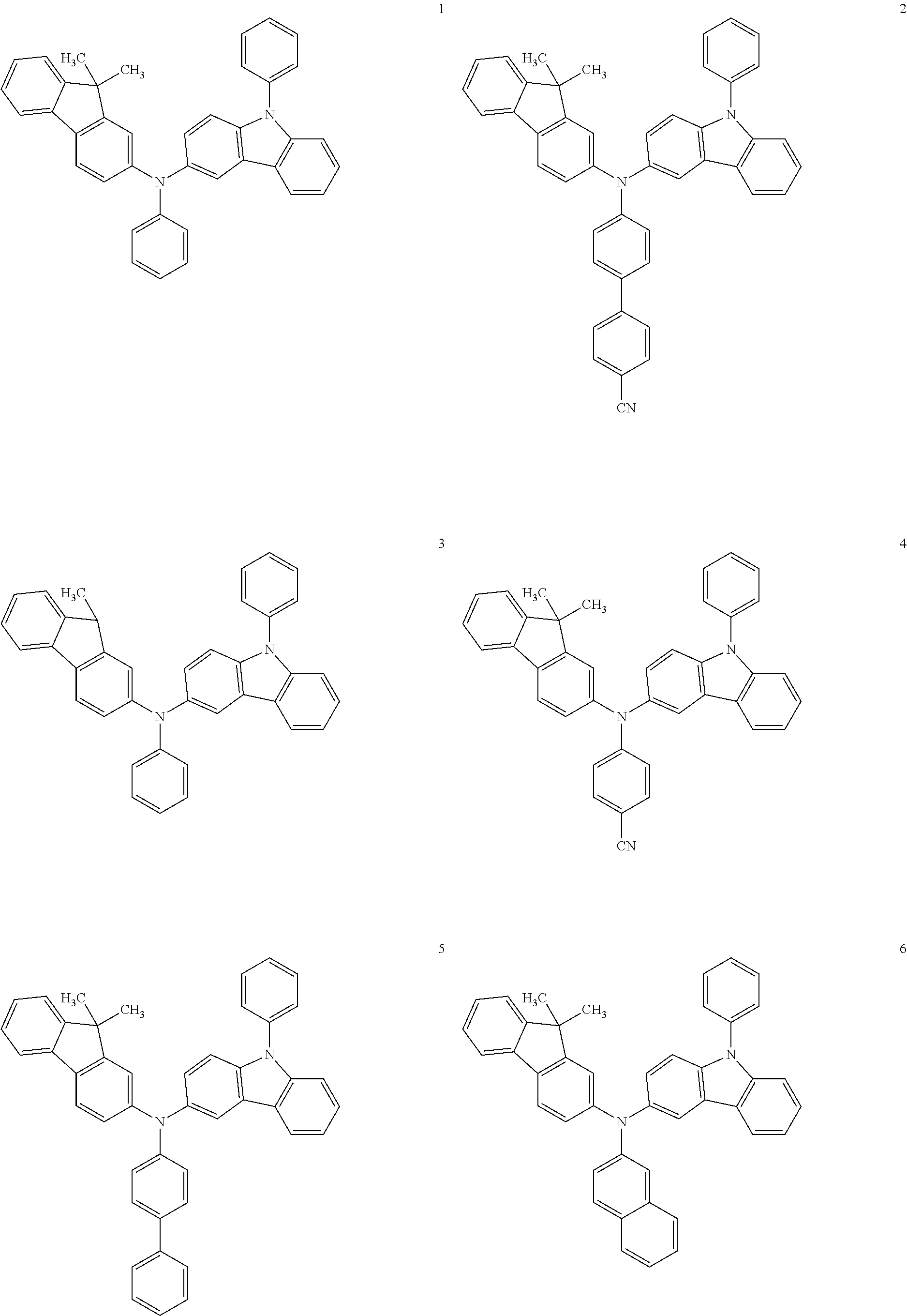


- The charge generating material is material generating charge carriers (i.e., holes and/or electrons) upon exposure to light. The charge generating material may include a compound represented by
Formula 3 below. -

- In
Formula 3, R51 to R56 are each independently selected from the group consisting of a hydrogen atom, —CN, —SOR100, —SON(R101)2, —SO 2R102, —SO2N(R103)2, —SO3R104, —SO3N(R105)2, —NO2, —CFH2, —CF2H, and —CF3, and R100 to R105 are each independently selected from the group consisting of a hydrogen atom, a substituted or unsubstituted C1-C30 alkyl group, a substituted or unsubstituted C5-C30 aryl group, and a substituted or unsubstituted C4-C30 heteroaryl group. - For example, R100 through R105 may be each independently selected from the group consisting of a hydrogen atom, a substituted or unsubstituted C1-C10 alkyl group, a substituted or unsubstituted C5-C14 aryl group, and a substituted or unsubstituted C4-C14 heteroaryl group.
- For example, R100 to R105 may be each independently selected from the group consisting of a hydrogen atom, a methyl group, an ethyl group, a propyl group, a butyl group, a pentyl group, a methyl group substituted with at least one —CN group, an ethyl group substituted with at least one —CN group, a propyl group substituted with at least one —CN, a butyl group substituted with at least one —CN, a pentyl group substituted with at least one —CN, a phenyl group, a naphthyl group, an anthryl group, a fluorenyl group, a phenyl group substituted with at least one —CN, a naphthyl group substituted with at least one —CN, an anthryl group substituted with at least one —CN, a fluorenyl group substituted with at least one —CN, a carbazolyl group, a quinolinyl group, an imidazolyl group, a carbazolyl group substituted with at least one —CN, a quinolinyl group substituted with at least one —CN, and an imidazolyl group substituted with at least one —CN, but are not limited thereto.
- For example, the charge generating material may be Compound 40 below, but is not limited thereto.
-

- The thicknesses of the
first HTL 141, thethird HTL 143, and thefifth HTL 145 may be each independently in the range of about 0.1 nm to about 100 nm. For example, the thicknesses of thefirst HTL 141 and thefifth HTL 145 may be each independently in the range of about 10 nm to about 100 nm, for example, about 50 mn to about 60 nm, but are not limited thereto. For example, the thickness of thethird HTL 143 may be in the range of about 0.5 nm to about 100 nm, for example, about 0.5 nm to about 10 nm, but is not limited thereto. - When the thicknesses of the
first HTL 141, thethird HTL 143, and thefifth HTL 145 are within this range of about 0.1 nm to about 100 nm, holes may be effectively injected and transported to theEML 150 without a substantial increase in driving voltage. The thicknesses of thefirst HTL 141, thethird HTL 143, and thefifth HTL 145 may be the same or different. - The thicknesses of the
second HTL 142 and thefourth HTL 144 may be each independently in the range of about 0.01 nm to about 16 nm, for example, about 0.5 nm to about 1 nm. When the thicknesses of thesecond HTL 142 and thefourth HTL 144 are within this range of about 0.01 nm to about 16 nm, holes may be effectively injected and transported to theEML 150 without a substantial increase in driving voltage. The thicknesses of thesecond HTL 142 and thefourth HTL 144 may be the same or different. - The amount of the charge generating material contained in the
second HTL 142 may be in the range of about 0.01 to about 99 parts by weight, for example, about 45 to about 55 parts by weight based on 100 parts by weight of thesecond HTL 142. The amount of the charge generating material contained in the fourth.HTL 144 may be in the range of about 0.01 to about 99 parts by weight, for example, about 45 to about 55 parts by weight based on 100 parts by weight of thefourth HTL 144. When the amount of the charge generating material contained in thesecond HTL 142 and thefourth HTL 144 is within the range of about 0.01 to about 99 parts by weight, the efficiency ofOLED 100 may be improved. - The
HTL 140 may be formed by using vacuum deposition, spin coating, casting, or the like. When theHTL 140 is formed using vacuum deposition or spin coating, the deposition and coating conditions may be similar to those for the formation of theHIL 130, though the deposition and coating conditions may vary according to the material that is used to form theHTL 140. - Using vacuum deposition, the
HTL 140 may be formed by preparing a first deposition source releasing the hole transporting material and a second deposition source releasing the charge generating material, disposing the first deposition source and the second deposition source to be spaced apart from each other such that a region to which the hole transporting material is released overlaps a region to which the charge generating material is released, and performing one reciprocation of the first and second deposition sources from a first end to a second end, and then from the second end to the first end of a region on which theHTL 140 will be formed on theHIL 130 inFIG. 1 . -
FIGS. 5A to 5G schematically illustrate a method of forming aHTL 140 on theHIL 130, according to an embodiment of the present invention. Although thesubstrate 110 and thefirst electrode 120 are disposed at one surface of theHIL 130 on which theHTL 140 is not formed, they are not shown inFIGS. 5A to 5G for descriptive convenience. - Referring to
FIG. 5A , afirst deposition source 1001 and asecond deposition source 1002 may be disposed below one surface of theHIL 130, i.e., the surface on which thesubstrate 110 and thefirst electrode 120 are not formed. Thefirst deposition source 1001 may be a deposition source releasing the hole transporting material, and thesecond deposition source 1002 may be a deposition source releasing the charge generating material. As shown inFIG. 5A , a region C1 to which the hole transporting material is released by thefirst deposition source 1001 and a region C2 to which the charge generating material is released by thesecond deposition source 1002 may have a fan shape with a predetermined angle. - Meanwhile, the
first deposition source 1001 and thesecond deposition source 1002 are disposed to be spaced apart from each other such that the region C1 to which the hole transporting material is released overlaps the region C2 to which the charge generating material is released. Accordingly, the hole transporting material and the charge generating material may be simultaneously deposited to form thesecond HTL 142 and thefourth HTL 144 including both of the hole transporting material and the charge generating material as shown inFIGS. 5B and 5F . - The
first deposition source 1001 and thesecond deposition source 1002 may be mounted on abase 1006 that is disposed on aguide rail 1005 that is disposed in a chamber and reciprocates along theguide rail 1005. Thebase 1006 may be connected to a separate drive unit (not shown) to operate. - As described above, the
base 1006 on which thefirst deposition source 1001 and thesecond deposition source 1002 are mounted to be spaced apart from each other by a predetermined distance may move in the B direction from a first end A below theHIL 130 when thefirst deposition source 1001 and thesecond deposition source 1002 are in an “on” state as shown inFIG. 5A . In this regard, only the hole transporting material is deposited on theHIL 130 to form thefirst HTL 141 including the hole transporting material (D1). Thefirst HTL 141 is continuously deposited toward a second end E below theHIL 130 as thebase 1006 moves in the B direction. - Then, as the
base 1006 on which thefirst deposition source 1001 and thesecond deposition source 1002 are mounted continuously moves in the B direction, a region (D2) on which the hole transporting material and the charge generating material are simultaneously deposited is formed to form thesecond HTL 142, including the hole transporting material and the charge generating material, on thefirst HTL 141 as shown inFIG. 5B . Thesecond HTL 142 is continuously deposited toward the second end E with respect to the second end E (SeeFIG. 5D ) as thebase 1006 moves in the B direction. - Then, as the
base 1006 on which thefirst deposition source 1001 and thesecond deposition source 1002 are mounted continuously moves in the B direction, a first charge generating material-containinglayer 143′ (D3) is formed on thesecond HTL 142 as shown inFIG. 5C . - As the
base 1006 on which thefirst deposition source 1001 and thesecond deposition source 1002 are mounted continuously moves in the B direction and arrives at the second end E of theHIL 130, thefirst HTL 141 including the hole transporting material, thesecond HTL 142 including the hole transporting material and the charge generating material, and the first charge generating material-containinglayer 143′ are formed on theHIL 130 as shown inFIG. 5D . - Then, the
base 1006 that arrived at the second end E below theHIL 130 changes its direction to start to move in the F direction opposite to the B direction as shown inFIG. 5E . In this regard, a second charge generating material-containinglayer 143″ is first formed as shown inFIG. 5E . - As the
base 1006 continuously moves in the F direction, thefourth HTL 144 including the hole transporting material and the charge generating material and thefifth HTL 145 including the hole transporting material are sequentially formed on the second charge generating material-containinglayer 143″ as shown inFIG. 5F . Here, the first charge generating material-containinglayer 143′ and the second charge generating material-containinglayer 143″ have the same component, i.e., the charge generating material, the interface between the first charge generating material-containinglayer 143′ and the second charge generating material-containinglayer 143″ may not be clearly distinguished, so that they may be seen as a single layer, i.e., thethird HTL 143 including the charge generating material. Thus, the interface between the first charge generating material-containinglayer 143′ and the second charge generating material-containinglayer 143″ is shown as a dash line instead of a solid line inFIG. 5F . - When the
base 1006 on which thefirst deposition source 1001 and thesecond deposition source 1002 are mounted arrives at the first end A, thefirst HTL 141 including the hole transporting material, thesecond HTL 142 including the hole transporting material and the charge generating material, thethird HTL 143 including the charge generating material, thefourth HTL 144 including the hole transporting material and the charge generating material, and thefifth HTL 145 including the hole transporting material may be sequentially formed on theHIL 130 as shown inFIG. 5G . In this regard, although thethird HTL 143 includes two charge generating material-containing layers, i.e., the first charge generating material-containinglayer 143′ and the second charge generating material-containinglayer 143″, an interface S′ between the first charge generating material-containinglayer 143′ and the second charge generating material-containinglayer 143″ is not clearly distinguished, so that they may be seen as a single layer. Thus, the interface S′ is shown as a dash line inFIG. 5G - According to the method of forming the
HTL 140 as described above, theHTL 140 including one hole transport unit having thefirst HTL 141, thesecond HTL 142, thethird HTL 143, thefourth HTL 144, and thefifth HTL 145 may be prepared by one reciprocation of thebase 1006 on which thefirst deposition source 1001 and thesecond deposition source 1002 are mounted from the first end A to the second end E, and then from the second end E to the first end A. In other words, one hole transport unit may be formed using the method of forming the layers shown inFIG. 5A to 5G . Thus, the stacking process is simply and quickly performed, and a plurality of layers may be simultaneously deposited in a single chamber without evacuating the chamber between the formations of the layers. - The
EML 150 may be formed on theHTL 140 by vacuum deposition, spin coating, casting, LB deposition, or the like. When theEML 150 is formed by vacuum deposition or spin coating, the conditions for deposition and coating are similar to those for the formation of theHIL 130, although the conditions for deposition and coating may vary according to the material that is used to form theEML 150. - The
EML 150 may be formed of a compound, or a combination of a host and a dopant. Examples of the host include, but are not limited to, Alq3, 4,4′-N,N′- dicarbazole-biphenyl (CBP), poly(n-vinylcarbazole) (PVK), 9,10-di(naphthalene-2-yl)anthracene (ADN), TCTA, 1,3.5-tris(N-phenylbenzimidazole-2-yl)benzene (TPBI), 3-tert-butyl-9,10-di-2-naphthyl anthracene (TBADN), E3, distyrylarylene (DSA), bis(2-(2-hydroxyphenyl)benzothiazolate)zinc (Zn(BTZ)2), Compound 51 below, and Compound 52 below. -


- Meanwhile, examples of known red dopants include PtOEP, Ir(piq)3, and Btp2Ir(acac), but are not limited thereto.
-

- Examples of green dopants include Ir(ppy)3 (ppy=phenylpyridine), Ir(ppy)2(acac), Ir(mpyp)3, and Compound 53 below, but are not limited thereto.
-

- Meanwhile, examples of known blue dopants include F2Irpic, (F2ppy)2Ir(tmd), Ir(dfppz)3, ter-fluorene, 4,4′-bis(4-diphenyl aminostyryl)biphenyl (DPAVBi), 2,5,8,11-tetra-tert-butyl perylene (TBPe), Compound 54 below, and 4,4′-bis(2,2-diphenylethenyl)biphenyl (DPVBi).
-

- When a dopant and a host are used together, the amount of the dopant may be in the range of about 0.01 to about 15 parts by weight based on 100 parts by weight of the host, but is not limited thereto.
- The thickness of the
EML 150 may be in the range of about 100 to about 1,000 Å, for example, about 200 to about 600 Å. When the thickness of theEML 150 is within this range of about 100 to about 1,000 Å, theEML 150 may have excellent light emitting ability without a substantial increase in driving voltage. - When a phosphorescent dopant is also used to form the
EML 150, a hole blocking layer (HBL) (not shown inFIG. 1 ) may be formed on theEML 150 by using vacuum deposition, spin coating, casting, LB deposition, or the like, in order to prevent diffusion of triplet excitons or holes into anETL 160. When the HBL is formed using vacuum deposition or spin coating, the conditions for deposition and coating may be similar to those for the formation of theHIL 130, although the conditions for deposition and coating may vary according to the material that is used to form the HBL. Any material that is commonly used to form a HBL may be used. Examples of materials for forming the HBL include an oxadiazole derivative, a triazole derivative, and a phenanthroline derivative, but are not limited thereto. - The thickness of the HBL may be in a range of about 50 to about 1,000 Å, for example, about 100 to about 300Å. When the thickness of the HBL is within this range of about 50 to about 1,000 Å, the HBL may have excellent hole blocking ability without a substantial increase in driving voltage.
- The
ETL 160 is formed on theEML 150 or on the HBL if the HBL is formed. - The
ETL 160 includes an electron transporting material and a metal-containing material. - The electron transporting material may be any electron transporting material.
- The electron transporting material may be selected from the group consisting of Compound 60 and compounds represented by
Formulae -

- In
Formulae - L21 is a substituted or unsubstituted C1-C30 alkylene group, a substituted or unsubstituted C6-C30 arylene group, or a substituted or unsubstituted C3-C30 heteroarylene group;
- Q11 through Q19 are, each independently, a hydrogen atom, a substituted or unsubstituted C6-C30 aryl group, or a substituted or unsubstituted C3-C30 heteroaryl group; and
- c is an integer from 0 to 10.
- For example, R61 to R66 may be each independently selected from the group consisting of a hydrogen atom, a halogen atom, a hydroxyl group, a cyano group, a methyl group, an ethyl group, a propyl group, a butyl group, a methoxy group, an ethoxy group, a propoxy group, a butoxy group, a phenyl group, a naphthyl group, an anthryl group, a pyridinyl group, and a pyrazinyl group, but are not limited thereto.
- In particular, in
Formula 4 and 5 R61 to R64 may be hydrogen atoms, and R65 may be selected from the group consisting of a halogen atom, a hydroxyl group, a cyano group, a methyl group, an ethyl group, a propyl group, a butyl group, a methoxy group, an ethoxy group, a propoxy group, a butoxy group, a phenyl group, a naphthyl group, an anthryl group, a pyridinyl group, and a pyrazinyl group. In addition, inFormula 4 and 5 R61 to R66 may be hydrogen atoms, but are not limited thereto. - For example, Q11 and Q19 may be each independently selected from the group consisting of a hydrogen atom, a phenyl group, a naphthyl group, an anthryl group, a pyridinyl group, and a pyrazinyl group, but are not limited thereto.
- In particular, in
Formulae - For example, L21 may be selected from the group consisting of a phenylene group, a naphthylene group, an anthrylene group, a pyridinylene group, and a pyrazinylene group, but is not limited thereto. For example, L21 may be a phenylene group or a pyridinylene group.
- For example, c may be 1, 2, or 3, but is not limited thereto.
- The electron transport material may be Compound 60 shown above or Compound 61 or 62 below.
-

- The metal-containing material may inject electrons and block holes. For this, the metal-containing material may be a Li complex.
- For example, the metal-containing material may be lithium quinolate (LiQ) or Compound 81 below, but is not limited thereto.
-

- The thickness of the
ETL 160 may be in the range of about 50 to about 1,000 Å, for example, about 100 to about 300 Å. When the thickness of theETL 160 is within the range of about 50 to about 1,000 Å, an excellent electron transporting ability of theETL 160 may be obtained without a substantial increase in driving voltage. - The
EIL 180, which facilitates injection of electrons from the cathode (second electrode 190), may be formed on theETL 160. Examples of materials for forming theEIL 180 include LiF, NaCl, CsF, Li2O, and BaO, which are known in the art. Deposition and coating conditions for forming theEIL 180 are similar to those for the formation of theHIL 130, although the deposition and coating conditions may vary according to a material that is used to form theEIL 180. - The thickness of the
EIL 180 may be in the range of about 1 to about 100 Å, for example, about 5 to about 90 Å. When the thickness of theEIL 180 is within this range of about 1 to about 100 Å, theEIL 180 may have satisfactory electron injecting ability without a substantial increase in driving voltage. - The
second electrode 190 is disposed on theEIL 180. Thesecond electrode 190 may be a cathode, which is an electron injecting electrode. A metal for forming thesecond electrode 190 may be a metal, an alloy, an electrically conductive compound, which have a low-work function, or a mixture thereof. In this regard, thesecond electrode 190 may be a reflective electrode formed of lithium (Li), magnesium (Mg), aluminum (Al), aluminum (Al)-lithium (Li), calcium (Ca), magnesium (Mg)-indium (In), magnesium (Mg)-silver (Ag), or the like. Alternatively, thesecond electrode 190 may be a transmissive or semi-transmissive electrode formed of a transparent conductive material such as ITO and IZO. - The
HTL 140 of theOLED 100 has a multi-layered structure, in which energy levels of the layers are similar to each other, and theETL 160 includes the electron transporting material and the metal-containing material. Thus, the balance in the flow of holes and electrons is maintained for a long period of time, the injection and transport of electrons are adjusted, and holes are blocked, so that theOLED 100 may have long lifetime. -
FIG. 2 is a schematic cross-sectional view of anOLED 200 according to another embodiment of the present invention. - Referring to
FIG. 2 , theOLED 200 according to the current embodiment of the present invention includes asubstrate 210, and afirst electrode 220, aHIL 230, aHTL 240, anEML 250, anETL 260, anEIL 280, and asecond electrode 290 which are sequentially stacked on thesubstrate 210 in the order stated. - The
HTL 240 include two hole transport units, i.e., a firsthole transport unit 240 a and a second hole transport unit 240 b. In particular, theHTL 240 includes: the firsthole transport unit 240 a including afirst HTL 241 having a hole transporting material; asecond HTL 242 formed on thefirst HTL 241 and having the hole transporting material and a charge generating material; athird HTL 243 formed on thesecond HTL 242 and having the charge generating material; afourth HTL 244 formed on thethird HTL 243 and having the hole transporting material and the charge generating material; and afifth HTL 245 formed on thefourth HTL 244 and having the hole transporting material; and the second hole transport unit 240 b including asixth HTL 246 formed on thefifth HTL 245 and having the hole transporting material; aseventh HTL 247 formed on thesixth HTL 246 and having the hole transporting material and the charge generating material; aneighth HTL 248 formed on theseventh HTL 247 and having the charge generating material; aninth HTL 249 formed on theeighth HTL 248 and having the hole transporting material and the charge generating material; and atenth HTL 249 b formed on theninth HTL 249 and having the hole transporting material. - Since the
HTL 240 includes two hole transport units, i.e., the firsthole transport unit 240 a and the second hole transport unit 240 b, the method of forming the layers described with reference toFIGS. 5A to 5G may be repeated twice to prepare theHTL 240. In other words, thebase 1006 on which thefirst deposition source 1001 and thesecond deposition source 1002 are mounted is reciprocated twice along theguide rail 1005. For example, theHTL 240 may be formed by the following process: start from the first end A→move in the B direction→arrive at the second end E→move in the F direction→arrive at the first end A→move in the B direction→arrive at the second end E→move in the F direction→arrive at the first end A. - When the
HTL 240 is formed using the method described above, thethird HTL 243 includes two charge generating material-containing layers, i.e., a first charge generating material-containinglayer 243′ and a second charge generating material-containinglayer 243″, and components of the two layers are the same as the charge generating material. Thus, the interface between the first charge generating material-containinglayer 243′ and the second charge generating material-containinglayer 243″ is not clearly distinguished, so that thethird HTL 243 may be seen as a single layer. Similarly, theeighth HTL 248 includes two charge generating material-containing layers, i.e., a first charge generating material-containinglayer 248′ and a second charge generating material-containinglayer 248″, and components of the two layers are the same as the charge generating material. Thus, the interface between the first charge generating material-containinglayer 248′ and the second charge generating material-containinglayer 248″ is not clearly distinguished, so that theeighth HTL 248 may be seen as a single layer. Thus, the interface between the first charge generating material-containinglayer 243′ and the second charge generating material-containinglayer 243″ of thethird HTL 243 and the interface between the first charge generating material-containinglayer 248′ and the second charge generating material-containinglayer 248″ of theeighth HTL 248 are shown as a dash line instead of a solid line inFIG. 2 . - Meanwhile, the interface between the
fifth HTL 245 and thesixth HTL 246 is shown as a dash line inFIG. 2 . Since the component of the fifth HTL 245 (hole transporting material) formed after the first reciprocation of the base 1006 (start from the first end A→move in the B direction→arrive at the second end E→move in the F direction→arrive at the first end A) is the same as the component of the sixth HTL 246 (hole transporting material) formed by the second reciprocation of the base 1006 that starts from the first end A after the first reciprocation, the interface between thefifth HTL 245 and thesixth HTL 246 is not clearly distinguished, and thus thefifth HTL 245 and thesixth HTL 246 may be seen as a single layer. - The
OLED 200 ofFIG. 2 has the same structure as theOLED 100 ofFIG. 1 , except that theOLED 200 includes theHTL 240 having two hole transport units instead of one hole transport unit, and thus the material used to form each layer and the thickness of each layer of theOLED 200 are defined as described above with reference toFIG. 1 . -
FIG. 3 is a schematic cross-sectional view of anOLED 300 according to another embodiment of the present invention. - Referring to
FIG. 3 , theOLED 300 according to the current embodiment includes asubstrate 310, and afirst electrode 320, aHIL 330, aHTL 340, anEML 350, anETL 360, anEIL 380, and asecond electrode 390 which are sequentially stacked on thesubstrate 310 in the order stated. - The
HTL 340 include two hole transport units, i.e., a firsthole transport unit 340 a and a secondhole transport unit 340 b. In particular, theHTL 340 includes: the firsthole transport unit 340 a including afirst HTL 341 having a hole transporting material; asecond HTL 342 formed on thefirst HTL 341 and having the hole transporting material and a charge generating material; athird HTL 343 formed on thesecond HTL 342 and having the charge generating material; afourth HTL 344 formed on thethird HTL 343 and having the hole transporting material and the charge generating material; and afifth HTL 345 formed on thefourth HTL 344 and having the hole transporting material; and the secondhole transport unit 340 b including asixth HTL 346 formed on thefifth HTL 345 and having a hole transporting material; aseventh HTL 347 formed on thesixth HTL 346 and having the hole transporting material and the charge generating material; aneighth HTL 348 formed on theseventh HTL 347 and having the charge generating material; aninth HTL 349 formed on theeighth HTL 348 and having the hole transporting material and the charge generating material; and atenth HTL 349 b formed on theninth HTL 349 and having the hole transporting material. - The
HTL 340 is defined as theHTL 240 described above. - The
ETL 360 includes one electron transport unit including: afirst ETL 361 having an electron transporting material; asecond ETL 362 formed on thefirst ETL 361 and having the electron transporting material and the metal-containing material; athird ETL 363 formed on thesecond ETL 362 and having the metal-containing material; afourth ETL 364 formed on thethird ETL 363 and having the electron transporting material and the metal-containing material; and afifth ETL 365 formed on thefourth ETL 364 and having the electron transporting material. - The
ETL 360 has a structure in which thesecond ETL 362, thethird ETL 363, thefourth ETL 364, and the fifth.ETL 365 are sequentially stacked on thefirst ETL 361 in the order stated, so that injection and transport of electrons may be controlled and holes may be blocked. In theOLED 300, the number of excitons generated in emission regions may be gradually reduced since the amount of electrons or holes may change with time during the operation of theOLED 300. As a result, a carrier balance may not be maintained, and thus, the lifetime of theOLED 300 may be reduced. However, since theETL 360 has a stack structure of a plurality of layers with a similar or same energy level (thefirst ETL 361, thesecond ETL 362, thethird ETL 363, thefourth ETL 364, and the fifth ETL 365), the flow of carriers may be constantly maintained while controlling migration rates of electrons. Thus, lifetime characteristics of theOLED 300 may be improved. - The
ETL 360 may be formed by preparing a third deposition source releasing the electron transporting material and a fourth deposition source releasing the metal-containing material, disposing the third deposition source and the fourth deposition source to be spaced apart from each other such that a region to which the electron transporting material is released overlaps a region to which the metal-containing material is released, and performing one reciprocation of the third and fourth deposition sources from a first end to a second end, and then from the second end to the first end of a region on which theETL 360 will be formed (on the EML 350). - The method of forming the
ETL 360 may be easily understood by the descriptions above with reference toFIGS. 5A to 5G and replacing the hole transporting material with the electron transporting material, replacing the charge generating material with the metal-containing material, replacing the first deposition source with the third deposition source, and replacing the second deposition source with the fourth deposition source. - As described above, when the
ETL 360 is formed, a first metal-containing material-containinglayer 363′ and a second metal-containing material-containinglayer 363″ have the same component, i.e., the metal-containing material, the interface between the first metal-containing material-containinglayer 363′ and the second metal-containing material-containinglayer 363″ may not be clearly distinguished, so that they may be seen as a single layer, i.e., thethird ETL 363 including the metal-containing material. Thus, the interface between the first metal-containing material-containinglayer 363′ and the second metal-containing material-containinglayer 363″ is shown as a dash line instead of a solid line inFIG. 3 . - The thicknesses of the
first ETL 361, thethird ETL 363, and thefifth ETL 365 may be each independently in the range of about 0.01 nm to about 1 nm, for example, about 0.5 nm to about 0.7 nm. When the thicknesses of thefirst ETL 361, thethird ETL 363, and thefifth ETL 365 are within this range of about 0.01 nm to about 1 nm, electrons may effectively be injected and transported to theEML 350 without a substantial increase in driving voltage. The thicknesses of thefirst ETL 361, thethird ETL 363, and thefifth ETL 365 may be the same or different. - The thicknesses of the
second ETL 362 and thefourth ETL 364 may be each independently a thickness in the range of about 6 nm to about 16 nm, for example, about 6 nm to about 10 nm. When the thicknesses of thesecond ETL 362 and thefourth ETL 364 are within this range of about 6 nm to about 16 nm, electrons may effectively be injected and transported to theEML 350 without a substantial increase in driving voltage. The thicknesses of thesecond ETL 362 and thefourth ETL 364 may be the same or different. - The amount of the metal-containing material contained in the
second ETL 362 may be in the range of about 20 to about 80 parts by weight, for example, about 45 to about 55 parts by weight based on 100 parts by weight of thesecond ETL 362. The amount of the metal-containing material contained in thefourth ETL 364 may be in the range of about 20 to about 80 parts by weight, for example, about 45 to about 55 parts by weight based on 100 parts by weight of thefourth ETL 364. When the amount of the metal-containing material contained in thesecond ETL 362 and thefourth ETL 364 is within the range of about 20 to about 80 parts by weight, the efficiency ofOLED 300 may be improved. - The electron transporting material and the metal-containing material of the
ETL 360 are defined as described above with reference toFIG. 1 . - The
OLED 300 ofFIG. 3 has the same structure as theOLED 200 ofFIG. 2 , except that theOLED 300 includes theETL 360 having a multi-layered structure, and thus the material used to form each layer and the thickness of each layer of theOLED 300 are defined as described above with reference toFIGS. 1 and 2 . -
FIG. 4 is a schematic cross-sectional view of an OLED 400 according to another embodiment of the present invention. - Referring to
FIG. 4 , the OLED 400 according to the current embodiment of the present invention includes a substrate 410, and a first electrode 420, a HIL 430, a HTL 440, an EML 450, an ETL 460, an EIL 480, and a second electrode 490 which are sequentially stacked on the substrate 410 in the order stated. - The HTL 440 include two hole transport units, i.e., a first hole transport unit 440 a and a second hole transport unit 440 b. In particular, the HTL 440 includes: the first hole transport unit 440 a including a first HTL 441 having a hole transporting material; a second HTL 442 formed on the first HTL 441 and having the hole transporting material and a charge generating material; a third HTL 443 formed on the second HTL 442 and having the charge generating material; a fourth HTL 444 formed on the third HTL 443 and having the hole transporting material and the charge generating material; and a fifth HTL 445 formed on the fourth HTL 444 and having the hole transporting material; and the second hole transport unit 440 b including a sixth HTL 446 formed on the fifth HTL 445 and having a hole transporting material; a seventh HTL 447 formed on the sixth HTL 446 and having the hole transporting material and the charge generating material; an eighth HTL 448 formed on the seventh HTL 447 and having the charge generating material; a ninth HTL 449 formed on the eighth HTL 448 and having the hole transporting material and the charge generating material; and a tenth HTL 449 b formed on the ninth HTL 449 and having the hole transporting material.
- The HTL 440 is defined as the
HTL 240 described above. - The ETL 460 includes two electron transport units, i.e., a first electron transport unit 460 a and a second electron transport unit 460 b. In particular, the ETL 460 includes: the first electron transport unit 460 a including a first ETL 461 having an electron transporting material; a second ETL 462 formed on the first ETL 461 and having the electron transporting material and the metal-containing material; a third ETL 463 formed on the second ETL 462 and having the metal-containing material; a fourth ETL 464 formed on the third ETL 463 and having the electron transporting material and the metal-containing material; and a fifth ETL 465 formed on the fourth ETL 464 and having the electron transporting material; and the second electron transport unit 460 b including a sixth ETL 466 formed on the fifth ETL 465 and having the electron transporting material; a seventh ETL 467 formed on the sixth ETL 466 and having the electron transporting material and the metal-containing material; a eighth ETL 468 formed on the seventh ETL 467 and having the metal-containing material; a ninth ETL 469 formed on the eighth ETL 468 and having the electron transporting material and the metal-containing material; and a tenth ETL 469 b formed on the ninth ETL 469 and having the electron transporting material.
- Since the ETL 460 includes two electron transport units, i.e., the first electron transport unit 460 a and the second electron transport unit 460 b, the method of forming the layers described with reference to
FIGS. 5A to 5G may be repeated twice to prepare the ETL 460 and replacing the hole transporting material with the electron transporting material, replacing the charge generating material with the metal-containing material, replacing the first deposition source with the third deposition source, and replacing the second deposition source with the fourth deposition source. - When the ETL 460 is formed using the method described above, the third ETL 463 includes two metal-containing, material-containing layers, i.e., a first metal-containing material-containing layer 463′ and a second metal-containing material-containing layer 463″, and components of the two layers are the same as the metal-containing material. Thus, the interface between the first metal-containing material-containing layer 463′ and the second metal-containing material-containing layer 463″ is not clearly distinguished, so that the third ETL 463 may be seen as a single layer. Similarly, the eighth ETL 468 may be seen as a single layer.
- Meanwhile, the interface between the fifth ETL 465 and the sixth ETL 466 is shown as a dash line in
FIG. 4 . Since the component of the fifth ETL 465 (electron transporting material) formed after the first reciprocation of the base 1006 (start from the first end A move in the B direction arrive at the second end E move in the F direction arrive at the first end A) is the same as the component of the sixth ETL 466 (electron transporting material) formed by the second reciprocation of the base 1006 that starts from the first end A after the first reciprocation, the interface between the fifth ETL 465 and the sixth ETL 466 is not clearly distinguished, and thus the fifth ETL 465 and the sixth ETL 466 may be seen as a single layer. - The OLED 400 of
FIG. 4 has the same structure as theOLED 300 ofFIG. 3 , except that the OLED 400 includes the ETL 460 having two electron transport units instead of one electron transport unit, and thus the material used to form each layer and the thickness of each layer of the OLED 400 are defined as described above with reference toFIGS. 1 , 2, and 3. -
FIG. 6 is a schematic sectional view of anOLED 10 according to another embodiment of the present invention. Referring toFIG. 6 , theOLED 10 according to the current embodiment of the present invention includes asubstrate 11, and afirst electrode 12, aHIL 13, aHTL 14, anEML 15, anETL 16, anEIL 18, and asecond electrode 19 which are sequentially stacked on thesubstrate 11 in the order stated. TheHTL 14 includes one hole transport unit including: afirst HTL 14 a having a hole transporting material; athird HTL 14 b formed on thefirst HTL 14 a and having a charge generating material; and afifth HTL 14 c formed on thethird HTL 14 b and having the hole transporting material. - In the
OLED 10, thesubstrate 11, thefirst electrode 12, theHIL 13, theEML 15, theETL 16, theEIL 18, and thesecond electrode 19 are defined as described above with reference toFIG. 1 . - The
HTL 14 includes thefirst HTL 14 a, thethird HTL 14 b, and thefifth HTL 14 c which are defined as described above with reference tofirst HTL 141, thethird HTL 143, and thefifth HTL 145 ofFIG. 1 . That is, theOLED 10 ofFIG. 6 has the same structure as theOLED 100 ofFIG. 1 , except that theOLED 10 does not include thesecond HTL 142 and thefourth HTL 144 ofFIG. 1 . - The
third HTL 14 b of theOLED 10 may include the charge generating material as described above. Thethird HTL 14 b may include a first charge generating material-containinglayer 14 b′ and a second charge generating material-containinglayer 14 b″. The interface S′ between the first charge generating material-containinglayer 14 b′ and the second charge generating material-containinglayer 14 b″ is not clearly distinguished, so that they may be seen as a single layer, i.e. thethird HTL 14 b including the charge generating material. Thus, the interface between the first charge generating material-containinglayer 14 b′ and the second charge generating material-containinglayer 14 b″ is shown as a dash line instead of a solid line inFIG. 5F . - The
HTL 14 has a structure in which thefirst HTL 14 a, thethird HTL 14 b, and thefifth HTL 14 c are sequentially stacked, so that injection and transport of holes may be controlled and electrons may be blocked. Accordingly, lifetime characteristics of theOLED 10 may be improved. - The
HTL 14 of theOLED 10 may be formed by preparing thebase 1006 on which thefirst deposition source 1001 and thesecond deposition source 1002 are mounted, as shown inFIG. 5A , disposing a anti-deposition plate between thefirst deposition source 1001 and thesecond deposition source 1002, and reciprocating thebase 1006 once according to the following process: start from the first end A→move in the B direction→arrive at the second end E→move in the F direction→arrive at the first end A. As described above, since the anti-deposition plate is disposed between thefirst deposition source 1001 and thesecond deposition source 1002, the simultaneous deposition of the hole transporting material released from thefirst deposition source 1001 and the charge generating material released from thesecond deposition source 1002 is substantially prevented, and thus thefirst HTL 14 a, thethird HTL 14 b, and thefifth HTL 14 c may be sequentially stacked. - The OLED and the method of manufacturing the OLED according to an embodiment of the present invention are described with reference to
FIGS. 1 , 2, 3, 4, 5 a to 5 g, and 6, but are not limited thereto, and various modifications may be applied thereto. For example, the HTL of the OLED according to an embodiment may include three or more hole transport units and/or the ETL of the OLED may include three or more electron transport units, and various modifications may be applied thereto. In addition, if desired, the HTL may be formed on the first electrode without forming the HIL, and various modifications may be applied thereto. - The HTL and the ETL described above may also be combined with each other. For example, an OLED including the
HTL 14 of theOLED 10 shown inFIG. 6 and theETL 360 of theOLED 300 inFIG. 3 may also be manufactured. - Meanwhile, even though not shown in
FIGS. 1 to 4 , a sealing layer may further be formed on the second electrode in order to seal the OLED, and various modifications may be applied thereto. - Hereinafter, one or more embodiments will be described in detail with reference to the following examples. These examples are not intended to limit the purpose and scope of the one or more embodiments of the present invention.
- A glass substrate including a 150 Ωcm2 (70 Å) ITO (a first electrode) (available from Corning Co.) was cut to a size of 50 mm×50 mm×0.5 mm, ultrasonically washed with isopropyl alcohol for 5 minutes and then with pure water for 5 minutes, heat-treated for 30 minutes, and treated with N2 plasma. A HTL was formed on the ITO
electrode using Compound 14 as a hole injecting and transporting material and Compound 40 as a charge generating material by using the method described with reference toFIGS. 5A to 5G , by which thefirst deposition source 1001 emitsCompound 14 and thesecond deposition source 1002 emits Compound 40 while thebase 1006 reciprocates once (start from the first end A→move in the B direction→arrive at the second end E→move in the F direction→arrive at the first end A). As a result, a HTL including one hole transport unit including a first HTL formed ofCompound 14 and having a thickness of 600 Å, a second HTL formed ofCompound 14 and Compound 40 and having a thickness of 10 Å, a third HTL formed of Compound 40 and having a thickness of 30 Å, a fourth HTL formed ofCompound 14 and Compound 40 and having a thickness of 10 Å, and a fifth HTL formed ofCompound 14 and having a thickness of 600 Å was prepared. 97 wt % of Alq3 as a host and 3 wt % of DPVBI as a dopant were deposited on the HTL to form an. EML having a thickness of 200 Å. Compound 62 and LiQ were co-deposited on the EML to form an ETL having a thickness of 300 Å, wherein the amount of LiQ was 50 parts by weight based on 100 parts by weight of the ETL, and LiF was vacuum-deposited on the ETL to form an EIL having a thickness of 5 Å. Then, Mg and Ag were vacuum-deposited on the EIL to form a second electrode having a thickness of 120 Å, and Alq3 was vacuum-deposited on the second electrode to form an organic capping layer, thereby completing the manufacture of an OLED. -

-
FIG. 7 is a graph illustrating time-brightness of an OLED according to Example 1. InFIG. 7 , the Y-axis indicates brightness (%). When the time is zero (0), the brightness is 100%. The brightness was evaluated using a PR650 (Spectroscan) Source Measurement Unit. (PhotoResearch).FIG. 8 is a graph illustrating voltage-current density of the OLED according to Example 1. InFIG. 8 , the X-axis indicates voltage (V), and the Y-axis indicates current density (mA/cm2). Referring toFIGS. 7 and 8 , the OLED manufactured according to Example 1 has excellent electrical and lifetime characteristics. - It should be understood that the exemplary embodiments described therein should be considered in a descriptive sense only and not for purposes of limitation. Descriptions of features or aspects within each embodiment should typically be considered as available for other similar features or aspects in other embodiments.
Claims (20)


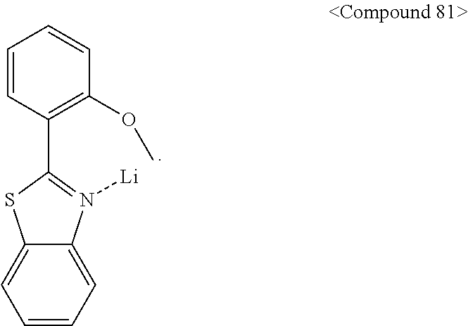
Applications Claiming Priority (2)
| Application Number | Priority Date | Filing Date | Title |
|---|---|---|---|
| KR10-2010-0020402 | 2010-03-08 | ||
| KR1020100020402A KR101097339B1 (en) | 2010-03-08 | 2010-03-08 | Organic light emitting diode and method for preparing the same |
Publications (2)
| Publication Number | Publication Date |
|---|---|
| US20110215308A1 true US20110215308A1 (en) | 2011-09-08 |
| US9472767B2 US9472767B2 (en) | 2016-10-18 |
Family
ID=43795135
Family Applications (1)
| Application Number | Title | Priority Date | Filing Date |
|---|---|---|---|
| US13/042,561 Active 2032-10-04 US9472767B2 (en) | 2010-03-08 | 2011-03-08 | Organic light-emitting device and method of manufacturing the same |
Country Status (5)
| Country | Link |
|---|---|
| US (1) | US9472767B2 (en) |
| EP (1) | EP2365555B1 (en) |
| JP (2) | JP2011187959A (en) |
| KR (1) | KR101097339B1 (en) |
| CN (1) | CN102201432B (en) |
Cited By (34)
| Publication number | Priority date | Publication date | Assignee | Title |
|---|---|---|---|---|
| US20120326135A1 (en) * | 2011-06-22 | 2012-12-27 | Young-Kook Kim | Heterocyclic compound and organic light-emitting diode and flat display device including the heterocyclic compound |
| WO2014056565A1 (en) * | 2012-10-09 | 2014-04-17 | Merck Patent Gmbh | Electronic device |
| US20140117337A1 (en) * | 2012-10-31 | 2014-05-01 | Lg Display Co., Ltd. | Light emitting device and organic light emitting display device including the same |
| CN103915470A (en) * | 2012-12-31 | 2014-07-09 | 乐金显示有限公司 | Organic light emitting display device |
| US20140361272A1 (en) * | 2013-06-07 | 2014-12-11 | Samsung Display Co., Ltd. | Light emitting element, organic light emitting display device having the same and method of manufacturing the same |
| US20150014645A1 (en) * | 2013-07-09 | 2015-01-15 | Samsung Display Co., Ltd. | Organic light-emitting device |
| US20150028308A1 (en) * | 2013-07-25 | 2015-01-29 | Samsung Display Co., Ltd. | Organic light emitting device, organic light emitting display apparatus having the organic light emitting device and method of manufacturing the same |
| US20150034923A1 (en) * | 2013-07-31 | 2015-02-05 | Lg Display Co., Ltd. | White organic light emitting diode device |
| US20150236267A1 (en) * | 2014-02-17 | 2015-08-20 | Samsung Display Co., Ltd. | Organic electroluminescence device |
| US20150255741A1 (en) * | 2014-03-06 | 2015-09-10 | Samsung Display Co., Ltd. | Organic light emitting diode device |
| US9224966B2 (en) | 2011-11-08 | 2015-12-29 | Samsung Display Co., Ltd. | Organic light-emitting device, method of manufacturing the same, and flat panel display device including the same |
| US20160079542A1 (en) * | 2014-09-09 | 2016-03-17 | Samsung Display Co., Ltd. | Organic electroluminescence device |
| US9299936B2 (en) | 2011-12-02 | 2016-03-29 | Samsung Display Co., Ltd. | Organic light-emitting diode including multi-layered hole transporting layer, and flat display device including the organic light-emitting diode |
| US20160111653A1 (en) * | 2014-10-21 | 2016-04-21 | Samsung Display Co., Ltd. | Organic electroluminescent material and organic electroluminescent device including the same |
| US20160141513A1 (en) * | 2014-11-14 | 2016-05-19 | Samsung Display Co., Ltd. | Organic light-emitting device |
| US20160163982A1 (en) * | 2014-12-03 | 2016-06-09 | Samsung Display Co., Ltd. | Organic electroluminescent device |
| US20160365515A1 (en) * | 2015-06-15 | 2016-12-15 | Samsung Display Co., Ltd. | Organic electroluminescent device |
| US20170012204A1 (en) * | 2015-07-08 | 2017-01-12 | Samsung Display Co., Ltd. | Material for organic electroluminescent device and organic electroluminescent device comprising same |
| US9559311B2 (en) | 2013-02-22 | 2017-01-31 | Idemitsu Kosan Co., Ltd. | Anthracene derivative, organic-electroluminescence-device material, organic electroluminescence device, and electronic equipment |
| TWI574949B (en) * | 2012-06-27 | 2017-03-21 | 三星顯示器有限公司 | Organic light-emitting device including multi-layered hole transport layer and organic light-emitting display apparatus including the same |
| US20170098793A1 (en) * | 2014-06-03 | 2017-04-06 | Sharp Kabushiki Kaisha | Organic el element and method for manufacturing same |
| US20170301876A1 (en) * | 2014-10-01 | 2017-10-19 | Novaled Gmbh | Organic Light-Emitting Diode Including an Electronic Transport Layer Comprising a Three Component Blend of a Matrix Compound and Two Lithium Compounds |
| US9812643B2 (en) | 2011-10-27 | 2017-11-07 | Merck Patent Gmbh | Materials for electronic devices |
| US9871203B2 (en) | 2012-02-10 | 2018-01-16 | Idemitsu Kosan Co., Ltd. | Aromatic amine derivative, organic electroluminescent element and electronic device |
| EP3276699A1 (en) * | 2016-07-29 | 2018-01-31 | LG Display Co., Ltd. | Organic light emitting device and organic light emitting display using the same |
| US9887368B2 (en) | 2011-10-05 | 2018-02-06 | Lg Chem, Ltd. | Organic light-emitting device and method for manufacturing same |
| US10381572B2 (en) | 2014-04-04 | 2019-08-13 | Lg Chem, Ltd. | Heterocyclic compound and organic light-emitting element comprising same |
| US10516112B2 (en) | 2014-07-11 | 2019-12-24 | Idemitsu Kosan Co., Ltd. | Compound, organic electroluminescent element material, organic electroluminescent element, and electronic device |
| US20200212336A1 (en) * | 2018-12-27 | 2020-07-02 | Lg Display Co., Ltd. | Display device |
| US10964892B2 (en) | 2014-04-04 | 2021-03-30 | Lg Chem, Ltd. | Heterocyclic compound and organic light-emitting device comprising same |
| US11271167B2 (en) | 2014-04-04 | 2022-03-08 | Lg Chem, Ltd. | Organic light-emitting device |
| US11362279B2 (en) | 2012-08-31 | 2022-06-14 | Idemitsu Kosan Co., Ltd. | Aromatic amine derivative, and organic electroluminescent element using same |
| US11616200B2 (en) | 2014-02-28 | 2023-03-28 | Idemitsu Kosan Co., Ltd. | Compound, material for organic electroluminescent element, organic electroluminescent element, and electronic apparatus |
| US11744147B2 (en) | 2020-01-21 | 2023-08-29 | Samsung Display Co., Ltd. | Light emitting diode and display device including the same |
Families Citing this family (41)
| Publication number | Priority date | Publication date | Assignee | Title |
|---|---|---|---|---|
| KR101305869B1 (en) * | 2011-10-12 | 2013-09-09 | 포항공과대학교 산학협력단 | Simplified organic emitting diode and method for preparing the same |
| CN102643296B (en) * | 2011-10-20 | 2014-12-24 | 京东方科技集团股份有限公司 | Lithium formate metal complex, production method thereof and organic electroluminescence device |
| KR101429924B1 (en) * | 2011-12-08 | 2014-08-14 | 엘지디스플레이 주식회사 | Tandem White Organic Emitting Device |
| KR101927941B1 (en) * | 2011-12-19 | 2018-12-12 | 삼성디스플레이 주식회사 | Organic light-emitting diode comprising multi-layered hole transporting layer, and flat display device including the same |
| JP6118034B2 (en) | 2012-02-06 | 2017-04-19 | ユー・ディー・シー アイルランド リミテッド | ORGANIC ELECTROLUMINESCENT ELEMENT, COMPOUND USABLE FOR THE SAME, ORGANIC ELECTROLUMINESCENT ELEMENT MATERIAL, AND LIGHT EMITTING DEVICE, DISPLAY DEVICE AND LIGHTING DEVICE USING THE ELEMENT |
| CN104205390B (en) * | 2012-03-15 | 2017-08-25 | 默克专利有限公司 | Electronic device |
| KR101973166B1 (en) * | 2012-03-27 | 2019-04-29 | 삼성디스플레이 주식회사 | Organic light-emitting device and organic light-emitting display apparatus including the same |
| CN102694131B (en) * | 2012-06-04 | 2015-06-03 | 京东方科技集团股份有限公司 | Organic light-emitting device, manufacturing method thereof and display device |
| EP3312167A1 (en) * | 2012-08-30 | 2018-04-25 | Idemitsu Kosan Co., Ltd. | Aromatic amine derivative, and organic electroluminescent element using same |
| WO2014034791A1 (en) * | 2012-08-31 | 2014-03-06 | 出光興産株式会社 | Organic electroluminescent element |
| KR102017745B1 (en) * | 2012-10-12 | 2019-09-04 | 삼성디스플레이 주식회사 | Organic light-emitting diode, method for preparing the same, and organic light-emitting devise including the same |
| KR102014168B1 (en) * | 2012-10-12 | 2019-08-27 | 삼성디스플레이 주식회사 | Organic light emitting diode, method for preparing the same and method for preparing material layer |
| KR102081119B1 (en) * | 2012-10-31 | 2020-02-25 | 엘지디스플레이 주식회사 | Organic light emitting device and organic light emitting display device using the same |
| GB2508289B (en) * | 2012-10-31 | 2015-09-30 | Lg Display Co Ltd | Organic light emitting display device |
| CN102931355B (en) * | 2012-11-09 | 2015-12-09 | 四川虹视显示技术有限公司 | Oled |
| CN103204798B (en) * | 2012-11-12 | 2015-08-26 | 吉林奥来德光电材料股份有限公司 | A kind of aromatic amine derivant, its preparation method and the organic electroluminescence device be made up of it |
| JP6208424B2 (en) * | 2012-12-05 | 2017-10-04 | 三星ディスプレイ株式會社Samsung Display Co.,Ltd. | Amine derivative having fluorine-substituted aryl group, organic EL material including the same, and organic EL device using the same |
| KR102086547B1 (en) * | 2013-02-13 | 2020-05-28 | 삼성디스플레이 주식회사 | Organic light emitting diode comprising the same |
| KR102090704B1 (en) * | 2013-06-12 | 2020-03-19 | 삼성디스플레이 주식회사 | Organic light emitting device |
| KR102108454B1 (en) * | 2013-07-08 | 2020-05-26 | 덕산네오룩스 주식회사 | An organic electronic element using compound for organic electronic element, and an electronic device thereof |
| KR102090714B1 (en) * | 2013-08-23 | 2020-03-19 | 삼성디스플레이 주식회사 | Organic light-emitting device |
| KR102081122B1 (en) * | 2013-09-30 | 2020-02-25 | 엘지디스플레이 주식회사 | Organic light emitting display |
| KR20150077269A (en) | 2013-12-27 | 2015-07-07 | 삼성디스플레이 주식회사 | Organic electroluminescence device |
| JP6788335B2 (en) | 2014-08-11 | 2020-11-25 | 三星ディスプレイ株式會社Samsung Display Co.,Ltd. | Monoamine materials for organic electroluminescence devices and organic electroluminescence devices using them |
| KR102448359B1 (en) | 2014-10-06 | 2022-09-29 | 삼성디스플레이 주식회사 | Organic electroluminescent device |
| KR102401598B1 (en) | 2014-11-07 | 2022-05-25 | 삼성디스플레이 주식회사 | Organic electroluminescence device |
| KR101796288B1 (en) | 2014-12-02 | 2017-11-13 | 삼성디스플레이 주식회사 | Organic electroluminescence device |
| KR102460641B1 (en) * | 2015-01-30 | 2022-10-31 | 삼성디스플레이 주식회사 | Organic light emitting device |
| CN105845831B (en) * | 2015-01-30 | 2019-07-05 | 三星显示有限公司 | Organic light emitting apparatus |
| CN106206961A (en) * | 2015-05-06 | 2016-12-07 | 上海和辉光电有限公司 | A kind of OLED |
| KR102556088B1 (en) | 2015-06-23 | 2023-07-17 | 삼성디스플레이 주식회사 | Organic electroluminescence device |
| KR102573815B1 (en) | 2016-05-09 | 2023-09-04 | 삼성디스플레이 주식회사 | Polycyclic compound and organic electroluminescence device including the same |
| KR102478677B1 (en) * | 2017-12-29 | 2022-12-16 | 엘지디스플레이 주식회사 | Organic Light Emitting Device and Organic Light Emitting Display Device |
| CN109232382B (en) * | 2018-11-15 | 2021-12-28 | 长春海谱润斯科技股份有限公司 | Carbazole derivative and organic electroluminescent device thereof |
| KR20200099249A (en) | 2019-02-13 | 2020-08-24 | 삼성디스플레이 주식회사 | Organic light emitting device |
| JP2020184568A (en) * | 2019-05-07 | 2020-11-12 | キヤノン株式会社 | Organic light-emitting element, display device including the same, imaging apparatus, lighting device, mobile body |
| US20210226086A1 (en) * | 2020-01-21 | 2021-07-22 | Samsung Display Co., Ltd. | Light emitting element and display device including the same |
| CN111320565B (en) * | 2020-03-06 | 2021-06-11 | 吉林奥来德光电材料股份有限公司 | Organic material, preparation method thereof and organic electroluminescent device |
| CN111864096A (en) * | 2020-07-28 | 2020-10-30 | 京东方科技集团股份有限公司 | Blue organic light emitting diode and display device |
| CN112500326A (en) * | 2020-11-10 | 2021-03-16 | 华南理工大学 | Hole transport/exciton blocking material with high triplet state energy level and high glass transition temperature, preparation and application |
| JP2023150363A (en) * | 2022-03-31 | 2023-10-16 | キヤノン株式会社 | Light-emitting device, display, imaging apparatus, and electronic apparatus |
Citations (11)
| Publication number | Priority date | Publication date | Assignee | Title |
|---|---|---|---|---|
| US5792567A (en) * | 1994-03-16 | 1998-08-11 | Sumitomo Electric Industries, Ltd. | Triazole derivatives and organic electroluminescent devices produced therefrom |
| US20030189401A1 (en) * | 2002-03-26 | 2003-10-09 | International Manufacturing And Engineering Services Co., Ltd. | Organic electroluminescent device |
| US20040113547A1 (en) * | 1999-12-31 | 2004-06-17 | Se-Hwan Son | Electroluminescent devices with low work function anode |
| US20040185298A1 (en) * | 2003-03-18 | 2004-09-23 | Shuit-Tong Lee | Red-emitting organic electroluminescent elements |
| US20050221124A1 (en) * | 2004-04-02 | 2005-10-06 | Seok-Hwan Hwang | Fluorene-based compound and organic electroluminescent display device using the same |
| US20070042221A1 (en) * | 2003-05-20 | 2007-02-22 | Idemitsu Kosan Co., Ltd. | Organic electroluminescent device and display |
| US20070048548A1 (en) * | 2005-08-23 | 2007-03-01 | Tae-Whan Kim | Organic light emitting device and manufacturing method thereof |
| US20070132370A1 (en) * | 2003-10-29 | 2007-06-14 | Koninklijke Philips Electronics N.V. | Light-emitting device with increased quantum efficiency |
| US20080278066A1 (en) * | 2007-05-09 | 2008-11-13 | Spindler Jeffrey P | High-performance tandem white oled |
| US20080284317A1 (en) * | 2007-05-17 | 2008-11-20 | Liang-Sheng Liao | Hybrid oled having improved efficiency |
| US20090091242A1 (en) * | 2007-10-05 | 2009-04-09 | Liang-Sheng Liao | Hole-injecting layer in oleds |
Family Cites Families (12)
| Publication number | Priority date | Publication date | Assignee | Title |
|---|---|---|---|---|
| JP4394331B2 (en) | 2002-02-05 | 2010-01-06 | シャープ株式会社 | Organic EL device |
| JP2004207000A (en) | 2002-12-25 | 2004-07-22 | Denso Corp | Organic el device |
| KR100769946B1 (en) | 2003-01-15 | 2007-10-25 | 주식회사 엘지화학 | Organic electroluminesecnt device capable of driving in low voltage |
| US20070092759A1 (en) * | 2005-10-26 | 2007-04-26 | Begley William J | Organic element for low voltage electroluminescent devices |
| JP2007123611A (en) * | 2005-10-28 | 2007-05-17 | Sanyo Electric Co Ltd | Organic electroluminescence element and organic electroluminescence display |
| JP4673279B2 (en) | 2005-12-20 | 2011-04-20 | 三星モバイルディスプレイ株式會社 | Organic light emitting display device and method for manufacturing the same |
| JP4963248B2 (en) * | 2006-03-20 | 2012-06-27 | 株式会社半導体エネルギー研究所 | Aromatic amine compounds |
| KR100858816B1 (en) | 2007-03-14 | 2008-09-17 | 삼성에스디아이 주식회사 | Organic light emitting device comprising anthracene derivative compound |
| JP2008251626A (en) | 2007-03-29 | 2008-10-16 | Kyocera Corp | Organic electroluminescence element, manufacturing process of organic electroluminescence element and organic electroluminescence display |
| WO2009061145A1 (en) * | 2007-11-08 | 2009-05-14 | Lg Chem, Ltd. | New compound and organic light emitting device using the same |
| KR100994114B1 (en) | 2008-03-11 | 2010-11-12 | 삼성모바일디스플레이주식회사 | Evaporating method for forming thin film |
| KR101042954B1 (en) * | 2008-07-30 | 2011-06-20 | 삼성모바일디스플레이주식회사 | Amine based compound, an organic light emitting device comprising the amine based compound and a flat panel display device comprising the organic light emitting device |
-
2010
- 2010-03-08 KR KR1020100020402A patent/KR101097339B1/en active IP Right Grant
-
2011
- 2011-03-08 JP JP2011049978A patent/JP2011187959A/en active Pending
- 2011-03-08 EP EP11157291.3A patent/EP2365555B1/en active Active
- 2011-03-08 US US13/042,561 patent/US9472767B2/en active Active
- 2011-03-08 CN CN201110058209.XA patent/CN102201432B/en active Active
-
2015
- 2015-10-26 JP JP2015209630A patent/JP6192699B2/en active Active
Patent Citations (11)
| Publication number | Priority date | Publication date | Assignee | Title |
|---|---|---|---|---|
| US5792567A (en) * | 1994-03-16 | 1998-08-11 | Sumitomo Electric Industries, Ltd. | Triazole derivatives and organic electroluminescent devices produced therefrom |
| US20040113547A1 (en) * | 1999-12-31 | 2004-06-17 | Se-Hwan Son | Electroluminescent devices with low work function anode |
| US20030189401A1 (en) * | 2002-03-26 | 2003-10-09 | International Manufacturing And Engineering Services Co., Ltd. | Organic electroluminescent device |
| US20040185298A1 (en) * | 2003-03-18 | 2004-09-23 | Shuit-Tong Lee | Red-emitting organic electroluminescent elements |
| US20070042221A1 (en) * | 2003-05-20 | 2007-02-22 | Idemitsu Kosan Co., Ltd. | Organic electroluminescent device and display |
| US20070132370A1 (en) * | 2003-10-29 | 2007-06-14 | Koninklijke Philips Electronics N.V. | Light-emitting device with increased quantum efficiency |
| US20050221124A1 (en) * | 2004-04-02 | 2005-10-06 | Seok-Hwan Hwang | Fluorene-based compound and organic electroluminescent display device using the same |
| US20070048548A1 (en) * | 2005-08-23 | 2007-03-01 | Tae-Whan Kim | Organic light emitting device and manufacturing method thereof |
| US20080278066A1 (en) * | 2007-05-09 | 2008-11-13 | Spindler Jeffrey P | High-performance tandem white oled |
| US20080284317A1 (en) * | 2007-05-17 | 2008-11-20 | Liang-Sheng Liao | Hybrid oled having improved efficiency |
| US20090091242A1 (en) * | 2007-10-05 | 2009-04-09 | Liang-Sheng Liao | Hole-injecting layer in oleds |
Cited By (58)
| Publication number | Priority date | Publication date | Assignee | Title |
|---|---|---|---|---|
| US8771844B2 (en) * | 2011-06-22 | 2014-07-08 | Samsung Display Co., Ltd. | Heterocyclic compound and organic light-emitting diode and flat display device including the heterocyclic compound |
| US20120326135A1 (en) * | 2011-06-22 | 2012-12-27 | Young-Kook Kim | Heterocyclic compound and organic light-emitting diode and flat display device including the heterocyclic compound |
| US9887368B2 (en) | 2011-10-05 | 2018-02-06 | Lg Chem, Ltd. | Organic light-emitting device and method for manufacturing same |
| US9812643B2 (en) | 2011-10-27 | 2017-11-07 | Merck Patent Gmbh | Materials for electronic devices |
| US9224966B2 (en) | 2011-11-08 | 2015-12-29 | Samsung Display Co., Ltd. | Organic light-emitting device, method of manufacturing the same, and flat panel display device including the same |
| US9299936B2 (en) | 2011-12-02 | 2016-03-29 | Samsung Display Co., Ltd. | Organic light-emitting diode including multi-layered hole transporting layer, and flat display device including the organic light-emitting diode |
| US9871203B2 (en) | 2012-02-10 | 2018-01-16 | Idemitsu Kosan Co., Ltd. | Aromatic amine derivative, organic electroluminescent element and electronic device |
| TWI574949B (en) * | 2012-06-27 | 2017-03-21 | 三星顯示器有限公司 | Organic light-emitting device including multi-layered hole transport layer and organic light-emitting display apparatus including the same |
| US11444246B2 (en) | 2012-08-31 | 2022-09-13 | Idemitsu Kosan Co., Ltd. | Aromatic amine derivative, and organic electroluminescent element using same |
| US11362279B2 (en) | 2012-08-31 | 2022-06-14 | Idemitsu Kosan Co., Ltd. | Aromatic amine derivative, and organic electroluminescent element using same |
| US9917272B2 (en) | 2012-10-09 | 2018-03-13 | Merck Patent Gmbh | Electronic device |
| TWI637541B (en) * | 2012-10-09 | 2018-10-01 | 馬克專利公司 | Electronic device |
| US10270052B2 (en) | 2012-10-09 | 2019-04-23 | Merck Patent Gmbh | Electronic device |
| WO2014056565A1 (en) * | 2012-10-09 | 2014-04-17 | Merck Patent Gmbh | Electronic device |
| US9105861B2 (en) * | 2012-10-31 | 2015-08-11 | Lg Display Co., Ltd. | Light emitting device and organic light emitting display device including the same |
| US20140117337A1 (en) * | 2012-10-31 | 2014-05-01 | Lg Display Co., Ltd. | Light emitting device and organic light emitting display device including the same |
| US11005061B2 (en) | 2012-12-31 | 2021-05-11 | Lg Display Co., Ltd. | Organic light emitting display device |
| CN103915470A (en) * | 2012-12-31 | 2014-07-09 | 乐金显示有限公司 | Organic light emitting display device |
| US9559311B2 (en) | 2013-02-22 | 2017-01-31 | Idemitsu Kosan Co., Ltd. | Anthracene derivative, organic-electroluminescence-device material, organic electroluminescence device, and electronic equipment |
| US20140361272A1 (en) * | 2013-06-07 | 2014-12-11 | Samsung Display Co., Ltd. | Light emitting element, organic light emitting display device having the same and method of manufacturing the same |
| US9070893B2 (en) * | 2013-07-09 | 2015-06-30 | Samsung Display Co., Ltd. | Organic light-emitting device |
| US20150014645A1 (en) * | 2013-07-09 | 2015-01-15 | Samsung Display Co., Ltd. | Organic light-emitting device |
| US9184407B2 (en) * | 2013-07-25 | 2015-11-10 | Samsung Display Co., Ltd. | Organic light emitting device having stacked electron transport layers |
| US20150028308A1 (en) * | 2013-07-25 | 2015-01-29 | Samsung Display Co., Ltd. | Organic light emitting device, organic light emitting display apparatus having the organic light emitting device and method of manufacturing the same |
| US9281487B2 (en) * | 2013-07-31 | 2016-03-08 | Lg Display Co., Ltd. | White organic light emitting diode device |
| US20150034923A1 (en) * | 2013-07-31 | 2015-02-05 | Lg Display Co., Ltd. | White organic light emitting diode device |
| US20150236267A1 (en) * | 2014-02-17 | 2015-08-20 | Samsung Display Co., Ltd. | Organic electroluminescence device |
| US11616200B2 (en) | 2014-02-28 | 2023-03-28 | Idemitsu Kosan Co., Ltd. | Compound, material for organic electroluminescent element, organic electroluminescent element, and electronic apparatus |
| US20150255741A1 (en) * | 2014-03-06 | 2015-09-10 | Samsung Display Co., Ltd. | Organic light emitting diode device |
| US10964892B2 (en) | 2014-04-04 | 2021-03-30 | Lg Chem, Ltd. | Heterocyclic compound and organic light-emitting device comprising same |
| US10381572B2 (en) | 2014-04-04 | 2019-08-13 | Lg Chem, Ltd. | Heterocyclic compound and organic light-emitting element comprising same |
| US11877510B2 (en) | 2014-04-04 | 2024-01-16 | Lg Chem, Ltd. | Heterocyclic compound and organic light-emitting element comprising same |
| US11362280B2 (en) | 2014-04-04 | 2022-06-14 | Lg Chem, Ltd. | Organic light-emitting device |
| US11342508B2 (en) | 2014-04-04 | 2022-05-24 | Lg Chem, Ltd. | Organic light-emitting device |
| US11271167B2 (en) | 2014-04-04 | 2022-03-08 | Lg Chem, Ltd. | Organic light-emitting device |
| US10916710B2 (en) | 2014-04-04 | 2021-02-09 | Lg Chem, Ltd. | Heterocyclic compound and organic light-emitting element comprising same |
| US10510963B2 (en) | 2014-04-04 | 2019-12-17 | Lg Chem, Ltd. | Heterocyclic compound and organic light-emitting element comprising same |
| US10230065B2 (en) * | 2014-06-03 | 2019-03-12 | Sharp Kabushiki Kaisha | Organic EL element having reflective interface transport layers |
| US20170098793A1 (en) * | 2014-06-03 | 2017-04-06 | Sharp Kabushiki Kaisha | Organic el element and method for manufacturing same |
| US10516112B2 (en) | 2014-07-11 | 2019-12-24 | Idemitsu Kosan Co., Ltd. | Compound, organic electroluminescent element material, organic electroluminescent element, and electronic device |
| US20160079542A1 (en) * | 2014-09-09 | 2016-03-17 | Samsung Display Co., Ltd. | Organic electroluminescence device |
| US9966536B2 (en) * | 2014-09-09 | 2018-05-08 | Samsung Display Co., Ltd. | Organic electroluminescence device |
| US10522778B2 (en) * | 2014-10-01 | 2019-12-31 | Novaled Gmbh | Organic light-emitting diode including an electronic transport layer comprising a three component blend of a matrix compound and two lithium compounds |
| US20170301876A1 (en) * | 2014-10-01 | 2017-10-19 | Novaled Gmbh | Organic Light-Emitting Diode Including an Electronic Transport Layer Comprising a Three Component Blend of a Matrix Compound and Two Lithium Compounds |
| US20160111653A1 (en) * | 2014-10-21 | 2016-04-21 | Samsung Display Co., Ltd. | Organic electroluminescent material and organic electroluminescent device including the same |
| US10586927B2 (en) * | 2014-10-21 | 2020-03-10 | Samsung Display Co., Ltd. | Organic electroluminescent material and organic electroluminescent device including the same |
| US20160141513A1 (en) * | 2014-11-14 | 2016-05-19 | Samsung Display Co., Ltd. | Organic light-emitting device |
| US9887365B2 (en) * | 2014-11-14 | 2018-02-06 | Samsung Display Co., Ltd. | Organic light-emitting device |
| US20160163982A1 (en) * | 2014-12-03 | 2016-06-09 | Samsung Display Co., Ltd. | Organic electroluminescent device |
| US11133470B2 (en) * | 2015-06-15 | 2021-09-28 | Samsung Display Co., Ltd. | Organic electroluminescent device |
| US20160365515A1 (en) * | 2015-06-15 | 2016-12-15 | Samsung Display Co., Ltd. | Organic electroluminescent device |
| US20170012204A1 (en) * | 2015-07-08 | 2017-01-12 | Samsung Display Co., Ltd. | Material for organic electroluminescent device and organic electroluminescent device comprising same |
| US10079348B2 (en) * | 2015-07-08 | 2018-09-18 | Samsung Display Co., Ltd. | Material for organic electroluminescent device and organic electroluminescent device comprising same |
| US10566562B2 (en) | 2016-07-29 | 2020-02-18 | Lg Display Co., Ltd. | Organic light-emitting device and organic light-emitting display using the same |
| EP3276699A1 (en) * | 2016-07-29 | 2018-01-31 | LG Display Co., Ltd. | Organic light emitting device and organic light emitting display using the same |
| CN107665956A (en) * | 2016-07-29 | 2018-02-06 | 乐金显示有限公司 | Organic light emitting apparatus and the OLED using organic light emitting apparatus |
| US20200212336A1 (en) * | 2018-12-27 | 2020-07-02 | Lg Display Co., Ltd. | Display device |
| US11744147B2 (en) | 2020-01-21 | 2023-08-29 | Samsung Display Co., Ltd. | Light emitting diode and display device including the same |
Also Published As
| Publication number | Publication date |
|---|---|
| KR101097339B1 (en) | 2011-12-23 |
| EP2365555B1 (en) | 2017-11-15 |
| CN102201432B (en) | 2015-11-25 |
| EP2365555A2 (en) | 2011-09-14 |
| KR20110101418A (en) | 2011-09-16 |
| JP2011187959A (en) | 2011-09-22 |
| JP6192699B2 (en) | 2017-09-06 |
| US9472767B2 (en) | 2016-10-18 |
| JP2016048787A (en) | 2016-04-07 |
| EP2365555A3 (en) | 2012-06-06 |
| CN102201432A (en) | 2011-09-28 |
Similar Documents
| Publication | Publication Date | Title |
|---|---|---|
| US9472767B2 (en) | Organic light-emitting device and method of manufacturing the same | |
| US8664643B2 (en) | Organic light-emitting diode including electron transport layer and method of manufacturing the same | |
| US9203034B2 (en) | Organic light-emitting diode including multi-layered hole transporting layer, and flat display device including the organic light-emitting diode | |
| US9059113B2 (en) | Organic light-emitting device | |
| US10910581B2 (en) | Organic light-emitting diode comprising electron transport layers with different matrix compounds | |
| US10700300B2 (en) | Organic light-emitting diode including an electron transport layer stack comprising different lithium compounds and elemental metal | |
| US10205107B2 (en) | Organic light-emitting diode (OLED) including an electron transport layer stack comprising different lithium compounds | |
| US8525160B2 (en) | Organic light emitting device | |
| US20090212688A1 (en) | Organic light-emitting device | |
| US20140027732A1 (en) | Organic light-emitting device and organic light-emitting display apparatus including the same | |
| JP5844035B2 (en) | Organic light emitting device | |
| US10522778B2 (en) | Organic light-emitting diode including an electronic transport layer comprising a three component blend of a matrix compound and two lithium compounds | |
| US20140225082A1 (en) | Organic light-emitting diode | |
| US20140124753A1 (en) | Organic light-emitting diode | |
| US8610346B2 (en) | Organic light-emitting device including an aluminum-based reflective layer | |
| US8981351B2 (en) | Organic light-emitting device | |
| US8896201B2 (en) | Organic light emitting device | |
| US20240107793A1 (en) | Sheet resistance component |
Legal Events
| Date | Code | Title | Description |
|---|---|---|---|
| AS | Assignment |
Owner name: SAMSUNG MOBILE DISPLAY CO., LTD., A CORPORATION CH Free format text: ASSIGNMENT OF ASSIGNORS INTEREST;ASSIGNORS:IM, JA-HYUN;YOON, JI-HWAN;CHUN, BYUNG-HOON;AND OTHERS;REEL/FRAME:026122/0651 Effective date: 20110307 |
|
| AS | Assignment |
Owner name: SAMSUNG DISPLAY CO., LTD., KOREA, REPUBLIC OF Free format text: MERGER;ASSIGNOR:SAMSUNG MOBILE DISPLAY CO., LTD.;REEL/FRAME:029241/0599 Effective date: 20120702 |
|
| STCF | Information on status: patent grant |
Free format text: PATENTED CASE |
|
| FEPP | Fee payment procedure |
Free format text: PAYOR NUMBER ASSIGNED (ORIGINAL EVENT CODE: ASPN); ENTITY STATUS OF PATENT OWNER: LARGE ENTITY |
|
| MAFP | Maintenance fee payment |
Free format text: PAYMENT OF MAINTENANCE FEE, 4TH YEAR, LARGE ENTITY (ORIGINAL EVENT CODE: M1551); ENTITY STATUS OF PATENT OWNER: LARGE ENTITY Year of fee payment: 4 |
|
| MAFP | Maintenance fee payment |
Free format text: PAYMENT OF MAINTENANCE FEE, 8TH YEAR, LARGE ENTITY (ORIGINAL EVENT CODE: M1552); ENTITY STATUS OF PATENT OWNER: LARGE ENTITY Year of fee payment: 8 |