US20100040887A1 - Transparent Conductive Films Containing Carbon Nanotubes And Touch Panel - Google Patents
Transparent Conductive Films Containing Carbon Nanotubes And Touch Panel Download PDFInfo
- Publication number
- US20100040887A1 US20100040887A1 US12/247,005 US24700508A US2010040887A1 US 20100040887 A1 US20100040887 A1 US 20100040887A1 US 24700508 A US24700508 A US 24700508A US 2010040887 A1 US2010040887 A1 US 2010040887A1
- Authority
- US
- United States
- Prior art keywords
- transparent conductive
- binder
- carbon nanotubes
- polycarbonate film
- layer
- Prior art date
- Legal status (The legal status is an assumption and is not a legal conclusion. Google has not performed a legal analysis and makes no representation as to the accuracy of the status listed.)
- Granted
Links
Images


Classifications
-
- H—ELECTRICITY
- H01—ELECTRIC ELEMENTS
- H01B—CABLES; CONDUCTORS; INSULATORS; SELECTION OF MATERIALS FOR THEIR CONDUCTIVE, INSULATING OR DIELECTRIC PROPERTIES
- H01B1/00—Conductors or conductive bodies characterised by the conductive materials; Selection of materials as conductors
- H01B1/20—Conductive material dispersed in non-conductive organic material
- H01B1/24—Conductive material dispersed in non-conductive organic material the conductive material comprising carbon-silicon compounds, carbon or silicon
-
- B—PERFORMING OPERATIONS; TRANSPORTING
- B32—LAYERED PRODUCTS
- B32B—LAYERED PRODUCTS, i.e. PRODUCTS BUILT-UP OF STRATA OF FLAT OR NON-FLAT, e.g. CELLULAR OR HONEYCOMB, FORM
- B32B7/00—Layered products characterised by the relation between layers; Layered products characterised by the relative orientation of features between layers, or by the relative values of a measurable parameter between layers, i.e. products comprising layers having different physical, chemical or physicochemical properties; Layered products characterised by the interconnection of layers
- B32B7/02—Physical, chemical or physicochemical properties
- B32B7/025—Electric or magnetic properties
-
- B—PERFORMING OPERATIONS; TRANSPORTING
- B82—NANOTECHNOLOGY
- B82Y—SPECIFIC USES OR APPLICATIONS OF NANOSTRUCTURES; MEASUREMENT OR ANALYSIS OF NANOSTRUCTURES; MANUFACTURE OR TREATMENT OF NANOSTRUCTURES
- B82Y10/00—Nanotechnology for information processing, storage or transmission, e.g. quantum computing or single electron logic
-
- C—CHEMISTRY; METALLURGY
- C08—ORGANIC MACROMOLECULAR COMPOUNDS; THEIR PREPARATION OR CHEMICAL WORKING-UP; COMPOSITIONS BASED THEREON
- C08K—Use of inorganic or non-macromolecular organic substances as compounding ingredients
- C08K3/00—Use of inorganic substances as compounding ingredients
- C08K3/34—Silicon-containing compounds
-
- C—CHEMISTRY; METALLURGY
- C08—ORGANIC MACROMOLECULAR COMPOUNDS; THEIR PREPARATION OR CHEMICAL WORKING-UP; COMPOSITIONS BASED THEREON
- C08K—Use of inorganic or non-macromolecular organic substances as compounding ingredients
- C08K7/00—Use of ingredients characterised by shape
- C08K7/02—Fibres or whiskers
- C08K7/04—Fibres or whiskers inorganic
- C08K7/06—Elements
-
- C—CHEMISTRY; METALLURGY
- C09—DYES; PAINTS; POLISHES; NATURAL RESINS; ADHESIVES; COMPOSITIONS NOT OTHERWISE PROVIDED FOR; APPLICATIONS OF MATERIALS NOT OTHERWISE PROVIDED FOR
- C09D—COATING COMPOSITIONS, e.g. PAINTS, VARNISHES OR LACQUERS; FILLING PASTES; CHEMICAL PAINT OR INK REMOVERS; INKS; CORRECTING FLUIDS; WOODSTAINS; PASTES OR SOLIDS FOR COLOURING OR PRINTING; USE OF MATERIALS THEREFOR
- C09D5/00—Coating compositions, e.g. paints, varnishes or lacquers, characterised by their physical nature or the effects produced; Filling pastes
- C09D5/24—Electrically-conducting paints
-
- C—CHEMISTRY; METALLURGY
- C09—DYES; PAINTS; POLISHES; NATURAL RESINS; ADHESIVES; COMPOSITIONS NOT OTHERWISE PROVIDED FOR; APPLICATIONS OF MATERIALS NOT OTHERWISE PROVIDED FOR
- C09D—COATING COMPOSITIONS, e.g. PAINTS, VARNISHES OR LACQUERS; FILLING PASTES; CHEMICAL PAINT OR INK REMOVERS; INKS; CORRECTING FLUIDS; WOODSTAINS; PASTES OR SOLIDS FOR COLOURING OR PRINTING; USE OF MATERIALS THEREFOR
- C09D7/00—Features of coating compositions, not provided for in group C09D5/00; Processes for incorporating ingredients in coating compositions
- C09D7/40—Additives
- C09D7/60—Additives non-macromolecular
- C09D7/61—Additives non-macromolecular inorganic
- C09D7/62—Additives non-macromolecular inorganic modified by treatment with other compounds
-
- C—CHEMISTRY; METALLURGY
- C09—DYES; PAINTS; POLISHES; NATURAL RESINS; ADHESIVES; COMPOSITIONS NOT OTHERWISE PROVIDED FOR; APPLICATIONS OF MATERIALS NOT OTHERWISE PROVIDED FOR
- C09D—COATING COMPOSITIONS, e.g. PAINTS, VARNISHES OR LACQUERS; FILLING PASTES; CHEMICAL PAINT OR INK REMOVERS; INKS; CORRECTING FLUIDS; WOODSTAINS; PASTES OR SOLIDS FOR COLOURING OR PRINTING; USE OF MATERIALS THEREFOR
- C09D7/00—Features of coating compositions, not provided for in group C09D5/00; Processes for incorporating ingredients in coating compositions
- C09D7/40—Additives
- C09D7/70—Additives characterised by shape, e.g. fibres, flakes or microspheres
-
- G—PHYSICS
- G06—COMPUTING; CALCULATING OR COUNTING
- G06F—ELECTRIC DIGITAL DATA PROCESSING
- G06F3/00—Input arrangements for transferring data to be processed into a form capable of being handled by the computer; Output arrangements for transferring data from processing unit to output unit, e.g. interface arrangements
- G06F3/01—Input arrangements or combined input and output arrangements for interaction between user and computer
- G06F3/03—Arrangements for converting the position or the displacement of a member into a coded form
- G06F3/041—Digitisers, e.g. for touch screens or touch pads, characterised by the transducing means
- G06F3/045—Digitisers, e.g. for touch screens or touch pads, characterised by the transducing means using resistive elements, e.g. a single continuous surface or two parallel surfaces put in contact
-
- H—ELECTRICITY
- H10—SEMICONDUCTOR DEVICES; ELECTRIC SOLID-STATE DEVICES NOT OTHERWISE PROVIDED FOR
- H10K—ORGANIC ELECTRIC SOLID-STATE DEVICES
- H10K85/00—Organic materials used in the body or electrodes of devices covered by this subclass
- H10K85/20—Carbon compounds, e.g. carbon nanotubes or fullerenes
- H10K85/221—Carbon nanotubes
-
- Y—GENERAL TAGGING OF NEW TECHNOLOGICAL DEVELOPMENTS; GENERAL TAGGING OF CROSS-SECTIONAL TECHNOLOGIES SPANNING OVER SEVERAL SECTIONS OF THE IPC; TECHNICAL SUBJECTS COVERED BY FORMER USPC CROSS-REFERENCE ART COLLECTIONS [XRACs] AND DIGESTS
- Y10—TECHNICAL SUBJECTS COVERED BY FORMER USPC
- Y10T—TECHNICAL SUBJECTS COVERED BY FORMER US CLASSIFICATION
- Y10T428/00—Stock material or miscellaneous articles
- Y10T428/29—Coated or structually defined flake, particle, cell, strand, strand portion, rod, filament, macroscopic fiber or mass thereof
-
- Y—GENERAL TAGGING OF NEW TECHNOLOGICAL DEVELOPMENTS; GENERAL TAGGING OF CROSS-SECTIONAL TECHNOLOGIES SPANNING OVER SEVERAL SECTIONS OF THE IPC; TECHNICAL SUBJECTS COVERED BY FORMER USPC CROSS-REFERENCE ART COLLECTIONS [XRACs] AND DIGESTS
- Y10—TECHNICAL SUBJECTS COVERED BY FORMER USPC
- Y10T—TECHNICAL SUBJECTS COVERED BY FORMER US CLASSIFICATION
- Y10T428/00—Stock material or miscellaneous articles
- Y10T428/30—Self-sustaining carbon mass or layer with impregnant or other layer
-
- Y—GENERAL TAGGING OF NEW TECHNOLOGICAL DEVELOPMENTS; GENERAL TAGGING OF CROSS-SECTIONAL TECHNOLOGIES SPANNING OVER SEVERAL SECTIONS OF THE IPC; TECHNICAL SUBJECTS COVERED BY FORMER USPC CROSS-REFERENCE ART COLLECTIONS [XRACs] AND DIGESTS
- Y10—TECHNICAL SUBJECTS COVERED BY FORMER USPC
- Y10T—TECHNICAL SUBJECTS COVERED BY FORMER US CLASSIFICATION
- Y10T428/00—Stock material or miscellaneous articles
- Y10T428/31504—Composite [nonstructural laminate]
- Y10T428/31507—Of polycarbonate
Definitions
- the present invention relates to a transparent conductive polycarbonate film coated with carbon nanotubes and a touch panel using the same, and, more particularly, to a transparent conductive polycarbonate film coated with carbon nanotubes, by which a touch panel having high transmissivity can be manufactured through simple processes, without using a conventional polyethylene terephthalate (PET) substrate coated with indium tin oxide (ITO), and a touch panel using the same.
- PET polyethylene terephthalate
- ITO indium tin oxide
- a transparent conductive film must have high conductivity (surface resistance of 1 ⁇ 10 3 ⁇ /sq or less) and high transmissivity in a visible region.
- Such a transparent conductive film is used to manufacture plasma display panels (PDPs), liquid crystal displays (LCDs), light emitting diodes (LEDs), organic light emitting displays (OLEDs), touch panels, solar cells, and the like.
- a transparent conductive film used to manufacture a touch panel will be described.
- a touch panel is an apparatus for recognizing input signals generated by touching letters or figures displayed on a liquid crystal display screen with hands or touch pens without using additional input devices, such as keyboards, mousse, and the like.
- Such a touch panel includes: a liquid crystal display (LCD) screen 10 ; a protective layer 20 formed on the liquid crystal display (LCD) screen 10 to protect the liquid crystal display (LCD) screen 10 ; a transparent conductive film formed on the protective layer 20 , the transparent conductive film including a lower transparent electrode 30 , an upper transparent electrode 40 , and a spacer 50 interposed therebetween; and an external protective layer 60 made of polymethylmethacrylate (PMMA), the external protective layer being formed by a hard coating method.
- PMMA polymethylmethacrylate
- the protective layer 20 for protecting the liquid crystal display screen 10 is generally made of polycarbonate, and the lower transparent electrode 30 and upper transparent electrode 40 , which constitute a transparent conductive film, must function as electrodes and simultaneously have a transmissivity of 70% or more in a visible region.
- an indium tin oxide (hereinafter, referred to as ‘ITO’) electrode is most widely used to manufacture the transparent electrode.
- the ITO is advantageous in that it has excellent physical properties and has been frequently used in a process of manufacturing a transparent electrode to date, but is problematic in that, since indium oxide (In 2 O 3 ) is obtainable from a zinc (Zn) mine just as a by-product, the supply and demand thereof is unstable. Further, ITO film is problematic in that since the ITO film does not have flexibility, it cannot be used for flexible products, and further in that since the ITO film is manufactured under high temperature and high pressure conditions, the production cost thereof is increased.
- the protective layer formed on the liquid crystal display is coated with the ITO in order to be used as the transparent electrode of the touch panel
- the most important problem is the adhesion between the ITO and the polycarbonate constituting the protective layer.
- a polyethylene terephthalate (PET) substrate is coated with ITO, and then adhered on the protective layer made of polycarbonate.
- this method is problematic in that the transmissivity of the liquid crystal display screen is decreased, and in that a process of coating a polyethylene terephthalate (PET) substrate with ITO is additionally conducted, so that costs are increased, thereby increasing the thickness of the touch panel.
- PET polyethylene terephthalate
- an object of the present invention is to provide a transparent conductive polycarbonate film coated on one side or both sides thereof with a mixed solution of carbon nanotubes and a binder, by which a touch panel having high transmissivity can be manufactured by directly forming a transparent conductive layer on a polycarbonate film used as the protective film of a liquid crystal display using carbon nanotubes, without using a polyethylene terephthalate (PET) substrate used for a transparent electrode of a conventional touch panel, by which the production cost of the touch panel can be decreased, and by which a thin touch panel can be manufactured.
- PET polyethylene terephthalate
- the present invention provides a transparent conductive polycarbonate film coated with carbon nanotubes, including a transparent conductive layer formed by applying a mixed solution of carbon nanotubes and a binder on one side or both sides of a transparent polycarbonate film, and a touch panel using the transparent conductive polycarbonate film as a lower electrode.
- the carbon nanotubes be selected from among single-wall carbon nanotubes, double-wall carbon nanotubes, multi-wall carbon nanotubes, and mixtures thereof.
- the transparent conductive polycarbonate film have a surface resistance of 1 ⁇ 10 3 ⁇ /sq or less and a transmissivity of 70% or more in a wavelength of 540 ⁇ 560 nm.
- the transparent conductive polycarbonate film be provided on one side or both sides thereof with a mono-layered transparent conductive layer having a predetermined amount of a binder or a multi-layered transparent conductive layer having different amounts of a binder.
- the multi-layered transparent conductive layer include a conductive layer; and a protective layer formed on the conductive layer or an adhesive layer beneath the conductive layer.
- the conductive layer have a lower binder content than that of the adhesive layer or the protective layer.
- the multi-layered transparent conductive layer include an adhesive layer formed on the polycarbonate film; a conductive layer formed on the adhesive layer; and a protective layer formed on the conductive layer.
- the amount of a binder included in the adhesive layer be 20 ⁇ 99.9 parts by weight based on 100 parts by weight of a mixture of carbon nanotubes and a binder, that the amount of a binder included in the conductive layer be 0.1 ⁇ 50 parts by weight based on 100 parts by weight of a mixture of carbon nanotubes and a binder, and that the amount of a binder included in the protective layer be 20 ⁇ 99.9 parts by weight based on 100 parts by weight of a mixture of carbon nanotubes and a binder.
- the multi-layered transparent conductive layer include an adhesive layer formed on the polycarbonate film; and a conduction-protection mixed layer, serving as both a conductive layer and a protective layer, formed on the adhesive layer.
- the amount of a binder included in the adhesive layer be 20 ⁇ 99.9 parts by weight based on 100 parts by weight of a mixture of carbon nanotubes and a binder, and the amount of a binder included in the conduction-protection mixed layer be 0.1 ⁇ 70 parts by weight based on 100 parts by weight of a mixture of carbon nanotubes and a binder.
- the multi-layered transparent conductive layer include a conduction-adhesion mixed layer, serving as both a conductive layer and an adhesive layer, formed on the polycarbonate film, and a protective layer formed on the conduction-adhesion mixed layer.
- the amount of a binder included in the conduction-adhesion mixed layer be 0.1 ⁇ 70 parts by weight based on 100 parts by weight of a mixture of carbon nanotubes and a binder, and the amount of a binder included in the protective layer be 20 ⁇ 99.9 parts by weight based on 100 parts by weight of a mixture of carbon nanotubes and a binder.
- the binder be selected from among thermoplastic resins, thermosetting resins, photo-curable resins, silane compounds, titanium compounds, copolymers, self-assembled resins, conductive polymers, and combinations thereof.
- the carbon nanotube have an outer diameter of 0.5 ⁇ 15 nm.
- FIG. 1A is a schematic sectional view showing a conventional touch panel
- FIG. 1B is a schematic sectional view showing a touch panel according to an embodiment of the present invention.
- FIG. 2A is a photograph showing a transparent conductive polycarbonate film including a transparent conductive layer composed of carbon nanotubes, having a thickness of 1 mm, according to an embodiment of the present invention.
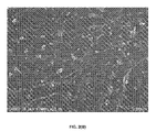
- FIG. 2B is a scanning electron microscope photograph showing a transparent conductive polycarbonate film according to an embodiment of the present invention.
- the present invention provides a transparent conductive polycarbonate film provided thereon with a transparent conductive layer by coating a transparent polycarbonate with a one-component mixed solution of carbon nanotubes and a binder on one side or both sides thereof.
- the transparent conductive polycarbonate film must have a surface resistance of 10 3 ⁇ /sq or less and a transmissivity of 70% or more in a wavelength of 540 ⁇ 560 nm, and can be used as an electrode of various transparent displays.
- the transparent conductive polycarbonate film is prepared by directly forming a transparent conductive layer composed of nanotubes on a polycarbonate film used as a protective film of a liquid crystal display in a conventional touch panel, a touch panel having higher transmissivity than a conventional touch panel can be manufactured, a thin touch panel can be manufactured, and the production cost of the touch panel can be decreased without using a polyethylene terephthalate (PET) substrate coated with ITO used in order to improve the adhesion between the ITO and the conventional polycarbonate film.
- PET polyethylene terephthalate
- FIG. 1A is a schematic sectional view showing a conventional touch panel
- FIG. 1B is a schematic sectional view showing a touch panel according to an embodiment of the present invention.
- the conventional touch panel includes a protective layer 20 for protecting a liquid crystal display screen 10 ; a transparent conductive film formed on the protective layer 20 , the transparent conductive film including a lower transparent electrode 30 , an upper transparent electrode 40 , and a spacer 50 interposed therebetween; and an external protective layer 60 .
- FIG. 1B a transparent conductive layer 200 composed of carbon nanotubes, which is formed on a polycarbonate film 100 , is used as the lower transparent electrode 30 .
- the upper transparent electrode 40 of the conventional touch panel may be directly used in the touch panel of the present invention.
- FIG. 2A is a photograph showing a transparent conductive polycarbonate film including a transparent conductive layer composed of carbon nanotubes according to an embodiment of the present invention
- FIG. 2B is a scanning electron microscope photograph showing a transparent conductive polycarbonate film according to an embodiment of the present invention.
- a transparent conductive polycarbonate film on which a mono-layered transparent conductive layer having a predetermined amount of a binder is formed may be manufactured, or a transparent conductive polycarbonate film on which a multi-layered transparent conductive layer is formed may be manufactured by sequentially coating a polycarbonate film with a plurality of mixed solutions of carbon nanotubes and a binder depending on the function and use of the conductive polycarbonate film.
- the mono-layered transparent conductive layer may simultaneously serve as a conductive layer, a protective layer and an adhesive layer.
- the amount of a binder included in the mono-layered transparent conductive layer be 10 ⁇ 99.9 parts by weight based on 100 parts by weight of a mixture of carbon nanotubes and a binder.
- the multi-layered transparent conductive layer must include a conductive layer in order to ensure conductivity, and a protective layer or an adhesive layer must be formed on or beneath the conductive layer.
- These conductive, protective and adhesive layers are formed by preparing a mixed solution of nanotubes and a binder depending on the amount of the binder and then applying the mixed solution onto a polycarbonate film.
- the protective layer formed on the conductive layer serves to prevent the scattering of nanoparticles including nanotubes constituting the conductive layer and to improve the chemical resistance, moisture resistance and scratch resistance of a transparent conductive polycarbonate film.
- the adhesive layer which is formed beneath the conductive layer, that is, on the polycarbonate film, serves to maintain the adhesion between the conductive layer and polycarbonate film and thus to improve the durability of the transparent conductive polycarbonate film, that is, the durability thereof against a touch pen at the time of use of a touch panel.
- These conductive, protective and adhesive layers may be formed into two layers including a conductive layer and a protective layer or a conductive layer and an adhesive layer, or may be formed into three layers including a conductive layer, a protective layer and an adhesive layer. If necessary, these layers may be repeatedly formed regularly or irregularly.
- the conductivity of these conductive layers, protective layers and adhesive layers generally decreases with the increase in the amount of a binder, the amount of the binder in the conductive layer is lower than the amount of the binder in the protective layer or adhesive layer.
- the transparent conductive layer formed on the polycarbonate film includes three layers, that is, when an adhesive layer, conductive layer and a protective layer are formed on the polycarbonate film, it is preferred that the amount of a binder included in the adhesive layer be 20 ⁇ 99.9 parts by weight based on 100 parts by weight of a mixture of carbon nanotubes and a binder, the amount of a binder included in the conductive layer be 0.1 ⁇ 50 parts by weight based on 100 parts by weight of a mixture of carbon nanotubes and a binder, and the amount of a binder included in the protective layer be 20 ⁇ 99.9 parts by weight based on 100 parts by weight of a mixture of carbon nanotubes and a binder.
- the transparent conductive layer when the amount of the adhesive layer or protective layer is higher that that of the conductive layer, durability against a touch pen as well as electrical conductivity must be ensured.
- the transparent conductive layer when the transparent conductive layer includes three layers, the transparent conductive layer is configured such that the maximum amount of a binder included in the conductive layer is 50 parts by weight based on 100 parts by weight of a mixture of carbon nanotubes and a binder, and thus conductivity is relatively increased.
- each of them exhibit conductivity, the adhesivity of the portion thereof to which the polycarbonate film is adhered is improved, and the surface of the conductive layer is treated such that the protective function for preventing the scattering of nanoparticles is improved, thereby entirely making up for the function of the conductive layer.
- the transparent conductive layer formed on the polycarbonate film includes two layers
- the transparent conductive layer includes an adhesive layer formed on the polycarbonate film and a conduction-protection mixed layer for simultaneously performing functions of a conductive layer and a protective layer formed on the adhesive layer, or includes a conduction-adhesion mixed layer formed on the polycarbonate film and a protective layer formed on the conduction-adhesion mixed layer.
- the transparent conductive layer includes the adhesive layer and conduction-protection mixed layer
- the amount of a binder included in the adhesive layer be 20 ⁇ 99.9 parts by weight based on 100 parts by weight of a mixture of carbon nanotubes and a binder
- the amount of a binder included in the conduction-protection mixed layer be 0.1 ⁇ 70 parts by weight based on 100 parts by weight of a mixture of carbon nanotubes and a binder.
- the transparent conductive layer basically has conductivity.
- the transparent conductive layer is configured such that the maximum amount of a binder included in the adhesive layer is 99.9 parts by weight based on 100 parts by weight of a mixture of carbon nanotubes and a binder, so that the adhesion between the conductive layer and polycarbonate film is improved, thereby a transparent conductive polycarbonate film including the transparent conductive layer can be used in the fields of requiring durability.
- the transparent conductive layer includes the conduction-adhesion mixed layer and protective layer
- the amount of a binder included in the conduction-adhesion mixed layer be 0.1 ⁇ 70 parts by weight based on 100 parts by weight of a mixture of carbon nanotubes and a binder
- the amount of a binder included in the protective layer be 20 ⁇ 99.9 parts by weight based on 100 parts by weight of a mixture of carbon nanotubes and a binder.
- the transparent conductive layer basically has conductivity.
- the transparent conductive layer is configured such that the maximum amount of a binder included in the conduction-adhesion mixed layer is 70 parts by weight based on 100 parts by weight of a mixture of carbon nanotubes and a binder and the minimum amount of a binder included in the protective layer is 20 parts by weight based on 100 parts by weight of a mixture of carbon nanotubes and a binder, so that the hybrid function between the conductive layer and adhesive layer can be performed and the protective layer having a high binder content prevent the scattering of nanoparticles, thereby a transparent conductive polycarbonate film including the transparent conductive layer can be used in the fields of requiring chemical resistance, moisture resistance and scratch resistance.
- the function of the protective layer can be improved and the function of the adhesive layer can be more improved while the function of the conductive layer being basically maintained, depending on the use of a transparent conductive polycarbonate film.
- carbon nanotubes may be selected from among single-wall carbon nanotubes, double-wall carbon nanotubes and multi-wall carbon nanotubes.
- carbon nanotubes relatively cheap carbon nanotubes having an outer diameter of less than 15 nm may be used. From this, unlike where only carbon nanotubes having an outer diameter of less than 3 nm can be used in conventional technologies, it can be seen that carbon nanotubes having a larger outer diameter can also be used through the improvement of dispersibility.
- multi-wall nanotubes since their refractive indices are changed due to the increase in thickness of multi-walls and their transmissivity is deteriorated due to Rayleigh scattering, multi-wall nanotubes having a particle size of less than wavelength ( ⁇ )/20 must be used in consideration of the dispersion of particles, etc.
- carbon nanotubes having an outer diameter of less than 15 nm can be used in the visible region.
- the reason for this is that the dispersibility of carbon nanotubes is improved by the solvent and binder according to the present invention.
- the carbon nanotubes are dissolved in a solvent.
- the solvent may be a polar solvent or a nonpolar solvent, and may be one or more selected from the group consisting of acetone, methylethyl ketone, methyl alcohol, ethyl alcohol, isopropyl alcohol, butyl alcohol, ethylene glycol, polyethylene glycol, tetrahydrofuran, dimethylformamide, dimethylacetamide, N-methyl-2-pyrrolidone, hexane, cyclohexanone, toluene, chloroform, distilled water, dichlorobenzene, dimethylbenzene, trimethylbenzene, pyridine, methylnaphthalene, nitromethane, acrylonitrile, octadecylamine, aniline, dimethylsulfoxide.
- the selected one or more solvents are prepared into a carbon nanotube-dispersed solution.
- an ultrasonic dispersion method or a ball milling method is used. That is, carbon nanotubes are uniformly dispersed in the solvent by applying them in an ultrasonic dispersion apparatus having a frequency of 20 ⁇ 50 kHz and a power of 50 ⁇ 700 W for 1 ⁇ 60 hours.
- a dispersion stabilizer is added thereto, so that the dispersity of the carbon nanotubes into the solvent is further improved, with the result that the finally produced transparent conductive polycarbonate film can be maintained in a stable state without changing the physical properties thereof, thereby providing a transparent conductive polycarbonate film having uniform properties.
- the acid may be selected from among nitric acid, chloric acid, sulfuric acid and a mixture thereof, and thus carboxylic groups are introduced into the end and surface of the carbon nanotubes. That is, carbon nanotubes are washed with distilled water and simultaneously residual acid is removed therefrom, and then the carbon nanotubes are filtered and dried, thereby obtaining refined carbon nanotubes substituted with carboxylic groups. These refined carbon nanotubes are dispersed in the solvent to prepare a carbon nanotube-dispersed solution, and then a binder is added to the carbon nanotube-dispersed solution.
- a mixed solution of carbon nanotubes and a binder may be prepared by mixing a binder with the carbon nanotube-dispersed solution at the time of preparing the carbon nanotube-dispersed solution or by additionally preparing a binder solution in which a binder is mixed with a polar or nonpolar solvent and then mixing the binder solution with the carbon nanotube-dispersed solution.
- the amount of a binder is suitably determined in the above range in consideration of the use, transparency and electrical conductivity of a transparent conductive polycarbonate film, and a plurality of mixed solutions of carbon nanotubes and a binder is prepared.
- the amount of a binder is an important factor for determining the adhesivity to polycarbonate film, electrical conductivity, transmissivity, dispersibility, chemical stability, durability and scratch resistance.
- the amount of a binder is increased, the adhesivity to polycarbonate film, dispersibility, chemical stability, durability and scratch resistance are increased, but the electrical conductivity and transmissivity are decreased.
- the mixed solution of carbon nanotubes and a binder is prepared by selecting the optimal amount of a binder.
- the binder may be selected from among thermoplastic resins, thermosetting resins, photo-curable resins, silane compounds, titanium compounds, copolymers, self-assembled resins, conductive polymers, and combinations thereof.
- the binder serves to improve the dispersibility of carbon nanotubes, improve the adhesivity to a polycarbonate film, and improve chemical stability, durability and scratch resistance.
- a method of coating a polycarbonate film with the mixed solution of carbon nanotubes and a binder may be performed by any one method selected from among spraying, dip coating, spin coating, screen coating, ink-jet printing, pad printing, knife coating, kiss coating, and gravure coating.
- the viscosity of the mixed solution of carbon nanotubes and a binder is controlled through the addition of a solvent or reduced-pressure distillation depending on each of the coating methods, and then the viscosity-controlled mixed solution of carbon nanotubes and a binder may be applied on the polycarbonate film.
- the polycarbonate film is coated thereon with the mixed solution of carbon nanotubes and a binder such that the thickness thereof is several tens to several hundreds of nanometers. Subsequently, a solvent drying process and a process of curing a binder are performed, thus completing a transparent conductive film of the present invention.
- the solvent drying process and the process of curing the binder may be formed during the formation of a multi-layered transparent conductive layer, or may be formed after the completion of the entire multi-layered transparent conductive layer.
- the present invention provides a transparent conductive polycarbonate film coated with a mixed solution of carbon nanotubes and a binder, by which a touch panel having high transmissivity can be manufactured by directly forming a transparent conductive layer on a polycarbonate film used as a protective film of a liquid crystal display using carbon nanotubes, without using a polyethylene terephthalate (PET) substrate used for a transparent electrode of a conventional touch panel, by which the production cost of the touch panel can be decreased, and by which a thin touch panel can be manufactured.
- PET polyethylene terephthalate
Abstract
Description
- The present invention relates to a transparent conductive polycarbonate film coated with carbon nanotubes and a touch panel using the same, and, more particularly, to a transparent conductive polycarbonate film coated with carbon nanotubes, by which a touch panel having high transmissivity can be manufactured through simple processes, without using a conventional polyethylene terephthalate (PET) substrate coated with indium tin oxide (ITO), and a touch panel using the same.
- Generally, a transparent conductive film must have high conductivity (surface resistance of 1×10³ Ω/sq or less) and high transmissivity in a visible region. Such a transparent conductive film is used to manufacture plasma display panels (PDPs), liquid crystal displays (LCDs), light emitting diodes (LEDs), organic light emitting displays (OLEDs), touch panels, solar cells, and the like.
- Particularly, in the present invention, a transparent conductive film used to manufacture a touch panel will be described.
- Generally, a touch panel is an apparatus for recognizing input signals generated by touching letters or figures displayed on a liquid crystal display screen with hands or touch pens without using additional input devices, such as keyboards, mousse, and the like.
- Such a touch panel, as shown in
FIG. 1A , includes: a liquid crystal display (LCD)screen 10; aprotective layer 20 formed on the liquid crystal display (LCD)screen 10 to protect the liquid crystal display (LCD)screen 10; a transparent conductive film formed on theprotective layer 20, the transparent conductive film including a lowertransparent electrode 30, an uppertransparent electrode 40, and aspacer 50 interposed therebetween; and an externalprotective layer 60 made of polymethylmethacrylate (PMMA), the external protective layer being formed by a hard coating method. - The
protective layer 20 for protecting the liquidcrystal display screen 10 is generally made of polycarbonate, and the lowertransparent electrode 30 and uppertransparent electrode 40, which constitute a transparent conductive film, must function as electrodes and simultaneously have a transmissivity of 70% or more in a visible region. - Conventionally, an indium tin oxide (hereinafter, referred to as ‘ITO’) electrode is most widely used to manufacture the transparent electrode. The ITO is advantageous in that it has excellent physical properties and has been frequently used in a process of manufacturing a transparent electrode to date, but is problematic in that, since indium oxide (In2O3) is obtainable from a zinc (Zn) mine just as a by-product, the supply and demand thereof is unstable. Further, ITO film is problematic in that since the ITO film does not have flexibility, it cannot be used for flexible products, and further in that since the ITO film is manufactured under high temperature and high pressure conditions, the production cost thereof is increased.
- Further, when the protective layer formed on the liquid crystal display is coated with the ITO in order to be used as the transparent electrode of the touch panel, the most important problem is the adhesion between the ITO and the polycarbonate constituting the protective layer. Generally, since the adhesion between the ITO and polycarbonate is not high, a polyethylene terephthalate (PET) substrate is coated with ITO, and then adhered on the protective layer made of polycarbonate.
- However, this method is problematic in that the transmissivity of the liquid crystal display screen is decreased, and in that a process of coating a polyethylene terephthalate (PET) substrate with ITO is additionally conducted, so that costs are increased, thereby increasing the thickness of the touch panel.
- Accordingly, the present invention has been made keeping in mind the above problems occurring in the prior art, and an object of the present invention is to provide a transparent conductive polycarbonate film coated on one side or both sides thereof with a mixed solution of carbon nanotubes and a binder, by which a touch panel having high transmissivity can be manufactured by directly forming a transparent conductive layer on a polycarbonate film used as the protective film of a liquid crystal display using carbon nanotubes, without using a polyethylene terephthalate (PET) substrate used for a transparent electrode of a conventional touch panel, by which the production cost of the touch panel can be decreased, and by which a thin touch panel can be manufactured.
- In order to accomplish the above object, the present invention provides a transparent conductive polycarbonate film coated with carbon nanotubes, including a transparent conductive layer formed by applying a mixed solution of carbon nanotubes and a binder on one side or both sides of a transparent polycarbonate film, and a touch panel using the transparent conductive polycarbonate film as a lower electrode.
- Further, it is preferred that the carbon nanotubes be selected from among single-wall carbon nanotubes, double-wall carbon nanotubes, multi-wall carbon nanotubes, and mixtures thereof.
- Further, it preferred that the transparent conductive polycarbonate film have a surface resistance of 1×10³Ω/sq or less and a transmissivity of 70% or more in a wavelength of 540˜560 nm.
- Further, it preferred that, in the coating of the mixed solution of carbon nanotubes and a binder, the transparent conductive polycarbonate film be provided on one side or both sides thereof with a mono-layered transparent conductive layer having a predetermined amount of a binder or a multi-layered transparent conductive layer having different amounts of a binder.
- Further, it is preferred that the multi-layered transparent conductive layer include a conductive layer; and a protective layer formed on the conductive layer or an adhesive layer beneath the conductive layer.
- Further, it is preferred that the conductive layer have a lower binder content than that of the adhesive layer or the protective layer.
- Further, it is preferred that the multi-layered transparent conductive layer include an adhesive layer formed on the polycarbonate film; a conductive layer formed on the adhesive layer; and a protective layer formed on the conductive layer. Further, it is preferred that the amount of a binder included in the adhesive layer be 20˜99.9 parts by weight based on 100 parts by weight of a mixture of carbon nanotubes and a binder, that the amount of a binder included in the conductive layer be 0.1˜50 parts by weight based on 100 parts by weight of a mixture of carbon nanotubes and a binder, and that the amount of a binder included in the protective layer be 20˜99.9 parts by weight based on 100 parts by weight of a mixture of carbon nanotubes and a binder.
- Further, it is preferred that the multi-layered transparent conductive layer include an adhesive layer formed on the polycarbonate film; and a conduction-protection mixed layer, serving as both a conductive layer and a protective layer, formed on the adhesive layer. Further, it is preferred that the amount of a binder included in the adhesive layer be 20˜99.9 parts by weight based on 100 parts by weight of a mixture of carbon nanotubes and a binder, and the amount of a binder included in the conduction-protection mixed layer be 0.1˜70 parts by weight based on 100 parts by weight of a mixture of carbon nanotubes and a binder.
- Further, it is preferred that the multi-layered transparent conductive layer include a conduction-adhesion mixed layer, serving as both a conductive layer and an adhesive layer, formed on the polycarbonate film, and a protective layer formed on the conduction-adhesion mixed layer. Further, it is preferred that the amount of a binder included in the conduction-adhesion mixed layer be 0.1˜70 parts by weight based on 100 parts by weight of a mixture of carbon nanotubes and a binder, and the amount of a binder included in the protective layer be 20˜99.9 parts by weight based on 100 parts by weight of a mixture of carbon nanotubes and a binder.
- Here, it is preferred that the binder be selected from among thermoplastic resins, thermosetting resins, photo-curable resins, silane compounds, titanium compounds, copolymers, self-assembled resins, conductive polymers, and combinations thereof.
- Further, it is preferred that the carbon nanotube have an outer diameter of 0.5˜15 nm.
- The above and other objects, features and advantages of the present invention will be more clearly understood from the following detailed description taken in conjunction with the accompanying drawings, in which:
-
FIG. 1A is a schematic sectional view showing a conventional touch panel; -
FIG. 1B is a schematic sectional view showing a touch panel according to an embodiment of the present invention; -
FIG. 2A is a photograph showing a transparent conductive polycarbonate film including a transparent conductive layer composed of carbon nanotubes, having a thickness of 1 mm, according to an embodiment of the present invention; and -
FIG. 2B is a scanning electron microscope photograph showing a transparent conductive polycarbonate film according to an embodiment of the present invention. - Hereinafter, preferred embodiments of the present invention will be described in detail with reference to the attached drawings.
- The present invention provides a transparent conductive polycarbonate film provided thereon with a transparent conductive layer by coating a transparent polycarbonate with a one-component mixed solution of carbon nanotubes and a binder on one side or both sides thereof.
- The transparent conductive polycarbonate film must have a surface resistance of 103 Ω/sq or less and a transmissivity of 70% or more in a wavelength of 540˜560 nm, and can be used as an electrode of various transparent displays.
- Particularly, since the transparent conductive polycarbonate film is prepared by directly forming a transparent conductive layer composed of nanotubes on a polycarbonate film used as a protective film of a liquid crystal display in a conventional touch panel, a touch panel having higher transmissivity than a conventional touch panel can be manufactured, a thin touch panel can be manufactured, and the production cost of the touch panel can be decreased without using a polyethylene terephthalate (PET) substrate coated with ITO used in order to improve the adhesion between the ITO and the conventional polycarbonate film.
-
FIG. 1A is a schematic sectional view showing a conventional touch panel, andFIG. 1B is a schematic sectional view showing a touch panel according to an embodiment of the present invention. As shown inFIG. 1A , the conventional touch panel includes aprotective layer 20 for protecting a liquidcrystal display screen 10; a transparent conductive film formed on theprotective layer 20, the transparent conductive film including a lowertransparent electrode 30, an uppertransparent electrode 40, and aspacer 50 interposed therebetween; and an externalprotective layer 60. - In the conventional touch panel, a polyethylene terephthalate (PET) film coated with ITO, which is formed on a
polycarbonate film 20, is used as the lowertransparent electrode 30. In contrast, according to the touch panel of the present invention, as shown inFIG. 1B , a transparentconductive layer 200 composed of carbon nanotubes, which is formed on apolycarbonate film 100, is used as the lowertransparent electrode 30. Here, the uppertransparent electrode 40 of the conventional touch panel may be directly used in the touch panel of the present invention.FIG. 2A is a photograph showing a transparent conductive polycarbonate film including a transparent conductive layer composed of carbon nanotubes according to an embodiment of the present invention, andFIG. 2B is a scanning electron microscope photograph showing a transparent conductive polycarbonate film according to an embodiment of the present invention. - In the present invention, a transparent conductive polycarbonate film on which a mono-layered transparent conductive layer having a predetermined amount of a binder is formed may be manufactured, or a transparent conductive polycarbonate film on which a multi-layered transparent conductive layer is formed may be manufactured by sequentially coating a polycarbonate film with a plurality of mixed solutions of carbon nanotubes and a binder depending on the function and use of the conductive polycarbonate film.
- The mono-layered transparent conductive layer may simultaneously serve as a conductive layer, a protective layer and an adhesive layer. In this case, it is preferred that the amount of a binder included in the mono-layered transparent conductive layer be 10˜99.9 parts by weight based on 100 parts by weight of a mixture of carbon nanotubes and a binder.
- The multi-layered transparent conductive layer must include a conductive layer in order to ensure conductivity, and a protective layer or an adhesive layer must be formed on or beneath the conductive layer. These conductive, protective and adhesive layers are formed by preparing a mixed solution of nanotubes and a binder depending on the amount of the binder and then applying the mixed solution onto a polycarbonate film.
- The protective layer formed on the conductive layer serves to prevent the scattering of nanoparticles including nanotubes constituting the conductive layer and to improve the chemical resistance, moisture resistance and scratch resistance of a transparent conductive polycarbonate film.
- The adhesive layer which is formed beneath the conductive layer, that is, on the polycarbonate film, serves to maintain the adhesion between the conductive layer and polycarbonate film and thus to improve the durability of the transparent conductive polycarbonate film, that is, the durability thereof against a touch pen at the time of use of a touch panel.
- These conductive, protective and adhesive layers, if necessary, may be formed into two layers including a conductive layer and a protective layer or a conductive layer and an adhesive layer, or may be formed into three layers including a conductive layer, a protective layer and an adhesive layer. If necessary, these layers may be repeatedly formed regularly or irregularly.
- Considering that the conductivity of these conductive layers, protective layers and adhesive layers generally decreases with the increase in the amount of a binder, the amount of the binder in the conductive layer is lower than the amount of the binder in the protective layer or adhesive layer.
- When the transparent conductive layer formed on the polycarbonate film includes three layers, that is, when an adhesive layer, conductive layer and a protective layer are formed on the polycarbonate film, it is preferred that the amount of a binder included in the adhesive layer be 20 ˜99.9 parts by weight based on 100 parts by weight of a mixture of carbon nanotubes and a binder, the amount of a binder included in the conductive layer be 0.1˜50 parts by weight based on 100 parts by weight of a mixture of carbon nanotubes and a binder, and the amount of a binder included in the protective layer be 20˜99.9 parts by weight based on 100 parts by weight of a mixture of carbon nanotubes and a binder.
- When the amount of the adhesive layer or protective layer is higher that that of the conductive layer, durability against a touch pen as well as electrical conductivity must be ensured. As described above, when the transparent conductive layer includes three layers, the transparent conductive layer is configured such that the maximum amount of a binder included in the conductive layer is 50 parts by weight based on 100 parts by weight of a mixture of carbon nanotubes and a binder, and thus conductivity is relatively increased.
- That is, basically, in the adhesive layer, conductive layer and protective layer formed on a polycarbonate film, each of them exhibit conductivity, the adhesivity of the portion thereof to which the polycarbonate film is adhered is improved, and the surface of the conductive layer is treated such that the protective function for preventing the scattering of nanoparticles is improved, thereby entirely making up for the function of the conductive layer.
- Meanwhile, when the transparent conductive layer formed on the polycarbonate film includes two layers, the transparent conductive layer includes an adhesive layer formed on the polycarbonate film and a conduction-protection mixed layer for simultaneously performing functions of a conductive layer and a protective layer formed on the adhesive layer, or includes a conduction-adhesion mixed layer formed on the polycarbonate film and a protective layer formed on the conduction-adhesion mixed layer.
- When the transparent conductive layer includes the adhesive layer and conduction-protection mixed layer, it is preferred that the amount of a binder included in the adhesive layer be 20˜99.9 parts by weight based on 100 parts by weight of a mixture of carbon nanotubes and a binder, and the amount of a binder included in the conduction-protection mixed layer be 0.1˜70 parts by weight based on 100 parts by weight of a mixture of carbon nanotubes and a binder.
- Even when the transparent conductive layer includes the adhesive layer and conduction-protection mixed layer, the transparent conductive layer basically has conductivity. In this case, the transparent conductive layer is configured such that the maximum amount of a binder included in the adhesive layer is 99.9 parts by weight based on 100 parts by weight of a mixture of carbon nanotubes and a binder, so that the adhesion between the conductive layer and polycarbonate film is improved, thereby a transparent conductive polycarbonate film including the transparent conductive layer can be used in the fields of requiring durability.
- When the transparent conductive layer includes the conduction-adhesion mixed layer and protective layer, it is preferred that the amount of a binder included in the conduction-adhesion mixed layer be 0.1˜70 parts by weight based on 100 parts by weight of a mixture of carbon nanotubes and a binder, and the amount of a binder included in the protective layer be 20˜99.9 parts by weight based on 100 parts by weight of a mixture of carbon nanotubes and a binder.
- Even when the transparent conductive layer includes the conduction-adhesion mixed layer and protective layer, the transparent conductive layer basically has conductivity. In this case, the transparent conductive layer is configured such that the maximum amount of a binder included in the conduction-adhesion mixed layer is 70 parts by weight based on 100 parts by weight of a mixture of carbon nanotubes and a binder and the minimum amount of a binder included in the protective layer is 20 parts by weight based on 100 parts by weight of a mixture of carbon nanotubes and a binder, so that the hybrid function between the conductive layer and adhesive layer can be performed and the protective layer having a high binder content prevent the scattering of nanoparticles, thereby a transparent conductive polycarbonate film including the transparent conductive layer can be used in the fields of requiring chemical resistance, moisture resistance and scratch resistance.
- As described above, since the multi-layered transparent conductive layer is formed depending on the amount of binder, the function of the protective layer can be improved and the function of the adhesive layer can be more improved while the function of the conductive layer being basically maintained, depending on the use of a transparent conductive polycarbonate film.
- Here, carbon nanotubes may be selected from among single-wall carbon nanotubes, double-wall carbon nanotubes and multi-wall carbon nanotubes.
- As the carbon nanotubes, relatively cheap carbon nanotubes having an outer diameter of less than 15 nm may be used. From this, unlike where only carbon nanotubes having an outer diameter of less than 3 nm can be used in conventional technologies, it can be seen that carbon nanotubes having a larger outer diameter can also be used through the improvement of dispersibility. In the case of multi-wall nanotubes, since their refractive indices are changed due to the increase in thickness of multi-walls and their transmissivity is deteriorated due to Rayleigh scattering, multi-wall nanotubes having a particle size of less than wavelength (λ)/20 must be used in consideration of the dispersion of particles, etc. Considering the transparency of film and the dispersibility of carbon nanotubes, carbon nanotubes having an outer diameter of less than 15 nm (d<λ/20d<˜15 nm) can be used in the visible region. The reason for this is that the dispersibility of carbon nanotubes is improved by the solvent and binder according to the present invention.

- In order to primarily disperse carbon nanotubes, the carbon nanotubes are dissolved in a solvent. Here, the solvent may be a polar solvent or a nonpolar solvent, and may be one or more selected from the group consisting of acetone, methylethyl ketone, methyl alcohol, ethyl alcohol, isopropyl alcohol, butyl alcohol, ethylene glycol, polyethylene glycol, tetrahydrofuran, dimethylformamide, dimethylacetamide, N-methyl-2-pyrrolidone, hexane, cyclohexanone, toluene, chloroform, distilled water, dichlorobenzene, dimethylbenzene, trimethylbenzene, pyridine, methylnaphthalene, nitromethane, acrylonitrile, octadecylamine, aniline, dimethylsulfoxide. The selected one or more solvents are prepared into a carbon nanotube-dispersed solution.
- Further, in order to disperse carbon nanotubes in the solvent, an ultrasonic dispersion method or a ball milling method is used. That is, carbon nanotubes are uniformly dispersed in the solvent by applying them in an ultrasonic dispersion apparatus having a frequency of 20˜50 kHz and a power of 50˜700 W for 1˜60 hours.
- Further, when carbon nanotubes are dispersed in the solvent, a dispersion stabilizer is added thereto, so that the dispersity of the carbon nanotubes into the solvent is further improved, with the result that the finally produced transparent conductive polycarbonate film can be maintained in a stable state without changing the physical properties thereof, thereby providing a transparent conductive polycarbonate film having uniform properties.
- Here, before the carbon nanotube-dispersed solution is prepared, in order to ensure the dispersibility and dispersion stability of carbon nanotubes into a solvent and a binder, surface functionalization through acid treatment may be performed. In the acid treatment, the acid may be selected from among nitric acid, chloric acid, sulfuric acid and a mixture thereof, and thus carboxylic groups are introduced into the end and surface of the carbon nanotubes. That is, carbon nanotubes are washed with distilled water and simultaneously residual acid is removed therefrom, and then the carbon nanotubes are filtered and dried, thereby obtaining refined carbon nanotubes substituted with carboxylic groups. These refined carbon nanotubes are dispersed in the solvent to prepare a carbon nanotube-dispersed solution, and then a binder is added to the carbon nanotube-dispersed solution.
- A mixed solution of carbon nanotubes and a binder may be prepared by mixing a binder with the carbon nanotube-dispersed solution at the time of preparing the carbon nanotube-dispersed solution or by additionally preparing a binder solution in which a binder is mixed with a polar or nonpolar solvent and then mixing the binder solution with the carbon nanotube-dispersed solution. Here, the amount of a binder is suitably determined in the above range in consideration of the use, transparency and electrical conductivity of a transparent conductive polycarbonate film, and a plurality of mixed solutions of carbon nanotubes and a binder is prepared.
- Generally, the amount of a binder is an important factor for determining the adhesivity to polycarbonate film, electrical conductivity, transmissivity, dispersibility, chemical stability, durability and scratch resistance. When the amount of a binder is increased, the adhesivity to polycarbonate film, dispersibility, chemical stability, durability and scratch resistance are increased, but the electrical conductivity and transmissivity are decreased. Considering this, the mixed solution of carbon nanotubes and a binder is prepared by selecting the optimal amount of a binder.
- Here, the binder may be selected from among thermoplastic resins, thermosetting resins, photo-curable resins, silane compounds, titanium compounds, copolymers, self-assembled resins, conductive polymers, and combinations thereof. The binder serves to improve the dispersibility of carbon nanotubes, improve the adhesivity to a polycarbonate film, and improve chemical stability, durability and scratch resistance.
- Here, a method of coating a polycarbonate film with the mixed solution of carbon nanotubes and a binder may be performed by any one method selected from among spraying, dip coating, spin coating, screen coating, ink-jet printing, pad printing, knife coating, kiss coating, and gravure coating. In addition, before the coating process, the viscosity of the mixed solution of carbon nanotubes and a binder is controlled through the addition of a solvent or reduced-pressure distillation depending on each of the coating methods, and then the viscosity-controlled mixed solution of carbon nanotubes and a binder may be applied on the polycarbonate film.
- Through this coating method, the polycarbonate film is coated thereon with the mixed solution of carbon nanotubes and a binder such that the thickness thereof is several tens to several hundreds of nanometers. Subsequently, a solvent drying process and a process of curing a binder are performed, thus completing a transparent conductive film of the present invention.
- Further, the solvent drying process and the process of curing the binder may be formed during the formation of a multi-layered transparent conductive layer, or may be formed after the completion of the entire multi-layered transparent conductive layer.
- As described above, the present invention provides a transparent conductive polycarbonate film coated with a mixed solution of carbon nanotubes and a binder, by which a touch panel having high transmissivity can be manufactured by directly forming a transparent conductive layer on a polycarbonate film used as a protective film of a liquid crystal display using carbon nanotubes, without using a polyethylene terephthalate (PET) substrate used for a transparent electrode of a conventional touch panel, by which the production cost of the touch panel can be decreased, and by which a thin touch panel can be manufactured.
- Although the preferred embodiments of the present invention have been disclosed for illustrative purposes, those skilled in the art will appreciate that various modifications, additions and substitutions are possible, without departing from the scope and spirit of the invention as disclosed in the accompanying claims.
Claims (15)
Applications Claiming Priority (2)
| Application Number | Priority Date | Filing Date | Title |
|---|---|---|---|
| KR10-2008-0080045 | 2008-08-14 | ||
| KR1020080080045A KR101091196B1 (en) | 2008-08-14 | 2008-08-14 | transparent conductive films containing carbon nanotubes and the touch panel |
Publications (2)
| Publication Number | Publication Date |
|---|---|
| US20100040887A1 true US20100040887A1 (en) | 2010-02-18 |
| US8741434B2 US8741434B2 (en) | 2014-06-03 |
Family
ID=40090155
Family Applications (1)
| Application Number | Title | Priority Date | Filing Date |
|---|---|---|---|
| US12/247,005 Expired - Fee Related US8741434B2 (en) | 2008-08-14 | 2008-10-07 | Transparent conductive films containing carbon nanotubes and touch panel |
Country Status (7)
| Country | Link |
|---|---|
| US (1) | US8741434B2 (en) |
| EP (1) | EP2154598B1 (en) |
| JP (1) | JP5191854B2 (en) |
| KR (1) | KR101091196B1 (en) |
| CN (1) | CN101650484B (en) |
| DE (1) | DE08166138T1 (en) |
| TW (1) | TWI446062B (en) |
Cited By (7)
| Publication number | Priority date | Publication date | Assignee | Title |
|---|---|---|---|---|
| US20120015098A1 (en) * | 2010-07-14 | 2012-01-19 | Qian Cheng | Carbon nanotube based transparent conductive films and methods for preparing and patterning the same |
| US20120097434A1 (en) * | 2010-04-28 | 2012-04-26 | Sony Corporation | Electroconductive element, electroconductive element manufacturing method, wiring element, information input device, display device, and electronic apparatus |
| US20120199384A1 (en) * | 2011-02-07 | 2012-08-09 | Sony Corporation | Conduction element, manufacturing method thereof, wiring element, information input device, display device, and electronic apparatus |
| CN104915072A (en) * | 2014-03-13 | 2015-09-16 | 天津富纳源创科技有限公司 | Touch panel and touch type human-machine interaction device with same |
| WO2015156894A3 (en) * | 2014-01-24 | 2016-01-07 | William Marsh Rice University | Carbon nanotube-coated substrates and methods of making the same |
| US9506194B2 (en) | 2012-09-04 | 2016-11-29 | Ocv Intellectual Capital, Llc | Dispersion of carbon enhanced reinforcement fibers in aqueous or non-aqueous media |
| EP2544029B1 (en) * | 2011-04-12 | 2019-12-25 | Kuang-Chi Innovative Technology Ltd. | Artificial dielectric material |
Families Citing this family (17)
| Publication number | Priority date | Publication date | Assignee | Title |
|---|---|---|---|---|
| CN102314244A (en) * | 2010-06-29 | 2012-01-11 | 东莞万士达液晶显示器有限公司 | Touch control display panel |
| KR101082379B1 (en) | 2010-07-05 | 2011-11-10 | 한국과학기술원 | Piezoresistive device, method of manufacturing the same and piezoresistive-type touch panel having the same |
| JP5605373B2 (en) * | 2010-10-29 | 2014-10-15 | 東レ株式会社 | Method for producing carbon nanotube aggregate dispersion |
| GB201019212D0 (en) * | 2010-11-12 | 2010-12-29 | Dupont Teijin Films Us Ltd | Polyester film |
| IT1403200B1 (en) | 2010-12-23 | 2013-10-15 | Gdm Spa | METHOD AND UNIT OF BENDING HYGIENIC ABSORBENTS. |
| KR20130078764A (en) * | 2011-12-30 | 2013-07-10 | 코오롱인더스트리 주식회사 | Transparent conductive film |
| KR101328681B1 (en) * | 2012-02-24 | 2013-11-14 | 하이텍코리아주식회사 | Length Adjustable Having Conductive Type Touch Pen |
| KR101328682B1 (en) * | 2012-02-24 | 2013-11-14 | 하이텍코리아주식회사 | Conductive Type Touch Pen |
| CN103383868B (en) * | 2012-05-04 | 2016-09-07 | 远东新世纪股份有限公司 | Transparent conductive lamination body |
| US9356179B2 (en) | 2012-06-22 | 2016-05-31 | Industrial Technology Research Institute | Display panel integrated with photoelectric device |
| US8981391B2 (en) | 2012-06-22 | 2015-03-17 | Industrial Technology Research Institute | Display panel with high transparency |
| TWI482310B (en) * | 2012-06-22 | 2015-04-21 | Ind Tech Res Inst | Light emitting diode structure, light emitting diode package and method of measuring temperature of light emitting diode structure |
| CN104423668A (en) * | 2013-09-02 | 2015-03-18 | 天津富纳源创科技有限公司 | Touch screen preparation method |
| KR102119603B1 (en) * | 2013-09-06 | 2020-06-08 | 엘지이노텍 주식회사 | Touch window and display with the same |
| US11226519B2 (en) | 2018-07-02 | 2022-01-18 | Lg Chem, Ltd. | Optical modulation element |
| KR102567452B1 (en) | 2018-10-31 | 2023-08-17 | 에스케이마이크로웍스솔루션즈 주식회사 | Transparent conductive film with color |
| WO2021133541A1 (en) | 2019-12-23 | 2021-07-01 | E Ink Corporation | Transferable light-transmissive electrode films for electro-optic devices |
Citations (13)
| Publication number | Priority date | Publication date | Assignee | Title |
|---|---|---|---|---|
| US20050042450A1 (en) * | 2003-07-28 | 2005-02-24 | Tdk Corporation | Electrode and electrochemical element employing the same |
| WO2005104141A1 (en) * | 2004-04-20 | 2005-11-03 | Takiron Co., Ltd. | Touch panel-use transparent conductive molded product and touch panel |
| US20060051579A1 (en) * | 2003-01-20 | 2006-03-09 | Teijin Limited | Carbon nanotube coated with aromatic condensation polymer |
| US20060052509A1 (en) * | 2002-11-01 | 2006-03-09 | Mitsubishi Rayon Co., Ltd. | Composition containing carbon nanotubes having coating thereof and process for producing them |
| US20060105146A1 (en) * | 2004-11-12 | 2006-05-18 | Eastman Kodak Company | Touch screen having spacer dots with channels |
| US20060188723A1 (en) * | 2005-02-22 | 2006-08-24 | Eastman Kodak Company | Coating compositions containing single wall carbon nanotubes |
| US20060274049A1 (en) * | 2005-06-02 | 2006-12-07 | Eastman Kodak Company | Multi-layer conductor with carbon nanotubes |
| US20070158610A1 (en) * | 2006-01-12 | 2007-07-12 | Haiping Hong | Carbon naoparticle-containing hydrophilic nanofluid |
| US20070182457A1 (en) * | 2005-06-30 | 2007-08-09 | Tdk Corporation | Transparent conductor and panel switch |
| US20070231561A1 (en) * | 2006-03-31 | 2007-10-04 | 3M Innovative Properties Company | Optical article having an antistatic layer |
| US20080286559A1 (en) * | 2007-05-18 | 2008-11-20 | Korea Electrotechnology Research Institute | Method of Manufacturing Transparent Conductive Film Containing Carbon Nanotubes And Binder, And Transparent Conductive Film Manufactured Thereby |
| US20090032777A1 (en) * | 2005-06-07 | 2009-02-05 | Kuraray Co., Ltd. | Carbon nanotube dispersion liquid and transparent conductive film using same |
| US20090155460A1 (en) * | 2007-09-18 | 2009-06-18 | Rodney Ruoff | Method and system for improving conductivity and mechanical performance of carbon nanotube nets and related materials |
Family Cites Families (13)
| Publication number | Priority date | Publication date | Assignee | Title |
|---|---|---|---|---|
| JPH0782839B2 (en) * | 1986-11-08 | 1995-09-06 | 旭化成工業株式会社 | Secondary battery negative electrode |
| JP3913208B2 (en) * | 2002-11-01 | 2007-05-09 | 三菱レイヨン株式会社 | Carbon nanotube-containing composition, composite having coating film made thereof, and method for producing them |
| KR100685954B1 (en) * | 2002-12-24 | 2007-02-23 | 엘지.필립스 엘시디 주식회사 | Touch Panel |
| JP3959342B2 (en) | 2002-12-26 | 2007-08-15 | 株式会社プラスチック工学研究所 | Sheet resin laminate for touch panel and touch panel |
| JP2004230690A (en) * | 2003-01-30 | 2004-08-19 | Takiron Co Ltd | Antistatic transparent resin sheet |
| US20050209392A1 (en) * | 2003-12-17 | 2005-09-22 | Jiazhong Luo | Polymer binders for flexible and transparent conductive coatings containing carbon nanotubes |
| JP2006171336A (en) * | 2004-12-15 | 2006-06-29 | Takiron Co Ltd | Transparent electrode member for image display, and the image display device |
| US7593004B2 (en) * | 2005-06-02 | 2009-09-22 | Eastman Kodak Company | Touchscreen with conductive layer comprising carbon nanotubes |
| JP4795780B2 (en) * | 2005-11-14 | 2011-10-19 | タキロン株式会社 | Antistatic resin molding |
| US9365728B2 (en) * | 2006-03-09 | 2016-06-14 | Battelle Memorial Institute | Modified carbon nanotubes and methods of forming carbon nanotubes |
| JP5161446B2 (en) * | 2006-08-22 | 2013-03-13 | 帝人デュポンフィルム株式会社 | Conductive film and touch panel using the film |
| KR100790216B1 (en) * | 2006-10-17 | 2008-01-02 | 삼성전자주식회사 | A transparent cnt electrode using conductive dispersant and preparation method thereof |
| KR100801595B1 (en) * | 2006-11-09 | 2008-02-05 | 제일모직주식회사 | Composition of carbon nano tube and transparent and conductive film |
-
2008
- 2008-08-14 KR KR1020080080045A patent/KR101091196B1/en not_active IP Right Cessation
- 2008-10-02 JP JP2008257389A patent/JP5191854B2/en not_active Expired - Fee Related
- 2008-10-07 TW TW97138476A patent/TWI446062B/en not_active IP Right Cessation
- 2008-10-07 US US12/247,005 patent/US8741434B2/en not_active Expired - Fee Related
- 2008-10-08 EP EP08166138.1A patent/EP2154598B1/en active Active
- 2008-10-08 CN CN2008101674487A patent/CN101650484B/en not_active Expired - Fee Related
- 2008-10-08 DE DE2008166138 patent/DE08166138T1/en active Pending
Patent Citations (14)
| Publication number | Priority date | Publication date | Assignee | Title |
|---|---|---|---|---|
| US20060052509A1 (en) * | 2002-11-01 | 2006-03-09 | Mitsubishi Rayon Co., Ltd. | Composition containing carbon nanotubes having coating thereof and process for producing them |
| US20060051579A1 (en) * | 2003-01-20 | 2006-03-09 | Teijin Limited | Carbon nanotube coated with aromatic condensation polymer |
| US20050042450A1 (en) * | 2003-07-28 | 2005-02-24 | Tdk Corporation | Electrode and electrochemical element employing the same |
| US20080029292A1 (en) * | 2004-04-20 | 2008-02-07 | Ryuji Takayama | Transparent Conductive Formed Article for a Touch Panel and Touch Panel |
| WO2005104141A1 (en) * | 2004-04-20 | 2005-11-03 | Takiron Co., Ltd. | Touch panel-use transparent conductive molded product and touch panel |
| US20060105146A1 (en) * | 2004-11-12 | 2006-05-18 | Eastman Kodak Company | Touch screen having spacer dots with channels |
| US20060188723A1 (en) * | 2005-02-22 | 2006-08-24 | Eastman Kodak Company | Coating compositions containing single wall carbon nanotubes |
| US20060274049A1 (en) * | 2005-06-02 | 2006-12-07 | Eastman Kodak Company | Multi-layer conductor with carbon nanotubes |
| US20090032777A1 (en) * | 2005-06-07 | 2009-02-05 | Kuraray Co., Ltd. | Carbon nanotube dispersion liquid and transparent conductive film using same |
| US20070182457A1 (en) * | 2005-06-30 | 2007-08-09 | Tdk Corporation | Transparent conductor and panel switch |
| US20070158610A1 (en) * | 2006-01-12 | 2007-07-12 | Haiping Hong | Carbon naoparticle-containing hydrophilic nanofluid |
| US20070231561A1 (en) * | 2006-03-31 | 2007-10-04 | 3M Innovative Properties Company | Optical article having an antistatic layer |
| US20080286559A1 (en) * | 2007-05-18 | 2008-11-20 | Korea Electrotechnology Research Institute | Method of Manufacturing Transparent Conductive Film Containing Carbon Nanotubes And Binder, And Transparent Conductive Film Manufactured Thereby |
| US20090155460A1 (en) * | 2007-09-18 | 2009-06-18 | Rodney Ruoff | Method and system for improving conductivity and mechanical performance of carbon nanotube nets and related materials |
Non-Patent Citations (6)
| Title |
|---|
| Cardinal, Fading. Retrieved on Aug 18, 2012. http://www.cardinalcorp.com/wp-content/uploads/pdf/tsb/ig/IG11_05-08.pdf * |
| HyperPhysics - Electromagnetic Spectrum (HyperPhysics). Retrieved on 4/11/2013. http://hyperphysics.phy-astr.gsu.edu/hbase/ems1.html * |
| Nanocyl, Multi-wall Nanotubes (MWNT) (Nanocyl). Retrieved on 4/11/2013. http://www.nanocyl.com/CNT-Expertise-Centre/Carbon-Nanotubes/Multi-wall-Nanotubes * |
| Noguchi et al., Carbon Nanotubes as Fillers - ABSTRACT, Journal of the Society of Rubber Industry, Japan, VOL.78;NO.6;PAGE.205-210(2005). * |
| Omnexus, What is Polycarbonate? Retrieved on Aug 18, 2012. http://www.omnexus.com/tc/polycarbonate/index.aspx * |
| Takayama et al., WO2005-104141 machine translation, November 3, 2005. * |
Cited By (10)
| Publication number | Priority date | Publication date | Assignee | Title |
|---|---|---|---|---|
| US20120097434A1 (en) * | 2010-04-28 | 2012-04-26 | Sony Corporation | Electroconductive element, electroconductive element manufacturing method, wiring element, information input device, display device, and electronic apparatus |
| US8928106B2 (en) * | 2010-04-28 | 2015-01-06 | Sony Corporation | Electroconductive element, electroconductive element manufacturing method, wiring element, information input device, display device, and electronic apparatus |
| US20120015098A1 (en) * | 2010-07-14 | 2012-01-19 | Qian Cheng | Carbon nanotube based transparent conductive films and methods for preparing and patterning the same |
| CN102337054A (en) * | 2010-07-14 | 2012-02-01 | 辛泰克公司 | Carbon nanotube based transparent conductive films and methods for preparing and patterning the same |
| US20120199384A1 (en) * | 2011-02-07 | 2012-08-09 | Sony Corporation | Conduction element, manufacturing method thereof, wiring element, information input device, display device, and electronic apparatus |
| US8742530B2 (en) * | 2011-02-07 | 2014-06-03 | Sony Corporation | Conduction element, manufacturing method thereof, wiring element, information input device, display device, and electronic apparatus |
| EP2544029B1 (en) * | 2011-04-12 | 2019-12-25 | Kuang-Chi Innovative Technology Ltd. | Artificial dielectric material |
| US9506194B2 (en) | 2012-09-04 | 2016-11-29 | Ocv Intellectual Capital, Llc | Dispersion of carbon enhanced reinforcement fibers in aqueous or non-aqueous media |
| WO2015156894A3 (en) * | 2014-01-24 | 2016-01-07 | William Marsh Rice University | Carbon nanotube-coated substrates and methods of making the same |
| CN104915072A (en) * | 2014-03-13 | 2015-09-16 | 天津富纳源创科技有限公司 | Touch panel and touch type human-machine interaction device with same |
Also Published As
| Publication number | Publication date |
|---|---|
| DE08166138T1 (en) | 2010-10-21 |
| CN101650484B (en) | 2011-11-16 |
| EP2154598A2 (en) | 2010-02-17 |
| TWI446062B (en) | 2014-07-21 |
| US8741434B2 (en) | 2014-06-03 |
| EP2154598A3 (en) | 2013-07-24 |
| EP2154598B1 (en) | 2018-11-28 |
| KR101091196B1 (en) | 2011-12-09 |
| JP2010043237A (en) | 2010-02-25 |
| KR20100021237A (en) | 2010-02-24 |
| JP5191854B2 (en) | 2013-05-08 |
| TW201007258A (en) | 2010-02-16 |
| CN101650484A (en) | 2010-02-17 |
Similar Documents
| Publication | Publication Date | Title |
|---|---|---|
| US8741434B2 (en) | Transparent conductive films containing carbon nanotubes and touch panel | |
| US8637122B2 (en) | Method of manufacturing transparent conductive film containing carbon nanotubes and binder, and transparent conductive film manufactured thereby | |
| US8237680B2 (en) | Touch panel | |
| US8455043B2 (en) | Method of making transparent conductive film | |
| KR20160117396A (en) | Conductive Paint Composition and the Method of Conductive Film Using Thereof | |
| KR20100088155A (en) | Method for producing carbon nanotube-containing conductor | |
| US20140158411A1 (en) | Substrate having transparent electrode for flexible display and method of fabricating the same | |
| WO2007086878A2 (en) | Coating compositions containing single wall carbon nanotubes | |
| Sloma et al. | Electroluminescent structures printed on paper and textile elastic substrates | |
| JP2015504384A (en) | Base film for manufacturing transparent electrode film | |
| KR101912036B1 (en) | Transparent Electrode and Manufacturing Method Thereof | |
| US20110083886A1 (en) | Method of manufacturing electrode substrate | |
| WO2015075876A1 (en) | Transparent conductor and method for producing transparent conductor | |
| KR101321097B1 (en) | Carbon nano tube transparent electrode, method for manufacturing the same, and coating composition for carbon nano tube transparent electrode | |
| KR100960858B1 (en) | Fabrication method of transparent conductive films containing carbon nanotubes and polymer binders and the transparent conductive films | |
| JP4784550B2 (en) | Transparent conductive paint and transparent conductive film | |
| WO2016129270A1 (en) | Electrode, method for producing same, and touch panel and organic el lighting element each provided with said electrode | |
| JP2011029038A (en) | Method of manufacturing base material with transparent conductive film | |
| WO2016038819A1 (en) | Electrode, method for manufacturing same, and organic el lighting device provided with electrode | |
| TWM517898U (en) | Optical composite layer structure |
Legal Events
| Date | Code | Title | Description |
|---|---|---|---|
| AS | Assignment |
Owner name: KOREA ELECTROTECHNOLOGY RESEARCH INSTITUTE,KOREA, Free format text: ASSIGNMENT OF ASSIGNORS INTEREST;ASSIGNORS:HAN, JOONG TARK;LEE, GEON WOONG;JEONG, HEE JIN;AND OTHERS;REEL/FRAME:021662/0726 Effective date: 20080908 Owner name: KOREA ELECTROTECHNOLOGY RESEARCH INSTITUTE, KOREA, Free format text: ASSIGNMENT OF ASSIGNORS INTEREST;ASSIGNORS:HAN, JOONG TARK;LEE, GEON WOONG;JEONG, HEE JIN;AND OTHERS;REEL/FRAME:021662/0726 Effective date: 20080908 |
|
| STCF | Information on status: patent grant |
Free format text: PATENTED CASE |
|
| MAFP | Maintenance fee payment |
Free format text: PAYMENT OF MAINTENANCE FEE, 4TH YR, SMALL ENTITY (ORIGINAL EVENT CODE: M2551) Year of fee payment: 4 |
|
| FEPP | Fee payment procedure |
Free format text: MAINTENANCE FEE REMINDER MAILED (ORIGINAL EVENT CODE: REM.); ENTITY STATUS OF PATENT OWNER: SMALL ENTITY |
|
| LAPS | Lapse for failure to pay maintenance fees |
Free format text: PATENT EXPIRED FOR FAILURE TO PAY MAINTENANCE FEES (ORIGINAL EVENT CODE: EXP.); ENTITY STATUS OF PATENT OWNER: SMALL ENTITY |
|
| STCH | Information on status: patent discontinuation |
Free format text: PATENT EXPIRED DUE TO NONPAYMENT OF MAINTENANCE FEES UNDER 37 CFR 1.362 |
|
| FP | Lapsed due to failure to pay maintenance fee |
Effective date: 20220603 |