US20090042148A1 - Photoresist Composition for Deep UV and Process Thereof - Google Patents

Photoresist Composition for Deep UV and Process Thereof Download PDF

Info

Publication number
US20090042148A1
US20090042148A1 US11/834,490 US83449007A US2009042148A1 US 20090042148 A1 US20090042148 A1 US 20090042148A1 US 83449007 A US83449007 A US 83449007A US 2009042148 A1 US2009042148 A1 US 2009042148A1
Authority
US
United States
Prior art keywords
polymer
photoresist
composition
group
acid labile
Prior art date
Legal status (The legal status is an assumption and is not a legal conclusion. Google has not performed a legal analysis and makes no representation as to the accuracy of the status listed.)
Abandoned
Application number
US11/834,490
Inventor
Munirathna Padmanaban
Srinivasan Chakrapani
Guanyang Lin
Current Assignee (The listed assignees may be inaccurate. Google has not performed a legal analysis and makes no representation or warranty as to the accuracy of the list.)
EMD Performance Materials Corp
Original Assignee
Individual
Priority date (The priority date is an assumption and is not a legal conclusion. Google has not performed a legal analysis and makes no representation as to the accuracy of the date listed.)
Filing date
Publication date
Application filed by Individual filed Critical Individual
Priority to US11/834,490 priority Critical patent/US20090042148A1/en
Assigned to AZ ELECTRONIC MATERIALS USA CORP. reassignment AZ ELECTRONIC MATERIALS USA CORP. ASSIGNMENT OF ASSIGNORS INTEREST (SEE DOCUMENT FOR DETAILS). Assignors: CHAKRAPANI, SRINIVASAN, LIN, GUANYANG, PADAMANBAN, MUNIRATHNA
Assigned to AZ ELECTRONIC MATERIALS USA CORP. reassignment AZ ELECTRONIC MATERIALS USA CORP. CORRECTIVE ASSIGNMENT TO CORRECT CONVEYING PARTY NAME, PREVIOUSLY RECORDED AT REEL 021267, FRAME 0881. Assignors: CHAKRAPANI, SRINIVASAN, LIN, GUANYANG, PADMANABAN, MUNIRATHNA
Priority to PCT/IB2008/002063 priority patent/WO2009019574A1/en
Priority to TW097129929A priority patent/TW200916954A/en
Publication of US20090042148A1 publication Critical patent/US20090042148A1/en
Abandoned legal-status Critical Current

Links

Images

Classifications

    • GPHYSICS
    • G03PHOTOGRAPHY; CINEMATOGRAPHY; ANALOGOUS TECHNIQUES USING WAVES OTHER THAN OPTICAL WAVES; ELECTROGRAPHY; HOLOGRAPHY
    • G03FPHOTOMECHANICAL PRODUCTION OF TEXTURED OR PATTERNED SURFACES, e.g. FOR PRINTING, FOR PROCESSING OF SEMICONDUCTOR DEVICES; MATERIALS THEREFOR; ORIGINALS THEREFOR; APPARATUS SPECIALLY ADAPTED THEREFOR
    • G03F7/00Photomechanical, e.g. photolithographic, production of textured or patterned surfaces, e.g. printing surfaces; Materials therefor, e.g. comprising photoresists; Apparatus specially adapted therefor
    • G03F7/004Photosensitive materials
    • G03F7/039Macromolecular compounds which are photodegradable, e.g. positive electron resists
    • G03F7/0392Macromolecular compounds which are photodegradable, e.g. positive electron resists the macromolecular compound being present in a chemically amplified positive photoresist composition
    • GPHYSICS
    • G03PHOTOGRAPHY; CINEMATOGRAPHY; ANALOGOUS TECHNIQUES USING WAVES OTHER THAN OPTICAL WAVES; ELECTROGRAPHY; HOLOGRAPHY
    • G03FPHOTOMECHANICAL PRODUCTION OF TEXTURED OR PATTERNED SURFACES, e.g. FOR PRINTING, FOR PROCESSING OF SEMICONDUCTOR DEVICES; MATERIALS THEREFOR; ORIGINALS THEREFOR; APPARATUS SPECIALLY ADAPTED THEREFOR
    • G03F7/00Photomechanical, e.g. photolithographic, production of textured or patterned surfaces, e.g. printing surfaces; Materials therefor, e.g. comprising photoresists; Apparatus specially adapted therefor
    • G03F7/004Photosensitive materials
    • G03F7/0046Photosensitive materials with perfluoro compounds, e.g. for dry lithography
    • GPHYSICS
    • G03PHOTOGRAPHY; CINEMATOGRAPHY; ANALOGOUS TECHNIQUES USING WAVES OTHER THAN OPTICAL WAVES; ELECTROGRAPHY; HOLOGRAPHY
    • G03FPHOTOMECHANICAL PRODUCTION OF TEXTURED OR PATTERNED SURFACES, e.g. FOR PRINTING, FOR PROCESSING OF SEMICONDUCTOR DEVICES; MATERIALS THEREFOR; ORIGINALS THEREFOR; APPARATUS SPECIALLY ADAPTED THEREFOR
    • G03F7/00Photomechanical, e.g. photolithographic, production of textured or patterned surfaces, e.g. printing surfaces; Materials therefor, e.g. comprising photoresists; Apparatus specially adapted therefor
    • G03F7/004Photosensitive materials
    • G03F7/039Macromolecular compounds which are photodegradable, e.g. positive electron resists
    • G03F7/0392Macromolecular compounds which are photodegradable, e.g. positive electron resists the macromolecular compound being present in a chemically amplified positive photoresist composition
    • G03F7/0397Macromolecular compounds which are photodegradable, e.g. positive electron resists the macromolecular compound being present in a chemically amplified positive photoresist composition the macromolecular compound having an alicyclic moiety in a side chain
    • GPHYSICS
    • G03PHOTOGRAPHY; CINEMATOGRAPHY; ANALOGOUS TECHNIQUES USING WAVES OTHER THAN OPTICAL WAVES; ELECTROGRAPHY; HOLOGRAPHY
    • G03FPHOTOMECHANICAL PRODUCTION OF TEXTURED OR PATTERNED SURFACES, e.g. FOR PRINTING, FOR PROCESSING OF SEMICONDUCTOR DEVICES; MATERIALS THEREFOR; ORIGINALS THEREFOR; APPARATUS SPECIALLY ADAPTED THEREFOR
    • G03F7/00Photomechanical, e.g. photolithographic, production of textured or patterned surfaces, e.g. printing surfaces; Materials therefor, e.g. comprising photoresists; Apparatus specially adapted therefor
    • G03F7/20Exposure; Apparatus therefor
    • G03F7/2041Exposure; Apparatus therefor in the presence of a fluid, e.g. immersion; using fluid cooling means

Definitions

  • the present invention relates to a novel photoresist composition
  • a novel photoresist composition comprising a novel polymer mixture which is sensitive to radiation in the deep ultraviolet, particularly a positive working photoresist sensitive in the range of 100-300 nanometers (nm).
  • the present invention also relates to a process for imaging the photoresist composition of this invention.
  • Photoresist compositions are used in microlithography processes for making miniaturized electronic components such as in the fabrication of computer chips and integrated circuits. Generally, in these processes. a thin coating of film of a photoresist composition is first applied to a substrate material, such as silicon wafers used for making integrated circuits. The coated substrate is then baked to evaporate any solvent in the photoresist composition and to fix the coating onto the substrate. The photoresist coated on the substrate is next subjected to an image-wise exposure to radiation.
  • a substrate material such as silicon wafers used for making integrated circuits.
  • the coated substrate is then baked to evaporate any solvent in the photoresist composition and to fix the coating onto the substrate.
  • the photoresist coated on the substrate is next subjected to an image-wise exposure to radiation.
  • the radiation exposure causes a chemical transformation in the exposed areas of the coated surface.
  • Visible light, ultraviolet (UV) light, electron beam and X-ray radiant energy are radiation types commonly used today in microlithographic processes.
  • the coated substrate is treated with a developer solution to dissolve and remove either the radiation exposed or the unexposed areas of the photoresist.
  • treatment of an exposed negative-working resist with a developer causes removal of the non-exposed areas of the photoresist coating and the creation of a negative image in the coating, thereby uncovering a desired portion of the underlying substrate surface on which the photoresist composition was deposited.
  • Photoresist resolution is defined as the smallest feature which the photoresist composition can transfer from the photomask to the substrate with a high degree of image edge acuity after exposure and development. In many manufacturing applications today, photoresist resolution on the order of less than one micron are necessary. In addition, it is almost always desirable that the developed photoresist wall profiles be near vertical relative to the substrate. Such demarcations between developed and undeveloped areas of the resist coating translate into accurate pattern transfer of the mask image onto the substrate. This becomes even more critical as the push toward miniaturization reduces the critical dimensions on the devices.
  • Photoresists sensitive to short wavelengths between about 100 nm and about 300 nm can also be used where subhalfmicron geometries are required. Particularly preferred are photoresists comprising non-aromatic polymers, a photoacid generator, a base, and solvent.
  • High resolution, chemically amplified, deep ultraviolet (100-300 nm) positive and negative tone photoresists are available for patterning images with less than quarter micron geometries.
  • Chemically amplified resists in which a single photo generated proton catalytically cleaves several acid labile groups, are used in photolithography applicable to sub quarter-micron, design rules.
  • uv deep ultraviolet
  • Examples of such photoresists are given in the following patents and incorporated herein by reference, U.S. Pat. No. 4,491,628, U.S. Pat. No.
  • Photoresists for 248 nm have typically been based on substituted polyhydroxystyrene and its copolymers.
  • photoresists for 193 nm exposure require non-aromatic polymers, since aromatics are opaque at this wavelength.
  • alicydlic hydrocarbons are incorporated into the polymer to replace the etch resistance lost by the absence of aromatics.
  • Photoresists based on chemical amplification mechanism are employed for 248 and 193 nm applications.
  • the photoresist materials applicable for 248 nm cannot be used at 193 nm due to the high absorption of the poly(4-hydroxystyrene) based polymers used for 248 nm applications.
  • 193 nm applications typically require non-aromatic compounds.
  • Open-chain aliphatic resins cannot be used: due to the very high etch rates of these materials.
  • Polymers possessing annelated structures in the side chains such as tricycliododecyi and adamantane or cycloolefins in the main chain are shown to provide etch required etch resistance.
  • immersion lithography is a technique that has recently been used to extend the resolution limits of deep uv lithography imaging.
  • air or some other low refractive index gas lies between the lens and the wafer plane.
  • water is of sufficient inherent transparency so that it can be used as the immersion fluid.
  • water's refractive index can be increased by doping with UV transparent solutes.
  • One important concern in immersion lithography is the extraction of components from the photoresist film into the immersion fluid.
  • These components may either be ones present in the film prior to exposure (e.g. base additives, photoacid generators. solvent, dissolution inhibitors, plasticizers, leveling agents,) or present in the film during or shortly after exposures (e.g. photoacid, photoacid generator, photo fragments, scission fragments from the polymer or the other additives, salt of the photoacid and base additive.)
  • the extraction of these materials is of concern for two reasons. firstly, it may affect photoresist performance deleteriously, and the second is the deposition of UV absorbing films on the objective lens in contact with the immersion fluid due to the photoreaction of extracted components in the immersion fluid.
  • a photoresist that can prevent the extraction of undesirable materials from the photoresist, reduce defects and increase throughput.
  • One method is to provide for a barrier layer that is coated over the photoresist film.
  • the barrier coat requires an additional material and an additional coating step, which can incur further cost to the manufactures of the device.
  • a photoresist that could itself form an in-situ barrier coat would be preferred.
  • the present invention relates to a novel photoresist that is capable of forming an in-situ barrier coat upon heating the photoresist film and the photoresist composition comprises at least 2 polymers, where at least one is non-miscible, such that the non-miscible polymer forms an in-situ surface layer in the photoresist.
  • the in-situ surface layer prevents leaching of materials from the bulk of the photoresist, and can become soluble, in the developer.
  • the novel photoresist provides good lithographic properties and has good storage stability.
  • the present invention refers to a: photoresist composition
  • a photoresist composition comprising (i) a polymer A comprising at least one acid labile group; (ii) at least one photoacid generator; (iii) at least one base; (iv) a polymer B, where polymer B is non-miscible with polymer A and soluble in the coating solvent, and; (v) a coating solvent composition.
  • the present invention also refers to the novel composition where polymer B comprises a unit of structure 1,
  • Z is the polymer backbone
  • W is a single bond or a spacer group
  • A is an acid group without a proton
  • R′ is hydrogen or an acid labile group.
  • novel composition also refers to the novel: composition where polymer B comprises a unit of structure 2,
  • Z is the polymer backbone
  • W is a single bond or a spacer group
  • A is an acidic group without a proton
  • R′ is selected independently from hydrogen and an acid labile group.
  • the invention also refers to a process of imaging the above compositions.
  • FIG. 1 refers to examples of monomers
  • FIG. 2 refers to further Examples of monomers
  • FIG. 3 refers to examples of monomers with R 3 group
  • FIG. 4 refers to examples of monomers with R 4 group
  • FIG. 5 examples of monomers with R 5 group
  • FIG. 6 Examples of suitable ammonium bases.
  • the present invention relates to a novel photoresist composition
  • a novel photoresist composition comprising ( 1 ) a polymer A comprising at least one acid labile group, (ii) at least one photoacid generator, (iii) at least one base, (iv) a polymer B, where polymer B is non-miscible with polymer A and also soluble in the coating solvent, and, (v) a coating solvent composition.
  • the present invention also relates to a process for imaging the novel composition, especially in immersion lithography.
  • the present novel composition comprises a blend of at least two polymers A and B, where all the polymers are soluble in the coating solvent but at least one polymer (B) is non-miscible with the other polymer(s) B.
  • a non-miscible polymer is one which under certain conditions will separate in the coated film.
  • Polymer A is a polymer typically used in dry lithography and comprises at least one acid labile group.
  • non-miscible refers to the separation of the non-miscible polymer in the photoresist film during the coating and/or baking step of the photoresist, such that some of or the entire non-miscible polymer B essentially migrates towards the surface of the photoresist film.
  • Polymer B comprises at least one group which makes the polymer nonmiscible with Polymer A and such a group may be a fluorinated acidic group or fluorinated acidic group capped with an acid labile group.
  • the fluorinated acidic group may be fluorinated alcohol, fluorinated thiol, fluorinated carboxylic acid, fluorinated sulfonic acid, fluorinated sulfonamide, etc.
  • the non-miscible polymer B may comprise an acid labile group, where the acid labile group prior to exposure of the photoresist provides the photoresist surface with a high water contact angle, but after post exposure bake the acid labile group is completely or partially removed to form a hydrophilic polymeric surface which has in the exposed regions, a lower developer contact angle than prior to exposure.
  • the lower developer contact angle assists in providing good development profiles of the imaged photoresist, especially free of scum residues.
  • Polymer B which is soluble in the coating solvent, Polymer B comprises an acid labile group.
  • the polymer comprises an acid labile group and a halogenated acidic group.
  • the polymer comprises no acid labile group but comprises a halogenated acidic group, such as a fluoroalcohol group.
  • the polymer B comprises an acidic group, the polymer is essentially insoluble in an aqueous alkali solution prior to exposure but becomes aqueous alkali soluble prior to development.
  • the polymer B may be a homopolymer or polymer comprising more than one monomeric unit.
  • Polymer B can comprise an acid labile group which may be obtained by reacting an acidic group in the polymer with a compound capable of forming an acid labile group,
  • the acidic group on the polymer may be selected from fluoroalcohol, fluorothiol, carboxylic acid, sulfonic acid and sulfonamide.
  • the acidic proton of the acidic group reacts with compounds such as chloromethylmethylether and tertiarybutyl bromoacetate to form an acid labile group capable of deprotecting in the presence of a strong acid.
  • the polymer may be fully protected or partially protected.
  • the polymer may be poly(meth)acrylate, polyvinylether, polyalkylene, polyfluorinatedalkylene, or a copolymer of poly(alkylene-co-(meth)acrylate) or poly(fluorinatedalkylene-co-(meth)acrylate), etc.
  • the polymer B may comprise halogen (F, Br, I) or silicon to provide the appropriate nonmiscibility properties, and preferably fluorine Polymer B may be represented by the structure 1,
  • Z is the polymer backbone
  • W is a single bond or a spacer group
  • A is an acid group without a proton and A can be selected from oxygen (O), sulfur (S), carboxyl (C(O)O), sulfonyl (SO 3 ) and sulfonamidyl (SO 2 NH)
  • R′ is selected independently from hydrogen and an acid labile group.
  • the functionality (-AH) is capable of reacting with a compound to form the acid labile group (R′), which can deprotect in the presence of a strong acid to form the polymer comprising the group -AH.
  • the unit of structure 1 is fluorinated.
  • the unit of structure 1 is not fluorinated and the polymer further comprises monomeric units with fluorinated acidic groups, i.e. R′ is an acid labile group.
  • R′ is hydrogen and no acid labile groups are present, specifically W is fluorinated,
  • Polymer B may be represented by structure 2,
  • Z is the polymer backbone
  • W is a single bond or a spacer group
  • A is an acidic group without a proton
  • A is selected from oxygen (O), sulfur (S), carboxyl (COO), sulfonyl (SO 3 ) and sulfonamidyl (SO 2 NH)
  • R′ is selected independently from hydrogen and an acid labile group. W, A and R′ are described herein.
  • Z is the polymeric backbone, such as alkylene which is unfluorinated or fully or partially fluorinated alkylene, etc.
  • the alkylene, unfluorinated or fully or partially fluorinated alkylene may be linear, branched, cyclic or mixture of these, Z may be a partially fluorinated cycloalkylene group or comprise a mixture of monomeric units which are partially fluorinated cycloalkylene group and fluorinated alkylene group.
  • the cycloalkylene group may be 5 or 6 membered ring moiety. Specific examples of Z are shown in structure 3 and 4 a, b, c, d and e, and mixtures of these may be used, structures 4b-4e may be further fluorinated:
  • n can be zero to 3 and C 1 to C 8 can be attached to hydrogen or fluorine independent of one another.
  • W is a single valence bond connecting the pendant moiety to the backbone or W may be a connecting or spacer group connecting the pendant moiety, A, to the backbone.
  • W is nonaromatic group.
  • Examples of W as a spacer group can be an organic group, and examples of an organic group are an aliphatic cyclic alkylene group, aliphatic linear or branched alkylene group, fully or partially fluorinated aliphatic cyclic alkylene group, fully or partially fluorinated aliphatic linear or branched alkylene group, carbonyl (CO)f, carbonyloxy or carboxyl (C(O)—O), oxycarbonyl (O—C(O)), carbonate (O—C(O)'O), sulfone (SO 2 ), sulfoxide (SO), oxy (O), sulfide (S), aliphatic cyclic alkylene group with a pendant group selerted from carbonyl (CO), carbonyloxy (C(O)—O), oxycarbonyl (O—C(O)), carbonate (O—C(O)—O), sulfone (SO 2 ), sulfoxide (SO), oxy (O
  • W in structures 1 and 2 may be O, (C(O)—O), O—fluoroalkylene-C(O)—O, alkylene, fully or partially fluorinated alkylene, and fully or partially fluorinated alkylene oxy or mixtures of these.
  • W in structure 2 may be a single bond, O, (C(O)—O)
  • X 1 and X 2 are independently an (C 1 -C 6 ) alkyl group which maybe fully or partially substituted with fluorine.
  • Examples of X 1 and X 2 may be CF 3 , CHF 2 , CFH 2 , where b is 1-4.
  • R′ is hydrogen or an acid labile group which in the presence of a strong acid is removed and is described herein.
  • the polymer B may be a homopolymer of structure 1 or 2, or a copolymer comprising a monomeric unit of structure 1 or 2 and at least one other monomeric unit. Examples of comonomers useful for obtaining Polymer B are given in FIGS. 1 to 5 , which may comprise an acid labile group. Further examples of polymer B are shown below.
  • Polymer B such as those comprising structures 5 and 6 may also be used.
  • R 14 can be a fluorinated or unsubstituted alkylene.
  • R 15 is alkylene or halogen substituted alkylene, YH is hydroxyl, thiol, carboxylic acid, sulfonic acid, sulfonamide, R 10 is any group cleavable by acid, and m and n are integers
  • Rx and Ry are independently selected from alkyld substituted alkyl, cycloalkyl, and substituted cycloalkyl and comprise at least one hexafluoroalcohol group which is free or protected with an acid labile group.
  • Rx and Ry can be identical or different.
  • Rx can be free of protection; as an example a copolymer of 3,5-Bis(hexafluoro-2hydroxy-2-propyl)cyclohexyl methacrylate and 1-cyclo hexyl-4,4,4-trifluoro-3-hydroxy-3-(trifluromethyl )but-1-yl methacrylate.
  • polymer B comprise the unit of structure 9,
  • R 14 is substituted or unsubstituted alkylene.
  • R 14 includes cycloalkylene group such as cyclobutane, cyclopentane, cyclohexane, norbornene, and tricyclododecene, which may be unsubstituted or substituted with halogen.
  • the alkylene may be substituted with fluorine.
  • R 15 is alkylene or halogen substituted alkylene
  • R 16 is a carboxy group
  • YH is hydroxy or thiol or carboxylic acid group
  • R 17 is any group cleavable by acid
  • R 18 is any lactone group. Lactone containg monomers are exemplified in FIG. 3 .
  • polymer B Another example of polymer B is given in structure 10,
  • X is H or halogen.
  • halogen is fluorine.
  • R 14 is substituted or unsubstituted alkylene, including cycloalkylene groups such as cyclobutane, cyclopentane, cyclohexane, norbomene, and tricyclododecene.
  • the alkylene may be substituted with groups such as halogen, hydroxy, carboxylic groups.
  • R 14 can be substituted with fluorine.
  • R 15 is alkylene or halogen substituted alkylene.
  • halogen is fluorine.
  • YH is hydroxy or thiol or carboxylic acid group.
  • YH is hydroxy.
  • YH is hydroxy and free of capping.
  • the polymer of structure 10 may be further reacted to give a polymer which is fully or partially capped with an acid labile group, i.e. YH is reacted to give an acid labile group.
  • Polymer B may be as shown in structure 11
  • R, R 1 , R 2 , R 3 , R 4 , R 5 , m, n, o, p, q are as explained in the general structure for polymer A in structure 14, and R 13 is any group that increases the water contact angle compared to the polymer without this group.
  • R 13 is for example halogen containing group, such as an acidic fluoroalcohol or fluorocarboxylic acid substituted alkyl groups, where the alkyl groups may be perfluoro adamantyl, perfluoro norbornyl, perfluoro cyclohexyl, perfluoro cyclopentyl perfluoro butyl, perfluoro ethyl etc., r may represent 40-100 mole % of the polymer.
  • polymer B Specific examples of polymer B are given in structures 12 and 13,
  • n, m and p are integers.
  • Polymer B may be a homopolymer or a copolymer comprising units of structure 1 to 10 and other comonomeric unit(s). Comonomeric units may be such as those in FIGS. 1-5 . Copolymer B may contain about 30 mol % to 99 mole % of structure 1-10, and preferably about 40 mol % to about 80 mole %.
  • examples of acid labile groups are acetal protecting groups exemplified by alkyloxyalkyl, such as methyloxymethyl, adamantyl methyloxymethyl, bicyclohexyloxymethyl, ethyloxymethyl, menthyloxymethyl, and cyclopentyloxymethyl; acetal type esters may be used, such as ethoxymethylester, 1-ethoxyethylester, 1-isobutoxyethylester, 1-isopropoxyethylester, 1-ethoxypropylester, 1-(2-methoxyethoxy)ethylester, 1-(2-acetoxyethoxy)ethylester, 1-[2-(1-adamantyloxy)ethoxy]ethylester, 1-[2-(1-adamantancarbonytoxy)etho-xylethylester, tetrahydro-2-furylester and tetrahydro-2-pyra ny
  • Acid labile groups may be incorporated into any of the suitable monomeric units of the polymer:.
  • Polymer B may only comprise one or more types of units of structure 1 to structure 13.
  • Specific examples of Polymer B are poly(1,1,2-Trifluoro-4-[2,2,2-trifluoro-1-hydroxy-1-trifluoromethylethyl]-1,6-heptadiene)(TFTFHTFMH) preferably protected with an acid labile group such as methoxymethyl group at suitable levels; a 50/50 copolymer of 3,5-Bis(hexafluoro-2hydroxy-2-propyl)cyclohexyl methacrylate and 1-cyclohexyl-4,4,4-trifluoro-3-hydroxy-3-(trifluromethyl)but-1-yl methacrylate as represented by structures 7 & 8; and a copolymer of (structure 4) [2-fluoro-2-hexafluoroisopropylhydroxymethyl]-5-norbornene and tetrafluoroethylene.
  • Polymer B may be made by free radical polymerization of mixtures of suitable monomers using Perkadox-16 free radical initiator in tetrahydrofuran (THF) and recovering the polymer using appropriate non-solvents.
  • the weight average molecular weight may range from about 1000 to about 100, 000, preferably 2000 to about 30,000.
  • Polymer B as the weight % of the photoresist polymer may range from about 0.1 to about 25 weight %, or about 0.1 to about 10 weight %, or 0.1 to about 5 weight %.
  • the polymer B alone or as in the novel photoresist and in-situ separated can have a water contact angle from about 70° to about 95° before exposure in water. preferably from about 75° to about 95°.
  • the water contact angle is from about 80° to about 95°.
  • Polymer B can have an aqueous alkali developer contact angle from about 70° to about 90° before exposure, or in the range of about 70° to about 85°. After exposure and baking to remove some or the entire acid labile group in Polymer B. the polymer can have an aqueous alkali developer contact angle of less than 75°, or in the range of about 50° to about 70°.
  • polymer A has a water contact angle of about 50° to about 75° before exposure.
  • a photoresist comprising a mixture of polymer A and B gives a coating with a higher water contact angle than a coating without polymer B.
  • the leaching of the components out of the novel photoresist film is less than or equal to 1.6 ⁇ 10 ⁇ 12 mol/cm 2 /sec.
  • Polymer A comprises at least one acid labile group, which is removed in the presence of a strong acid.
  • Polymer A may be a polymer which is typically used in a photoresist composition for non-immersion lithography, i.e. dry lithography. Such polymers are typically poly(meth)acrylates with no or very small amount (less than 1 mole %) of fluorine or silicon. Polymer A is not miscible with polymer B in the photoresist film coating. Examples of monomers that can be used to form polymer A are given in FIG. 1-5 Polymer A may contain any number of different comonomeric units, and may be 3, 4, 5 or 6 different units. One or more types of acid labile units may be present in the polymer. Examples of acid labile groups have been given previously.
  • An example of suitable Polymer A is given in structure 14, comprising at least 4 different monomeric units (i) to (iv) and optionally (v),
  • R is H, substituted alkyl, unsubstituted alkyl
  • R 1 to R 5 is independently selected from a group comprising an acid labile group, a group comprising substituted or unsubstituted lactone, a group comprising substituted or unsubstituted alkyl group.
  • R 1 is an acid labile group
  • R 2 is another acid labile group different from R 1
  • R 3 is a group comprising a lactone group
  • R 4 is a substituted or unsubstituted alkyl
  • R 5 is independently selected from an acid labile group, a group comprising a substituted or unsubstituted lactone, and substituted or unsubstituted alkyl groups
  • FIG. 1 and 2 FIG. 3 refers to examples of R 3
  • FIG. 4 refers to examples of R 4
  • FIG. 4 refers to examples of R 5 .
  • the polymer comprises R 1 which is an acid cleavable group and R 2 which is a different acid cleavable group.
  • polymers such as norbornene based polymers, norbornene and acrylate copolymers, etc.
  • Useful polymers are described in the following US patents and applications, U.S. Pat. No. 6,991,888 and U.S. Pat. No. 7,122,291, and application Ser. No. 11/623335 (of Jan. 16, 2007).
  • the weight average molecular weight of the Polymer A may range from about 2000 to about 100,000 preferably 3000 to about 30,000.
  • Polymer A has a water contact angle from about 50° to about 75° prior to exposure.
  • Alkyl means linear or branched alkyl having the desirable number of carbon atoms and valence.
  • the alkyl group is generally aliphatic and may be cyclic or acyclic (i.e. noncyclic). Suitable acyclic groups can be methyl, ethyl, n-or iso-propyl, n-,iso, or tert-butyl, linear or branched pentyl, hexyl, heptyl, octyl, decyl, dodecyl, tetradecyl and hexadecyl. Unless otherwise stated, alkyl refers to 1-20 carbon atom moeity.
  • the cyclic alkyl groups may be mono cyclic or polycyclic. Suitable example of mono-cyclic alkyl groups include substituted cyclopentyl, cyclohexyl, and cycloheptyl groups. The substituents may be any of the acyclic alkyl groups described herein. Suitable bicyclic alkyl groups include substituted bicyclo[2.2.1]heptane, bicyclo[2.2.2]octane, bicyclo[3.2.1]octane, bicyclo[3.2.2]nonane, and bicyclo[3.3.2]decane, and the like. Examples of tricyclic alkyl groups include tricyclo[5.4.0.0.
  • the cyclic alkyl groups may have any of the acyclic alkyl groups as substituents. Examples of multicyclic alkyl groups are adamantyl and norbornyl. Any of the alkyl groups may be substituted with halogen, such as fluorine; hydroxy, carboxylic acid, thiol, fluoroalcohol, etc.
  • Alkylene groups are divalent alkyl groups derived from any of the alkyl groups mentioned hereinabove. When referring to alkylene groups, these include an alkylene chain substituted with (C 1 -C 6 )alkyl groups in the main carbon chain of the alkylene group. Alkylene groups can also include one or more alkyne groups in the alkylene moiety, where alkyne refers to a triple bond. Essentially an alkylene is a divalent hydrocarbon group as the backbone.
  • a divalent acyclic group may be methylene, 1,1- or 1,2-ethylene, 1,1-, 1,2-, or 1,3 propylene, 2,5-dimethyl-hexene, 2,5-dimethyl-hex-3-yne, and so on.
  • a divalent cyclic alkyl group may be 1,2- or 1,3-cyclopentylene, 1,2-, 1,3-, or 1,4-cyclohexylene, and the like.
  • a divalent tricyclo alkyl groups may be any of the tricyclic alkyl groups mentioned herein above.
  • a particularly useful tricyclic alkyl group in this invention is 4,8-bis(methylene)-tricyclo[5.2.1.0 2,6 ]decane.
  • Alkoxy means straight or branched chain alkoxy having 1 to 10 carbon atoms, and includes, for example, methoxy, ethoxy, n-propoxy, isopropoxy, n-butoxy, isobutoxy, tert-butoxy, pentyloxy, hexyloxy, heptyloxy, octyloxy, nonanyloxy, decanyloxy, 4-methylhexyloxy, 2-propylheptyloxy, and 2-ethyloctyloxy.
  • (meth)acrylate refers to methacrylate or acrylate
  • (meth)acrylic refers to methacrylic or acrylic
  • the term “substituted” is contemplated to include all permissible substituents of organic compounds.
  • the permissible substituents include acyclic and cyclic, branched and unbranched, carbocyclic and heterocyclic, non-aromatic substituents of organic compounds.
  • Illustrative substituents include, for example, those described hereinabove.
  • the permissible substituents can be one or more and the same or different for appropriate organic compounds.
  • the heteroatoms such as nitrogen may have hydrogen substituents and/or any permissible substituents of organic compounds described herein which satisfy the valencies of the heteroatoms. This invention is not intended to be limited in any manner by the permissible substituents of organic compounds.
  • Organic groups refer to essentially hydrocarbon groups which may have substituents present.
  • HFydrocarbyl and: hydrocarbylene groups are example of organic groups, further examples being alkyl, alkylene, alkoxy, etc.
  • the polymers of this invention can be synthesized using techniques known in the art.
  • the polymer of this invention especially those that can be synthesized by free radical polyvmerization technique, may use for example, 2,2′-azobisisobutyronitrile (AIBN) or a suitable peroxydicarbonate as initiator.
  • AIBN 2,2′-azobisisobutyronitrile
  • a mixture of monomers or the mixture comprising a monomer of derived from structure 1 is added to a reaction vessel together with a solvent, e.g. tetrahydrofuran. and AIBN is added.
  • the reaction is carried out at a suitable temperature for a suitable amount of time to give a polymer with desired properties.
  • the reaction may also be carried out Without a solvent.
  • the temperature may range from about 35° C.
  • the reaction may be carried out at atmospheric pressure or at higher pressures. It has been found that a reaction carried out under a pressure of from about 48,000 Pascals to about 250,000 Pascals gives a polymer with more consistent properties, where examples of such desirable properties are molecular weight, dark film loss, yield, etc. Dark film loss is a measure of the solubility of the unexposed photoresist film in the developing solution, and a minimal film loss is preferred.
  • the polymer may be isolated from any suitable nonsolvent, such as, diethyl ether, hexane or mixture of both hexane and ether, methanol, etc. Other polymerization techniques may be used to obtain a polymer with the desired chemical and physical properties.
  • the contact angle of a material is measured using accepted methods.
  • the leaching of the components of a photoresist out of the photoresist film can also be measured.
  • the leaching of the components out of the novel photoresist film is less than or equal to 1.6 ⁇ 10 ⁇ 12 mol/cm 2 /sec.
  • the novel photoresist comprises Polymer A, Polymer B, at least one photoacid generator and at least one base.
  • the compound capable of producing an acid upon irradiation, a photoacid generator (PAG), of the novel composition is selected from those which absorb at the desired exposure wavelength, preferably 193 nm and 157 nm. Any suitable photoacid generator or mixture of photoacid generators may be used.
  • Suitable examples of the acid generating photosensitive compounds include, without limitation, ionic photoacid generators (PAG), such as diazonium salts, iodonium salts, sulfonium salts, or non-ionic PAGs such as diazosulfonyl compounds, sulfonyloxy imides, and nitrobenzyl sulfonate esters. although any photosensitive compound that produces an acid upon irradiation may be used.
  • PAG ionic photoacid generators
  • the onium salts are usually used in a form soluble in organic solvents, mostly as iodonium or sulfonium salts, examples of which are diphenyliodonium trifluoromethane sulfonate, diphenyliodonium nonafluorobutane sulfonate, triphenylsulfonium trifluromethane sulfonate, triphenylsulfonium nonafluorobutane sulfonate and the like.
  • Other compounds that form an acid upon irradiation are triazines, oxazoles, oxadiazoles, thiazoles, substituted 2-pyrones.
  • Phenolic sulfonic esters bis-sulfonylmethanes, bis-sulfonylmethanes or bis-sulfonyldiazomethanes, triphenylsulfonium tris(trifluoromethylsulfonyl)methide, triphenylsulfonium bis(trifluoromethylsulfonyl)imide, diphenyliodonium tris(trifluoromethylsulfonyl)methide, diphenyliodonium bis(trifluoromethylsulfonyl)imide and their homologues are also possiible candidates.
  • the photoresist can comprise a mixture of at least one sulfonium PAG and at least one iodonium PAG, exemplified by, but not limited to 1) a mixture of bis-triphenyllsulfonium octafluorobutaned isu Ifon ate, bis-tert.
  • TPSC4 triphenylsulfonium perfluoropropanedisulfonylimide and bis(triphenylsulfonium) perfluorobutane-1,4-disulfonate
  • Bases or photoactive bases are added to the photoresist to control the profiles of the imaged photoresist and prevent surface inhibition effects, such as T-tops.
  • Nitrogen containing bases are preferred, specific examples of which are amines, such as triethylamine, triethanolamine, aniline, ethylenediamnie, pyridine, tetraalkylammonium hydroxide or its salts.
  • Examples of photosensitive bases are diphenyliodonium hydroxide, dialkyliodonium hydroxide, trialkylsulfonium hydroxide, etc.
  • the base may be added at levels up to 100 mole % relative to the photoacid generator.
  • base additive is employed, other mechanisms for removal of acid are possible, for instance by using tetraalkylammonium salts of volatile acids (eg. CF 3 CO 2 ⁇ ) or nucleophilic acids (eg Br ⁇ ), which respectively remove acid by volatilization out of the film during post-exposure bake or by reaction of a nucleophilic moiety with the acid precursor carbocation (e,g. reaction of tert-butyl carbocation with bromide to form t-butylbromide).
  • volatile acids eg. CF 3 CO 2 ⁇
  • nucleophilic acids eg Br ⁇
  • FIG. 6 shows the structures of ammonium derivatives which might be employed as bases. Specific bases are shown in structures 15-19,
  • non volatile amine additives are also possible.
  • Preferred amines would be ones having a sterically hindered structure so as to hinder nucleophilic reactivity while maintaining basicity, low volatility and solubility in the resist formulation, such as a proton sponge, 1,5-diazabicyclo[4.3.0]-5-nonene, 1,8-diazabicyclo[5,4,0]-7-undecene, cyclic akylamines, or polyether bearing amines such as described in U.S. Pat. No. 6,274,286.
  • bases may also be used, such as a mixture of diisopropylaniline and trimethoxyethoxyethylamine, or a mixture of ditisopropylaniiine and phenyldiethanolamine or a mixture of diisopropylaniline and N(tert.butoxycarbonyl)-L-alanine methyl ester or a mixture of trimethoxyethoxyethylamine and trioctylamine.
  • bases such as a mixture of diisopropylaniline and trimethoxyethoxyethylamine, or a mixture of ditisopropylaniiine and phenyldiethanolamine or a mixture of diisopropylaniline and N(tert.butoxycarbonyl)-L-alanine methyl ester or a mixture of trimethoxyethoxyethylamine and trioctylamine.
  • the present novel composition comprises a Polymer A, a Polymer B. a mixture of sulfonium and iodonium PAGs and mixture of diisopropylaniline and phenyidiethanolamine bases.
  • copolymer obtained by polymerizing ethyladamantylmethacrylate, ethylcyclopentylmethacrylate, hydroxyadamantylacrylate and a-gammabutyrolactone methacrylate was blended with a polymer represented by Structure 1, more specifically structure 2 as represented by poly(1,1,2-Tritluoro-4-[2,2,2-trifluoro-1-hydroxy-1-trifluoromethylethyl]-1,6-heptadiene)(TFTFHTFMFH) that was 70 mole % protected with methoxymethyl group, along with diisopropylaniline and phenyidiethanolamine and bis-triphenylsulfonium: perfluorobutanedisulfonate, ditert.butyliodonium bis(pentafluoroethylsulfonyl)imide and bis-ditert.butyliodonium perfluorobutanedisulf
  • a terpolymer obtained by polymerizing Ethyladamantyvmethacrylate, hydroxyadamantyl acrylate and a-gammabutyrolactone acrylate was mixed with polymer represented by structure 1, more specifically structure 2 TFTFHMH that was 70 mole % protected with methoxymethyl group, tris[2-(2-methoxyethoxy)ethyllamine and triphenylsulfonium salt of perfluoropropyldisulfonylimide.
  • tetrapolymer obtained by polymerizing ethyladamantyimethacrylate, hydroxyadamantylacrylate, a-gammabutyrolactonemethacrylate and adamantylmethacrylate was mixed with polymer represented by structure 1, more specifically structure 2 and diisopropylaniline and bis-triphenylsulfonium perfluorobutanedisulfonate, ditert.butyliodonium bis(pentafluoroethylsulfonyl)imide and bis-ditert.butyliodonium perfluorobutanedisulfonate.
  • a terpolymer obtained by polymerizing ethyidiamantylmethacrylate, hydroxyadamantylacrylate and gamma-butyrolactonemethacrylate was mixed with polymer whose structure is represented by srtucture 1, more specifically structure 2, TFTFHMH that was 70 mole % protected with methoxymethyl group, and diisopropylaniline and bis-triphenylsulfonium perfluorobutanedisulfonate, ditert.butyliodonium bis(pentafluoroethylsulfonyl)imide and bis-ditert.butyliodonium perfluorobutanedisulfonate.
  • terpolymer obtained by polymerizing ethyidiamantyl methacrylate, hydroxyadamantyl acrylate and gamma-butyrolactone acrylate was mixed with polymer whose structure is represented in structure 1, more specifically structure 2 TFTFHMH that was 70 mole % protected with methoxymethyl group, and diisopropylaniline and bis-triphenylsulfonium perfluorobutanedisulfonate, ditert.butyliodonium bis(pentafluoroethylsulfonyi)mide and bis-ditert.butyliodonium perfluorobutanedisulfonate.
  • (7095) a copolymer obtained by polymerizing ethyladamantylmethacrylate, 3-oxo-1-adamantyloxymethyl methacrylate, hydroxyadamantylacrylate and a-gammabutyrolactone methacrylate was blended with a polymer represented by structurel, more specifically structure 2 TFTFHMH that was 70 mole % protected with methoxyrmethyl group, along with diisopropylaniline and phenyidiethanolamine and bis-triphenylsulfonium perfluorobutaneedisulfonate, ditert.butyliodonium bis(pentafluoroethylsulfonyllimide and bis-ditert.butyliodonium perhluorobutanedisulfonate.
  • structurel more specifically structure 2 TFTFHMH that was 70 mole % protected with methoxyrmethyl group
  • a copolymer obtained by polymerizing Ethyladamantylmethacrylate, adamantyloxyrmethylmethacrylate, hydroxyadamantylacrylate and a-gammabutyrolactone methacrylate and adamantylmethacrylate was blended with a polymer represented by structure 1, more specifically structure 2 TFTFHMH that was 70 mole % protected with methoxymethyl group, along with diisopropylaniline and phenyldiethanolamine and bis-triphenylsulfonium perfluorobutanedisulfonate, ditert.butyliodonium bis(pentafluoroethylsulfonyl)imide and bis-ditert.butyliodonium perfluorobutanedisulfonate.
  • the photoresist of the present invention may contain other components as additives, such as surfactants, dyes, and other secondary polymers.
  • the photoresist composition is formed by blending the ingredients in a suitable photoresist solvent.
  • the amount of polymer mixture in the photoresist preferably ranges from 90% to about 99.5% and more preferably from about 95% to about 99% based on the weight of the solid; i.e., non-solvent photoresist components.
  • the photoactive compound is present in the photoresist in an amount of from about 0.5% to about 10% preferably from about 4% to about 6% based on the weight of the solid photoresist components.
  • Suitable solvents for the antireflective coating composition may include, for example, a glycol ether derivative such as ethyl cellosolve, methyl cellosolve, propylene glycol monornethyl ether, diethylene glycol monomethyl ether, diethylene glycol: monoethyl ether, dipropylene glycol dimethyl ether, propylene glycol n-propyl ether, or diethylene glycol dimethyl ether; a glycol ether ester derivative such as ethyl cellosolve acetate, methyl cellosolve acetate, or propylene glycol monomethyl ether acetate; carboxylates such as ethyl acetate, n-butyl acetate and amyl acetate; carboxylates of di-basic acids such as diethyloxylate and diethylmal
  • the prepared photoresist composition solution can be applied to a substrate by any conventional method used in the photoresist art, including dipping, spraying, whirling and spin coating.
  • spin coating for example, the photoresist solution can be adjusted with respect to the percentage of solids content, in order to provide coating of the desired thickness, given the type of spinning equipment utilized and the amount of time allowed for the spinning process.
  • Suitable substrates include silicon, aluminum, polymeric resins, silicon dioxide, doped silicon dioxide, silicon nitride, tantalum, copper, polysilicon. ceramics, aluminum/copper mixtures; gallium arsenide and other such Group III/V compounds.
  • the photoresist may also be coated over antireflective coatings.
  • the photoresist composition solution is then coated onto the substrate, and the substrate is treated at a temperature from about 70° C. to about 150° C. for from about 30 seconds to about 180 seconds on a hot plate or for from about 15 to about 90 minutes in a convection oven.
  • This temperature treatment is selected in order to reduce the concentration of residual solvents in the photoresist, while not causing substantial thermal degradation of the solid components,
  • the temperature is from about 95° C.
  • the treatment is conducted until the rate of change of solvent removal becomes relatively insignificant.
  • the temperature and time selection depends on the photoresist properties desired by the user, as well as the equipment used and commercially desired coating times.
  • the coating substrate can then be imagewise exposed to actinic radiation, e.g., ultraviolet radiation, at a wavelength of from about 100 nm (nanometers) to about 300 nm, x-ray, electron beam, ion beam or laser radiation, in any desired pattern, produced by use of suitable masks, negatives, stencils, templates, etc.
  • the photoresist coating may optionally have a top coating to prevent contamination problems.
  • the coating substrate can then be imagewise exposed to actinic radiation by immersion lithography, e.g., ultraviolet radiation, at a wavelength of from about 100 nm (nanometers) to about 450 nm, x-ray, electron beam, ion beam or laser radiation, in any desired pattern, produced by use of suitable masks, negatives, stencils, templates, etc.
  • a typical immersion liquid used comprises water
  • the photoresist is then subjected to a post exposure second baking or heat treatment before development.
  • the heating temperatures may range from about 90° C. to about 160° C., more preferably from about 100° C. to about 130° C.
  • the heating may be conducted for from about 30 seconds to about 5 minutes, more preferably from about 60 seconds to about 90 seconds oh a hot plate or about 15 to about 45 minutes by convection oven.
  • the exposed photoresist-coated substrates are developed to remove the image-wise exposed areas by immersion in a developing solution or developed by spray, puddle or spray-puddle development process.
  • the solution is preferably agitated, for example, by nitrogen burst agitation.
  • the substrates are allowed to remain in the developer until all, or substantially all, of the photoresist coating has dissolved from the exposed areas.
  • Developers include aqueous solutions of ammonium or alkali metal hydroxides or supercritical carbon dioxide.
  • One preferred developer is an aqueous solution of tetramethyl ammonium hydroxide.
  • Surfactants may also be added to the developer composition.
  • the developed substrates may be treated with a buffered, hydrofluoric acid etching solution or preferably, dry etching. In some cases metals are deposited over the imaged photoresist.
  • Static contact angle (SCA) data were collected using VCA 2500XE (Video Contact Angle System) from AST Products, Inc. (9 Linnell Circle, Billerica, Mass. 01821) using OmniSolv water from EM Science (480 Democrat Road, Gibbstown, N.J. 08027) or AZ® 300MIF Developer (available from AZ Electronic Materials USA Corp., 70, Meister Ave., Somerville, N.J. 08876). Tests were carried out in Glass-1000 Fab environment. Static contact angle were reported as average value from more than six measurements.
  • the leaching of the components of a photoresist out of the photoresist film was measured by O-ring method. 60 s of soaking time, 8 ml of water and 20 cm 2 of water-material surface contact area were employed. PAG anion concentration in ng/ml of water sample was measured using Liquid Chromatography/Mass Spectroscopy/Mass Spectroscopy LC/MS/MS technique.
  • reaction contents were brought down to room temperature and precipitated in methanol and then in hexanes and dried in vacuo to obtain 55 g of polymer with an Mw of 17,414 with a polydispersity of 1.49.
  • a silicon substrate coated with a bottom antireflective coating (B.A.R.C.) was prepared by spin coating the bottom anti-reflective coating solution (AZ® ArF-38, B.A.R.C. available from AZ® Electronic Materials Corporation, Somerville, N.J., USA) onto the silicon substrate and baking at 225° C. for 90 sec.
  • the B.A.R.C film thickness was 87 nm.
  • the photoresist solution prepared in this Example was then coated on the B.A.R.C coated silicon substrate.
  • the spin speed was adjusted such that the photoresist film thickness was 120 nm, soft baked at 100° C./60 s, exposed with Nikon 306D 0.85NA 193 nm radiation, and dipole illumination using 6% half-tone mask.
  • the exposed wafer was post exposure baked at 110° C/60 s, and developed using a 2.38 weight % aqueous solution of tetramethyl ammonium hydroxide for 30 sec.
  • the line and space patterns were then measured on a AMAT 3D CD SEM (scanning electron microscope).
  • the photosensitivity to print 70 nm (1:1) trench photoresist pattern without mask bias was 37 mJ/cm 2 , with a depth of focus (DoF) of 0.325 um and the average 3sigma line edge roughness/line width roughness (LER/LWR) at ⁇ 0.10 ⁇ m DoF was 4.48 J 6.60 nm.
  • This photoresist exhibited a static water contact angle of 63.05°
  • a silicon wafer coated with a bottom antireflective coating (B.A.R.C.) was prepared by spin coating the bottom anti-reflective coating solution (AZ® 1C5D, B.A.R.C. available from AZ Electronic Mhaterials Corporation, Somerville, N.J.) onto the silicon substrate and baking at 200° C. for 60 sec.
  • the B.A.R.C film thickness was 37 nm.
  • the photoresist solution prepared in this Example was then coated on the B.A.R.C coated silicon substrate.
  • the spin speed was adjusted such that the photoresist film thickness was 150 nm, soft baked at 105° C./60 s, exposed with Nikon 306D 0.85NA & conventional illumination using 6% half-tone mask.
  • the exposed wafer was post exposure baked at 120° C./60 s, and developed using a 2.38 weight % aqueous solution of tetramethyl ammonium hydroxide for 60 sec.
  • the photoresist contact hole patterns were then inspected using a AMAT 3D CD SEM.
  • the photosensitivity to print 90 nm contact hole with pitch 200 nm photoresist pattern with 30 nm mask bias was 56 mJ/cm 2 , with a DoF of 0.25 um.
  • the photoresist of this example was processed in the same manner as described in Comparative Photoresist Example 1.
  • the photoresist had a photosensitivity of 38 mJ/cm 2 for printing 70 nm (1:1) trench without mask bias, with a DoF of 0.30 um, and the average 3sigma LER/LWR values at ⁇ 0.10 um DoF was 4.88 and 7.17 nm respectively.
  • the photoresist of this example had a water static contact of 87.53° and was much higher than that of the Comparative Photoresist Example 1.
  • the photoresist solution prepared in this Example was then coated on the B.A.R.C coated silicon substrate.
  • the spin speed was adjusted such that the photoresist film thickness was 120 nm, and soft baked at 100° C./60 s.
  • This photoresist gave a static water contact angle of 92.20°, which was much higher than Comparative Example 1.
  • the photoresist solution prepared in this Example was then coated on the B.A.R.C coated silicon substrate.
  • the spin speed was adjusted such that the photoresist film thickness was 120 nm, soft baked at 100° C./60 s.
  • This photoresist gave a static water contact angle of 92.52°, which was much higher than Comparative Example 1.
  • the photoresist solution prepared in this Example was then coated on the B.A.R.C coated silicon substrate.
  • the spin speed was adjusted such that the photoresist film thickness was 120 nm, soft baked at 100° C./60 s.
  • This photoresist gave a static water contact angle of 92.48° which was much higher than Comparative Example 1.
  • the photoresist of this example was processed in the same manner as described in Comparative Photoresist Example 1.
  • the photoresist solution prepared in this Example was then coated on the B.A.R.C coated silicon substrate.
  • the spin speed was adjusted such that the photoresist film thickness was 420 nm, soft baked at 100° C./60 s, This photoresist gave a static water contact angle 85.55°
  • the photoresist of this example was processed in the same manner as described in Comparative Photoresist Example 1
  • the photoresist solution prepared in this Example was then coated on the B.A.R.C coated silicon substrate.
  • the spin speed was adjusted such that the photoresist film thickness was 120 nm, soft baked at 100° C./60 s. This photoresist gave a static water contact angle 81.83°
  • the photoresist of this example was processed in the same manner as described in Comparative Example 2.
  • the photoresist had a photosensitivity of 54 mJ/cm 2 for printing 90 nm contact hole with a pitch of 200 nm photoresist pattern with 30 nm of mask bias.
  • the DoF was 0.25 um.
  • the photoresist of this Example had water static contact angle of 90.38°, which was much higher than Comparative Example 2.
  • a silicon substrate coated with a bottom antireflective coating (B 3 A.R.C.) was prepared by spin coating the bottom anti-reflective coating solution (AZ® ArF-38, B.A.R.C. available from AZ® Electronic Materials Corporation, Somerville, N.J.) onto the silicon substrate and baked at 225° C. for 90 sec.
  • the B.A.R.C film thickness was 87 nm.
  • the photoresist solution prepared in this Example was then coated on the B.A.R.C coated silicon substrate.
  • the spin speed was adjusted such that the photoresist film thickness was 120 nm, soft baked at 100° C./60 s. This photoresist gave a static water contact angle of 71.69°
  • a silicon substrate coated with a bottom antireflective coating (B.A.R.C.) was prepared by spin coating the bottom anti-reflective coating solution (AZ® ArF-38, B.A.R.C. available from AZ Electronic Materials Corporation, Somerville, N.J.) onto the silicon substrate and baking at 225° C. for 90 sec.
  • the B.A.R.C film thickness was 87 nm.
  • the photoresist solution prepared in this Example was then coated on the B.A.R.C coated silicon substrate.
  • the spin speed was adjusted such that the photoresist film thickness was 120 nm, soft baked at 100° C./60 s. This photoresist exhibited a static water contact angle of 87.85° which was much higher than Comparative Photoresist Example 8.
  • a silicon substrate coated with a bottom antireflective coating (B.A.R.C.) was prepared by spin coating the boffom anti-reflective coating solution.
  • AZ® ArF-38, B.A.R.C. onto the silicon substrate and baked at 225° C. for 90 sec.
  • the B.A.R.C film thickness was 87 nm.
  • the photoresist solution of this example was then coated on the B.A.R.C coated silicon substrate.
  • the spin speed was adjusted such that the photoresist film thickness was 120 nm, soft baked at 100° C./60 s. This resist exhibits a static water contact angle of 66.66°.
  • a silicon substrate coated with a bottom antireflective coating (B.A.R.C.) was prepared by spin coating the bottom anti-reflective coating solution (AZ® ArF-38, B.A.R.C. available from AZ Electronic Materials Corporation, Somerville, NJ.). onto the silicon substrate and baking at 225° C. for 90 sec.
  • the B.A.R.C film thickness was 87 nm.
  • the photoresist solution prepared in this Example was then coated on the B.A.R.C coated silicon substrate.
  • the spin speed was adjusted such that the photoresist film thickness was 120 nm, soft baked at 100° C./60 s. This photoresist gave a static water contact angle of 86.88° which was much higher than Comparative Photoresist Example 10.
  • a silicon substrate coated with a bottom antireflective coating (B.A.R.C.) was prepared by spin coating the bottom anti-reflective coating solution: (AZ® ArF-38, B.A.R.C. available from AZ Electronic Materials Corporation, Somerville, N.J.) onto the silicon substrate and baking at 225° C. for 90 sec.
  • the B.A.R.C film thickness was 87 nm.
  • the photoresist solution prepared in this Example was then coated on the B.A.R.C coated silicon substrate.
  • the spin speed was adjusted such that the photoresist film thickness was 120 nm, soft baked at 100° C./60 s. This photoresist gave a static water contact angle of 64.08°
  • a silicon substrate coated with a bottom antireflective coating (B.A.R.C.) was prepared by spin coating the bottom anti-reflective coating solution (AZ® ArF-38, B.A.R.C. available from AZ Electronic Materials Corporation, Somerville, N.J.) onto the silicon substrate and baking at 225° C. for 90 sec.
  • the B.A.R.C film thickness was 87 nm.
  • the photoresist solution prepared in this Example was then coated on the B.A.R.C coated silicon substrate.
  • the spin speed was adjusted such that the photoresist film thickness was 120 nm, soft baked at 100° C./60 s. This photoresist gave a static water contact angle of 87.09° which was much higher than Comparative Photoresist Example 12.
  • a silicon substrate coated with a bottom antireflective coating (B.A.R.C.) was prepared by spin coating the bottom anti-reflective coating solution, AZ® ArF-38, onto the silicon substrate and baking at 225° C. for 90 sec.
  • the B.A.R.C film thickness was 87 nm.
  • the photoresist solution prepared in this Example was then coated on the B.A.R.C coated silicon substrate.
  • the spin speed was adjusted such that the photoresist film thickness was 120 nm, soft baked at 100° C./60 s. This photoresist gave a static water contact angle of 70.23°
  • a silicon substrate coated with a bottom antireflective coating (B.A.R.C.) was prepared by spin coating the bottom anti-reflective coating solution, AZ® ArF-38 B.A.R.C. onto the silicon substrate and baking at 225° C. for 90 sec.
  • the B.A.R.C film thickness was 87 nm.
  • the photoresist solution prepared in this Example was then coated on the B.A.R.C coated silicon substrate.
  • the spin speed was adjusted such that the photoresist film thickness was 120 nm, soft baked at 100° C./60 s. This photoresist gave a static water contact angle of 86.71° which was much higher than Comparative Photoresist Example 14.
  • a silicon substrate coated with a bottom antireflective coating was prepared by spin coating the bottom anti-reflective coating solution, AZ® ArF-38, B.A.R.C., onto the silicon substrate and baked at 225° C. for 90 sec.
  • the B.A.R.C film thickness was 87 nm.
  • the photoresist solution prepared in this Example was then coated on the B.A.R.C coated silicon substrate.
  • the spin speed was adjusted such that the photoresist film thickness was 120 nm, soft baked at 100° C./60 s. This photoresist gave a static water contact angle of 70.94°
  • a silicon substrate coated with a bottom antireflective coating was prepared by spin coating the bottom anti-reflective coating solution, AZ® ArF-38, B.A.R.C., nto the silicon substrate and baked at 225° C. for 90 sec.
  • the B.A.R.C film thickness was 87 nm.
  • the photoresist solution prepared in this Example was then coated on the B.A.R.C coated silicon substrate, The spin speed was adjusted such that the photoresist film thickness was 120 nm, soft baked at 100° C./60 s. This photoresist gave a static water contact angle of 85.31° which was much higher than Comparative Photoresist Example 16.
  • a silicon substrate coated with a bottom antireflective coating was prepared by spin coating the bottom anti-reflective coating solution, AZ® ArF-38, B.A.R.C., onto the silicon substrate and baking at 225° C. for 90 sec.
  • the B.A.R.C film thickness was 87 nm.
  • the photoresist solution prepared in this Example was then coated on the B.A.R.C coated silicon substrate, The spin speed was adjusted such that the photoresist film thickness was 120 nm and soft baked at 100° C./60 s. This photoresist gave a static water contact angle of 74.00°
  • a silicon substrate coated with a bottom antireflective coating was prepared by spin coating the bottom anti-reflective coating solution, AZ® ArF-38 B.A.R.C., onto the silicon substrate and baking at 225° C for 90 sec.
  • the B.A.R.C film thickness was 87 nm.
  • the photoresist solution prepared in this Example was then coated on the B.A.R.C coated silicon substrate.
  • the spin speed was adjusted such that the photoresist film thickness was 120 nm and soft baked at 100° C./60 s. This photoresist gave a static water contact angle of 78.98°
  • a silicon substrate coated with a bottom antirefiective coating was prepared by spin coating the bottom anti-reflective coating solution, AZ® ArF-38, B.A.R.C., onto the silicon substrate and baked at 225° C for 90 sec.
  • the B.A.R.C film thickness was 87 nm.
  • the photoresist solution prepared in this Example was then coated on the B.A.R.C coated silicon substrate.
  • the spin speed was adjusted such that the photoresist film thickness was 120 nm and soft baked at 100° C./60 s. This photoresist gave a static water contact angle of 81.60°.
  • a silicon substrate coated with a bottom antireflective coating was prepared by spin coating the bottom anti-reflective coating solution, AZ® ArF-38, B.A.R.C., onto the silicon substrate and baking at 225° C. for 90 sec.
  • the B.A.R.C film thickness was 87 nm.
  • the photoresist solution prepared in this Example was then coated on the B.A.R.C coated silicon substrate.
  • the spin speed was adjusted such that the photoresist film thickness was 120 nm and soft baked at 100° C./60 s. This photoresist gave a static water contact angle of 84.31°
  • a silicon substrate coated with a bottom antireflective coating was prepared by spin coating the bottom anti-reflective coating solution, AZ® ArF-38, B.A.R.C., onto the silicon substrate and baking at 225° C. for 90 sec.
  • the B.A.R.C film thickness was 87 nm.
  • the photoresist solution prepared in this Example was then coated on the B.A.R.C coated silicon substrate.
  • the spin speed was adjusted such that the photoresist film thickness was 120 nm and soft baked at 100° C./60 s. This photoresist gave a static water contact angle of 75.60°
  • a silicon substrate coated with a bottom antireflective coating was prepared by spin coating the bottom anti-reflective coating solution, AZ® ArF-38, B.A.R.C., onto the silicon substrate and baked at 225° C. for 90 sec, The B.A.R.C film thickness was 87 nm.
  • the photoresist solution prepared in this Example was then coated on the B.A.R.C coated silicon substrate. The spin speed was adjusted such that the photoresist film thickness was 120 nm and soft baked at 100° C./60 s. This photoresist gave a static water contact angle of 77.58°
  • a silicon substrate coated with a bottom antireflective coating was prepared by spin coating the bottom anti-reflective coating solution, AZ® ArF-38, B.A.R.C., onto the silicon substrate and baking at 225° C. for 90 sec.
  • the B.A.R.C film thickness was 87 nm.
  • the photoresist solution prepared in this Example was then coated on the B.A.R.C coated silicon substrate.
  • the spin speed was :adjusted such that the photoresist film thickness was 120 nm and soft baked at 1 00 “CI60 s. This photoresist gave a static water contact angle of 78.70°
  • a silicon substrate coated with a bottom antireflective coating (B,A.R.C.) was prepared by spin coating the bottom anti-reflective coating solution, AZ® ArF-38, B.A.R.C. onto the silicon substrate and baking at 225° C. for 90 sec.
  • the B.A.R.C film thickness was 87 nm.
  • the photoresist solution prepared in this Example was then coated on the B.A.R.C coated silicon substrate.
  • the spin speed was adjusted such that the photoresist film thickness was 120 nm and soft baked at 100° C./60 s. This photoresist gave a static water contact angle of 79.33°
  • the photoresists prepared above were also used to measure the static contact angle in an aqueous alkaline developer, AZ 300MIF (2.38 wt % aqueous tetramethyl ammonium hydroxide) Developer.
  • Material films were prepared by spin coating the materials onto 8′′ bare silicon wafers using TEL ACT12 Clean Track (Tokyo Electron Limited, Japan).
  • the leaching of the components of a photoresist out of the photoresist film was measured by placing a Teflon O-ring that has a diameter of 5.05 cm above the resist film. 8 ml of DI water was then dispensed into the O-ring. After soaking of 60 s, 2 ml of the water were collected. PAG anion concentration in ng/ml of water sample was measured using Liquid Chromatography/Mass Spectroscopy/Mass Spectroscopy, LC/MS/MS, technique.

Abstract

The present invention refers to a photoresist composition comprising (i) a polymer A comprising at least one acid labile group; (ii) at least one photoacid generator; (iii) at least one base; (iv) a polymer B, where polymer B is non-miscible with polymer A and soluble in the coating solvent, and; (v) a coating solvent composition. The present invention also relates to the process of imaging the photoresist.

Description

    FIELD OF INVENTION
  • The present invention relates to a novel photoresist composition comprising a novel polymer mixture which is sensitive to radiation in the deep ultraviolet, particularly a positive working photoresist sensitive in the range of 100-300 nanometers (nm). The present invention also relates to a process for imaging the photoresist composition of this invention.
  • BACJGROUND OF INVENTION
  • Photoresist compositions are used in microlithography processes for making miniaturized electronic components such as in the fabrication of computer chips and integrated circuits. Generally, in these processes. a thin coating of film of a photoresist composition is first applied to a substrate material, such as silicon wafers used for making integrated circuits. The coated substrate is then baked to evaporate any solvent in the photoresist composition and to fix the coating onto the substrate. The photoresist coated on the substrate is next subjected to an image-wise exposure to radiation.
  • The radiation exposure causes a chemical transformation in the exposed areas of the coated surface. Visible light, ultraviolet (UV) light, electron beam and X-ray radiant energy are radiation types commonly used today in microlithographic processes. After this image-wise exposure, the coated substrate is treated with a developer solution to dissolve and remove either the radiation exposed or the unexposed areas of the photoresist.
  • The trend towards the miniaturization of semiconductor devices has led to the use of new photoresists that are sensitive to lower and lower wavelengths of radiation and has also led to the use of sophisticated multilevel systems to overcome difficulties associated with such miniaturization. There are two types of photoresist compositions, negative-working and positive-working. When negative-working photoresist compositions are exposed image-wise to radiation, the areas of the resist composition exposed to the radiation become less soluble to a developer solution (e.g. a cross-linking reaction occurs) while the unexposed areas of the photoresist coating remain relatively soluble to such a solution. Thus, treatment of an exposed negative-working resist with a developer causes removal of the non-exposed areas of the photoresist coating and the creation of a negative image in the coating, thereby uncovering a desired portion of the underlying substrate surface on which the photoresist composition was deposited.
  • On the other hand, when positive-working photoresist compositions are exposed image-wise to radiation, those areas of the photoresist composition exposed to the radiation become more soluble to the developer solution while those areas not exposed remain relatively insoluble to the developer solution. Thus, treatment of an exposed positive-working photoresist with the developer causes removal of the exposed areas of the coating and the creation of a positive image in the photoresist coating. Again, a desired portion of the underlying surface is uncovered.
  • Photoresist resolution is defined as the smallest feature which the photoresist composition can transfer from the photomask to the substrate with a high degree of image edge acuity after exposure and development. In many manufacturing applications today, photoresist resolution on the order of less than one micron are necessary. In addition, it is almost always desirable that the developed photoresist wall profiles be near vertical relative to the substrate. Such demarcations between developed and undeveloped areas of the resist coating translate into accurate pattern transfer of the mask image onto the substrate. This becomes even more critical as the push toward miniaturization reduces the critical dimensions on the devices.
  • Photoresists sensitive to short wavelengths, between about 100 nm and about 300 nm can also be used where subhalfmicron geometries are required. Particularly preferred are photoresists comprising non-aromatic polymers, a photoacid generator, a base, and solvent.
  • High resolution, chemically amplified, deep ultraviolet (100-300 nm) positive and negative tone photoresists are available for patterning images with less than quarter micron geometries. Chemically amplified resists, in which a single photo generated proton catalytically cleaves several acid labile groups, are used in photolithography applicable to sub quarter-micron, design rules. To date, there are three major deep ultraviolet (uv) exposure technologies that have provided significant advancement in miniaturization, and these are lasers that emit radiation at 248 nm, 193 nm and 157 nm. Examples of such photoresists are given in the following patents and incorporated herein by reference, U.S. Pat. No. 4,491,628, U.S. Pat. No. 5,350,660, and U.S. Pat. No. 5,843,624. Photoresists for 248 nm have typically been based on substituted polyhydroxystyrene and its copolymers. On the other hand, photoresists for 193 nm exposure require non-aromatic polymers, since aromatics are opaque at this wavelength. Generally, alicydlic hydrocarbons are incorporated into the polymer to replace the etch resistance lost by the absence of aromatics.
  • Photoresists based on chemical amplification mechanism are employed for 248 and 193 nm applications. However, the photoresist materials applicable for 248 nm cannot be used at 193 nm due to the high absorption of the poly(4-hydroxystyrene) based polymers used for 248 nm applications. 193 nm applications typically require non-aromatic compounds. Open-chain aliphatic resins cannot be used: due to the very high etch rates of these materials. Polymers possessing annelated structures in the side chains such as tricycliododecyi and adamantane or cycloolefins in the main chain are shown to provide etch required etch resistance.
  • In order to further improve the resolution and depth of focus of photoresists, immersion lithography is a technique that has recently been used to extend the resolution limits of deep uv lithography imaging. In the traditional process of dry lithography imaging, air or some other low refractive index gas, lies between the lens and the wafer plane. In immersion lithography a fluid is present between the objective lens and the wafer to enable higher orders of light to participate in image formation at the wafer plane. in this manner the effective numerical aperture of the optical lens (NA) can be increased to greater than 1, where NAwet=nisinθ, where NAwet is the numerical aperture with immersion lithography, n, is refractive index of liquid of immersion and sinθ is the angular aperture of the lens. Increasing the refractive index of the medium between the lens and the photoresist allows for greater resolution power and depth of focus. This in turn gives rise to greater process latitudes in the manufacturing of IC devices. The process of immersion lithography is described in ‘Immersion liquids for lithography in deep ultraviolet’ Switkes et al. Vol. 5040, pages 690-6199, Proceedings of SPIE.
  • For 193 nm and 248 nm and higher wavelengths immersion lithography, water is of sufficient inherent transparency so that it can be used as the immersion fluid. Alternatively, if a higher NA is desired, water's refractive index can be increased by doping with UV transparent solutes.
  • One important concern in immersion lithography is the extraction of components from the photoresist film into the immersion fluid. These components may either be ones present in the film prior to exposure (e.g. base additives, photoacid generators. solvent, dissolution inhibitors, plasticizers, leveling agents,) or present in the film during or shortly after exposures (e.g. photoacid, photoacid generator, photo fragments, scission fragments from the polymer or the other additives, salt of the photoacid and base additive.) The extraction of these materials is of concern for two reasons. firstly, it may affect photoresist performance deleteriously, and the second is the deposition of UV absorbing films on the objective lens in contact with the immersion fluid due to the photoreaction of extracted components in the immersion fluid.
  • There is also a need to have a photoresist with a high water contact angle to reduce immersion related defects, such as the “water mark” which may be formed by the immersion liquid between the lens and the photoresist. High water contact angle is also desirable for high throughput through the immersion exposure equipment. There is a further need to have low water contact angle and low developer contact angle in the exposed regions after post exposure bake and prior to the development step to reduce any bubble effects.
  • Thus there is a need for a photoresist that can prevent the extraction of undesirable materials from the photoresist, reduce defects and increase throughput. One method is to provide for a barrier layer that is coated over the photoresist film. However, the barrier coat requires an additional material and an additional coating step, which can incur further cost to the manufactures of the device. Thus, a photoresist that could itself form an in-situ barrier coat would be preferred. The present invention relates to a novel photoresist that is capable of forming an in-situ barrier coat upon heating the photoresist film and the photoresist composition comprises at least 2 polymers, where at least one is non-miscible, such that the non-miscible polymer forms an in-situ surface layer in the photoresist. The in-situ surface layer prevents leaching of materials from the bulk of the photoresist, and can become soluble, in the developer. The novel photoresist provides good lithographic properties and has good storage stability.
  • SUMMARY OF THE INVENTION
  • The present invention refers to a: photoresist composition comprising (i) a polymer A comprising at least one acid labile group; (ii) at least one photoacid generator; (iii) at least one base; (iv) a polymer B, where polymer B is non-miscible with polymer A and soluble in the coating solvent, and; (v) a coating solvent composition.
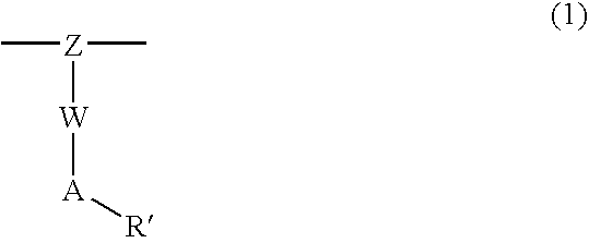
  • The present invention also refers to the novel composition where polymer B comprises a unit of structure 1,
  • Figure US20090042148A1-20090212-C00001
  • where Z is the polymer backbone, W is a single bond or a spacer group, A is an acid group without a proton and R′ is hydrogen or an acid labile group.
  • The novel composition also refers to the novel: composition where polymer B comprises a unit of structure 2,
  • Figure US20090042148A1-20090212-C00002
  • where Z is the polymer backbone, W is a single bond or a spacer group, X1 and X2 are partially or fully fluorinated (C1-C6) alkyl groups, b=1-6, A is an acidic group without a proton, and R′ is selected independently from hydrogen and an acid labile group.
  • The invention also refers to a process of imaging the above compositions.
  • BRIEF DESCRIPTION OF THE DRAWINGS
  • FIG. 1 refers to examples of monomers
  • FIG. 2 refers to further Examples of monomers
  • FIG. 3 refers to examples of monomers with R3 group
  • FIG. 4 refers to examples of monomers with R4 group
  • FIG. 5 examples of monomers with R5 group
  • FIG. 6 Examples of suitable ammonium bases.
  • DETAILED DESCRIPTION OF THE INVENTION
  • The present invention relates to a novel photoresist composition comprising (1) a polymer A comprising at least one acid labile group, (ii) at least one photoacid generator, (iii) at least one base, (iv) a polymer B, where polymer B is non-miscible with polymer A and also soluble in the coating solvent, and, (v) a coating solvent composition. The present invention also relates to a process for imaging the novel composition, especially in immersion lithography.
  • The present novel composition comprises a blend of at least two polymers A and B, where all the polymers are soluble in the coating solvent but at least one polymer (B) is non-miscible with the other polymer(s) B. A non-miscible polymer is one which under certain conditions will separate in the coated film. Polymer A is a polymer typically used in dry lithography and comprises at least one acid labile group. In the present invention non-miscible refers to the separation of the non-miscible polymer in the photoresist film during the coating and/or baking step of the photoresist, such that some of or the entire non-miscible polymer B essentially migrates towards the surface of the photoresist film. The surface migration of the polymer provides the photoresist with an in-situ barrier or protective coat which can prevent leaching of undesirable materials from the photoresist and provide an in-situ top coat within the coated photoresist layer with desirable properties. Polymer B comprises at least one group which makes the polymer nonmiscible with Polymer A and such a group may be a fluorinated acidic group or fluorinated acidic group capped with an acid labile group. The fluorinated acidic group may be fluorinated alcohol, fluorinated thiol, fluorinated carboxylic acid, fluorinated sulfonic acid, fluorinated sulfonamide, etc. In one embodiment of Polymer B, the non-miscible polymer B may comprise an acid labile group, where the acid labile group prior to exposure of the photoresist provides the photoresist surface with a high water contact angle, but after post exposure bake the acid labile group is completely or partially removed to form a hydrophilic polymeric surface which has in the exposed regions, a lower developer contact angle than prior to exposure. The lower developer contact angle assists in providing good development profiles of the imaged photoresist, especially free of scum residues.
  • In one embodiment of Polymer B, which is soluble in the coating solvent, Polymer B comprises an acid labile group. In another embodiment of Polymer B the polymer comprises an acid labile group and a halogenated acidic group. In yet another embodiment of Polymer B, the polymer comprises no acid labile group but comprises a halogenated acidic group, such as a fluoroalcohol group. Where the polymer B comprises an acidic group, the polymer is essentially insoluble in an aqueous alkali solution prior to exposure but becomes aqueous alkali soluble prior to development. The polymer B may be a homopolymer or polymer comprising more than one monomeric unit. Polymer B can comprise an acid labile group which may be obtained by reacting an acidic group in the polymer with a compound capable of forming an acid labile group, The acidic group on the polymer may be selected from fluoroalcohol, fluorothiol, carboxylic acid, sulfonic acid and sulfonamide. The acidic proton of the acidic group reacts with compounds such as chloromethylmethylether and tertiarybutyl bromoacetate to form an acid labile group capable of deprotecting in the presence of a strong acid. The polymer may be fully protected or partially protected. The polymer may be poly(meth)acrylate, polyvinylether, polyalkylene, polyfluorinatedalkylene, or a copolymer of poly(alkylene-co-(meth)acrylate) or poly(fluorinatedalkylene-co-(meth)acrylate), etc. The polymer B may comprise halogen (F, Br, I) or silicon to provide the appropriate nonmiscibility properties, and preferably fluorine Polymer B may be represented by the structure 1,
  • Figure US20090042148A1-20090212-C00003
  • where Z is the polymer backbone, W is a single bond or a spacer group, A is an acid group without a proton and A can be selected from oxygen (O), sulfur (S), carboxyl (C(O)O), sulfonyl (SO3) and sulfonamidyl (SO2NH), and R′ is selected independently from hydrogen and an acid labile group. The functionality (-AH) is capable of reacting with a compound to form the acid labile group (R′), which can deprotect in the presence of a strong acid to form the polymer comprising the group -AH. In one example the unit of structure 1 is fluorinated. In another example the unit of structure 1 is not fluorinated and the polymer further comprises monomeric units with fluorinated acidic groups, i.e. R′ is an acid labile group. In yet another example the polymer, R′ is hydrogen and no acid labile groups are present, specifically W is fluorinated,
  • Polymer B may be represented by structure 2,
  • Figure US20090042148A1-20090212-C00004
  • where Z is the polymer backbone, W is a single bond or a spacer group, X1 and X2 are partially or fully fluorinated (C1-C6) alkyl groups, b=1-6, A is an acidic group without a proton, and A is selected from oxygen (O), sulfur (S), carboxyl (COO), sulfonyl (SO3) and sulfonamidyl (SO2NH), and R′ is selected independently from hydrogen and an acid labile group. W, A and R′ are described herein.
  • In structure 1 and 2, Z is the polymeric backbone, such as alkylene which is unfluorinated or fully or partially fluorinated alkylene, etc. The alkylene, unfluorinated or fully or partially fluorinated alkylene, may be linear, branched, cyclic or mixture of these, Z may be a partially fluorinated cycloalkylene group or comprise a mixture of monomeric units which are partially fluorinated cycloalkylene group and fluorinated alkylene group. The cycloalkylene group may be 5 or 6 membered ring moiety. Specific examples of Z are shown in structure 3 and 4 a, b, c, d and e, and mixtures of these may be used, structures 4b-4e may be further fluorinated:
  • Figure US20090042148A1-20090212-C00005
  • where ‘n’ can be zero to 3 and C1 to C8 can be attached to hydrogen or fluorine independent of one another.
  • Figure US20090042148A1-20090212-C00006
  • In the polymer B, as shown in the previous structures 1 and 2, W is a single valence bond connecting the pendant moiety to the backbone or W may be a connecting or spacer group connecting the pendant moiety, A, to the backbone. Preferably W is nonaromatic group. Examples of W as a spacer group can be an organic group, and examples of an organic group are an aliphatic cyclic alkylene group, aliphatic linear or branched alkylene group, fully or partially fluorinated aliphatic cyclic alkylene group, fully or partially fluorinated aliphatic linear or branched alkylene group, carbonyl (CO)f, carbonyloxy or carboxyl (C(O)—O), oxycarbonyl (O—C(O)), carbonate (O—C(O)'O), sulfone (SO2), sulfoxide (SO), oxy (O), sulfide (S), aliphatic cyclic alkylene group with a pendant group selerted from carbonyl (CO), carbonyloxy (C(O)—O), oxycarbonyl (O—C(O)), carbonate (O—C(O)—O), sulfone (SO2), sulfoxide (SO), oxy (O), sulfide (S); and mixtures of these groups. Preferably, W in structures 1 and 2 may be O, (C(O)—O), O—fluoroalkylene-C(O)—O, alkylene, fully or partially fluorinated alkylene, and fully or partially fluorinated alkylene oxy or mixtures of these. Preferably, W in structure 2 may be a single bond, O, (C(O)—O), X1 and X2 are independently an (C1-C6) alkyl group which maybe fully or partially substituted with fluorine. Examples of X1 and X2 may be CF3, CHF2, CFH2, where b is 1-4. R′ is hydrogen or an acid labile group which in the presence of a strong acid is removed and is described herein.
  • The polymer B may be a homopolymer of structure 1 or 2, or a copolymer comprising a monomeric unit of structure 1 or 2 and at least one other monomeric unit. Examples of comonomers useful for obtaining Polymer B are given in FIGS. 1 to 5, which may comprise an acid labile group. Further examples of polymer B are shown below.
  • Polymer B such as those comprising structures 5 and 6 may also be used.
  • Figure US20090042148A1-20090212-C00007
  • where X is H or halogen (F, Br, I), (CX2) is fully or partially fluorinated alkyl, a=1-6, b=1-6, m and n are integers, R10 is an acid labile group or hydrogen, R11 is selected independently from hydrogen and an nonlabile group such as alkyl, R14 is substituted or unsubstituted alkylene, Alkylene includes, linear, branched or cyclic group such as cyclo butane, pentane, hexane, norbornene, tricyclododecene. The alkylene may be substituted with groups such as halogen, hydroxyl, carboxylic groups. R14 can be a fluorinated or unsubstituted alkylene. R15 is alkylene or halogen substituted alkylene, YH is hydroxyl, thiol, carboxylic acid, sulfonic acid, sulfonamide, R10 is any group cleavable by acid, and m and n are integers
  • Further examples of monomeric units of structure 1 or 2 in polymer B, are given in structure 7 and 8,
  • Figure US20090042148A1-20090212-C00008
  • where m and n are integers and Rx and Ry are independently selected from alkyld substituted alkyl, cycloalkyl, and substituted cycloalkyl and comprise at least one hexafluoroalcohol group which is free or protected with an acid labile group. Rx and Ry can be identical or different. Rx can be free of protection; as an example a copolymer of 3,5-Bis(hexafluoro-2hydroxy-2-propyl)cyclohexyl methacrylate and 1-cyclo hexyl-4,4,4-trifluoro-3-hydroxy-3-(trifluromethyl )but-1-yl methacrylate.
  • Further examples of polymer B comprise the unit of structure 9,
  • Figure US20090042148A1-20090212-C00009
  • where m, n and p are integers. X10-X18 are independently selected from H, alkyl and halogen (preferably F). R14 is substituted or unsubstituted alkylene. R14 includes cycloalkylene group such as cyclobutane, cyclopentane, cyclohexane, norbornene, and tricyclododecene, which may be unsubstituted or substituted with halogen. The alkylene may be substituted with fluorine. R15 is alkylene or halogen substituted alkylene, R16 is a carboxy group, YH is hydroxy or thiol or carboxylic acid group, R17 is any group cleavable by acid and R18 is any lactone group. Lactone containg monomers are exemplified in FIG. 3.
  • Another example of polymer B is given in structure 10,
  • Figure US20090042148A1-20090212-C00010
  • where s and t are integers. X is H or halogen. Preferably halogen is fluorine. R14 is substituted or unsubstituted alkylene, including cycloalkylene groups such as cyclobutane, cyclopentane, cyclohexane, norbomene, and tricyclododecene. The alkylene may be substituted with groups such as halogen, hydroxy, carboxylic groups. R14 can be substituted with fluorine. R15 is alkylene or halogen substituted alkylene. Preferably halogen is fluorine. YH is hydroxy or thiol or carboxylic acid group. Preferably YH is hydroxy. In one example YH is hydroxy and free of capping. The polymer of structure 10 may be further reacted to give a polymer which is fully or partially capped with an acid labile group, i.e. YH is reacted to give an acid labile group.
  • Polymer B may be as shown in structure 11
  • Figure US20090042148A1-20090212-C00011
  • where R, R1, R2, R3, R4, R5, m, n, o, p, q are as explained in the general structure for polymer A in structure 14, and R13 is any group that increases the water contact angle compared to the polymer without this group. R13 is for example halogen containing group, such as an acidic fluoroalcohol or fluorocarboxylic acid substituted alkyl groups, where the alkyl groups may be perfluoro adamantyl, perfluoro norbornyl, perfluoro cyclohexyl, perfluoro cyclopentyl perfluoro butyl, perfluoro ethyl etc., r may represent 40-100 mole % of the polymer.
  • Specific examples of polymer B are given in structures 12 and 13,
  • Figure US20090042148A1-20090212-C00012
  • where n, m and p are integers.
  • Polymer B may be a homopolymer or a copolymer comprising units of structure 1 to 10 and other comonomeric unit(s). Comonomeric units may be such as those in FIGS. 1-5. Copolymer B may contain about 30 mol % to 99 mole % of structure 1-10, and preferably about 40 mol % to about 80 mole %.
  • In the various embodiments, examples of acid labile groups are acetal protecting groups exemplified by alkyloxyalkyl, such as methyloxymethyl, adamantyl methyloxymethyl, bicyclohexyloxymethyl, ethyloxymethyl, menthyloxymethyl, and cyclopentyloxymethyl; acetal type esters may be used, such as ethoxymethylester, 1-ethoxyethylester, 1-isobutoxyethylester, 1-isopropoxyethylester, 1-ethoxypropylester, 1-(2-methoxyethoxy)ethylester, 1-(2-acetoxyethoxy)ethylester, 1-[2-(1-adamantyloxy)ethoxy]ethylester, 1-[2-(1-adamantancarbonytoxy)etho-xylethylester, tetrahydro-2-furylester and tetrahydro-2-pyra nylester, 2-alkyl-2-adamantyl, 1-adamantyl-1-alkylalkyl and alicyclic ester such as isobornylester, or acid cleaveable alkoxycarbonyl (e.g. tert-butoxycarboxyl, t-BOC), alkyleneoxyalkyl groups, trialkylsilyi, and 2-(trialkylsilyl)ethyl. Acid labile groups may be incorporated into any of the suitable monomeric units of the polymer:.
  • Polymer B may only comprise one or more types of units of structure 1 to structure 13. Specific examples of Polymer B are poly(1,1,2-Trifluoro-4-[2,2,2-trifluoro-1-hydroxy-1-trifluoromethylethyl]-1,6-heptadiene)(TFTFHTFMH) preferably protected with an acid labile group such as methoxymethyl group at suitable levels; a 50/50 copolymer of 3,5-Bis(hexafluoro-2hydroxy-2-propyl)cyclohexyl methacrylate and 1-cyclohexyl-4,4,4-trifluoro-3-hydroxy-3-(trifluromethyl)but-1-yl methacrylate as represented by structures 7 & 8; and a copolymer of (structure 4) [2-fluoro-2-hexafluoroisopropylhydroxymethyl]-5-norbornene and tetrafluoroethylene.
  • Polymer B may be made by free radical polymerization of mixtures of suitable monomers using Perkadox-16 free radical initiator in tetrahydrofuran (THF) and recovering the polymer using appropriate non-solvents. The weight average molecular weight may range from about 1000 to about 100, 000, preferably 2000 to about 30,000. Polymer B as the weight % of the photoresist polymer may range from about 0.1 to about 25 weight %, or about 0.1 to about 10 weight %, or 0.1 to about 5 weight %. The polymer B alone or as in the novel photoresist and in-situ separated can have a water contact angle from about 70° to about 95° before exposure in water. preferably from about 75° to about 95°. In one example the water contact angle is from about 80° to about 95°. Similarly, Polymer B can have an aqueous alkali developer contact angle from about 70° to about 90° before exposure, or in the range of about 70° to about 85°. After exposure and baking to remove some or the entire acid labile group in Polymer B. the polymer can have an aqueous alkali developer contact angle of less than 75°, or in the range of about 50° to about 70°. Typically, polymer A has a water contact angle of about 50° to about 75° before exposure. Thus a photoresist comprising a mixture of polymer A and B gives a coating with a higher water contact angle than a coating without polymer B. In addition to the contact angle limitations, the leaching of the components out of the novel photoresist film is less than or equal to 1.6×10⁻¹² mol/cm2/sec.
  • Polymer A comprises at least one acid labile group, which is removed in the presence of a strong acid. Polymer A may be a polymer which is typically used in a photoresist composition for non-immersion lithography, i.e. dry lithography. Such polymers are typically poly(meth)acrylates with no or very small amount (less than 1 mole %) of fluorine or silicon. Polymer A is not miscible with polymer B in the photoresist film coating. Examples of monomers that can be used to form polymer A are given in FIG. 1-5 Polymer A may contain any number of different comonomeric units, and may be 3, 4, 5 or 6 different units. One or more types of acid labile units may be present in the polymer. Examples of acid labile groups have been given previously. An example of suitable Polymer A is given in structure 14, comprising at least 4 different monomeric units (i) to (iv) and optionally (v),
  • Figure US20090042148A1-20090212-C00013
  • where R is H, substituted alkyl, unsubstituted alkyl; R1 to R5 is independently selected from a group comprising an acid labile group, a group comprising substituted or unsubstituted lactone, a group comprising substituted or unsubstituted alkyl group. In one example of Polymer A, R1 is an acid labile group, R2 is another acid labile group different from R1, R3 is a group comprising a lactone group, R4 is a substituted or unsubstituted alkyl, and optionally, R5 is independently selected from an acid labile group, a group comprising a substituted or unsubstituted lactone, and substituted or unsubstituted alkyl groups Examples of monomers used to form the polymer of structure 14 are given in FIG. 1 and 2, FIG. 3 refers to examples of R3. FIG. 4 refers to examples of R4. FIG. 4 refers to examples of R5. In one specific example of Polymer A, the polymer comprises R1 which is an acid cleavable group and R2 which is a different acid cleavable group.
  • Other types of polymers may also be used, such as norbornene based polymers, norbornene and acrylate copolymers, etc. Useful polymers are described in the following US patents and applications, U.S. Pat. No. 6,991,888 and U.S. Pat. No. 7,122,291, and application Ser. No. 11/623335 (of Jan. 16, 2007).
  • The weight average molecular weight of the Polymer A may range from about 2000 to about 100,000 preferably 3000 to about 30,000. Typically Polymer A has a water contact angle from about 50° to about 75° prior to exposure.
  • In the above definitions and throughout the present specification, unless otherwise stated the terms used are described below.
  • Alkyl means linear or branched alkyl having the desirable number of carbon atoms and valence. The alkyl group is generally aliphatic and may be cyclic or acyclic (i.e. noncyclic). Suitable acyclic groups can be methyl, ethyl, n-or iso-propyl, n-,iso, or tert-butyl, linear or branched pentyl, hexyl, heptyl, octyl, decyl, dodecyl, tetradecyl and hexadecyl. Unless otherwise stated, alkyl refers to 1-20 carbon atom moeity. The cyclic alkyl groups may be mono cyclic or polycyclic. Suitable example of mono-cyclic alkyl groups include substituted cyclopentyl, cyclohexyl, and cycloheptyl groups. The substituents may be any of the acyclic alkyl groups described herein. Suitable bicyclic alkyl groups include substituted bicyclo[2.2.1]heptane, bicyclo[2.2.2]octane, bicyclo[3.2.1]octane, bicyclo[3.2.2]nonane, and bicyclo[3.3.2]decane, and the like. Examples of tricyclic alkyl groups include tricyclo[5.4.0.0.2,9]undecane, tricyclo[4.2.1.2.7,9jundecane, tricyclo[5.3.2.0.4.9]dodecane, and tricyclo[5.2.1.0.2,6]decane. As mentioned herein the cyclic alkyl groups may have any of the acyclic alkyl groups as substituents. Examples of multicyclic alkyl groups are adamantyl and norbornyl. Any of the alkyl groups may be substituted with halogen, such as fluorine; hydroxy, carboxylic acid, thiol, fluoroalcohol, etc.
  • Alkylene groups are divalent alkyl groups derived from any of the alkyl groups mentioned hereinabove. When referring to alkylene groups, these include an alkylene chain substituted with (C1-C6)alkyl groups in the main carbon chain of the alkylene group. Alkylene groups can also include one or more alkyne groups in the alkylene moiety, where alkyne refers to a triple bond. Essentially an alkylene is a divalent hydrocarbon group as the backbone. Accordingly, a divalent acyclic group may be methylene, 1,1- or 1,2-ethylene, 1,1-, 1,2-, or 1,3 propylene, 2,5-dimethyl-hexene, 2,5-dimethyl-hex-3-yne, and so on. Similarly, a divalent cyclic alkyl group may be 1,2- or 1,3-cyclopentylene, 1,2-, 1,3-, or 1,4-cyclohexylene, and the like. A divalent tricyclo alkyl groups may be any of the tricyclic alkyl groups mentioned herein above. A particularly useful tricyclic alkyl group in this invention is 4,8-bis(methylene)-tricyclo[5.2.1.02,6]decane.
  • Alkoxy means straight or branched chain alkoxy having 1 to 10 carbon atoms, and includes, for example, methoxy, ethoxy, n-propoxy, isopropoxy, n-butoxy, isobutoxy, tert-butoxy, pentyloxy, hexyloxy, heptyloxy, octyloxy, nonanyloxy, decanyloxy, 4-methylhexyloxy, 2-propylheptyloxy, and 2-ethyloctyloxy.
  • The term (meth)acrylate refers to methacrylate or acrylate, and similarly, (meth)acrylic refers to methacrylic or acrylic.
  • Furthermore, and as used herein, the term “substituted” is contemplated to include all permissible substituents of organic compounds. In a broad aspect, the permissible substituents include acyclic and cyclic, branched and unbranched, carbocyclic and heterocyclic, non-aromatic substituents of organic compounds. Illustrative substituents include, for example, those described hereinabove. The permissible substituents can be one or more and the same or different for appropriate organic compounds. For purposes of this invention, the heteroatoms such as nitrogen may have hydrogen substituents and/or any permissible substituents of organic compounds described herein which satisfy the valencies of the heteroatoms. This invention is not intended to be limited in any manner by the permissible substituents of organic compounds.
  • Organic groups refer to essentially hydrocarbon groups which may have substituents present. HFydrocarbyl and: hydrocarbylene groups are example of organic groups, further examples being alkyl, alkylene, alkoxy, etc.
  • The polymers of this invention can be synthesized using techniques known in the art. The polymer of this invention, especially those that can be synthesized by free radical polyvmerization technique, may use for example, 2,2′-azobisisobutyronitrile (AIBN) or a suitable peroxydicarbonate as initiator. A mixture of monomers or the mixture comprising a monomer of derived from structure 1, is added to a reaction vessel together with a solvent, e.g. tetrahydrofuran. and AIBN is added. The reaction is carried out at a suitable temperature for a suitable amount of time to give a polymer with desired properties. The reaction may also be carried out Without a solvent. The temperature may range from about 35° C. to about 150° C., preferably 50° C. to 90° C. for about 5 to 25 hours. The reaction may be carried out at atmospheric pressure or at higher pressures. It has been found that a reaction carried out under a pressure of from about 48,000 Pascals to about 250,000 Pascals gives a polymer with more consistent properties, where examples of such desirable properties are molecular weight, dark film loss, yield, etc. Dark film loss is a measure of the solubility of the unexposed photoresist film in the developing solution, and a minimal film loss is preferred. The polymer may be isolated from any suitable nonsolvent, such as, diethyl ether, hexane or mixture of both hexane and ether, methanol, etc. Other polymerization techniques may be used to obtain a polymer with the desired chemical and physical properties.
  • The contact angle of a material is measured using accepted methods. The leaching of the components of a photoresist out of the photoresist film can also be measured. The leaching of the components out of the novel photoresist film is less than or equal to 1.6×10⁻¹² mol/cm2/sec.
  • The novel photoresist comprises Polymer A, Polymer B, at least one photoacid generator and at least one base. The compound capable of producing an acid upon irradiation, a photoacid generator (PAG), of the novel composition is selected from those which absorb at the desired exposure wavelength, preferably 193 nm and 157 nm. Any suitable photoacid generator or mixture of photoacid generators may be used. Suitable examples of the acid generating photosensitive compounds include, without limitation, ionic photoacid generators (PAG), such as diazonium salts, iodonium salts, sulfonium salts, or non-ionic PAGs such as diazosulfonyl compounds, sulfonyloxy imides, and nitrobenzyl sulfonate esters. although any photosensitive compound that produces an acid upon irradiation may be used. The onium salts are usually used in a form soluble in organic solvents, mostly as iodonium or sulfonium salts, examples of which are diphenyliodonium trifluoromethane sulfonate, diphenyliodonium nonafluorobutane sulfonate, triphenylsulfonium trifluromethane sulfonate, triphenylsulfonium nonafluorobutane sulfonate and the like. Other compounds that form an acid upon irradiation that may be used, are triazines, oxazoles, oxadiazoles, thiazoles, substituted 2-pyrones. Phenolic sulfonic esters, bis-sulfonylmethanes, bis-sulfonylmethanes or bis-sulfonyldiazomethanes, triphenylsulfonium tris(trifluoromethylsulfonyl)methide, triphenylsulfonium bis(trifluoromethylsulfonyl)imide, diphenyliodonium tris(trifluoromethylsulfonyl)methide, diphenyliodonium bis(trifluoromethylsulfonyl)imide and their homologues are also possiible candidates. Mixtures of photoactive compounds may also be used, In some embodiments mixtures of photoacid generators is used. The photoresist can comprise a mixture of at least one sulfonium PAG and at least one iodonium PAG, exemplified by, but not limited to 1) a mixture of bis-triphenyllsulfonium octafluorobutaned isu Ifon ate, bis-tert. butyldiphenyliodonium octafluorobutanedisulfonate, and bis(tert.butylphenyl)iodonium bis(pentafluoroethanesulfonyl)imide and 2) a mixture of triphenylsulfonium perfluoropropanedisulfonylimide and bis(triphenylsulfonium) perfluorobutane-1,4-disulfonate, (TPSC4).
  • Bases or photoactive bases are added to the photoresist to control the profiles of the imaged photoresist and prevent surface inhibition effects, such as T-tops. Nitrogen containing bases are preferred, specific examples of which are amines, such as triethylamine, triethanolamine, aniline, ethylenediamnie, pyridine, tetraalkylammonium hydroxide or its salts. Examples of photosensitive bases are diphenyliodonium hydroxide, dialkyliodonium hydroxide, trialkylsulfonium hydroxide, etc. The base may be added at levels up to 100 mole % relative to the photoacid generator. Although, the term base additive is employed, other mechanisms for removal of acid are possible, for instance by using tetraalkylammonium salts of volatile acids (eg. CF3CO2 ) or nucleophilic acids (eg Br), which respectively remove acid by volatilization out of the film during post-exposure bake or by reaction of a nucleophilic moiety with the acid precursor carbocation (e,g. reaction of tert-butyl carbocation with bromide to form t-butylbromide).
  • FIG. 6 shows the structures of ammonium derivatives which might be employed as bases. Specific bases are shown in structures 15-19,
  • Figure US20090042148A1-20090212-C00014
  • The use of non volatile amine additives is also possible. Preferred amines would be ones having a sterically hindered structure so as to hinder nucleophilic reactivity while maintaining basicity, low volatility and solubility in the resist formulation, such as a proton sponge, 1,5-diazabicyclo[4.3.0]-5-nonene, 1,8-diazabicyclo[5,4,0]-7-undecene, cyclic akylamines, or polyether bearing amines such as described in U.S. Pat. No. 6,274,286. Mixtures of bases may also be used, such as a mixture of diisopropylaniline and trimethoxyethoxyethylamine, or a mixture of ditisopropylaniiine and phenyldiethanolamine or a mixture of diisopropylaniline and N(tert.butoxycarbonyl)-L-alanine methyl ester or a mixture of trimethoxyethoxyethylamine and trioctylamine.
  • In one embodiment of the present novel composition, it comprises a Polymer A, a Polymer B. a mixture of sulfonium and iodonium PAGs and mixture of diisopropylaniline and phenyidiethanolamine bases. Thus, copolymer obtained by polymerizing ethyladamantylmethacrylate, ethylcyclopentylmethacrylate, hydroxyadamantylacrylate and a-gammabutyrolactone methacrylate was blended with a polymer represented by Structure 1, more specifically structure 2 as represented by poly(1,1,2-Tritluoro-4-[2,2,2-trifluoro-1-hydroxy-1-trifluoromethylethyl]-1,6-heptadiene)(TFTFHTFMFH) that was 70 mole % protected with methoxymethyl group, along with diisopropylaniline and phenyidiethanolamine and bis-triphenylsulfonium: perfluorobutanedisulfonate, ditert.butyliodonium bis(pentafluoroethylsulfonyl)imide and bis-ditert.butyliodonium perfluorobutanedisulfonate.
  • In another example (7074), a terpolymer obtained by polymerizing Ethyladamantyvmethacrylate, hydroxyadamantyl acrylate and a-gammabutyrolactone acrylate was mixed with polymer represented by structure 1, more specifically structure 2 TFTFHMH that was 70 mole % protected with methoxymethyl group, tris[2-(2-methoxyethoxy)ethyllamine and triphenylsulfonium salt of perfluoropropyldisulfonylimide. In the third example, (83645), tetrapolymer obtained by polymerizing ethyladamantyimethacrylate, hydroxyadamantylacrylate, a-gammabutyrolactonemethacrylate and adamantylmethacrylate was mixed with polymer represented by structure 1, more specifically structure 2 and diisopropylaniline and bis-triphenylsulfonium perfluorobutanedisulfonate, ditert.butyliodonium bis(pentafluoroethylsulfonyl)imide and bis-ditert.butyliodonium perfluorobutanedisulfonate.
  • In another example (6733), a terpolymer obtained by polymerizing ethyidiamantylmethacrylate, hydroxyadamantylacrylate and gamma-butyrolactonemethacrylate was mixed with polymer whose structure is represented by srtucture 1, more specifically structure 2, TFTFHMH that was 70 mole % protected with methoxymethyl group, and diisopropylaniline and bis-triphenylsulfonium perfluorobutanedisulfonate, ditert.butyliodonium bis(pentafluoroethylsulfonyl)imide and bis-ditert.butyliodonium perfluorobutanedisulfonate.
  • In yet another example (6734), terpolymer obtained by polymerizing ethyidiamantyl methacrylate, hydroxyadamantyl acrylate and gamma-butyrolactone acrylate was mixed with polymer whose structure is represented in structure 1, more specifically structure 2 TFTFHMH that was 70 mole % protected with methoxymethyl group, and diisopropylaniline and bis-triphenylsulfonium perfluorobutanedisulfonate, ditert.butyliodonium bis(pentafluoroethylsulfonyi)mide and bis-ditert.butyliodonium perfluorobutanedisulfonate.
  • In another example, (7095) a copolymer obtained by polymerizing ethyladamantylmethacrylate, 3-oxo-1-adamantyloxymethyl methacrylate, hydroxyadamantylacrylate and a-gammabutyrolactone methacrylate was blended with a polymer represented by structurel, more specifically structure 2 TFTFHMH that was 70 mole % protected with methoxyrmethyl group, along with diisopropylaniline and phenyidiethanolamine and bis-triphenylsulfonium perfluorobutaneedisulfonate, ditert.butyliodonium bis(pentafluoroethylsulfonyllimide and bis-ditert.butyliodonium perhluorobutanedisulfonate.
  • In another example, (7295) a copolymer obtained by polymerizing Ethyladamantylmethacrylate, adamantyloxyrmethylmethacrylate, hydroxyadamantylacrylate and a-gammabutyrolactone methacrylate and adamantylmethacrylate was blended with a polymer represented by structure 1, more specifically structure 2 TFTFHMH that was 70 mole % protected with methoxymethyl group, along with diisopropylaniline and phenyldiethanolamine and bis-triphenylsulfonium perfluorobutanedisulfonate, ditert.butyliodonium bis(pentafluoroethylsulfonyl)imide and bis-ditert.butyliodonium perfluorobutanedisulfonate.
  • The photoresist of the present invention may contain other components as additives, such as surfactants, dyes, and other secondary polymers.
  • The photoresist composition is formed by blending the ingredients in a suitable photoresist solvent. In the preferred embodiment, the amount of polymer mixture in the photoresist preferably ranges from 90% to about 99.5% and more preferably from about 95% to about 99% based on the weight of the solid; i.e., non-solvent photoresist components. In the preferred embodiment, the photoactive compound is present in the photoresist in an amount of from about 0.5% to about 10% preferably from about 4% to about 6% based on the weight of the solid photoresist components.
  • The solid components of the antireflection coating composition are mixed with a solvent or mixtures of solvents that dissolve the solid components of the antireflective coating. Suitable solvents for the antireflective coating composition may include, for example, a glycol ether derivative such as ethyl cellosolve, methyl cellosolve, propylene glycol monornethyl ether, diethylene glycol monomethyl ether, diethylene glycol: monoethyl ether, dipropylene glycol dimethyl ether, propylene glycol n-propyl ether, or diethylene glycol dimethyl ether; a glycol ether ester derivative such as ethyl cellosolve acetate, methyl cellosolve acetate, or propylene glycol monomethyl ether acetate; carboxylates such as ethyl acetate, n-butyl acetate and amyl acetate; carboxylates of di-basic acids such as diethyloxylate and diethylmalonate; dicarboxylates of glycols such as ethylene glycol diacetate and propylene glycol diacetate; and hydroxy carboxylates such as methyl lactate, ethyl lactate, ethyl glycolate, and ethyl-3-hydroxy propionate, a ketone ester such as methyl pyruvate or ethyl pyruvate; an alkoxycarboxylic acid ester such as methyl 3-methoxypropionate, ethyl 3-ethoxypropionate, ethyl 2-hydroxy-2-methylpropionate, or methylethoxypropionate; a ketone derivative such as methyl ethyl ketone, acetyl acetone, cyclopentanone, cyclohexanone or 2-heptanone; a ketone ether derivative such as diacetone alcohol methyl ether; a ketone alcohol derivative such as acetol or diacetone alcohol; a ketal or acetal like 1,3 dioxalne and diethoxypropane; lactones such as butyrolactone and gamma valerolactone; an amide derivative such as dimethylacetamide or dimethylformamide, anisole, and mixtures thereof. Mixtures of solvents are also used.
  • The prepared photoresist composition solution can be applied to a substrate by any conventional method used in the photoresist art, including dipping, spraying, whirling and spin coating. When spin coating, for example, the photoresist solution can be adjusted with respect to the percentage of solids content, in order to provide coating of the desired thickness, given the type of spinning equipment utilized and the amount of time allowed for the spinning process. Suitable substrates include silicon, aluminum, polymeric resins, silicon dioxide, doped silicon dioxide, silicon nitride, tantalum, copper, polysilicon. ceramics, aluminum/copper mixtures; gallium arsenide and other such Group III/V compounds. The photoresist may also be coated over antireflective coatings.
  • The photoresist composition solution is then coated onto the substrate, and the substrate is treated at a temperature from about 70° C. to about 150° C. for from about 30 seconds to about 180 seconds on a hot plate or for from about 15 to about 90 minutes in a convection oven. This temperature treatment is selected in order to reduce the concentration of residual solvents in the photoresist, while not causing substantial thermal degradation of the solid components, In general, one desires to minimize the concentration of solvents and this first temperature treatment is conducted until substantially all of the solvents have evaporated and a thin coating of photoresist composition, on the order of half a micron (micrometer) in thickness, remains on the substrate. In a preferred embodiment the temperature is from about 95° C. to about 160° C., and more preferably from about 95° C. to about 135° C. The treatment is conducted until the rate of change of solvent removal becomes relatively insignificant. The temperature and time selection depends on the photoresist properties desired by the user, as well as the equipment used and commercially desired coating times. The coating substrate can then be imagewise exposed to actinic radiation, e.g., ultraviolet radiation, at a wavelength of from about 100 nm (nanometers) to about 300 nm, x-ray, electron beam, ion beam or laser radiation, in any desired pattern, produced by use of suitable masks, negatives, stencils, templates, etc.
  • In the embodiment where immersion lithography is used to expose the photoresist, the photoresist coating may optionally have a top coating to prevent contamination problems. The coating substrate can then be imagewise exposed to actinic radiation by immersion lithography, e.g., ultraviolet radiation, at a wavelength of from about 100 nm (nanometers) to about 450 nm, x-ray, electron beam, ion beam or laser radiation, in any desired pattern, produced by use of suitable masks, negatives, stencils, templates, etc. A typical immersion liquid used comprises water
  • The photoresist is then subjected to a post exposure second baking or heat treatment before development. The heating temperatures may range from about 90° C. to about 160° C., more preferably from about 100° C. to about 130° C. The heating may be conducted for from about 30 seconds to about 5 minutes, more preferably from about 60 seconds to about 90 seconds oh a hot plate or about 15 to about 45 minutes by convection oven.
  • The exposed photoresist-coated substrates are developed to remove the image-wise exposed areas by immersion in a developing solution or developed by spray, puddle or spray-puddle development process. The solution is preferably agitated, for example, by nitrogen burst agitation. The substrates are allowed to remain in the developer until all, or substantially all, of the photoresist coating has dissolved from the exposed areas. Developers include aqueous solutions of ammonium or alkali metal hydroxides or supercritical carbon dioxide. One preferred developer is an aqueous solution of tetramethyl ammonium hydroxide. Surfactants may also be added to the developer composition. After removal of the coated wafers from the developing solution, one may conduct an optional post-development heat treatment or bake to increase the coating's adhesion and chemical resistance to etching conditions and other substances. The post-development heat treatment can comprise the baking of the coating and substrate below the coating's softening point or UV hardening process. in industrial applications, particularly in the manufacture of microcircuitry units on silicon/silicon dioxide-type substrates, the developed substrates may be treated with a buffered, hydrofluoric acid etching solution or preferably, dry etching. In some cases metals are deposited over the imaged photoresist.
  • Each of the documents referred to above are incorporated herein by reference in its entirety, for all purposes. The following specific examples will provide detailed illustrations of the methods of producing and utilizing compositions of the present invention. These examples are not intended, however, to limit or restrict the scope of the invention in any way and should not be construed as providing conditions, parameters or values which must be utilized exclusively in order to practice the present invention.
  • EXAMPLES
  • Static contact angle (SCA) data were collected using VCA 2500XE (Video Contact Angle System) from AST Products, Inc. (9 Linnell Circle, Billerica, Mass. 01821) using OmniSolv water from EM Science (480 Democrat Road, Gibbstown, N.J. 08027) or AZ® 300MIF Developer (available from AZ Electronic Materials USA Corp., 70, Meister Ave., Somerville, N.J. 08876). Tests were carried out in Glass-1000 Fab environment. Static contact angle were reported as average value from more than six measurements.
  • The leaching of the components of a photoresist out of the photoresist film was measured by O-ring method. 60 s of soaking time, 8 ml of water and 20 cm2 of water-material surface contact area were employed. PAG anion concentration in ng/ml of water sample was measured using Liquid Chromatography/Mass Spectroscopy/Mass Spectroscopy LC/MS/MS technique.
    • EAdMA refers to 2-ethyl-2-ad amantylmethacrylate
    • ECPMA refers to 2-ethyl-2-cyclope ntyl methacrylate
    • HAdA refers to 3-hydroxy-1-adamantylacrylate
    • a-GBLMA refers to alpha-gammabutyrolactonemethacrylate
    • EDiMA refers to 2-ethyl-2-diamantyimethacryalte
    • AdOMMA refers to Adamantyloxymethylmethacrylate
    • AdMA refers to Ad amantylmethacrylate
    • EDIMA refers to 2-ethyl-2d-diamantylmethacrylate
    • AdOM MA(3) refers to 3-OXO-1-adama ntyloxymethylmethacryalte
    EXAMPLE 1 Synthesis of Poly(EAdM-A/ECPMA/HAdA/a-GBLMA)
  • In a 500 mL 4-neck flask were taken 18.69 g of EAdMA, 13.74 g of ECPMA, 33.45 g of HAdA, 34.19 g of a-GBLMA and 5 g of Perkadox-16 free radical initiator (available Akzo-Nobel Polymer Chemicals, LLC, 300 South riverside Plaza, Chicago, Ill. 60606, USA) along with 156 g of tetrahydrofuran (THF) solvent. The contents of the flask were allowed to become homogeneous while stirring and a dynamic blanket of nitrogen was provided. Once homogeneous, the contents of the flask were brought to reflux and reflux continued for 5 hours. At the end of 5 hours, the reaction contents were brought down to room temperature and precipitated in methanol and then in hexanes and dried in vacuo to obtain 55 g of polymer with an Mw of 17,414 with a polydispersity of 1.49.
  • EXAMPLE 2 Synthesis of Poly(EAdMA/HAdA/a-GBLMA)
  • In a 3 L 4-neck flask were taken 350.95 g of EAdMA, 125.55 g of HAdA, 132.38 g of a-GBLA and 91.30 g of AIBN free radical initiator along with 1300 g of THF. The synthetic method as in example 1 was used. 352 g of polymer with an Mw of 8,866 with a polydispersity of 1.70 was obtained.
  • EXAMPLE 3 Synthesis of Poly(EAdMA/HAdA/a-GBLMA/AdMA)
  • In a 3 L 4-neck flask were taken 237.68 g of EAdMA, 142 g of HAdA, 218.20 g of a-GBLMA, 70.30 g of Adamantylmethacrylate and 33.26 g of perkadox-16 free radical initiator along with 1300 g of THF. The synthetic method as in example 1 was used. 496 g of polymer with an Mw of 14,963 with a polydispersity of 1.92 was obtained.
  • EXAMPLE 4 Synthesis of Poly(EDiMA/HAdA/a-GBLA)
  • In a 500 mL 4-neck flask were taken 14.06 g of EDiMA, 10.36 g of HAdA, 9.72 g of a-GBLA and 3.39 g of Perkadox-16 free radical initiator along with 112.50 g of THF. The synthetic method as in example 1 was used. 11.82 g of polymer with an Mw of 9913 with a polydispersity of 1.57 was obtained.
  • EXAMPLE 5 Synthesis of Poly(EAdMA/AdOMMA(3)/HAdA/a-GBLMA)
  • In a 500 mL 4-neck flask were taken 8.61 g of EAdMA, 9.19 g of AdOMMA(3), 20.52 g of HAdA, 11.82 g of a-GBLMA and 5 g of Perkadox-16 free radical initiator along with 165 g of THF The synthetic method as in example 1 was used. 18.36 g of polymer with an Mw of 11,131 with a polydispersity of 1.63 was obtained.
  • EXAMPLE 6 Synthesis of Poly(EDiMA/HAdA/a-GBLMA)
  • In a 500 mL 4-neck flask were taken 15.28 g of EDiMA, 11.32 g of HAdA, 7.46 g of a-GBLMA and 3.39 g of Perkadox-16 free radical initiator along with 112.50 g of THF. The synthetic method as in example 1 was used. 15.97 g of polymer with an Mw of 9657 with a polydispersity of 1.61 was obtained.
  • EXAMPLE 7 Synthesis of Poly(EAdMA/AdOMMA(3)/HAdA/a-GBLMA/AdMA)
  • In a 500 mL 4-neck flask were taken 16 g of EAdMA, 7.98 G of AdOMMA, 14.20 g of HAdA, 21.62 g of a-GBLMA. 7.20 g of AdMA and 3.31 g of Perkadox-16 free radical initiator along with 130 g of THF. The synthetic method as in example 1 was used. 57 g of polymer with an Mw of 18,291 with a polydispersity of 2.21 was obtained.
  • COMPARATIVE PHOTORESIST EXAMPLE 1
  • 1.2151 g of Poly(EAdMA/ECPMA/HAdA/a-GBLMA) 15/15130140 polymer made in polymer synthesis example (1), 0.0282 g of bis(p-tertbutyl phenyl)iodonium perfluoroethanesulfonylimide (BDPINC2), 0.0323 g of bis(triphenylsulfonium) perfluorobutane-1,4-disulfonate, (TPSC4), 0.0655 grams of bis(p-tertiarybutylphenyl)iodonium perfluorobutane-1,4-disulfonate, 0.0071 grams of N,N-diisopropylaniline, 0.0018 g of phenyl-N,N-diethanolamine, 0.0036 grams of FC4430 surfactant supplied by 3M Corporation Were dissolved in 22.6545 g of methylalphahydroxyisobutyrate (MHIB) and 5.6007 g of propyleneglycolmonomethylether and 0.3912 g of gamma valerolactone. The solution was thoroughly mixed for complete dissolution and filtered using 0.2 um filter.
  • A silicon substrate coated with a bottom antireflective coating (B.A.R.C.) was prepared by spin coating the bottom anti-reflective coating solution (AZ® ArF-38, B.A.R.C. available from AZ® Electronic Materials Corporation, Somerville, N.J., USA) onto the silicon substrate and baking at 225° C. for 90 sec. The B.A.R.C film thickness was 87 nm. The photoresist solution prepared in this Example was then coated on the B.A.R.C coated silicon substrate. The spin speed was adjusted such that the photoresist film thickness was 120 nm, soft baked at 100° C./60 s, exposed with Nikon 306D 0.85NA 193 nm radiation, and dipole illumination using 6% half-tone mask. The exposed wafer was post exposure baked at 110° C/60 s, and developed using a 2.38 weight % aqueous solution of tetramethyl ammonium hydroxide for 30 sec. The line and space patterns were then measured on a AMAT 3D CD SEM (scanning electron microscope). The photosensitivity to print 70 nm (1:1) trench photoresist pattern without mask bias was 37 mJ/cm2, with a depth of focus (DoF) of 0.325 um and the average 3sigma line edge roughness/line width roughness (LER/LWR) at ±0.10 μm DoF was 4.48 J 6.60 nm. This photoresist exhibited a static water contact angle of 63.05°
  • COMPARATIVE PHOTORESIST EXAMPLE 2
  • 2.9049 g of Poly(EAdMA/HAdA/a-GBLA) 50/20/30 polymer made in polymer synthesis example (2), 0.0549 g of triphenylsulfonium perfluoropropanesulfonylimide (TPS_PFSI_Cy6), 0.0258 g of bis(triphenylsulfonium) perfluorobutane-1,4-disulfonate, (TPSC4), 0.0145 g of tris[2-(2-methoxyethoxy)ethyl]amine, 0.0060 grams of FC4430 surfactant supplied by 3M Corporation were dissolved in 46.9940 g of a 60/40 (w/w) mixture of propyleneglycol monomethylether acetate and ethyl lactate. The solution was thoroughly mixed for complete dissolution and filtered using 0.2 um filter.
  • A silicon wafer coated with a bottom antireflective coating (B.A.R.C.) was prepared by spin coating the bottom anti-reflective coating solution (AZ® 1C5D, B.A.R.C. available from AZ Electronic Mhaterials Corporation, Somerville, N.J.) onto the silicon substrate and baking at 200° C. for 60 sec. The B.A.R.C film thickness was 37 nm. The photoresist solution prepared in this Example was then coated on the B.A.R.C coated silicon substrate. The spin speed was adjusted such that the photoresist film thickness was 150 nm, soft baked at 105° C./60 s, exposed with Nikon 306D 0.85NA & conventional illumination using 6% half-tone mask. The exposed wafer was post exposure baked at 120° C./60 s, and developed using a 2.38 weight % aqueous solution of tetramethyl ammonium hydroxide for 60 sec. The photoresist contact hole patterns were then inspected using a AMAT 3D CD SEM. The photosensitivity to print 90 nm contact hole with pitch 200 nm photoresist pattern with 30 nm mask bias was 56 mJ/cm2, with a DoF of 0.25 um.
  • PHOTORESIST EXAMPLE 3
  • 0.012 g of homopolymer of 1,1,2-trifluoro-4-(2,2,2-trifluoro-1-hydroxy-1-trifluoromethylethyl)-1,6-heptadiene (CF2═(═FCH2CH(C(CF3)2(OH))CH2CH═CH2 (TFTFHMH)), that was 70 mole % protected with methoxymethyl group,corresponding to 1 weight percent of polymer (available from Asahi Glass Co., Ltd., 12-1 Yurakucho 1-Chome, Chiyoda-Ku, Tokyo 100-8405, Japan) was mixed with 30 g of photoresist from Comparative Example 1. The resultant mixture was placed on a roller for 8 h and filtered using 0.2 um filter.
  • The photoresist of this example was processed in the same manner as described in Comparative Photoresist Example 1. The photoresist had a photosensitivity of 38 mJ/cm2 for printing 70 nm (1:1) trench without mask bias, with a DoF of 0.30 um, and the average 3sigma LER/LWR values at ±0.10 um DoF was 4.88 and 7.17 nm respectively.
  • The photoresist of this example had a water static contact of 87.53° and was much higher than that of the Comparative Photoresist Example 1.
  • PHOTORESIST EXAMPLE 4
  • 0.0230 g of homopolymer of (TFTFHMH), that was 70 mole % protected with methoxymethyl group corresponding to 2 weight percent of photoresist polymer (available from Asahi Glass Co., Ltd., Japan) was mixed with 30 g of photoresist from Comparative Example 1. The resultant mixture was placed on a roller for 8 h and filtered using 0.2 um filter.
  • The photoresist solution prepared in this Example was then coated on the B.A.R.C coated silicon substrate. The spin speed was adjusted such that the photoresist film thickness was 120 nm, and soft baked at 100° C./60 s. This photoresist gave a static water contact angle of 92.20°, which was much higher than Comparative Example 1.
  • PHOTORESIST EXAMPLE 5
  • 0.0156 g of homopolymer of TFTFHMH that was 70 mole % protected with methoxymethyl group corresponding to 2.5 weight percent of polymer (available from Asahi Glass Co., Ltd., Japan.) was mixed with 15 g of photoresist from Comparative Example 1. The resultant mixture was placed on a roller for 8 h and filtered using 0.2 um filter.
  • The photoresist solution prepared in this Example was then coated on the B.A.R.C coated silicon substrate. The spin speed was adjusted such that the photoresist film thickness was 120 nm, soft baked at 100° C./60 s. This photoresist gave a static water contact angle of 92.52°, which was much higher than Comparative Example 1.
  • PHOTORESIST EXAMPLE 6
  • 0.0312 g of homopolymer of TFTFHMH that was 70 mole % protected with methoxymethyl group, corresponding to 5 weight percent of polymer (available from Asahi Glass Co., Ltd., Japan) was mixed with 15 g of photoresist from Comparative Example 1. The resultant mixture was placed on a roller for 8h and filtered using 0.2 um filter.
  • The photoresist solution prepared in this Example was then coated on the B.A.R.C coated silicon substrate. The spin speed was adjusted such that the photoresist film thickness was 120 nm, soft baked at 100° C./60 s. This photoresist gave a static water contact angle of 92.48° which was much higher than Comparative Example 1.
  • PHOTORESIST EXAMPLE 7
  • 0.0115 g of homopolymer of 1,1,2-trifluoro-4-(2,2,2-trifluoro-1-hydroxy-1-trifluoromethylethyl)-1,6-heptadiene (CF2═CFCH2CH(C(CF3)2(OH))CH2CH═CH2 (TFTFHMH)), that was 30 mole % protected with methoxymethyl group, corresponding to 1 weight percent of polymer (available from Asahi Glass Co., Ltd., Japan) was mixed with 30 g of photoresist from Comparative Example 1. The resultant mixture was placed on a roller for 8 h and filtered using 0.2 um filter.
  • The photoresist of this example was processed in the same manner as described in Comparative Photoresist Example 1. The photoresist solution prepared in this Example was then coated on the B.A.R.C coated silicon substrate. The spin speed was adjusted such that the photoresist film thickness was 420 nm, soft baked at 100° C./60 s, This photoresist gave a static water contact angle 85.55°
  • PHOTORESIST EXAMPLE 8
  • 0.0115 g of homopolymer of 1,1,2-trifluoro-4-(2,2,2-trifluoro-1-hydroxy-1-trifluoromethylethyl)-1,6-heptad iene (CF2═CFCH2CH(C(CF3)2(OH))C(H2CH═CH2 (TFTFHMH)), that was 50 mole % protected with methoxymethyl group corresponding to 1 weight percent of polymer (available from Asahi Glass Co., Ltd. Japan) was mixed with 30 g of photoresist from Comparative Example 1. The resultant mixture was placed on a roller for 8 h and filtered using 0.2 um filter,
  • The photoresist of this example was processed in the same manner as described in Comparative Photoresist Example 1 The photoresist solution prepared in this Example was then coated on the B.A.R.C coated silicon substrate. The spin speed was adjusted such that the photoresist film thickness was 120 nm, soft baked at 100° C./60 s. This photoresist gave a static water contact angle 81.83°
  • PHOTORESIST EXAMPLE 9
  • 0.0164 g of homopolymer of TFTFHMH that was 70 mole % protected with methoxymethyl group was mixed with 15 g of photoresist from Comparative Example 2. The resultant mixture was placed on a roller for 8h and filtered using 0.2 um filter.
  • The photoresist of this example was processed in the same manner as described in Comparative Example 2. The photoresist had a photosensitivity of 54 mJ/cm2 for printing 90 nm contact hole with a pitch of 200 nm photoresist pattern with 30 nm of mask bias. The DoF was 0.25 um.
  • The photoresist of this Example had water static contact angle of 90.38°, which was much higher than Comparative Example 2.
  • COMPARATIVE PHOTORESIST EXAMPLE 10
  • 0.9208 g of Poly(EAdMA/HAdA/a-GBLMA/AdMA) 30/20140/10 polymer made in polymer synthesis example (3) 0.0285 g of bis(ptertbutyl phenyl)iodonium perfluoroethanesulfonylimide (BDPINC2), 0.0245 g of bis(triphenylsulfonium) perfluorobutane-1,4-disulfonate, (TPSC4), 0.0211 grams of bis(p-tertiarybutylphenyl)iodonium perfluorobutane-1,4-disulfonate, 0.0051 grams of N,N-diisopropylaniline, 0.0030 grams of FC4430 surfactant supplied by 3M Corporation were dissolved in 19.1970 g of MHIB and 4.7020 g of propyleneglycolmonomethylether and 0.0980 g of gamma valerolactone. The solution was thoroughly mixed for complete dissolution and filtered using 0.2 um filter.
  • A silicon substrate coated with a bottom antireflective coating (B3A.R.C.) was prepared by spin coating the bottom anti-reflective coating solution (AZ® ArF-38, B.A.R.C. available from AZ® Electronic Materials Corporation, Somerville, N.J.) onto the silicon substrate and baked at 225° C. for 90 sec. The B.A.R.C film thickness was 87 nm. The photoresist solution prepared in this Example was then coated on the B.A.R.C coated silicon substrate. The spin speed was adjusted such that the photoresist film thickness was 120 nm, soft baked at 100° C./60 s. This photoresist gave a static water contact angle of 71.69°
  • PHOTORESIST EXAMPLE 11
  • 0.0552 g of homopolymer of TFTFHMH that was 70 mole % protected with methoxymethyl group was mixed with 15 g of the photoresist from Comparative Example 8. The solution was thoroughly mixed for complete dissolution and filtered using 0.2 um filter.
  • A silicon substrate coated with a bottom antireflective coating (B.A.R.C.) was prepared by spin coating the bottom anti-reflective coating solution (AZ® ArF-38, B.A.R.C. available from AZ Electronic Materials Corporation, Somerville, N.J.) onto the silicon substrate and baking at 225° C. for 90 sec. The B.A.R.C film thickness was 87 nm. The photoresist solution prepared in this Example was then coated on the B.A.R.C coated silicon substrate. The spin speed was adjusted such that the photoresist film thickness was 120 nm, soft baked at 100° C./60 s. This photoresist exhibited a static water contact angle of 87.85° which was much higher than Comparative Photoresist Example 8.
  • COMPARATIVE EXAMPLE 12
  • 0.7200 g of Poly(EDiMA/HAdA/a-GBLA, 30/30/40) polymer made in polymer synthesis example (4), 0.0167 g of bis(p-tertbutyl phenyl)iodonium perfluoroethanesulfonylimide (BDPINC2), 0.0192 g of bis(triphenylsulfonium) perfluorobutane-1,4-disulfonate, (TPSC4), 0.0388 grams of bis(p-tertiarybutylphenyl)iodonium perfluorobutane-1,4-disulfonate, 0.0053 grams of N,N-diisopropylaniline, 0.0030 grams of FC4430 surfactant supplied by 3M Corporation were dissolved in 19.3570 g of MHIB and 4.7634 g of propyleneglycolmonomethylether and 0.0766 g of gamma valerolactone. The solution was thoroughly mixed for complete dissolution and filtered using 0.2 um filter.
  • A silicon substrate coated with a bottom antireflective coating (B.A.R.C.) was prepared by spin coating the boffom anti-reflective coating solution. AZ® ArF-38, B.A.R.C., onto the silicon substrate and baked at 225° C. for 90 sec. The B.A.R.C film thickness was 87 nm. The photoresist solution of this example was then coated on the B.A.R.C coated silicon substrate. The spin speed was adjusted such that the photoresist film thickness was 120 nm, soft baked at 100° C./60 s. This resist exhibits a static water contact angle of 66.66°.
  • PHOTORESIST EXAMPLE 13
  • 0.0432 g of homopolymer TFTFHMH that was 70 mole % protected with methoxymethyl group was mixed with 15 g of the photoresist from Comparative Example 10. The solution was thoroughly mixed for complete dissolution and filtered using 0.2 um filter.
  • A silicon substrate coated with a bottom antireflective coating (B.A.R.C.) was prepared by spin coating the bottom anti-reflective coating solution (AZ® ArF-38, B.A.R.C. available from AZ Electronic Materials Corporation, Somerville, NJ.). onto the silicon substrate and baking at 225° C. for 90 sec. The B.A.R.C film thickness was 87 nm. The photoresist solution prepared in this Example was then coated on the B.A.R.C coated silicon substrate. The spin speed was adjusted such that the photoresist film thickness was 120 nm, soft baked at 100° C./60 s. This photoresist gave a static water contact angle of 86.88° which was much higher than Comparative Photoresist Example 10.
  • COMPARATIVE PHOTORESIST EXAMPLE 14
  • 0.4725 g of Poly(EAdMA/AdOMMA(3)/HAdA/a-GBLMA) 15/15/40/30) polymer made in polymer synthesis example (5), 0.0110 g of bis(p-tertbutyl phenyl)iodonium perfluoroethanesulfonylimide (BDPINC2), 0.0126 g of bis(triphenylsulfonium) perfluorobutane-1,4-disulfonate, (TPSC4), 0.0255 grams of bis(p-tertiarybutylphenyl)iodohium perfluorobutane-1,4-disulfonate, 0.0028 grams of N,N-diisopropylaniline, 0.0007 g of phenyl-N,N-diethanolamine, 0.0018 grams of FC4430 surfactant supplied by 3M corporation were dissolved in 11.5782 g of MHIB and 2.8447 g of propyleneglycolmonomethylether and 0.0503 g of gamma valerolactone. The solution was thoroughly mixed for complete dissolution and filtered using 0.2 m filter.
  • A silicon substrate coated with a bottom antireflective coating (B.A.R.C.) was prepared by spin coating the bottom anti-reflective coating solution: (AZ® ArF-38, B.A.R.C. available from AZ Electronic Materials Corporation, Somerville, N.J.) onto the silicon substrate and baking at 225° C. for 90 sec. The B.A.R.C film thickness was 87 nm. The photoresist solution prepared in this Example was then coated on the B.A.R.C coated silicon substrate. The spin speed was adjusted such that the photoresist film thickness was 120 nm, soft baked at 100° C./60 s. This photoresist gave a static water contact angle of 64.08°
  • PHOTORESIST EXAMPLE 15
  • 0.0472 g of homopolymer of TFTFHMH that was 70 mole % protected with methoxymethyl group was mixed with 15 g of the photoresist from Comparative Example 12. The solution was thoroughly mixed for complete dissolution and filtered using 0.2 um filter.
  • A silicon substrate coated with a bottom antireflective coating (B.A.R.C.) was prepared by spin coating the bottom anti-reflective coating solution (AZ® ArF-38, B.A.R.C. available from AZ Electronic Materials Corporation, Somerville, N.J.) onto the silicon substrate and baking at 225° C. for 90 sec. The B.A.R.C film thickness was 87 nm. The photoresist solution prepared in this Example was then coated on the B.A.R.C coated silicon substrate. The spin speed was adjusted such that the photoresist film thickness was 120 nm, soft baked at 100° C./60 s. This photoresist gave a static water contact angle of 87.09° which was much higher than Comparative Photoresist Example 12.
  • COMPARATIVE PHOTORESIST EXAMPLE 16
  • 0.7200 g of Poly(EDiMA/HAdA/a-GBLMA, 35/35/30) polymer made in polymer synthesis example (6), 0.0167 g of bis(p-tertbutyl phenyl)iodonium perfluoroethanesulfonylimide (BDPINC2), 0.0192 g of bis(triphenylsulfonium) perfluorobutane-1,4-disulfonate, (TPSC4), 0.0388 grams of bis(p-tertiarybutylphenyl)iodonium perfluorobutane-1,4-disulfonate, 0.0053 grams of N,N-diisopropylaniline, 0.0030 grams of FC4430 surfactant supplied by 3M corporation were dissolved in 19.3570 g of MHIB and 4.7634 g of propyleneglycolmonomethylether and 0.0766 g of gamma valerolactone. The solution was thoroughly mixed for complete dissolution and filtered using 0.2 um filter.
  • A silicon substrate coated with a bottom antireflective coating (B.A.R.C.) was prepared by spin coating the bottom anti-reflective coating solution, AZ® ArF-38, onto the silicon substrate and baking at 225° C. for 90 sec. The B.A.R.C film thickness was 87 nm. The photoresist solution prepared in this Example was then coated on the B.A.R.C coated silicon substrate. The spin speed was adjusted such that the photoresist film thickness was 120 nm, soft baked at 100° C./60 s. This photoresist gave a static water contact angle of 70.23°
  • PHOTORESIST EXAMPLE 17
  • 0.0432 g of homopolymer TFTFHMH that was 70 mole % protected with methoxymethyl group was mixed with 15 g of the photoresist from Comparative Example 14. The solution was thoroughly mixed for complete dissolution and filtered using 0.2 um filter.
  • A silicon substrate coated with a bottom antireflective coating (B.A.R.C.) was prepared by spin coating the bottom anti-reflective coating solution, AZ® ArF-38 B.A.R.C. onto the silicon substrate and baking at 225° C. for 90 sec. The B.A.R.C film thickness was 87 nm. The photoresist solution prepared in this Example was then coated on the B.A.R.C coated silicon substrate. The spin speed was adjusted such that the photoresist film thickness was 120 nm, soft baked at 100° C./60 s. This photoresist gave a static water contact angle of 86.71° which was much higher than Comparative Photoresist Example 14.
  • COMPARATIVE PHOTORESIST EXAMPLE 18
  • 0.7878 g of Poly(EAdMA/AdOMMA/HAdAa-GBLM/AdMA) 20/10/20/40/10) polymer made in polymer synthesis example (7), 0.0183 g of bis(p-tertbutyl phenyl)iodonium perfluoroethanesulfonylimide (BDPINC2), 0.0210 g of bis(triphenylsulfonium) perfluorobutane-1,4-disulfonate,(TPSC4), 0.0425 grams of bis(p-tertiarybutylphenyl)iodonium perfluorobutane-1,4-disulfonate, 0.0019 grams of N,N-diisopropylaniline, 0.0035 g of tris[2-(2-methoxyethoxy)ethyl]amine, 0.0030 grams of FC4430 surfactant supplied by 3M corporation were dissolved in 19.2970 g of MHIB and 4.7412 g of propyleneglycolmonomethylether and 0.0838 g of gamma valerolactone. The solution was thoroughly mixed for complete dissolution and filtered using 0.2 um filter.
  • A silicon substrate coated with a bottom antireflective coating was prepared by spin coating the bottom anti-reflective coating solution, AZ® ArF-38, B.A.R.C., onto the silicon substrate and baked at 225° C. for 90 sec. The B.A.R.C film thickness was 87 nm. The photoresist solution prepared in this Example was then coated on the B.A.R.C coated silicon substrate. The spin speed was adjusted such that the photoresist film thickness was 120 nm, soft baked at 100° C./60 s. This photoresist gave a static water contact angle of 70.94°
  • PHOTORESIST EXAMPLE 19
  • 0.0472 g of homopolymer TFTFHMH that was 70 mole % protected with methoxymethyl group was mixed with 15 g of the photoresist from Comparative Example 16. The solution was thoroughly mixed for complete dissolution and filtered using 0.2 um filter.
  • A silicon substrate coated with a bottom antireflective coating was prepared by spin coating the bottom anti-reflective coating solution, AZ® ArF-38, B.A.R.C., nto the silicon substrate and baked at 225° C. for 90 sec. The B.A.R.C film thickness was 87 nm. The photoresist solution prepared in this Example was then coated on the B.A.R.C coated silicon substrate, The spin speed was adjusted such that the photoresist film thickness was 120 nm, soft baked at 100° C./60 s. This photoresist gave a static water contact angle of 85.31° which was much higher than Comparative Photoresist Example 16.
  • Similar experiments were done using 30% protected and 50% protected TFTFHMH polymers.
  • Similarly, 1) a 50/50 copolymer of 3,5-Bis(hexafluoro-2hydroxy-2-propyl)cyclohexyl methacryl ate and 1-cyclohexyl4,4,4-trifluoro-3-hydroxy-3-(trifluromethyl)but-1-yl methacrylate (BHFHPCHMA-co-CHTFHTFMBMA) as represented by structures 7 & 8 and 2) and a copolymer of (structure 4) [2-fluoro-2-hexafluoroisopropylhydroxymethyl]-5-norbornene and tetrafluoroethylene (FHFPHMNB=co-TFE, supplied by Daikin Chemical Co., Ltd.) were evaluated at different concentration levels with the photoresist mentioned in Comparative Photoresist Example 1 and contact angles measured.
  • PHOTORESIST EXAMPLE 20
  • 1.1517 g of Poly(EAdMA/ECPMA/HAdA/a-GBLMA) 15/15/30/40 polymer made in polymer synthesis example (1), 0.01152 g of (BHFHPCHMA-co-CHTFHTFMBMA), 0.0267 g of bis(ptertbutyl phenyl)iodonium perfluoroethanesutlfonylimide (BDPINC2), 0.0306 g of bis(triphenylsulfonium) perfluorobutane-1,4-disulfonate,(TPSC4), 0.0621 grams of bis(p-tertiarybutylphenyl)iodonium perfluorobutane-1,4-disulfonate, 0.0061 grams of N,N-diisopropylaniline, 0.0016 g of phenyl-N,Ndiethanolamine, 0.0031 grams of FC4430 surfactant supplied by 3M Corporation were dissolved in 22.9739 g of MHIB and 5.6217 g of propyleneglycolmonomethylether and 0.1226 g of gamma valerolactone. The solution was thoroughly mixed for complete dissolution and filtered using 0.2 um flIter.
  • A silicon substrate coated with a bottom antireflective coating was prepared by spin coating the bottom anti-reflective coating solution, AZ® ArF-38, B.A.R.C., onto the silicon substrate and baking at 225° C. for 90 sec. The B.A.R.C film thickness was 87 nm. The photoresist solution prepared in this Example was then coated on the B.A.R.C coated silicon substrate, The spin speed was adjusted such that the photoresist film thickness was 120 nm and soft baked at 100° C./60 s. This photoresist gave a static water contact angle of 74.00°
  • PHOTORESIST EXAMPLE 21
  • 1.1517 g of Poly(EAdMA/ECPMHA/HAdA/a-GBLMA) 15/15/30/40 polymer made in polymer synthesis example (1), 0.0230 g of (BHFHPCHMA-co-CHTFHTFMBMA), 0.0267 g of bis(p-tertbutyl phenyl)iodonium perfluoroethanesulfonylimide (BDPINC2), 0.0306 g of bis(triphenylsulfonium) perfluorobutane-1,4-disulfonate, (TPSC4), 0.0621 grams of bis(p-ertiarybutylphenyl)iodonium perfluorobutane-1,4-disulfonate, 0.0061 grams of N,N-diisopropylaniline, 0.0016 by of phenyl-N,N-diethanolamine, 0.0031 grams of FC4430 surfactant supplied by 3M Corporation were dissolved in 22.9739 g of MHIB and 5.6217 g of propyleneglycolmonomethylether and 0.1226 g of gamma valerolactone. The solution was thoroughly mixed for complete dissolution and filtered using 0.2 um filter.
  • A silicon substrate coated with a bottom antireflective coating was prepared by spin coating the bottom anti-reflective coating solution, AZ® ArF-38 B.A.R.C., onto the silicon substrate and baking at 225° C for 90 sec. The B.A.R.C film thickness was 87 nm. The photoresist solution prepared in this Example was then coated on the B.A.R.C coated silicon substrate. The spin speed was adjusted such that the photoresist film thickness was 120 nm and soft baked at 100° C./60 s. This photoresist gave a static water contact angle of 78.98°
  • PHOTORESIST EXAMPLE 22
  • 1.1517 g of Poly(EAdMA/ECPMA/HAdA/a-GBLMA) 15/15/30/40 polymer made in polymer synthesis example (1), 0.0345 g of (BHFHPCHMA-co-CHTFHTFMBMA), 0.0267 g of bis(p-tertbutyl phenyl)iodonium perfluoroethanesulfonylimide (BDPINC2), 0.0306 g of bis(triphenylsulfoniu m) perfluorobutane-1,4-disulfonate, (TPSC4), 0.0621 grams of bis(p-tertiarybutylphenyl)iodonium perfluorobutane-1,4-disulfonate, 0.0061 grams of N,N-diisopropylaniline, 0.0016 g of phenyl-N,N-diethanolamine, 0.0031 grams of FC4430 surfactant supplied by 3M Corporation were dissolved in 22.9739 g of MHIB and 5.6217 g of propyleneglycolmonomethylether and 0.1226 g of gamma valerolactone. The solution was thoroughly mixed for complete dissolution and filtered using 0.2 um filter.
  • A silicon substrate coated with a bottom antirefiective coating was prepared by spin coating the bottom anti-reflective coating solution, AZ® ArF-38, B.A.R.C., onto the silicon substrate and baked at 225° C for 90 sec. The B.A.R.C film thickness was 87 nm. The photoresist solution prepared in this Example was then coated on the B.A.R.C coated silicon substrate. The spin speed was adjusted such that the photoresist film thickness was 120 nm and soft baked at 100° C./60 s. This photoresist gave a static water contact angle of 81.60°.
  • PHOTORESIST EXAMPLE 23
  • 1.1517 g of Poly(EAdMA/ECPMA/HAdA/a-GBLMA) 15/15/30/40 polymer made in polymer synthesis example (1), 0.0461 g of (BHFHPCHMA-co-CHTFHTFMBMA), 0.0267 g of bis(p-tertbutyl phenyl)iodonium perfluoroethanesulfonylimide (BDPINC2), 0.0306 g of bis(triphenylsulfonium) perfluorobutane-1,4-disulfonate, (TPSC4), 0.0621 grams of bis(p-tertiarybutylphenyl)iodonium perfluorobutane-1,4-disulfonate, 0.0061 grams of N,N-diisopropylaniline, 0.0016 g of phenyl-N,N-diethanolamine, 0.0031 grams of FC4430 surfactant supplied by 3M Corporation were dissolved in 22.9739 g of MHIB and 5.6217 g of propyleneglycolmonomethylether and 0.1226 g of gamma valerolactone. The solution was thoroughly mixed for complete dissolution and filtered using 0.2 um filter.
  • A silicon substrate coated with a bottom antireflective coating was prepared by spin coating the bottom anti-reflective coating solution, AZ® ArF-38, B.A.R.C., onto the silicon substrate and baking at 225° C. for 90 sec. The B.A.R.C film thickness was 87 nm. The photoresist solution prepared in this Example was then coated on the B.A.R.C coated silicon substrate. The spin speed was adjusted such that the photoresist film thickness was 120 nm and soft baked at 100° C./60 s. This photoresist gave a static water contact angle of 84.31°
  • PHOTORESIST EXAMPLE 24
  • 1.1517 g of Poly(EAdMA/ECPMA/HAdA/a-GBLMA) 15/15/30/40 polymer made in polymer synthesis example (1), 0.01152 g of (FHFPHMNB=co-TFE). 0.0267 g of bis(p-tertbutyl phenyl)iodonium perfluoroethanesulfonylimide (BDPINC2), 0.0306 g of bis(triphenylsulfonium) perfluorobutane-1,4-disulfonate,(TPSC4), 0.0621 grams of bis(p-tertiarybutylphenyl)iodonium perfluorobutane-1,4-disulfonate, 0.0061 grams of N,N-diisopropylaniline, 0.0016 g of phenyl-N,N-diethanolamine, 0.0031 grams of FC4430 surfactant supplied by 3M Corporation were dissolved in 22.9739 g of MHIB and 5.6217 g of propyleneglycolmonomethylether and 0.1226 g of gamma valerolactone. The solution was thoroughly mixed for complete dissolution and filtered using 0.2 um filter.
  • A silicon substrate coated with a bottom antireflective coating was prepared by spin coating the bottom anti-reflective coating solution, AZ® ArF-38, B.A.R.C., onto the silicon substrate and baking at 225° C. for 90 sec. The B.A.R.C film thickness was 87 nm. The photoresist solution prepared in this Example was then coated on the B.A.R.C coated silicon substrate. The spin speed was adjusted such that the photoresist film thickness was 120 nm and soft baked at 100° C./60 s. This photoresist gave a static water contact angle of 75.60°
  • PHOTORESIST EXAMPLE 25
  • 1.1517 g of Poly(EAdMA/ECPMA/HAdA/a-GBLIMA) 15/15/30/40 polymer made in polymer synthesis example (1), 0.0230 g of (FHFPHMNB=co-TFE), 0.0267 g of bis(p-tertbutyl phenyl)iodonium perfluoroethanesulfonylimide (BDPINC2), 0.0306 g of bis(triphenylsulfonium) perfluorobutane-1,4-disulfonate, (TPSC4), 0.0621 grams of bis(p-tertiarybutylphenyl)iodonium perfluorobutane-1,4-disulfonate, 0.0061 grams of N,N-diisopropylaniline, 0.0016 g of phenyl-N,N-diethanolamine, 0.0031 grams of FC4430 surfactant supplied by 3M Corporation were dissolved in 22.9739 g of MHIB and 5.6217 g of propyleneglycotmonomethylether and 0.1226 g of gamma valerolactone. The solution was thoroughly mixed for complete dissolution and filtered using 0.2 um filter.
  • A silicon substrate coated with a bottom antireflective coating was prepared by spin coating the bottom anti-reflective coating solution, AZ® ArF-38, B.A.R.C., onto the silicon substrate and baked at 225° C. for 90 sec, The B.A.R.C film thickness was 87 nm. The photoresist solution prepared in this Example was then coated on the B.A.R.C coated silicon substrate. The spin speed was adjusted such that the photoresist film thickness was 120 nm and soft baked at 100° C./60 s. This photoresist gave a static water contact angle of 77.58°
  • PHOTORESIST EXAMPLE 26
  • 1.1517 g of Poly(EAdMA/ECPMA/HAdA/a-GBLMA) 15/15/30/40 polymer made in polymer synthesis example (1), 0.0346 g of (FHFPHMNB-co-TFE), 0.0267 g of bis(p-tertbutyl phenyl)iodonium perfluoroethanesultonylimide (BDPINC2), 0.0306 g of bis(triphenylsulfonium) perfluorobutane-1,4-disulfonate, (TPSC4). 0.0621 grams of bis(p-tertiarybutylphenyl)iodonium perfluorobutane-1,4-disulfonate, 0.0061 grams of N,N-diisopropylaniline, 0.0016 g of phenyl-N,N-diethanolamine, 0.0031 grams of FC4430 surfactant supplied by 3M Corporation were dissolved in 22.9739 g of MHIB and 5.6217 g of propyleneglycolmonomethylether and 0.1226 g of gamma valerolactone. The solution was thoroughly mixed for complete dissolution and filtered using 0.2 um filter.
  • A silicon substrate coated with a bottom antireflective coating was prepared by spin coating the bottom anti-reflective coating solution, AZ® ArF-38, B.A.R.C., onto the silicon substrate and baking at 225° C. for 90 sec. The B.A.R.C film thickness was 87 nm. The photoresist solution prepared in this Example was then coated on the B.A.R.C coated silicon substrate. The spin speed was :adjusted such that the photoresist film thickness was 120 nm and soft baked at 1 00“CI60 s. This photoresist gave a static water contact angle of 78.70°
  • PHOTORESIST EXAMPLE 27
  • 1.1517 g of Poly(EAdMA/ECPMA/HAdAa-GBLMA) 15/15/30/40 polymer made in polymer synthesis example (1), 0.0461 g of (FHFPHMNB=co-TFE), 0.0267 g of bis(p-tertbutyl phenyl)iodonium perfluoroethanesulfonylimide (BDPINC2), 0.0306 g of bis(triphenylsulfonium) perfluorobutane-1,4-disulfonate, (TPSC4), 0.0621 grams of bis(p-tertiarybutylphenyl)iodonium perfluorobutane-1,4-disulfonate, 0.0061 grams of N,N-diisopropylaniline, 0.0016 g of phenyl-N,N-diethanolamine, 0.0031 grams of FC4430 surfactant supplied by 3M Corporation were dissolved in 22.9739 g of MHIB and 5.6217 g of propyleneglycolmeonomethylether and 0.1226 g of gamma valerolactone. The solution was thoroughly mixed for complete dissolution and filtered using 0.2 um filter.
  • A silicon substrate coated with a bottom antireflective coating (B,A.R.C.) was prepared by spin coating the bottom anti-reflective coating solution, AZ® ArF-38, B.A.R.C. onto the silicon substrate and baking at 225° C. for 90 sec. The B.A.R.C film thickness was 87 nm. The photoresist solution prepared in this Example was then coated on the B.A.R.C coated silicon substrate. The spin speed was adjusted such that the photoresist film thickness was 120 nm and soft baked at 100° C./60 s. This photoresist gave a static water contact angle of 79.33°
  • EXAMPLE 28
  • The photoresists prepared above were also used to measure the static contact angle in an aqueous alkaline developer, AZ 300MIF (2.38 wt % aqueous tetramethyl ammonium hydroxide) Developer.
  • TABLE 1
    Summary of Static Contact Angle Data with Water and Developer
    Static Static Static
    Contact Static Contact Contact Contact
    Angle Angle Angle Angle
    Example No additive With additive No additive With additive
    Number Water Developer
    11 71.69 87.85 76.70 80.23
    13 66.66 86.88 74.41 80.33
    15 64.08 87.09 70.93 80.50
    17 70.23 86.71 72.99 81.46
    19 70.94 85.31 74.59 83.75
    3 63.05 87.53 72.48 83.83
    4 63.05 92.20 72.48 84.11
    7 63.05 85.55 72.48 80.90
    8 63.05 81.83 72.48 78.83
    20 63.05 74.00 72.48 72.74
    21 63.05 78.98 72.48 73.85
    22 63.05 81.60 72.48 73.75
    23 63.05 84.31 72.48 73.74
    27 63.05 79.33 72.48 75.81
    26 63.05 78.70 72.48 75.84
    25 63.05 77.58 72.48 76.01
    24 63.05 75.60 72.48 75.85
    9 71.40 90.38 75.42 82.10
  • Contact angles were measured on bare silicon wafers using a soft bake of 100° C. for 60 sec. EXAMPLE 29
  • (For Leaching Test)
  • Material films were prepared by spin coating the materials onto 8″ bare silicon wafers using TEL ACT12 Clean Track (Tokyo Electron Limited, Japan).
  • The leaching of the components of a photoresist out of the photoresist film was measured by placing a Teflon O-ring that has a diameter of 5.05 cm above the resist film. 8 ml of DI water was then dispensed into the O-ring. After soaking of 60 s, 2 ml of the water were collected. PAG anion concentration in ng/ml of water sample was measured using Liquid Chromatography/Mass Spectroscopy/Mass Spectroscopy, LC/MS/MS, technique.
  • Additional examples are provided for leaching experiment studies and are detailed below and the results are given in Table 2.
  • PHOTORESIST EXAMPLE 29A
  • Idential experiments to example 3 were done except that the additive TFTFHMH was 0.0032 g, that was 70 mole % protected with methoxymethyl group and was mixed with 20 g of photoresist from Comparative Example 1. The resultant mixture was placed on a roller for 8h and filtered using 0.2 um filter The coated wafer was then subjected to the above-mentioned leaching test,
  • PHOTORESIST EXAMPLE 29B
  • Idential experiments to example 3 were done except that the additive TFTFHMH was 0.0062 g, that was 70 mole % protected with methoxymethyl group and was mixed with 10 g of photoresist from Comparative Example 1. The resultant mixture was placed on a roller for 8 h and filtered using 0.2 um filter. The coated wafer was then subjected to the above-mentioned leaching test.
  • PHOTORESIST EXAMPLE 29C
  • Idential experiments to example 3 were done except that the additive TFTFHMH was 0.0016 g, that was 70 mole % protected with methoxymethyl group and was mixed with 15 g of photoresist from Comparative Example 1. The resultant mixture was placed on a roller for 8 h and filtered using 0.2 um filter. The coated wafer was then subjected to the above-mentioned leaching test.
  • PHOTORESIST EXAMPLE 29D
  • Idential experiments to example 3 were done except that the additive TFTFHMH was 0.0095 g, that was 100 mole % protected with methoxymethyl group and was mixed with 30 g of photoresist from Comparative Example 1. The resultant mixture was placed on a roller for 8 h and filtered using 0.2 um filter. The coated wafer was then subjected to the above-mentioned leaching test.
  • PHOTORESIST EXAMPLE 29E
  • Idential experiments to example 3 were done except that the additive TFTFHMH was 0.0019 g, that was 100 mole % protected with methoxymethyl group and was mixed with 15 g of photoresist from Comparative Example 1. The resultant mixture was placed on a roller for 8 h and filtered using 0.2 um filter. The coated wafer was then subjected to the above-mentioned leaching test.
  • PHOTORESIST EXAMPLE 29F
  • Idential experiments to example 3 were done except that the additive TFTFHMH was 0.0062 g, that was completely unprotected and was mixed with 15 g of photoresist from Comparative Example 1. The resultant mixture was placed on a roller for 8 h and filtered using 0.2 um filter. The coated wafer was then subjected to the above-mentioned leaching test.
  • PHOTORESIST EXAMPLE 29G
  • Idential experiments to example 3 were done except that the additive TFTFHMH was 0.0312 g, that was completely unprotected and was mixed with 15 g of photoresist from Comparative Example 1. The resultant mixture was placed on a roller for 8Sh and filtered using 0.2 um filter. The coated wafer was then subjected to the above-mentioned leaching test.
  • TABLE 2
    Leaching Data
    PAG Leaching
    Example No. (mol · cm−2 · s−1)
    1 2.75 × 10⁻¹²
    29A 1.16 × 10⁻¹²
    3 4.81 × 10⁻¹³
    29B 2.83 × 10⁻¹³
    29C 1.26 × 10⁻¹³
    6 N.D.
    29D 9.36 × 10⁻¹³
    29E N.D.
    29F 1.44 × 10⁻¹²
    29G 8.18 × 10⁻¹³
    water blank reference N.D.
    ND = Not detected = Response between 0 and 1.0 ng/mL

Claims (25)

1. A photoresist composition comprising;
(i) a polymer A comprising at least one acid labile group;
(ii) at least one photoacid generator;
(iii) at least one base;
(iv) a polymer B, where polymer B is non-miscible with polymer A and soluble in the coating solvent, and,
(v) a coating solvent composition.
2. The composition of claim 1, where polymer B comprises a unit of structure 1,
Figure US20090042148A1-20090212-C00015
where Z is the polymer backbone, W is a single bond or a spacer group, A is an acid: group without a proton and R′ is hydrogen or an acid labile group.
2. The composition of claim 2, where A can be selected from oxygen (O), sulfur (S), carboxyl (C(O)O), sulfonyl (SO3) and sulfonamidyl (SO2NH).
3. The composition of claim 2, where A can be selected from oxygen (O) and R′ is an acid labile group.
3. The composition of claim 1, where polymer B comprises a unit of structure 2,
Figure US20090042148A1-20090212-C00016
where Z is the polymer backbone, W is a single bond or a spacer group, X1 and X2 are partially or fully fluorinated (C1-C6) alkyl groups, b=1-6, A is an acidic group without a proton, and R′ is selected independently from hydrogen and an acid labile group.
4. The composition of claim 1, where the polymer B comprises one unit of structure 1 and at least one other unit With an acid labile group.
5. The composition of claim 1, where the polymer B comprises a fluoroalcohol group and is free of acid labile group.
6. The composition of claim 1, where the polymer is a homopolymer of structure 1.
7. The composition of claim 1, where polymer B is selected from a (meth)acrylate polymer, a polymer with an alkylene backbone, a polymer with a partially fluorinated alkylene backbone and a polymer with a fully fluorinated alkylene backbone.
8. The composition of claim 1, where the polymer B is (meth)acrylate polymer, and further where the polymer B comprises a fluoroalcohol group, (CX1X2)b—C(O)—OR′, where X1 and X2 are fluorine or hydrogen, R′ is hydrogen or an acid labile group, and b=1-6.
9. The composition of claim 1, where the polymer B is derived from a (meth)acrylate monomer comprising a capped fluoroalcohol group, where the capped fluoroalcohol group is (CX1X2)b—C(O)—OR1, where X1 and X2 are independently fluorine, hydrogen, and R1 is an acid labile group and b=1-6.
10. The composition of claim 1, where the polymer B is derived from a polymer with an alkylene or partially fluorinated alkylene backbone, and further comprising a fluoroalcohol group, (CX1X2)b—C—OR′, where X1 and X2 are fluorine or hydrogen, R′ is hydrogen or an acid labile group and b=1-6.
11. The composition of claim 7, where alkylene is selected from a linear, branched, and cycloaliphatic alkylene and mixtures thereof.
12. The composition of claim 1, where the polymer B is a copolymer.
13. The composition of claim 1, where polymer A is a (meth)acrylate polymer.
14. The composition of claim 1, where polymer A is (meth)acrylate polymer comprising at least one lactone group and at least one substituted or unsubstituted cycloalphatic group.
15. The composition of claim 1, where the photoacid generator comprises at least one sulfonium salt and at least one iodonium salt.
16. The composition of claim 1, where the base is selected from an amine, substituted aniline, and mixtures thereof.
17. The composition of claim 1, where leaching of the photoacid: generator out of the composition is less than or equal to 1.6×10⁻¹².
18. The composition of claim 1, where the water contact angie of the composition is greater than 70°.
19. The composition of claim 1, where the contact angle of the composition in developer is greater than 70°.
20. A process of imaging a photoresist composition comprising,
(i) forming a coating of the photo resist composition of claim 1;
(ii) imagewise exposing the photoresist composition using immersion lithography;
(iii) baking the coating; and,
(iv) developing the exposed photoresist coating with an aqueous alkaline developer.
21. The process of claim 18, where the imagewise exposure is at a wavelength less than 200 nm.
22. The process of claim 18, where the photoresist film has a contact angle in water is greater than 70°
23. The process of claim 18, where the photoresist film has a contact angle in an aqueous alkaline developer is greater than 70°
US11/834,490 2007-08-06 2007-08-06 Photoresist Composition for Deep UV and Process Thereof Abandoned US20090042148A1 (en)

Priority Applications (3)

Application Number Priority Date Filing Date Title
US11/834,490 US20090042148A1 (en) 2007-08-06 2007-08-06 Photoresist Composition for Deep UV and Process Thereof
PCT/IB2008/002063 WO2009019574A1 (en) 2007-08-06 2008-07-30 Photoresist composition for deep uv and process thereof
TW097129929A TW200916954A (en) 2007-08-06 2008-08-06 Photoresist composition for deep UV and process thereof

Applications Claiming Priority (1)

Application Number Priority Date Filing Date Title
US11/834,490 US20090042148A1 (en) 2007-08-06 2007-08-06 Photoresist Composition for Deep UV and Process Thereof

Publications (1)

Publication Number Publication Date
US20090042148A1 true US20090042148A1 (en) 2009-02-12

Family

ID=40090709

Family Applications (1)

Application Number Title Priority Date Filing Date
US11/834,490 Abandoned US20090042148A1 (en) 2007-08-06 2007-08-06 Photoresist Composition for Deep UV and Process Thereof

Country Status (3)

Country Link
US (1) US20090042148A1 (en)
TW (1) TW200916954A (en)
WO (1) WO2009019574A1 (en)

Cited By (17)

* Cited by examiner, † Cited by third party
Publication number Priority date Publication date Assignee Title
US20090253080A1 (en) * 2008-04-02 2009-10-08 Dammel Ralph R Photoresist Image-Forming Process Using Double Patterning
US20090253081A1 (en) * 2008-04-02 2009-10-08 David Abdallah Process for Shrinking Dimensions Between Photoresist Pattern Comprising a Pattern Hardening Step
US20100040838A1 (en) * 2008-08-15 2010-02-18 Abdallah David J Hardmask Process for Forming a Reverse Tone Image
US20100173245A1 (en) * 2008-11-19 2010-07-08 Rohm And Haas Electronic Materials Llc Compositions comprising carboxy component and processes for photolithography
US20100203299A1 (en) * 2009-02-10 2010-08-12 David Abdallah Hardmask Process for Forming a Reverse Tone Image Using Polysilazane
US20100297549A1 (en) * 2008-11-19 2010-11-25 Rohm And Haas Electronic Materials Llc Compositions comprising hetero-substituted carbocyclic aryl component and processes for photolithography
US20100297550A1 (en) * 2008-11-19 2010-11-25 Rohm And Haas Electronic Materials Llc Compositions comprising sulfonamide material and processes for photolithography
US20100297551A1 (en) * 2009-05-19 2010-11-25 Tadashi Teranishi Process for producing photoresist polymeric compounds
US20100304290A1 (en) * 2008-11-19 2010-12-02 Rohm And Haas Electronic Materials Llc Compositions and processes for photolithography
US20100308015A1 (en) * 2008-01-28 2010-12-09 Yusuke Takano Superfine-patterned mask, method for production thereof, and method employing the same for forming superfine-pattern
JP2014078000A (en) * 2012-09-21 2014-05-01 Sumitomo Chemical Co Ltd Resin, resist composition, and method for producing resist pattern
JP2016095507A (en) * 2014-11-11 2016-05-26 住友化学株式会社 Resist composition and production method of resist pattern
CN108132584A (en) * 2017-12-22 2018-06-08 江苏汉拓光学材料有限公司 A kind of photoetching compositions comprising poly(4-hydroxystyrene) Type of Collective object and acrylate copolymer
CN108373520A (en) * 2017-12-22 2018-08-07 江苏汉拓光学材料有限公司 A kind of acrylate copolymer and the photoetching compositions comprising it
JP2018173607A (en) * 2017-03-31 2018-11-08 東京応化工業株式会社 Resist composition and resist pattern forming method
JP2019032522A (en) * 2017-08-09 2019-02-28 住友化学株式会社 Resist composition and method for producing resist pattern
US10921711B2 (en) 2017-03-31 2021-02-16 Tokyo Ohka Kogyo Co., Ltd. Resist composition and method of forming resist pattern

Families Citing this family (2)

* Cited by examiner, † Cited by third party
Publication number Priority date Publication date Assignee Title
JP5617799B2 (en) * 2010-12-07 2014-11-05 信越化学工業株式会社 Chemically amplified resist material and pattern forming method
CN115873176B (en) * 2021-09-28 2023-09-26 上海新阳半导体材料股份有限公司 Bottom anti-reflection coating for DUV lithography and preparation method and application thereof

Citations (24)

* Cited by examiner, † Cited by third party
Publication number Priority date Publication date Assignee Title
US4491628A (en) * 1982-08-23 1985-01-01 International Business Machines Corporation Positive- and negative-working resist compositions with acid generating photoinitiator and polymer with acid labile groups pendant from polymer backbone
US5229244A (en) * 1990-08-08 1993-07-20 E. I. Du Pont De Nemours And Company Dry processible photosensitive composition including photo-acid generator and optically clear polymer (co-polymer) blend that becomes tacky upon exposure to actinic radiation
US5350660A (en) * 1990-01-30 1994-09-27 Wako Pure Chemical Industries, Ltd. Chemical amplified resist material containing photosensitive compound capable of generating an acid and specific polystyrene copolymer having functional groups that become alkali-soluble under an acid atmosphere
US5843624A (en) * 1996-03-08 1998-12-01 Lucent Technologies Inc. Energy-sensitive resist material and a process for device fabrication using an energy-sensitive resist material
US6274286B1 (en) * 1997-06-26 2001-08-14 Shin-Etsu Chemical Co., Ltd. Resist compositions
US6461789B1 (en) * 1999-08-25 2002-10-08 Shin-Etsu Chemical Co., Ltd. Polymers, chemical amplification resist compositions and patterning process
US6706454B2 (en) * 2001-07-05 2004-03-16 Kodak Polychrome Graphics Llc Method for the production of a printing plate using particle growing acceleration by an additive polymer
US6794109B2 (en) * 2001-02-23 2004-09-21 Massachusetts Institute Of Technology Low abosorbing resists for 157 nm lithography
US20050266354A1 (en) * 2004-05-27 2005-12-01 Wenjie Li Top coat material and use thereof in lithography processes
US6991888B2 (en) * 2002-06-13 2006-01-31 Az Electronic Materials Usa Corp. Photoresist composition for deep ultraviolet lithography comprising a mixture of photoactive compounds
US20060029884A1 (en) * 2004-08-05 2006-02-09 Shin-Etsu Chemical Co., Ltd. Polymer, resist protective coating material, and patterning process
US20060105272A1 (en) * 2004-07-02 2006-05-18 Rohm And Haas Electronic Materials Llc Compositions and processes for immersion lithography
US20060135663A1 (en) * 2003-08-21 2006-06-22 Asahi Glass Company, Limited Fluorinated copolymer process for its production and resist composition containing it
US20060154188A1 (en) * 2003-03-04 2006-07-13 Taku Hirayama Immersion fluid for use in liquid immersion lithography and method of forming resist pattern using the immersion fluid
US7122291B2 (en) * 2004-08-02 2006-10-17 Az Electronic Materials Usa Corp. Photoresist compositions
US20060246373A1 (en) * 2005-05-01 2006-11-02 Rohm And Haas Electronic Materials Llc Compositions and processes for immersion lithography
US20060275695A1 (en) * 2005-06-02 2006-12-07 Hynix Semiconductor Inc. Polymer for immersion lithography, photoresist composition containing the same, method of manufacturing a semiconductor device, and semiconductor device
US20070031755A1 (en) * 2003-08-25 2007-02-08 Toko Ohka Kogyo Co., Ltd. Material for forming resist-protecting film for immersion exposure process, resist-protecting film made of such material, and method for forming resist pattern using such resist-protec- ting film
US20070082297A1 (en) * 2005-10-12 2007-04-12 Samsung Electronics Co., Ltd. Polymer, top coating layer, top coating composition and immersion lithography process using the same
US20070087286A1 (en) * 2005-10-03 2007-04-19 Rohm And Haas Electronic Materials Llc Compositions and processes for photolithography
US20070117040A1 (en) * 2005-11-21 2007-05-24 International Business Machines Corporation Water castable-water strippable top coats for 193 nm immersion lithography
US20070231738A1 (en) * 2006-04-04 2007-10-04 Shin-Etsu Chemical Co., Ltd. Resist composition and patterning process using the same
US7303858B2 (en) * 2004-12-15 2007-12-04 Hynix Semiconductor Inc. Photoacid generating polymer, its preparation method, top anti-reflective coating composition comprising the same, method of forming a pattern in a semiconductor device, and semiconductor device
US7514204B2 (en) * 2006-10-24 2009-04-07 Shin-Etsu Chemical Co., Ltd. Resist composition and patterning process

Family Cites Families (5)

* Cited by examiner, † Cited by third party
Publication number Priority date Publication date Assignee Title
KR20060132793A (en) * 2003-10-31 2006-12-22 아사히 가라스 가부시키가이샤 Fluorine compound, fluoropolymer, and process for producing the same
WO2006011427A1 (en) * 2004-07-30 2006-02-02 Asahi Glass Company, Limited Fluorine-containing compound, fluorine-containing polymer, resist composition and resist protective film composition
JP4861767B2 (en) * 2005-07-26 2012-01-25 富士フイルム株式会社 Positive resist composition and pattern forming method using the same
EP3537217B1 (en) * 2005-12-09 2022-08-31 FUJIFILM Corporation Positive resist composition, resin used for the positive resist composition, compound used for synthesis of the resin and pattern forming method using the positive resist composition
JPWO2007119804A1 (en) * 2006-04-13 2009-08-27 旭硝子株式会社 Resist composition for immersion exposure

Patent Citations (25)

* Cited by examiner, † Cited by third party
Publication number Priority date Publication date Assignee Title
US4491628A (en) * 1982-08-23 1985-01-01 International Business Machines Corporation Positive- and negative-working resist compositions with acid generating photoinitiator and polymer with acid labile groups pendant from polymer backbone
US5350660A (en) * 1990-01-30 1994-09-27 Wako Pure Chemical Industries, Ltd. Chemical amplified resist material containing photosensitive compound capable of generating an acid and specific polystyrene copolymer having functional groups that become alkali-soluble under an acid atmosphere
US5229244A (en) * 1990-08-08 1993-07-20 E. I. Du Pont De Nemours And Company Dry processible photosensitive composition including photo-acid generator and optically clear polymer (co-polymer) blend that becomes tacky upon exposure to actinic radiation
US5843624A (en) * 1996-03-08 1998-12-01 Lucent Technologies Inc. Energy-sensitive resist material and a process for device fabrication using an energy-sensitive resist material
US6274286B1 (en) * 1997-06-26 2001-08-14 Shin-Etsu Chemical Co., Ltd. Resist compositions
US6461789B1 (en) * 1999-08-25 2002-10-08 Shin-Etsu Chemical Co., Ltd. Polymers, chemical amplification resist compositions and patterning process
US6794109B2 (en) * 2001-02-23 2004-09-21 Massachusetts Institute Of Technology Low abosorbing resists for 157 nm lithography
US6706454B2 (en) * 2001-07-05 2004-03-16 Kodak Polychrome Graphics Llc Method for the production of a printing plate using particle growing acceleration by an additive polymer
US6991888B2 (en) * 2002-06-13 2006-01-31 Az Electronic Materials Usa Corp. Photoresist composition for deep ultraviolet lithography comprising a mixture of photoactive compounds
US20060154188A1 (en) * 2003-03-04 2006-07-13 Taku Hirayama Immersion fluid for use in liquid immersion lithography and method of forming resist pattern using the immersion fluid
US20060135663A1 (en) * 2003-08-21 2006-06-22 Asahi Glass Company, Limited Fluorinated copolymer process for its production and resist composition containing it
US20070031755A1 (en) * 2003-08-25 2007-02-08 Toko Ohka Kogyo Co., Ltd. Material for forming resist-protecting film for immersion exposure process, resist-protecting film made of such material, and method for forming resist pattern using such resist-protec- ting film
US20050266354A1 (en) * 2004-05-27 2005-12-01 Wenjie Li Top coat material and use thereof in lithography processes
US20060105272A1 (en) * 2004-07-02 2006-05-18 Rohm And Haas Electronic Materials Llc Compositions and processes for immersion lithography
US7122291B2 (en) * 2004-08-02 2006-10-17 Az Electronic Materials Usa Corp. Photoresist compositions
US20060029884A1 (en) * 2004-08-05 2006-02-09 Shin-Etsu Chemical Co., Ltd. Polymer, resist protective coating material, and patterning process
US7354693B2 (en) * 2004-08-05 2008-04-08 Shin-Etsu Chemical Co., Ltd. Polymer, resist protective coating material, and patterning process
US7303858B2 (en) * 2004-12-15 2007-12-04 Hynix Semiconductor Inc. Photoacid generating polymer, its preparation method, top anti-reflective coating composition comprising the same, method of forming a pattern in a semiconductor device, and semiconductor device
US20060246373A1 (en) * 2005-05-01 2006-11-02 Rohm And Haas Electronic Materials Llc Compositions and processes for immersion lithography
US20060275695A1 (en) * 2005-06-02 2006-12-07 Hynix Semiconductor Inc. Polymer for immersion lithography, photoresist composition containing the same, method of manufacturing a semiconductor device, and semiconductor device
US20070087286A1 (en) * 2005-10-03 2007-04-19 Rohm And Haas Electronic Materials Llc Compositions and processes for photolithography
US20070082297A1 (en) * 2005-10-12 2007-04-12 Samsung Electronics Co., Ltd. Polymer, top coating layer, top coating composition and immersion lithography process using the same
US20070117040A1 (en) * 2005-11-21 2007-05-24 International Business Machines Corporation Water castable-water strippable top coats for 193 nm immersion lithography
US20070231738A1 (en) * 2006-04-04 2007-10-04 Shin-Etsu Chemical Co., Ltd. Resist composition and patterning process using the same
US7514204B2 (en) * 2006-10-24 2009-04-07 Shin-Etsu Chemical Co., Ltd. Resist composition and patterning process

Cited By (29)

* Cited by examiner, † Cited by third party
Publication number Priority date Publication date Assignee Title
US8501394B2 (en) 2008-01-28 2013-08-06 Az Electronic Materials Usa Corp. Superfine-patterned mask, method for production thereof, and method employing the same for forming superfine-pattern
US20100308015A1 (en) * 2008-01-28 2010-12-09 Yusuke Takano Superfine-patterned mask, method for production thereof, and method employing the same for forming superfine-pattern
US20090253080A1 (en) * 2008-04-02 2009-10-08 Dammel Ralph R Photoresist Image-Forming Process Using Double Patterning
US20090253081A1 (en) * 2008-04-02 2009-10-08 David Abdallah Process for Shrinking Dimensions Between Photoresist Pattern Comprising a Pattern Hardening Step
US20100040838A1 (en) * 2008-08-15 2010-02-18 Abdallah David J Hardmask Process for Forming a Reverse Tone Image
US10558122B2 (en) * 2008-11-19 2020-02-11 Rohm And Haas Electronic Materials, Llc Compositions comprising sulfonamide material and processes for photolithography
US20100297550A1 (en) * 2008-11-19 2010-11-25 Rohm And Haas Electronic Materials Llc Compositions comprising sulfonamide material and processes for photolithography
US20100297549A1 (en) * 2008-11-19 2010-11-25 Rohm And Haas Electronic Materials Llc Compositions comprising hetero-substituted carbocyclic aryl component and processes for photolithography
US20100304290A1 (en) * 2008-11-19 2010-12-02 Rohm And Haas Electronic Materials Llc Compositions and processes for photolithography
US20100173245A1 (en) * 2008-11-19 2010-07-08 Rohm And Haas Electronic Materials Llc Compositions comprising carboxy component and processes for photolithography
US9507260B2 (en) * 2008-11-19 2016-11-29 Rohm And Haas Electronic Materials Llc Compositions and processes for photolithography
US10359698B2 (en) * 2008-11-19 2019-07-23 Rohm And Haas Electronic Materials Llc Compositions comprising hetero-substituted carbocyclic aryl component and processes for photolithography
US8975006B2 (en) * 2008-11-19 2015-03-10 Deyan Wang Compositions comprising carboxy component and processes for photolithography
US9005880B2 (en) * 2008-11-19 2015-04-14 Rohm And Haas Electronic Materials, Llc Compositions comprising sulfonamide material and processes for photolithography
US20150378255A1 (en) * 2008-11-19 2015-12-31 Rohm And Haas Electronic Materials, Llc Compositions comprising carboxy component and processes for photolithography
US20160070172A1 (en) * 2008-11-19 2016-03-10 Rohm And Haas Electronic Materials, Llc Compositions comprising sulfonamide material and processes for photolithography
US20100203299A1 (en) * 2009-02-10 2010-08-12 David Abdallah Hardmask Process for Forming a Reverse Tone Image Using Polysilazane
US8084186B2 (en) 2009-02-10 2011-12-27 Az Electronic Materials Usa Corp. Hardmask process for forming a reverse tone image using polysilazane
US20100297551A1 (en) * 2009-05-19 2010-11-25 Tadashi Teranishi Process for producing photoresist polymeric compounds
US8530134B2 (en) * 2009-05-19 2013-09-10 Daicel Chemical Industries, Ltd. Process for producing photoresist polymeric compounds
JP2014078000A (en) * 2012-09-21 2014-05-01 Sumitomo Chemical Co Ltd Resin, resist composition, and method for producing resist pattern
JP2016095507A (en) * 2014-11-11 2016-05-26 住友化学株式会社 Resist composition and production method of resist pattern
JP2020154322A (en) * 2014-11-11 2020-09-24 住友化学株式会社 Resist composition and method for producing resist pattern
JP2018173607A (en) * 2017-03-31 2018-11-08 東京応化工業株式会社 Resist composition and resist pattern forming method
US10921711B2 (en) 2017-03-31 2021-02-16 Tokyo Ohka Kogyo Co., Ltd. Resist composition and method of forming resist pattern
JP2019032522A (en) * 2017-08-09 2019-02-28 住友化学株式会社 Resist composition and method for producing resist pattern
JP7087781B2 (en) 2017-08-09 2022-06-21 住友化学株式会社 Method for manufacturing resist composition and resist pattern
CN108132584A (en) * 2017-12-22 2018-06-08 江苏汉拓光学材料有限公司 A kind of photoetching compositions comprising poly(4-hydroxystyrene) Type of Collective object and acrylate copolymer
CN108373520A (en) * 2017-12-22 2018-08-07 江苏汉拓光学材料有限公司 A kind of acrylate copolymer and the photoetching compositions comprising it

Also Published As

Publication number Publication date
WO2009019574A1 (en) 2009-02-12
WO2009019574A8 (en) 2009-08-27
TW200916954A (en) 2009-04-16

Similar Documents

Publication Publication Date Title
US20090042148A1 (en) Photoresist Composition for Deep UV and Process Thereof
US7473512B2 (en) Process of imaging a deep ultraviolet photoresist with a top coating and materials thereof
US7537879B2 (en) Photoresist composition for deep UV and process thereof
US7846637B2 (en) Material for forming resist protective film for use in liquid immersion lithography process and method for forming resist pattern using the protective film
KR101709369B1 (en) Positive-working photoimageable bottom antireflective coating
JP5114806B2 (en) Method for forming image on deep ultraviolet photoresist using topcoat and material therefor
JP4368266B2 (en) Resist protective film forming material and resist pattern forming method using the same
KR100722044B1 (en) Immersion liquid for immersion exposure process and resist pattern forming method using such immersion liquid
JP5301070B2 (en) Resist protective film forming material for immersion exposure process, and resist pattern forming method using the protective film
KR100801046B1 (en) Positive resist composition for immersion exposure and method for forming resist pattern
US7951523B2 (en) Material for forming resist protective film and method for forming resist pattern using same
CN108255015B (en) Chemically amplified negative resist composition and resist pattern forming method
US20080073754A1 (en) Coating compositions for photolithography
TW201736953A (en) Active light-sensitive or radiation-sensitive resin composition, active light-sensitive or radiation-sensitive film, pattern forming method, and electronic device production method
US7189491B2 (en) Photoresist composition for deep UV and process thereof
US11500291B2 (en) Underlying coating compositions for use with photoresists
US11762292B2 (en) Coating compositions for use with an overcoated photoresist
US20170090287A1 (en) Overcoat compositions and methods for photolithography
JP4910829B2 (en) Composition for forming upper antireflection film and method for forming resist pattern
US20180364575A1 (en) Coating compositions for use with an overcoated photoresist
US20230251575A1 (en) Photoresist topcoat compositions and pattern formation methods

Legal Events

Date Code Title Description
AS Assignment

Owner name: AZ ELECTRONIC MATERIALS USA CORP., NEW JERSEY

Free format text: ASSIGNMENT OF ASSIGNORS INTEREST;ASSIGNORS:PADAMANBAN, MUNIRATHNA;CHAKRAPANI, SRINIVASAN;LIN, GUANYANG;REEL/FRAME:021267/0881

Effective date: 20080717

AS Assignment

Owner name: AZ ELECTRONIC MATERIALS USA CORP., NEW JERSEY

Free format text: CORRECTIVE ASSIGNMENT TO CORRECT CONVEYING PARTY NAME, PREVIOUSLY RECORDED AT REEL 021267, FRAME 0881;ASSIGNORS:PADMANABAN, MUNIRATHNA;CHAKRAPANI, SRINIVASAN;LIN, GUANYANG;REEL/FRAME:021306/0680

Effective date: 20080717

STCB Information on status: application discontinuation

Free format text: ABANDONED -- FAILURE TO RESPOND TO AN OFFICE ACTION