US20090038750A1 - High-temperature spin-on temporary bonding compositions - Google Patents
High-temperature spin-on temporary bonding compositions Download PDFInfo
- Publication number
- US20090038750A1 US20090038750A1 US12/146,148 US14614808A US2009038750A1 US 20090038750 A1 US20090038750 A1 US 20090038750A1 US 14614808 A US14614808 A US 14614808A US 2009038750 A1 US2009038750 A1 US 2009038750A1
- Authority
- US
- United States
- Prior art keywords
- group
- substrate
- substrates
- compound
- bonding
- Prior art date
- Legal status (The legal status is an assumption and is not a legal conclusion. Google has not performed a legal analysis and makes no representation as to the accuracy of the status listed.)
- Granted
Links
- 0 C.CCN1C(=O)c2ccc(*c3ccc4c(c3)C(=O)N(C)C4=O)cc2C1=O Chemical compound C.CCN1C(=O)c2ccc(*c3ccc4c(c3)C(=O)N(C)C4=O)cc2C1=O 0.000 description 27
- FHSMDERWDLFBRI-UHFFFAOYSA-N Cc1ccc(C(C)(C)c2ccc(C)cc2)cc1.Cc1ccc(Sc2ccc(C)cc2)cc1 Chemical compound Cc1ccc(C(C)(C)c2ccc(C)cc2)cc1.Cc1ccc(Sc2ccc(C)cc2)cc1 FHSMDERWDLFBRI-UHFFFAOYSA-N 0.000 description 4
- WNFFGIUJFDZWPW-UHFFFAOYSA-N C.C.C.C.C.CC.CC.CC(C)(c1ccc(Oc2(C)ccc(C)(C)cc2)cc1)c1ccc(Oc2(C)ccc(C)(C)cc2)cc1.Cc1(C)ccc(C)(Oc2ccc(C(c3ccc(Oc4(C)ccc(C)(C)cc4)cc3)(C(F)(F)F)C(F)(F)F)cc2)cc1.Cc1(C)ccc(C)(Oc2ccc(S(=O)(=O)c3ccc(Oc4(C)ccc(C)(C)cc4)cc3)cc2)cc1.c1ccc(Oc2cccc(Oc3ccccc3)c2)cc1 Chemical compound C.C.C.C.C.CC.CC.CC(C)(c1ccc(Oc2(C)ccc(C)(C)cc2)cc1)c1ccc(Oc2(C)ccc(C)(C)cc2)cc1.Cc1(C)ccc(C)(Oc2ccc(C(c3ccc(Oc4(C)ccc(C)(C)cc4)cc3)(C(F)(F)F)C(F)(F)F)cc2)cc1.Cc1(C)ccc(C)(Oc2ccc(S(=O)(=O)c3ccc(Oc4(C)ccc(C)(C)cc4)cc3)cc2)cc1.c1ccc(Oc2cccc(Oc3ccccc3)c2)cc1 WNFFGIUJFDZWPW-UHFFFAOYSA-N 0.000 description 3
- KJIUFPBQNWAHEK-UHFFFAOYSA-N C.CCNC(=O)c1ccc2c(c1)C(=O)N(C)C2=O Chemical compound C.CCNC(=O)c1ccc2c(c1)C(=O)N(C)C2=O KJIUFPBQNWAHEK-UHFFFAOYSA-N 0.000 description 3
- PNWSLWSVVJEIHD-UHFFFAOYSA-N CCNC(=O)c1ccc2c(c1)C(=O)N(C)C2=O Chemical compound CCNC(=O)c1ccc2c(c1)C(=O)N(C)C2=O PNWSLWSVVJEIHD-UHFFFAOYSA-N 0.000 description 3
- ULVZMQDXDFQALG-UHFFFAOYSA-N C.C.C.C.Cc1ccc(C(C)(C)c2ccc(C)cc2)cc1.Cc1ccc(Sc2ccc(C)cc2)cc1 Chemical compound C.C.C.C.Cc1ccc(C(C)(C)c2ccc(C)cc2)cc1.Cc1ccc(Sc2ccc(C)cc2)cc1 ULVZMQDXDFQALG-UHFFFAOYSA-N 0.000 description 2
- DACYNAAOQJFMAQ-UHFFFAOYSA-N C.C.C.C.C[H]N1C[Si](C)(C)O[Si](C)(C)CN([H]C)C(c2ccc3c(c2)C(=O)N(CC)C3=O)=O[H]N(C(=OC)c2ccc3c(c2)C(=O)N(CC)C3=O)C[Si](C)(C)O[Si](C)(C)CN(C(=OC)c2ccc3c(c2)C(=O)N(C)C3=O)[H]O=C1c1ccc2c(c1)C(=O)N(C)C2=O Chemical compound C.C.C.C.C[H]N1C[Si](C)(C)O[Si](C)(C)CN([H]C)C(c2ccc3c(c2)C(=O)N(CC)C3=O)=O[H]N(C(=OC)c2ccc3c(c2)C(=O)N(CC)C3=O)C[Si](C)(C)O[Si](C)(C)CN(C(=OC)c2ccc3c(c2)C(=O)N(C)C3=O)[H]O=C1c1ccc2c(c1)C(=O)N(C)C2=O DACYNAAOQJFMAQ-UHFFFAOYSA-N 0.000 description 1
- PHHIWBCKRMOBBZ-UHFFFAOYSA-N C.C.C.CC.CC.CC.CC.CC.CC.CC.CC.COc1ccc(C(C)(C)c2ccc(OC)cc2)cc1.COc1ccc(C(c2ccc(OC)cc2)(C(F)(F)F)C(F)(F)F)cc1.COc1ccc(S(=O)(=O)c2ccc(OC)cc2)cc1.c1ccc(Oc2cccc(Oc3ccccc3)c2)cc1.c1ccccc1.c1ccccc1.c1ccccc1.c1ccccc1.c1ccccc1.c1ccccc1 Chemical compound C.C.C.CC.CC.CC.CC.CC.CC.CC.CC.COc1ccc(C(C)(C)c2ccc(OC)cc2)cc1.COc1ccc(C(c2ccc(OC)cc2)(C(F)(F)F)C(F)(F)F)cc1.COc1ccc(S(=O)(=O)c2ccc(OC)cc2)cc1.c1ccc(Oc2cccc(Oc3ccccc3)c2)cc1.c1ccccc1.c1ccccc1.c1ccccc1.c1ccccc1.c1ccccc1.c1ccccc1 PHHIWBCKRMOBBZ-UHFFFAOYSA-N 0.000 description 1
- IUCGLPIDWQAKDW-UHFFFAOYSA-N C=C1c2ccc(Oc3ccc(C(C)(C)c4ccc(Oc5ccc6c(c5)C(=O)N(C5CCCCC5N5C(=O)c7ccc(Oc8ccc(C(C)(C)c9ccc(Oc%10ccc%11c(c%10)C(=O)N(C%10CCCCC%10)C%11=O)cc9)cc8)cc7C5=O)C6=O)cc4)cc3)cc2C(=O)N1c1c(C)cc(C)c(CN2C(=O)c3ccc(Oc4ccc(C(C)(C)c5ccc(Oc6ccc7c(c6)C(=O)N(C6CCCCC6)C7=O)cc5)cc4)cc3C2=O)c1C.O Chemical compound C=C1c2ccc(Oc3ccc(C(C)(C)c4ccc(Oc5ccc6c(c5)C(=O)N(C5CCCCC5N5C(=O)c7ccc(Oc8ccc(C(C)(C)c9ccc(Oc%10ccc%11c(c%10)C(=O)N(C%10CCCCC%10)C%11=O)cc9)cc8)cc7C5=O)C6=O)cc4)cc3)cc2C(=O)N1c1c(C)cc(C)c(CN2C(=O)c3ccc(Oc4ccc(C(C)(C)c5ccc(Oc6ccc7c(c6)C(=O)N(C6CCCCC6)C7=O)cc5)cc4)cc3C2=O)c1C.O IUCGLPIDWQAKDW-UHFFFAOYSA-N 0.000 description 1
- SDTVSNKGIHOLSE-UHFFFAOYSA-N CC(C)(c1ccc(Oc2ccc3c(c2)C(=O)N(c2ccc(Oc4ccc(S(C)(=O)=O)cc4)cc2)C3=O)cc1)c1ccc(Oc2ccc3c(c2)C(=O)N(C2CCCCC2)C3=O)cc1.Cc1ccc(Oc2ccc(N3C(=O)c4ccc(Oc5ccc(C(C)(C)c6ccc(Oc7ccc8c(c7)C(=O)N(C7CCCCC7)C8=O)cc6)cc5)cc4C3=O)cc2)cc1 Chemical compound CC(C)(c1ccc(Oc2ccc3c(c2)C(=O)N(c2ccc(Oc4ccc(S(C)(=O)=O)cc4)cc2)C3=O)cc1)c1ccc(Oc2ccc3c(c2)C(=O)N(C2CCCCC2)C3=O)cc1.Cc1ccc(Oc2ccc(N3C(=O)c4ccc(Oc5ccc(C(C)(C)c6ccc(Oc7ccc8c(c7)C(=O)N(C7CCCCC7)C8=O)cc6)cc5)cc4C3=O)cc2)cc1 SDTVSNKGIHOLSE-UHFFFAOYSA-N 0.000 description 1
- WCHZUHBHUHPCPX-UHFFFAOYSA-N CC(C)(c1ccc(Oc2ccc3c(c2)C(=O)N(c2cccc(S(=O)(=O)c4cccc(N5C(=O)c6ccc(Oc7ccccc7)cc6C5=O)c4)c2)C3=O)cc1)c1ccc(Oc2ccc3c(c2)C(=O)N(C2CCCCC2)C3=O)cc1.CC(CCCN1C(=O)c2ccc(Oc3ccc(C(C)(C)c4ccc(Oc5ccc6c(c5)C(=O)N(C5CCCCC5)C6=O)cc4)cc3)cc2C1=O)CN1C(=O)c2ccc(Oc3ccc(C(C)(C)c4ccccc4)cc3)cc2C1=O Chemical compound CC(C)(c1ccc(Oc2ccc3c(c2)C(=O)N(c2cccc(S(=O)(=O)c4cccc(N5C(=O)c6ccc(Oc7ccccc7)cc6C5=O)c4)c2)C3=O)cc1)c1ccc(Oc2ccc3c(c2)C(=O)N(C2CCCCC2)C3=O)cc1.CC(CCCN1C(=O)c2ccc(Oc3ccc(C(C)(C)c4ccc(Oc5ccc6c(c5)C(=O)N(C5CCCCC5)C6=O)cc4)cc3)cc2C1=O)CN1C(=O)c2ccc(Oc3ccc(C(C)(C)c4ccccc4)cc3)cc2C1=O WCHZUHBHUHPCPX-UHFFFAOYSA-N 0.000 description 1
- BPXCOJFSJIPYEJ-UHFFFAOYSA-N CC.CC.CC.CC.CC.CC.CC.CC.COc1ccc(C(C)(C)c2ccc(OC)cc2)cc1.COc1ccc(C(c2ccc(OC)cc2)(C(F)(F)F)C(F)(F)F)cc1.COc1ccc(S(=O)(=O)c2ccc(OC)cc2)cc1.c1ccc(Oc2cccc(Oc3ccccc3)c2)cc1.c1ccccc1.c1ccccc1.c1ccccc1.c1ccccc1.c1ccccc1.c1ccccc1 Chemical compound CC.CC.CC.CC.CC.CC.CC.CC.COc1ccc(C(C)(C)c2ccc(OC)cc2)cc1.COc1ccc(C(c2ccc(OC)cc2)(C(F)(F)F)C(F)(F)F)cc1.COc1ccc(S(=O)(=O)c2ccc(OC)cc2)cc1.c1ccc(Oc2cccc(Oc3ccccc3)c2)cc1.c1ccccc1.c1ccccc1.c1ccccc1.c1ccccc1.c1ccccc1.c1ccccc1 BPXCOJFSJIPYEJ-UHFFFAOYSA-N 0.000 description 1
- JFLGLNNNODQHEF-UHFFFAOYSA-N CC1CCC(CC2CCC(N3C(=O)c4ccc(Oc5ccc(C(C)(C)c6ccc(Oc7ccc8c(c7)C(=O)N(C7CCCCC7)C8=O)cc6)cc5)cc4C3=O)CC2)CC1.Cc1cc(C)c(N2C(=O)c3ccc(Oc4ccc(C(C)(C)c5ccc(Oc6ccc7c(c6)C(=O)N(C6CCCCC6)C7=O)cc5)cc4)cc3C2=O)c(C)c1N1C(=O)c2ccc(Oc3ccc(C(C)(C)c4ccc(Oc5ccc6c(c5)C(=O)N(C)C6=O)cc4)cc3)cc2C1=O Chemical compound CC1CCC(CC2CCC(N3C(=O)c4ccc(Oc5ccc(C(C)(C)c6ccc(Oc7ccc8c(c7)C(=O)N(C7CCCCC7)C8=O)cc6)cc5)cc4C3=O)CC2)CC1.Cc1cc(C)c(N2C(=O)c3ccc(Oc4ccc(C(C)(C)c5ccc(Oc6ccc7c(c6)C(=O)N(C6CCCCC6)C7=O)cc5)cc4)cc3C2=O)c(C)c1N1C(=O)c2ccc(Oc3ccc(C(C)(C)c4ccc(Oc5ccc6c(c5)C(=O)N(C)C6=O)cc4)cc3)cc2C1=O JFLGLNNNODQHEF-UHFFFAOYSA-N 0.000 description 1
- PCNLFJCCIJBQHQ-UHFFFAOYSA-N CCCCN1C(=O)c2ccc(Oc3ccc(C(C)(C)c4ccc(C)cc4)cc3)cc2C1=O.CCCCN1C(=O)c2ccc(Oc3ccc(C(C)(C)c4ccc(Oc5ccc6c(c5)C(=O)N(c5cccc(N7C(=O)c8ccc(OC)cc8C7=O)c5)C6=O)cc4)cc3)cc2C1=O Chemical compound CCCCN1C(=O)c2ccc(Oc3ccc(C(C)(C)c4ccc(C)cc4)cc3)cc2C1=O.CCCCN1C(=O)c2ccc(Oc3ccc(C(C)(C)c4ccc(Oc5ccc6c(c5)C(=O)N(c5cccc(N7C(=O)c8ccc(OC)cc8C7=O)c5)C6=O)cc4)cc3)cc2C1=O PCNLFJCCIJBQHQ-UHFFFAOYSA-N 0.000 description 1
- YNCIXZRJVPVBNB-UHFFFAOYSA-N COc1ccc(C(C)(C)c2ccc(Oc3ccc4c(c3)C(=O)N(CCCC(C)CN3C(=O)c5ccc(Oc6ccc(C)cc6)cc5C3=O)C4=O)cc2)cc1.Cc1ccc2c(c1)C(=O)N(c1c(C)cccc1C)C2=O.Cc1cccc(C)c1N1C(=O)c2ccc(Oc3ccc(C(C)(C)c4ccc(Oc5ccc6c(c5)C(=O)N(c5c(C)cc(C)c(N7C(=O)c8ccc(Oc9ccc(C(C)(C)C)cc9)cc8C7=O)c5C)C6=O)cc4)cc3)cc2C1=O Chemical compound COc1ccc(C(C)(C)c2ccc(Oc3ccc4c(c3)C(=O)N(CCCC(C)CN3C(=O)c5ccc(Oc6ccc(C)cc6)cc5C3=O)C4=O)cc2)cc1.Cc1ccc2c(c1)C(=O)N(c1c(C)cccc1C)C2=O.Cc1cccc(C)c1N1C(=O)c2ccc(Oc3ccc(C(C)(C)c4ccc(Oc5ccc6c(c5)C(=O)N(c5c(C)cc(C)c(N7C(=O)c8ccc(Oc9ccc(C(C)(C)C)cc9)cc8C7=O)c5C)C6=O)cc4)cc3)cc2C1=O YNCIXZRJVPVBNB-UHFFFAOYSA-N 0.000 description 1
- TUQYOJALQJYZKE-UHFFFAOYSA-N COc1ccc(C(C)(C)c2ccc(Oc3ccc4c(c3)C(=O)N(CCCC(C)CN3C(=O)c5ccc(Oc6ccc(C)cc6)cc5C3=O)C4=O)cc2)cc1.Cc1ccc2c(c1)C(=O)N(c1c(C)cccc1C)C2=O.Cc1cccc(C)c1N1C(=O)c2ccc(Oc3ccc(C(C)(C)c4ccc(Oc5ccc6c(c5)C(=O)N(c5cccc(N7C(=O)c8ccc(Oc9ccc(C(C)(C)C)cc9)cc8C7=O)c5)C6=O)cc4)cc3)cc2C1=O Chemical compound COc1ccc(C(C)(C)c2ccc(Oc3ccc4c(c3)C(=O)N(CCCC(C)CN3C(=O)c5ccc(Oc6ccc(C)cc6)cc5C3=O)C4=O)cc2)cc1.Cc1ccc2c(c1)C(=O)N(c1c(C)cccc1C)C2=O.Cc1cccc(C)c1N1C(=O)c2ccc(Oc3ccc(C(C)(C)c4ccc(Oc5ccc6c(c5)C(=O)N(c5cccc(N7C(=O)c8ccc(Oc9ccc(C(C)(C)C)cc9)cc8C7=O)c5)C6=O)cc4)cc3)cc2C1=O TUQYOJALQJYZKE-UHFFFAOYSA-N 0.000 description 1
- MHJZLVYIMFORJU-UHFFFAOYSA-N COc1ccc(C(C)(C)c2ccc(Oc3ccc4c(c3)C(=O)N(c3c(C)cccc3C)C4=O)cc2)cc1.Cc1ccc2c(c1)C(=O)N(c1cccc(N3C(=O)c4ccc(Oc5ccc(C(C)(C)c6ccc(Oc7ccc8c(c7)C(=O)N(c7c(C)cccc7C)C8=O)cc6)cc5)cc4C3=O)c1)C2=O Chemical compound COc1ccc(C(C)(C)c2ccc(Oc3ccc4c(c3)C(=O)N(c3c(C)cccc3C)C4=O)cc2)cc1.Cc1ccc2c(c1)C(=O)N(c1cccc(N3C(=O)c4ccc(Oc5ccc(C(C)(C)c6ccc(Oc7ccc8c(c7)C(=O)N(c7c(C)cccc7C)C8=O)cc6)cc5)cc4C3=O)c1)C2=O MHJZLVYIMFORJU-UHFFFAOYSA-N 0.000 description 1
- XYXXRHNBIVCRFH-UHFFFAOYSA-N Cc1ccc(-c2ccc(N3C(=O)c4ccc(Oc5ccc(C(C)(C)c6ccc(Oc7ccc8c(c7)C(=O)N(c7c(C)cccc7C)C8=O)cc6)cc5)cc4C3=O)c(C)c2)cc1C.Cc1cccc(C)c1N1C(=O)c2ccc(Oc3ccc(C(C)(C)c4ccc(Oc5ccc6c(c5)C(=O)N(C)C6=O)cc4)cc3)cc2C1=O Chemical compound Cc1ccc(-c2ccc(N3C(=O)c4ccc(Oc5ccc(C(C)(C)c6ccc(Oc7ccc8c(c7)C(=O)N(c7c(C)cccc7C)C8=O)cc6)cc5)cc4C3=O)c(C)c2)cc1C.Cc1cccc(C)c1N1C(=O)c2ccc(Oc3ccc(C(C)(C)c4ccc(Oc5ccc6c(c5)C(=O)N(C)C6=O)cc4)cc3)cc2C1=O XYXXRHNBIVCRFH-UHFFFAOYSA-N 0.000 description 1
- MVZVDAGWAAZJPE-UHFFFAOYSA-N Cc1ccc(C)cc1.Cc1cccc(C)c1.Cc1ccccc1C Chemical compound Cc1ccc(C)cc1.Cc1cccc(C)c1.Cc1ccccc1C MVZVDAGWAAZJPE-UHFFFAOYSA-N 0.000 description 1
- UHZFBFYYKXIJGO-UHFFFAOYSA-N Cc1ccc(OC(C)(C)c2ccc(Oc3ccc(N4C(=O)c5ccccc5C4=O)cc3)cc2)cc1.[H]N(C(=O)c1ccc2c(c1)C(=O)N(C)C2=O)c1ccc(Oc2ccc(C(C)(C)c3ccc(Oc4ccc(N5C(=O)c6ccccc6C5=O)cc4)cc3)cc2)cc1 Chemical compound Cc1ccc(OC(C)(C)c2ccc(Oc3ccc(N4C(=O)c5ccccc5C4=O)cc3)cc2)cc1.[H]N(C(=O)c1ccc2c(c1)C(=O)N(C)C2=O)c1ccc(Oc2ccc(C(C)(C)c3ccc(Oc4ccc(N5C(=O)c6ccccc6C5=O)cc4)cc3)cc2)cc1 UHZFBFYYKXIJGO-UHFFFAOYSA-N 0.000 description 1
- YQPPHWZQOQWRSO-UHFFFAOYSA-N [H]N(C(=O)c1ccc2c(c1)C(=O)N(c1cccc(Oc3cccc(Oc4cccc(N5C(=O)c6ccccc6C5=O)c4)c3)c1)C2=O)c1cccc(Oc2cccc(Oc3cccc(N4C(=O)c5ccccc5C4=O)c3)c2)c1 Chemical compound [H]N(C(=O)c1ccc2c(c1)C(=O)N(c1cccc(Oc3cccc(Oc4cccc(N5C(=O)c6ccccc6C5=O)c4)c3)c1)C2=O)c1cccc(Oc2cccc(Oc3cccc(N4C(=O)c5ccccc5C4=O)c3)c2)c1 YQPPHWZQOQWRSO-UHFFFAOYSA-N 0.000 description 1
Images


Classifications
-
- H—ELECTRICITY
- H01—ELECTRIC ELEMENTS
- H01L—SEMICONDUCTOR DEVICES NOT COVERED BY CLASS H10
- H01L21/00—Processes or apparatus adapted for the manufacture or treatment of semiconductor or solid state devices or of parts thereof
- H01L21/67—Apparatus specially adapted for handling semiconductor or electric solid state devices during manufacture or treatment thereof; Apparatus specially adapted for handling wafers during manufacture or treatment of semiconductor or electric solid state devices or components ; Apparatus not specifically provided for elsewhere
- H01L21/683—Apparatus specially adapted for handling semiconductor or electric solid state devices during manufacture or treatment thereof; Apparatus specially adapted for handling wafers during manufacture or treatment of semiconductor or electric solid state devices or components ; Apparatus not specifically provided for elsewhere for supporting or gripping
- H01L21/6835—Apparatus specially adapted for handling semiconductor or electric solid state devices during manufacture or treatment thereof; Apparatus specially adapted for handling wafers during manufacture or treatment of semiconductor or electric solid state devices or components ; Apparatus not specifically provided for elsewhere for supporting or gripping using temporarily an auxiliary support
-
- C—CHEMISTRY; METALLURGY
- C09—DYES; PAINTS; POLISHES; NATURAL RESINS; ADHESIVES; COMPOSITIONS NOT OTHERWISE PROVIDED FOR; APPLICATIONS OF MATERIALS NOT OTHERWISE PROVIDED FOR
- C09J—ADHESIVES; NON-MECHANICAL ASPECTS OF ADHESIVE PROCESSES IN GENERAL; ADHESIVE PROCESSES NOT PROVIDED FOR ELSEWHERE; USE OF MATERIALS AS ADHESIVES
- C09J5/00—Adhesive processes in general; Adhesive processes not provided for elsewhere, e.g. relating to primers
- C09J5/06—Adhesive processes in general; Adhesive processes not provided for elsewhere, e.g. relating to primers involving heating of the applied adhesive
-
- H—ELECTRICITY
- H01—ELECTRIC ELEMENTS
- H01L—SEMICONDUCTOR DEVICES NOT COVERED BY CLASS H10
- H01L21/00—Processes or apparatus adapted for the manufacture or treatment of semiconductor or solid state devices or of parts thereof
- H01L21/67—Apparatus specially adapted for handling semiconductor or electric solid state devices during manufacture or treatment thereof; Apparatus specially adapted for handling wafers during manufacture or treatment of semiconductor or electric solid state devices or components ; Apparatus not specifically provided for elsewhere
- H01L21/683—Apparatus specially adapted for handling semiconductor or electric solid state devices during manufacture or treatment thereof; Apparatus specially adapted for handling wafers during manufacture or treatment of semiconductor or electric solid state devices or components ; Apparatus not specifically provided for elsewhere for supporting or gripping
- H01L21/6835—Apparatus specially adapted for handling semiconductor or electric solid state devices during manufacture or treatment thereof; Apparatus specially adapted for handling wafers during manufacture or treatment of semiconductor or electric solid state devices or components ; Apparatus not specifically provided for elsewhere for supporting or gripping using temporarily an auxiliary support
- H01L21/6836—Wafer tapes, e.g. grinding or dicing support tapes
-
- C—CHEMISTRY; METALLURGY
- C09—DYES; PAINTS; POLISHES; NATURAL RESINS; ADHESIVES; COMPOSITIONS NOT OTHERWISE PROVIDED FOR; APPLICATIONS OF MATERIALS NOT OTHERWISE PROVIDED FOR
- C09J—ADHESIVES; NON-MECHANICAL ASPECTS OF ADHESIVE PROCESSES IN GENERAL; ADHESIVE PROCESSES NOT PROVIDED FOR ELSEWHERE; USE OF MATERIALS AS ADHESIVES
- C09J2203/00—Applications of adhesives in processes or use of adhesives in the form of films or foils
- C09J2203/326—Applications of adhesives in processes or use of adhesives in the form of films or foils for bonding electronic components such as wafers, chips or semiconductors
-
- H—ELECTRICITY
- H01—ELECTRIC ELEMENTS
- H01L—SEMICONDUCTOR DEVICES NOT COVERED BY CLASS H10
- H01L2221/00—Processes or apparatus adapted for the manufacture or treatment of semiconductor or solid state devices or of parts thereof covered by H01L21/00
- H01L2221/67—Apparatus for handling semiconductor or electric solid state devices during manufacture or treatment thereof; Apparatus for handling wafers during manufacture or treatment of semiconductor or electric solid state devices or components; Apparatus not specifically provided for elsewhere
- H01L2221/683—Apparatus for handling semiconductor or electric solid state devices during manufacture or treatment thereof; Apparatus for handling wafers during manufacture or treatment of semiconductor or electric solid state devices or components; Apparatus not specifically provided for elsewhere for supporting or gripping
- H01L2221/68304—Apparatus for handling semiconductor or electric solid state devices during manufacture or treatment thereof; Apparatus for handling wafers during manufacture or treatment of semiconductor or electric solid state devices or components; Apparatus not specifically provided for elsewhere for supporting or gripping using temporarily an auxiliary support
- H01L2221/68327—Apparatus for handling semiconductor or electric solid state devices during manufacture or treatment thereof; Apparatus for handling wafers during manufacture or treatment of semiconductor or electric solid state devices or components; Apparatus not specifically provided for elsewhere for supporting or gripping using temporarily an auxiliary support used during dicing or grinding
-
- H—ELECTRICITY
- H01—ELECTRIC ELEMENTS
- H01L—SEMICONDUCTOR DEVICES NOT COVERED BY CLASS H10
- H01L2221/00—Processes or apparatus adapted for the manufacture or treatment of semiconductor or solid state devices or of parts thereof covered by H01L21/00
- H01L2221/67—Apparatus for handling semiconductor or electric solid state devices during manufacture or treatment thereof; Apparatus for handling wafers during manufacture or treatment of semiconductor or electric solid state devices or components; Apparatus not specifically provided for elsewhere
- H01L2221/683—Apparatus for handling semiconductor or electric solid state devices during manufacture or treatment thereof; Apparatus for handling wafers during manufacture or treatment of semiconductor or electric solid state devices or components; Apparatus not specifically provided for elsewhere for supporting or gripping
- H01L2221/68304—Apparatus for handling semiconductor or electric solid state devices during manufacture or treatment thereof; Apparatus for handling wafers during manufacture or treatment of semiconductor or electric solid state devices or components; Apparatus not specifically provided for elsewhere for supporting or gripping using temporarily an auxiliary support
- H01L2221/6834—Apparatus for handling semiconductor or electric solid state devices during manufacture or treatment thereof; Apparatus for handling wafers during manufacture or treatment of semiconductor or electric solid state devices or components; Apparatus not specifically provided for elsewhere for supporting or gripping using temporarily an auxiliary support used to protect an active side of a device or wafer
-
- H—ELECTRICITY
- H01—ELECTRIC ELEMENTS
- H01L—SEMICONDUCTOR DEVICES NOT COVERED BY CLASS H10
- H01L2924/00—Indexing scheme for arrangements or methods for connecting or disconnecting semiconductor or solid-state bodies as covered by H01L24/00
- H01L2924/30—Technical effects
- H01L2924/301—Electrical effects
- H01L2924/30105—Capacitance
-
- Y—GENERAL TAGGING OF NEW TECHNOLOGICAL DEVELOPMENTS; GENERAL TAGGING OF CROSS-SECTIONAL TECHNOLOGIES SPANNING OVER SEVERAL SECTIONS OF THE IPC; TECHNICAL SUBJECTS COVERED BY FORMER USPC CROSS-REFERENCE ART COLLECTIONS [XRACs] AND DIGESTS
- Y10—TECHNICAL SUBJECTS COVERED BY FORMER USPC
- Y10T—TECHNICAL SUBJECTS COVERED BY FORMER US CLASSIFICATION
- Y10T156/00—Adhesive bonding and miscellaneous chemical manufacture
- Y10T156/11—Methods of delaminating, per se; i.e., separating at bonding face
-
- Y—GENERAL TAGGING OF NEW TECHNOLOGICAL DEVELOPMENTS; GENERAL TAGGING OF CROSS-SECTIONAL TECHNOLOGIES SPANNING OVER SEVERAL SECTIONS OF THE IPC; TECHNICAL SUBJECTS COVERED BY FORMER USPC CROSS-REFERENCE ART COLLECTIONS [XRACs] AND DIGESTS
- Y10—TECHNICAL SUBJECTS COVERED BY FORMER USPC
- Y10T—TECHNICAL SUBJECTS COVERED BY FORMER US CLASSIFICATION
- Y10T428/00—Stock material or miscellaneous articles
- Y10T428/24—Structurally defined web or sheet [e.g., overall dimension, etc.]
- Y10T428/24355—Continuous and nonuniform or irregular surface on layer or component [e.g., roofing, etc.]
Landscapes
- Engineering & Computer Science (AREA)
- Microelectronics & Electronic Packaging (AREA)
- Condensed Matter Physics & Semiconductors (AREA)
- General Physics & Mathematics (AREA)
- Manufacturing & Machinery (AREA)
- Computer Hardware Design (AREA)
- Physics & Mathematics (AREA)
- Power Engineering (AREA)
- Chemical & Material Sciences (AREA)
- Organic Chemistry (AREA)
- Adhesives Or Adhesive Processes (AREA)
- Compositions Of Macromolecular Compounds (AREA)
- Macromolecular Compounds Obtained By Forming Nitrogen-Containing Linkages In General (AREA)
Abstract
Description
- The present application claims the priority benefit of U.S. Provisional Patent Application Ser. No. 60/946,077, entitled HIGH-TEMPERATURE SPIN-ON BONDING COMPOSITIONS FOR TEMPORARY WAFER BONDING USING SLIDING APPROACH, filed Jun. 25, 2007, incorporated by reference herein
- This invention was made with government support under contract number W911SR-05-C-0019 awarded by the United States Army Research, Development, and Engineering Command. The United States Government has certain rights in the invention.
- 1. Field of the Invention
- The present invention is broadly concerned with novel compositions and methods of using those compositions to form bonding compositions that can support active wafers on a carrier wafer or substrate during wafer thinning and other processing.
- 2. Description of the Prior Art
- Wafer (substrate) thinning has been used to dissipate heat and aid in the electrical operation of the integrated circuits (IC). Thick substrates cause an increase in capacitance, requiring thicker transmission lines, and, in turn, a larger IC footprint. Substrate thinning increases impedance while capacitance decreases impedance, causing a reduction in transmission line thickness, and, in turn, a reduction in IC size. Thus, substrate thinning facilitates IC miniaturization.
- Geometrical limitations are an additional incentive for substrate thinning. Via holes are etched on the backside of a substrate to facilitate frontside contacts. In order to construct a via using common dry-etch techniques, geometric restrictions apply. For substrate thicknesses of less than 100 μm, a via having a diameter of 30-70 μm is constructed using dry-etch methods that produce minimal post-etch residue within an acceptable time. For thick substrates, vias with larger diameters are needed. This requires longer dry-etch times and produces larger quantities of post-etch residue, thus significantly reducing throughput. Larger vias also require larger quantities of metallization, which is more costly. Therefore, for backside processing, thin substrates can be processed more quickly and at lower cost.
- Thin substrates are also more easily cut and scribed into ICs. Thinner substrates have a smaller amount of material to penetrate and cut and therefore require less effort. No matter what method (sawing, scribe and break, or laser ablation) is used, ICs are easier to cut from thinner substrates. Most semiconductor wafers are thinned after frontside operations. For ease of handling, wafers are processed (i.e., frontside devices) at their normal full-size thicknesses, e.g., 600-700 μm. Once completed, they are thinned to thicknesses of 100-150 μm. In some cases (e.g., when hybrid substrates such as gallium arsenide (GaAs) are used for high-power devices) thicknesses may be taken down to 25 μm.
- Mechanical substrate thinning is performed by bringing the wafer surface into contact with a hard and flat rotating horizontal platter that contains a liquid slurry. The slurry may contain abrasive media along with chemical etchants such as ammonia, fluoride, or combinations thereof. The abrasive provides “gross” substrate removal, i.e., thinning, while the etchant chemistry facilitates “polishing” at the submicron level. The wafer is maintained in contact with the media until an amount of substrate has been removed to achieve a targeted thickness.
- For a wafer thickness of 300 μm or greater, the wafer is held in place with tooling that utilizes a vacuum chuck or some means of mechanical attachment. When wafer thickness is reduced to less than 300 μm, it becomes difficult or impossible to maintain control with regard to attachment and handling of the wafer during further thinning and processing. In some cases, mechanical devices may be made to attach and hold onto thinned wafers, however, they are subject to many problems, especially when processes may vary. For this reason, the wafers (“active” wafers) are mounted onto a separate rigid (carrier) substrate or wafer. This substrate becomes the holding platform for further thinning and post-thinning processing. Carrier substrates are composed of materials such as sapphire, quartz, certain glasses, and silicon, and usually exhibit a thickness of 1000 μm. Substrate choice will depend on how closely matched the coefficient of thermal expansion (CTE) is between each material.
- One method that has been used to mount an active wafer to a carrier substrate comprises the use of a cured bonding composition. The major drawback with this approach is that the composition must be chemically removed, typically by dissolving in a solvent. This is very time-consuming, thus reducing throughput. Furthermore, the use of the solvent adds to the cost and complexity of the process, and it can be hazardous, depending upon the solvent required to dissolve the bonding composition.
- Another method for mounting an active wafer to a carrier substrate is via a thermal release adhesive tape. This process has two major shortcomings. First, the tapes have limited thickness uniformity across the active wafer/carrier substrate interface, and this limited uniformity is often inadequate for ultra-thin wafer handling. Second, the thermal release adhesive softens at such low temperatures that the bonded wafer/carrier substrate stack cannot withstand many typical wafer processing steps that are carried out at higher temperatures.
- There is a need for new compositions and methods of adhering an active wafer to a carrier substrate that can endure high processing temperatures and that allow for ready separation of the wafer and substrate at the appropriate stage of the process.
- The present invention overcomes the problems of the prior art by broadly providing a wafer bonding method which includes providing a stack comprising first and second substrates bonded together via a bonding composition layer. The layer comprises a compound that can be oligomeric or polymeric, and that is selected from the group consisting of imide, amideimide, and amideimide-siloxane polymers and oligomers. The stack is subjected to a temperature sufficiently high to soften the bonding layer, and then the first and second substrates are separated.
- The invention also provides an article comprising first and second substrates. The first substrate comprises a back surface and an active surface, and the active surface comprises at least one active site and a plurality of topographical features. The second substrate has a bonding surface, and there is a bonding layer bonded to the active surface and to the bonding surface. The bonding layer comprises oligomers and polymers, which are selected from the group consisting of imide, amideimide, and amideimide-siloxane polymers and oligomers.
- In a further embodiment, the invention is concerned with a polymer or oligomer (or compositions comprising this polymer or oligomer dissolved or dispersed in a solvent system) having a formula selected from the group consisting of
-

- wherein:
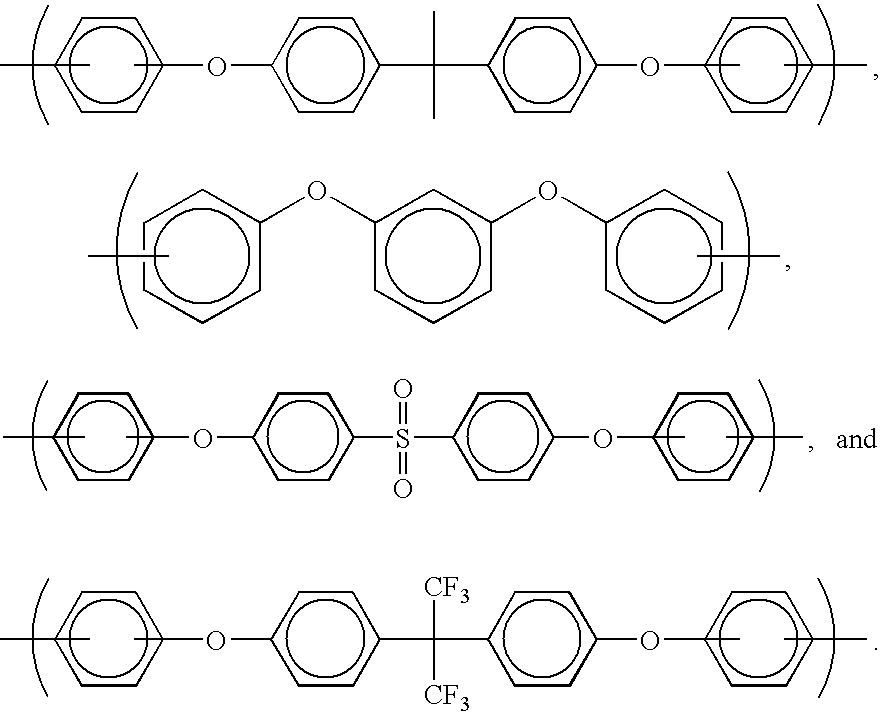
- R is selected from the group consisting of
-

-
- wherein R1 is selected from the group consisting of alkyl-substituted phenyls,
-

- X is selected from the group consisting of pheiiyl sulfones, aromatics, aliphatics, and cyclic aliphatics; and
-

- where Z is selected from the group consisting of siloxanes and moieties comprising ether bridges. The compound further comprises an endcap group derived from a compound selected from the group consisting of aromatic mono-amines, aliphatic mono-amines, cyclo-aliphatic mono-amines, and phthalic anhydrides.
-
FIG. 1 illustrates the inventive method of thinning and debonding two wafers according to the present invention; -
FIG. 2 is a flow diagram showing the typical process steps followed in the examples; and -
FIG. 3 is a graph depicting the rheological analysis results of a bonding composition according to the invention. - In more detail, the inventive compositions comprise a compound dispersed or dissolved in a solvent system. The compound can be a polymer or an oligomer and is preferably present in the composition at levels of from about 1% to about 70% by weight, more preferably from about 5% to about 50% by weight, and even more preferably from about 15% to about 40% by weight, based upon the total weight of solids in the composition taken as 100% by weight.
- The preferred polymeric or oligomeric compounds are thermoplastic and preferably have a weight average molecular weight of from about 3,000 Daltons to about 300,000 Daltons, and more preferably from about 6,000 Daltons to about 50,000 Daltons. Preferred compounds preferably have a softening temperature (melt viscosity at 3,000 Pa·S) of at least about 150° C., more preferably at least about 200° C., and even more preferably from about 200° C. to about 250° C.
- Preferred compounds will be at least about 95%, preferably at least about 98%, and even more preferably about 100% by weight dissolved when allowed to sit at ambient temperatures in a solvent such as N-methyl-2-pyrrolidone, xylene, dimethylacetamide, N,N-dimethylformamide, dimethyl sulfoxide, and mixtures thereof, for a time period of about 1-24 hours.
- Some preferred compounds that work in the present invention include those selected from the group consisting of oligomers and polymers of imides, amideimides, amideimide-siloxanes, arid mixtures thereof.
- In one embodiment, preferred such compounds have the formula
-

- where R is selected from the group consisting of
-

- where R1 is selected from the group consisting of alkyl-substituted phenyls,
-

- Preferred alkyl-substituted phenyls for use in the present invention are phenyls substituted with C1 to C6 alkyls. Particularly preferred examples of alkyl-substituted phenyls are those selected from the group consisting of
-

- In formula (I) above, X is selected from the group consisting of phenyl sulfones, aromatics (preferably C6 to C60, more preferably C6 to C30, and even more preferably C6 to C24), aliphatics (preferably C2 to C15, more preferably C2 to C10, and even more preferably C2-C6), and cyclic aliphatics (preferably C4 to C60, more preferably C4 to C20, and even more preferably C4-C12).
- In one embodiment, X can be the above aromatic group, aliphatic group, or cyclic aliphatic group. In another embodiment, X can comprise aromatic groups with ether bridges (such as those discussed with respect to Z below) or aromatic groups with linkage groups and/or —NH2 groups at the meta position.
- Particularly preferred X groups are selected from the group consisting of alkyl substituted phlenyls (such as the ones discussed above), isopropylidenediphlenyl, and hexafluoroisopropylidene.
- In another embodiment, preferred such compounds have the formula
-

- where Z is selected from the group consisting of siloxanes and moieties comprising ether bridges. In embodiments where Z is a siloxane, preferred siloxanes have the formula
-

- where:
-
- each R3 is individually selected from the group consisting of hydrogen, alkyls (preferably C1 to C10, and more preferably C1-C2), and phenyls;
- m is 1 to 6; and
- p is 1 to 50, preferably 1 to 20, and more preferably 1 to 10.
- Preferred moieties comprising ether bridges are selected from the group consisting of
-

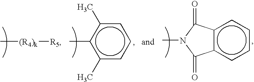
- In either the embodiment of Formula (I) or the embodiment of Formula (II), it is preferred that the polymer or oligomer further comprise an endcap group. Preferred endcap groups are derived from a compound selected from the group consisting of aromatic mono-amines, aliphatic mono-amines, cyclo-aliphatic monio-amines, and phthalic anhydrides. Particularly preferred endcap groups have a formula selected from the group consisting of alkyls (preferably C1 to C15, more preferably C1 to C10, and even more preferably C1-C6),
-

- where:
- R4 is an alkyl group (preferably C1 to C15, more preferably C1 to C10, and even more preferably C1-C6);
- R5 is a cyclic aliphatic group (preferably C3 to C12, and more preferably C5 to C6); and
- k is 0 to 20, preferably 0 to 10, and more preferably 0 to 5.
- The composition should comprise at least about 30% by weight solvent system, preferably from about 50% to about 90% by weight solvent system, more preferably from about 60% to about 90% by weight solvent system, and even more preferably from about 70% to about 90% by weight solvent system, based upon the total weight of the composition taken as 100% by weight. The solvent system should have a boiling point of from about 100-250° C., and preferably from about 120-220° C.
- Suitable solvents include those selected from the group consisting of N-methyl-2-pyrrolidone, xylene, dimethylacetaiiiide, N,N-dimethylformamide, dimethyl sulfoxide, and mixtures thereof.
- The total solids level in the composition should be at least about 10% by weight, preferably from about 10% to about 40% by weight, and more preferably from about 10% to about 30% by weight, based upon the total weight of the composition taken as 100% by weight.
- In other embodiments, the composition could include a number of optional ingredients, including surfactants, adhesion promoting agents, plasticizers, and/or antioxidants.
- When a surfactant is utilized, it is preferably present in the composition at a level of from about 0.1% to about 3% by weight, and more preferably from about 0.1% to about 1% by weight, based upon the total weight of the solids in the composition taken as 100% by weight. Examples of suitable surfactants include alcohol ethoxylates such as octyl phenol ethoxylate (sold wider the name Triton® X-100).
- When an adhesion promoting agent is utilized, it is preferably present in the composition at a level of from about 0.1% to about 3% by weight, and preferably from about 0.1% to about 1% by weight, based upon the total weight of the solids in the composition taken as 100% by weight. Examples of suitable adhesion promoting agent include those selected from the group consisting of bis(trimethoxysilylethyl)benzene, aminopropyl tri(alkoxy silanes) (e.g., aminopropyl tri(methoxy silane), aminopropyl tri(ethoxy silanes), -phenyl aminopropyl tri(ethoxy silane)), and other silane coupling agents.
- When an antioxidant is utilized, it is preferably present in the composition at a level of from about 0.01% to about 3% by weight, more preferably from about 0.01% to about 1.5% by weight, and even more preferably from about 0.01% to about 0.1% by weight, based upon the total weight of the solids in the composition taken as 100% by weight. Examples of suitable antioxidanlts include those selected from the group consisting of phenolic antioxidants (such as pentaerytliritol tetrakis(3-(3,5-ditert-butyl-4-hydroxyphenyl)propionate sold under the name Irganox® 1010 by Ciba) and phosphite antioxidants (such as tris(2,4-ditert-butylphenyl)phosphite sold under the name Irgafos® 168 by Ciba).
- The above ingredients can simply be mixed with the compound in the solvent system. The final composition should be thermoplastic (i.e., noncrosslinkable). Thus, the composition will be essentially free (less than about 0.1% by weight and preferably about 0% by weight) of crosslinking agents.
- The melt viscosity of the final composition will preferably be less than about 200 Pa·S, more preferably less than about 100 Pa·S, and even more preferably from about 10 Pa·S to about 50 Pa·S. For purposes of these measurements, the melt viscosity is determined via theological dynamic analysis (TA Instranents, AR-2000, two parallel-plate configuration where the plates have a diameter of 25 mm). Fruthermore, this melt viscosity is determined at 300-350° C. and there is preferably less than about 3% by weight, and more preferably less than about 2% by weight, loss of the composition. In other words, very little to no thermal decomposition occurs in the composition at this temperature, as determined by thermogravimetric analysis (TGA).
- Although the composition could be applied to either the carrier substrate or active wafer first, it is preferred that it be applied to the active wafer first. A preferred application method involves spin-coating the composition at spin speeds of from about 300-3,500 rpm (more preferably from about 500-1,500 rpm), at accelerations of from about 500-15,000 rpm/second, and for spin times of from about 30-300 seconds. It will be appreciated that the application steps can be varied to achieve a particular thickness.
- After coating, the substrate can be baked (e.g., on a hot plate) to evaporate the solvents. Typical baking would be at temperatures of from about 80-275° C., and preferably from about 150-225° C. for a time period of from about 2-15 minutes, and more preferably from about 3-10 minutes. The film thickness (on top of the topography) after bake will typically be at least about 5 μm, and more preferably from about 5-50 μm.
- After baking, the desired carrier wafer is contacted with, and pressed against, the layer of inventive composition. The carrier wafer is bonded to this inventive composition by heating at a temperature of from about 150-300° C., and preferably from about 180-300° C. This heating is preferably carried out under vacuum and for a time period of from about 1-10 minutes, under a bond force of from about 1 to about 15 kilonewtons.
-
FIG. 1( a) shows anexemplary stack 10 comprisingactive wafer 12 and carrier wafer orsubstrate 14.Active wafer 12 comprises aback surface 16 and anactive surface 18.Active surface 18 can comprise one or more active sites (not shown) as well as a plurality of topographical features (raised features or lines as well as holes, trenches, or spaces) such as, for example, those designated as 20 a-d.Feature 20 d represents the “highest” feature onactive surface 18. That is, the end portion orsurface 21 is further fromback surface 16 ofwafer 12 than the respective end portions of any other topographical feature onwafer 12. - Typical
active wafers 12 can include any microelectronic substrate. Examples of some possibleactive wafers 12 include those selected from the group consisting of microelectromechanical system (MEMS) devices, display devices, flexible substrates (e.g., cured epoxy substrates, roll-up substrates that can be used to form maps), compound semiconductors, low k dielectric layers, dielectric layers (e.g., silicon oxide, silicon nitride), ion implant layers, and substrates comprising silicon, aluminum, tungsten, tungsten silicide, gallium arsenide, germanium, tantalum, tantalum nitrite, SiGe, and mixtures of the foregoing. -
Carrier substrate 14 has abonding surface 22.Typical carrier substrates 14 comprise a material selected from the group consisting of sapphire, ceramic, glass, quartz, aluminum, silver, and silicon. -
Wafer 12 andcarrier substrate 14 are bonded together viabonding composition layer 24.Bonding layer 24 is formed of the polymer compositions described above, and has been applied and dried as also described above. As shown in theFIG. 1( a),bonding layer 24 is bonded toactive surface 18 ofwafer 12 as well as to bondingsurface 22 ofsubstrate 14. Unlike prior art tapes,bonding layer 24 is a uniform (chemically the same) material across its thickness. In other words, theentire bonding layer 24 is formed of the same composition. - It will be appreciated that, because
bonding layer 24 can be applied toactive surface 18 by spin-coating, the bonding composition flows into and over the various topographical features. Furthermore, thebonding layer 24 forms a uniform layer over the topography ofactive surface 18. To illustrate this point,FIG. 1 shows a plane designated by dashedline 26, atend portion 21 and substantially parallel to backsurface 16. The distance from this plane to bondingsurface 22 is represented by the thickness “T.” The thickness “T” will vary by less than about 8%, preferably by less than about 5%, more preferably by less than about 2%, and even more preferably by less than about 1% across the length ofplane 26 andsubstrate 14. - The wafer package can then be subjected to subsequent thinning (or other processing) of the substrate as shown in
FIG. 1( b), where 12′ presents thewafer 12 after thinning. It will be appreciated that the substrates can be thinned to thicknesses of less than about 100 μm, preferably less than about 50 μm, and more preferably less than about 25 μm. After thinning, typical backside processing, including photolitliography, via etching, and metallization, may be performed. - Advantageously, the dried layers of the inventive compositions possess a number of highly desirable properties. For example, the layers will exhibit low outgassing for vacuum etch processes. That is, if a 15-μm thick film of the composition is baked at 200° C. for 2 minutes, the solvents will be driven from the composition so that subsequent baking at 200° C. for 60 minutes results in a film thickness change of less than about 5%, preferably less than about 2%, and even more preferably less than about 1% or even 0% (referred to as the “Film Shrinkage Test”). Thus, the dried layers can be heated to temperatures of up to about 190° C., preferably up to about 200° C., more preferably up to about 220° C., and even more preferably tip to about 240° C. without physical changes or chemical reactions occurring in the layer. For example, the layers will not soften below these temperatures. In some embodiments, the layers can also be exposed to polar solvents (e.g., PGME) at a temperature of 85° C. for 90 minutes without reacting.
- The bond integrity of the dried layers can be maintained even upon exposure to an acid or base. That is, a dried layer of the composition having a thickness of about 15 μm can be submerged in an acidic media (e.g., concentrated sulfuric acid) or base (e.g., 30 wt. % KOH) at 85° C. for about 45 minutes while maintaining bond integrity. Bond integrity can be evaluated by using a glass carrier substrate and visually observing the bonding composition layer through the glass carrier substrate to check for bubbles, voids, etc. Also, bond integrity is maintained if the active wafer and carrier substrate cannot be separated by hand.
- After the desired processing has occurred, the active wafer or substrate can be separated from the carrier substrate by heating to temperatures of at least about 200° C., preferably at least about 225° C., and more preferably from about 250° C. to about 350° C. These temperature ranges represent the preferred softening points of the bonding composition layer. This heating will cause the bonding composition layer to soften and form softened
bonding composition layer 24′ as shown inFIG. 1( c), at which point the two substrates can be separated by sliding apart.FIG. 1( c) also shows anaxis 28, which passes through both ofwafer 12 andsubstrate 14, and the sliding forces would be applied in a direction generally transverse toaxis 28. Alternatively, sliding may not be necessary, and insteadwafer 12 orsubstrate 14 can be lifted upward (i.e., in a direction that is generally away from the other ofwafer 12 or substrate 14) to separate thewafer 12 from thesubstrate 14. - It will be appreciated that separation can be accomplished by simply sliding and/or lifting one of
wafer 12 orsubstrate 14 while maintaining the other in a substantially stationary position so as to resist the sliding or lifting force (e.g., by applying simultaneous opposing sliding forces towafer 12 and substrate 14). This Carl all be accomplished via conventional equipment. - Any bonding composition remaining in the device areas can be easily removed using the original solvent that was part of the composition prior to drying as well as using solvents such as xylene, NMP, and dimethyl sulfoxide. Any composition remaining behind will be completely dissolved (at least about 98%, preferably at least about 99%, and more preferably about 100%) after 5-15 minutes of exposure to the solvent. It is also acceptable to remove any remaining bonding composition using a plasma etch, either alone or in combination with a solvent removal process. After this step, a clean, bonding composition-
free wafer 12′ and carrier substrate 14 (not shown in their clean state) will remain. - The following examples set forth preferred methods in accordance with the invention. It is to be understood, however, that these examples are provided by way of illustration and nothing therein should be taken as a limitation upon the overall scope of the invention.
- In this procedure, 4,4′-bisphenol-A-dianhydride (BPADA, 57.25 grams, 0.011 moles), m-phenylene diamine (10.81 grams, 0.01 mol), and 2.6-dimethyl aniline (2.42 grams, 0.02 mol) were dissolved in N-methyl-2-pyrrolidone up to a final concentration of 15 wt. % of BPADA. The solution was allowed to stir at room temperature under an inert atmosphere for 12 hours. Xylene (38.17 grams) was added to the resulting amic acid solution to form an azeotropic solution to remove water during imidization, carried out by heating the solution to 180° C. for an additional 12 hours. The resulting imide solution was spin coated at 1,500 rpm for 60 seconds to form void-free, homogeneous films.
-

- In this Example, 4,4′-bisphenol-A-dianhydride (57.25 grams, 0.011 moles), m-phenylene diamine (10.81 grams, 0.01 mol), and n-butyl amine (1.46 grams, 0.02 mol) were dissolved in N-methyl-2-pyrrolidonie up to a final concentration of 15 wt. % of BPADA. The solution was allowed to stir at room temperature under an inert atmosphere for 12 hours. After this stage, the resulting poly(amic-acid) solution, with added xylene (38.17 grams), was imidized upon heating to 180° C. under a nitrogen purge for additional 12 hours.
-

- For this procedure, 4,4′-Bisphenol-A-dianhydride (57.25 grams, 0.011 moles), O-Tolidinie (21.229 grams, 0.01 mol), and 2.6-dimethyl aniline (2.42 grams, 0.02 mol) were dissolved in N-methyl-2-pyrrolidone up to a final concentration of 15 wt % of BPADA. The solution was allowed to stir at room temperature under an inert atmosphere for 12 hours. Xylene (38.17 grams) was added to the resulting amic acid solution to form an azeotropic solution to remove water during imidization, carried out by heating the solution to 180° C. for an additional 12 hours. The resulting imide solution was spin coated at appropriate speed to form void-free, homogeneous films.
-

- In this example, 4,4′-bisphenol-A-dianhydride (57.25 grams, 0.011 moles), m-phenylene diamine (7.57 grams, 0.007 mol), 2-methyl-1,5-pentanediamine (0.348 grams, 0.003 mol, commercially available from Invista under trade name of DYTEK-A), and 2.6-dimethyl aniline (2.42 grams, 0.02 mol) were dissolved in N-methyl-2-pyrrolidone up to a final concentration of 15 wt. % of BPADA. The solution was allowed to stir at room temperature under an inert atmosphere for 12 hours. Xylene (38.17 grams) was added to the resulting amic acid solution to form an azeotropic solution to remove water during imidization, carried out by heating the solution to 180° C. for an additional 12 hours. The resulting imide solution was spin coated at appropriate speed to form void-free, homogeneous films.
-

- In this procedure, trimellitic anlhydride chloride (0.447 grams, 2.12 mmol), 2,2-bis[4-(4-aminophenoxy) phenyl] propane (2.0 grams, 4.87 mmol), and triethylamnine (0.257 grams, 2.54 mmol) were dissolved in N-methyl-2-pyrrolidone at 0-5° C. to a concentration of 15 wt. % of the total amount of all monomers. The solution was allowed to stir at 0-5° C. under an inert atmosphere for 2 hours. Next, 4,4′-bisphenol-A-dianhydride (1.105 grams, 2.12 mmol), phthalic anhydride (0.199 grams, 1.34 mmol), and additional N-methyl-2-pyrrolidone were added to a final concentration of 15 wt. %. The solution was stirred at room temperature under an inert atmosphere for 20 hours. The resulting precipitate (triethylamine chloride) was filtered, and xylene (2.5 grams) was added to the amic-acid solution to form an azeotropic solution to remove water during imidization, which was carried out by heating the solution to 180° C. for an additional 12 hours. The structure of the polymer is shown below. The resulting amide-imide solution was spin coated at appropriate speed to form void-free, homogeneous films.
-

- In this Example, trimellitic anhydride chloride (1.0 grams, 4.7 mmol), 2,2-Bis[4-(4-aminophenoxy) phenyl] propane (2.464 grams, 6.0 mmol), and triethylamine (0.571 grams, 5.64 mmol) were dissolved in N-methyl-2-pyrrolidone at 0-5° C. to a concentration of 15 wt. %. The solution was allowed to stir at 0-5° C. under an inert atmosphere for 1 hour. Phthalic anhydride (0.439 grams, 2.96 mmol) and additional N-methyl-2-pyrrolidone were added to a final concentration of 15 wt. %. The solution was stirred at room temperature under an inert atmosphere for 20 hours. The resulting precipitate (triethylamine chloride) was filtered, and xylene (2.6 grams) was added to the amic-acid solution to form an azeotropic solution to remove water during imidization, which was carried out by heating the solution to 180° C. for additional 12 hours. The resulting amide-imide solution was spin coated at appropriate speed to form void-free, homogeneous films.
-

- In this procedure, trimellitic anhydride chloride (0.69 grams, 3.28 mmol), 1,3-Bis(3-aminophenoxy) benzene (Commercially available from CHRISKEV Company, Inc. under trade name of APB-133, 1.0 grams, 3.42 mmol), and triethylamine (0.398 grams, 3.93 mmol) were dissolved in N-methyl-2-pyrrolidone at 0-5° C. to a concentration of 15 wt. %. The solution was allowed to stir at 0-5° C. under an inert atmosphere for 1 hour. Phthalic anhydride (0.0427 grams, 0.29 mmol) and additional N-methyl-2-pyrrolidone were added to a final concentration of 15 wt. %. The solution was stirred at room temperature under an inert atmosphere for 20 hours. The resulting precipitate (triethylamine chloride) was filtered, and xylene (1.29 grams) was added to the amic-acid solution to form an azeotropic solution to remove water during imidization, carried out by heating the solution to 180° C. for an additional 12 hours. The resulting amide-imide solution was spin coated at appropriate speed to form void-free, homogeneous films.
-

- In this procedure, trimellitic anhydride chloride (1.149 grams, 5.46 mmol), 1,3-bis(3-aminopropyl) tetramethyl disiloxane (0.226 grams, 0.91 mmol), and triethylamine (0.663 grams, 6.55 mmol) were dissolved in N-methyl-2-pyrrolidone/THF cosolvent (70/30 vol) at 0-5° C. to a concentration of 15 wt. %. The solution was allowed to stir at 0-5° C. under an inert atmosphere for 12 hours. Next, 2,2-Bis[4-(4-aminophenoxy) phenyl] propane (2.0 grams, 4.87 mmol), phthalic anhydride (0.108 grams, 0.729 mmol), and additional N-methyl-2-pyrrolidone were added to a final concentration of 15 wt. %. The solution was stirred at room temperature under an inert atmosphere for 12 hours. The resulting precipitate (triethylamine chloride) was filtered, and xylene (2.3 grams) was added to the amic-acid solution to form an azeotropic solution to remove water during imidization, which was carried out by heating the solution to 180° C. for an additional 12 hours. The resulting amide-imide-siloxanie solution was spin coated at 1,500 rpm for 60 seconds to forn void-free, homogeneous films.
-

- In this procedure, trimellitic aiihydride chloride (0.372 grams, 1.77 mmol), 1,3-bis(3-aminopropyl) tetramethyl disiloxane (0.220 grams, 0.89 mmol), and triethylamine (0.215 grams, 2.12 mmol) were dissolved in N-methyl-2-pyrrolidone/THF cosolvent (70/30 vol) at 0-5° C. to a concentration of 15 wt. %. The solution was allowed to stir at 0-5° C. under an inert atmosphere for 12 hours. Next, 2,2-Bis[4-(4-aminophenoxy) phenyl] propane (2.0 grams, 4.87 mmol), 4,4′-Bisphenol-A-dianhydride (1.840 grams, 3.54 mmol), phthalic anhydride (0.141 grams, 0.95 mmol), and additional N-methyl-2-pyrrolidone were added to a final concentration of 15 wt. %. The solution was stirred at room temperature under an inert atmosphere for 12 hours. The resulting precipitate (triethylamine chloride) was filtered, and xylene (3.0 grams) was added to the amic-acid solution to form an azeotropic solution to remove water during imidization, which was carried out by heating the solution to 180° C. for an additional 12 hours. The resulting amide-imide-siloxaine solution was spin coated at 1,500 rpm for 60 seconds to form void-free, homogeneous films.
-

- In this Example, trimellitic anhydride chloride (1.080 grams, 5.13 mmol), aminopropyl terminated polydimethylsiloxane (commercially available from Gelest, Inc., 0.420 grams, 0.47 nimol), and triethylamine (0.623 grams, 6.15 mmol) were dissolved in N-methyl-2-pyrrolidone/THF cosolvent (70/30 vol) at 0-5° C. to a concentration of 15 wt. %. The solution was allowed to stir at 0-5° C. under an inert atmosphere for 12 hours. Next, 2,2-Bis[4-(4-aminophenoxy) phenyl] propane (2.0 grams, 4.87 mmol), phthalic anhydride (0.063 grams, 0.425 mmol), and additional N-methyl-2-pyrrolidone were added to a final concentration of 15 wt. %. The solution was stirred at room temperature under an inert atmosphere for 12 hours. The resulting precipitate (triethylamine chloride) was filtered, and xylene (2.4 grams) was added to the amic-acid solution to form an azeotropic solution to remove water during imidization, which was carried out by heating the solution to 180° C. for additional 12 hours. The resulting amide-imide-siloxanie solution was spin coated at 1,500 rpm for 60 seconds to form void-free, homogeneous films.
-

- The formulations from Examples 1 through 10 were spin-coated onto various substrate wafers. After baking to evaporate the solvent, a second wafer was bonded to each coated wafer by applying pressure. The typical procedure for temporary wafer bonding using these adhesives is shown in
FIG. 2 . The bonded wafers were tested for mechanical strength, thermal stability, and chemical resistance. The wafers were tested for de-bonding by manually sliding them apart at acceptable temperatures. - The viscosity, softening point, and Tg of the compositions of Examples 1 and 3 are reported in Table 1, and all these materials were successfully tested for de-bonding. Further studies on thermal stability and chemical resistance were carried out on these four compositions. All of these compositions possessed the required thermal stability of at least up to 350° C. and exhibited minimal out-gassing (<0.5 wt. %).
-
TABLE 1 Properties of Examples 1 and 3 VIS- Softening COSITY Temperature Molecular EXAM- (Pa · S, (in ° C. at Weight Tg PLE 350° C.) 3,000 Pa · S) (Mw, Daltons) (° C.) 1 50 210 10,800 161 3 15 210 6,100 152 - The compositions of the amideimide polymers from Examples 5-7 have aromatic amines that have ether or alkane linkages. As a result, the materials have low softening points, glass transition temperatures, and melt viscosities. The rheology data of the example materials are shown in
FIG. 3 . The viscosity, softening point, and Tg of the examples are reported in Table 2, and all these materials have been successfully tested for de-bonding. Further studies on thermal stability and chemical resistance have been carried out on these compositions. All of these compositions possess the required thermal stability at least up to 350° C. and exhibit minimal out-gassing (<0.5 wt. %). -
TABLE 2 Properties of Examples 5-7 VIS- Softening Weight Loss Molecular COSITY Temperature (Isothermal Weight EXAM- (Pa · S, (in ° C. at at 350° C. (Mn, Tg PLE 350° C.) 3,000 Pa · S) for 4 hrs) Daltons) (° C.) 5 20 253 1.337% 6,000 173 6 112 282 1.561% 3,000 195 7 37 255 2.218% 6,000 163 - The compositions of the amideimide-siloxane polymers from Examples 8-10 include siloxane units that are capped by amide groups, which form hydrogen bonding inter- and intra-molecularly. As a result, the siloxane units are isolated from phase change and prevented from introducing phase separation. This effect is shown below. The viscosities, softening points, and Tg of the examples are reported in Table 3, and all of these materials were successfully tested for de-bonding. Further studies on thermal stability and chemical resistance have been carried out on these compositions. All of these compositions possess the required thermal stability at least up to 350° C. and exhibit minimal out-gassing (<0.5 wt. %).
-

-
TABLE 3 Properties of Examples 8-10 VIS- Softening Weight Loss Molecular COSITY Temperature (Isothermal Weight EXAM- (Pa · S, (in ° C. at at 350° C. (Mn, Tg PLE 350° C.) 3,000 Pa · S) for 4 hrs) Daltons) (° C.) 8 44 260 4.085% 10,000 197 9 67 253 1.407% 10,000 150 10 1017 312 2.293% 16,000 150 - Trimellitic anhydride chloride (2.245 grams, 10.66 mmol),2,2-Bis[4-(3-aminophenoxy) phenyl] sulfone (10.0 grams, 23.12 mmol), and triethylamine (1.294 grams, 12.79 mmol) were dissolved in N-methyl-2-pyrrolidone at 0-5° C. to a concentration of 15 wt. %. The solution was allowed to stir at 0-5° C. under an inert atmosphere for 1 hour. Bisphenol-A-dianhydride (5.550 grams, 10.66 mmol), phthalic anhydride (0.555 grams, 3.74 mmol), and additional N-methyl-2-pyrrolidonle were added to a final concentration of 15 wt. %. The solution was stirred at room temperature under an inert atmosphere for 20 hours. The resulting precipitate (triethylaminie chloride) was filtered, and xylene (6.2 grams) was added to the amic-acid solution to form an azeotropic solution to remove water during imidization, carried out by heating the solution to 180° C. for an additional 12 hours. The resulting amide-imide solution was spin coated at 1,500 rpm for 60 seconds to form void-free, homogeneous films.
-

- In this procedure, 4,4′-Bisphenol-A-dianhydride (10.624 grams, 20.40 mmol), 2,2-Bis[4-(4-aminophenoxy) phenyl] sulfone (8.0 grams, 18.5 mmol), and cyclohexylamiine (0.399 grams, 4.0 mmiol) were dissolved in N-methyl-2-pyrrolidone up to a final concentration of 10 wt. %. The solution was allowed to stir at room temperature under an inert atmosphere for 12 hours. Xylene (12.0 grams) was added to the resulting amic-acid solution in order to form an azeotropic solution to remove water during imidization, which was carried out by heating the solution to 180° C. for additional 12 hours. The resulting imide solutions were spill coated at 1,500 rpm at 60 seconds to form void free homogeneous films.
-

- In this Example, 4,4′-Bisphenol-A-dianhydride (20.0 grams, 38.43 mmol), 2,4,6-trimethyl-m-pheniylene diamine (0.811 grams, 5.40 mmol), 2-Methyl-1,5-Pentanediamine (commercially available from Invista under trade name of Dytek-A, 3.556 grams, 30.60 mmol), and 2.6-dimethyl aniline (0.609 grams, 5.03 mmol) were dissolved in N-methyl-2-pyrrolidone up to a final concentration of 10 wt. %. The solution was allowed to stir at room temperature under an inert atmosphere for 12 hours. Xylene (16.6 grams) was added to the resulting amic-acid solution in order to form an azeotropic solution to remove water during imidization, which was carried out by heating the solution to 180° C. for an additional 12 hours. The resulting imide solutions were spin coated at 1,500 rpm at 60 seconds to form void-free, homogeneous films.
-

- In this procedure, 4,4′-Bisphenol-A-dianhydride (10.0 grams, 19.2 mmol), 3,3′-diaminodiphenyl sulfone (2.220 grams, 8.9 mmol), 2-Methyl-1,5-Pentanediamine (commercially available from Invista under trade name of Dytek-A, 1.039 grams, 8.9 mmol), and cyclohexylamine (0.273 grams, 2.8 mol) were dissolved in N-methyl-2-pyrrolidone up to a final concentration of 10 wt. %. The solution was allowed to stir at room temperature under an inert atmosphere for 12 hours. Xylene (9.0 grams) was added to the resulting amic-acid solution in order to form an azeotropic solution to remove water during imidization, carried out by heating the solution to 180° C. for additional 12 hours. The resulting imide solutions were spin coated at 1,500 rpm at 60 seconds to form void-free, homogeneous films.
-

- In this Example, 4,4′-Bisphenol-A-dianhydride (10.0 grams, 19.2 mmol), 2,4,6-trimethyl-m-phlenylenediamine (0.663 grams, 4.42 mmol), 1,2-diaminocyclohexwie (1.514 grams, 13.26 mmol), and cyclohexylamine (0.317 grams, 3.2 mmol) were dissolved in N-methyl-2-pyrrolidone up to a final concentration of 10 wt. %. The solution was allowed to stir at room temperature under an inert atmosphere for 12 hours. Xylene (8.3 grams) was added to the resulting amic-acid solution in order to form all azeotropic soltition to remove water during imidization, carried out by heating the solution to 180° C. for an additional 12 hours. The resulting imide solutions were spin coated at 1,500 rpm for 60 seconds to form void-free, homogeneous films.
-

- In this procedure, 4,4′-Bisphenol-A-dianhydride (10.0 grams, 19.2 mmol), 2,4,6-trimethyl-m-phenylenediamine (0.657 grams, 4.38 mmol), 4,4′-methylene-bis-cyclolhexylamine (2.762 grams, 13.13 mmol), and cyclohexylamine (0.355 grams, 3.58 mmol) were dissolved in N-methyl-2-pyrrolidone up to a final concentration of 10 wt. %. The solution was allowed to stir at room temperature under an inert atmosphere for 12 hours. Xylene (9.2 grams) was added to the resulting amic-acid solution in order to form an azeotropic solution to remove water during imidization, which was carried out by heating the solution to 180° C. for an additional 12 hours. The resulting imide solutions were spin coated at 1,500 rpm for 60 seconds to form void-free, homogeneous films.
-

- The viscosity, softening point, and Tg, of the compositions of Examples 15, 16, 19, and 20 are reported in Table 4, while the values of the compositions of Examples 17-18 are reported in Table 5. Further studies on thermal stability and chemical resistance were carried out on these compositions. All of these compositions possessed the required thermal stability of at least up to 350° C. and exhibited minimal out-gassing (<0.5 wt. %).
-
TABLE 4 Properties of Examples 15-16 and 19-20 VIS- Softening Weight Loss Molecular COSITY Temperature (Isothermal Weight EXAM- (Pa · S, (in ° C. at at 350° C. (Mn, Tg PLE 350° C.) 3,000 Pa · S) for 4 hrs) Daltons) (° C.) 15 4.943 240 1.420% 3,940 176 16 169.6 299 0.1740% 19,800 207 19 0.796 239 3.173% 4,780 185 20 29.47 273 0.866% 9,810 202 -
TABLE 5 Properties of Examples 17-18 VIS- Softening Weight Loss Molecular COSITY Temperature (Isothermal Weight EXAM- (Pa · S, (in ° C. at at 350° C. (Mn, Tg PLE 350° C.) 3,000 Pa · S) for 4 hrs) Daltons) (° C.) 17 22.52 214 0.6721% 12,700 144 18 4.451 208 1.557% 5,870 150
Claims (40)


Priority Applications (3)
| Application Number | Priority Date | Filing Date | Title |
|---|---|---|---|
| US12/146,148 US7935780B2 (en) | 2007-06-25 | 2008-06-25 | High-temperature spin-on temporary bonding compositions |
| TW097123665A TWI418602B (en) | 2007-06-25 | 2008-06-25 | High-temperature spin-on temporary bonding compositions |
| US12/949,019 US8236669B2 (en) | 2007-06-25 | 2010-11-18 | High-temperature spin-on temporary bonding compositions |
Applications Claiming Priority (2)
| Application Number | Priority Date | Filing Date | Title |
|---|---|---|---|
| US94607707P | 2007-06-25 | 2007-06-25 | |
| US12/146,148 US7935780B2 (en) | 2007-06-25 | 2008-06-25 | High-temperature spin-on temporary bonding compositions |
Related Child Applications (1)
| Application Number | Title | Priority Date | Filing Date |
|---|---|---|---|
| US12/949,019 Division US8236669B2 (en) | 2007-06-25 | 2010-11-18 | High-temperature spin-on temporary bonding compositions |
Publications (2)
| Publication Number | Publication Date |
|---|---|
| US20090038750A1 true US20090038750A1 (en) | 2009-02-12 |
| US7935780B2 US7935780B2 (en) | 2011-05-03 |
Family
ID=40186272
Family Applications (2)
| Application Number | Title | Priority Date | Filing Date |
|---|---|---|---|
| US12/146,148 Active 2028-07-21 US7935780B2 (en) | 2007-06-25 | 2008-06-25 | High-temperature spin-on temporary bonding compositions |
| US12/949,019 Active 2028-08-22 US8236669B2 (en) | 2007-06-25 | 2010-11-18 | High-temperature spin-on temporary bonding compositions |
Family Applications After (1)
| Application Number | Title | Priority Date | Filing Date |
|---|---|---|---|
| US12/949,019 Active 2028-08-22 US8236669B2 (en) | 2007-06-25 | 2010-11-18 | High-temperature spin-on temporary bonding compositions |
Country Status (6)
| Country | Link |
|---|---|
| US (2) | US7935780B2 (en) |
| JP (1) | JP5788173B2 (en) |
| KR (1) | KR101565176B1 (en) |
| CN (1) | CN101779268B (en) |
| TW (1) | TWI418602B (en) |
| WO (1) | WO2009003029A2 (en) |
Cited By (17)
| Publication number | Priority date | Publication date | Assignee | Title |
|---|---|---|---|---|
| US20100263794A1 (en) * | 2009-04-16 | 2010-10-21 | Suss Microtec Inc | Apparatus for mechanically debonding temporary bonded semiconductor wafers |
| US20110086955A1 (en) * | 2008-10-31 | 2011-04-14 | Brewer Science Inc. | Cyclic olefin compositions for temporary wafer bonding |
| US20110171478A1 (en) * | 2009-04-15 | 2011-07-14 | Brewer Science Inc. | Acid-etch resistant, protective coatings |
| US8236669B2 (en) | 2007-06-25 | 2012-08-07 | Brewer Science Inc. | High-temperature spin-on temporary bonding compositions |
| US8366873B2 (en) | 2010-04-15 | 2013-02-05 | Suss Microtec Lithography, Gmbh | Debonding equipment and methods for debonding temporary bonded wafers |
| US20130089967A1 (en) * | 2011-10-07 | 2013-04-11 | Shin-Etsu Chemical Co., Ltd. | Temporary adhesive composition and method for manufacturing thin wafer using the same |
| EP2733734A2 (en) | 2010-08-06 | 2014-05-21 | Brewer Science, Inc. | Multiple bonding layers for thin-wafer handling |
| US9064686B2 (en) | 2010-04-15 | 2015-06-23 | Suss Microtec Lithography, Gmbh | Method and apparatus for temporary bonding of ultra thin wafers |
| US9127126B2 (en) | 2012-04-30 | 2015-09-08 | Brewer Science Inc. | Development of high-viscosity bonding layer through in-situ polymer chain extension |
| US9349643B2 (en) | 2013-04-01 | 2016-05-24 | Brewer Science Inc. | Apparatus and method for thin wafer transfer |
| US9472437B2 (en) | 2009-04-16 | 2016-10-18 | Suss Microtec Lithography Gmbh | Debonding temporarily bonded semiconductor wafers |
| GB2544563A (en) * | 2015-11-20 | 2017-05-24 | Rfhic Corp | Mounting of semiconductor-on-diamond wafers for device processing |
| US9837295B2 (en) | 2010-04-15 | 2017-12-05 | Suss Microtec Lithography Gmbh | Apparatus and method for semiconductor wafer leveling, force balancing and contact sensing |
| US9859141B2 (en) | 2010-04-15 | 2018-01-02 | Suss Microtec Lithography Gmbh | Apparatus and method for aligning and centering wafers |
| US10103048B2 (en) | 2013-08-28 | 2018-10-16 | Brewer Science, Inc. | Dual-layer bonding material process for temporary bonding of microelectronic substrates to carrier substrates |
| US20190091979A1 (en) * | 2014-12-03 | 2019-03-28 | Tokyo Ohka Kogyo Co., Ltd. | Laminate production method, substrate processing method, and laminate |
| US11610801B2 (en) | 2019-01-22 | 2023-03-21 | Brewer Science, Inc. | Laser-releasable bonding materials for 3-D IC applications |
Families Citing this family (69)
| Publication number | Priority date | Publication date | Assignee | Title |
|---|---|---|---|---|
| US8673163B2 (en) | 2008-06-27 | 2014-03-18 | Apple Inc. | Method for fabricating thin sheets of glass |
| US7810355B2 (en) | 2008-06-30 | 2010-10-12 | Apple Inc. | Full perimeter chemical strengthening of substrates |
| US9063605B2 (en) | 2009-01-09 | 2015-06-23 | Apple Inc. | Thin glass processing using a carrier |
| US7918019B2 (en) | 2009-01-09 | 2011-04-05 | Apple Inc. | Method for fabricating thin touch sensor panels |
| EP2404228B1 (en) | 2009-03-02 | 2020-01-15 | Apple Inc. | Techniques for strengthening glass covers for portable electronic devices |
| US9778685B2 (en) | 2011-05-04 | 2017-10-03 | Apple Inc. | Housing for portable electronic device with reduced border region |
| KR20120132624A (en) * | 2010-02-12 | 2012-12-06 | 다우 코닝 코포레이션 | Temporary wafer bonding method for semiconductor processing |
| US9213451B2 (en) | 2010-06-04 | 2015-12-15 | Apple Inc. | Thin glass for touch panel sensors and methods therefor |
| US10189743B2 (en) | 2010-08-18 | 2019-01-29 | Apple Inc. | Enhanced strengthening of glass |
| US8824140B2 (en) | 2010-09-17 | 2014-09-02 | Apple Inc. | Glass enclosure |
| US8950215B2 (en) | 2010-10-06 | 2015-02-10 | Apple Inc. | Non-contact polishing techniques for reducing roughness on glass surfaces |
| TW201241134A (en) * | 2010-12-14 | 2012-10-16 | Sumitomo Bakelite Co | Method of processing a base material |
| WO2012092447A1 (en) | 2010-12-29 | 2012-07-05 | Promerus, Llc | Polymer compositions for temporary bonding |
| US10781135B2 (en) | 2011-03-16 | 2020-09-22 | Apple Inc. | Strengthening variable thickness glass |
| US9725359B2 (en) | 2011-03-16 | 2017-08-08 | Apple Inc. | Electronic device having selectively strengthened glass |
| JP5729097B2 (en) * | 2011-04-07 | 2015-06-03 | Jsr株式会社 | Substrate processing method, temporary fixing material and electronic component |
| US9128666B2 (en) | 2011-05-04 | 2015-09-08 | Apple Inc. | Housing for portable electronic device with reduced border region |
| KR101287186B1 (en) * | 2011-05-13 | 2013-07-23 | (주)태인케미컬 | Optical High Transparent Adhesive Sheet and Method for Separating Display Panel Assembly |
| DE102011079687A1 (en) | 2011-07-22 | 2013-01-24 | Wacker Chemie Ag | Temporary bonding of chemically similar substrates |
| US8940104B2 (en) | 2011-08-02 | 2015-01-27 | Brewer Science Inc. | Cleaning composition for temporary wafer bonding materials |
| US9944554B2 (en) | 2011-09-15 | 2018-04-17 | Apple Inc. | Perforated mother sheet for partial edge chemical strengthening and method therefor |
| FR2980204B1 (en) * | 2011-09-20 | 2015-03-27 | Rhodia Operations | NOVEL (CO) THERMOPLASTIC POLYIMIDES AND METHODS OF SYNTHESIS |
| FR2980201B1 (en) * | 2011-09-20 | 2014-10-24 | Rhodia Operations | THERMOPLASTIC POLYIMIDES |
| US9516149B2 (en) | 2011-09-29 | 2016-12-06 | Apple Inc. | Multi-layer transparent structures for electronic device housings |
| NL2007705C2 (en) * | 2011-11-02 | 2013-05-21 | Stichting Energie | Low cost polymer supported hybrid silica membrane and production thereof. |
| US10144669B2 (en) | 2011-11-21 | 2018-12-04 | Apple Inc. | Self-optimizing chemical strengthening bath for glass |
| US9390949B2 (en) * | 2011-11-29 | 2016-07-12 | Taiwan Semiconductor Manufacturing Company, Ltd. | Wafer debonding and cleaning apparatus and method of use |
| US10381254B2 (en) | 2011-11-29 | 2019-08-13 | Taiwan Semiconductor Manufacturing Co., Ltd. | Wafer debonding and cleaning apparatus and method |
| US11264262B2 (en) | 2011-11-29 | 2022-03-01 | Taiwan Semiconductor Manufacturing Company, Ltd. | Wafer debonding and cleaning apparatus |
| US10133156B2 (en) | 2012-01-10 | 2018-11-20 | Apple Inc. | Fused opaque and clear glass for camera or display window |
| US8773848B2 (en) | 2012-01-25 | 2014-07-08 | Apple Inc. | Fused glass device housings |
| US10543662B2 (en) | 2012-02-08 | 2020-01-28 | Corning Incorporated | Device modified substrate article and methods for making |
| WO2015157202A1 (en) | 2014-04-09 | 2015-10-15 | Corning Incorporated | Device modified substrate article and methods for making |
| US9946302B2 (en) | 2012-09-19 | 2018-04-17 | Apple Inc. | Exposed glass article with inner recessed area for portable electronic device housing |
| US9269623B2 (en) | 2012-10-25 | 2016-02-23 | Rohm And Haas Electronic Materials Llc | Ephemeral bonding |
| DE102012220954A1 (en) | 2012-11-16 | 2014-05-22 | Wacker Chemie Ag | Sandable silicone elastomer composition and use thereof |
| TWI617437B (en) | 2012-12-13 | 2018-03-11 | 康寧公司 | Facilitated processing for controlling bonding between sheet and carrier |
| US10014177B2 (en) | 2012-12-13 | 2018-07-03 | Corning Incorporated | Methods for processing electronic devices |
| US9340443B2 (en) | 2012-12-13 | 2016-05-17 | Corning Incorporated | Bulk annealing of glass sheets |
| US10086584B2 (en) | 2012-12-13 | 2018-10-02 | Corning Incorporated | Glass articles and methods for controlled bonding of glass sheets with carriers |
| US9269603B2 (en) | 2013-05-09 | 2016-02-23 | Globalfoundries Inc. | Temporary liquid thermal interface material for surface tension adhesion and thermal control |
| US9459661B2 (en) | 2013-06-19 | 2016-10-04 | Apple Inc. | Camouflaged openings in electronic device housings |
| US8962449B1 (en) | 2013-07-30 | 2015-02-24 | Micron Technology, Inc. | Methods for processing semiconductor devices |
| EP3051574A4 (en) | 2013-09-25 | 2017-05-10 | Shibaura Mechatronics Corporation | Substrate treatment device, method for separating bonded substrate, and method for removing adhseive |
| US10510576B2 (en) | 2013-10-14 | 2019-12-17 | Corning Incorporated | Carrier-bonding methods and articles for semiconductor and interposer processing |
| US9315696B2 (en) | 2013-10-31 | 2016-04-19 | Dow Global Technologies Llc | Ephemeral bonding |
| SG11201605469PA (en) | 2014-01-07 | 2016-08-30 | Brewer Science Inc | Cyclic olefin polymer compositions and polysiloxane release layers for use in temporary wafer bonding processes |
| US9865490B2 (en) | 2014-01-07 | 2018-01-09 | Brewer Science Inc. | Cyclic olefin polymer compositions and polysiloxane release layers for use in temporary wafer bonding processes |
| KR102353030B1 (en) | 2014-01-27 | 2022-01-19 | 코닝 인코포레이티드 | Articles and methods for controlled bonding of thin sheets with carriers |
| US9355881B2 (en) | 2014-02-18 | 2016-05-31 | Infineon Technologies Ag | Semiconductor device including a dielectric material |
| US9886062B2 (en) | 2014-02-28 | 2018-02-06 | Apple Inc. | Exposed glass article with enhanced stiffness for portable electronic device housing |
| TWI661935B (en) * | 2014-06-13 | 2019-06-11 | 日商富士軟片股份有限公司 | Laminated body temporarily, manufacturing method of laminated body temporarily, and laminated body with element wafer |
| KR102404034B1 (en) | 2014-07-22 | 2022-05-31 | 브레우어 사이언스, 인코포레이션 | Polyimides as laser release materials for 3-d ic applications |
| US9644118B2 (en) | 2015-03-03 | 2017-05-09 | Dow Global Technologies Llc | Method of releasably attaching a semiconductor substrate to a carrier |
| CN107635769B (en) | 2015-05-19 | 2020-09-15 | 康宁股份有限公司 | Article and method for bonding sheet to carrier |
| EP3313799B1 (en) | 2015-06-26 | 2022-09-07 | Corning Incorporated | Methods and articles including a sheet and a carrier |
| TW201825623A (en) | 2016-08-30 | 2018-07-16 | 美商康寧公司 | Siloxane plasma polymers for sheet bonding |
| TWI821867B (en) | 2016-08-31 | 2023-11-11 | 美商康寧公司 | Articles of controllably bonded sheets and methods for making same |
| FR3060601B1 (en) * | 2016-12-20 | 2018-12-07 | Commissariat A L'energie Atomique Et Aux Energies Alternatives | ADHESIVE COMPOSITION AND ITS USE IN ELECTRONICS |
| CN107946283B (en) * | 2017-11-27 | 2020-03-17 | 华进半导体封装先导技术研发中心有限公司 | Wafer slide bonding structure and method for TSV exposure by using same |
| US11331692B2 (en) | 2017-12-15 | 2022-05-17 | Corning Incorporated | Methods for treating a substrate and method for making articles comprising bonded sheets |
| WO2019169394A1 (en) * | 2018-03-02 | 2019-09-06 | Kaneka Americas Holding, Inc. | Polyimides for temporary bonding adhesives, methods for manufacturing of thermoplastic polyimide materials, and methods for thin wafer bonding using the same |
| JP7267567B2 (en) * | 2018-10-31 | 2023-05-02 | ユニチカ株式会社 | Low dielectric constant polyimide |
| US11787978B2 (en) * | 2019-01-31 | 2023-10-17 | Synthomer Adhesive Technologies Llc | Product assembly adhesives comprising low volatile tackifier compositions |
| US20220049095A1 (en) * | 2020-08-14 | 2022-02-17 | Brewer Science, Inc. | Permanent bonding and patterning material |
| EP4317339A1 (en) | 2021-03-30 | 2024-02-07 | Nissan Chemical Corporation | Adhesive composition, laminate, method for manufacturing laminate, and method for manufacturing processed substrate |
| EP4310157A1 (en) | 2021-03-31 | 2024-01-24 | Nissan Chemical Corporation | Laminate, release agent composition, and method for manufacturing machined semiconductor substrate |
| KR20230164088A (en) | 2021-03-31 | 2023-12-01 | 닛산 가가쿠 가부시키가이샤 | Method for producing laminates, release agent compositions, and processed semiconductor substrates |
| KR20230165266A (en) | 2021-03-31 | 2023-12-05 | 닛산 가가쿠 가부시키가이샤 | Method for producing laminates, release agent compositions, and processed semiconductor substrates |
Citations (50)
| Publication number | Priority date | Publication date | Assignee | Title |
|---|---|---|---|---|
| US3234181A (en) * | 1961-03-15 | 1966-02-08 | Du Pont | Melt-fabricable end-capped aromatic polymides |
| US3392144A (en) * | 1967-05-15 | 1968-07-09 | Gen Electric | Polyamide compositions and polyimideamides therefrom |
| US3435002A (en) * | 1967-05-15 | 1969-03-25 | Gen Electric | Polyamide acid resins and polyimides therefrom |
| US3440204A (en) * | 1966-05-05 | 1969-04-22 | Gen Electric | Polyamide amide-acid coating solutions containing a silicone,method of using said solutions and surfaces coated therewith |
| US3553282A (en) * | 1969-09-08 | 1971-01-05 | Gen Electric | Siloxane containing polyamide acid blends |
| US3598784A (en) * | 1970-03-11 | 1971-08-10 | Gen Electric | Polysiloxane amides |
| US3598785A (en) * | 1970-03-11 | 1971-08-10 | Gen Electric | Polysiloxane amides |
| US3723385A (en) * | 1971-10-01 | 1973-03-27 | Gen Electric | Siloxane containing prepolymers and polyamide-imides prepared therefrom |
| US3740305A (en) * | 1971-10-01 | 1973-06-19 | Gen Electric | Composite materials bonded with siloxane containing polyimides |
| US3970494A (en) * | 1975-04-18 | 1976-07-20 | Western Electric Co., Inc. | Method for adhering one surface to another |
| US4281100A (en) * | 1979-05-09 | 1981-07-28 | General Electric Company | Injection moldable polyetherimide oligomers and method for making |
| US4331799A (en) * | 1980-01-10 | 1982-05-25 | General Electric Company | Copolymers of etherimides and amideimides |
| US4443591A (en) * | 1983-01-21 | 1984-04-17 | General Electric Company | Method for making polyetherimide |
| US4474942A (en) * | 1982-06-28 | 1984-10-02 | Takeda Chemical Industries, Ltd. | Cross-linked polyesteramide from bis(2-oxazoline) |
| US4480009A (en) * | 1980-12-15 | 1984-10-30 | M&T Chemicals Inc. | Siloxane-containing polymers |
| US4558114A (en) * | 1985-01-23 | 1985-12-10 | Ashland Oil, Inc. | Polymers derived from polyisocyanates, bicyclic amide acetals and oxazolines |
| US4599396A (en) * | 1984-09-04 | 1986-07-08 | General Electric Company | Crystalline polyetherimides and polyamic acid precursors therefor |
| US4710542A (en) * | 1986-05-16 | 1987-12-01 | American Cyanamid Company | Alkylcarbamylmethylated amino-triazine crosslinking agents and curable compositions containing the same |
| US4895972A (en) * | 1988-09-01 | 1990-01-23 | The United States Of American As Represented By The Administrator Of The National Aeronautics And Space Administration | Process for lowering the dielectric constant of polyimides using diamic acid additives |
| US4910288A (en) * | 1989-02-07 | 1990-03-20 | General Electric Company | Process for the preparation of polyetherimides |
| US4933132A (en) * | 1989-02-28 | 1990-06-12 | Hoechst Celanese Corp. | Process of making a shaped article from intermediate molecular weight polyimides |
| US4973651A (en) * | 1989-05-08 | 1990-11-27 | Hoechst Celanese Corp. | Polyimide polymers having 12-F fluorine-containing linking groups |
| US5043250A (en) * | 1990-07-17 | 1991-08-27 | Eastman Kodak Company | Radiation-sensitive composition containing a poly (N-acyl-alkyleneimine) and use thereof in lithographic printing plates |
| US5187228A (en) * | 1986-10-03 | 1993-02-16 | Dexter Corporation | Stabilizer for compatibilized polycarbonate and polyamide polymer blends |
| US5204399A (en) * | 1989-03-09 | 1993-04-20 | National Starch And Chemical Investment Holding Corporation | Thermoplastic film die attach adhesives |
| US5227461A (en) * | 1983-06-17 | 1993-07-13 | The Boeing Company | Extended difunctional end-cap monomers |
| US5773561A (en) * | 1996-08-02 | 1998-06-30 | International Business Machines Corporation | Polymer sealants/adhesives and use thereof in electronic package assembly |
| US5817744A (en) * | 1988-03-14 | 1998-10-06 | The Boeing Company | Phenylethynyl capped imides |
| US5844065A (en) * | 1997-05-14 | 1998-12-01 | National Science Council | 2,2'-dimethyl-4,4'-bis (4-aminophenoxy) biphenyl, and polymers prepared therefrom by polycondensation |
| US5886131A (en) * | 1997-05-30 | 1999-03-23 | China Textile Institute | Method for preparing 1,4-Bis(4-aminophenoxy)naphthalene and its polymers |
| US5939520A (en) * | 1997-09-05 | 1999-08-17 | Air Products And Chemicals, Inc. | Gas separation membranes based on regiospecific polyamide-imides |
| US6046072A (en) * | 1993-03-29 | 2000-04-04 | Hitachi Chemical Company, Ltd. | Process for fabricating a crack resistant resin encapsulated semiconductor chip package |
| US6054363A (en) * | 1996-11-15 | 2000-04-25 | Canon Kabushiki Kaisha | Method of manufacturing semiconductor article |
| US6066710A (en) * | 1998-10-29 | 2000-05-23 | Occidental Chemical Corporation | Imide-containing polymers made by bulk polymerization |
| US6110999A (en) * | 1998-03-06 | 2000-08-29 | Denovus Llc | Reusable adhesive composition and method of making the same |
| US6156820A (en) * | 1998-12-28 | 2000-12-05 | Occidental Chemical Corporation | Polyamideimidesiloxane hot melt adhesive |
| US6235818B1 (en) * | 1997-01-30 | 2001-05-22 | Mitsui Chemicals | Hot melt adhesive composition containing α-olefin/aromatic vinyl compound random copolymer |
| US6252010B1 (en) * | 1997-10-29 | 2001-06-26 | Hitachi Chemical Company, Ltd. | Siloxane-modified polyamideimide resin composition, adhesive film, adhesive sheet and semiconductor device |
| US20020115263A1 (en) * | 2001-02-16 | 2002-08-22 | Worth Thomas Michael | Method and related apparatus of processing a substrate |
| US20020127821A1 (en) * | 2000-12-28 | 2002-09-12 | Kazuyuki Ohya | Process for the production of thinned wafer |
| US6869894B2 (en) * | 2002-12-20 | 2005-03-22 | General Chemical Corporation | Spin-on adhesive for temporary wafer coating and mounting to support wafer thinning and backside processing |
| US20050070684A1 (en) * | 2003-09-26 | 2005-03-31 | General Electric Company | Polyimide sulfones, method and articles made therefrom |
| US6919422B2 (en) * | 2003-06-20 | 2005-07-19 | General Electric Company | Polyimide resin with reduced mold deposit |
| US20050164509A1 (en) * | 2004-01-28 | 2005-07-28 | Mitsui Chemicals, Inc. | Method of protecting semiconductor wafer and adhesive film for protection of semiconductor wafer |
| US20050173064A1 (en) * | 2003-12-01 | 2005-08-11 | Tokyo Ohka Kogyo Co., Ltd. | Substrate supporting plate and stripping method for supporting plate |
| US20060089487A1 (en) * | 2003-08-26 | 2006-04-27 | Norberto Silvi | Method of separating a polymer from a solvent |
| US7084201B2 (en) * | 2003-11-14 | 2006-08-01 | Wall-Guard Corporation Of Ohio | Non-flammable waterproofing composition |
| US20060183269A1 (en) * | 2003-07-28 | 2006-08-17 | Edward Fuergut | Method for producing a semiconductor component with a plastic housing and carrier plate for performing the method |
| US20070185310A1 (en) * | 2006-02-06 | 2007-08-09 | Moore John C | Thermal- and chemical-resistant acid protection coating material and spin-on thermoplastic adhesive |
| US20080200011A1 (en) * | 2006-10-06 | 2008-08-21 | Pillalamarri Sunil K | High-temperature, spin-on, bonding compositions for temporary wafer bonding using sliding approach |
Family Cites Families (48)
| Publication number | Priority date | Publication date | Assignee | Title |
|---|---|---|---|---|
| US3987122A (en) | 1972-04-03 | 1976-10-19 | Exxon Research And Engineering Company | Thermoplastic adhesive compositions |
| US3868433A (en) | 1972-04-03 | 1975-02-25 | Exxon Research Engineering Co | Thermoplastic adhesive compositions |
| US3959062A (en) | 1972-08-10 | 1976-05-25 | E. I. Du Pont De Nemours And Company | Method of joining surfaces using segmented copolyester adhesive |
| GB8320270D0 (en) | 1983-07-27 | 1983-09-01 | Raychem Ltd | Polymer composition |
| JPS61162525A (en) * | 1985-01-04 | 1986-07-23 | ゼネラル エレクトリツク カンパニイ | New copolyamideimide, its production and prepolymer thereof and its production |
| US4793337A (en) | 1986-11-17 | 1988-12-27 | E. R. Squibb & Sons, Inc. | Adhesive structure and products including same |
| JP2653401B2 (en) * | 1987-02-20 | 1997-09-17 | 日立化成工業 株式会社 | Method for producing polyamidoimide silicone polymer |
| NL8902683A (en) | 1989-10-31 | 1991-05-16 | Stamicarbon | MULTIPLE COMPONENT SYSTEM BASED ON OXAZOLINE AND A PHOSPHORUS CONTAINING COMPOUND. |
| JP2961642B2 (en) * | 1995-05-31 | 1999-10-12 | 株式会社巴川製紙所 | Adhesive tape and liquid adhesive for electronic parts |
| US5888650A (en) | 1996-06-03 | 1999-03-30 | Minnesota Mining And Manufacturing Company | Temperature-responsive adhesive article |
| SG67458A1 (en) * | 1996-12-18 | 1999-09-21 | Canon Kk | Process for producing semiconductor article |
| JP3347651B2 (en) * | 1997-09-17 | 2002-11-20 | 株式会社巴川製紙所 | Adhesive tape for electronic components |
| JP3688133B2 (en) * | 1998-09-25 | 2005-08-24 | 日立化成工業株式会社 | Heat resistant adhesive sheet for CSP substrate and method for producing CSP substrate using the same |
| JP3432409B2 (en) * | 1997-11-28 | 2003-08-04 | 日立化成工業株式会社 | Heat resistant resin composition and adhesive film using the same |
| US6440259B1 (en) | 1999-08-04 | 2002-08-27 | 3M Innovative Properties Company | One-part storage-stable water-based contact adhesive composition with an internal coagulant |
| JP3575480B2 (en) * | 1999-11-10 | 2004-10-13 | 日立化成工業株式会社 | Adhesive film for semiconductor |
| DE19956422A1 (en) | 1999-11-24 | 2001-06-13 | Hella Kg Hueck & Co | Detachable adhesives for joining substrates |
| JP2001185519A (en) * | 1999-12-24 | 2001-07-06 | Hitachi Ltd | Semiconductor device and method of manufacturing the same |
| ATE309311T1 (en) | 2000-03-30 | 2005-11-15 | Fuller H B Licensing Financ | ADHESIVE COMPOSITION CONTAINING A THERMOPLASTIC COMPONENT |
| JP2002100595A (en) * | 2000-07-21 | 2002-04-05 | Enya Systems Ltd | Device and method for releasing wafer and wafer treatment device using the same |
| US20030168158A1 (en) | 2000-08-22 | 2003-09-11 | Takeyoshi Kato | Method of film laminating |
| JP2003037155A (en) * | 2001-07-25 | 2003-02-07 | Mitsubishi Gas Chem Co Inc | Method for manufacturing thinned wafer |
| TW574753B (en) | 2001-04-13 | 2004-02-01 | Sony Corp | Manufacturing method of thin film apparatus and semiconductor device |
| JP2002309187A (en) * | 2001-04-17 | 2002-10-23 | Mitsubishi Gas Chem Co Inc | Multilayer adhesive film and holding substrate suitable for the same |
| DE10137375A1 (en) | 2001-07-31 | 2003-02-27 | Infineon Technologies Ag | Use of polybenzoxazole polymers for adhesive bonding, especially for bonding chips and-or wafers, e.g. silicon wafers with titanium nitride-coated silicon chips |
| EP1295926A1 (en) | 2001-09-19 | 2003-03-26 | ExxonMobil Chemical Patents Inc. | Components for adhesive compositions and process for manufacture |
| DE10213227A1 (en) | 2002-03-25 | 2003-10-16 | Bayer Ag | composition |
| KR20050006120A (en) | 2002-05-13 | 2005-01-15 | 제이에스알 가부시끼가이샤 | Composition And Method For Temporarily Fixing Solid |
| US7535100B2 (en) * | 2002-07-12 | 2009-05-19 | The United States Of America As Represented By The Secretary Of The Navy | Wafer bonding of thinned electronic materials and circuits to high performance substrates |
| US6828020B2 (en) | 2002-08-14 | 2004-12-07 | Adco Products, Inc. | Self-adhesive vibration damping tape and composition |
| JP4471563B2 (en) * | 2002-10-25 | 2010-06-02 | 株式会社ルネサステクノロジ | Manufacturing method of semiconductor device |
| US7608336B2 (en) | 2002-11-28 | 2009-10-27 | Nippon Kayaku Kabushiki Kaisha | Flame-retardant epoxy resin composition and cured product obtained therefrom |
| JP2004006832A (en) * | 2003-04-22 | 2004-01-08 | Hitachi Chem Co Ltd | Adhesive film and semiconductor device |
| JP4171898B2 (en) | 2003-04-25 | 2008-10-29 | 信越化学工業株式会社 | Adhesive tape for dicing and die bonding |
| EP1700896A1 (en) | 2003-11-27 | 2006-09-13 | JSR Corporation | Hot melt adhesive composition |
| DE102004007060B3 (en) | 2004-02-13 | 2005-07-07 | Thallner, Erich, Dipl.-Ing. | Semiconductor wafer bonding device using application of adhesive before alignment and contacting of corresponding surfaces of semiconductor wafers |
| FR2866983B1 (en) | 2004-03-01 | 2006-05-26 | Soitec Silicon On Insulator | REALIZING AN ENTITY IN SEMICONDUCTOR MATERIAL ON SUBSTRATE |
| US7541264B2 (en) | 2005-03-01 | 2009-06-02 | Dow Corning Corporation | Temporary wafer bonding method for semiconductor processing |
| JP2006303180A (en) * | 2005-04-20 | 2006-11-02 | Matsushita Electric Ind Co Ltd | Method for fixing substrate |
| US7462552B2 (en) * | 2005-05-23 | 2008-12-09 | Ziptronix, Inc. | Method of detachable direct bonding at low temperatures |
| TWI256082B (en) * | 2005-06-01 | 2006-06-01 | Touch Micro System Tech | Method of segmenting a wafer |
| TWI267133B (en) * | 2005-06-03 | 2006-11-21 | Touch Micro System Tech | Method of segmenting a wafer |
| US20060286768A1 (en) * | 2005-06-16 | 2006-12-21 | Intel Corporation | Method of supporting microelectronic wafer during backside processing |
| US20070004171A1 (en) * | 2005-06-30 | 2007-01-04 | Arana Leonel R | Method of supporting microelectronic wafer during backside processing using carrier having radiation absorbing film thereon |
| JP3859682B1 (en) * | 2005-09-08 | 2006-12-20 | 東京応化工業株式会社 | Substrate thinning method and circuit element manufacturing method |
| US7713835B2 (en) | 2006-10-06 | 2010-05-11 | Brewer Science Inc. | Thermally decomposable spin-on bonding compositions for temporary wafer bonding |
| US7935780B2 (en) | 2007-06-25 | 2011-05-03 | Brewer Science Inc. | High-temperature spin-on temporary bonding compositions |
| US8461017B2 (en) * | 2010-07-19 | 2013-06-11 | Soitec | Methods of forming bonded semiconductor structures using a temporary carrier having a weakened ion implant region for subsequent separation along the weakened region |
-
2008
- 2008-06-25 US US12/146,148 patent/US7935780B2/en active Active
- 2008-06-25 JP JP2010515072A patent/JP5788173B2/en active Active
- 2008-06-25 TW TW097123665A patent/TWI418602B/en active
- 2008-06-25 WO PCT/US2008/068170 patent/WO2009003029A2/en active Application Filing
- 2008-06-25 KR KR1020107000627A patent/KR101565176B1/en active IP Right Grant
- 2008-06-25 CN CN2008801020236A patent/CN101779268B/en active Active
-
2010
- 2010-11-18 US US12/949,019 patent/US8236669B2/en active Active
Patent Citations (52)
| Publication number | Priority date | Publication date | Assignee | Title |
|---|---|---|---|---|
| US3234181A (en) * | 1961-03-15 | 1966-02-08 | Du Pont | Melt-fabricable end-capped aromatic polymides |
| US3440204A (en) * | 1966-05-05 | 1969-04-22 | Gen Electric | Polyamide amide-acid coating solutions containing a silicone,method of using said solutions and surfaces coated therewith |
| US3392144A (en) * | 1967-05-15 | 1968-07-09 | Gen Electric | Polyamide compositions and polyimideamides therefrom |
| US3435002A (en) * | 1967-05-15 | 1969-03-25 | Gen Electric | Polyamide acid resins and polyimides therefrom |
| US3553282A (en) * | 1969-09-08 | 1971-01-05 | Gen Electric | Siloxane containing polyamide acid blends |
| US3598784A (en) * | 1970-03-11 | 1971-08-10 | Gen Electric | Polysiloxane amides |
| US3598785A (en) * | 1970-03-11 | 1971-08-10 | Gen Electric | Polysiloxane amides |
| US3723385A (en) * | 1971-10-01 | 1973-03-27 | Gen Electric | Siloxane containing prepolymers and polyamide-imides prepared therefrom |
| US3740305A (en) * | 1971-10-01 | 1973-06-19 | Gen Electric | Composite materials bonded with siloxane containing polyimides |
| US3970494A (en) * | 1975-04-18 | 1976-07-20 | Western Electric Co., Inc. | Method for adhering one surface to another |
| US4281100A (en) * | 1979-05-09 | 1981-07-28 | General Electric Company | Injection moldable polyetherimide oligomers and method for making |
| US4331799A (en) * | 1980-01-10 | 1982-05-25 | General Electric Company | Copolymers of etherimides and amideimides |
| US4480009A (en) * | 1980-12-15 | 1984-10-30 | M&T Chemicals Inc. | Siloxane-containing polymers |
| US4474942A (en) * | 1982-06-28 | 1984-10-02 | Takeda Chemical Industries, Ltd. | Cross-linked polyesteramide from bis(2-oxazoline) |
| US4443591A (en) * | 1983-01-21 | 1984-04-17 | General Electric Company | Method for making polyetherimide |
| US5227461A (en) * | 1983-06-17 | 1993-07-13 | The Boeing Company | Extended difunctional end-cap monomers |
| US4599396A (en) * | 1984-09-04 | 1986-07-08 | General Electric Company | Crystalline polyetherimides and polyamic acid precursors therefor |
| US4558114A (en) * | 1985-01-23 | 1985-12-10 | Ashland Oil, Inc. | Polymers derived from polyisocyanates, bicyclic amide acetals and oxazolines |
| US4710542A (en) * | 1986-05-16 | 1987-12-01 | American Cyanamid Company | Alkylcarbamylmethylated amino-triazine crosslinking agents and curable compositions containing the same |
| US5187228A (en) * | 1986-10-03 | 1993-02-16 | Dexter Corporation | Stabilizer for compatibilized polycarbonate and polyamide polymer blends |
| US5817744A (en) * | 1988-03-14 | 1998-10-06 | The Boeing Company | Phenylethynyl capped imides |
| US4895972A (en) * | 1988-09-01 | 1990-01-23 | The United States Of American As Represented By The Administrator Of The National Aeronautics And Space Administration | Process for lowering the dielectric constant of polyimides using diamic acid additives |
| US4910288A (en) * | 1989-02-07 | 1990-03-20 | General Electric Company | Process for the preparation of polyetherimides |
| US4933132A (en) * | 1989-02-28 | 1990-06-12 | Hoechst Celanese Corp. | Process of making a shaped article from intermediate molecular weight polyimides |
| US5204399A (en) * | 1989-03-09 | 1993-04-20 | National Starch And Chemical Investment Holding Corporation | Thermoplastic film die attach adhesives |
| US4973651A (en) * | 1989-05-08 | 1990-11-27 | Hoechst Celanese Corp. | Polyimide polymers having 12-F fluorine-containing linking groups |
| US5043250A (en) * | 1990-07-17 | 1991-08-27 | Eastman Kodak Company | Radiation-sensitive composition containing a poly (N-acyl-alkyleneimine) and use thereof in lithographic printing plates |
| US6046072A (en) * | 1993-03-29 | 2000-04-04 | Hitachi Chemical Company, Ltd. | Process for fabricating a crack resistant resin encapsulated semiconductor chip package |
| US5773561A (en) * | 1996-08-02 | 1998-06-30 | International Business Machines Corporation | Polymer sealants/adhesives and use thereof in electronic package assembly |
| US6054363A (en) * | 1996-11-15 | 2000-04-25 | Canon Kabushiki Kaisha | Method of manufacturing semiconductor article |
| US6235818B1 (en) * | 1997-01-30 | 2001-05-22 | Mitsui Chemicals | Hot melt adhesive composition containing α-olefin/aromatic vinyl compound random copolymer |
| US5844065A (en) * | 1997-05-14 | 1998-12-01 | National Science Council | 2,2'-dimethyl-4,4'-bis (4-aminophenoxy) biphenyl, and polymers prepared therefrom by polycondensation |
| US5886131A (en) * | 1997-05-30 | 1999-03-23 | China Textile Institute | Method for preparing 1,4-Bis(4-aminophenoxy)naphthalene and its polymers |
| US5939520A (en) * | 1997-09-05 | 1999-08-17 | Air Products And Chemicals, Inc. | Gas separation membranes based on regiospecific polyamide-imides |
| US6475629B1 (en) * | 1997-10-29 | 2002-11-05 | Hitachi Chemical Company, Ltd. | Adhesive film formed of a siloxane-modified polyamideimide resin composition, adhesive sheet and semiconductor device |
| US6252010B1 (en) * | 1997-10-29 | 2001-06-26 | Hitachi Chemical Company, Ltd. | Siloxane-modified polyamideimide resin composition, adhesive film, adhesive sheet and semiconductor device |
| US6110999A (en) * | 1998-03-06 | 2000-08-29 | Denovus Llc | Reusable adhesive composition and method of making the same |
| US6066710A (en) * | 1998-10-29 | 2000-05-23 | Occidental Chemical Corporation | Imide-containing polymers made by bulk polymerization |
| US6156820A (en) * | 1998-12-28 | 2000-12-05 | Occidental Chemical Corporation | Polyamideimidesiloxane hot melt adhesive |
| US20020127821A1 (en) * | 2000-12-28 | 2002-09-12 | Kazuyuki Ohya | Process for the production of thinned wafer |
| US20020115263A1 (en) * | 2001-02-16 | 2002-08-22 | Worth Thomas Michael | Method and related apparatus of processing a substrate |
| US6869894B2 (en) * | 2002-12-20 | 2005-03-22 | General Chemical Corporation | Spin-on adhesive for temporary wafer coating and mounting to support wafer thinning and backside processing |
| US7098152B2 (en) * | 2002-12-20 | 2006-08-29 | General Chemical Performance Products, Llc | Adhesive support method for wafer coating, thinning and backside processing |
| US6919422B2 (en) * | 2003-06-20 | 2005-07-19 | General Electric Company | Polyimide resin with reduced mold deposit |
| US20060183269A1 (en) * | 2003-07-28 | 2006-08-17 | Edward Fuergut | Method for producing a semiconductor component with a plastic housing and carrier plate for performing the method |
| US20060089487A1 (en) * | 2003-08-26 | 2006-04-27 | Norberto Silvi | Method of separating a polymer from a solvent |
| US20050070684A1 (en) * | 2003-09-26 | 2005-03-31 | General Electric Company | Polyimide sulfones, method and articles made therefrom |
| US7084201B2 (en) * | 2003-11-14 | 2006-08-01 | Wall-Guard Corporation Of Ohio | Non-flammable waterproofing composition |
| US20050173064A1 (en) * | 2003-12-01 | 2005-08-11 | Tokyo Ohka Kogyo Co., Ltd. | Substrate supporting plate and stripping method for supporting plate |
| US20050164509A1 (en) * | 2004-01-28 | 2005-07-28 | Mitsui Chemicals, Inc. | Method of protecting semiconductor wafer and adhesive film for protection of semiconductor wafer |
| US20070185310A1 (en) * | 2006-02-06 | 2007-08-09 | Moore John C | Thermal- and chemical-resistant acid protection coating material and spin-on thermoplastic adhesive |
| US20080200011A1 (en) * | 2006-10-06 | 2008-08-21 | Pillalamarri Sunil K | High-temperature, spin-on, bonding compositions for temporary wafer bonding using sliding approach |
Cited By (39)
| Publication number | Priority date | Publication date | Assignee | Title |
|---|---|---|---|---|
| US8236669B2 (en) | 2007-06-25 | 2012-08-07 | Brewer Science Inc. | High-temperature spin-on temporary bonding compositions |
| US8092628B2 (en) | 2008-10-31 | 2012-01-10 | Brewer Science Inc. | Cyclic olefin compositions for temporary wafer bonding |
| US8771442B2 (en) * | 2008-10-31 | 2014-07-08 | Brewer Science Inc. | Cyclic olefin compositions for temporary wafer bonding |
| US20120291938A1 (en) * | 2008-10-31 | 2012-11-22 | Brewer Science Inc. | Cyclic olefin compositions for temporary wafer bonding |
| US20110086955A1 (en) * | 2008-10-31 | 2011-04-14 | Brewer Science Inc. | Cyclic olefin compositions for temporary wafer bonding |
| US8221571B2 (en) | 2008-10-31 | 2012-07-17 | Brewer Science Inc. | Cyclic olefin compositions for temporary wafer bonding |
| US8771927B2 (en) | 2009-04-15 | 2014-07-08 | Brewer Science Inc. | Acid-etch resistant, protective coatings |
| US20110171478A1 (en) * | 2009-04-15 | 2011-07-14 | Brewer Science Inc. | Acid-etch resistant, protective coatings |
| US20100266373A1 (en) * | 2009-04-16 | 2010-10-21 | Suss Microtec Inc | Device for centering wafers |
| US9281229B2 (en) | 2009-04-16 | 2016-03-08 | Suss Microtec Lithography Gmbh | Method for thermal-slide debonding of temporary bonded semiconductor wafers |
| US9472437B2 (en) | 2009-04-16 | 2016-10-18 | Suss Microtec Lithography Gmbh | Debonding temporarily bonded semiconductor wafers |
| US20110014774A1 (en) * | 2009-04-16 | 2011-01-20 | Suss Microtec Inc | Apparatus for temporary wafer bonding and debonding |
| US8764026B2 (en) | 2009-04-16 | 2014-07-01 | Suss Microtec Lithography, Gmbh | Device for centering wafers |
| US8181688B2 (en) | 2009-04-16 | 2012-05-22 | Suss Microtec Lithography, Gmbh | Apparatus for temporary wafer bonding and debonding |
| US9583374B2 (en) | 2009-04-16 | 2017-02-28 | Suss Microtec Lithography Gmbh | Debonding temporarily bonded semiconductor wafers |
| US20100263794A1 (en) * | 2009-04-16 | 2010-10-21 | Suss Microtec Inc | Apparatus for mechanically debonding temporary bonded semiconductor wafers |
| US8267143B2 (en) | 2009-04-16 | 2012-09-18 | Suss Microtec Lithography, Gmbh | Apparatus for mechanically debonding temporary bonded semiconductor wafers |
| US20110010908A1 (en) * | 2009-04-16 | 2011-01-20 | Suss Microtec Inc | Apparatus for thermal-slide debonding of temporary bonded semiconductor wafers |
| US8919412B2 (en) | 2009-04-16 | 2014-12-30 | Suss Microtec Lithography, Gmbh | Apparatus for thermal-slide debonding of temporary bonded semiconductor wafers |
| US8366873B2 (en) | 2010-04-15 | 2013-02-05 | Suss Microtec Lithography, Gmbh | Debonding equipment and methods for debonding temporary bonded wafers |
| US9859141B2 (en) | 2010-04-15 | 2018-01-02 | Suss Microtec Lithography Gmbh | Apparatus and method for aligning and centering wafers |
| US9064686B2 (en) | 2010-04-15 | 2015-06-23 | Suss Microtec Lithography, Gmbh | Method and apparatus for temporary bonding of ultra thin wafers |
| US8551291B2 (en) | 2010-04-15 | 2013-10-08 | Suss Microtec Lithography, Gmbh | Debonding equipment and methods for debonding temporary bonded wafers |
| US10580678B2 (en) | 2010-04-15 | 2020-03-03 | Suss Microtec Lithography, Gmbh | Apparatus and method for semiconductor wafer leveling, force balancing and contact sensing |
| US9837295B2 (en) | 2010-04-15 | 2017-12-05 | Suss Microtec Lithography Gmbh | Apparatus and method for semiconductor wafer leveling, force balancing and contact sensing |
| US9224631B2 (en) | 2010-08-06 | 2015-12-29 | Brewer Science Inc. | Multiple bonding layers for thin-wafer handling |
| EP2996140A2 (en) | 2010-08-06 | 2016-03-16 | Brewer Science, Inc. | Multiple bonding layers for thin-wafer handling |
| EP2733734A2 (en) | 2010-08-06 | 2014-05-21 | Brewer Science, Inc. | Multiple bonding layers for thin-wafer handling |
| US9263314B2 (en) | 2010-08-06 | 2016-02-16 | Brewer Science Inc. | Multiple bonding layers for thin-wafer handling |
| US9472436B2 (en) | 2010-08-06 | 2016-10-18 | Brewer Science Inc. | Multiple bonding layers for thin-wafer handling |
| US8735264B2 (en) * | 2011-10-07 | 2014-05-27 | Shin-Etsu Chemical Co., Ltd. | Temporary adhesive composition and method for manufacturing thin wafer using the same |
| US20130089967A1 (en) * | 2011-10-07 | 2013-04-11 | Shin-Etsu Chemical Co., Ltd. | Temporary adhesive composition and method for manufacturing thin wafer using the same |
| US9127126B2 (en) | 2012-04-30 | 2015-09-08 | Brewer Science Inc. | Development of high-viscosity bonding layer through in-situ polymer chain extension |
| US9349643B2 (en) | 2013-04-01 | 2016-05-24 | Brewer Science Inc. | Apparatus and method for thin wafer transfer |
| US10103048B2 (en) | 2013-08-28 | 2018-10-16 | Brewer Science, Inc. | Dual-layer bonding material process for temporary bonding of microelectronic substrates to carrier substrates |
| US20190091979A1 (en) * | 2014-12-03 | 2019-03-28 | Tokyo Ohka Kogyo Co., Ltd. | Laminate production method, substrate processing method, and laminate |
| GB2544563A (en) * | 2015-11-20 | 2017-05-24 | Rfhic Corp | Mounting of semiconductor-on-diamond wafers for device processing |
| GB2544563B (en) * | 2015-11-20 | 2019-02-06 | Rfhic Corp | Mounting of semiconductor-on-diamond wafers for device processing |
| US11610801B2 (en) | 2019-01-22 | 2023-03-21 | Brewer Science, Inc. | Laser-releasable bonding materials for 3-D IC applications |
Also Published As
| Publication number | Publication date |
|---|---|
| US7935780B2 (en) | 2011-05-03 |
| CN101779268B (en) | 2013-11-06 |
| JP2010531385A (en) | 2010-09-24 |
| WO2009003029A3 (en) | 2009-04-30 |
| KR101565176B1 (en) | 2015-11-02 |
| CN101779268A (en) | 2010-07-14 |
| KR20100039845A (en) | 2010-04-16 |
| WO2009003029A2 (en) | 2008-12-31 |
| US20110065257A1 (en) | 2011-03-17 |
| US8236669B2 (en) | 2012-08-07 |
| JP5788173B2 (en) | 2015-09-30 |
| TW200920807A (en) | 2009-05-16 |
| TWI418602B (en) | 2013-12-11 |
Similar Documents
| Publication | Publication Date | Title |
|---|---|---|
| US7935780B2 (en) | High-temperature spin-on temporary bonding compositions | |
| US9728439B2 (en) | High-temperature, spin-on, bonding compositions for temporary wafer bonding using sliding approach | |
| US7713835B2 (en) | Thermally decomposable spin-on bonding compositions for temporary wafer bonding | |
| US8092628B2 (en) | Cyclic olefin compositions for temporary wafer bonding | |
| US9909040B2 (en) | Ephemeral bonding | |
| TW201643230A (en) | Adhesive for temporary fixing, adhesive film, adhesive supporting body, laminate and kit | |
| US9018308B2 (en) | Polybenzimidazole/polyacrylate mixtures |
Legal Events
| Date | Code | Title | Description |
|---|---|---|---|
| AS | Assignment |
Owner name: BREWER SCIENCE INC., MISSOURI Free format text: ASSIGNMENT OF ASSIGNORS INTEREST;ASSIGNORS:HONG, WENBIN;PILLALAMARRI, SUNIL K.;REEL/FRAME:021675/0420;SIGNING DATES FROM 20080905 TO 20081011 Owner name: BREWER SCIENCE INC., MISSOURI Free format text: ASSIGNMENT OF ASSIGNORS INTEREST;ASSIGNORS:HONG, WENBIN;PILLALAMARRI, SUNIL K.;SIGNING DATES FROM 20080905 TO 20081011;REEL/FRAME:021675/0420 |
|
| STCF | Information on status: patent grant |
Free format text: PATENTED CASE |
|
| FEPP | Fee payment procedure |
Free format text: PAT HOLDER NO LONGER CLAIMS SMALL ENTITY STATUS, ENTITY STATUS SET TO UNDISCOUNTED (ORIGINAL EVENT CODE: STOL); ENTITY STATUS OF PATENT OWNER: SMALL ENTITY |
|
| FEPP | Fee payment procedure |
Free format text: PAT HOLDER CLAIMS SMALL ENTITY STATUS, ENTITY STATUS SET TO SMALL (ORIGINAL EVENT CODE: LTOS); ENTITY STATUS OF PATENT OWNER: SMALL ENTITY |
|
| FPAY | Fee payment |
Year of fee payment: 4 |
|
| MAFP | Maintenance fee payment |
Free format text: PAYMENT OF MAINTENANCE FEE, 8TH YR, SMALL ENTITY (ORIGINAL EVENT CODE: M2552); ENTITY STATUS OF PATENT OWNER: SMALL ENTITY Year of fee payment: 8 |
|
| MAFP | Maintenance fee payment |
Free format text: PAYMENT OF MAINTENANCE FEE, 12TH YR, SMALL ENTITY (ORIGINAL EVENT CODE: M2553); ENTITY STATUS OF PATENT OWNER: SMALL ENTITY Year of fee payment: 12 |