US20080174051A1 - Aromatic vinyl ether based reverse-tone step and flash imprint lithography - Google Patents
Aromatic vinyl ether based reverse-tone step and flash imprint lithography Download PDFInfo
- Publication number
- US20080174051A1 US20080174051A1 US12/055,513 US5551308A US2008174051A1 US 20080174051 A1 US20080174051 A1 US 20080174051A1 US 5551308 A US5551308 A US 5551308A US 2008174051 A1 US2008174051 A1 US 2008174051A1
- Authority
- US
- United States
- Prior art keywords
- group
- carbon atoms
- triphenylsulfonium
- layer
- molding
- Prior art date
- Legal status (The legal status is an assumption and is not a legal conclusion. Google has not performed a legal analysis and makes no representation as to the accuracy of the status listed.)
- Granted
Links
- QYKIQEUNHZKYBP-UHFFFAOYSA-N Vinyl ether Chemical compound C=COC=C QYKIQEUNHZKYBP-UHFFFAOYSA-N 0.000 title claims description 33
- 125000003118 aryl group Chemical group 0.000 title claims description 17
- 238000001494 step-and-flash imprint lithography Methods 0.000 title description 17
- 238000000465 moulding Methods 0.000 claims abstract description 93
- 238000012546 transfer Methods 0.000 claims abstract description 54
- 239000000203 mixture Substances 0.000 claims abstract description 50
- 238000000034 method Methods 0.000 claims abstract description 49
- 239000000758 substrate Substances 0.000 claims abstract description 45
- -1 aromatic divinyl ethers Chemical class 0.000 claims abstract description 40
- 239000000463 material Substances 0.000 claims abstract description 40
- 230000005855 radiation Effects 0.000 claims abstract description 18
- 238000003825 pressing Methods 0.000 claims abstract description 5
- 125000004432 carbon atom Chemical group C* 0.000 claims description 60
- 229920000642 polymer Polymers 0.000 claims description 26
- 125000000217 alkyl group Chemical group 0.000 claims description 24
- 229910052710 silicon Inorganic materials 0.000 claims description 19
- 239000010703 silicon Substances 0.000 claims description 19
- XUIMIQQOPSSXEZ-UHFFFAOYSA-N Silicon Chemical compound [Si] XUIMIQQOPSSXEZ-UHFFFAOYSA-N 0.000 claims description 18
- 125000002877 alkyl aryl group Chemical group 0.000 claims description 17
- 125000003710 aryl alkyl group Chemical group 0.000 claims description 17
- OZLBDYMWFAHSOQ-UHFFFAOYSA-N diphenyliodanium Chemical compound C=1C=CC=CC=1[I+]C1=CC=CC=C1 OZLBDYMWFAHSOQ-UHFFFAOYSA-N 0.000 claims description 16
- OKTJSMMVPCPJKN-UHFFFAOYSA-N Carbon Chemical group [C] OKTJSMMVPCPJKN-UHFFFAOYSA-N 0.000 claims description 14
- JGTNAGYHADQMCM-UHFFFAOYSA-M 1,1,2,2,3,3,4,4,4-nonafluorobutane-1-sulfonate Chemical compound [O-]S(=O)(=O)C(F)(F)C(F)(F)C(F)(F)C(F)(F)F JGTNAGYHADQMCM-UHFFFAOYSA-M 0.000 claims description 12
- 229910052799 carbon Inorganic materials 0.000 claims description 12
- ITMCEJHCFYSIIV-UHFFFAOYSA-N triflic acid Chemical compound OS(=O)(=O)C(F)(F)F ITMCEJHCFYSIIV-UHFFFAOYSA-N 0.000 claims description 12
- WLOQLWBIJZDHET-UHFFFAOYSA-N triphenylsulfonium Chemical compound C1=CC=CC=C1[S+](C=1C=CC=CC=1)C1=CC=CC=C1 WLOQLWBIJZDHET-UHFFFAOYSA-N 0.000 claims description 12
- 239000012953 triphenylsulfonium Substances 0.000 claims description 12
- 239000003795 chemical substances by application Substances 0.000 claims description 11
- 125000003342 alkenyl group Chemical group 0.000 claims description 10
- 125000000304 alkynyl group Chemical group 0.000 claims description 10
- JCJNNHDZTLRSGN-UHFFFAOYSA-N anthracen-9-ylmethanol Chemical class C1=CC=C2C(CO)=C(C=CC=C3)C3=CC2=C1 JCJNNHDZTLRSGN-UHFFFAOYSA-N 0.000 claims description 10
- 229910007161 Si(CH3)3 Inorganic materials 0.000 claims description 9
- ACEKLXZRZOWKRY-UHFFFAOYSA-M 1,1,2,2,3,3,4,4,5,5,5-undecafluoropentane-1-sulfonate Chemical compound [O-]S(=O)(=O)C(F)(F)C(F)(F)C(F)(F)C(F)(F)C(F)(F)F ACEKLXZRZOWKRY-UHFFFAOYSA-M 0.000 claims description 8
- WQGWDDDVZFFDIG-UHFFFAOYSA-N pyrogallol Chemical compound OC1=CC=CC(O)=C1O WQGWDDDVZFFDIG-UHFFFAOYSA-N 0.000 claims description 8
- 125000004122 cyclic group Chemical group 0.000 claims description 7
- 125000001183 hydrocarbyl group Chemical group 0.000 claims description 7
- 125000004435 hydrogen atom Chemical group [H]* 0.000 claims description 7
- 230000001235 sensitizing effect Effects 0.000 claims description 7
- 230000000087 stabilizing effect Effects 0.000 claims description 7
- ITMCEJHCFYSIIV-UHFFFAOYSA-M triflate Chemical compound [O-]S(=O)(=O)C(F)(F)F ITMCEJHCFYSIIV-UHFFFAOYSA-M 0.000 claims description 7
- JCILELGFCSYVCX-UHFFFAOYSA-N (3,5-dioxo-4-azatricyclo[5.2.1.02,6]dec-8-en-1-yl) trifluoromethanesulfonate Chemical compound O=C1NC(=O)C2C1C1(OS(=O)(=O)C(F)(F)F)C=CC2C1 JCILELGFCSYVCX-UHFFFAOYSA-N 0.000 claims description 6
- 125000002947 alkylene group Chemical group 0.000 claims description 6
- 125000002993 cycloalkylene group Chemical group 0.000 claims description 6
- 125000006340 pentafluoro ethyl group Chemical group FC(F)(F)C(F)(F)* 0.000 claims description 6
- 239000004642 Polyimide Substances 0.000 claims description 5
- 150000001721 carbon Chemical group 0.000 claims description 5
- 229950000688 phenothiazine Drugs 0.000 claims description 5
- 150000002990 phenothiazines Chemical class 0.000 claims description 5
- 229920001721 polyimide Polymers 0.000 claims description 5
- MCUMKZQJKPLVBJ-UHFFFAOYSA-N (2,4-dinitrophenyl)methyl 4-(trifluoromethyl)benzenesulfonate Chemical compound [O-][N+](=O)C1=CC([N+](=O)[O-])=CC=C1COS(=O)(=O)C1=CC=C(C(F)(F)F)C=C1 MCUMKZQJKPLVBJ-UHFFFAOYSA-N 0.000 claims description 4
- MCJPJAJHPRCILL-UHFFFAOYSA-N (2,6-dinitrophenyl)methyl 4-methylbenzenesulfonate Chemical compound C1=CC(C)=CC=C1S(=O)(=O)OCC1=C([N+]([O-])=O)C=CC=C1[N+]([O-])=O MCJPJAJHPRCILL-UHFFFAOYSA-N 0.000 claims description 4
- MCVVDMSWCQUKEV-UHFFFAOYSA-N (2-nitrophenyl)methyl 4-methylbenzenesulfonate Chemical compound C1=CC(C)=CC=C1S(=O)(=O)OCC1=CC=CC=C1[N+]([O-])=O MCVVDMSWCQUKEV-UHFFFAOYSA-N 0.000 claims description 4
- DLDWUFCUUXXYTB-UHFFFAOYSA-N (2-oxo-1,2-diphenylethyl) 4-methylbenzenesulfonate Chemical compound C1=CC(C)=CC=C1S(=O)(=O)OC(C=1C=CC=CC=1)C(=O)C1=CC=CC=C1 DLDWUFCUUXXYTB-UHFFFAOYSA-N 0.000 claims description 4
- YFSUTJLHUFNCNZ-UHFFFAOYSA-M 1,1,2,2,3,3,4,4,5,5,6,6,7,7,8,8,8-heptadecafluorooctane-1-sulfonate Chemical compound [O-]S(=O)(=O)C(F)(F)C(F)(F)C(F)(F)C(F)(F)C(F)(F)C(F)(F)C(F)(F)C(F)(F)F YFSUTJLHUFNCNZ-UHFFFAOYSA-M 0.000 claims description 4
- SSDIHNAZJDCUQV-UHFFFAOYSA-M 1,1,2,2,3,3,4,4,5,5,6,6,7,7,8,8,8-heptadecafluorooctane-1-sulfonate;triphenylsulfanium Chemical compound C1=CC=CC=C1[S+](C=1C=CC=CC=1)C1=CC=CC=C1.[O-]S(=O)(=O)C(F)(F)C(F)(F)C(F)(F)C(F)(F)C(F)(F)C(F)(F)C(F)(F)C(F)(F)F SSDIHNAZJDCUQV-UHFFFAOYSA-M 0.000 claims description 4
- JIHQDMXYYFUGFV-UHFFFAOYSA-N 1,3,5-triazine Chemical class C1=NC=NC=N1 JIHQDMXYYFUGFV-UHFFFAOYSA-N 0.000 claims description 4
- DPOPGHCRRJYPMP-UHFFFAOYSA-N 1-[diazo(methylsulfonyl)methyl]sulfonyl-4-methylbenzene Chemical compound CC1=CC=C(S(=O)(=O)C(=[N+]=[N-])S(C)(=O)=O)C=C1 DPOPGHCRRJYPMP-UHFFFAOYSA-N 0.000 claims description 4
- GYQQFWWMZYBCIB-UHFFFAOYSA-N 1-[diazo-(4-methylphenyl)sulfonylmethyl]sulfonyl-4-methylbenzene Chemical compound C1=CC(C)=CC=C1S(=O)(=O)C(=[N+]=[N-])S(=O)(=O)C1=CC=C(C)C=C1 GYQQFWWMZYBCIB-UHFFFAOYSA-N 0.000 claims description 4
- LDMOEFOXLIZJOW-UHFFFAOYSA-N 1-dodecanesulfonic acid Chemical compound CCCCCCCCCCCCS(O)(=O)=O LDMOEFOXLIZJOW-UHFFFAOYSA-N 0.000 claims description 4
- WJFKNYWRSNBZNX-UHFFFAOYSA-N 10H-phenothiazine Chemical class C1=CC=C2NC3=CC=CC=C3SC2=C1 WJFKNYWRSNBZNX-UHFFFAOYSA-N 0.000 claims description 4
- VUBUXALTYMBEQO-UHFFFAOYSA-N 2,2,3,3,3-pentafluoro-1-phenylpropan-1-one Chemical compound FC(F)(F)C(F)(F)C(=O)C1=CC=CC=C1 VUBUXALTYMBEQO-UHFFFAOYSA-N 0.000 claims description 4
- PDQHMEBCRLGFNF-UHFFFAOYSA-N 2,2-diphenylethylsulfanium;chloride Chemical compound [Cl-].C=1C=CC=CC=1C(C[SH2+])C1=CC=CC=C1 PDQHMEBCRLGFNF-UHFFFAOYSA-N 0.000 claims description 4
- KTWCUGUUDHJVIH-UHFFFAOYSA-N 2-hydroxybenzo[de]isoquinoline-1,3-dione Chemical compound C1=CC(C(N(O)C2=O)=O)=C3C2=CC=CC3=C1 KTWCUGUUDHJVIH-UHFFFAOYSA-N 0.000 claims description 4
- LSNNMFCWUKXFEE-UHFFFAOYSA-M Bisulfite Chemical compound OS([O-])=O LSNNMFCWUKXFEE-UHFFFAOYSA-M 0.000 claims description 4
- VEXZGXHMUGYJMC-UHFFFAOYSA-M Chloride anion Chemical compound [Cl-] VEXZGXHMUGYJMC-UHFFFAOYSA-M 0.000 claims description 4
- BOTDANWDWHJENH-UHFFFAOYSA-N Tetraethyl orthosilicate Chemical compound CCO[Si](OCC)(OCC)OCC BOTDANWDWHJENH-UHFFFAOYSA-N 0.000 claims description 4
- GLGXSTXZLFQYKJ-UHFFFAOYSA-N [cyclohexylsulfonyl(diazo)methyl]sulfonylcyclohexane Chemical compound C1CCCCC1S(=O)(=O)C(=[N+]=[N-])S(=O)(=O)C1CCCCC1 GLGXSTXZLFQYKJ-UHFFFAOYSA-N 0.000 claims description 4
- FEVJONIJUZTKGL-UHFFFAOYSA-N [tert-butylsulfonyl(diazo)methyl]sulfonylcyclohexane Chemical compound CC(C)(C)S(=O)(=O)C(=[N+]=[N-])S(=O)(=O)C1CCCCC1 FEVJONIJUZTKGL-UHFFFAOYSA-N 0.000 claims description 4
- HYDSISRLTICYBY-UHFFFAOYSA-M benzenesulfonate;diphenyl-(2,4,6-trimethylphenyl)sulfanium Chemical compound [O-]S(=O)(=O)C1=CC=CC=C1.CC1=CC(C)=CC(C)=C1[S+](C=1C=CC=CC=1)C1=CC=CC=C1 HYDSISRLTICYBY-UHFFFAOYSA-M 0.000 claims description 4
- GLZIUPBSZFTZJT-UHFFFAOYSA-M bis(2-tert-butylphenyl)iodanium;(7,7-dimethyl-3-oxo-4-bicyclo[2.2.1]heptanyl)methanesulfonate Chemical compound C1CC2(CS([O-])(=O)=O)C(=O)CC1C2(C)C.CC(C)(C)C1=CC=CC=C1[I+]C1=CC=CC=C1C(C)(C)C GLZIUPBSZFTZJT-UHFFFAOYSA-M 0.000 claims description 4
- NNOOIWZFFJUFBS-UHFFFAOYSA-M bis(2-tert-butylphenyl)iodanium;trifluoromethanesulfonate Chemical compound [O-]S(=O)(=O)C(F)(F)F.CC(C)(C)C1=CC=CC=C1[I+]C1=CC=CC=C1C(C)(C)C NNOOIWZFFJUFBS-UHFFFAOYSA-M 0.000 claims description 4
- JTNDNBUJMQNEGL-UHFFFAOYSA-N dimethyl(phenacyl)sulfanium Chemical compound C[S+](C)CC(=O)C1=CC=CC=C1 JTNDNBUJMQNEGL-UHFFFAOYSA-N 0.000 claims description 4
- LSSYNNOILRNWCJ-UHFFFAOYSA-N diphenyl-(2,4,6-trimethylphenyl)sulfanium Chemical compound CC1=CC(C)=CC(C)=C1[S+](C=1C=CC=CC=1)C1=CC=CC=C1 LSSYNNOILRNWCJ-UHFFFAOYSA-N 0.000 claims description 4
- 125000001153 fluoro group Chemical group F* 0.000 claims description 4
- DLEGDLSLRSOURQ-UHFFFAOYSA-N fluroxene Chemical compound FC(F)(F)COC=C DLEGDLSLRSOURQ-UHFFFAOYSA-N 0.000 claims description 4
- FFUAGWLWBBFQJT-UHFFFAOYSA-N hexamethyldisilazane Chemical compound C[Si](C)(C)N[Si](C)(C)C FFUAGWLWBBFQJT-UHFFFAOYSA-N 0.000 claims description 4
- XMBWDFGMSWQBCA-UHFFFAOYSA-N hydrogen iodide Chemical class I XMBWDFGMSWQBCA-UHFFFAOYSA-N 0.000 claims description 4
- 150000003949 imides Chemical class 0.000 claims description 4
- 229910052751 metal Inorganic materials 0.000 claims description 4
- 239000002184 metal Substances 0.000 claims description 4
- 150000002739 metals Chemical class 0.000 claims description 4
- IZJVVXCHJIQVOL-UHFFFAOYSA-N nitro(phenyl)methanesulfonic acid Chemical class OS(=O)(=O)C([N+]([O-])=O)C1=CC=CC=C1 IZJVVXCHJIQVOL-UHFFFAOYSA-N 0.000 claims description 4
- 229940079877 pyrogallol Drugs 0.000 claims description 4
- 150000003232 pyrogallols Chemical class 0.000 claims description 4
- 150000003839 salts Chemical class 0.000 claims description 4
- VAOHZKXZONQRLI-UHFFFAOYSA-N tert-butyl 2-(4-methylphenyl)sulfonyloxy-2-phenylacetate Chemical compound C(C)(C)(C)OC(C(OS(=O)(=O)C1=CC=C(C=C1)C)C1=CC=CC=C1)=O VAOHZKXZONQRLI-UHFFFAOYSA-N 0.000 claims description 4
- MNEZBXTZLVGVNY-UHFFFAOYSA-N tert-butyl 2-(4-methylphenyl)sulfonyloxyacetate Chemical compound CC1=CC=C(S(=O)(=O)OCC(=O)OC(C)(C)C)C=C1 MNEZBXTZLVGVNY-UHFFFAOYSA-N 0.000 claims description 4
- VMJFYMAHEGJHFH-UHFFFAOYSA-M triphenylsulfanium;bromide Chemical compound [Br-].C1=CC=CC=C1[S+](C=1C=CC=CC=1)C1=CC=CC=C1 VMJFYMAHEGJHFH-UHFFFAOYSA-M 0.000 claims description 4
- ZFEAYIKULRXTAR-UHFFFAOYSA-M triphenylsulfanium;chloride Chemical compound [Cl-].C1=CC=CC=C1[S+](C=1C=CC=CC=1)C1=CC=CC=C1 ZFEAYIKULRXTAR-UHFFFAOYSA-M 0.000 claims description 4
- CVJLQNNJZBCTLI-UHFFFAOYSA-M triphenylsulfanium;iodide Chemical compound [I-].C1=CC=CC=C1[S+](C=1C=CC=CC=1)C1=CC=CC=C1 CVJLQNNJZBCTLI-UHFFFAOYSA-M 0.000 claims description 4
- FAYMLNNRGCYLSR-UHFFFAOYSA-M triphenylsulfonium triflate Chemical compound [O-]S(=O)(=O)C(F)(F)F.C1=CC=CC=C1[S+](C=1C=CC=CC=1)C1=CC=CC=C1 FAYMLNNRGCYLSR-UHFFFAOYSA-M 0.000 claims description 4
- UTCOSYZEYALTGJ-UHFFFAOYSA-N tris(2-tert-butylphenyl)sulfanium Chemical compound CC(C)(C)C1=CC=CC=C1[S+](C=1C(=CC=CC=1)C(C)(C)C)C1=CC=CC=C1C(C)(C)C UTCOSYZEYALTGJ-UHFFFAOYSA-N 0.000 claims description 4
- 239000004952 Polyamide Substances 0.000 claims description 3
- 229910007271 Si2O3 Inorganic materials 0.000 claims description 3
- 229910020487 SiO3/2 Inorganic materials 0.000 claims description 3
- ATJFFYVFTNAWJD-UHFFFAOYSA-N Tin Chemical compound [Sn] ATJFFYVFTNAWJD-UHFFFAOYSA-N 0.000 claims description 3
- RTAQQCXQSZGOHL-UHFFFAOYSA-N Titanium Chemical compound [Ti] RTAQQCXQSZGOHL-UHFFFAOYSA-N 0.000 claims description 3
- 150000001252 acrylic acid derivatives Chemical class 0.000 claims description 3
- 229910052681 coesite Inorganic materials 0.000 claims description 3
- 229910052906 cristobalite Inorganic materials 0.000 claims description 3
- 125000000753 cycloalkyl group Chemical group 0.000 claims description 3
- KPUWHANPEXNPJT-UHFFFAOYSA-N disiloxane Chemical class [SiH3]O[SiH3] KPUWHANPEXNPJT-UHFFFAOYSA-N 0.000 claims description 3
- 229910052732 germanium Inorganic materials 0.000 claims description 3
- GNPVGFCGXDBREM-UHFFFAOYSA-N germanium atom Chemical compound [Ge] GNPVGFCGXDBREM-UHFFFAOYSA-N 0.000 claims description 3
- 239000011521 glass Substances 0.000 claims description 3
- 125000005647 linker group Chemical group 0.000 claims description 3
- 229920002647 polyamide Polymers 0.000 claims description 3
- 229920000515 polycarbonate Polymers 0.000 claims description 3
- 239000004417 polycarbonate Substances 0.000 claims description 3
- 229920000728 polyester Polymers 0.000 claims description 3
- 239000004814 polyurethane Substances 0.000 claims description 3
- 229920002635 polyurethane Polymers 0.000 claims description 3
- 239000005368 silicate glass Substances 0.000 claims description 3
- 239000000377 silicon dioxide Substances 0.000 claims description 3
- VYPSYNLAJGMNEJ-UHFFFAOYSA-N silicon dioxide Inorganic materials O=[Si]=O VYPSYNLAJGMNEJ-UHFFFAOYSA-N 0.000 claims description 3
- 229910052682 stishovite Inorganic materials 0.000 claims description 3
- 229920001169 thermoplastic Polymers 0.000 claims description 3
- 229920001187 thermosetting polymer Polymers 0.000 claims description 3
- 239000004634 thermosetting polymer Substances 0.000 claims description 3
- 229910052718 tin Inorganic materials 0.000 claims description 3
- 239000010936 titanium Substances 0.000 claims description 3
- 229910052719 titanium Inorganic materials 0.000 claims description 3
- 125000005369 trialkoxysilyl group Chemical group 0.000 claims description 3
- 229910052905 tridymite Inorganic materials 0.000 claims description 3
- 235000010290 biphenyl Nutrition 0.000 claims 3
- 239000004305 biphenyl Substances 0.000 claims 3
- 125000006267 biphenyl group Chemical group 0.000 claims 3
- ZUOUZKKEUPVFJK-UHFFFAOYSA-N phenylbenzene Natural products C1=CC=CC=C1C1=CC=CC=C1 ZUOUZKKEUPVFJK-UHFFFAOYSA-N 0.000 claims 3
- RWSOTUBLDIXVET-UHFFFAOYSA-O sulfonium group Chemical group [SH3+] RWSOTUBLDIXVET-UHFFFAOYSA-O 0.000 claims 3
- 239000010410 layer Substances 0.000 description 118
- 230000008569 process Effects 0.000 description 26
- 229960000834 vinyl ether Drugs 0.000 description 17
- 230000004888 barrier function Effects 0.000 description 15
- XEKOWRVHYACXOJ-UHFFFAOYSA-N Ethyl acetate Chemical compound CCOC(C)=O XEKOWRVHYACXOJ-UHFFFAOYSA-N 0.000 description 12
- QVGXLLKOCUKJST-UHFFFAOYSA-N atomic oxygen Chemical compound [O] QVGXLLKOCUKJST-UHFFFAOYSA-N 0.000 description 12
- 239000001301 oxygen Substances 0.000 description 12
- 229910052760 oxygen Inorganic materials 0.000 description 12
- 239000000243 solution Substances 0.000 description 12
- WYURNTSHIVDZCO-UHFFFAOYSA-N Tetrahydrofuran Chemical compound C1CCOC1 WYURNTSHIVDZCO-UHFFFAOYSA-N 0.000 description 10
- 0 [1*]/C([2*])=C(\[3*])OCC Chemical compound [1*]/C([2*])=C(\[3*])OCC 0.000 description 9
- IJGRMHOSHXDMSA-UHFFFAOYSA-N Atomic nitrogen Chemical compound N#N IJGRMHOSHXDMSA-UHFFFAOYSA-N 0.000 description 8
- CSNNHWWHGAXBCP-UHFFFAOYSA-L Magnesium sulfate Chemical compound [Mg+2].[O-][S+2]([O-])([O-])[O-] CSNNHWWHGAXBCP-UHFFFAOYSA-L 0.000 description 8
- 238000009472 formulation Methods 0.000 description 7
- 150000008282 halocarbons Chemical class 0.000 description 7
- 239000003381 stabilizer Substances 0.000 description 7
- ARXJGSRGQADJSQ-UHFFFAOYSA-N 1-methoxypropan-2-ol Chemical compound COCC(C)O ARXJGSRGQADJSQ-UHFFFAOYSA-N 0.000 description 6
- HEMHJVSKTPXQMS-UHFFFAOYSA-M Sodium hydroxide Chemical compound [OH-].[Na+] HEMHJVSKTPXQMS-UHFFFAOYSA-M 0.000 description 6
- 150000001875 compounds Chemical class 0.000 description 6
- 239000011368 organic material Substances 0.000 description 6
- 238000003756 stirring Methods 0.000 description 6
- 239000000725 suspension Substances 0.000 description 6
- 238000013459 approach Methods 0.000 description 5
- 230000015572 biosynthetic process Effects 0.000 description 5
- 238000003786 synthesis reaction Methods 0.000 description 5
- YLQBMQCUIZJEEH-UHFFFAOYSA-N tetrahydrofuran Natural products C=1C=COC=1 YLQBMQCUIZJEEH-UHFFFAOYSA-N 0.000 description 5
- LAFIDLOOPJPAPN-UHFFFAOYSA-N C=COCCC(F)(F)C(F)(F)C(F)(F)C(F)(F)F Chemical compound C=COCCC(F)(F)C(F)(F)C(F)(F)C(F)(F)F LAFIDLOOPJPAPN-UHFFFAOYSA-N 0.000 description 4
- 239000012267 brine Substances 0.000 description 4
- FJKIXWOMBXYWOQ-UHFFFAOYSA-N ethenoxyethane Chemical compound CCOC=C FJKIXWOMBXYWOQ-UHFFFAOYSA-N 0.000 description 4
- 239000012778 molding material Substances 0.000 description 4
- 229910052757 nitrogen Inorganic materials 0.000 description 4
- HPALAKNZSZLMCH-UHFFFAOYSA-M sodium;chloride;hydrate Chemical compound O.[Na+].[Cl-] HPALAKNZSZLMCH-UHFFFAOYSA-M 0.000 description 4
- OZAIFHULBGXAKX-UHFFFAOYSA-N 2-(2-cyanopropan-2-yldiazenyl)-2-methylpropanenitrile Chemical compound N#CC(C)(C)N=NC(C)(C)C#N OZAIFHULBGXAKX-UHFFFAOYSA-N 0.000 description 3
- XNWFRZJHXBZDAG-UHFFFAOYSA-N 2-METHOXYETHANOL Chemical compound COCCO XNWFRZJHXBZDAG-UHFFFAOYSA-N 0.000 description 3
- ZNQVEEAIQZEUHB-UHFFFAOYSA-N 2-ethoxyethanol Chemical compound CCOCCO ZNQVEEAIQZEUHB-UHFFFAOYSA-N 0.000 description 3
- 229940093475 2-ethoxyethanol Drugs 0.000 description 3
- 239000002253 acid Substances 0.000 description 3
- 239000002318 adhesion promoter Substances 0.000 description 3
- 238000006243 chemical reaction Methods 0.000 description 3
- 238000001459 lithography Methods 0.000 description 3
- QCYAJCGCGWQKJT-UHFFFAOYSA-N 2-[3-(2-hydroxyethyl)phenyl]ethanol Chemical compound OCCC1=CC=CC(CCO)=C1 QCYAJCGCGWQKJT-UHFFFAOYSA-N 0.000 description 2
- 239000004342 Benzoyl peroxide Substances 0.000 description 2
- OMPJBNCRMGITSC-UHFFFAOYSA-N Benzoylperoxide Chemical compound C=1C=CC=CC=1C(=O)OOC(=O)C1=CC=CC=C1 OMPJBNCRMGITSC-UHFFFAOYSA-N 0.000 description 2
- NAUUDDDKMSLAQR-UHFFFAOYSA-N C=CCCCc1cccc(CCOC=C)c1.C=COCc1cccc(COC=C)c1 Chemical compound C=CCCCc1cccc(CCOC=C)c1.C=COCc1cccc(COC=C)c1 NAUUDDDKMSLAQR-UHFFFAOYSA-N 0.000 description 2
- UIIMBOGNXHQVGW-UHFFFAOYSA-M Sodium bicarbonate Chemical class [Na+].OC([O-])=O UIIMBOGNXHQVGW-UHFFFAOYSA-M 0.000 description 2
- FAPWRFPIFSIZLT-UHFFFAOYSA-M Sodium chloride Chemical compound [Na+].[Cl-] FAPWRFPIFSIZLT-UHFFFAOYSA-M 0.000 description 2
- YWMLORGQOFONNT-UHFFFAOYSA-N [3-(hydroxymethyl)phenyl]methanol Chemical compound OCC1=CC=CC(CO)=C1 YWMLORGQOFONNT-UHFFFAOYSA-N 0.000 description 2
- 230000002378 acidificating effect Effects 0.000 description 2
- 235000019400 benzoyl peroxide Nutrition 0.000 description 2
- 238000009835 boiling Methods 0.000 description 2
- 239000012230 colorless oil Substances 0.000 description 2
- 238000001816 cooling Methods 0.000 description 2
- 238000004132 cross linking Methods 0.000 description 2
- JHIVVAPYMSGYDF-UHFFFAOYSA-N cyclohexanone Chemical compound O=C1CCCCC1 JHIVVAPYMSGYDF-UHFFFAOYSA-N 0.000 description 2
- 239000000706 filtrate Substances 0.000 description 2
- 150000004678 hydrides Chemical class 0.000 description 2
- 238000003384 imaging method Methods 0.000 description 2
- 239000012280 lithium aluminium hydride Substances 0.000 description 2
- 229910052943 magnesium sulfate Inorganic materials 0.000 description 2
- 235000019341 magnesium sulphate Nutrition 0.000 description 2
- BRMYZIKAHFEUFJ-UHFFFAOYSA-L mercury diacetate Chemical compound CC(=O)O[Hg]OC(C)=O BRMYZIKAHFEUFJ-UHFFFAOYSA-L 0.000 description 2
- 238000001000 micrograph Methods 0.000 description 2
- 238000012986 modification Methods 0.000 description 2
- 230000004048 modification Effects 0.000 description 2
- 239000003921 oil Substances 0.000 description 2
- 239000003960 organic solvent Substances 0.000 description 2
- 239000000047 product Substances 0.000 description 2
- LLHKCFNBLRBOGN-UHFFFAOYSA-N propylene glycol methyl ether acetate Chemical compound COCC(C)OC(C)=O LLHKCFNBLRBOGN-UHFFFAOYSA-N 0.000 description 2
- 239000002904 solvent Substances 0.000 description 2
- 238000005406 washing Methods 0.000 description 2
- GDYYIJNDPMFMTB-UHFFFAOYSA-N 2-[3-(carboxymethyl)phenyl]acetic acid Chemical compound OC(=O)CC1=CC=CC(CC(O)=O)=C1 GDYYIJNDPMFMTB-UHFFFAOYSA-N 0.000 description 1
- OZAIFHULBGXAKX-VAWYXSNFSA-N AIBN Substances N#CC(C)(C)\N=N\C(C)(C)C#N OZAIFHULBGXAKX-VAWYXSNFSA-N 0.000 description 1
- PQIAZESNYLPBRJ-UHFFFAOYSA-N C.C=CCCCc1cccc(CCOC=C)c1.C=COCc1cccc(COC=C)c1 Chemical compound C.C=CCCCc1cccc(CCOC=C)c1.C=COCc1cccc(COC=C)c1 PQIAZESNYLPBRJ-UHFFFAOYSA-N 0.000 description 1
- VRLITZVWLGIUFU-DBFSUHOCSA-N C/C(=N/OOOSC#CC#C(F)(F)(F)(F)(F)(F)(F)(F)F)c1ccc2c(c1)Cc1ccccc1-2 Chemical compound C/C(=N/OOOSC#CC#C(F)(F)(F)(F)(F)(F)(F)(F)F)c1ccc2c(c1)Cc1ccccc1-2 VRLITZVWLGIUFU-DBFSUHOCSA-N 0.000 description 1
- TUKAPRZEPPAAQO-UHFFFAOYSA-L C1CCOC1.C=COCC.C=COCCc1cccc(CCOC=C)c1.CC(=O)O[Hg]OC(C)=O.O=C(O)Cc1cccc(CC(=O)O)c1.OCCc1cccc(CCO)c1.[AlH3].[LiH] Chemical compound C1CCOC1.C=COCC.C=COCCc1cccc(CCOC=C)c1.CC(=O)O[Hg]OC(C)=O.O=C(O)Cc1cccc(CC(=O)O)c1.OCCc1cccc(CCO)c1.[AlH3].[LiH] TUKAPRZEPPAAQO-UHFFFAOYSA-L 0.000 description 1
- GSYUZVAYJOGQPI-UHFFFAOYSA-L C1CCOC1.C=COCC.C=COCc1cccc(COC=C)c1.CC(=O)O[Hg]OC(C)=O.O=C(Cl)c1cccc(C(=O)Cl)c1.OCc1cccc(CO)c1.[AlH3].[LiH] Chemical compound C1CCOC1.C=COCC.C=COCc1cccc(COC=C)c1.CC(=O)O[Hg]OC(C)=O.O=C(Cl)c1cccc(C(=O)Cl)c1.OCc1cccc(CO)c1.[AlH3].[LiH] GSYUZVAYJOGQPI-UHFFFAOYSA-L 0.000 description 1
- JYCFIAFJLFOBMP-UHFFFAOYSA-N C=COCCc1cccc(CCOC=C)c1.C=COCc1cccc(COC=C)c1 Chemical compound C=COCCc1cccc(CCOC=C)c1.C=COCc1cccc(COC=C)c1 JYCFIAFJLFOBMP-UHFFFAOYSA-N 0.000 description 1
- WSNMPAVSZJSIMT-UHFFFAOYSA-N COc1c(C)c2COC(=O)c2c(O)c1CC(O)C1(C)CCC(=O)O1 Chemical compound COc1c(C)c2COC(=O)c2c(O)c1CC(O)C1(C)CCC(=O)O1 WSNMPAVSZJSIMT-UHFFFAOYSA-N 0.000 description 1
- RWSOTUBLDIXVET-UHFFFAOYSA-N Dihydrogen sulfide Chemical class S RWSOTUBLDIXVET-UHFFFAOYSA-N 0.000 description 1
- 206010073306 Exposure to radiation Diseases 0.000 description 1
- SECXISVLQFMRJM-UHFFFAOYSA-N N-Methylpyrrolidone Chemical compound CN1CCCC1=O SECXISVLQFMRJM-UHFFFAOYSA-N 0.000 description 1
- AQVSCXSHMRLKSN-AVYJNXMBSA-N O=S(=O)(/N=C(/C1=CC=C(OCCCOC2=CC=C(/C(=N/S(=O)(=O)C(F)(F)F)C(F)(F)F)C=C2)C=C1)C(F)(F)F)C(F)(F)F Chemical compound O=S(=O)(/N=C(/C1=CC=C(OCCCOC2=CC=C(/C(=N/S(=O)(=O)C(F)(F)F)C(F)(F)F)C=C2)C=C1)C(F)(F)F)C(F)(F)F AQVSCXSHMRLKSN-AVYJNXMBSA-N 0.000 description 1
- 229910000831 Steel Inorganic materials 0.000 description 1
- 230000002411 adverse Effects 0.000 description 1
- 125000001931 aliphatic group Chemical group 0.000 description 1
- 230000008901 benefit Effects 0.000 description 1
- FDQSRULYDNDXQB-UHFFFAOYSA-N benzene-1,3-dicarbonyl chloride Chemical compound ClC(=O)C1=CC=CC(C(Cl)=O)=C1 FDQSRULYDNDXQB-UHFFFAOYSA-N 0.000 description 1
- 125000002843 carboxylic acid group Chemical group 0.000 description 1
- 238000005266 casting Methods 0.000 description 1
- SBQIJPBUMNWUKN-UHFFFAOYSA-M diphenyliodanium;trifluoromethanesulfonate Chemical compound [O-]S(=O)(=O)C(F)(F)F.C=1C=CC=CC=1[I+]C1=CC=CC=C1 SBQIJPBUMNWUKN-UHFFFAOYSA-M 0.000 description 1
- NBVXSUQYWXRMNV-UHFFFAOYSA-N fluoromethane Chemical compound FC NBVXSUQYWXRMNV-UHFFFAOYSA-N 0.000 description 1
- 230000009477 glass transition Effects 0.000 description 1
- 238000010348 incorporation Methods 0.000 description 1
- 239000003999 initiator Substances 0.000 description 1
- 238000004519 manufacturing process Methods 0.000 description 1
- 125000000962 organic group Chemical group 0.000 description 1
- 239000012044 organic layer Substances 0.000 description 1
- 229920000620 organic polymer Polymers 0.000 description 1
- 238000000206 photolithography Methods 0.000 description 1
- 230000001737 promoting effect Effects 0.000 description 1
- 238000010526 radical polymerization reaction Methods 0.000 description 1
- 150000003254 radicals Chemical class 0.000 description 1
- 230000008707 rearrangement Effects 0.000 description 1
- 229920005989 resin Polymers 0.000 description 1
- 239000011347 resin Substances 0.000 description 1
- 239000004065 semiconductor Substances 0.000 description 1
- 150000003376 silicon Chemical class 0.000 description 1
- 239000002356 single layer Substances 0.000 description 1
- 239000011780 sodium chloride Substances 0.000 description 1
- 239000010959 steel Substances 0.000 description 1
- 238000006467 substitution reaction Methods 0.000 description 1
- 238000012876 topography Methods 0.000 description 1
- 238000007740 vapor deposition Methods 0.000 description 1
- 125000000391 vinyl group Chemical group [H]C([*])=C([H])[H] 0.000 description 1
Images


Classifications
-
- C—CHEMISTRY; METALLURGY
- C08—ORGANIC MACROMOLECULAR COMPOUNDS; THEIR PREPARATION OR CHEMICAL WORKING-UP; COMPOSITIONS BASED THEREON
- C08F—MACROMOLECULAR COMPOUNDS OBTAINED BY REACTIONS ONLY INVOLVING CARBON-TO-CARBON UNSATURATED BONDS
- C08F2/00—Processes of polymerisation
- C08F2/46—Polymerisation initiated by wave energy or particle radiation
- C08F2/48—Polymerisation initiated by wave energy or particle radiation by ultraviolet or visible light
- C08F2/50—Polymerisation initiated by wave energy or particle radiation by ultraviolet or visible light with sensitising agents
-
- B—PERFORMING OPERATIONS; TRANSPORTING
- B82—NANOTECHNOLOGY
- B82Y—SPECIFIC USES OR APPLICATIONS OF NANOSTRUCTURES; MEASUREMENT OR ANALYSIS OF NANOSTRUCTURES; MANUFACTURE OR TREATMENT OF NANOSTRUCTURES
- B82Y10/00—Nanotechnology for information processing, storage or transmission, e.g. quantum computing or single electron logic
-
- B—PERFORMING OPERATIONS; TRANSPORTING
- B82—NANOTECHNOLOGY
- B82Y—SPECIFIC USES OR APPLICATIONS OF NANOSTRUCTURES; MEASUREMENT OR ANALYSIS OF NANOSTRUCTURES; MANUFACTURE OR TREATMENT OF NANOSTRUCTURES
- B82Y40/00—Manufacture or treatment of nanostructures
-
- C—CHEMISTRY; METALLURGY
- C08—ORGANIC MACROMOLECULAR COMPOUNDS; THEIR PREPARATION OR CHEMICAL WORKING-UP; COMPOSITIONS BASED THEREON
- C08F—MACROMOLECULAR COMPOUNDS OBTAINED BY REACTIONS ONLY INVOLVING CARBON-TO-CARBON UNSATURATED BONDS
- C08F216/00—Copolymers of compounds having one or more unsaturated aliphatic radicals, each having only one carbon-to-carbon double bond, and at least one being terminated by an alcohol, ether, aldehydo, ketonic, acetal or ketal radical
- C08F216/12—Copolymers of compounds having one or more unsaturated aliphatic radicals, each having only one carbon-to-carbon double bond, and at least one being terminated by an alcohol, ether, aldehydo, ketonic, acetal or ketal radical by an ether radical
- C08F216/125—Monomers containing two or more unsaturated aliphatic radicals, e.g. trimethylolpropane triallyl ether or pentaerythritol triallyl ether
-
- G—PHYSICS
- G03—PHOTOGRAPHY; CINEMATOGRAPHY; ANALOGOUS TECHNIQUES USING WAVES OTHER THAN OPTICAL WAVES; ELECTROGRAPHY; HOLOGRAPHY
- G03F—PHOTOMECHANICAL PRODUCTION OF TEXTURED OR PATTERNED SURFACES, e.g. FOR PRINTING, FOR PROCESSING OF SEMICONDUCTOR DEVICES; MATERIALS THEREFOR; ORIGINALS THEREFOR; APPARATUS SPECIALLY ADAPTED THEREFOR
- G03F7/00—Photomechanical, e.g. photolithographic, production of textured or patterned surfaces, e.g. printing surfaces; Materials therefor, e.g. comprising photoresists; Apparatus specially adapted therefor
- G03F7/0002—Lithographic processes using patterning methods other than those involving the exposure to radiation, e.g. by stamping
-
- G—PHYSICS
- G03—PHOTOGRAPHY; CINEMATOGRAPHY; ANALOGOUS TECHNIQUES USING WAVES OTHER THAN OPTICAL WAVES; ELECTROGRAPHY; HOLOGRAPHY
- G03F—PHOTOMECHANICAL PRODUCTION OF TEXTURED OR PATTERNED SURFACES, e.g. FOR PRINTING, FOR PROCESSING OF SEMICONDUCTOR DEVICES; MATERIALS THEREFOR; ORIGINALS THEREFOR; APPARATUS SPECIALLY ADAPTED THEREFOR
- G03F7/00—Photomechanical, e.g. photolithographic, production of textured or patterned surfaces, e.g. printing surfaces; Materials therefor, e.g. comprising photoresists; Apparatus specially adapted therefor
- G03F7/004—Photosensitive materials
- G03F7/0045—Photosensitive materials with organic non-macromolecular light-sensitive compounds not otherwise provided for, e.g. dissolution inhibitors
-
- G—PHYSICS
- G03—PHOTOGRAPHY; CINEMATOGRAPHY; ANALOGOUS TECHNIQUES USING WAVES OTHER THAN OPTICAL WAVES; ELECTROGRAPHY; HOLOGRAPHY
- G03F—PHOTOMECHANICAL PRODUCTION OF TEXTURED OR PATTERNED SURFACES, e.g. FOR PRINTING, FOR PROCESSING OF SEMICONDUCTOR DEVICES; MATERIALS THEREFOR; ORIGINALS THEREFOR; APPARATUS SPECIALLY ADAPTED THEREFOR
- G03F7/00—Photomechanical, e.g. photolithographic, production of textured or patterned surfaces, e.g. printing surfaces; Materials therefor, e.g. comprising photoresists; Apparatus specially adapted therefor
- G03F7/004—Photosensitive materials
- G03F7/038—Macromolecular compounds which are rendered insoluble or differentially wettable
Definitions
- This invention relates to processes for step and flash imprint lithography and materials for use in step and flash imprint lithography.
- Step and flash imprint lithography is a variant of imprint lithography that is amenable to the resolution and overlay requirements necessary for the fabrication of advanced semiconductor devices.
- SFIL Step and flash imprint lithography
- a low-viscosity photosensitive molding material is molded between a mechanically rigid template having a relief pattern and a substrate and then is exposed to actinic radiation.
- the resulting hardened layer, having a three dimensional pattern, can be used as an etch mask to transfer the imprinted pattern into the substrate below.
- etch masks with a large height-to-width aspect ratio.
- Fabricating templates and producing imprints with such aspect ratios can range from extremely challenging to impossible, especially as the imprinted features approach nanometer-scale dimensions.
- a so-called bilayer etch mask approach is employed. In this approach a silicon-containing organic material is imprinted on an underlying silicon-free organic layer that covers the substrate of interest.
- the imprinted pattern can be transferred into the underlying transfer layer to form high-aspect ratio features that can be used as an etch mask to transfer the imprinted pattern into the substrate.
- imprint lithography intrinsically possesses a characteristic that complicates the process just described.
- the molding or imprint material cannot be fully excluded between the template and the substrate.
- a hardened layer called the residual layer
- the residual layer remains between the imprinted features.
- the residual layer must be removed. Removing the residual layer inevitably alters or damages the shape and/or the size of the imprinted features. This problem worsens as the thickness or uniformity variations of the residual layer approaches or exceeds the height of the imprinted features.
- SFIL-R reverse-tone SFIL
- a non-silicon containing organic material is imprinted over a non-silicon containing organic transfer layer.
- the substrate is coated and cured with a silicon-containing material that ideally forms a planar surface over the imprint topography.
- plasma etch techniques and chemistries known in the art the thickness of this silicon-containing planarizing overcoat is reduced until the tops of the imprinted features are exposed.
- the non-silicon containing imprinted features can be selectively removed along with the non-silicon containing transfer layer material directly beneath them.
- the remaining pattern which now has the opposite or reverse tone of the originally imprinted pattern, can serve as an etch mask to transfer this reverse tone pattern into the substrate.
- a first aspect of the present invention is a composition, comprising: one or more aromatic divinyl ethers; a photoacid generator; and a stabilizing/sensitizing agent.
- a second aspect of the present invention is a method, comprising: forming on a substrate, a molding layer of a molding composition, the molding composition comprising one or more aromatic divinyl ethers; pressing a surface of a template into the molding layer, the template having a relief pattern on the surface, the molding layer filling voids in the relief pattern, the template not contacting the substrate; exposing the molding layer to actinic radiation, the actinic radiation converting the molding layer to a cured molding layer having thick and thin regions corresponding to the relief pattern; removing the template; filling the thin regions of the relief pattern with a backfill material; removing regions of the molding layer not protected by the backfill material to expose regions of the substrate; forming trenches in the exposed regions of the substrate; and removing any remaining molding layer and backfill material.
- a third aspect of the present invention is a method, comprising: forming on a substrate, a transfer layer of a transfer composition; forming on the transfer layer, a molding layer of a molding composition, the molding composition comprising one or more aromatic divinyl ethers; pressing a surface of a template into the molding layer, the template having a relief pattern on the surface, the molding layer filling voids in the relief pattern, the template not contacting the transfer layer; exposing the molding layer to actinic radiation, the actinic radiation converting the molding layer to a cured molding layer having thick and thin regions corresponding to the relief pattern; removing the template; filling the thin regions of the relief pattern with a backfill material; removing regions of the molding layer and the transfer layer not protected by the backfill material to expose regions of the substrate; forming trenches in the exposed regions of the substrate; and removing any remaining molding layer, backfill material and transfer layer.
- FIGS. 1A through 1L are cross-sectional drawings illustrating a SFIL process according to a first embodiment of the present invention
- FIGS. 2A through 2K are cross-sectional drawings illustrating a SFIL process according to a second embodiment of the present invention.
- FIG. 3 is a scanning electron microscope image of an SFIL imprint image formed according to the embodiments of the present invention.
- FIGS. 1A through 1L are cross-sectional drawings illustrating a SFIL process according to embodiments of the present invention.
- a first adhesion layer 105 Formed on a top surface of first adhesion layer 105 is a transfer layer 110 .
- a second adhesion layer 115 Formed on a top surface of transfer layer 110 is an optional second adhesion layer 115 .
- first adhesion layer 105 comprises hexamethyldisilazane (HMDS) or ethylsilicate, ethylorthosilicate, tetraalkoxysilane, aminoethylaminopropyltrialkoxysilane, aminopropyltrialkoxysilane, aminoethyltrialkoxysilane, tetraalkoxytitanate or combinations thereof.
- HMDS hexamethyldisilazane
- ethylsilicate ethylorthosilicate
- tetraalkoxysilane aminoethylaminopropyltrialkoxysilane
- aminopropyltrialkoxysilane aminoethyltrialkoxysilane
- tetraalkoxytitanate tetraalkoxytitanate
- First adhesion layer 105 need only be a few mono-layers thick and may be applied by spin application of a dilute solution of the adhesion promoting material(s) in a solvent, by vapor deposition or by incorporation into the material used to form transfer layer.
- Transfer layer 110 is advantageously an organic polymer that etches rapidly in an oxygen or in a reducing-chemistry anisotropic plasma etch process and slowly in a halocarbon-based anisotropic plasma etch process.
- transfer layer 110 may comprise a thermosetting polymer, a thermoplastic polymer, a polyepoxy polymer, a polyamide polymer, a polyimide polymer, a polyurethane polymer, a polycarbonate polymer or a polyester polymer, and combinations thereof.
- Transfer layer 110 may be spin applied from a solution of the transfer layer material in an organic solvent.
- transfer layer 110 comprises polyimide
- an adhesion promoter such as HMDS may be added to a solution of the polyimide polymer.
- transfer layer 110 may comprise poly(vinylbenzoic acid) PVBA.
- PVBA can be prepared by conventional radical polymerization with 2,2′-azobisisobutyronitrile (AIBN) or benzoyl peroxide (BPO) as the initiator.
- AIBN 2,2′-azobisisobutyronitrile
- BPO benzoyl peroxide
- PVBA has a high glass transition temperature, is soluble in 2-ethoxyethanol, 2-methoxyethanol, 1-methoxy-2-propanol, and aqueous base, and is insoluble in propylene glycol methyl ether acetate (PGMEA), cyclohexanone, and other common solvents.
- PMEA propylene glycol methyl ether acetate
- the transfer layer may be spin applied from casting solution of PVBA in 2-ethoxyethanol, 2-methoxyethanol, 1-methoxy-2-propanol or combinations thereof.
- Second adhesion layer 115 may comprise the adhesion promoter material represented by the structure (I):
- X is a linking group selected from the group consisting of —C(O)O—, —C(O)—, —OC(O)—, —O—C(O)—C(O)—O—, NHC(O)—O—, —O—C(O)—O—, a linear or a branched alkylene having 1 to 7 carbon atoms, a cycloalkylene having 3 to 17 carbon atoms, an alkylcycloalkylene having 4 to 20 carbon atoms and a cycloalkylalkylene having 4 to 20 carbon atoms;
- each R 1 , R 2 , R 3 , R 4 , R 5 , and R 6 is independently selected from the group consisting of a hydrogen atom and a hydrocarbyl substituent with a primary, a secondary or a tertiary carbon attachment point, said hydrocarbyl group selected from the group consisting of an alkyl group, an alkenyl group, an alkynyl group, an aralkyl group, an alkaryl and an aryl group, each alkyl, alkenyl, alkynyl, aralkyl, alkaryl or aryl group having 1 to 20 carbon atom and each alkyl group of the aralkyl, or alkaryl groups may be linear, branched or cyclic; and
- any two R 1 -R 6 in the same molecule may be linked to form at least one carbon ring containing 3 to 8 carbon atoms.
- the adhesion promoter is O-(vinyloxybutyl)-H-(triethoxysilylpropyl)-urethane (manufactured by Gelest, Inc., 11 East Steel Road, Morrisville, Pa. 19067).
- a puddle of molding composition 120 is dispensed on a top surface of adhesion layer 115 (or on a top surface of transfer layer 110 if adhesion layer 115 is not used).
- puddle of molding composition 120 is applied using drops of between about 1 micron and about 200 microns in diameter.
- the material of puddle of molding composition 120 comprises at least one aromatic divinyl ether, examples of which include 1,3-benzenedimethyl divinyl ether (structure II) and 1,3-benzenediethyl divinyl ether (structure III)
- a photoacid generator PAG
- an optional stabilizer/sensitizer PAG
- an optional release agent PAG
- the molding composition advantageously includes a PAG.
- PAGs are compounds that generate an acid upon exposure to radiation and will cause cross-linking or enhance cross-linking of the molding layer. In one example between about 0.2 parts to about 10 parts of PAG is added to the molding composition per 100 parts of molding material. Examples of suitable PAGs include but are not limited to:
- sulfonium salts examples of which include tolyldipenylsulfonium triflate, triphenylsulfonium perfluoromethanesulfonate (triphenylsulfonium triflate), triphenylsulfonium perfluorobutanesulfonate, triphenylsulfonium perfluoropentanesulfonate, triphenylsulfonium perfluorooctanesulfonate, triphenylsulfonium hexafluoroantimonate, triphenylsulfonium hexafluoroarsenate, triphenylsulfonium hexafluorophosphate, triphenylsulfonium bromide, triphenylsulfonium chloride, triphenylsulfonium iodide, 2,4,6-trimethylphenyldiphenylsulfonium perfluorobutanesulfon
- halonium salts particularly iodonium salts, examples of which include diphenyliodonium perfluoromethanesulfonate (diphenyliodonium triflate), diphenyliodonium perfluorobutanesulfonate, diphenyliodonium perfluoropentanesulfonate, diphenyliodonium perfluorooctanesulfonate, diphenyliodonium hexafluoroantimonate, diphenyliodonium hexafluoroarsenate, bis-(t-butylphenyl)iodonium triflate, and bis-(t-butylphenyl)-iodonium camphorsulfonate;
- diphenyliodonium perfluoromethanesulfonate diphenyliodonium triflate
- diphenyliodonium perfluorobutanesulfonate diphenyl
- ⁇ , ⁇ ′-bis-sulfonyl-diazomethanes examples of which include bis(p-toluenesulfonyl)diazomethane, methylsulfonyl p-toluenesulfonyldiazomethane, 1-cyclohexylsulfonyl-1-(1,1dimethylethylsulfonyl) diazomethane, and bis(cyclohexylsulfonyl)diazomethane;
- trifluoromethanesulfonate esters of imides and hydroxyimides examples of which include (trifluoromethylsulfonyloxy)-bicyclo[2.2.1]hept-5-ene-2,3-dicarboximide (MDT);
- nitrobenzyl sulfonate esters examples of which include as 2-nitrobenzyl p-toluenesulfonate, 2,6-dinitrobenzyl p-toluenesulfonate, and 2,4-dinitrobenzyl p-trifluoromethylbenzenesulfonate;
- sulfonyloxynaphthalimides examples of which include N-camphorsulfonyloxynaphthalimide and N-pentafluorobenzenelsulfonyloxynaphthalimide;
- pyrogallol derivatives e.g., trimesylate of pyrogallol
- miscellaneous sulfonic acid generators including t-butylphenyl- ⁇ -(p-toluenesulfonyloxy)-acetate, t-butyl- ⁇ -(p-toluenesulfonyloxy)acetate, and N-hydroxynaphthalimide dodecane sulfonate (DDSN), and benzoin tosylate.
- DDSN N-hydroxynaphthalimide dodecane sulfonate
- T f CF 3 S(O) 2 O—
- R CF 2 CF 2 CF 2 CF 2 H, CF 3 , or CF 2 CF 3 .
- Structure (IV) is sensitive to 313 nm UV radiation and is insensitive to i-line (365 nm UV radiation). However, addition of about 15% by weight (relative to the weight of any PAG in the molding composition) of one or more sensitizer/stabilizers, such as 9-anthracenemethanol (structure VI), or less than about 0.75% by weight (relative to the weight of aromatic divinyl ethers in the molding composition) of sensitizer/stabilizer added to the molding composition renders structure (IV) sensitive to 365 nm radiation.
- one or more sensitizer/stabilizers such as 9-anthracenemethanol (structure VI)
- Structure (V) is sensitive to 365 nm radiation and does not require a sensitizer. However a sensitizer/stabilizer may be added as a stabilizing agent for improved shelf-life.
- the optional sensitizer/stabilizer may be a substituted 9-anthracenemethanol having the structure (VII), phenothiazine, or a substituted phenothiazine having the structure (VIII)
- each R 7 , R 8 , R 9 , R 10 , R 11 , R 12 , R 13 , R 14 , R 15 and R 16 is independently selected from the group consisting of a hydrogen atom and a hydrocarbyl substituent with a primary, a secondary or a tertiary carbon attachment point, said hydrocarbyl group selected from the group consisting of an alkyl group having 1 to 20 carbon atoms, an alkenyl group having 1 to 20 carbon atoms, an alkynyl group having 1 to 20 carbon atoms, an aralkyl group having 1 to 20 carbon atoms, an alkaryl having 1 to 20 carbon atoms and an aryl group having 1 to 20 carbon atoms;
- alkyl groups of the aralkyl and the alkaryl groups may be linear, branched or cyclic;
- materials with a low surface energy such as fluorinated vinyl ethers and other fluorinated compounds can be optionally included in the molding composition in amounts ranging from about 1% by weight of the molding composition to about 20% by weight of the molding composition.
- fluorinated vinyl ether is vinyl 2,2,2-trifluoroethyl ether.
- a template 125 is aligned to substrate 100 .
- Template 125 includes a support portion 130 and a mold portion 135 . Both support 130 portion and mold portion 135 are transparent to the wavelength of radiation that molding composition 120 is sensitive to (in one example 313 nm and/or 365 nm).
- Mold portion 135 includes a relief pattern made up of trenches (or grooves) 140 and plateaus (or lands) 145 .
- An optional release layer 150 may be applied to the bottom and sidewalls of trenches 140 and plateaus 145 .
- template 125 may be monolithic and support portion 130 and mold portion 135 integral with each other.
- template 125 is pressed with a low pressure (i.e., less than about 1 psi) toward substrate 100 , and the puddle of molding composition 120 (see FIG. 1C ) is spread out over second adhesion layer 115 (or transfer layer 110 , if the second adhesion layer is not used), completely filling trenches 140 between plateaus 145 and forming an uncured molding layer 120 A.
- Plateaus 145 do not touch second adhesion layer 115 (or transfer layer 110 , if the second adhesion layer is not used) so molding layer 120 A is a continuous layer having thick and thin regions.
- uncured molding layer 120 A is converted to a cured (i.e. cross-linked) molding layer 120 B as depicted in FIG. 1E .
- cured molding layer comprises thin regions 155 and thick regions 160 .
- second adhesion layer 115 comprises a material having a trialkoxysilyl moiety and a vinyl ether moiety (for example, structure I).
- the trialkoxysilyl moiety reacts with the carboxylic acid group of the transfer layer material and the vinyl group of the adhesion layer material polymerizes with the vinyl ether groups of the molding layer material to covalently link the transfer layer to the molding layer.
- a halocarbon-based anisotropic plasma etch would be performed at this point to remove thin regions 155 and expose adhesion layer 115 (or transfer layer 110 ).
- this is not required for the embodiments of the present invention, so the thickness of thin region 155 can be thicker than in conventional SFIL processes.
- a backfill layer 175 is formed over cured molding layer 120 B, completely filling the space between thick regions 160 and covering both thin regions 155 and thick regions 160 .
- backfill layer 175 may comprise siloxane polymers, spin-on-glass (SOG) or organo silicate glass (OSG) materials including silsesquioxane resins (low molecular weight polymers or oligomers) which may be represented by the formulas —(SiO 2 )n-, —(R′SiO 3/2 )n-, —(R′ 2 SiO)n- and —(R′′Si 2 O 3 )n-, wherein R′ is selected from the group consisting of an alkyl group having 1 to 3 carbon atoms, an aryl group having 6 to 12 carbon atoms, and a cycloalkyl group having 6 to 12 carbon atoms, and wherein R′′ is selected from the group consisting of an alkylene group having 1 to 2 carbon atoms and a cycloalkylene group having 6 to 12 carbon atoms.
- SiO 2 )n- spin-on-glass
- OSG organo silicate glass
- backfill layer 175 may comprise any polymer containing at least 6 percent by weight of a metal such as silicon, germanium, tin, titanium or other Group IVA/IVB metals.
- backfill layer 175 comprises one or more silicon containing vinyl ethers such as CH 2 ⁇ CHOCH 2 Si(CH 3 ) 3 , CH 2 ⁇ CHOCH 2 CH 2 Si(CH 3 ) 3 , CH 2 ⁇ CHOCH 2 Si(CH 3 ) 2 CH 2 OCH ⁇ CH 2 , CH 2 ⁇ CHOCH 2 Si(CH 3 ) 2 OSi(CH 3 ) 2 CH 2 OCH ⁇ CH 2 , CH 2 ⁇ CHOCH 2 CH 2 Si(CH 3 ) 2 CH 2 CH 2 OCH ⁇ CH 2 , CH(CH 3 ) ⁇ CHOCH 2 Si(CH 3 )(CH 2 OCH ⁇ CH(CH 3 ), CH 2 ⁇ CHOCH 2 CH 2 Si(Si(CH 3 ) 3 ) 3 and a suitable photoacid generator.
- silicon containing vinyl ethers such as CH 2 ⁇ CHOCH 2 Si(CH 3 ) 3 , CH 2 ⁇ CHOCH 2 CH 2 Si(CH 3 ) 3 , CH 2 ⁇ CHOCH 2 Si(CH 3 ) 2 CH 2 O
- backfill layer 175 comprises one or more silicon containing acrylates and a radical photoinitiator.
- FIG. 1G an optional exposure (for backfill compositions comprising silicon containing vinyl ethers and a PAG, such as example 3 supra) actinic radiation is performed (in this case UV light) and backfill layer 175 (see FIG. 1F ) is converted to a cured (i.e., cross-linked) backfill layer 175 A.
- actinic radiation in this case UV light
- backfill layer 175 see FIG. 1F
- cured backfill layer 175 A (see FIG. 1G ) or uncured backfill layer 175 (see FIG. 1F ) is thinned and planarized to form etch barrier islands 175 B of cured or uncured backfill material thereby exposing cured molding layer 120 B between the etch barrier islands.
- a top surface 180 of cured molding layer 120 B is coplanar with top surfaces 185 of etch barrier islands 175 B, or top surface 180 may be recessed below tops surfaces 185 .
- the thinning and planarizing may be accomplished by either CMP or a plasma etch.
- the thinning and planarizing may be accomplished by a plasma etch.
- an oxygen or reducing-chemistry anisotropic plasma etch process is performed to remove those portions of cured molding layer 120 B and second adhesion layer 115 not protected by etch barrier islands 175 B, thereby exposing the top surface of transfer layer 110 .
- the oxygen or reducing-chemistry anisotropic plasma etch process of FIG. 1I is continued, to remove those portions of transfer layer 110 and first adhesion layer 105 not protected by etch barrier islands 175 B, thus exposing the top surface of substrate 100 .
- Cured etch barrier islands 175 B may be thinned by the oxygen or reducing-chemistry anisotropic plasma etch process (as shown in FIG. 1J ), or alternatively the cured etch barrier islands may be removed by the oxygen or reducing-chemistry anisotropic plasma etch process.
- a halocarbon-based anisotropic plasma etch is performed to etch trenches 190 into substrate 100 wherever substrate 100 is not protected by transfer layer 110 . Any remnants of cured etch barrier islands 175 B (see FIG. 1G ) not removed by the oxygen or reducing-chemistry anisotropic plasma etch process of FIG. 1G are removed by the halocarbon-based anisotropic plasma etch.
- transfer layer 110 comprises a thermosetting polymer, a thermoplastic polymer, a polyepoxy polymer, a polyamide polymer, a polyimide polymer, a polyurethane polymer, a polycarbonate polymer or a polyester polymer, then plasma or acid removal processes are required.
- the pattern of plateaus 145 of template 125 has been converted to a pattern of trenches 190 in substrate 100 (see FIG. 1I ) in a negative imaging process in the first embodiment of the present invention without the use of a residual layer removal or pre-burning step.
- FIGS. 2A through 2K are cross-sectional drawings illustrating a SFIL process according to a second embodiment of the present invention.
- adhesion layer 115 is optional and its composition has been described supra.
- FIG. 2A is similar to FIG. 1A
- FIG. 2B is similar to FIG. 1B
- FIG. 2C is similar to FIG. 1C , except there is no transfer layer or second adhesion layer and puddle of molding composition 120 is formed on the top surface of adhesion layer 115 or the top surface of substrate 100 if no adhesion layer is used.
- An advantage of using aromatic vinyl ethers in the molding composition is that a single layer of material can serve as both the molding layer and the transfer layer, eliminating the need to apply a separate aromatic transfer layer.
- FIGS. 2D , 2 E, 2 F, 2 G and 2 H are similar to FIGS. 1D , 1 E, 1 F, 1 G and 1 H respectively.
- the triethoxysilyl moiety of adhesion layer 115 (structure I) reacts with the —OH group on the surface of substrate 100 , and the vinyl ether moiety of structure (I) is co-polymerized into the molding layer 120 B forming a covalent bond between the substrate and the cured layer.
- an oxygen or reducing-chemistry anisotropic plasma etch process is performed to remove those portions of cured molding layer 120 B and adhesion layer 115 not protected by etch barrier islands 175 B, thus exposing the top surface of substrate 100 .
- a halocarbon RIE is performed to etch trenches 190 into substrate 100 wherever substrate 100 is not protected etch barrier islands 175 B (or protected by cured molding layer 120 B in the event all of the etch barrier island material is removed during the oxygen or reducing-chemistry anisotropic plasma etch process of FIG. 21 or during the current halocarbon-based anisotropic plasma etch). Even though etch barrier islands 175 B are thinned in FIG. 2J , any remnants of etch barrier islands 175 B not removed by the oxygen or reducing-chemistry anisotropic plasma etch process of FIG. 21 are removed by the halocarbon-based anisotropic plasma etch of FIG. 2J .
- the cured molding layer 120 B (see FIG. 2J ) is removed using a plasma or acid removal processes.
- the pattern of trenches 140 of template 125 has been converted to a pattern of trenches 190 in substrate 100 (see FIG. 2L ) in a negative imaging process in the second embodiment of the present invention without the use of a residual layer removal or a pre-burning step and without the use of a transfer layer.
- CF 4 anisotropic fluorocarbon
- FIG. 3 is a scanning electron microscope image of an SFIL imprint image formed according to the embodiments of the present invention.
- the 1,3-benzenedimethyl divinyl ether formulations had a viscosity of about 1.6 cP and 50 nm wide line/space pairs were imprinted greater than 90 nm deep.
- the embodiments of the present invention provide alternative SFIL-R formulations and SFIL-R process that are less sensitive to the presence oxygen, have relatively high curing rates, low volatility, low viscosity and high tensile strength.
Abstract
Description
- This application is a continuation of copending U.S. patent application Ser. No. 11/426,363 filed on Jun. 26, 2006.
- This invention relates to processes for step and flash imprint lithography and materials for use in step and flash imprint lithography.
- Imprint lithography has emerged in various forms as a potential alternative to conventional photolithography because of its ability to print smaller features at low cost. Step and flash imprint lithography (SFIL) is a variant of imprint lithography that is amenable to the resolution and overlay requirements necessary for the fabrication of advanced semiconductor devices. In SFIL, a low-viscosity photosensitive molding material is molded between a mechanically rigid template having a relief pattern and a substrate and then is exposed to actinic radiation. The resulting hardened layer, having a three dimensional pattern, can be used as an etch mask to transfer the imprinted pattern into the substrate below.
- To form an effective etch mask with nanoscale features, it is often desirable to form patterned features with a large height-to-width aspect ratio. Fabricating templates and producing imprints with such aspect ratios, however, can range from extremely challenging to impossible, especially as the imprinted features approach nanometer-scale dimensions. To alleviate this problem, in SFIL, a so-called bilayer etch mask approach is employed. In this approach a silicon-containing organic material is imprinted on an underlying silicon-free organic layer that covers the substrate of interest. Because organic materials can be anisotropically plasma-etched in a highly selective manner with respect to silicon-containing organic materials, the imprinted pattern can be transferred into the underlying transfer layer to form high-aspect ratio features that can be used as an etch mask to transfer the imprinted pattern into the substrate.
- Unfortunately, imprint lithography intrinsically possesses a characteristic that complicates the process just described. When producing an imprint, the molding or imprint material cannot be fully excluded between the template and the substrate. As a result, a hardened layer, called the residual layer, remains between the imprinted features. To effectively transfer the imprinted pattern into the underlying transfer layer, the residual layer must be removed. Removing the residual layer inevitably alters or damages the shape and/or the size of the imprinted features. This problem worsens as the thickness or uniformity variations of the residual layer approaches or exceeds the height of the imprinted features.
- To minimize these problems associated with the residual layer, a so-called reverse-tone SFIL (SFIL-R) process was developed. In the SFIL-R approach, a non-silicon containing organic material is imprinted over a non-silicon containing organic transfer layer. After all the imprints on the substrate have been produced, the substrate is coated and cured with a silicon-containing material that ideally forms a planar surface over the imprint topography. Using plasma etch techniques and chemistries known in the art, the thickness of this silicon-containing planarizing overcoat is reduced until the tops of the imprinted features are exposed. Again, because organic materials can be anisotropically plasma-etched in a highly selective manner with respect to silicon-containing organic materials, the non-silicon containing imprinted features can be selectively removed along with the non-silicon containing transfer layer material directly beneath them. The remaining pattern, which now has the opposite or reverse tone of the originally imprinted pattern, can serve as an etch mask to transfer this reverse tone pattern into the substrate.
- In current practice, current SFIL-R formulations and processes are sensitive to the presence oxygen, have relatively low curing rates, high volatility, high viscosity, and low tensile strength, which can adversely affect the quality of the imprint mask. In light of these potential disadvantages, there is a need in the art for alternative SFIL-R formulations and SFIL-R processes that are less sensitive to the presence oxygen, have relatively high curing rates, low volatility, low viscosity and high tensile strength.
- A first aspect of the present invention is a composition, comprising: one or more aromatic divinyl ethers; a photoacid generator; and a stabilizing/sensitizing agent.
- A second aspect of the present invention is a method, comprising: forming on a substrate, a molding layer of a molding composition, the molding composition comprising one or more aromatic divinyl ethers; pressing a surface of a template into the molding layer, the template having a relief pattern on the surface, the molding layer filling voids in the relief pattern, the template not contacting the substrate; exposing the molding layer to actinic radiation, the actinic radiation converting the molding layer to a cured molding layer having thick and thin regions corresponding to the relief pattern; removing the template; filling the thin regions of the relief pattern with a backfill material; removing regions of the molding layer not protected by the backfill material to expose regions of the substrate; forming trenches in the exposed regions of the substrate; and removing any remaining molding layer and backfill material.
- A third aspect of the present invention is a method, comprising: forming on a substrate, a transfer layer of a transfer composition; forming on the transfer layer, a molding layer of a molding composition, the molding composition comprising one or more aromatic divinyl ethers; pressing a surface of a template into the molding layer, the template having a relief pattern on the surface, the molding layer filling voids in the relief pattern, the template not contacting the transfer layer; exposing the molding layer to actinic radiation, the actinic radiation converting the molding layer to a cured molding layer having thick and thin regions corresponding to the relief pattern; removing the template; filling the thin regions of the relief pattern with a backfill material; removing regions of the molding layer and the transfer layer not protected by the backfill material to expose regions of the substrate; forming trenches in the exposed regions of the substrate; and removing any remaining molding layer, backfill material and transfer layer.
- The features of the invention are set forth in the appended claims. The invention itself, however, will be best understood by reference to the following detailed description of illustrative embodiments when read in conjunction with the accompanying drawings, wherein:
-
FIGS. 1A through 1L are cross-sectional drawings illustrating a SFIL process according to a first embodiment of the present invention; -
FIGS. 2A through 2K are cross-sectional drawings illustrating a SFIL process according to a second embodiment of the present invention; and -
FIG. 3 is a scanning electron microscope image of an SFIL imprint image formed according to the embodiments of the present invention. -
FIGS. 1A through 1L are cross-sectional drawings illustrating a SFIL process according to embodiments of the present invention. InFIG. 1A formed on a top surface of a substrate 100 (or a layer of a material to be patterned on a substrate) is an optionalfirst adhesion layer 105. Formed on a top surface offirst adhesion layer 105 is atransfer layer 110. Formed on a top surface oftransfer layer 110 is an optionalsecond adhesion layer 115. - In one example,
first adhesion layer 105 comprises hexamethyldisilazane (HMDS) or ethylsilicate, ethylorthosilicate, tetraalkoxysilane, aminoethylaminopropyltrialkoxysilane, aminopropyltrialkoxysilane, aminoethyltrialkoxysilane, tetraalkoxytitanate or combinations thereof. -
First adhesion layer 105 need only be a few mono-layers thick and may be applied by spin application of a dilute solution of the adhesion promoting material(s) in a solvent, by vapor deposition or by incorporation into the material used to form transfer layer. -
Transfer layer 110 is advantageously an organic polymer that etches rapidly in an oxygen or in a reducing-chemistry anisotropic plasma etch process and slowly in a halocarbon-based anisotropic plasma etch process. In one example,transfer layer 110 may comprise a thermosetting polymer, a thermoplastic polymer, a polyepoxy polymer, a polyamide polymer, a polyimide polymer, a polyurethane polymer, a polycarbonate polymer or a polyester polymer, and combinations thereof.Transfer layer 110 may be spin applied from a solution of the transfer layer material in an organic solvent. In the example thattransfer layer 110 comprises polyimide, an adhesion promoter such as HMDS may be added to a solution of the polyimide polymer. - In one example,
transfer layer 110 may comprise poly(vinylbenzoic acid) PVBA. PVBA can be prepared by conventional radical polymerization with 2,2′-azobisisobutyronitrile (AIBN) or benzoyl peroxide (BPO) as the initiator. PVBA has a high glass transition temperature, is soluble in 2-ethoxyethanol, 2-methoxyethanol, 1-methoxy-2-propanol, and aqueous base, and is insoluble in propylene glycol methyl ether acetate (PGMEA), cyclohexanone, and other common solvents. Whentransfer layer 110 comprises PVBA, the transfer layer may be spin applied from casting solution of PVBA in 2-ethoxyethanol, 2-methoxyethanol, 1-methoxy-2-propanol or combinations thereof. -
Second adhesion layer 115 may comprise the adhesion promoter material represented by the structure (I): -
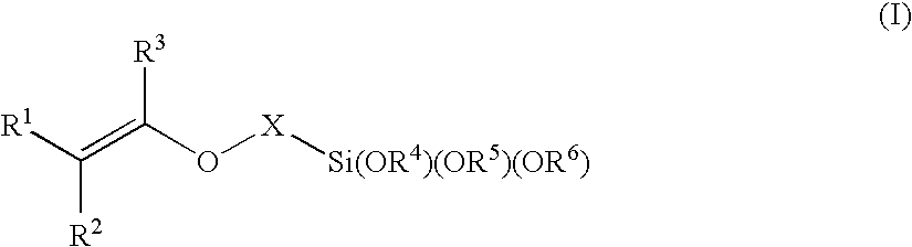
- wherein X is a linking group selected from the group consisting of —C(O)O—, —C(O)—, —OC(O)—, —O—C(O)—C(O)—O—, NHC(O)—O—, —O—C(O)—O—, a linear or a branched alkylene having 1 to 7 carbon atoms, a cycloalkylene having 3 to 17 carbon atoms, an alkylcycloalkylene having 4 to 20 carbon atoms and a cycloalkylalkylene having 4 to 20 carbon atoms;
- wherein each R1, R2, R3, R4, R5, and R6 (R1-R6) is independently selected from the group consisting of a hydrogen atom and a hydrocarbyl substituent with a primary, a secondary or a tertiary carbon attachment point, said hydrocarbyl group selected from the group consisting of an alkyl group, an alkenyl group, an alkynyl group, an aralkyl group, an alkaryl and an aryl group, each alkyl, alkenyl, alkynyl, aralkyl, alkaryl or aryl group having 1 to 20 carbon atom and each alkyl group of the aralkyl, or alkaryl groups may be linear, branched or cyclic; and
- any two R1-R6 in the same molecule may be linked to form at least one carbon ring containing 3 to 8 carbon atoms.
- In one example, the adhesion promoter is O-(vinyloxybutyl)-H-(triethoxysilylpropyl)-urethane (manufactured by Gelest, Inc., 11 East Steel Road, Morrisville, Pa. 19067).
- In
FIG. 1B , a puddle ofmolding composition 120 is dispensed on a top surface of adhesion layer 115 (or on a top surface oftransfer layer 110 ifadhesion layer 115 is not used). In one example, puddle ofmolding composition 120 is applied using drops of between about 1 micron and about 200 microns in diameter. - In one example, the material of puddle of
molding composition 120 comprises at least one aromatic divinyl ether, examples of which include 1,3-benzenedimethyl divinyl ether (structure II) and 1,3-benzenediethyl divinyl ether (structure III) -

- a photoacid generator (PAG), an optional stabilizer/sensitizer and an optional release agent.
- The molding composition advantageously includes a PAG. PAGs are compounds that generate an acid upon exposure to radiation and will cause cross-linking or enhance cross-linking of the molding layer. In one example between about 0.2 parts to about 10 parts of PAG is added to the molding composition per 100 parts of molding material. Examples of suitable PAGs include but are not limited to:
- sulfonium salts, examples of which include tolyldipenylsulfonium triflate, triphenylsulfonium perfluoromethanesulfonate (triphenylsulfonium triflate), triphenylsulfonium perfluorobutanesulfonate, triphenylsulfonium perfluoropentanesulfonate, triphenylsulfonium perfluorooctanesulfonate, triphenylsulfonium hexafluoroantimonate, triphenylsulfonium hexafluoroarsenate, triphenylsulfonium hexafluorophosphate, triphenylsulfonium bromide, triphenylsulfonium chloride, triphenylsulfonium iodide, 2,4,6-trimethylphenyldiphenylsulfonium perfluorobutanesulfonate, 2,4,6-trimethylphenyldiphenylsulfonium benzenesulfonate, tris(t-butylphenyl)sulfonium, diphenylethylsulfonium chloride, and phenacyldimethylsulfonium chloride;
- halonium salts, particularly iodonium salts, examples of which include diphenyliodonium perfluoromethanesulfonate (diphenyliodonium triflate), diphenyliodonium perfluorobutanesulfonate, diphenyliodonium perfluoropentanesulfonate, diphenyliodonium perfluorooctanesulfonate, diphenyliodonium hexafluoroantimonate, diphenyliodonium hexafluoroarsenate, bis-(t-butylphenyl)iodonium triflate, and bis-(t-butylphenyl)-iodonium camphorsulfonate;
- α,α′-bis-sulfonyl-diazomethanes, examples of which include bis(p-toluenesulfonyl)diazomethane, methylsulfonyl p-toluenesulfonyldiazomethane, 1-cyclohexylsulfonyl-1-(1,1dimethylethylsulfonyl) diazomethane, and bis(cyclohexylsulfonyl)diazomethane;
- trifluoromethanesulfonate esters of imides and hydroxyimides, examples of which include (trifluoromethylsulfonyloxy)-bicyclo[2.2.1]hept-5-ene-2,3-dicarboximide (MDT);
- nitrobenzyl sulfonate esters, examples of which include as 2-nitrobenzyl p-toluenesulfonate, 2,6-dinitrobenzyl p-toluenesulfonate, and 2,4-dinitrobenzyl p-trifluoromethylbenzenesulfonate;
- sulfonyloxynaphthalimides, examples of which include N-camphorsulfonyloxynaphthalimide and N-pentafluorobenzenelsulfonyloxynaphthalimide;
- pyrogallol derivatives (e.g., trimesylate of pyrogallol);
- naphthoquinone-4-diazides;
- alkyl disulfones;
- s-triazine derivatives; and
- miscellaneous sulfonic acid generators including t-butylphenyl-α-(p-toluenesulfonyloxy)-acetate, t-butyl-α-(p-toluenesulfonyloxy)acetate, and N-hydroxynaphthalimide dodecane sulfonate (DDSN), and benzoin tosylate.
- Examples of PAGs advantageously soluble in molding compositions based on aromatic divinyl ether, are represented by structures represented by structures (IV) and (V):
-

- wherein Tf=CF3S(O)2O—, and
-

- wherein R=CF2CF2CF2CF2H, CF3, or CF2CF3.
- Structure (IV) is sensitive to 313 nm UV radiation and is insensitive to i-line (365 nm UV radiation). However, addition of about 15% by weight (relative to the weight of any PAG in the molding composition) of one or more sensitizer/stabilizers, such as 9-anthracenemethanol (structure VI), or less than about 0.75% by weight (relative to the weight of aromatic divinyl ethers in the molding composition) of sensitizer/stabilizer added to the molding composition renders structure (IV) sensitive to 365 nm radiation.
-

- Structure (V) is sensitive to 365 nm radiation and does not require a sensitizer. However a sensitizer/stabilizer may be added as a stabilizing agent for improved shelf-life.
- Other suitable sensitizer/stabilizers may be used. In one example, the optional sensitizer/stabilizer may be a substituted 9-anthracenemethanol having the structure (VII), phenothiazine, or a substituted phenothiazine having the structure (VIII)
-

- wherein each R7, R8, R9, R10, R11, R12, R13, R14, R15 and R16 (R7-R16) is independently selected from the group consisting of a hydrogen atom and a hydrocarbyl substituent with a primary, a secondary or a tertiary carbon attachment point, said hydrocarbyl group selected from the group consisting of an alkyl group having 1 to 20 carbon atoms, an alkenyl group having 1 to 20 carbon atoms, an alkynyl group having 1 to 20 carbon atoms, an aralkyl group having 1 to 20 carbon atoms, an alkaryl having 1 to 20 carbon atoms and an aryl group having 1 to 20 carbon atoms;
- wherein the alkyl groups of the aralkyl and the alkaryl groups may be linear, branched or cyclic; and
- wherein any two R7-R15 in the same molecule may be linked to form the at least one carbon ring containing 3 to 8 carbon atoms. Phenothiazines should not be used with PAGs having structures V and VI or violent reactions may occur.
- In order to facilitate release of the exposed molding layer from the template (as described infra), materials with a low surface energy such as fluorinated vinyl ethers and other fluorinated compounds can be optionally included in the molding composition in amounts ranging from about 1% by weight of the molding composition to about 20% by weight of the molding composition. An example of a fluorinated vinyl ether is vinyl 2,2,2-trifluoroethyl ether. Another example of a fluorinated vinyl ether is structure (IX):
-

- Other fluorinated vinyl ethers having the formula
- (R17)(R18)═C(R19)OCn(R20)(R21)(D)(R22)(R23)(R24), wherein D is a carbon atom, wherein n is 1, wherein R17, R18, R19, R20 and R21 are H, and wherein R22, R23 and R24 are fluorine groups.
- In
FIG. 1C , atemplate 125 is aligned tosubstrate 100.Template 125 includes asupport portion 130 and amold portion 135. Bothsupport 130 portion andmold portion 135 are transparent to the wavelength of radiation thatmolding composition 120 is sensitive to (in one example 313 nm and/or 365 nm).Mold portion 135 includes a relief pattern made up of trenches (or grooves) 140 and plateaus (or lands) 145. Anoptional release layer 150 may be applied to the bottom and sidewalls oftrenches 140 and plateaus 145. Alternativelytemplate 125 may be monolithic andsupport portion 130 andmold portion 135 integral with each other. - In
FIG. 1D ,template 125 is pressed with a low pressure (i.e., less than about 1 psi) towardsubstrate 100, and the puddle of molding composition 120 (seeFIG. 1C ) is spread out over second adhesion layer 115 (ortransfer layer 110, if the second adhesion layer is not used), completely fillingtrenches 140 betweenplateaus 145 and forming anuncured molding layer 120A.Plateaus 145 do not touch second adhesion layer 115 (ortransfer layer 110, if the second adhesion layer is not used) somolding layer 120A is a continuous layer having thick and thin regions. After exposure to actinic radiation (in this case UV light) and removal oftemplate 125,uncured molding layer 120A is converted to a cured (i.e. cross-linked)molding layer 120B as depicted inFIG. 1E . - In
FIG. 1E , cured molding layer comprisesthin regions 155 andthick regions 160. Whentransfer layer 110 comprises a PVBA,second adhesion layer 115 comprises a material having a trialkoxysilyl moiety and a vinyl ether moiety (for example, structure I). The trialkoxysilyl moiety reacts with the carboxylic acid group of the transfer layer material and the vinyl group of the adhesion layer material polymerizes with the vinyl ether groups of the molding layer material to covalently link the transfer layer to the molding layer. - In a conventional SFIL process, a halocarbon-based anisotropic plasma etch would be performed at this point to remove
thin regions 155 and expose adhesion layer 115 (or transfer layer 110). However, this is not required for the embodiments of the present invention, so the thickness ofthin region 155 can be thicker than in conventional SFIL processes. - In
FIG. 1F , abackfill layer 175 is formed over curedmolding layer 120B, completely filling the space betweenthick regions 160 and covering boththin regions 155 andthick regions 160. - In a first example,
backfill layer 175 may comprise siloxane polymers, spin-on-glass (SOG) or organo silicate glass (OSG) materials including silsesquioxane resins (low molecular weight polymers or oligomers) which may be represented by the formulas —(SiO2)n-, —(R′SiO3/2)n-, —(R′2SiO)n- and —(R″Si2O3)n-, wherein R′ is selected from the group consisting of an alkyl group having 1 to 3 carbon atoms, an aryl group having 6 to 12 carbon atoms, and a cycloalkyl group having 6 to 12 carbon atoms, and wherein R″ is selected from the group consisting of an alkylene group having 1 to 2 carbon atoms and a cycloalkylene group having 6 to 12 carbon atoms. - In a second example,
backfill layer 175 may comprise any polymer containing at least 6 percent by weight of a metal such as silicon, germanium, tin, titanium or other Group IVA/IVB metals. - In a third example,
backfill layer 175 comprises one or more silicon containing vinyl ethers such as CH2═CHOCH2Si(CH3)3, CH2═CHOCH2CH2Si(CH3)3, CH2═CHOCH2Si(CH3)2CH2OCH═CH2, CH2═CHOCH2Si(CH3)2OSi(CH3)2CH2OCH═CH2, CH2═CHOCH2CH2Si(CH3)2CH2CH2OCH═CH2, CH(CH3)═CHOCH2Si(CH3)(CH2OCH═CH(CH3))CH2OCH═CH(CH3), CH2═CHOCH2CH2Si(Si(CH3)3)3 and a suitable photoacid generator. - In a fourth example,
backfill layer 175 comprises one or more silicon containing acrylates and a radical photoinitiator. - In
FIG. 1G , an optional exposure (for backfill compositions comprising silicon containing vinyl ethers and a PAG, such as example 3 supra) actinic radiation is performed (in this case UV light) and backfill layer 175 (seeFIG. 1F ) is converted to a cured (i.e., cross-linked)backfill layer 175A. - In
FIG. 1H , curedbackfill layer 175A (seeFIG. 1G ) or uncured backfill layer 175 (seeFIG. 1F ) is thinned and planarized to formetch barrier islands 175B of cured or uncured backfill material thereby exposing curedmolding layer 120B between the etch barrier islands. Atop surface 180 of curedmolding layer 120B is coplanar withtop surfaces 185 ofetch barrier islands 175B, ortop surface 180 may be recessed below tops surfaces 185. In one example, ifetch barrier islands 175B are formed from cured molding material, then the thinning and planarizing may be accomplished by either CMP or a plasma etch. In one example, ifetch barrier islands 175B are formed from uncured molding material, then the thinning and planarizing may be accomplished by a plasma etch. - In
FIG. 1I , an oxygen or reducing-chemistry anisotropic plasma etch process is performed to remove those portions of curedmolding layer 120B andsecond adhesion layer 115 not protected byetch barrier islands 175B, thereby exposing the top surface oftransfer layer 110. - In
FIG. 1J , the oxygen or reducing-chemistry anisotropic plasma etch process ofFIG. 1I is continued, to remove those portions oftransfer layer 110 andfirst adhesion layer 105 not protected byetch barrier islands 175B, thus exposing the top surface ofsubstrate 100. Curedetch barrier islands 175B may be thinned by the oxygen or reducing-chemistry anisotropic plasma etch process (as shown inFIG. 1J ), or alternatively the cured etch barrier islands may be removed by the oxygen or reducing-chemistry anisotropic plasma etch process. - In
FIG. 1K , a halocarbon-based anisotropic plasma etch is performed to etchtrenches 190 intosubstrate 100 whereversubstrate 100 is not protected bytransfer layer 110. Any remnants of curedetch barrier islands 175B (seeFIG. 1G ) not removed by the oxygen or reducing-chemistry anisotropic plasma etch process ofFIG. 1G are removed by the halocarbon-based anisotropic plasma etch. - In
FIG. 1L , the remainingtransfer layer 110 and first adhesion layer 105 (seeFIG. 1H ) are removed using organic solvents such as 2-ethoxyethanol, 2-methoxyethanol, 1-methoxy-2-propanol, N-methylpyrrolidone or an aqueous base whentransfer layer 110 is PVBA. Iftransfer layer 110 comprises a thermosetting polymer, a thermoplastic polymer, a polyepoxy polymer, a polyamide polymer, a polyimide polymer, a polyurethane polymer, a polycarbonate polymer or a polyester polymer, then plasma or acid removal processes are required. - Thus, the pattern of
plateaus 145 of template 125 (seeFIG. 1C ) has been converted to a pattern oftrenches 190 in substrate 100 (seeFIG. 1I ) in a negative imaging process in the first embodiment of the present invention without the use of a residual layer removal or pre-burning step. -
FIGS. 2A through 2K are cross-sectional drawings illustrating a SFIL process according to a second embodiment of the present invention. InFIGS. 2A through 2J ,adhesion layer 115 is optional and its composition has been described supra.FIG. 2A is similar toFIG. 1A ,FIG. 2B is similar toFIG. 1B , andFIG. 2C is similar toFIG. 1C , except there is no transfer layer or second adhesion layer and puddle ofmolding composition 120 is formed on the top surface ofadhesion layer 115 or the top surface ofsubstrate 100 if no adhesion layer is used. An advantage of using aromatic vinyl ethers in the molding composition is that a single layer of material can serve as both the molding layer and the transfer layer, eliminating the need to apply a separate aromatic transfer layer. -
FIGS. 2D , 2E, 2F, 2G and 2H are similar toFIGS. 1D , 1E, 1F, 1G and 1H respectively. In reference toFIG. 2E , the triethoxysilyl moiety of adhesion layer 115 (structure I) reacts with the —OH group on the surface ofsubstrate 100, and the vinyl ether moiety of structure (I) is co-polymerized into themolding layer 120B forming a covalent bond between the substrate and the cured layer. - In
FIG. 21 , an oxygen or reducing-chemistry anisotropic plasma etch process is performed to remove those portions of curedmolding layer 120B andadhesion layer 115 not protected byetch barrier islands 175B, thus exposing the top surface ofsubstrate 100. - In
FIG. 2J , a halocarbon RIE is performed to etchtrenches 190 intosubstrate 100 whereversubstrate 100 is not protectedetch barrier islands 175B (or protected by curedmolding layer 120B in the event all of the etch barrier island material is removed during the oxygen or reducing-chemistry anisotropic plasma etch process ofFIG. 21 or during the current halocarbon-based anisotropic plasma etch). Even thoughetch barrier islands 175B are thinned inFIG. 2J , any remnants ofetch barrier islands 175B not removed by the oxygen or reducing-chemistry anisotropic plasma etch process ofFIG. 21 are removed by the halocarbon-based anisotropic plasma etch ofFIG. 2J . - In
FIG. 2K , the curedmolding layer 120B (seeFIG. 2J ) is removed using a plasma or acid removal processes. - Thus, the pattern of
trenches 140 of template 125 (seeFIG. 2C ) has been converted to a pattern oftrenches 190 in substrate 100 (seeFIG. 2L ) in a negative imaging process in the second embodiment of the present invention without the use of a residual layer removal or a pre-burning step and without the use of a transfer layer. -

- To a two-liter, 3-necked round-bottomed flask equipped with a 500-ml constant pressure addition funnel, an overhead stirrer, a thermocouple and a nitrogen inlet was added 27 g (0.74 mol) of lithium aluminum hydride (95%) and 1000 ml of anhydrous tetrahydrofuran (THF). The addition funnel was charged with a solution of 100 g (0.493 mol) of isophthaloyl dichloride in 400 ml of anhydrous THF. Diacylchloride was added slowly over a period of 2 hours with cooling in an ice bath. Once addition was complete the ice bath was removed and the suspension allowed to reach room temperature for four hours at which time it was re-cooled and 200 ml of ethyl acetate was slowly added to decompose the remaining hydride. The addition funnel was recharged with 200 ml of 2M NaOH, which was then added slowly with vigorous stirring until the ensuing suspension became granular in appearance. The suspension was filtered and well washed with ethyl acetate. The combined filtrate and washings were then washed with brine, dried over anhydrous magnesium sulfate and evaporated on a rotary evaporator to yield 64 g (94%) of the title compound as a clear, colorless oil which solidified upon standing.
- To a two-liter round bottomed flask equipped with a positive-pressure nitrogen inlet and a magnetic stir bar was added 64 g (0.46 mol) of 1,3-benzenedimethanol, 10 g (0.03 mol) of mercuric acetate and 1 liter of ethyl vinyl ether. The solution was stirred at room temperature for four days at which time it was washed well with saturated sodium bicarbonate solution and brine. The solution was then stirred for three days over 20 g of anhydrous magnesium sulfate (the reaction is driven to completion by stirring over the acidic magnesium sulfate), filtered and evaporated on a rotary evaporator. The resulting oil was distilled twice through an 8″ Vigreux to yield 53 g (60%) of the title compound, boiling point=84° C. at 1 mm Hg. An additional 22 g of product was contaminated with the monovinyl ether intermediate.
-

- To a two-liter, 3-necked round-bottomed flask equipped with a 500-ml constant pressure addition funnel, an overhead stirrer, thermocouple and nitrogen inlet was added 16 g (0.42 mol) of lithium aluminum hydride (95%) and 800 ml of anhydrous THF. The addition funnel was charged with a solution of 40 g (0.21 mol) of 1,3-phenylenediacetic acid in 500 ml of anhydrous THF. The diacid was added slowly over a period of 2 hours with cooling in an ice bath. Once addition was complete, the ice bath was removed and the suspension allowed to reach room temperature overnight after which time it was re-cooled and 100 ml of ethyl acetate was slowly added to decompose the remaining hydride. The addition funnel was recharged with 200 ml of 2M NaOH, which was then added slowly with vigorous stirring until the ensuing suspension became granular in appearance. The suspension was filtered and well washed with ethyl acetate. The combined filtrate and washings were then washed with brine, dried over anhydrous magnesium sulfate and evaporated on a rotary evaporator to yield 21 g (62%) of the title compound as a clear, colorless oil.
- To a one-liter round bottomed flask equipped with a positive-pressure nitrogen inlet and a magnetic stir bar was added 21 g (0.13 mol) of 1,3-benzenediethanol, 4 g (0.03 mol) of mercuric acetate and 750 ml of ethyl vinyl ether. The solution was stirred at room temperature for four days at which time it was washed well with saturated sodium bicarbonate solution and brine. The solution was then stirred for three days over 20 g of anhydrous magnesium sulfate (the reaction is driven to completion by stirring over the acidic magnesium sulfate) filtered and evaporated on a rotary evaporator. The resulting oil was distilled twice through an 8″ Vigreux to yield 12 g (43%) of the title compound, boiling point=98° C. at 1 mm Hg. An additional 8 g of product was contaminated with the monovinyl ether intermediate.
- Structure (V) with R=CF2CF3 (0.03018 g) and 9-anthracenemethanol (0.0015 gram) were dissolved in 1.0015 g of 1,3-benzenedimethyl divinyl ether. A similar formulation was prepared by replacing 20 wt % of the 1,3-benzenedimethyl divinyl ether with 3,4,5,6-nonafluorohexyl vinyl ether. Both formulations were placed between two NaCl disks and were subjected to infrared (IR) analysis to determine the degree of curing as a function of ultraviolet (UV) light dose. 1,3-Benzenediethyl divinyl ether was found to cure as rapidly as 1,3-benzenedimethyl divinyl ether. Both aromatic divinyl ethers have only negligible volatility at room temperature, which is a desirable property as SFIL materials.
- A cured mixture of 1,3-benzenedimethyl divinyl ether and structure (V) with R=CF2CF3 was etched in an anisotropic fluorocarbon (CF4) plasma at 1.23 nm/sec, comparable to poly(4-vinylbenzoic acid) (1.3 nm/sec), while a cured aliphatic divinyl ether showed a faster etch rate of 1.65 nm/sec.
- Imprinting of the 1,3-benzenedimethyl divinyl ether formulations with and without fluorinated vinyl ether hand-dispensed on an Molecular Imprint tool was successful, generating 50 nm 1:1 line space patterns with an aspect ratio of about two as illustrated in
FIG. 3 . -
FIG. 3 is a scanning electron microscope image of an SFIL imprint image formed according to the embodiments of the present invention. The 1,3-benzenedimethyl divinyl ether formulations had a viscosity of about 1.6 cP and 50 nm wide line/space pairs were imprinted greater than 90 nm deep. - Thus, the embodiments of the present invention provide alternative SFIL-R formulations and SFIL-R process that are less sensitive to the presence oxygen, have relatively high curing rates, low volatility, low viscosity and high tensile strength.
- The description of the embodiments of the present invention is given above for the understanding of the present invention. It will be understood that the invention is not limited to the particular embodiments described herein, but is capable of various modifications, rearrangements and substitutions as will now become apparent to those skilled in the art without departing from the scope of the invention. Therefore, it is intended that the following claims cover all such modifications and changes as fall within the true spirit and scope of the invention.
Claims (24)


(R17)(R18)═C(R19)OCn(R20)(R21)(D)(R22)(R21)(R24),


(R17)(R18)═C(R19)OCn(R20)(R21)(D)(R22)(R23)(R24),


(R17)(R18)═C(R19)OCn(R20)(R21)(D)(R22)(R23)(R24),
Priority Applications (2)
| Application Number | Priority Date | Filing Date | Title |
|---|---|---|---|
| US12/055,513 US8262961B2 (en) | 2006-06-26 | 2008-03-26 | Aromatic vinyl ether based reverse-tone step and flash imprint lithography |
| US13/564,812 US8759415B2 (en) | 2006-06-26 | 2012-08-02 | Aromatic vinyl ether based reverse-tone step and flash imprint lithography |
Applications Claiming Priority (2)
| Application Number | Priority Date | Filing Date | Title |
|---|---|---|---|
| US11/426,363 US20070298176A1 (en) | 2006-06-26 | 2006-06-26 | Aromatic vinyl ether based reverse-tone step and flash imprint lithography |
| US12/055,513 US8262961B2 (en) | 2006-06-26 | 2008-03-26 | Aromatic vinyl ether based reverse-tone step and flash imprint lithography |
Related Parent Applications (1)
| Application Number | Title | Priority Date | Filing Date |
|---|---|---|---|
| US11/426,363 Continuation US20070298176A1 (en) | 2006-06-26 | 2006-06-26 | Aromatic vinyl ether based reverse-tone step and flash imprint lithography |
Related Child Applications (1)
| Application Number | Title | Priority Date | Filing Date |
|---|---|---|---|
| US13/564,812 Division US8759415B2 (en) | 2006-06-26 | 2012-08-02 | Aromatic vinyl ether based reverse-tone step and flash imprint lithography |
Publications (2)
| Publication Number | Publication Date |
|---|---|
| US20080174051A1 true US20080174051A1 (en) | 2008-07-24 |
| US8262961B2 US8262961B2 (en) | 2012-09-11 |
Family
ID=38873871
Family Applications (3)
| Application Number | Title | Priority Date | Filing Date |
|---|---|---|---|
| US11/426,363 Abandoned US20070298176A1 (en) | 2006-06-26 | 2006-06-26 | Aromatic vinyl ether based reverse-tone step and flash imprint lithography |
| US12/055,513 Active 2028-12-27 US8262961B2 (en) | 2006-06-26 | 2008-03-26 | Aromatic vinyl ether based reverse-tone step and flash imprint lithography |
| US13/564,812 Active 2026-07-19 US8759415B2 (en) | 2006-06-26 | 2012-08-02 | Aromatic vinyl ether based reverse-tone step and flash imprint lithography |
Family Applications Before (1)
| Application Number | Title | Priority Date | Filing Date |
|---|---|---|---|
| US11/426,363 Abandoned US20070298176A1 (en) | 2006-06-26 | 2006-06-26 | Aromatic vinyl ether based reverse-tone step and flash imprint lithography |
Family Applications After (1)
| Application Number | Title | Priority Date | Filing Date |
|---|---|---|---|
| US13/564,812 Active 2026-07-19 US8759415B2 (en) | 2006-06-26 | 2012-08-02 | Aromatic vinyl ether based reverse-tone step and flash imprint lithography |
Country Status (1)
| Country | Link |
|---|---|
| US (3) | US20070298176A1 (en) |
Cited By (5)
| Publication number | Priority date | Publication date | Assignee | Title |
|---|---|---|---|---|
| US20070029686A1 (en) * | 2004-04-28 | 2007-02-08 | Nikon Corporation | Pattern transfer method |
| US20100201043A1 (en) * | 2009-02-09 | 2010-08-12 | International Business Machines Corporation | Vinyl ether resist formulations for imprint lithography and processes of use |
| US20110042862A1 (en) * | 2009-08-21 | 2011-02-24 | International Business Corporation | Stabilizers for Vinyl Ether Resist Formulations for Imprint Lithography |
| US8759415B2 (en) | 2006-06-26 | 2014-06-24 | International Business Machines Corporation | Aromatic vinyl ether based reverse-tone step and flash imprint lithography |
| EP2970547A4 (en) * | 2013-03-11 | 2016-10-26 | Ndsu Res Foundation | Monomers and polymers derived from natural phenols |
Families Citing this family (16)
| Publication number | Priority date | Publication date | Assignee | Title |
|---|---|---|---|---|
| JP5435879B2 (en) | 2008-02-14 | 2014-03-05 | 株式会社ダイセル | Curable resin composition for nanoimprint |
| US9429837B2 (en) * | 2008-05-20 | 2016-08-30 | Asml Netherlands B.V. | Aqueous curable imprintable medium and patterned layer forming method |
| US8084185B2 (en) * | 2009-01-08 | 2011-12-27 | International Business Machines Corporation | Substrate planarization with imprint materials and processes |
| JP5671302B2 (en) * | 2009-11-10 | 2015-02-18 | 富士フイルム株式会社 | Curable composition for imprint, pattern forming method and pattern |
| US8846534B1 (en) * | 2011-10-07 | 2014-09-30 | Western Digital (Fremont), Llc | Process for CMP with large feature size variation |
| US9780335B2 (en) * | 2012-07-20 | 2017-10-03 | 3M Innovative Properties Company | Structured lamination transfer films and methods |
| CN102850490B (en) * | 2012-08-10 | 2014-05-21 | 福州大学 | Method for preparing molecularly imprinted material by POSS compound as cross-linking agent |
| KR101408181B1 (en) * | 2012-11-21 | 2014-06-16 | 한국기계연구원 | Method for manufacturing substrate formed a nano pattern |
| US9711744B2 (en) | 2012-12-21 | 2017-07-18 | 3M Innovative Properties Company | Patterned structured transfer tape |
| US20140175707A1 (en) | 2012-12-21 | 2014-06-26 | 3M Innovative Properties Company | Methods of using nanostructured transfer tape and articles made therefrom |
| KR102243630B1 (en) * | 2013-12-30 | 2021-04-23 | 캐논 나노테크놀로지즈 인코퍼레이티드 | Methods for uniform imprint pattern transfer of sub-20 nm features |
| TWI651593B (en) * | 2014-03-14 | 2019-02-21 | 日商Jsr股份有限公司 | Manufacturing method of wiring, radiation sensitive composition, electronic circuit, and electronic device |
| KR102201321B1 (en) | 2014-07-25 | 2021-01-11 | 삼성전자주식회사 | Method of fabricating aligned pattern on pattern formation area using imprint process |
| WO2018026378A1 (en) * | 2016-08-05 | 2018-02-08 | Applied Materials, Inc. | Method of imprint lithography of conductive materials; stamp for imprint lithography, and apparatus for imprint lithograph |
| US11501969B2 (en) | 2019-01-22 | 2022-11-15 | International Business Machines Corporation | Direct extreme ultraviolet lithography on hard mask with reverse tone |
| CN110746559B (en) * | 2019-11-07 | 2022-02-25 | 东北林业大学 | Preparation method of porous carbon-based triazine molecularly imprinted polymer and method for extracting triazine pesticide in agricultural products by using porous carbon-based triazine molecularly imprinted polymer |
Citations (10)
| Publication number | Priority date | Publication date | Assignee | Title |
|---|---|---|---|---|
| US6033828A (en) * | 1997-01-27 | 2000-03-07 | Shin-Etsu Chemical Co., Ltd. | Partially hydrogenated polymers and chemically amplified positive resist compositions |
| US6110653A (en) * | 1999-07-26 | 2000-08-29 | International Business Machines Corporation | Acid sensitive ARC and method of use |
| US6312869B1 (en) * | 1996-04-24 | 2001-11-06 | Shin-Etsu Chemical, Co., Ltd. | Chemically amplified positive resist composition, pattern forming method, and method for preparing polymer having a crosslinking group |
| US6334960B1 (en) * | 1999-03-11 | 2002-01-01 | Board Of Regents, The University Of Texas System | Step and flash imprint lithography |
| US20050160934A1 (en) * | 2004-01-23 | 2005-07-28 | Molecular Imprints, Inc. | Materials and methods for imprint lithography |
| US20050214674A1 (en) * | 2004-03-25 | 2005-09-29 | Yu Sui | Positive-working photoimageable bottom antireflective coating |
| US20050255410A1 (en) * | 2004-04-29 | 2005-11-17 | Guerrero Douglas J | Anti-reflective coatings using vinyl ether crosslinkers |
| US20060111454A1 (en) * | 2004-11-24 | 2006-05-25 | Molecular Imprints, Inc. | Composition to reduce adhesion between a conformable region and a mold |
| US20070051697A1 (en) * | 2005-09-02 | 2007-03-08 | Dipietro Richard A | Processes and materials for step and flash imprint lithography |
| US7416831B2 (en) * | 2004-08-20 | 2008-08-26 | Eastman Kodak Company | Substrate for lithographic printing plate precursor |
Family Cites Families (5)
| Publication number | Priority date | Publication date | Assignee | Title |
|---|---|---|---|---|
| US3910187A (en) * | 1971-08-30 | 1975-10-07 | Du Pont | Dry planographic printing plate |
| US5705116A (en) * | 1994-06-27 | 1998-01-06 | Sitzmann; Eugene Valentine | Increasing the useful range of cationic photoinitiators in stereolithography |
| JP2003295380A (en) * | 2002-03-29 | 2003-10-15 | Fuji Photo Film Co Ltd | Heat-developable image recording material |
| JP2005113012A (en) * | 2003-10-08 | 2005-04-28 | Konica Minolta Medical & Graphic Inc | Active ray-curable ink composition, image-forming method using the same and inkjet recording device |
| US20070298176A1 (en) | 2006-06-26 | 2007-12-27 | Dipietro Richard Anthony | Aromatic vinyl ether based reverse-tone step and flash imprint lithography |
-
2006
- 2006-06-26 US US11/426,363 patent/US20070298176A1/en not_active Abandoned
-
2008
- 2008-03-26 US US12/055,513 patent/US8262961B2/en active Active
-
2012
- 2012-08-02 US US13/564,812 patent/US8759415B2/en active Active
Patent Citations (12)
| Publication number | Priority date | Publication date | Assignee | Title |
|---|---|---|---|---|
| US6312869B1 (en) * | 1996-04-24 | 2001-11-06 | Shin-Etsu Chemical, Co., Ltd. | Chemically amplified positive resist composition, pattern forming method, and method for preparing polymer having a crosslinking group |
| US6033828A (en) * | 1997-01-27 | 2000-03-07 | Shin-Etsu Chemical Co., Ltd. | Partially hydrogenated polymers and chemically amplified positive resist compositions |
| US6334960B1 (en) * | 1999-03-11 | 2002-01-01 | Board Of Regents, The University Of Texas System | Step and flash imprint lithography |
| US6719915B2 (en) * | 1999-03-11 | 2004-04-13 | Board Of Regents, The University Of Texas System | Step and flash imprint lithography |
| US6110653A (en) * | 1999-07-26 | 2000-08-29 | International Business Machines Corporation | Acid sensitive ARC and method of use |
| US6319651B1 (en) * | 1999-07-26 | 2001-11-20 | International Business Machines Corporation | Acid sensitive ARC and method of use |
| US20050160934A1 (en) * | 2004-01-23 | 2005-07-28 | Molecular Imprints, Inc. | Materials and methods for imprint lithography |
| US20050214674A1 (en) * | 2004-03-25 | 2005-09-29 | Yu Sui | Positive-working photoimageable bottom antireflective coating |
| US20050255410A1 (en) * | 2004-04-29 | 2005-11-17 | Guerrero Douglas J | Anti-reflective coatings using vinyl ether crosslinkers |
| US7416831B2 (en) * | 2004-08-20 | 2008-08-26 | Eastman Kodak Company | Substrate for lithographic printing plate precursor |
| US20060111454A1 (en) * | 2004-11-24 | 2006-05-25 | Molecular Imprints, Inc. | Composition to reduce adhesion between a conformable region and a mold |
| US20070051697A1 (en) * | 2005-09-02 | 2007-03-08 | Dipietro Richard A | Processes and materials for step and flash imprint lithography |
Cited By (10)
| Publication number | Priority date | Publication date | Assignee | Title |
|---|---|---|---|---|
| US20070029686A1 (en) * | 2004-04-28 | 2007-02-08 | Nikon Corporation | Pattern transfer method |
| US7670747B2 (en) * | 2004-04-28 | 2010-03-02 | Nikon Corporation | Pattern transfer method |
| US8759415B2 (en) | 2006-06-26 | 2014-06-24 | International Business Machines Corporation | Aromatic vinyl ether based reverse-tone step and flash imprint lithography |
| US20100201043A1 (en) * | 2009-02-09 | 2010-08-12 | International Business Machines Corporation | Vinyl ether resist formulations for imprint lithography and processes of use |
| US8168691B2 (en) | 2009-02-09 | 2012-05-01 | International Business Machines Corporation | Vinyl ether resist formulations for imprint lithography and processes of use |
| US20110042862A1 (en) * | 2009-08-21 | 2011-02-24 | International Business Corporation | Stabilizers for Vinyl Ether Resist Formulations for Imprint Lithography |
| US8168109B2 (en) | 2009-08-21 | 2012-05-01 | International Business Machines Corporation | Stabilizers for vinyl ether resist formulations for imprint lithography |
| EP2970547A4 (en) * | 2013-03-11 | 2016-10-26 | Ndsu Res Foundation | Monomers and polymers derived from natural phenols |
| US9546122B2 (en) | 2013-03-11 | 2017-01-17 | Ndsu Research Foundation | Monomers and polymers derived from natural phenols |
| US9630897B2 (en) | 2013-03-11 | 2017-04-25 | Ndsu Research Foundation | Monomers and polymers derived from natural phenols |
Also Published As
| Publication number | Publication date |
|---|---|
| US8262961B2 (en) | 2012-09-11 |
| US20120291668A1 (en) | 2012-11-22 |
| US20070298176A1 (en) | 2007-12-27 |
| US8759415B2 (en) | 2014-06-24 |
Similar Documents
| Publication | Publication Date | Title |
|---|---|---|
| US8262961B2 (en) | Aromatic vinyl ether based reverse-tone step and flash imprint lithography | |
| US8128832B2 (en) | Processes and materials for step and flash imprint lithography | |
| US7435074B2 (en) | Method for fabricating dual damascence structures using photo-imprint lithography, methods for fabricating imprint lithography molds for dual damascene structures, materials for imprintable dielectrics and equipment for photo-imprint lithography used in dual damascence patterning | |
| US7648767B2 (en) | Material composition for nano- and micro-lithography | |
| US9159558B2 (en) | Methods of reducing defects in directed self-assembled structures | |
| US8293354B2 (en) | UV curable silsesquioxane resins for nanoprint lithography | |
| US8992790B2 (en) | Patterning process | |
| JP4028131B2 (en) | Photoresist polymer and method for producing the same, photoresist composition, and method for forming photoresist pattern | |
| US20170371240A1 (en) | Imprint resist with fluorinated photoinitiator and substrate pretreatment for reducing fill time in nanoimprint lithography | |
| US20050042538A1 (en) | Antireflective hardmask and uses thereof | |
| JP6797902B2 (en) | Substrate pretreatment and etching uniformity in nanoimprint lithography | |
| KR101680407B1 (en) | Pattern forming method | |
| US20070281242A1 (en) | Silsesquioxane Resin | |
| TW201327061A (en) | Silicon-containing resist underlayer film-forming composition and patterning process | |
| JP5074488B2 (en) | Silsesquioxane resin system containing a basic additive with electron withdrawing functionality | |
| US7749422B2 (en) | Release layer for imprinted photocationic curable resins | |
| US7141692B2 (en) | Molecular photoresists containing nonpolymeric silsesquioxanes | |
| US8017303B2 (en) | Ultra low post exposure bake photoresist materials | |
| US20110111345A1 (en) | Silicon containing coating compositions and methods of use | |
| US8926888B2 (en) | Fluorinated silazane release agents in nanoimprint lithography | |
| US20070269736A1 (en) | NEW SUB 40 NM RESOLUTION Si CONTAINING RESIST SYSTEM | |
| Kim | Development and study of nano-imprint and electron beam lithography materials for semiconductor devices |
Legal Events
| Date | Code | Title | Description |
|---|---|---|---|
| STCF | Information on status: patent grant |
Free format text: PATENTED CASE |
|
| AS | Assignment |
Owner name: GLOBALFOUNDRIES U.S. 2 LLC, NEW YORK Free format text: ASSIGNMENT OF ASSIGNORS INTEREST;ASSIGNOR:INTERNATIONAL BUSINESS MACHINES CORPORATION;REEL/FRAME:036550/0001 Effective date: 20150629 |
|
| AS | Assignment |
Owner name: GLOBALFOUNDRIES INC., CAYMAN ISLANDS Free format text: ASSIGNMENT OF ASSIGNORS INTEREST;ASSIGNORS:GLOBALFOUNDRIES U.S. 2 LLC;GLOBALFOUNDRIES U.S. INC.;REEL/FRAME:036779/0001 Effective date: 20150910 |
|
| FPAY | Fee payment |
Year of fee payment: 4 |
|
| AS | Assignment |
Owner name: WILMINGTON TRUST, NATIONAL ASSOCIATION, DELAWARE Free format text: SECURITY AGREEMENT;ASSIGNOR:GLOBALFOUNDRIES INC.;REEL/FRAME:049490/0001 Effective date: 20181127 |
|
| FEPP | Fee payment procedure |
Free format text: 7.5 YR SURCHARGE - LATE PMT W/IN 6 MO, LARGE ENTITY (ORIGINAL EVENT CODE: M1555); ENTITY STATUS OF PATENT OWNER: LARGE ENTITY |
|
| MAFP | Maintenance fee payment |
Free format text: PAYMENT OF MAINTENANCE FEE, 8TH YEAR, LARGE ENTITY (ORIGINAL EVENT CODE: M1552); ENTITY STATUS OF PATENT OWNER: LARGE ENTITY Year of fee payment: 8 |
|
| AS | Assignment |
Owner name: GLOBALFOUNDRIES INC., CAYMAN ISLANDS Free format text: RELEASE BY SECURED PARTY;ASSIGNOR:WILMINGTON TRUST, NATIONAL ASSOCIATION;REEL/FRAME:054479/0842 Effective date: 20200410 Owner name: TAIWAN SEMICONDUCTOR MANUFACTURING CO., LTD., TAIWAN Free format text: ASSIGNMENT OF ASSIGNORS INTEREST;ASSIGNOR:GLOBALFOUNDRIES INC.;REEL/FRAME:054482/0862 Effective date: 20200515 |
|
| AS | Assignment |
Owner name: GLOBALFOUNDRIES INC., CAYMAN ISLANDS Free format text: RELEASE BY SECURED PARTY;ASSIGNOR:WILMINGTON TRUST, NATIONAL ASSOCIATION;REEL/FRAME:054636/0001 Effective date: 20201117 |
|
| MAFP | Maintenance fee payment |
Free format text: PAYMENT OF MAINTENANCE FEE, 12TH YEAR, LARGE ENTITY (ORIGINAL EVENT CODE: M1553); ENTITY STATUS OF PATENT OWNER: LARGE ENTITY Year of fee payment: 12 |