US20080098277A1 - High density high reliability memory module with power gating and a fault tolerant address and command bus - Google Patents
High density high reliability memory module with power gating and a fault tolerant address and command bus Download PDFInfo
- Publication number
- US20080098277A1 US20080098277A1 US11/551,866 US55186606A US2008098277A1 US 20080098277 A1 US20080098277 A1 US 20080098277A1 US 55186606 A US55186606 A US 55186606A US 2008098277 A1 US2008098277 A1 US 2008098277A1
- Authority
- US
- United States
- Prior art keywords
- memory
- buffer device
- error
- memory module
- buffer
- Prior art date
- Legal status (The legal status is an assumption and is not a legal conclusion. Google has not performed a legal analysis and makes no representation as to the accuracy of the status listed.)
- Granted
Links
Images


Classifications
-
- H—ELECTRICITY
- H03—ELECTRONIC CIRCUITRY
- H03M—CODING; DECODING; CODE CONVERSION IN GENERAL
- H03M13/00—Coding, decoding or code conversion, for error detection or error correction; Coding theory basic assumptions; Coding bounds; Error probability evaluation methods; Channel models; Simulation or testing of codes
- H03M13/03—Error detection or forward error correction by redundancy in data representation, i.e. code words containing more digits than the source words
- H03M13/05—Error detection or forward error correction by redundancy in data representation, i.e. code words containing more digits than the source words using block codes, i.e. a predetermined number of check bits joined to a predetermined number of information bits
- H03M13/13—Linear codes
- H03M13/19—Single error correction without using particular properties of the cyclic codes, e.g. Hamming codes, extended or generalised Hamming codes
-
- G—PHYSICS
- G06—COMPUTING; CALCULATING OR COUNTING
- G06F—ELECTRIC DIGITAL DATA PROCESSING
- G06F11/00—Error detection; Error correction; Monitoring
- G06F11/07—Responding to the occurrence of a fault, e.g. fault tolerance
- G06F11/08—Error detection or correction by redundancy in data representation, e.g. by using checking codes
- G06F11/10—Adding special bits or symbols to the coded information, e.g. parity check, casting out 9's or 11's
- G06F11/1008—Adding special bits or symbols to the coded information, e.g. parity check, casting out 9's or 11's in individual solid state devices
- G06F11/1044—Adding special bits or symbols to the coded information, e.g. parity check, casting out 9's or 11's in individual solid state devices with specific ECC/EDC distribution
Definitions
- This invention relates generally to a high-density, high-reliability memory module with a fault tolerant address and command bus for use as a main memory that will achieve the degree of fault-tolerance and self-healing necessary for autonomic computing systems.
- Memory modules are well known to the prior art and have been and are presently being used in practical applications such as in computers and other equipment using solid state memories.
- main memories offer bandwidths in the range of 1.6 to 2.6 GB/s, and although some memories provide for limited data path error correction most offer no means of any error correction targeting the interface between the memory controller and the memory subsystem.
- memory modules for server products and other higher-end computing systems usually include re-drive logic for address and command inputs, and clock re-synchronization and re-drive circuitry associated with the memory subsystems to permit these modules to contain higher memory device counts and to ensure accurate clock timings at each device on the memory assembly.
- the present invention provides such a comprehensive system solution that includes the capability of high memory density and a high degree of fault tolerance and the overall differentiated system reliability long desired in the server market.
- the present invention is directed to a high density high reliability memory controller/interface module, provided with a high degree of compatibility with industry-standard solutions, capable of meeting the desired density, performance and reliability requirements and interfacing with the presently available memory modules, as well as with existing or enhanced support devices.
- the present invention accomplishes all these ends, resulting in a high density and enhanced reliability memory solution at low cost.
- An object of the present invention is to provide an enhanced 28 bit 1:2 register (also referred to herein as a “buffer”) that supports 4 ranks of memory devices, intended for use with memory subsystems such as Dual Inline Memory Modules (DIMMs) having Dynamic Random Access Memory (DRAM) chips thereon.
- the register of the present invention has added thereto additional command inputs, error correction code (ECC) logic to identify and correct single bit errors on the command or address bus, and permit continuous memory operation independent of the existence of these errors.
- ECC error correction code
- Another object of the present invention is to include in such DIMMs error latches and an error reporting mode whereby the system may interrogate the device to determine the error condition thereby allowing accurate fault determination and preventive maintenance—thereby reducing unplanned system outages.
- a further object of the present invention is to include redundant contacts on all connectors/DIMM interconnects that would otherwise be considered single points of failure whereby an intermittent or permanent contact failure would result in an unplanned system outage.
- Still another object of the present invention is to provide the DIMM with key operational features such as chip select gating of key inputs and programmable delay for un-gated inputs, thereby reducing module power and offering increased operational flexibility.
- a further object of the present invention is to provide a DIMM that can be readily utilized in presently available controllers in a manner most applicable to the market needs.
- Another further object of the present invention is to have a DIMM that uses connectors similar to those presently in use so that prior art contacts, molds, handlers and related production tools can continue to be used such that the modules can be more cheaply produced with additional density while providing value-added reliability, and other value-add attributes, such as a higher memory packaging density with minimal additional production costs.
- Another further object of the present invention is to have a buffer which is operable with up to 4 ranks of memory devices, that is also interchangeable with previously developed buffers limited to no more than 2 ranks of memory devices, and can be used as a direct replacement for said previously developed buffers on DIMMs that utilized said buffers—thereby eliminating the need to produce or procure two types of buffer devices or to re-design existing memory modules.
- the DIMM of the present invention is comprised of a printed circuit board having a front side and a back side and a plurality of double data rate (DDR) DRAMs or synchronous dynamic random access memories (SDRAMs) affixed to both the front surface and the back surface.
- DDR double data rate
- SDRAMs synchronous dynamic random access memories
- the contact means provided on the front and the back sides of the printed circuit card provide for electrically connecting the external circuitry to the SDRAMs in a direct or indirect manner.
- the server of the present invention comprises a novel DIMM provided with a new and unique ECC/ Parity Register that is operable with 1 to 4 memory ranks, coupled to a memory interface chip which is in turn coupled to a memory controller or processor such that the memory controller sends address and command information to the buffer (or register) via address/command lines together with check bits for error correction purposes to the ECC/ Parity register.
- Still another object of the invention is to provide for Parity error reporting in which the parity signal is delivered one cycle after the address and command to which it applies, and the error line be driven low two clocks after the address and command bits are driven to the DRAMs from the register on the DIMM. After holding the error line low for only 2 clock cycles, the driver can be disabled and the output permitted to return to an un-driven state (high impedance) thus allowing this line to be shared by multiple modules.
- the invention provides means for and a method for adjusting the propagation delay, for signals on the memory module that are not included in the ECC circuitry, such that the signals can be selectively re-driven by the buffer within one or two clock cycles.
- the present invention permits operation of the memory module in parity mode, such that unused ECC check bit inputs are held at a low level thus ensuring that these inputs are at a known and quiescent state.
- the present invention provides for reducing the probability of Single Point of Failures occurring by providing selected signals with redundant contacts directly on the opposite side of the DIMM from the original finction contact thereby reducing the probability of a contact failure resulting in an unplanned system outage.
- FIG. 1 is a block diagram of a typical server memory arrangement
- FIG. 2 is a block diagram of the enhanced server memory arrangement of the present invention.
- FIGS. 3A and 3B are plan views respectively of the front and back of the two hundred and seventy six (276) pin dual inline memory module (DIMM) of the present invention that utilizes up to 72 planar DRAMS; and FIGS. 3C and 3D are plan views respectively of the front and back of the 276 pin DIMM of the present invention that utilizes up to eighteen four high DRAM stacks;
- DIMM dual inline memory module
- FIGS. 4A and 4B are schematic views of the ECC/ Parity register, shown in FIG. 3A ;
- FIG. 5 is a block diagram of the single error correction/ double error detection error correction code (SEC/DED ECC) circuit of FIG. 4B ;
- FIG. 6 describes, in H—matrix form, the preferred ECC code selected for the module of FIG. 3 ;
- FIGS. 7A , 7 B and 7 C show the designated contacts or pin connections for the DIMM of FIGS. 3A and 3B ;
- FIG. 8 shows the timing diagram used with the present invention
- FIG. 10 shows the CS wiring between the buffers and the memory devices on the right and left side of the card, for a 4 rank DIMM of the present invention.
- FIG. 11 shows the IIC addresses that are utilized to access the error registers on the one or two buffers of the present invention.
- FIG. 1 is a block diagram of a typical server memory arrangement
- FIG. 2 is a block diagram of the enhanced server memory arrangement of the present invention
- FIGS. 3A and 3B are plan views respectively of the front and back of a 4 rank planar 276 contact dual inline memory module (DIMM) of the present invention
- FIGS. 3C and 3D are plan views respectively of the front and back of a 4 rank four high stacked 276 contact DIMM of the present invention
- FIGS. 4A and 4B are schematic views of the 4 rank-optimized buffer/register, parity and error correction circuits shown in FIGS. 3A and 3B (and FIGS.
- FIG. 5 is a block diagram of the single error correction/double error detection error correction code (SEC/DED ECC) circuit of FIG. 4B ;
- FIG. 6 describes, in H—matrix, form the preferred ECC code selected for the module of FIGS. 3A and 3C ;
- FIGS. 7A , 7 B and 7 C show the designated pin connections for the DIMM of FIGS. 3A and 3B (and FIGS. 3C and 3D ).
- FIG. 8 shows the timing diagram used with the present invention.
- FIG. 9 shows the buffer connections and total number of buffers used in a system when the buffer of the present invention is used on 1, 2 and 4 rank DIMMs;
- FIG. 9 shows the buffer connections and total number of buffers used in a system when the buffer of the present invention is used on 1, 2 and 4 rank DIMMs;
- FIG. 9 shows the buffer connections and total number of buffers used in a system when the buffer of the present invention is used on 1, 2 and 4 rank DIMMs;
- FIG. 10 shows the CS wiring between the buffers and the memory devices on the right and left side of the card, for a 4 rank DIMM of the present invention
- FIG. 11 is a table showing the IIC addresses that would be used to access the error registers on the one or two buffers of the present invention.
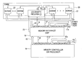
- Each DRAM 11 on the DIMM 10 has a plurality of input/output pins that are coupled, via the printed circuitry on the DIMM 10 to the contacts on the DIMM 10 and theses contacts are further coupled, via a data line 15 , to a memory interface chip 18 and to a memory controller or processor 19 .
- Each DRAM on the DIMM is further, coupled via such DIMM contacts, to a buffer/register 12 and to a phase locked loop circuit 14 on the DIMM.
- the phase locked loop 14 (PLL) is connected via clock line 17 to the memory interface chip 18 .
- the register 12 is also coupled to the memory interface chip 18 via an address and command (CMD) bus 16 .
- CMD address and command
- the memory interface chip 18 is coupled to the memory controller 19 via the data line 15 , address and command line 16 and clock line 17 . It should be understood that although only one such DIMM is shown in this figure that in actuality the server would contain many such DIMMs. Such other DIMMs would be coupled in a like manner to the memory interface chip 18 and memory controller 19 via data, address and command lines, and may be connected in a multi-drop, cascade interconnect or other connection method, depending on the system structure and buffer functionality. Since such servers and their operation are well known to those skilled in the art, further description of such servers and their operation is not deemed necessary.
- FIGS. 2 , 3 A, 3 B, 3 C, 3 D, 4 A, 4 B, 5 , 8 , 9 , 10 and 11 the enhanced server memory arrangement of the present invention will be described.
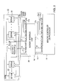
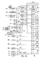
- FIG. 2 there is illustrated, in schematic form, a block diagram of a server memory arrangement employing the present invention.
- the server comprises a novel DIMM 20 provided with a novel ECC/Parity Buffer chip 21 (also referred to as a “buffer device”) coupled to the memory interface chip 18 which is in turn coupled to the memory controller or processor 19 .
- the chip 21 need not include both the ECC function and the parity finction.
- the chip 21 could have just the 4 rank addressability alone, the ECC finction alone or just the parity finction alone and still operate in accordance with the present invention. More specifically, as shown in this FIG.
- the memory interface chip 18 sends and receives data from the DIMMs via the data line 15 and sends address and commands via line 16 .
- the memory interface chip 18 then sends and receives data, via line 15 , to the memory devices, or DRAMs 22 and sends address and command information to the register chip 21 via add/cmd line 16 and check bits for error correction purposes to the ECC/ Parity register chip 21 via line 25 .
- the check bits and/or parity bits associated with the ECC/Parity register chip 21 are developed in the memory interface chip 18 , although in other embodiments these bits could be developed in the memory controller or processor 19 , be communicated to the memory interface chip as a subset of the information on line 16 and the memory interface would then re-drive this information to the memory module on line 25 .
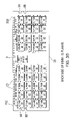
- the improvements in the DIMM 20 of the present invention are realized especially by enlarging the length of DIMM 20 to between 149 mm and 153 mm. Nominally the DIMM 20 is 151.35 mm (5.97 inches) long and its width is 54.6 mm (2.16 inches).
- the width of the DIMM 20 is sufficient in width to accommodate the four rows of DRAMs 22 installed thereon, in addition to the two buffers 21 (one buffer is mounted on each side in the exemplary embodiment, as shown in FIGS. 3A and 3B ), the PLL 24 and passive devices (not shown) such as resistors and capacitors, but must also be no wider than permitted by the available system physical dimensions for the module(s).
- the length of the DIMM 20 however must be such that the DIMM 20 can accommodate additional signal contacts, up to 138 , as well as up to thirty-six planar DRAMs 26 having a nominal body size of up to 11.5 mm wide by 11 mm tall and have a locating key or notch 9 a distance of between 82.675 mm from one end of the DIMM 20 and 68.675 mm from the other end of the DIMM as shown. Again it should be understood that these dimensions are nominal and may vary plus or minus 3 mm in various implementations.
- the DIMM 20 can also be provided with additional notches 9 a and 9 b on each side, i.e., the shorter edges of the DIMM 20 .
- each DIMM 20 in addition to the DRAMs, there is positioned a phase locked loop (PLL) chip 24 and the novel ECC/Parity Buffer chip 21 of the present invention.
- PLL phase locked loop
- This novel ECC/Parity Buffer chip 21 will be further described below and in detail in conjunction with FIGS. 4A and 4B It should be understood that the PLL chip 24 can be eliminated if its circuitry is provided on the buffer chip 21 or within the same package as the buffer chip 21 (i.e.
- the DIMM 20 depicted in FIGS. 3A and 3B also includes an EPROM 302 which is used for the storage of memory module attribute information (commonly referred to as an SPD data, when associated with memory modules), with the EPROM's IIC interface also shared, in this module, with the novel ECC/Parity Buffer chip, enabling one means for accessing status registers on the buffer chip(s).
- EPROM 302 which is used for the storage of memory module attribute information (commonly referred to as an SPD data, when associated with memory modules), with the EPROM's IIC interface also shared, in this module, with the novel ECC/Parity Buffer chip, enabling one means for accessing status registers on the buffer chip(s).
- Alternate configurations of the 4 rank DIMM 20 may be implemented by exemplary embodiments. See, for examples FIGS. 3C and 3D which depict front and back plan views of a 4 rank four high stacked 276 contact DIMM 20 of the present invention.
- the DIMM 20 also includes an EPROM device 302 which has the same function as device 302 in FIG. 3 A, which includes enabling one means for accessing status registers on the buffer chip(s).
- EPROM device 302 which has the same function as device 302 in FIG. 3 A, which includes enabling one means for accessing status registers on the buffer chip(s).
- other configurations for providing up to 4 ranks of memory may also be implemented without departing from the scope of the invention.
- a 4 rank two high, stacked 276 contact DIMM 20 may be implemented by exemplary embodiments.
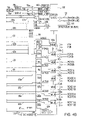
- This new, improved, larger sized DIMM 20 shown in these FIGS. 3A , 3 B, 3 C and 3 D also achieves a further significant improvement in the interconnect failure rate for the larger size of the module permits the connector system to accommodate two hundred and seventy-six contacts or pins 23 .
- These pins are numbered and coupled to respective inputs as shown in FIGS. 7 a , 7 b , and 7 c.
- Contact or pin number one (1) is identified and shown in FIG. 3A as contact 23 A and is on the left hand side of the front side of the DIMM 20 and is positioned approximately 5 . 175 mm from the left edge of the DIMM 20 and 77.5 mm from the center of the notch 9 .
- Contact or pin number one hundred and thirty-eight is identified and shown in FIG. 3A as contact 23 B and is on the right hand side of the front side of the DIMM 20 and is positioned approximately 5.175 mm from the right edge of the DIMM 20 and approximately 63.5 mm from the center of the notch 9 .
- Contact or pin number one hundred and thirty-nine is identified and shown in FIG. 3B as contact 23 C and is directly opposite contact number one 23 A and is also positioned approximately 5.175 mm from the right edge of the back of DIMM 20 and is also 77.5 mm from the center of the notch 9 .
- Contact or pin number two hundred and seventy-six is identified in shown in FIG.
- contact 23 D is directly opposite contact number one hundred and thirty-eight 23 B and is also positioned approximately 5.175 mm from the left edge of the back of DIMM 20 and 63.5 mm from the center of the notch 9 .
- the greater size of this DIMM 20 also accommodates the inclusion of a new and larger ECC/Parity buffer chip 21 required by the present invention. Because the two hundred and seventy-six contacts or pins 23 on this larger DIMM 20 are more than sufficient to meet the needs of all the circuitry on the DIMM 20 this means that the DIMM 20 provides extra or redundant contacts. These extra or redundant contacts or pins 23 can now be used to provide additional protection for certain selected signal or voltage lines, for which error correction is not possible.
- the present invention by providing such redundant contacts, effectively eliminates concerns such as contact failures on clock inputs, CS, CKE, and ODT inputs, Vref inputs, and other signals not protected by ECC.
- Other benefits include the elimination or reduction of concerns regarding power supply noise and/or voltage drops due to scarcity of voltage (VDD) contacts in the data region as well providing additional ground pins in the address/ control region on the DIMM 20 .
- the larger contact count of the present invention also permits the DIMM 20 to be wired such that they are consistent with prior art DIMMs.
- the additional contacts 23 also permit the inclusion of ECC check bits, associated with address and command inputs, allowing for real-time system monitoring of faults associated with these inputs, as well as system interrogation of fault counts and attributes. These faults would result in catastrophic system outages in conventional prior art systems using the smaller prior art DIMMs.
- the server would contain many such DIMMs.
- the DIMM 20 of the present invention, is provided with a plurality of SDRAMs 22 , a phase locked loop circuit 24 and the ECC/Parity buffer chips 21 .
- the ECC/Parity buffer chips 21 on DIMM 20 include unique error correction code (ECC) circuitry that is coupled to the memory interface chip 18 via line 25 to provide even greater significant reliability enhancement to such servers.
- ECC error correction code
- Memory interface chip 18 connects to both of the ECC/Parity buffer chips 21 through lines 25 and 16 and to PLL 24 through line ( 17 ).
- one copy of the address and command outputs from buffer chip 21 located on the front of the DIMM 20 connect to the 20 (S)DRAMs to the left of the buffer chip 21 (10 DRAMs on the front and 10 DRAMs located behind said 10 DRAMs on the back of the DIMM), and the second copy connect to the 16 DRAMs to the right of the buffer (8 DRAMs on the front and 8 DRAMs located behind said 8 DRAMs on the back of the DIMM).
- the buffer chip 21 located on the back of the DIMM is wired in a similar manner, with one copy of the address and command outputs from the buffer connected to 20 DRAMs (10 on the front and 10 on the back) and a second copy connected to 16 DRAMs (8 on the front and 8 on the back).
- 20 DRAMs 10 on the front and 10 on the back
- 16 DRAMs 8 on the front and 8 on the back
- one copy of the address and command outputs from buffer chip 21 located on the front of the DIMM 20 connect to the 20 DRAMs to the left of the buffer (2 DRAM stacks on the front and 3 DRAM stacks generally located behind said 2 DRAM stacks on the back of the DIMM), and the second copy connects to the 20 DRAMs to the left of the buffer (3 DRAM stacks on the front and to the right of the buffer and 2 DRAM stacks located generally behind said 3 DRAM stacks on the back of the DIMM).
- the buffer chip 21 located on the back of the DIMM is wired in a similar manner, with one copy of the address and command outputs from the buffer connected to 16 DRAMs to the right (2 DRAM stacks on the front and 2 DRAM stacks on the back) and a second copy connected to 16 DRAMs to the right (2 DRAM stacks on the front and 2 DRAM stacks on the back).
- PLL 24 connects to each of the SDRAMs 22 .
- a first set of buffer chip outputs connect to the SDRAM devices placed directly to the right of a buffer chip 21 on the front side of the DIMM 20 and to the memory devices on the backside of the DIMM 20 and on the same end of the DIMM 20 as the aforementioned memory devices
- a second set of buffer outputs connect to the devices to the left of the buffer on the front side of the DIMM 20 and to the memory devices, or SDRAMS 22 , on the backside of the DIMM 20 and on the same end of the DIMM 20 as these memory devices.
- Alternate exemplary wiring embodiments may be used, while achieving the benefits described herein. For example, in FIGS.
- address and command outputs from buffer 21 located on the front of the DIMM, may wire only to (S)DRAMs located on the front of the DIMM, while address and command outputs from buffer 21 , located on the back of the DIMM, may wire only to (S)DRAMs located on the back of the DIMM.
- Other wiring methods may be used for address and command, while achieving many of the objectives cited in the teachings.
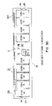
- FIGS. 4A and 4B together comprise a schematic view of the novel ECC/ Parity buffer chip 21 on DIMM 20 where, for clarity in description, it is shown as comprised of two distinct sections 21 a and 21 b.
- FIG. 4A shows the input portion of the enhanced function 4 rank-enabled 28 bit 1 : 2 buffer/register segment 21 a of the present invention and
- FIG. 4B shows the output portion and error correction code circuit segment 21 b.
- the buffer chip also referred to herein as the buffer device
- the error correction code circuit ECC segment 21 b shown in FIG.
- This ECC segment also includes a parity operating mode circuitry together and error reporting circuitry.
- the novel ECC/ Parity buffer 21 on DIMM 20 thus provides leading-edge performance and reliability and key operational features different from and unavailable from the prior art while retaining timing requirements generally consistent with devices such as the JEDEC 14 bit 1 : 2 DDR II register.
- the register segment 21 a contains a plurality of so called differential bit receivers 40 a through 40 e , 41 , 42 a through 42 n, 43 a , 43 b , 44 a , 44 b , 45 a , 45 b , 46 a and 46 b and a single amplifier 47 .
- Each of these differential receivers 40 a through 40 e , 41 , 42 a through 42 n , 43 a , 43 b , 44 a , 44 b , 45 a , 45 b , 46 a and 46 b has two inputs and a single output.
- each differential receiver 40 a through, 40 e , 41 , 42 a through 42 n , 43 a , 43 b , 44 a , 44 b , 45 a , 45 b , 46 a and 46 b is coupled to a reference voltage source 28 .
- the second input of the each of the differential receivers 40 a through, 40 e , 41 , 42 a through 42 n , 43 a , 43 b , 44 a , 44 b , 45 a , 45 b , 46 a and 46 b are coupled to respective inputs 30 a through, 30 e , 31 , 32 a through 32 n , 33 a , 33 b , 33 c , 33 d , 34 , 35 a , 35 b , 36 a and 36 b.
- Receiver set 40 a through 40 e is comprised of five receivers of which only the first and the last receivers 40 a and 40 e are shown.
- Receivers 40 a through 40 e have their second inputs respectively coupled to respective check bit lines 30 a through 30 e and their outputs connected through respective primary multiplexers 60 a through 60 e to the inputs of respective primary latches 70 a through 70 e.
- the check bit lines are contained in a bus that contains a set of five such check bit lines.
- FIG. 4A shows only the first and the last check bit lines 30 a and 30 e of the set and the first and last of the receivers 40 a through 40 e.
- each receiver in the set 40 a through 40 e has one of its respective inputs coupled to a respective one of a set of check bit input lines 30 a through 30 e and its output to a respective one of a set of three input multiplexers and thence to a respective one of a set of three input primary latches.
- the second input of the differential receiver 41 is coupled to a check bit 0 / Parity_ in signal line 31 .
- Receiver set 42 a through 42 n is comprised of twenty-two receivers coupled to a data line bus typically containing twenty two data lines 32 a through 32 n .
- FIG. 4 a shows only the first and the last data lines 32 a and 32 n of the set and the first and last of the receivers 42 a through 42 n are shown in the drawing.
- the first receiver 42 a is shown as having its first input coupled to data bit line 32 a and its output coupled to the first input of multiplexer 62 a whose output is coupled to a first input of primary latch 72 a and the last receiver 42 n is shown as having its first input coupled to data bit line 32 n and its output coupled to the first input of multiplexer 62 n whose output is coupled to a first input of primary latch 72 n.
- Each respective receiver in set 42 a through 42 n has an input coupled to a respective one of data lines in set 32 a through 32 n and their outputs connected through respective primary multiplexers 42 a through 42 n to the inputs of respective primary latches 62 a through 62 n.
- All the primary multiplexers and latches in the set 42 a through 42 n are identical to those shown connected to receivers 42 a and 42 n.
- each receiver in the set has one of its respective inputs coupled to a respective one of a set of data bit input lines and its output to a respective one of a set of two input multiplexers and thence to a respective one of a set of primary latches.
- These signals are inputted from the memory interface chip 18 in FIG. 2 and are re-driven only when one or more of the inputs 33 a , 33 b , or 34 are low.
- the second input of the differential receiver 41 is coupled to a check bit 0 /Parity_ in signal line 31 .
- the output of the differential receiver 41 is coupled to an input of multiplexer 61 whose output is coupled to a primary latch 71 .
- the check bit 0 /Parity_ in signal is interpreted as an ECC check bit from the memory controller or as a parity bit depending on the setting of ECC mode input 136 ( FIG. 4B )
- Clock inputs 131 are fed to all the primary latches 70 a through 70 e , 71 , 72 a through 72 n , 73 , 74 , 75 a , 75 b , 76 a and 76 b.
- the Check bits 1 - 5 at inputs 30 a through 30 e are in a don't care state when the register is being operated in parity mode and will be held low. When these inputs are operated in parity mode, a parity in signal will be provided on the Check bit 0 /Parity_ in signal line 31 and maintain odd parity across the data inputs 32 a through 32 n , at the rising edge of the clock signal (CK) at input 131 that immediately follows the rising edge of clock 131 that occurred simultaneously with the associated data inputs 32 a through 32 n.
- CK clock signal
- the second inputs of the differential receivers 43 a , 43 b , 44 a and 44 b are respectively coupled to chip select lines /CS 0 , /CS 2 , /CS 1 and /CS 3 and the outputs of the differential receivers 43 a and 44 a are coupled respectively to the first inputs of primary latches 73 and 74 as well as to the first and third inputs of a five input select NAND gate 63 , while the outputs of the differential receivers 43 b and 44 b are coupled only to the second and fourth inputs of the five input select NAND gate 63 .
- the output of NAND gate 63 is coupled to the selection input of the multiplexers 60 a through 60 e , 61 and 62 a through 62 n.
- This lines initiate DRAM address/command decodes and as such at least one will be low when a valid address/command signal is present and the register can be programmed to re-drive all the data inputs when at least one chip select input (/CS 0 , /CS 1 , /CS 2 , /CS 3 ) 33 a , 33 b , 33 c , 33 d is low.
- the fifth input of this NAND gate 63 is coupled to CS gate enable circuit 34 which can be set low to cause multiplexers 60 a through 60 e to pass signals from receivers 32 a through 32 n independent of the levels on inputs 33 a , 33 b , 33 c and 33 d.
- differential receivers 43 a and 44 a are also respectively coupled through the lines 172 and 174 and the AND gate 175 ( FIG. 4B ) whose output is coupled to the error logic circuit 100 also shown in FIG. 4 b.
- Receiver 45 a has an input coupled to the clock enable signal source 35 a (CKE 0 ) and an output coupled to the primary latch 75 a.
- Receiver 45 b has an input coupled to the clock enable signal sources 35 b (CKE 1 ) and an output coupled to the primary latch 75 b.
- Receiver 46 a has an input coupled to the on die termination line signal input line 36 a (ODT 0 ) and an output coupled to the primary latch 76 a.
- Receiver 46 b has an input coupled to the on die termination line signal line 36 b (ODT 1 ) and an output coupled to the primary latch 76 b.
- Receiver 47 has an input coupled to the reset (/RST) signal line 37 .
- the inputs 35 a and 35 b (CKE 0 , CKE 1 ) 36 a and 36 ba (ODT 0 , ODT 1 ) are provided from the memory interface chip 18 and are not associated with the Chip Select (CS) inputs 33 a , 33 b , 33 c and 33 d , and the signal from source 37 (/RST) driving amplifier 47 is an asynchronous reset input and, when low, resets all the primary latches 70 a through 70 e , 71 , 72 a through 72 n , 73 , 74 , 75 a , 75 b , 76 a , 76 b and all the secondary latches 92 a through 92 n , 93 , 94 , 95 a , 95 b , 96 a and 96 b thereby forcing the outputs low.
- This signal from source 37 (/RST) also resets
- module location identification is provided to error logic circuit 100 which is more fully described in conjunction with FIG. 6 below.
- This module location identification is provided to error logic circuit 100 through receivers 79 a , 79 b , and 79 c whose inputs are coupled to DIMM address input range sources (SA 0 , SA 1 , SA 2 ) 78 a , 78 b and 78 c and whose outputs are coupled to an error logic circuit 100 .
- the signals from sources (SA 0 , SA 1 , SA 2 ) 78 a , 78 b and 78 c define the DIMM address which is then reported on the error bus when requested by the system.
- This error logic circuit 100 is controlled by a signal from the NAND gate 175 when either of the DRAM chip select signal sources (/CS 0 ) 33 a and (/CS 1 ) 33 b are active.
- the error logic circuit 100 further has a reset signal source 180 coupled thereto.
- SEC/DED ECC circuit 90 which is more fully described in conjunction with FIG. 5 below. Coupled to this SEC/DED ECC circuit are the outputs of primary latches 70 a through 70 e , 71 and 72 a through 72 n.
- This SEC/DED ECC circuit 90 provides three outputs 109 , 110 , and 111 to the error logic circuit 100 . These outputs are: a correctable error (CE) line 109 , an uncorrectable error (UE) line 110 and a parity error bit line 111 fed to the error logic circuit 100 which provides outputs regarding correctable and uncorrectable errors on output lines 120 and 121 .
- CE correctable error
- UE uncorrectable error
- error line (CE) 109 or uncorrectable error line (UE) 110 When either error line (CE) 109 or uncorrectable error line (UE) 110 is low this indicates that an error was identified as being associated with the address and/or command inputs (either correctable or uncorrectable).
- the error lines 120 , 121 will be active, i.e., low, for two clock cycles simultaneous with the re-driven address/command data when operating in ECC mode or delayed by two clock cycles when operating in parity mode.
- the logic error circuit 100 also provides an Error Bus (Inter Integrated Circuit or IIC) 122 for external collection of error information such as error type, DIMM address, error count and status of the 28 input and internally generated syndrome bits at the time of the first fail. The information remains latched until a reset command is written to bus 122 or /RST input 37 is switched low.
- IIC Inter Integrated Circuit
- This SEC/DED ECC circuit 90 also has data bit outputs coupled through secondary latches 92 a through 92 n to a first input of all the output or secondary multiplexers 102 a through 102 n.
- the output of register latches 72 a through 72 n labeled BYPASS are directly connected to the second input of the output or secondary multiplexers 102 a through 102 n thereby allowing the SEC/DED ECC circuit 90 to be bypassed depending on the ECC mode input 123 .
- the output of the primary or register latches 73 , 74 , 75 a , 75 b , 76 a and 76 b are all coupled to a first input of secondary or output latches 93 , 94 , 95 a , 95 b , 96 a and 96 b and through these secondary latches 93 , 94 , 95 a , 95 b , 96 a and 96 b to a first input of output or secondary multiplexers 103 , 104 , 105 a , 105 b , 106 a and 106 b.
- the outputs of primary latches 73 , 74 , 75 a , 75 b , 76 a and 76 b are connected directly to a second input of output or secondary multiplexers 103 , 104 , 105 a , 105 b , 106 a and 106 b thereby allowing secondary latches 93 , 94 , 95 a , 95 b , 96 a and 96 b to be bypassed based on the /Delay CKE input 124 and /ECC mode input 123 .
- a control circuit comprised of a differential register 130 that has a first input coupled to a CK signal input 131 , a second input coupled to a /CK signal input 132 and its output coupled to a second input all the primary latches 70 a through 70 e , 71 , 72 a through 72 n , 73 , 74 , 75 a , 75 b , 76 a and 76 b and to the second input of all the output or secondary latches 92 a through 92 n , 93 , 94 , 95 a , 95 b , 96 a and 96 b and to the error logic circuit 100 via line 88 .
- the /ECC mode signal source 135 is coupled to a selection third input of secondary multiplexers 102 a through 102 n , 103 and 104 and to the error logic circuit 100 .
- the output or secondary multiplexers 105 a , 105 b , 106 a and 106 b have their selection inputs coupled to a source 124 of /Delay, CKE_ODT signals.
- the ECC code selected for this module is a single error correction/double error detection (SEC/DED) code and is shown in the H-Matrix depicted in FIG. 6 .
- SEC/DED single error correction/double error detection
- the present invention describes a unique DIMM having an enhanced 4 rank-enabled 28 bit 1 : 2 register with added error correction code logic (ECC) incorporated therein for correcting single bit errors while permitting continuous memory operation independent of the existence of these errors.
- ECC error correction code logic
- a parity operating mode is also provided, in conjunction with error reporting circuitry to permit the system to interrogate the device to determine the error condition.
- the above described 28 bit 1 : 2 register of the present invention provides key operational features, which differ from existing register designs intended for memory module applications and includes: 4 rank operability, disabling of un-needed internal circuitry when the module is not selected, error detection and correction on key inputs; programmable delay for un-gated inputs; parity mode; reset circuitry; error reporting and identification and reporting of the DIMM address.
- CS gating of key inputs is provided as a means of reducing device power for the internal latches which will only be updated and related internal circuitry utilized when one, two, three or all of the chip select CS) inputs are active low (and chip select gate enable tied high) at the rising edge of the system clock.
- the twenty-two chip select-gated signals associated with this function include addresses continuously re-driven at the rising edge of every clock depending on the state of chip select.
- the chip select gating function can be disabled by tying the chip select gate enable input low thereby enabling all internal latches to be updated on every rising edge of clock.
- the 4 rank circuitry in the enhanced 4-rank enabled ECC/parity buffer chip 21 is designed such that the enhanced 4-rank buffer device/chip 21 can be utilized as a direct replacement for earlier 2-rank enabled buffers, on one and two rank DIMMs, with no changes to the wiring of the assembly originally designed to use the earlier device.
- the inputs to differential receivers 43 b and 44 b are designed to float to a high level when not connected to an input source, the register pins assigned to inputs /CS 2 33 c and /CS 3 33 d were previously assigned to redundant VDD pins, and novel wiring on the 4 rank memory module depicted in FIGS. 3A-3D permit two of these buffers to be used on the 4-rank memory modules as shown in subsequent figures.
- ECC Mode For all inputs gated by CS, on-chip SEC/DED ECC logic is enabled and the signal received on CHK 0 /Parity in is received as check bit 0 when /ECC Mode input is low. This ECC logic will operate across 28 inputs (22 ‘CS-gated inputs and the 6 check bits) and will correct all single bit errors and detect all double bit errors present on the twenty-two chip select gated data inputs. If a correctable error is detected, /Error (CE) will be driven low for two clocks and errors will be counted and latched in the error bus registers for the 28 inputs if this is the first error since a reset is issued.
- CE Error
- any double bit error will also be detected (as well as many other errors that are not correctable), and will be reported on the /Error (UE) error line (driven low for two clocks) and in the error bus registers if this error is the first since a Reset is issued.
- UE /Error
- /CS 0 , /CS 1 , /CS 2 and /CS 3 are not included in the ECC logic, the propagation delay of the CS output signals will track the signals included in the ECC logic (1 additional clock of latency).
- the same twenty two chip select gated data signals can be operated in ‘parity mode (/ECC Mode high), whereby the signal received on CHK 0 /Parity in line is received as parity to the register one clock pulse later than the chip select gated data inputs. The received parity bit is then compared to the parity calculated across these same inputs by the register parity logic to verify that the information has not been corrupted.
- the twenty two chip select gated data signals will be latched and re-driven on the first clock pulse and any error will be reported two clock pulses later via the Uncorrectable Error (UE) line (driven low for two clock pulses) and in the Error Bus Registers. No correction of errors will be completed in this mode.
- the convention of parity, in this application, is odd parity (odd numbers of Is across data and parity inputs equals valid parity).
- the /RST signal input is used to clear all internal latches (including the error registers), and all outputs will be driven low quickly except the error lines which will be driven high.
- Error reporting circuitry is included to permit external monitoring of DIMM operation.
- /Error (CE) indicates that a correctable error occurred and was corrected by the ECC logic
- /Error (UE) indicates that an uncorrectable error occurred and depending on the mode selected is an uncorrectable ECC error or a parity error. Note that the timing of /Error (UE) is different in parity mode vs. ECC mode.
- an error bus (enabling access to 10 registers that can be read and reset via an IIC bus) is available to permit the device to be interrogated for additional error information, such as the error type (correctable, uncorrectable or parity error), error count and the memory card location (via the SAO-2 address pins which are conventionally wired only to the separate serial program decode (SPD) electronic erasable programmable read only memory (EE PROM).
- SPD serial program decode
- E PROM electronic erasable programmable read only memory
- CS chip select
- Other information is also available for diagnostics such as the signals received by the register (address/command, control signals, check bits, parity bit) when a chip select (CS) is active low and the associated syndrome bits so that they can be decoded to determine which of the 28 input signals (22 ‘CS-gated plus 6 check bits) or internal ECC logic failed, as well as an indication of the buffer type (1 to 2 rank enabled buffer or 1 to 4 rank enabled buffer), the buffer die revision, an indication of the buffer vendor, the maximum buffer speed, the driver strength and whether ECC has been bypassed by the application or not.
- These registers will contain information about the first fail, and the error counter will continue to increment until it is reset or reaches the full count (64K). All registers can be reset by writing the reset error bus command on the IIC bus, or via the /RST pin.
- each of these contacts is provided with a first contact on a first side of the DIMM and a redundant contact directly opposite the first contact and/or offset by no more than two pins from the first contact on the opposite side of the DIMM.
- the voltage reference source 28 is applied via contact or pin 1 on the front side of the DINM it is also applied via contact or pin 139 on the back side of the DIMM with contact 1 being direct opposite contact 139 .
- the SDA signal is applied via contact or pin 135 on the front side of the DIMM and also via the contact or pin 273 on the back side of the DIMM and the /CS 3 signal is applied via contact or pin 89 on the front side of the DIMM and also via contact or pin 225 on the back side of the DIMM.
- FIGS. 7A , 7 B and 7 C A full description of the contact or pin assignment matrix for the present invention is shown in FIGS. 7A , 7 B and 7 C.
- the specific contact placement is selected to maximize fault tolerance.
- problems caused, for example, by a slight bowing of the DIMM will cause low contact pressure on a contact on one side of DIMM but high pressure on the opposing contact. In such cases good signal flow will always be assured when such redundant and opposing contacts, as discussed above, are used.
- These opposing and redundant contacts will also facilitate board wiring by minimizing wiring congestion for this solution also permits in-line wiring.
- the following chart is a listing of the DIMM locations of a few of these contacts.
- the ECC function adds a single clock pulse delay (at planned operating frequencies) to the DIMM register performance, which may be of concern to some performance-optimized applications.
- two additional modes are included on the module that permit the system user to tradeoff performance and reliability.
- Parity Mode the memory interface chip or controller would generate a single parity bit in conjunction with providing the full address and command field to the module.
- the module would re-drive the address and command bits, to the DRAMs, in the next cycle—rather than adding the additional cycle required in ECC mode. Any error on the address and command bus would be reported to the system at a later time, and the potential for recovery from the fail would be small hence this option is undesirable for many applications.
- the last mode would be to simply operate the memory in a mode with no parity bits and no ECC bits, with neither the added delay due to ECC nor any means to detect a fault on the address/command bus as per the prior art convention now used for these modules.
- FIG. 5 is a block diagram of the SEC/DED ECC circuit of FIG. 4B .
- the twenty-two data inputs 32 a through 32 n via the twenty two latches 72 a through 72 n and lines 82 a through 82 n are fed both to a check bit generator circuit 230 and a first input of a parity generator/checker circuit 231 .
- the parity generator/checker circuit 231 further has a second input coupled to the parity in signal source 31 via primary latch 71 and output line 81 and depending on the state of the parity input signal on input 31 sends a parity error signal (PERR) on output line 111 to the error logic circuit 100 .
- PERR parity error signal
- check bit generator circuit 230 is transferring the twenty two inputted data signals to a first input of a syndrome bit generator 232 whose second input is coupled to the check bit inputs 30 a through 30 e through the lines 80 a through 80 e coming from the primary latches 70 a through 70 e.
- the Syndrome bit generator 232 then transfers the twenty two data signals to a first input of a syndrome bit decoder and the six check bits to the error generator 235 which determines if there are either correctable or uncorrectable errors in the received data and provides the appropriate correctable error or uncorrectable error signal to the error logic circuit 100 via either line 109 or 110 .
- the syndrome bit decoder now decodes the twenty-two data bits and transfers them to the data correction circuit 234 .
- the syndrome bits are selectively Xored with the data inputs consistent with the H-matrix, shown in FIG. 6 , with any single bit errors in the data field inverted to correct the error.
- the Error Logic block 100 consists of 3 major elements (not shown) which are an error counter, a status register block that contains a plurality of status registers, and an IIC logic block all of which are interconnected through common logic circuits. All of these blocks as well as the interconnecting logic circuits are common and readily available circuits known to those skilled in the art.
- the error counter is a 16-bit counter that increments as it receives errors inputs (CE, UE or Parity) from the SEC/DED ECC 90 . This error counter continues to count errors (until it reaches its full count) even while the status registers are being read out on the IIC bus.
- the status register block includes, in the present case, ten eight bit register sets (0-9) which contain information on the data input (DO- 21 ) signals, the check bit signals (CO- 5 and Parity In) signals received from the memory controller 19 , as well as signals from the memory module 20 (FCC/Parity Mode, SA 0 - 2 ), the error count, and the syndrome bits (S 0 - 5 ) which are calculated by the SEC/DED ECC 90 .
- the ten eight bit registers include an indication of the buffer type (1 to 2 rank enabled buffer or 1 to 4 rank enabled buffer), the buffer die revision, an indication of the buffer vendor, the maximum buffer speed, the driver strength and whether ECC has been bypassed by the application or not.
- the IIC Logic block includes the necessary logic to support the “IIC Bus Specifications Version 2.1 January 2000 Standard”.
- the register is an IIC slave where the register is addressed by the DIMM address input range sources (SA 0 , SA 1 , SA 2 ) 78 a , 78 b and 78 c and responds to several IIC bus commands—reset, read from the ten (10) Status Registers and the test mode.
- the miscellaneous logic circuits interconnecting the above described error counter, status register block and IIC logic block include logic circuits designed to reset the error counters and the ten (10) status registers from either the external reset signal (/RST) source 37 or an internal power-on reset, to load the contents of the ten status registers and logic (including a set of shadow registers) that the IIC logic will send out onto the IIC bus when a IIC bus read occurs, along with some control logic to drive the correctable error (CE) and uncorrectable error (UE) lines out if such an error occurs.
- CE correctable error
- UE uncorrectable error
- the error bus that provides access to the ten ( 10 ) internal status registers (that can be read and reset via an IIC bus) permits the device to be interrogated for additional error information, such as the error type (correctable, uncorrectable or parity error), error count and the memory card location (via the SA 0 - 2 address pins, also shared by the separate SPD EPROM). Other information is also available for diagnostics such as the signals received by the register (address/command, control signals, check bits, parity bit) associated with a CS is active low and the syndrome bits so that they can be decoded to determine, in the case of a failure, which of the 28 input signals (22 ‘CS-gated plus 6 check bits) failed.
- additional error information such as the error type (correctable, uncorrectable or parity error), error count and the memory card location (via the SA 0 - 2 address pins, also shared by the separate SPD EPROM).
- Other information is also available for diagnostics such as the signals received by the register (address/command, control signals,
- the ten eight bit registers further include an indication of the buffer type (1 to 2 rank enabled buffer or 1 to 4 rank enabled buffer), the buffer die revision, an indication of the buffer vendor, the maximum buffer speed, the driver strength and whether ECC has been bypassed by the application or not. These registers will contain information about the first fail, and the error counter will continue to increment until it is reset or reaches the full count (64K). All registers can be reset by writing the Reset Error Bus command on the IIC bus.
- the Byte 0 Status Register is the general status bit register that can be read to determine the type of error, the mode and the address of the DIMM (same as the DIMM SPD address).
- Bytes 1 and 2 Error Counter.
- the 16 bit error counter will count up to 64K errors (FFFF hex) based on any error (CE, UE or Parity Error).
- Byte 1 is the LSB and byte 2 is the MSB of the error counter. Once the 16-bit counter has counted up to all ones, it will stay all Is until the error bus is reset. The error counter register will not increment during a IIC read operation but will continue to count errors if they occur.
- Bytes 3 - 7 show the polarity of all 28 signals of the addresses and commands plus the check bits and parity bit that were received at the time of the first fail.
- Byte 3 Data Register A (DO–7) Bit 7 Bit 6 Bit 5 Bit 4 Bit 3 Bit 2 Bit 1 Bit 0 D7 D6 D5 D4 D3 D2 D1 D0 Byte 4: Data Register B (D8–15) Bit 7 Bit 6 Bit 5 Bit 4 Bit 3 Bit 2 Bit 1 Bit 0 D15 D14 D13 D12 D11 D10 D9 D8 Byte 5: Data Register C (D16–21, CSO–1) Bit 7 Bit 6 Bit 5 Bit 4 Bit 3 Bit 2 Bit 1 Bit 0 CS1 CS0 D21 D20 D19 D18 D17 D16 Byte 6: Data Register D (CKE0–1, ODT0–1, CS2–3) Bit 7 Bit 6 Bit 5 Bit 4 Bit 3 Bit 2 Bit 1 Bit 0 RFU RFU CS3 CS2 ODT1 ODT0 CKE1 CKE0 0 0 0 0 0 Byte 7: Check Bit (CO–5) and Parity Register Bit 7 Bit 6 Bit 5 Bit 4 Bit 3 Bit 2 Bit 1 Bit 0 RFU RFU Check
- Byte 8 Syndrome Register. Byte 8 shows the syndrome bits associated with the first error. These can be decoded to determine which of the 22 ‘CS-gated signals or 6 Check Bits caused the fail. Bytes 3 - 7 show the polarity of all input signals at the time of the fail. FIG. 8 shows the timing diagram used with the present invention.
- Byte 8 Syndrome Bit (0–5) Register Bit 7 Bit 6 Bit 5 Bit 4 Bit 3 Bit 2 Bit 1 Bit 0 RFU RFU Syndrome Syndrome Syndrome Syndrome Syndrome Syndrome 0 0 Bit 5 Bit 4 Bit 3 Bit 2 Bit 1 Bit 0
- Byte 9 provides operational information such as bit 7 , which indicates whether ECC checking is active and bit 6 , which indicates the drive strength setting for the drivers, at the time the register contents are interrogated.
- bit 9 provides useful information regarding the buffer device such as bit 5 (the maximum clock speed that the buffer is intended to operate at), the supplier (the exemplary embodiment allows two suppliers to be uniquely identified via a pre-defined bit assignment), although the use of bit 4 or an additional byte (i.e. byte 10 ) would permit the unique identification of 4 or more suppliers), and the supplier's die revision (the exemplary embodiment permits unique identification of up to 8 die revisions).
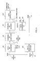
- FIG. 9 depicts a variety of configurations that may be implemented using the enhanced 4-rank enabled buffer chip 21 described herein. As shown in FIG. 9 , the buffer chip 21 may be utilized on existing memory modules that support one or two ranks of memory devices, thereby eliminating the need to upgrade to new memory modules to utilize the enhanced 4-rank enabled buffer chip 21 . In addition, FIG. 9 depicts two of the enhanced 4-rank enabled buffer chips 21 being utilized on a high density 4 rank memory module to access the 4 ranks of memory devices.
- a one buffer chip configuration 902 is depicted in FIG. 9 as an interconnect drawing showing the interconnections between the enhanced 4-rank enabled buffer chip 21 and the EPROM 302 (shown as VPD (Vital Product Data) but could also be used to contain SPD, or Serial Presence Detect information) on an exemplary memory module having 9 eight bit wide or 18 four or eight bit wide memory devices and a single 4-rank enabled buffer chip 21 .
- outputs from the buffer chip 21 include an indication of whether the error is a correctable error (CE) or an uncorrectable error (UE) as well as the corrected (if error is correctable) command and address information, which connect to memory devices 22 .
- CE correctable error
- UE uncorrectable error
- the internal status registers (bytes 0 through 9 ) of the buffer chip 21 can be accessed via an IIC bus by operating the SCL and SDA pins that connect to the buffer ( 2 , 140 and 2 , 141 respectively) consistent with the IIC Bus Specification.
- SCL data clock
- SDA IIC data input
- a two buffer chip configuration 904 is depicted in FIG. 9 as an interconnect drawing showing the interconnections between the enhanced 4-rank enabled buffer chips 21 and the EPROM 302 on an exemplary memory module having 36 four bit wide memory devices and two 4-rank enabled buffer chips 21 .
- the CS 2 and CS 3 inputs are disconnected, and thus, the enhanced 4-rank enabled buffer chip 21 can operate on a standard, prior art, one or two rank memory module without requiring a system upgrade.
- the status registers in buffer 1 can be separately accessed from the status registers in buffer 2 due to the fact that the SA 2 pin on buffer 1 is tied to ground, whereas the SA 2 pin on buffer 2 is tied to Vdd.
- the SA 0 and SA 1 inputs for both buffers are connected to the SA 0 and SA 1 pins on the module, resulting in the two buffers having unique addresses.
- up to 4 modules, each with 2 buffers can be installed in a system that permits independent addressing of the status registers in the 8 total buffer devices (using a unique SA 0 and SA 1 input combination for each of the four module positions in conjunction with the SA 2 wiring shown).
- a two buffer chip configuration 906 is depicted in FIG. 9 as an interconnect drawing showing the interconnections between the enhanced 4-rank enabled buffer chips 21 and the EPROM 302 on an exemplary memory module having 72 four bit wide memory devices and two 4-rank enabled buffer chips 21 .
- the buffer one has a CS 0 signal connected to the CS 0 pin and a CS 1 signal connected to the CS 1 pin
- register two has a CS 2 signal connected to the CS 0 pin and a CS 3 signal connected to the CS 1 pin.
- the enhanced buffer chips 21 described herein may be utilized in a first mode with existing memory modules that support one or two ranks of memory devices and in a second mode with high density memory modules that support four ranks of memory devices with up to 72 memory devices.
- the second mode is executed when two buffer chips 21 are coupled together on a memory module with all four of the chip selects (CS 0 , CS 1 , CS 2 and CS 3 ) being utilized to access different ranks of memory devices.
- the enhanced buffer chips 21 include 2 additional chip select input lines, but continue to perform the same functions, have the same pin counts, and have the same outputs as prior art buffer devices, therefore, the enhanced buffer chips 21 can be interchanged with prior art buffer devices by disconnecting the 2 additional chip select input lines.
- FIG. 10 is an interconnect drawing showing an exemplary embodiment of the chip select wiring at the inputs and outputs of the enhanced 4-rank buffer chip 21 when used on a memory module that supports up to four ranks of memory devices.
- Two buffer chips 21 are required in this exemplary embodiment to drive all of the DRAM devices at the intended operating frequencies.
- buffer chip 21 a accesses the first and second rank (CS 0 and CS 1 ) of memory devices located on the left and right sides of the memory module and buffer chip 21 b accesses the third and fourth rank (CS 2 and CS 3 ) of memory devices located on the left and right sides of the memory module
- the exemplary buffer includes two copies of each chip select output, with one copy (e.g.
- the DRAMs 1002 are wired such that each of the two buffers drive one copy of each chip select (e.g. “/CSx”) output to 10 DRAMs located to one side of the buffer and 8 DRAMs located to the other side of the buffer and on the same side of the buffer as the first DRAMs ( 18 DRAMs in total).
- each chip select e.g. “/CSx”
- the buffer driving /CS 2 and /CS 3 is located on the front of the DIMM, and the buffer driving /CS 0 and /CS 1 is located on the back of the DIMM.
- Alternate exemplary embodiments may swap the location of the buffers, or may re-drive /CS 0 and /CS 2 in one buffer device and /CS 1 and CS 3 in a second buffer device, while not straying from the teachings described herein.
- Address and command wiring is fully described in the text associated with FIGS. 3A-3D .
- the wiring to the chip select inputs of buffer chip 21 b is swapped between CS 0 / 1 and CS 2 / 3 .
- the buffer chip 21 is operable with as few as one rank of memory devices (e.g., with only one chip select input line being selectable) and as many as four ranks of memory devices (e.g., with all four chip select input lines being selectable).
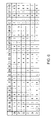
- FIG. 11 is a table describing the IIC addressing associated with the one or more buffer chips 21 utilized in memory modules implementing exemplary embodiments, when either one or two registers, or buffer chips 21 , are installed on a given memory module.
- the SA 2 is hard-wired on two and four rank memory modules so that the internal status registers can be read from each buffer chip 21 , as previously described.
- column 1102 is the slot in the memory system being occupied by the memory module and column 1104 is the binary IIC address associated with the memory module slot in column 1102 .
- the IIC address correlates to the slot being occupied by the memory module as shown in column 1106 .
- memory modules having one or two ranks of memory and a single buffer chip 21 can be installed in up to eight system module slots, whereas memory modules having up to four ranks of memory devices are limited to up to four memory system module slots, due to such factors as the bus loading on the data bus, overall system power, unique addressability of the internal registers of the buffer devices, etc. This limitation may not hold true in all applications, but is applicable in the exemplary embodiment described herein.
- the invention also provides a means for and a method for adjusting the propagation delay for signals on the memory module that are not included in the ECC circuitry such that the signals can be selectively re-driven within one or two clock cycles. This results in a significant increase in module operating speed.
- unused ECC check bit inputs can be held at a low level, i.e., “0” thus ensuring that these inputs are at a known and quiescent state.
- the present invention is an enhanced function 4 rank-enabled 28 bit 1 : 2 buffer/register, intended for use on main memory modules having one to four ranks of memory devices.
- the buffer includes addressability for up to 4 ranks of memory devices and includes ECC logic to correct single bit errors and permit continuous memory operation independent of the existence of these errors.
- a parity operating mode is also provided, in conjunction with error reporting circuitry to permit the system to interrogate the device to determine the error condition.
- the present invention also provides CS gating of key inputs through the use of CS 0 , CS 1 , CS 2 , CS 3 and CS Gate Enable.
- the buffer's internal latches will only be updated when one or more of the CS inputs are active low (and CS Gate Enable at a high level) at the rising edge of clock.
- the 22 ‘CS-gated signals associated with this function include addresses (addr 0 : 15 , BA 0 : 2 ).
- the CS gating function can be disabled by tying CS Gate Enable low enabling all internal latches to be updated on every rising edge of clock.
- a delay block can be selected to re-align the timing relationships which are offset by one clock cycle when the error correction code is enabled.
- the on-chip SEC/DED ECC logic is enabled and the signal received on CHK 0 /Parity In is received as check bit 0 via a programming pin (/ECC Mode low).
- This ECC logic will operate across 28 inputs (22 CS-gated inputs and the 6 check bits), and will correct all single bit errors present on the 22 CS-gated inputs.
- /Error (CE) will be driven low for two clocks and errors will be counted and latched in the Error Bus Registers for the 28 inputs.
- Any double bit error will also be detected (as well as any error that is not correctable), and will be reported on the /Error (UE) error line (driven low for two clocks) and in the Error Bus Registers.
- UE Error
- CS 0 - 3 are not included in the ECC logic, the propagation delay of the CS output signals will track the signals included in the ECC logic (1 additional clock of latency).
- the same 22 CS-gated signals can be operated in ‘parity mode (/ECC Mode high), whereby the signal received on CHK 0 /Parity In is received as parity to the register 1 clock later than the ‘CS-gated inputs. The received parity bit is then compared to the parity calculated across these same inputs by the register parity logic to verify that the information has not been corrupted.
- the 22 ‘CS-gated signals will be latched and re-driven on the first clock and any error will be reported two clocks later via the /Error (UE) line (driven low for two clocks) and in the Error Bus Registers. No correction of errors will be completed in this mode.
- the convention of parity is odd parity (odd numbers of 1's across data and parity inputs equals valid parity).
- the /RST pin is used to clear all internal latches (including the error registers), and all outputs will be driven low quickly except the error lines which will be driven high.
- the error reporting circuitry of the present invention is included to permit external monitoring of device operation.
- /Error (CE) indicates that a correctable error occurred and was corrected by the ECC logic.
- /Error (UE) indicates that an uncorrectable error occurred and depending on the mode selected is an uncorrectable ECC error or a parity error. Note that the timing of UE is different in parity mode vs ECC mode.
- the error bus (the ten registers discussed above that can be read and reset via an IIC bus) is available to permit the device to be interrogated for additional error information, such as the error type (correctable, uncorrectable or parity error), error count and the memory card location (via the SA 0 - 2 address pins, also shared by the separate SPD EPROM).
- additional error information such as the error type (correctable, uncorrectable or parity error), error count and the memory card location (via the SA 0 - 2 address pins, also shared by the separate SPD EPROM).
- Other information is also available for diagnostics such as the signals received by the register (address/command, control signals, check bits, parity bit) when a CS is active low and the syndrome bits so that they can be decoded to determine which of the 28 input signals (22 CS-gated plus 6 check bits) failed.
- These registers will contain information about the first fail, and the error counter will continue to increment until it is reset or reaches the full count (64K). All registers can be reset
- the memory controller(s) may be integrated together with one or more processor chips and supporting logic, packaged in a discrete chip (commonly called a “northbridge” chip), included in a multi-chip carrier with the one or more processors and/or supporting logic, or packaged in various alternative forms that best match the application/environment. Any of these solutions may or may not employ one or more narrow/high speed links to connect to one or more hub chips and/or memory devices.
- the memory modules may be implemented by a variety of technology including a DIMM, a single in-line memory module (SIMM) and/or other memory module or card structures.
- a DIMM refers to a small circuit board which is comprised primarily of random access memory (RAM) integrated circuits or die on one or both sides with signal and/or power pins on both sides of the board.
- RAM random access memory
- SIMM which is a small circuit board or substrate composed primarily of RAM integrated circuits or die on one or both sides and single row of pins along one long edge.
- the DIMM depicted in FIG. 1 includes 276 pins in the exemplary embodiment, whereas DIMMs can be constructed with other pincounts while still retaining the same functionality as that described herein.
- Memory devices are generally defined as integrated circuits that are composed primarily of memory (storage) cells, such as DRAMs (Dynamic Random Access Memories), SRAMs (Static Random Access Memories), FeRAMs (Ferro-Electric RAMs), MRAMs (Magnetic Random Access Memories), Flash Memory and other forms of random access and related memories that store information in the form of electrical, optical, magnetic, biological or other means.
- DRAMs Dynamic Random Access Memories
- SRAMs Static Random Access Memories
- FeRAMs Fero-Electric RAMs
- MRAMs Magnetic Random Access Memories
- Flash Memory and other forms of random access and related memories that store information in the form of electrical, optical, magnetic, biological or other means.
- Dynamic memory device types may include asynchronous memory devices such as FPM DRAMs (Fast Page Mode Dynamic Random Access Memories), EDO (Extended Data Out) DRAMs, BEDO (Burst EDO) DRAMs, SDR (Single Data Rate) Synchronous DRAMs, DDR (Double Data Rate) Synchronous DRAMs or any of the expected follow-on devices such as DDR 2 , DDR 3 , DDR 4 and related technologies such as Graphics RAMs, Video RAMs, LP RAM (Low Power DRAMs) which are often based on the fundamental functions, features and/or interfaces found on related DRAMs.
- FPM DRAMs Fast Page Mode Dynamic Random Access Memories
- EDO Extended Data Out
- BEDO Back EDO
- SDR Single Data Rate
- DDR Double Data Rate Synchronous DRAMs
- DDR Double Data Rate Synchronous DRAMs or any of the expected follow-on devices
- Memory devices may be utilized in the form of chips (die) and/or single or multi-chip packages of various types and configurations.
- the memory devices may be packaged with other device types such as other memory devices, logic chips, analog devices and programmable devices, and may also include passive devices such as resistors, capacitors and inductors.
- These packages may include an integrated heat sink or other cooling enhancements, which may be further attached to the immediate carrier or another nearby carrier or heat removal system.
- Module support devices may be comprised of multiple separate chips and/or components, may be combined as multiple separate chips onto one or more substrates, may be combined onto a single package or even integrated onto a single device—based on technology, power, space, cost and other tradeoffs.
- one or more of the various passive devices such as resistors, capacitors may be integrated into the support chip packages, or into the substrate, board or raw card itself, based on technology, power, space, cost and other tradeoffs.
- These packages may include an integrated heat sink or other cooling enhancements, which may be further attached to the immediate carrier or another nearby carrier or heat removal system.
- Memory devices, buffers, registers, clock devices, passives and other memory support devices and/or components may be attached to the memory subsystem via various methods including solder interconnects, conductive adhesives, socket structures, pressure contacts and other methods which enable communication between the two or more devices via electrical, optical or alternate means.
- the one or more memory modules may be connected to the memory system, processor complex, computer system or other system environment via one or more methods such as soldered interconnects, connectors, pressure contacts, conductive adhesives, optical interconnects and other communication and power delivery methods.
- Connector systems may include mating connectors (male/female), conductive contacts and/or pins on one carrier mating with a male or female connector, optical connections, pressure contacts (often in conjunction with a retaining mechanism) and/or one or more of various other communication and power delivery methods.
- the interconnection(s) may be disposed along one or more edges of the memory assembly and/or placed a distance from an edge of the memory subsystem depending on such application requirements as ease-of-upgrade/repair, available space/volume, heat transfer, component size and shape and other related physical, electrical, optical, visual/physical access, etc.
- the term memory subsystem refers to, but is not limited to: one or more memory devices; one or more memory devices and associated interface and/or timing/control circuitry; and/or one or more memory devices in conjunction with a memory buffer, and/or switch.
- the term memory subsystem may also refer to one or more memory devices, in addition to any associated interface and/or timing/control circuitry and/or a memory buffer assembled into a substrate, a card, a module or related assembly, which may also include a connector or similar means of electrically attaching the memory subsystem with other circuitry.
- the memory modules described herein may also be referred to as memory subsystems because they include one or more memory devices and buffers.
- Memory subsystem support device(s) may be directly attached to the same substrate or assembly onto which the memory device(s) are attached, or may be mounted to a separate interposer or substrate also produced using one or more of various plastic, silicon, ceramic or other materials which include electrical, optical or other communication paths to functionally interconnect the support device(s) to the memory device(s) and/or to other elements of the memory or computer system.
- Signals may include such methods as single-ended, differential, optical or other approaches, with electrical signaling further including such methods as voltage or current signaling using either single or multi-level approaches.
- Signals may also be modulated using such methods as time or frequency, non-return to zero, phase shift keying, amplitude modulation and others. Voltage levels are expected to continue to decrease, with 1.5V, 1.2V, 1V and lower signal voltages expected consistent with (but often independent of) the reduced power supply voltages required for the operation of the associated integrated circuits themselves.
- One or more clocking methods may be utilized within the memory subsystem and the memory system itself, including global clocking, source-synchronous clocking, encoded clocking or combinations of these and other methods.
- the clock signaling may be identical to that of the signal lines themselves, or may utilize one of the listed or alternate methods that is more conducive to the planned clock frequency(ies), and the number of clocks planned within the various subsystems.
- a single clock may be associated with all communication to and from the memory, as well as all clocked functions within the memory subsystem, or multiple clocks may be sourced using one or more methods such as those described earlier.
- the functions within the memory subsystem may be associated with a clock that is uniquely sourced to the subsystem, or may be based on a clock that is derived from the clock related to the information being transferred to and from the memory subsystem (such as that associated with an encoded clock). Alternately, a unique clock may be used for the information transferred to the memory subsystem, and a separate clock for information sourced from one (or more) of the memory subsystems.
- the clocks themselves may operate at the same or frequency multiple of the communication or functional frequency, and may be edge-aligned, center-aligned or placed in an alternate timing position relative to the data, command or address information.
- Information passing to the memory subsystem(s) will generally be composed of address, command and data, as well as other signals generally associated with requesting or reporting status or error conditions, resetting the memory, completing memory or logic initialization and other functional, configuration or related information.
- Information passing from the memory subsystem(s) may include any or all of the information passing to the memory subsystem(s), however generally will not include address and command information.
- Initialization of the memory subsystem may be completed via one or more methods, based on the available interface busses, the desired initialization speed, available space, cost/complexity objectives, subsystem interconnect structures, the use of alternate processors (such as a service processor) which may be used for this and other purposes, etc.
- the high speed bus may be used to complete the initialization of the memory subsystem(s).
- Another initialization method might utilize a distinct bus, such as a presence detect bus (such as the one defined in U.S. Pat. No. 5,513,135 to Dell et al., of common assignment herewith), an IIC bus (such as defined in published JEDEC standards such as the 168 Pin DIMM family in publication 21-C revision 7R8) and/or the SMBUS, which has been widely utilized and documented in computer systems using such memory modules.
- a presence detect bus such as the one defined in U.S. Pat. No. 5,513,135 to Dell et al., of common assignment herewith
- an IIC bus such as defined in published JEDEC standards such as the 168 Pin DIMM family in publication 21-C revision 7R8
- SMBUS which has been widely utilized and documented in computer systems using such memory modules.
- This bus might be connected to one or more modules within a memory system in a point-to-point, multi-drop, daisy chain/cascade interconnect or alternate structure, providing an independent means of interrogating memory subsystems, programming each of the one or more memory subsystems to operate within the overall system environment, and adjusting the operational characteristics at other times during the normal system operation based on performance, thermal, configuration or other changes desired or detected in the system environment.
- the integrity of the communication path, the data storage contents and all functional operations associated with each element of a memory system or subsystem can be assured, to a high degree, with the use of one or more fault detection and/or correction methods described herein.
- Any or all of the various elements may include error detection and/or correction methods such as CRC (Cyclic Redundancy Code), EDC (Error Detection and Correction), parity or other encoding/decoding methods suited for this purpose.
- Further reliability enhancements may include operation re-try (to overcome intermittent faults such as those associated with the transfer of information), the use of one or more alternate or replacement communication paths to replace failing paths and/or lines, complement-re- complement techniques or alternate methods used in computer, communication and related systems.
- bus termination on busses as simple as point-to-point links or as complex as multi-drop structures, is becoming more common consistent with increased performance demands.
- a wide variety of termination methods can be identified and/or considered, and include the use of such devices as resistors, capacitors, inductors or any combination thereof, with these devices connected between the signal line and a power supply voltage or ground, a termination voltage or another signal.
- the termination device(s) may be part of a passive or active termination structure, and may reside in one or more positions along one or more of the signal lines, and/or as part of the transmitter and/or receiving device(s).
- the terminator may be selected to match the impedance of the transmission line, or selected via an alternate approach to maximize the useable frequency, operating margins and related attributes within the cost, space, power and other constraints.
- the embodiments of the invention may be embodied in the form of computer-implemented processes and apparatuses for practicing those processes.
- Embodiments of the invention may also be embodied in the form of computer program code containing instructions embodied in tangible media, such as floppy diskettes, CD-ROMs, hard drives, or any other computer-readable storage medium, wherein, when the computer program code is loaded into and executed by a computer, the computer becomes an apparatus for practicing the invention.
- the present invention can also be embodied in the form of computer program code, for example, whether stored in a storage medium, loaded into and/or executed by a computer, or transmitted over some transmission medium, such as over electrical wiring or cabling, through fiber optics, or via electromagnetic radiation, wherein, when the computer program code is loaded into and executed by a computer, the computer becomes an apparatus for practicing the invention.
- computer program code segments configure the microprocessor to create specific logic circuits.
Abstract
Description
- This invention relates generally to a high-density, high-reliability memory module with a fault tolerant address and command bus for use as a main memory that will achieve the degree of fault-tolerance and self-healing necessary for autonomic computing systems.
- Memory modules are well known to the prior art and have been and are presently being used in practical applications such as in computers and other equipment using solid state memories.
- Broadly speaking, currently available main memories offer bandwidths in the range of 1.6 to 2.6 GB/s, and although some memories provide for limited data path error correction most offer no means of any error correction targeting the interface between the memory controller and the memory subsystem. Furthermore, memory modules for server products and other higher-end computing systems usually include re-drive logic for address and command inputs, and clock re-synchronization and re-drive circuitry associated with the memory subsystems to permit these modules to contain higher memory device counts and to ensure accurate clock timings at each device on the memory assembly. Although these solutions provide systems with the ability to achieve the specified bandwidth objectives, the overall quantity and types of failures in the memory subsystem, outside the data path itself, has actually increased due to the added circuitry associated with each memory device. Simultaneously, as these computing systems are more widely utilized in business, many applications simply cannot accept periodic unplanned system outages caused by failed memory modules. Thus the emphasis and need for improved overall system reliability is increasing dramatically and requires a comprehensive system solution that includes both a high degree of fault tolerance and overall reliability. Further, a corresponding need for greater system memory density is also required to achieve the system performance and operation throughput required in modem business applications, as well as to maximize the return on investment by extending the utility of the system by offering memory density improvements.
- The present invention provides such a comprehensive system solution that includes the capability of high memory density and a high degree of fault tolerance and the overall differentiated system reliability long desired in the server market.
- Existing solutions have memory module density that is typically limited to 18 or 36 devices for each memory module—with this limit based on such elements as the memory device package size, the memory module physical dimensions, the re-drive capability of the buffer, re-drive or register device, the power dissipation of the completed memory subsystem and/or module, etc. Other possible fault-tolerant improvement methods such as memory mirroring, symbol slicing and extensive forms of fault rejection and redundancy, provide enhanced memory subsystem reliability, but, due to negative impacts such as increased cost, power, and reduced performance, have been considered only for niche applications where price is not of high importance as these subsystem quality enhancements are very expensive to implement. Therefore solutions suitable for the low or midrange server markets have not been available.
- Consequently the industry has long sought a simple, relatively inexpensive and reliable solution that provides high memory density with differentiated product quality, that provides an adequate level of asset-protection that does not endanger the reliability of the system through the use of reduced-finction memory assemblies and yet is cost competitive.
- The present invention is directed to a high density high reliability memory controller/interface module, provided with a high degree of compatibility with industry-standard solutions, capable of meeting the desired density, performance and reliability requirements and interfacing with the presently available memory modules, as well as with existing or enhanced support devices. The present invention accomplishes all these ends, resulting in a high density and enhanced reliability memory solution at low cost.
- An object of the present invention is to provide an enhanced 28 bit 1:2 register (also referred to herein as a “buffer”) that supports 4 ranks of memory devices, intended for use with memory subsystems such as Dual Inline Memory Modules (DIMMs) having Dynamic Random Access Memory (DRAM) chips thereon. The register of the present invention has added thereto additional command inputs, error correction code (ECC) logic to identify and correct single bit errors on the command or address bus, and permit continuous memory operation independent of the existence of these errors.
- Another object of the present invention is to include in such DIMMs error latches and an error reporting mode whereby the system may interrogate the device to determine the error condition thereby allowing accurate fault determination and preventive maintenance—thereby reducing unplanned system outages.
- A further object of the present invention is to include redundant contacts on all connectors/DIMM interconnects that would otherwise be considered single points of failure whereby an intermittent or permanent contact failure would result in an unplanned system outage.
- Still another object of the present invention is to provide the DIMM with key operational features such as chip select gating of key inputs and programmable delay for un-gated inputs, thereby reducing module power and offering increased operational flexibility.
- A further object of the present invention is to provide a DIMM that can be readily utilized in presently available controllers in a manner most applicable to the market needs.
- Another further object of the present invention is to have a DIMM that uses connectors similar to those presently in use so that prior art contacts, molds, handlers and related production tools can continue to be used such that the modules can be more cheaply produced with additional density while providing value-added reliability, and other value-add attributes, such as a higher memory packaging density with minimal additional production costs.
- Another further object of the present invention is to have a buffer which is operable with up to 4 ranks of memory devices, that is also interchangeable with previously developed buffers limited to no more than 2 ranks of memory devices, and can be used as a direct replacement for said previously developed buffers on DIMMs that utilized said buffers—thereby eliminating the need to produce or procure two types of buffer devices or to re-design existing memory modules.
- The DIMM of the present invention is comprised of a printed circuit board having a front side and a back side and a plurality of double data rate (DDR) DRAMs or synchronous dynamic random access memories (SDRAMs) affixed to both the front surface and the back surface. On a first edge of the front surface of said board there is provided one hundred and thirty eight (138) contacts for connecting circuitry, external to the card, to the SDRAMS and related devices on the DIMM and on the same first edge on the rear side of the card there is provided an additional one hundred and thirty eight (138) external circuitry connecting contacts so that the board has a total of two hundred and seventy six (276) external circuitry connecting contacts thereon. The contact means provided on the front and the back sides of the printed circuit card provide for electrically connecting the external circuitry to the SDRAMs in a direct or indirect manner.
- Still another further object of the present invention is to provide a server memory structure having a dual inline memory module or DIMM provided with selective redundant contacts, a phase lock loop, 2 or 32K bit serial electronically erasable programmable read only memory (EE PROM) and a 28 bit, 1 to 2 register having error correction code (ECC), parity checking, a multi-byte fault reporting register, read via an independent bus, and real time error lines for both correctable errors and uncorrectable error conditions. More particularly the server of the present invention comprises a novel DIMM provided with a new and unique ECC/ Parity Register that is operable with 1 to 4 memory ranks, coupled to a memory interface chip which is in turn coupled to a memory controller or processor such that the memory controller sends address and command information to the buffer (or register) via address/command lines together with check bits for error correction purposes to the ECC/ Parity register.
- Still another object of the invention is to provide for detecting if the module installed in the server can monitor the address and control bus integrity, correct errors on the address and control bus, report errors and log and counts errors.
- Still another object of the invention is to provide for Parity error reporting in which the parity signal is delivered one cycle after the address and command to which it applies, and the error line be driven low two clocks after the address and command bits are driven to the DRAMs from the register on the DIMM. After holding the error line low for only 2 clock cycles, the driver can be disabled and the output permitted to return to an un-driven state (high impedance) thus allowing this line to be shared by multiple modules.
- Still further the invention provides means for and a method for adjusting the propagation delay, for signals on the memory module that are not included in the ECC circuitry, such that the signals can be selectively re-driven by the buffer within one or two clock cycles.
- Still further the present invention permits operation of the memory module in parity mode, such that unused ECC check bit inputs are held at a low level thus ensuring that these inputs are at a known and quiescent state.
- Still further the present invention provides for reducing the probability of Single Point of Failures occurring by providing selected signals with redundant contacts directly on the opposite side of the DIMM from the original finction contact thereby reducing the probability of a contact failure resulting in an unplanned system outage.
- Still further the present invention provides for operating a module of the present invention consistent with conventional non-ECC protected modules, by removing the secondary registers (post-ECC) from the delay path by setting the /ECC Mode control pin to a high level.
- These objects, features and advantages of the present invention will be become further apparent to those skilled in the art from the following detailed description taken in conjunction with the accompanying drawings wherein:
-
FIG. 1 is a block diagram of a typical server memory arrangement; -
FIG. 2 is a block diagram of the enhanced server memory arrangement of the present invention; -
FIGS. 3A and 3B are plan views respectively of the front and back of the two hundred and seventy six (276) pin dual inline memory module (DIMM) of the present invention that utilizes up to 72 planar DRAMS; andFIGS. 3C and 3D are plan views respectively of the front and back of the 276 pin DIMM of the present invention that utilizes up to eighteen four high DRAM stacks; -
FIGS. 4A and 4B are schematic views of the ECC/ Parity register, shown inFIG. 3A ; -
FIG. 5 is a block diagram of the single error correction/ double error detection error correction code (SEC/DED ECC) circuit ofFIG. 4B ; -
FIG. 6 describes, in H—matrix form, the preferred ECC code selected for the module ofFIG. 3 ; -
FIGS. 7A , 7B and 7C show the designated contacts or pin connections for the DIMM ofFIGS. 3A and 3B ; -
FIG. 8 shows the timing diagram used with the present invention; -
FIG. 9 shows the buffer connections and total number of buffers used in a system when the buffer of the present invention is used on 1, 2 and 4 rank DIMMs; -
FIG. 10 shows the CS wiring between the buffers and the memory devices on the right and left side of the card, for a 4 rank DIMM of the present invention; and -
FIG. 11 shows the IIC addresses that are utilized to access the error registers on the one or two buffers of the present invention. - A full appreciation of the features and advantages of the present invention can best be gained by reference to the drawings and more particularly to the figures where:
FIG. 1 is a block diagram of a typical server memory arrangement; FIG. 2 is a block diagram of the enhanced server memory arrangement of the present invention;FIGS. 3A and 3B are plan views respectively of the front and back of a 4 rank planar 276 contact dual inline memory module (DIMM) of the present invention;FIGS. 3C and 3D are plan views respectively of the front and back of a 4 rank four high stacked 276 contact DIMM of the present invention;FIGS. 4A and 4B are schematic views of the 4 rank-optimized buffer/register, parity and error correction circuits shown inFIGS. 3A and 3B (andFIGS. 3C and 3D );FIG. 5 is a block diagram of the single error correction/double error detection error correction code (SEC/DED ECC) circuit ofFIG. 4B ;FIG. 6 describes, in H—matrix, form the preferred ECC code selected for the module ofFIGS. 3A and 3C ;FIGS. 7A , 7B and 7C show the designated pin connections for the DIMM ofFIGS. 3A and 3B (andFIGS. 3C and 3D ).FIG. 8 shows the timing diagram used with the present invention.FIG. 9 shows the buffer connections and total number of buffers used in a system when the buffer of the present invention is used on 1, 2 and 4 rank DIMMs;FIG. 10 shows the CS wiring between the buffers and the memory devices on the right and left side of the card, for a 4 rank DIMM of the present invention andFIG. 11 is a table showing the IIC addresses that would be used to access the error registers on the one or two buffers of the present invention. - In
FIG. 1 there is illustrated, in schematic form, a block diagram of a typical server memory arrangement as might be found in any currently available server which can employ a plurality of memory subsystems, shown here in the form of dual inline memory modules (DIMMs). It should be understood that many such DIMMs would be used in actual practice but for ease of illustration only oneprior art DIMM 10 is shown inFIG. 1 .DIMM 10 is a printed circuit card on which there is provided a plurality of either synchronous dynamic random access memories or dynamic randomaccess memories circuits 11, herein after collectively referred to herein as memory devices, or as DRAM(s). EachDRAM 11 on theDIMM 10 has a plurality of input/output pins that are coupled, via the printed circuitry on theDIMM 10 to the contacts on theDIMM 10 and theses contacts are further coupled, via adata line 15, to amemory interface chip 18 and to a memory controller orprocessor 19. Each DRAM on the DIMM is further, coupled via such DIMM contacts, to a buffer/register 12 and to a phase lockedloop circuit 14 on the DIMM. The phase locked loop 14 (PLL) is connected viaclock line 17 to thememory interface chip 18. Theregister 12 is also coupled to thememory interface chip 18 via an address and command (CMD)bus 16. Thememory interface chip 18 is coupled to thememory controller 19 via thedata line 15, address andcommand line 16 andclock line 17. It should be understood that although only one such DIMM is shown in this figure that in actuality the server would contain many such DIMMs. Such other DIMMs would be coupled in a like manner to thememory interface chip 18 andmemory controller 19 via data, address and command lines, and may be connected in a multi-drop, cascade interconnect or other connection method, depending on the system structure and buffer functionality. Since such servers and their operation are well known to those skilled in the art, further description of such servers and their operation is not deemed necessary. - Turning now to
FIGS. 2 , 3A, 3B, 3C, 3D, 4A, 4B, 5, 8, 9, 10 and 11 the enhanced server memory arrangement of the present invention will be described. - In
FIG. 2 there is illustrated, in schematic form, a block diagram of a server memory arrangement employing the present invention. In thisFIG. 2 the server comprises anovel DIMM 20 provided with a novel ECC/Parity Buffer chip 21 (also referred to as a “buffer device”) coupled to thememory interface chip 18 which is in turn coupled to the memory controller orprocessor 19. It should be understood that thechip 21 need not include both the ECC function and the parity finction. For example, thechip 21 could have just the 4 rank addressability alone, the ECC finction alone or just the parity finction alone and still operate in accordance with the present invention. More specifically, as shown in thisFIG. 2 , thememory interface chip 18 sends and receives data from the DIMMs via thedata line 15 and sends address and commands vialine 16. Thememory interface chip 18 then sends and receives data, vialine 15, to the memory devices, orDRAMs 22 and sends address and command information to theregister chip 21 via add/cmd line 16 and check bits for error correction purposes to the ECC/Parity register chip 21 vialine 25. In this configuration, the check bits and/or parity bits associated with the ECC/Parity register chip 21 are developed in thememory interface chip 18, although in other embodiments these bits could be developed in the memory controller orprocessor 19, be communicated to the memory interface chip as a subset of the information online 16 and the memory interface would then re-drive this information to the memory module online 25. -
FIGS. 3A and 3B show respectively the front and back views of thenovel 4rank DIMM 20 of the present invention. Generally speaking DIMMs are printed circuit cards designed to carry a plurality ofDRAMs 22 thereon and the DRAM output pins (not shown) are connected via the printed circuit to selectedconnectors 23 along the edge of both the back and front sides of the card and are often provided with a single indexing key ornotch 9 on the connector edge. The use and manufacture of such DIMMs is well known and need not be further described herein. TheDIMM 20 of the present invention however is novel and is designed to address the need for very high memory module density, as well as several of the most significant contributors to unplanned and often catastrophic system outages encountered in the prior art DIMMs. The improvements in theDIMM 20 of the present invention are realized especially by enlarging the length ofDIMM 20 to between 149 mm and 153 mm. Nominally theDIMM 20 is 151.35 mm (5.97 inches) long and its width is 54.6 mm (2.16 inches). The width of theDIMM 20 is sufficient in width to accommodate the four rows ofDRAMs 22 installed thereon, in addition to the two buffers 21 (one buffer is mounted on each side in the exemplary embodiment, as shown inFIGS. 3A and 3B ), thePLL 24 and passive devices (not shown) such as resistors and capacitors, but must also be no wider than permitted by the available system physical dimensions for the module(s). The length of theDIMM 20 however must be such that theDIMM 20 can accommodate additional signal contacts, up to 138, as well as up to thirty-sixplanar DRAMs 26 having a nominal body size of up to 11.5 mm wide by 11 mm tall and have a locating key or notch 9 a distance of between 82.675 mm from one end of theDIMM 20 and 68.675 mm from the other end of the DIMM as shown. Again it should be understood that these dimensions are nominal and may vary plus or minus 3 mm in various implementations. TheDIMM 20 can also be provided with additional notches 9 a and 9 b on each side, i.e., the shorter edges of theDIMM 20. These dimensions permit the DIMM, of the invention, to accommodate placing up to thirty-sixplanar DRAMs 22 on the front surface and up to an additional thirty-sixsuch DRAMs 22 on the rear surface. Further, as shown inFIG. 3A , on the front of eachDIMM 20, in addition to the DRAMs, there is positioned a phase locked loop (PLL)chip 24 and the novel ECC/Parity Buffer chip 21 of the present invention. This novel ECC/Parity Buffer chip 21 will be further described below and in detail in conjunction withFIGS. 4A and 4B It should be understood that thePLL chip 24 can be eliminated if its circuitry is provided on thebuffer chip 21 or within the same package as the buffer chip 21 (i.e. alongside the chip, above the chip, below the chip, etc). In exemplary embodiments, theDIMM 20 depicted inFIGS. 3A and 3B also includes anEPROM 302 which is used for the storage of memory module attribute information (commonly referred to as an SPD data, when associated with memory modules), with the EPROM's IIC interface also shared, in this module, with the novel ECC/Parity Buffer chip, enabling one means for accessing status registers on the buffer chip(s). - Alternate configurations of the 4
rank DIMM 20 may be implemented by exemplary embodiments. See, for examplesFIGS. 3C and 3D which depict front and back plan views of a 4 rank four high stacked 276contact DIMM 20 of the present invention. In the embodiment depicted inFIG. 3D , theDIMM 20 also includes anEPROM device 302 which has the same function asdevice 302 in FIG. 3A, which includes enabling one means for accessing status registers on the buffer chip(s). As will be evident to those skilled in the art, other configurations for providing up to 4 ranks of memory may also be implemented without departing from the scope of the invention. For example, a 4 rank two high, stacked 276contact DIMM 20 may be implemented by exemplary embodiments. - This new, improved, larger
sized DIMM 20, shown in theseFIGS. 3A , 3B, 3C and 3D also achieves a further significant improvement in the interconnect failure rate for the larger size of the module permits the connector system to accommodate two hundred and seventy-six contacts or pins 23. These pins are numbered and coupled to respective inputs as shown inFIGS. 7 a, 7 b, and 7 c. Contact or pin number one (1) is identified and shown inFIG. 3A ascontact 23A and is on the left hand side of the front side of theDIMM 20 and is positioned approximately 5.175 mm from the left edge of theDIMM 20 and 77.5 mm from the center of thenotch 9. Contact or pin number one hundred and thirty-eight (138) is identified and shown inFIG. 3A ascontact 23B and is on the right hand side of the front side of theDIMM 20 and is positioned approximately 5.175 mm from the right edge of theDIMM 20 and approximately 63.5 mm from the center of thenotch 9. Contact or pin number one hundred and thirty-nine (139) is identified and shown inFIG. 3B ascontact 23C and is directly opposite contact number one 23A and is also positioned approximately 5.175 mm from the right edge of the back ofDIMM 20 and is also 77.5 mm from the center of thenotch 9. Contact or pin number two hundred and seventy-six (276) is identified in shown inFIG. 3B ascontact 23D and is directly opposite contact number one hundred and thirty-eight 23B and is also positioned approximately 5.175 mm from the left edge of the back ofDIMM 20 and 63.5 mm from the center of thenotch 9. The greater size of thisDIMM 20 also accommodates the inclusion of a new and larger ECC/Parity buffer chip 21 required by the present invention. Because the two hundred and seventy-six contacts or pins 23 on thislarger DIMM 20 are more than sufficient to meet the needs of all the circuitry on theDIMM 20 this means that theDIMM 20 provides extra or redundant contacts. These extra or redundant contacts or pins 23 can now be used to provide additional protection for certain selected signal or voltage lines, for which error correction is not possible. The present invention, by providing such redundant contacts, effectively eliminates concerns such as contact failures on clock inputs, CS, CKE, and ODT inputs, Vref inputs, and other signals not protected by ECC. Other benefits include the elimination or reduction of concerns regarding power supply noise and/or voltage drops due to scarcity of voltage (VDD) contacts in the data region as well providing additional ground pins in the address/ control region on theDIMM 20. The larger contact count of the present invention also permits theDIMM 20 to be wired such that they are consistent with prior art DIMMs. Theadditional contacts 23 also permit the inclusion of ECC check bits, associated with address and command inputs, allowing for real-time system monitoring of faults associated with these inputs, as well as system interrogation of fault counts and attributes. These faults would result in catastrophic system outages in conventional prior art systems using the smaller prior art DIMMs. - It should be understood that although only one
DIMM FIGS. 1 and 2 that, in actuality, the server would contain many such DIMMs. As noted above, theDIMM 20, of the present invention, is provided with a plurality ofSDRAMs 22, a phase lockedloop circuit 24 and the ECC/Parity buffer chips 21. The ECC/Parity buffer chips 21 onDIMM 20 include unique error correction code (ECC) circuitry that is coupled to thememory interface chip 18 vialine 25 to provide even greater significant reliability enhancement to such servers. The inclusion of this new, improved error correction code (ECC) circuitry results in a significant reduction in interconnect failure.Memory interface chip 18 connects to both of the ECC/Parity buffer chips 21 throughlines PLL 24 through line (17). In exemplary embodiments, such as the one depicted inFIGS. 3A and 3B , one copy of the address and command outputs frombuffer chip 21 located on the front of theDIMM 20 connect to the 20 (S)DRAMs to the left of the buffer chip 21 (10 DRAMs on the front and 10 DRAMs located behind said 10 DRAMs on the back of the DIMM), and the second copy connect to the 16 DRAMs to the right of the buffer (8 DRAMs on the front and 8 DRAMs located behind said 8 DRAMs on the back of the DIMM). Thebuffer chip 21 located on the back of the DIMM is wired in a similar manner, with one copy of the address and command outputs from the buffer connected to 20 DRAMs (10 on the front and 10 on the back) and a second copy connected to 16 DRAMs (8 on the front and 8 on the back). In exemplary embodiments, such as the one depicted inFIGS. 3C and 3D , one copy of the address and command outputs frombuffer chip 21 located on the front of theDIMM 20 connect to the 20 DRAMs to the left of the buffer (2 DRAM stacks on the front and 3 DRAM stacks generally located behind said 2 DRAM stacks on the back of the DIMM), and the second copy connects to the 20 DRAMs to the left of the buffer (3 DRAM stacks on the front and to the right of the buffer and 2 DRAM stacks located generally behind said 3 DRAM stacks on the back of the DIMM). Thebuffer chip 21 located on the back of the DIMM is wired in a similar manner, with one copy of the address and command outputs from the buffer connected to 16 DRAMs to the right (2 DRAM stacks on the front and 2 DRAM stacks on the back) and a second copy connected to 16 DRAMs to the right (2 DRAM stacks on the front and 2 DRAM stacks on the back).PLL 24 connects to each of theSDRAMs 22. - In an exemplary embodiment, a first set of buffer chip outputs connect to the SDRAM devices placed directly to the right of a
buffer chip 21 on the front side of theDIMM 20 and to the memory devices on the backside of theDIMM 20 and on the same end of theDIMM 20 as the aforementioned memory devices, and a second set of buffer outputs connect to the devices to the left of the buffer on the front side of theDIMM 20 and to the memory devices, orSDRAMS 22, on the backside of theDIMM 20 and on the same end of theDIMM 20 as these memory devices. Alternate exemplary wiring embodiments may be used, while achieving the benefits described herein. For example, inFIGS. 3A-3D , address and command outputs frombuffer 21, located on the front of the DIMM, may wire only to (S)DRAMs located on the front of the DIMM, while address and command outputs frombuffer 21, located on the back of the DIMM, may wire only to (S)DRAMs located on the back of the DIMM. Other wiring methods may be used for address and command, while achieving many of the objectives cited in the teachings. -
FIGS. 4A and 4B together comprise a schematic view of the novel ECC/Parity buffer chip 21 onDIMM 20 where, for clarity in description, it is shown as comprised of twodistinct sections FIG. 4A shows the input portion of theenhanced function 4 rank-enabled 28 bit 1:2 buffer/register segment 21 a of the present invention andFIG. 4B shows the output portion and error correctioncode circuit segment 21 b. As depicted inFIGS. 4A and 4B , the buffer chip (also referred to herein as the buffer device) includes a plurality of buffer circuits (e.g., receivers, multiplexers, latches, etc.) for driving the address and command data. The error correction codecircuit ECC segment 21 b, shown inFIG. 4B , corrects for single bit errors and thus permits continuous memory operation independent of the existence of these errors. This ECC segment also includes a parity operating mode circuitry together and error reporting circuitry. The novel ECC/Parity buffer 21 onDIMM 20 thus provides leading-edge performance and reliability and key operational features different from and unavailable from the prior art while retaining timing requirements generally consistent with devices such as theJEDEC 14 bit 1:2 DDR II register. - More particularly, the
register segment 21 a contains a plurality of so calleddifferential bit receivers 40 a through 40 e, 41, 42 a through 42n, 43 a, 43 b, 44 a, 44 b, 45 a, 45 b, 46 a and 46 b and asingle amplifier 47. Each of thesedifferential receivers 40 a through 40 e, 41, 42 a through 42 n, 43 a, 43 b, 44 a, 44 b, 45 a, 45 b, 46 a and 46 b has two inputs and a single output. One of the inputs of eachdifferential receiver 40 a through, 40 e, 41, 42 a through 42 n, 43 a, 43 b, 44 a, 44 b, 45 a, 45 b, 46 a and 46 b is coupled to areference voltage source 28. The second input of the each of thedifferential receivers 40 a through, 40 e, 41, 42 a through 42 n, 43 a, 43 b, 44 a, 44 b, 45 a, 45 b, 46 a and 46 b are coupled torespective inputs 30 a through, 30 e, 31, 32 a through 32 n, 33 a, 33 b, 33 c, 33 d, 34, 35 a, 35 b, 36 a and 36 b. - Receiver set 40 a through 40e is comprised of five receivers of which only the first and the
last receivers Receivers 40 a through 40 e have their second inputs respectively coupled to respectivecheck bit lines 30 a through 30 e and their outputs connected through respectiveprimary multiplexers 60 a through 60 e to the inputs of respectiveprimary latches 70 a through 70 e. Typically the check bit lines are contained in a bus that contains a set of five such check bit lines. However, for simplification of the drawing and ease of description only,FIG. 4A shows only the first and the lastcheck bit lines receivers 40 a through 40 e. It being understood that each receiver in the set 40 a through 40 e has one of its respective inputs coupled to a respective one of a set of check bitinput lines 30 a through 30 e and its output to a respective one of a set of three input multiplexers and thence to a respective one of a set of three input primary latches. - The second input of the
differential receiver 41 is coupled to acheck bit 0/ Parity_ insignal line 31. - Receiver set 42 a through 42 n is comprised of twenty-two receivers coupled to a data line bus typically containing twenty two
data lines 32 a through 32 n. However, for simplification of the drawing and ease of description only,FIG. 4 a shows only the first and thelast data lines receivers 42 a through 42 n are shown in the drawing. Thefirst receiver 42 a is shown as having its first input coupled to data bitline 32 a and its output coupled to the first input ofmultiplexer 62 a whose output is coupled to a first input ofprimary latch 72 a and thelast receiver 42 n is shown as having its first input coupled to data bitline 32 n and its output coupled to the first input ofmultiplexer 62 n whose output is coupled to a first input ofprimary latch 72 n. Each respective receiver in set 42 a through 42 n has an input coupled to a respective one of data lines inset 32 a through 32 n and their outputs connected through respectiveprimary multiplexers 42 a through 42 n to the inputs of respectiveprimary latches 62 a through 62 n. All the primary multiplexers and latches in the set 42 a through 42 n are identical to those shown connected toreceivers memory interface chip 18 inFIG. 2 and are re-driven only when one or more of theinputs - As previously noted, the second input of the
differential receiver 41 is coupled to acheck bit 0/Parity_ insignal line 31. The output of thedifferential receiver 41 is coupled to an input ofmultiplexer 61 whose output is coupled to aprimary latch 71. Thecheck bit 0/Parity_ in signal is interpreted as an ECC check bit from the memory controller or as a parity bit depending on the setting of ECC mode input 136 (FIG. 4B )Clock inputs 131 are fed to all the primary latches 70 a through 70 e, 71, 72 a through 72 n, 73, 74, 75 a, 75 b, 76 a and 76 b. The Check bits 1-5 atinputs 30 a through 30 e are in a don't care state when the register is being operated in parity mode and will be held low. When these inputs are operated in parity mode, a parity in signal will be provided on theCheck bit 0/Parity_ insignal line 31 and maintain odd parity across thedata inputs 32 a through 32 n, at the rising edge of the clock signal (CK) atinput 131 that immediately follows the rising edge ofclock 131 that occurred simultaneously with the associateddata inputs 32 a through 32 n. - The second inputs of the
differential receivers differential receivers primary latches select NAND gate 63, while the outputs of thedifferential receivers select NAND gate 63. The output ofNAND gate 63 is coupled to the selection input of themultiplexers 60 a through 60 e, 61 and 62 a through 62 n. These lines initiate DRAM address/command decodes and as such at least one will be low when a valid address/command signal is present and the register can be programmed to re-drive all the data inputs when at least one chip select input (/CS0, /CS1, /CS2, /CS3) 33 a, 33 b, 33 c, 33 d is low. The fifth input of thisNAND gate 63 is coupled to CS gate enablecircuit 34 which can be set low to causemultiplexers 60 a through 60 e to pass signals fromreceivers 32 a through 32 n independent of the levels oninputs - The output of
differential receivers lines FIG. 4B ) whose output is coupled to theerror logic circuit 100 also shown inFIG. 4 b. -
Receiver 45 a has an input coupled to the clock enablesignal source 35 a (CKE0) and an output coupled to theprimary latch 75 a. -
Receiver 45 b has an input coupled to the clock enablesignal sources 35 b (CKE1) and an output coupled to theprimary latch 75 b. -
Receiver 46 a has an input coupled to the on die termination linesignal input line 36 a (ODT0) and an output coupled to theprimary latch 76 a. -
Receiver 46 b has an input coupled to the on die terminationline signal line 36 b (ODT1) and an output coupled to theprimary latch 76 b. -
Receiver 47 has an input coupled to the reset (/RST)signal line 37. Theinputs memory interface chip 18 and are not associated with the Chip Select (CS)inputs amplifier 47 is an asynchronous reset input and, when low, resets all the primary latches 70 a through 70 e, 71, 72 a through 72 n, 73, 74, 75 a, 75 b, 76 a, 76 b and all the secondary latches 92 a through 92 n, 93, 94, 95 a, 95 b, 96 a and 96 b thereby forcing the outputs low. This signal from source 37 (/RST) also resets the error bus registers and error lines from theerror logic circuit 100. - Coupled to the above described register of
FIG. 4A is the unique error correction code circuit arrangement ofFIG. 4B . - In
FIG. 4B , module location identification is provided to errorlogic circuit 100 which is more fully described in conjunction withFIG. 6 below. This module location identification is provided to errorlogic circuit 100 throughreceivers error logic circuit 100. The signals from sources (SA0, SA1, SA2) 78 a, 78 b and 78 c define the DIMM address which is then reported on the error bus when requested by the system. Thiserror logic circuit 100 is controlled by a signal from theNAND gate 175 when either of the DRAM chip select signal sources (/CS0) 33 a and (/CS1) 33 b are active. Theerror logic circuit 100 further has areset signal source 180 coupled thereto. - Also included in the error correction code circuit of
FIG. 4B is a SEC/DED ECC circuit 90 which is more fully described in conjunction withFIG. 5 below. Coupled to this SEC/DED ECC circuit are the outputs ofprimary latches 70 a through 70 e, 71 and 72 a through 72 n. This SEC/DED ECC circuit 90 provides threeoutputs error logic circuit 100. These outputs are: a correctable error (CE)line 109, an uncorrectable error (UE)line 110 and a parityerror bit line 111 fed to theerror logic circuit 100 which provides outputs regarding correctable and uncorrectable errors onoutput lines logic error circuit 100 also provides an Error Bus (Inter Integrated Circuit or IIC) 122 for external collection of error information such as error type, DIMM address, error count and status of the 28 input and internally generated syndrome bits at the time of the first fail. The information remains latched until a reset command is written tobus 122 or /RST input 37 is switched low. The selected IIC protocol allows unique byte addressing of the ten registers, consistent with the present industry standard protocol for serial program decode electronic erasable programmable read only memory (SPD EPROM) and is well known to the art. - This SEC/
DED ECC circuit 90 also has data bit outputs coupled through secondary latches 92 a through 92 n to a first input of all the output orsecondary multiplexers 102 a through 102 n. The output of register latches 72 a through 72 n labeled BYPASS are directly connected to the second input of the output orsecondary multiplexers 102 a through 102 n thereby allowing the SEC/DED ECC circuit 90 to be bypassed depending on theECC mode input 123. - The output of the primary or register latches 73, 74, 75 a, 75 b, 76 a and 76 b are all coupled to a first input of secondary or output latches 93, 94, 95 a, 95 b, 96 a and 96 b and through these
secondary latches secondary multiplexers primary latches secondary multiplexers secondary latches Delay CKE input 124 and /ECC mode input 123. - A control circuit comprised of a
differential register 130 that has a first input coupled to aCK signal input 131, a second input coupled to a /CK signal input 132 and its output coupled to a second input all the primary latches 70 a through 70 e, 71, 72 a through 72 n, 73, 74, 75 a, 75 b, 76 a and 76 b and to the second input of all the output or secondary latches 92 a through 92 n, 93, 94, 95 a, 95 b, 96 a and 96 b and to theerror logic circuit 100 vialine 88. The /ECCmode signal source 135 is coupled to a selection third input ofsecondary multiplexers 102 a through 102 n, 103 and 104 and to theerror logic circuit 100. The output orsecondary multiplexers source 124 of /Delay, CKE_ODT signals. - The ECC code selected for this module is a single error correction/double error detection (SEC/DED) code and is shown in the H-Matrix depicted in
FIG. 6 . The use of this SEC/DED code ensures that all single errors associated with the address and command bits are detected and corrected and that all double bit errors are detected. It should be noted that interconnect failures almost exclusively begin as single point fails, with other failures possibly occurring over time dependent or independent of the root cause of the initial fail. - In summary, the present invention describes a unique DIMM having an enhanced 4 rank-enabled 28 bit 1:2 register with added error correction code logic (ECC) incorporated therein for correcting single bit errors while permitting continuous memory operation independent of the existence of these errors. A parity operating mode is also provided, in conjunction with error reporting circuitry to permit the system to interrogate the device to determine the error condition.
- The above described 28 bit 1:2 register of the present invention provides key operational features, which differ from existing register designs intended for memory module applications and includes: 4 rank operability, disabling of un-needed internal circuitry when the module is not selected, error detection and correction on key inputs; programmable delay for un-gated inputs; parity mode; reset circuitry; error reporting and identification and reporting of the DIMM address.
- CS gating of key inputs, e.g., /CS0, /CS1, /CS2 and /CS3, is provided as a means of reducing device power for the internal latches which will only be updated and related internal circuitry utilized when one, two, three or all of the chip select CS) inputs are active low (and chip select gate enable tied high) at the rising edge of the system clock. The twenty-two chip select-gated signals associated with this function include addresses continuously re-driven at the rising edge of every clock depending on the state of chip select. However, the chip select gating function can be disabled by tying the chip select gate enable input low thereby enabling all internal latches to be updated on every rising edge of clock.
- In exemplary embodiments, the 4 rank circuitry in the enhanced 4-rank enabled ECC/
parity buffer chip 21 is designed such that the enhanced 4-rank buffer device/chip 21 can be utilized as a direct replacement for earlier 2-rank enabled buffers, on one and two rank DIMMs, with no changes to the wiring of the assembly originally designed to use the earlier device. The inputs todifferential receivers CS2 33 c and /CS3 33 d were previously assigned to redundant VDD pins, and novel wiring on the 4 rank memory module depicted inFIGS. 3A-3D permit two of these buffers to be used on the 4-rank memory modules as shown in subsequent figures. - Programmable delay for un-gated inputs (/Delay CKE-ODT) associated with CKE and ODT (DRAM signals), the inputs will be latched and re-driven on each rising edge of the clock signal (CLK,) independent of the state of the chip select (CS) signals. However, since some controllers may be designed with limited flexibility regarding latency for these signals vs. chip select (CS), address (Addr), row address strobe (RAS), column address strobe (CAS) and write enable (WE), a delay block can be selected to re-align the timing relationships which are offset by 1 clock when the error correction code circuitry (ECC) is enabled.
- ECC Mode (/ECC Mode low): For all inputs gated by CS, on-chip SEC/DED ECC logic is enabled and the signal received on CHK0/Parity in is received as
check bit 0 when /ECC Mode input is low. This ECC logic will operate across 28 inputs (22 ‘CS-gated inputs and the 6 check bits) and will correct all single bit errors and detect all double bit errors present on the twenty-two chip select gated data inputs. If a correctable error is detected, /Error (CE) will be driven low for two clocks and errors will be counted and latched in the error bus registers for the 28 inputs if this is the first error since a reset is issued. Any double bit error will also be detected (as well as many other errors that are not correctable), and will be reported on the /Error (UE) error line (driven low for two clocks) and in the error bus registers if this error is the first since a Reset is issued. Although /CS0, /CS1, /CS2 and /CS3 are not included in the ECC logic, the propagation delay of the CS output signals will track the signals included in the ECC logic (1 additional clock of latency). - In addition to the above ECC mode, the same twenty two chip select gated data signals can be operated in ‘parity mode (/ECC Mode high), whereby the signal received on CHK0/Parity in line is received as parity to the register one clock pulse later than the chip select gated data inputs. The received parity bit is then compared to the parity calculated across these same inputs by the register parity logic to verify that the information has not been corrupted. The twenty two chip select gated data signals will be latched and re-driven on the first clock pulse and any error will be reported two clock pulses later via the Uncorrectable Error (UE) line (driven low for two clock pulses) and in the Error Bus Registers. No correction of errors will be completed in this mode. The convention of parity, in this application, is odd parity (odd numbers of Is across data and parity inputs equals valid parity).
- The /RST signal input is used to clear all internal latches (including the error registers), and all outputs will be driven low quickly except the error lines which will be driven high.
- Error reporting circuitry is included to permit external monitoring of DIMM operation. Two open-drain outputs are available to permit multiple modules to share a common signal line for reporting an error that occurred during a valid command (/CS=low) cycle (consistent with the re-driven signals). These two outputs are driven low for two clocks to allow the memory controller time to sense the error. /Error (CE) indicates that a correctable error occurred and was corrected by the ECC logic, /Error (UE) indicates that an uncorrectable error occurred and depending on the mode selected is an uncorrectable ECC error or a parity error. Note that the timing of /Error (UE) is different in parity mode vs. ECC mode.
- In addition, an error bus (enabling access to 10 registers that can be read and reset via an IIC bus) is available to permit the device to be interrogated for additional error information, such as the error type (correctable, uncorrectable or parity error), error count and the memory card location (via the SAO-2 address pins which are conventionally wired only to the separate serial program decode (SPD) electronic erasable programmable read only memory (EE PROM). Other information is also available for diagnostics such as the signals received by the register (address/command, control signals, check bits, parity bit) when a chip select (CS) is active low and the associated syndrome bits so that they can be decoded to determine which of the 28 input signals (22 ‘CS-gated
plus 6 check bits) or internal ECC logic failed, as well as an indication of the buffer type (1 to 2 rank enabled buffer or 1 to 4 rank enabled buffer), the buffer die revision, an indication of the buffer vendor, the maximum buffer speed, the driver strength and whether ECC has been bypassed by the application or not. These registers will contain information about the first fail, and the error counter will continue to increment until it is reset or reaches the full count (64K). All registers can be reset by writing the reset error bus command on the IIC bus, or via the /RST pin. - In addition to the use of the ECC structure defined above (included in both the memory interface chip and the register on the DIMM), redundant contacts are included on the module pinout to effectively eliminate other possible SPOF (single-point-of-failure) contributors in the interconnect system. Contacts that cannot be protected by the ECC structure described above, for various reasons, include the following: voltage reference (Vref), Clocks, Chip Selects (CS), CKEs, ODTs, VSS /VDD contacts or pins, Error lines, data input on the IIC bus (SDA), data clock on the IIC bus (SCL) and related signals. In the present invention each of these contacts is provided with a first contact on a first side of the DIMM and a redundant contact directly opposite the first contact and/or offset by no more than two pins from the first contact on the opposite side of the DIMM. For example if the
voltage reference source 28 is applied via contact orpin 1 on the front side of the DINM it is also applied via contact or pin 139 on the back side of the DIMM withcontact 1 being directopposite contact 139. Similarly the SDA signal is applied via contact or pin 135 on the front side of the DIMM and also via the contact or pin 273 on the back side of the DIMM and the /CS3 signal is applied via contact or pin 89 on the front side of the DIMM and also via contact or pin 225 on the back side of the DIMM. A full description of the contact or pin assignment matrix for the present invention is shown inFIGS. 7A , 7B and 7C. The specific contact placement is selected to maximize fault tolerance. By providing such opposite redundant contacts, problems caused, for example, by a slight bowing of the DIMM will cause low contact pressure on a contact on one side of DIMM but high pressure on the opposing contact. In such cases good signal flow will always be assured when such redundant and opposing contacts, as discussed above, are used. These opposing and redundant contacts will also facilitate board wiring by minimizing wiring congestion for this solution also permits in-line wiring. The following chart is a listing of the DIMM locations of a few of these contacts. -
Nominal Contact or Side of Distance from Direction Signal PIN# DIMM Key from Key CS0 86 FRONT 11.495 mm RIGHT CS0 224 BACK 11.495 mm LEFT CS1 91 FRONT 16.495 mm RIGHT CS1 229 BACK 16.495 mm LEFT CKE0 65 FRONT 13.505 MM LEFT CKE0 203 BACK 13.505 mm RIGHT CKE1 62 FRONT 16.505 mm LEFT CKE1 200 BACK 16.505 mm RIGHT RAS 222 BACK 9.495 mm LEFT CAS 87 FRONT 12.495 mm RIGHT WE 84 FRONT 9.495 mm RIGHT CK0 77 FRONT 2.495 mm RIGHT CK0 215 BACK 2.495 mm LEFT CK0B 78 FRONT 3.495 mm RIGHT CK0B 216 BACK 3.495 mm LEFT - The ECC function adds a single clock pulse delay (at planned operating frequencies) to the DIMM register performance, which may be of concern to some performance-optimized applications. As such, two additional modes are included on the module that permit the system user to tradeoff performance and reliability. In Parity Mode, the memory interface chip or controller would generate a single parity bit in conjunction with providing the full address and command field to the module. The module would re-drive the address and command bits, to the DRAMs, in the next cycle—rather than adding the additional cycle required in ECC mode. Any error on the address and command bus would be reported to the system at a later time, and the potential for recovery from the fail would be small hence this option is undesirable for many applications. The last mode would be to simply operate the memory in a mode with no parity bits and no ECC bits, with neither the added delay due to ECC nor any means to detect a fault on the address/command bus as per the prior art convention now used for these modules.
-
FIG. 5 is a block diagram of the SEC/DED ECC circuit ofFIG. 4B . The twenty-twodata inputs 32 a through 32 n via the twenty twolatches 72 a through 72 n and lines 82 a through 82 n are fed both to a checkbit generator circuit 230 and a first input of a parity generator/checker circuit 231. The parity generator/checker circuit 231 further has a second input coupled to the parity insignal source 31 viaprimary latch 71 andoutput line 81 and depending on the state of the parity input signal oninput 31 sends a parity error signal (PERR) onoutput line 111 to theerror logic circuit 100. - Meanwhile the check
bit generator circuit 230 is transferring the twenty two inputted data signals to a first input of asyndrome bit generator 232 whose second input is coupled to thecheck bit inputs 30 a through 30 e through thelines 80 a through 80 e coming from the primary latches 70 a through 70 e. - The
Syndrome bit generator 232 then transfers the twenty two data signals to a first input of a syndrome bit decoder and the six check bits to theerror generator 235 which determines if there are either correctable or uncorrectable errors in the received data and provides the appropriate correctable error or uncorrectable error signal to theerror logic circuit 100 via eitherline data correction circuit 234. In the correction circuit the syndrome bits are selectively Xored with the data inputs consistent with the H-matrix, shown inFIG. 6 , with any single bit errors in the data field inverted to correct the error. - The
Error Logic block 100 consists of 3 major elements (not shown) which are an error counter, a status register block that contains a plurality of status registers, and an IIC logic block all of which are interconnected through common logic circuits. All of these blocks as well as the interconnecting logic circuits are common and readily available circuits known to those skilled in the art. - More specifically, the error counter is a 16-bit counter that increments as it receives errors inputs (CE, UE or Parity) from the SEC/
DED ECC 90. This error counter continues to count errors (until it reaches its full count) even while the status registers are being read out on the IIC bus. - The status register block includes, in the present case, ten eight bit register sets (0-9) which contain information on the data input (DO-21) signals, the check bit signals (CO-5 and Parity In) signals received from the
memory controller 19, as well as signals from the memory module 20 (FCC/Parity Mode, SA0-2), the error count, and the syndrome bits (S0-5) which are calculated by the SEC/DED ECC 90. In addition, the ten eight bit registers include an indication of the buffer type (1 to 2 rank enabled buffer or 1 to 4 rank enabled buffer), the buffer die revision, an indication of the buffer vendor, the maximum buffer speed, the driver strength and whether ECC has been bypassed by the application or not. - The IIC Logic block includes the necessary logic to support the “IIC Bus Specifications Version 2.1 January 2000 Standard”. In this case the register is an IIC slave where the register is addressed by the DIMM address input range sources (SA0, SA1, SA2) 78 a, 78 b and 78 c and responds to several IIC bus commands—reset, read from the ten (10) Status Registers and the test mode.
- The miscellaneous logic circuits interconnecting the above described error counter, status register block and IIC logic block include logic circuits designed to reset the error counters and the ten (10) status registers from either the external reset signal (/RST)
source 37 or an internal power-on reset, to load the contents of the ten status registers and logic (including a set of shadow registers) that the IIC logic will send out onto the IIC bus when a IIC bus read occurs, along with some control logic to drive the correctable error (CE) and uncorrectable error (UE) lines out if such an error occurs. - The error bus that provides access to the ten (10) internal status registers (that can be read and reset via an IIC bus) permits the device to be interrogated for additional error information, such as the error type (correctable, uncorrectable or parity error), error count and the memory card location (via the SA0-2 address pins, also shared by the separate SPD EPROM). Other information is also available for diagnostics such as the signals received by the register (address/command, control signals, check bits, parity bit) associated with a CS is active low and the syndrome bits so that they can be decoded to determine, in the case of a failure, which of the 28 input signals (22 ‘CS-gated
plus 6 check bits) failed. The ten eight bit registers further include an indication of the buffer type (1 to 2 rank enabled buffer or 1 to 4 rank enabled buffer), the buffer die revision, an indication of the buffer vendor, the maximum buffer speed, the driver strength and whether ECC has been bypassed by the application or not. These registers will contain information about the first fail, and the error counter will continue to increment until it is reset or reaches the full count (64K). All registers can be reset by writing the Reset Error Bus command on the IIC bus. - The Byte 0: Status Register is the general status bit register that can be read to determine the type of error, the mode and the address of the DIMM (same as the DIMM SPD address).
-
Byte 0: Status Register Bit 7 Bit 6Bit 5Bit 4Bit 3Bit 2Bit 1Bit 0Extended DIMM DIMM DIMM Mode Parity ECC error ECCerror Status Address Address Address 1= ECC Error 1= UE 1=CE Register SA2 SA1 SA0 0= Pty 1=PERR (If 1, see Byte 9) -
Bytes 1 and 2: Error Counter. The 16 bit error counter will count up to 64K errors (FFFF hex) based on any error (CE, UE or Parity Error).Byte 1 is the LSB andbyte 2 is the MSB of the error counter. Once the 16-bit counter has counted up to all ones, it will stay all Is until the error bus is reset. The error counter register will not increment during a IIC read operation but will continue to count errors if they occur. -
Byte 1 (LSB) Bit 7Bit 6Bit 5Bit 4Bit 3Bit 2Bit 1Bit 0E7 E6 E5 E4 E3 E2 E1 E0 Byte 2 (MSB) Bit 7Bit 6Bit 5Bit 4Bit 3Bit 2Bit 1Bit 0E15 E14 E13 E12 E11 E1O E9 E8 - Bytes 3-7 show the polarity of all 28 signals of the addresses and commands plus the check bits and parity bit that were received at the time of the first fail.
-
Byte 3: Data Register A (DO–7) Bit 7Bit 6Bit 5Bit 4Bit 3Bit 2Bit 1Bit 0D7 D6 D5 D4 D3 D2 D1 D0 Byte 4: Data Register B (D8–15) Bit 7Bit 6Bit 5Bit 4Bit 3Bit 2Bit 1Bit 0D15 D14 D13 D12 D11 D10 D9 D8 Byte 5: Data Register C (D16–21, CSO–1) Bit 7Bit 6Bit 5Bit 4Bit 3Bit 2Bit 1Bit 0CS1 CS0 D21 D20 D19 D18 D17 D16 Byte 6: Data Register D (CKE0–1, ODT0–1, CS2–3) Bit 7Bit 6Bit 5Bit 4Bit 3Bit 2Bit 1Bit 0RFU RFU CS3 CS2 ODT1 ODT0 CKE1 CKE0 0 0 0 0 Byte 7: Check Bit (CO–5) and Parity Register Bit 7 Bit 6Bit 5Bit 4Bit 3Bit 2Bit 1Bit 0RFU RFU Check Check Check Check Check Check 0 0 Bit 5Bit 4Bit 3Bit 2Bit 1Bit 0/Pty In - Byte 8: Syndrome Register.
Byte 8 shows the syndrome bits associated with the first error. These can be decoded to determine which of the 22 ‘CS-gated signals or 6 Check Bits caused the fail. Bytes 3-7 show the polarity of all input signals at the time of the fail.FIG. 8 shows the timing diagram used with the present invention. -
Byte 8: Syndrome Bit (0–5) Register Bit 7 Bit 6Bit 5Bit 4Bit 3Bit 2Bit 1Bit 0RFU RFU Syndrome Syndrome Syndrome Syndrome Syndrome Syndrome 0 0 Bit 5Bit 4Bit 3Bit 2Bit 1Bit 0 -
Byte 9 provides operational information such asbit 7, which indicates whether ECC checking is active andbit 6, which indicates the drive strength setting for the drivers, at the time the register contents are interrogated. Inaddition byte 9 provides useful information regarding the buffer device such as bit 5 (the maximum clock speed that the buffer is intended to operate at), the supplier (the exemplary embodiment allows two suppliers to be uniquely identified via a pre-defined bit assignment), although the use ofbit 4 or an additional byte (i.e. byte 10) would permit the unique identification of 4 or more suppliers), and the supplier's die revision (the exemplary embodiment permits unique identification of up to 8 die revisions). Through the use of the contents ofbyte 9, further information can be obtained regarding the buffer settings at the time of failure, after power-up or at any other time during operation. In addition, systems using the enhanced 4-rank buffer device will be able to electronically detect the supplier code, die revision and speed sort of the buffer devices in the system, without the need to physically inspect the devices, by interrogating the installed memory subsystems containing the subject buffer devices. - This offers a significant advantage should it be necessary to identify installed buffers if issues arise regarding the viability of the devices in stalled in a system in regard to manufacturing, reliability or related concerns subsequent to the assembly of the memory subsystems.
-
Byte 9: Extended Status Register Description Bit (0–6) Register Bit 7 Bit 6Bit 5Bit 4Bit 3Bit 2Bit 1Bit 0ECC DS Speed RFU Supplier Die Die Die Bypass 1= Lo Drv 1=800 1=Supplier Rev Rev Rev 1=Yes 0=Hi Drv 0=667 A 0=No 0-Supplier B - All the information necessary for one skilled in the art to design this
error logic block 100 is included in the H-Matrix shown inFIG. 6 where D0 through D21 refer to the data bits, C0 through C5 refer to the check bits and S0 through S5 refer to the syndrome bits. -
FIG. 9 depicts a variety of configurations that may be implemented using the enhanced 4-rank enabledbuffer chip 21 described herein. As shown inFIG. 9 , thebuffer chip 21 may be utilized on existing memory modules that support one or two ranks of memory devices, thereby eliminating the need to upgrade to new memory modules to utilize the enhanced 4-rank enabledbuffer chip 21. In addition,FIG. 9 depicts two of the enhanced 4-rank enabledbuffer chips 21 being utilized on ahigh density 4 rank memory module to access the 4 ranks of memory devices. - A one
buffer chip configuration 902 is depicted inFIG. 9 as an interconnect drawing showing the interconnections between the enhanced 4-rank enabledbuffer chip 21 and the EPROM 302 (shown as VPD (Vital Product Data) but could also be used to contain SPD, or Serial Presence Detect information) on an exemplary memory module having 9 eight bit wide or 18 four or eight bit wide memory devices and a single 4-rank enabledbuffer chip 21. As shown inconfiguration 902, outputs from thebuffer chip 21 include an indication of whether the error is a correctable error (CE) or an uncorrectable error (UE) as well as the corrected (if error is correctable) command and address information, which connect tomemory devices 22. The internal status registers (bytes 0 through 9) of thebuffer chip 21 can be accessed via an IIC bus by operating the SCL and SDA pins that connect to the buffer (2, 140 and 2, 141 respectively) consistent with the IIC Bus Specification. At the SA0-2 input pins a memory card location is specified. The IIC data clock (SCL) and IIC data input (SDA) query the status registers on thebuffer chip 21. As depicted inconfiguration 902, the CS2 and CS3 inputs are disconnected and thus, the enhanced 4-rank enabledbuffer chip 21 can operate on a standard, prior art, one or two rank memory module without requiring a system upgrade. - A two
buffer chip configuration 904 is depicted inFIG. 9 as an interconnect drawing showing the interconnections between the enhanced 4-rank enabledbuffer chips 21 and theEPROM 302 on an exemplary memory module having 36 four bit wide memory devices and two 4-rank enabled buffer chips 21. The CS2 and CS3 inputs are disconnected, and thus, the enhanced 4-rank enabledbuffer chip 21 can operate on a standard, prior art, one or two rank memory module without requiring a system upgrade. The status registers inbuffer 1 can be separately accessed from the status registers inbuffer 2 due to the fact that the SA2 pin onbuffer 1 is tied to ground, whereas the SA2 pin onbuffer 2 is tied to Vdd. The SA0 and SA1 inputs for both buffers are connected to the SA0 and SA1 pins on the module, resulting in the two buffers having unique addresses. Using this method, up to 4 modules, each with 2 buffers, can be installed in a system that permits independent addressing of the status registers in the 8 total buffer devices (using a unique SA0 and SA1 input combination for each of the four module positions in conjunction with the SA2 wiring shown). - A two
buffer chip configuration 906 is depicted inFIG. 9 as an interconnect drawing showing the interconnections between the enhanced 4-rank enabledbuffer chips 21 and theEPROM 302 on an exemplary memory module having 72 four bit wide memory devices and two 4-rank enabled buffer chips 21. As depicted inconfiguration 906, the buffer one has a CS0 signal connected to the CS0 pin and a CS1 signal connected to the CS1 pin, and register two has a CS2 signal connected to the CS0 pin and a CS3 signal connected to the CS1 pin. - As depicted in
FIG. 9 , theenhanced buffer chips 21 described herein may be utilized in a first mode with existing memory modules that support one or two ranks of memory devices and in a second mode with high density memory modules that support four ranks of memory devices with up to 72 memory devices. The second mode is executed when twobuffer chips 21 are coupled together on a memory module with all four of the chip selects (CS0, CS1, CS2 and CS3) being utilized to access different ranks of memory devices. Theenhanced buffer chips 21 include 2 additional chip select input lines, but continue to perform the same functions, have the same pin counts, and have the same outputs as prior art buffer devices, therefore, theenhanced buffer chips 21 can be interchanged with prior art buffer devices by disconnecting the 2 additional chip select input lines. -
FIG. 10 is an interconnect drawing showing an exemplary embodiment of the chip select wiring at the inputs and outputs of the enhanced 4-rank buffer chip 21 when used on a memory module that supports up to four ranks of memory devices. Twobuffer chips 21 are required in this exemplary embodiment to drive all of the DRAM devices at the intended operating frequencies. As depicted inFIG. 10 ,buffer chip 21 a accesses the first and second rank (CS0 and CS1) of memory devices located on the left and right sides of the memory module andbuffer chip 21 b accesses the third and fourth rank (CS2 and CS3) of memory devices located on the left and right sides of the memory module Although not shown in this figure, the exemplary buffer includes two copies of each chip select output, with one copy (e.g. CS0A) wiring to the first rank ofDRAMs 1002 on the right side of the DIMM and the second copy (e.g. CS0B) wiring to the first rank ofDRAMs 1002 on the left side of the DIMM. In the exemplary embodiment for the module shown inFIGS. 3A and 3B , theDRAMs 1002 are wired such that each of the two buffers drive one copy of each chip select (e.g. “/CSx”) output to 10 DRAMs located to one side of the buffer and 8 DRAMs located to the other side of the buffer and on the same side of the buffer as the first DRAMs (18 DRAMs in total). In the exemplary embodiment for the module ofFIGS. 3A and 3B , the buffer driving /CS2 and /CS3 is located on the front of the DIMM, and the buffer driving /CS0 and /CS1 is located on the back of the DIMM. Alternate exemplary embodiments may swap the location of the buffers, or may re-drive /CS0 and /CS2 in one buffer device and /CS1 and CS3 in a second buffer device, while not straying from the teachings described herein. Address and command wiring is fully described in the text associated withFIGS. 3A-3D . Note that in this exemplary embodiment, the wiring to the chip select inputs ofbuffer chip 21 b is swapped between CS0/1 and CS2/3. As depicted inFIG. 10 , thebuffer chip 21 is operable with as few as one rank of memory devices (e.g., with only one chip select input line being selectable) and as many as four ranks of memory devices (e.g., with all four chip select input lines being selectable). -
FIG. 11 is a table describing the IIC addressing associated with the one ormore buffer chips 21 utilized in memory modules implementing exemplary embodiments, when either one or two registers, orbuffer chips 21, are installed on a given memory module. In exemplary embodiments, the SA2 is hard-wired on two and four rank memory modules so that the internal status registers can be read from eachbuffer chip 21, as previously described. Referring toFIG. 11 ,column 1102 is the slot in the memory system being occupied by the memory module andcolumn 1104 is the binary IIC address associated with the memory module slot incolumn 1102. For memory modules having onebuffer chip 21, the IIC address correlates to the slot being occupied by the memory module as shown incolumn 1106. For memory modules having two buffer chips and up to four ranks of memory devices, the IIC address is doubled up as shown incolumn 1108. The table inFIG. 11 shows the IIC addresses for four rank memory modules with twobuffer chips 21. For a four rank memory module located inslot 1 of the memory system, IIC addresses 0 and 4 are utilized to uniquely access the twobuffer chips 21, whereas IIC addresses 1 and 5 are utilized to uniquely access the twobuffer chips 21 located on a memory module inslot 2 of the memory system, and so on. Therefore, only four DIMM slots can be utilized with 4 rank memory modules containing 2 buffer devices. However, twice the memory density (up to 72 memory devices per memory module) is being supported in the same four slots (before limit was up to 36 memory devices on each memory module).FIG. 11 shows that in exemplary embodiments, memory modules having one or two ranks of memory and asingle buffer chip 21 can be installed in up to eight system module slots, whereas memory modules having up to four ranks of memory devices are limited to up to four memory system module slots, due to such factors as the bus loading on the data bus, overall system power, unique addressability of the internal registers of the buffer devices, etc. This limitation may not hold true in all applications, but is applicable in the exemplary embodiment described herein. - In order to detect if the module(s) installed in the server can properly function in the intended application, monitor the address and control bus integrity, correct errors on the address and control bus, report errors and log and counts errors it is necessary that the DIMM error bus be functional and correctly accessed using the industry IIC protocol and the SA 0-2 bits such that the DIMM can provide a byte of data which includes
Byte 0 discussed above. This is achieved by reading the SA 0-2 bits onbits Byte 0 to verify that they match the address of the memory module being interrogated, verifying that bit 3 (the ECC flag bit) is a “1” or high level and verifying thatbit 7 ofByte 9 is set to a “1” or high level while the module is programmed to operate with ECC enabled. This proves a unique signature that indicates that the buffer/module combination is intended for use with error checking and correction on the address and control bus. If the correct register values are not obtained, the module is incapable one or more of monitoring the address and control bus integrity, correcting errors on the address and control bus, reporting errors or logging and counting detected errors. - Parity error reporting in the present invention is realized by delivering the parity signal one cycle after the address and command to which it applies, and driving the error line low, i.e., “0” two clock cycles after the address and command bits are driven to the DRAMs from the memory interface chip if an error is detected. After holding the error line low for only 2 clock cycles, the driver will be disabled and the output permitted to return to an un-driven state (high impedance) allowing this line to be shared by multiple modules.
- The invention also provides a means for and a method for adjusting the propagation delay for signals on the memory module that are not included in the ECC circuitry such that the signals can be selectively re-driven within one or two clock cycles. This results in a significant increase in module operating speed.
- Moreover by operating the memory module in parity mode, unused ECC check bit inputs can be held at a low level, i.e., “0” thus ensuring that these inputs are at a known and quiescent state.
- Finally the module of the invention may be operated as if it were a conventional non-ECC protected module, by effective removing the secondary registers (post-ECC) from the delay path by setting the /ECC Mode control pin to a high level, i.e. “1”.
- In summary, the present invention is an
enhanced function 4 rank-enabled 28 bit 1:2 buffer/register, intended for use on main memory modules having one to four ranks of memory devices. The buffer, of the present invention, includes addressability for up to 4 ranks of memory devices and includes ECC logic to correct single bit errors and permit continuous memory operation independent of the existence of these errors. A parity operating mode is also provided, in conjunction with error reporting circuitry to permit the system to interrogate the device to determine the error condition. - The present invention also provides CS gating of key inputs through the use of CS0, CS1, CS2, CS3 and CS Gate Enable. As a means to reduce device power, the buffer's internal latches will only be updated when one or more of the CS inputs are active low (and CS Gate Enable at a high level) at the rising edge of clock. The 22 ‘CS-gated signals associated with this function include addresses (addr 0:15, BA 0:2). RAS, CAS, WE—with the remaining signals (CS, CKE, ODT) continuously re-driven at the rising edge of every clock as the re-drive of these inputs by the buffer does not require that one or more of the CS inputs to be at a low level. The CS gating function can be disabled by tying CS Gate Enable low enabling all internal latches to be updated on every rising edge of clock. This novel use of CS gating reduces the power dissipation of the buffer device and attached memory devices when any of the gated inputs (addr 0:15, BA 0:2) transition, as the transitions will not propagate through the buffer(s) to the memory device(s), thereby causing circuitry within the buffer and memory devices to switch, unless one or more of the CS inputs to the buffer(s) are at a low level (selecting the buffer and associated memory device(s). As is well known in the art, overall power dissipation can be minimized by eliminating unnecessary transitions of circuitry that is not associated with an intended operation.
- Programmable delay for un-gated inputs (/Delay CKE-ODT) is also provided. For the pins associated with CKE and ODT (DRAM signals), the inputs will be latched and re-driven on each rising edge of CLK, independent of the state of the chip select (CS). However, since some controllers may be designed with limited flexibility regarding latency for these signals vs CS, Addr, RAS, CAS and WE. a delay block can be selected to re-align the timing relationships which are offset by one clock cycle when the error correction code is enabled.
- Also for all inputs gated by CS, the on-chip SEC/DED ECC logic is enabled and the signal received on CHK0/Parity In is received as
check bit 0 via a programming pin (/ECC Mode low). This ECC logic will operate across 28 inputs (22 CS-gated inputs and the 6 check bits), and will correct all single bit errors present on the 22 CS-gated inputs. /Error (CE) will be driven low for two clocks and errors will be counted and latched in the Error Bus Registers for the 28 inputs. Any double bit error will also be detected (as well as any error that is not correctable), and will be reported on the /Error (UE) error line (driven low for two clocks) and in the Error Bus Registers. Although CS0-3 are not included in the ECC logic, the propagation delay of the CS output signals will track the signals included in the ECC logic (1 additional clock of latency). - In addition to the above ECC mode, the same 22 CS-gated signals can be operated in ‘parity mode (/ECC Mode high), whereby the signal received on CHK0/Parity In is received as parity to the
register 1 clock later than the ‘CS-gated inputs. The received parity bit is then compared to the parity calculated across these same inputs by the register parity logic to verify that the information has not been corrupted. The 22 ‘CS-gated signals will be latched and re-driven on the first clock and any error will be reported two clocks later via the /Error (UE) line (driven low for two clocks) and in the Error Bus Registers. No correction of errors will be completed in this mode. The convention of parity is odd parity (odd numbers of 1's across data and parity inputs equals valid parity). - The /RST pin is used to clear all internal latches (including the error registers), and all outputs will be driven low quickly except the error lines which will be driven high.
- The error reporting circuitry, of the present invention is included to permit external monitoring of device operation. Two open-drain outputs are available to permit multiple modules to share a common signal pin for reporting an error that occurred during a valid command (any /CS=low) cycle (consistent with the re-driven signals). These two outputs are driven low for two clocks to allow the memory controller time to sense the error. /Error (CE) indicates that a correctable error occurred and was corrected by the ECC logic. /Error (UE) indicates that an uncorrectable error occurred and depending on the mode selected is an uncorrectable ECC error or a parity error. Note that the timing of UE is different in parity mode vs ECC mode.
- In addition, the error bus, (the ten registers discussed above that can be read and reset via an IIC bus) is available to permit the device to be interrogated for additional error information, such as the error type (correctable, uncorrectable or parity error), error count and the memory card location (via the SA0-2 address pins, also shared by the separate SPD EPROM). Other information is also available for diagnostics such as the signals received by the register (address/command, control signals, check bits, parity bit) when a CS is active low and the syndrome bits so that they can be decoded to determine which of the 28 input signals (22 CS-gated
plus 6 check bits) failed. These registers will contain information about the first fail, and the error counter will continue to increment until it is reset or reaches the full count (64K). All registers can be reset by writing the Reset Error Bus command on the IIC bus. - In alternate exemplary embodiments, the memory controller(s) may be integrated together with one or more processor chips and supporting logic, packaged in a discrete chip (commonly called a “northbridge” chip), included in a multi-chip carrier with the one or more processors and/or supporting logic, or packaged in various alternative forms that best match the application/environment. Any of these solutions may or may not employ one or more narrow/high speed links to connect to one or more hub chips and/or memory devices.
- The memory modules may be implemented by a variety of technology including a DIMM, a single in-line memory module (SIMM) and/or other memory module or card structures. In general, a DIMM refers to a small circuit board which is comprised primarily of random access memory (RAM) integrated circuits or die on one or both sides with signal and/or power pins on both sides of the board. This can be contrasted to a SIMM, which is a small circuit board or substrate composed primarily of RAM integrated circuits or die on one or both sides and single row of pins along one long edge. The DIMM depicted in
FIG. 1 includes 276 pins in the exemplary embodiment, whereas DIMMs can be constructed with other pincounts while still retaining the same functionality as that described herein. - Memory devices are generally defined as integrated circuits that are composed primarily of memory (storage) cells, such as DRAMs (Dynamic Random Access Memories), SRAMs (Static Random Access Memories), FeRAMs (Ferro-Electric RAMs), MRAMs (Magnetic Random Access Memories), Flash Memory and other forms of random access and related memories that store information in the form of electrical, optical, magnetic, biological or other means. Dynamic memory device types may include asynchronous memory devices such as FPM DRAMs (Fast Page Mode Dynamic Random Access Memories), EDO (Extended Data Out) DRAMs, BEDO (Burst EDO) DRAMs, SDR (Single Data Rate) Synchronous DRAMs, DDR (Double Data Rate) Synchronous DRAMs or any of the expected follow-on devices such as DDR2, DDR3, DDR4 and related technologies such as Graphics RAMs, Video RAMs, LP RAM (Low Power DRAMs) which are often based on the fundamental functions, features and/or interfaces found on related DRAMs.
- Memory devices may be utilized in the form of chips (die) and/or single or multi-chip packages of various types and configurations. In multi-chip packages, the memory devices may be packaged with other device types such as other memory devices, logic chips, analog devices and programmable devices, and may also include passive devices such as resistors, capacitors and inductors. These packages may include an integrated heat sink or other cooling enhancements, which may be further attached to the immediate carrier or another nearby carrier or heat removal system.
- Module support devices (such as buffers, registers, PLL's, DLL's, non-volatile memory, etc) may be comprised of multiple separate chips and/or components, may be combined as multiple separate chips onto one or more substrates, may be combined onto a single package or even integrated onto a single device—based on technology, power, space, cost and other tradeoffs. In addition, one or more of the various passive devices such as resistors, capacitors may be integrated into the support chip packages, or into the substrate, board or raw card itself, based on technology, power, space, cost and other tradeoffs. These packages may include an integrated heat sink or other cooling enhancements, which may be further attached to the immediate carrier or another nearby carrier or heat removal system.
- Memory devices, buffers, registers, clock devices, passives and other memory support devices and/or components may be attached to the memory subsystem via various methods including solder interconnects, conductive adhesives, socket structures, pressure contacts and other methods which enable communication between the two or more devices via electrical, optical or alternate means.
- The one or more memory modules (or memory subsystems) may be connected to the memory system, processor complex, computer system or other system environment via one or more methods such as soldered interconnects, connectors, pressure contacts, conductive adhesives, optical interconnects and other communication and power delivery methods. Connector systems may include mating connectors (male/female), conductive contacts and/or pins on one carrier mating with a male or female connector, optical connections, pressure contacts (often in conjunction with a retaining mechanism) and/or one or more of various other communication and power delivery methods. The interconnection(s) may be disposed along one or more edges of the memory assembly and/or placed a distance from an edge of the memory subsystem depending on such application requirements as ease-of-upgrade/repair, available space/volume, heat transfer, component size and shape and other related physical, electrical, optical, visual/physical access, etc.
- As used herein, the term memory subsystem refers to, but is not limited to: one or more memory devices; one or more memory devices and associated interface and/or timing/control circuitry; and/or one or more memory devices in conjunction with a memory buffer, and/or switch. The term memory subsystem may also refer to one or more memory devices, in addition to any associated interface and/or timing/control circuitry and/or a memory buffer assembled into a substrate, a card, a module or related assembly, which may also include a connector or similar means of electrically attaching the memory subsystem with other circuitry. The memory modules described herein may also be referred to as memory subsystems because they include one or more memory devices and buffers.
- Memory subsystem support device(s) may be directly attached to the same substrate or assembly onto which the memory device(s) are attached, or may be mounted to a separate interposer or substrate also produced using one or more of various plastic, silicon, ceramic or other materials which include electrical, optical or other communication paths to functionally interconnect the support device(s) to the memory device(s) and/or to other elements of the memory or computer system.
- Information transfers along a bus, channel, link or other naming convention applied to an interconnection method may be completed using one or more of many signaling options. These signaling options may include such methods as single-ended, differential, optical or other approaches, with electrical signaling further including such methods as voltage or current signaling using either single or multi-level approaches. Signals may also be modulated using such methods as time or frequency, non-return to zero, phase shift keying, amplitude modulation and others. Voltage levels are expected to continue to decrease, with 1.5V, 1.2V, 1V and lower signal voltages expected consistent with (but often independent of) the reduced power supply voltages required for the operation of the associated integrated circuits themselves.
- One or more clocking methods may be utilized within the memory subsystem and the memory system itself, including global clocking, source-synchronous clocking, encoded clocking or combinations of these and other methods. The clock signaling may be identical to that of the signal lines themselves, or may utilize one of the listed or alternate methods that is more conducive to the planned clock frequency(ies), and the number of clocks planned within the various subsystems. A single clock may be associated with all communication to and from the memory, as well as all clocked functions within the memory subsystem, or multiple clocks may be sourced using one or more methods such as those described earlier. When multiple clocks are used, the functions within the memory subsystem may be associated with a clock that is uniquely sourced to the subsystem, or may be based on a clock that is derived from the clock related to the information being transferred to and from the memory subsystem (such as that associated with an encoded clock). Alternately, a unique clock may be used for the information transferred to the memory subsystem, and a separate clock for information sourced from one (or more) of the memory subsystems. The clocks themselves may operate at the same or frequency multiple of the communication or functional frequency, and may be edge-aligned, center-aligned or placed in an alternate timing position relative to the data, command or address information.
- Information passing to the memory subsystem(s) will generally be composed of address, command and data, as well as other signals generally associated with requesting or reporting status or error conditions, resetting the memory, completing memory or logic initialization and other functional, configuration or related information. Information passing from the memory subsystem(s) may include any or all of the information passing to the memory subsystem(s), however generally will not include address and command information.
- Initialization of the memory subsystem may be completed via one or more methods, based on the available interface busses, the desired initialization speed, available space, cost/complexity objectives, subsystem interconnect structures, the use of alternate processors (such as a service processor) which may be used for this and other purposes, etc. In one embodiment, the high speed bus may be used to complete the initialization of the memory subsystem(s).
- Another initialization method might utilize a distinct bus, such as a presence detect bus (such as the one defined in U.S. Pat. No. 5,513,135 to Dell et al., of common assignment herewith), an IIC bus (such as defined in published JEDEC standards such as the 168 Pin DIMM family in publication 21-C revision 7R8) and/or the SMBUS, which has been widely utilized and documented in computer systems using such memory modules. This bus might be connected to one or more modules within a memory system in a point-to-point, multi-drop, daisy chain/cascade interconnect or alternate structure, providing an independent means of interrogating memory subsystems, programming each of the one or more memory subsystems to operate within the overall system environment, and adjusting the operational characteristics at other times during the normal system operation based on performance, thermal, configuration or other changes desired or detected in the system environment.
- Other methods for initialization can also be used, in conjunction with or independent of those listed. The use of a separate bus, such as described in the embodiment above, also offers the advantage of providing an independent means for both initialization and uses other than initialization, such as described in U.S. Pat. No. 6,381,685 to Dell et al., of common assignment herewith, including changes to the subsystem operational characteristics on-the-fly and for the reporting of and response to operational subsystem information such as utilization, temperature data, failure information or other purposes.
- With improvements in lithography, better process controls, the use of materials with lower resistance, increased field sizes and other semiconductor processing improvements, increased device circuit density (often in conjunction with increased die sizes) will help facilitate increased function on integrated devices as well as the integration of functions previously implemented on separate devices. This integration will serve to improve overall performance of the intended function, as well as promote increased storage density, reduced power, reduced space requirements, lower cost and other manufacturer and customer benefits. This integration is a natural evolutionary process, and may result in the need for structural changes to the fundamental building blocks associated with systems.
- The integrity of the communication path, the data storage contents and all functional operations associated with each element of a memory system or subsystem can be assured, to a high degree, with the use of one or more fault detection and/or correction methods described herein. Any or all of the various elements may include error detection and/or correction methods such as CRC (Cyclic Redundancy Code), EDC (Error Detection and Correction), parity or other encoding/decoding methods suited for this purpose. Further reliability enhancements may include operation re-try (to overcome intermittent faults such as those associated with the transfer of information), the use of one or more alternate or replacement communication paths to replace failing paths and/or lines, complement-re- complement techniques or alternate methods used in computer, communication and related systems.
- The use of bus termination, on busses as simple as point-to-point links or as complex as multi-drop structures, is becoming more common consistent with increased performance demands. A wide variety of termination methods can be identified and/or considered, and include the use of such devices as resistors, capacitors, inductors or any combination thereof, with these devices connected between the signal line and a power supply voltage or ground, a termination voltage or another signal. The termination device(s) may be part of a passive or active termination structure, and may reside in one or more positions along one or more of the signal lines, and/or as part of the transmitter and/or receiving device(s). The terminator may be selected to match the impedance of the transmission line, or selected via an alternate approach to maximize the useable frequency, operating margins and related attributes within the cost, space, power and other constraints.
- As described above, the embodiments of the invention may be embodied in the form of computer-implemented processes and apparatuses for practicing those processes. Embodiments of the invention may also be embodied in the form of computer program code containing instructions embodied in tangible media, such as floppy diskettes, CD-ROMs, hard drives, or any other computer-readable storage medium, wherein, when the computer program code is loaded into and executed by a computer, the computer becomes an apparatus for practicing the invention. The present invention can also be embodied in the form of computer program code, for example, whether stored in a storage medium, loaded into and/or executed by a computer, or transmitted over some transmission medium, such as over electrical wiring or cabling, through fiber optics, or via electromagnetic radiation, wherein, when the computer program code is loaded into and executed by a computer, the computer becomes an apparatus for practicing the invention. When implemented on a general-purpose microprocessor, the computer program code segments configure the microprocessor to create specific logic circuits.
- While the invention has been described with reference to exemplary embodiments, it will be understood by those skilled in the art that various changes may be made and equivalents may be substituted for elements thereof without departing from the scope of the invention. In addition, many modifications may be made to adapt a particular situation or material to the teachings of the invention without departing from the essential scope thereof. Therefore, it is intended that the invention not be limited to the particular embodiment disclosed as the best mode contemplated for carrying out this invention, but that the invention will include all embodiments falling within the scope of the appended claims. Moreover, the use of the terms first, second, etc. do not denote any order or importance, but rather the terms first, second, etc. are used to distinguish one element from another.
- This completes the description of the preferred embodiment of the invention. Since changes may be made in the above construction without departing from the scope of the invention described herein, it is intended that all the matter contained in the above description or shown in the accompanying drawings shall be interpreted in an illustrative and not in a limiting sense. Thus other alternatives and modifications will now become apparent to those skilled in the art without departing from the spirit and scope of the invention as set forth in the following claims.
Claims (20)
Priority Applications (2)
| Application Number | Priority Date | Filing Date | Title |
|---|---|---|---|
| US11/551,866 US7870459B2 (en) | 2006-10-23 | 2006-10-23 | High density high reliability memory module with power gating and a fault tolerant address and command bus |
| US12/827,414 US8381064B2 (en) | 2006-10-23 | 2010-06-30 | High density high reliability memory module with power gating and a fault tolerant address and command bus |
Applications Claiming Priority (1)
| Application Number | Priority Date | Filing Date | Title |
|---|---|---|---|
| US11/551,866 US7870459B2 (en) | 2006-10-23 | 2006-10-23 | High density high reliability memory module with power gating and a fault tolerant address and command bus |
Related Child Applications (1)
| Application Number | Title | Priority Date | Filing Date |
|---|---|---|---|
| US12/827,414 Division US8381064B2 (en) | 2006-10-23 | 2010-06-30 | High density high reliability memory module with power gating and a fault tolerant address and command bus |
Publications (2)
| Publication Number | Publication Date |
|---|---|
| US20080098277A1 true US20080098277A1 (en) | 2008-04-24 |
| US7870459B2 US7870459B2 (en) | 2011-01-11 |
Family
ID=39339846
Family Applications (2)
| Application Number | Title | Priority Date | Filing Date |
|---|---|---|---|
| US11/551,866 Active 2029-11-11 US7870459B2 (en) | 2006-10-23 | 2006-10-23 | High density high reliability memory module with power gating and a fault tolerant address and command bus |
| US12/827,414 Expired - Fee Related US8381064B2 (en) | 2006-10-23 | 2010-06-30 | High density high reliability memory module with power gating and a fault tolerant address and command bus |
Family Applications After (1)
| Application Number | Title | Priority Date | Filing Date |
|---|---|---|---|
| US12/827,414 Expired - Fee Related US8381064B2 (en) | 2006-10-23 | 2010-06-30 | High density high reliability memory module with power gating and a fault tolerant address and command bus |
Country Status (1)
| Country | Link |
|---|---|
| US (2) | US7870459B2 (en) |
Cited By (82)
| Publication number | Priority date | Publication date | Assignee | Title |
|---|---|---|---|---|
| US20080010435A1 (en) * | 2005-06-24 | 2008-01-10 | Michael John Sebastian Smith | Memory systems and memory modules |
| US20080101105A1 (en) * | 2006-10-31 | 2008-05-01 | Simon Muff | Memory Module and Method for Operating a Memory Module |
| US20080109598A1 (en) * | 2006-07-31 | 2008-05-08 | Schakel Keith R | Method and apparatus for refresh management of memory modules |
| US20080133825A1 (en) * | 2006-07-31 | 2008-06-05 | Suresh Natarajan Rajan | System and method for simulating an aspect of a memory circuit |
| US20080235542A1 (en) * | 2007-03-22 | 2008-09-25 | Duncan Gurley | Electronic testing device for memory devices and related methods |
| US20080235537A1 (en) * | 2007-03-22 | 2008-09-25 | Erik Volkerink | System and method for electronic testing of multiple memory devices |
| US20090164704A1 (en) * | 2007-12-21 | 2009-06-25 | Spansion Llc | High performance flash channel interface |
| US20090290442A1 (en) * | 2005-06-24 | 2009-11-26 | Rajan Suresh N | Method and circuit for configuring memory core integrated circuit dies with memory interface integrated circuit dies |
| US7724589B2 (en) | 2006-07-31 | 2010-05-25 | Google Inc. | System and method for delaying a signal communicated from a system to at least one of a plurality of memory circuits |
| US20100257304A1 (en) * | 2006-07-31 | 2010-10-07 | Google Inc. | Apparatus and method for power management of memory circuits by a system or component thereof |
| US20110095783A1 (en) * | 2009-06-09 | 2011-04-28 | Google Inc. | Programming of dimm termination resistance values |
| US8019589B2 (en) | 2006-07-31 | 2011-09-13 | Google Inc. | Memory apparatus operable to perform a power-saving operation |
| US8055833B2 (en) | 2006-10-05 | 2011-11-08 | Google Inc. | System and method for increasing capacity, performance, and flexibility of flash storage |
| US8077535B2 (en) | 2006-07-31 | 2011-12-13 | Google Inc. | Memory refresh apparatus and method |
| US8080874B1 (en) | 2007-09-14 | 2011-12-20 | Google Inc. | Providing additional space between an integrated circuit and a circuit board for positioning a component therebetween |
| US8081474B1 (en) | 2007-12-18 | 2011-12-20 | Google Inc. | Embossed heat spreader |
| US8089795B2 (en) | 2006-02-09 | 2012-01-03 | Google Inc. | Memory module with memory stack and interface with enhanced capabilities |
| US8111566B1 (en) | 2007-11-16 | 2012-02-07 | Google, Inc. | Optimal channel design for memory devices for providing a high-speed memory interface |
| US8130560B1 (en) | 2006-11-13 | 2012-03-06 | Google Inc. | Multi-rank partial width memory modules |
| US20120087452A1 (en) * | 2009-06-30 | 2012-04-12 | Rambus Inc. | Techniques for Adjusting Clock Signals to Compensate for Noise |
| US8181048B2 (en) | 2006-07-31 | 2012-05-15 | Google Inc. | Performing power management operations |
| US8209479B2 (en) | 2007-07-18 | 2012-06-26 | Google Inc. | Memory circuit system and method |
| US8213205B2 (en) | 2005-09-02 | 2012-07-03 | Google Inc. | Memory system including multiple memory stacks |
| US8244971B2 (en) | 2006-07-31 | 2012-08-14 | Google Inc. | Memory circuit system and method |
| US8280714B2 (en) | 2006-07-31 | 2012-10-02 | Google Inc. | Memory circuit simulation system and method with refresh capabilities |
| US20120266041A1 (en) * | 2011-04-13 | 2012-10-18 | Inphi Corporation | Systems and methods for error detection and correction in a memory module which includes a memory buffer |
| US8327104B2 (en) | 2006-07-31 | 2012-12-04 | Google Inc. | Adjusting the timing of signals associated with a memory system |
| US20120311381A1 (en) * | 2011-05-31 | 2012-12-06 | Micron Technology, Inc. | Apparatus and methods for providing data integrity |
| US8335894B1 (en) | 2008-07-25 | 2012-12-18 | Google Inc. | Configurable memory system with interface circuit |
| US8386722B1 (en) | 2008-06-23 | 2013-02-26 | Google Inc. | Stacked DIMM memory interface |
| US8397013B1 (en) | 2006-10-05 | 2013-03-12 | Google Inc. | Hybrid memory module |
| US8405207B1 (en) | 2011-10-03 | 2013-03-26 | Invensas Corporation | Stub minimization for wirebond assemblies without windows |
| US8438328B2 (en) | 2008-02-21 | 2013-05-07 | Google Inc. | Emulation of abstracted DIMMs using abstracted DRAMs |
| US8436477B2 (en) | 2011-10-03 | 2013-05-07 | Invensas Corporation | Stub minimization using duplicate sets of signal terminals in assemblies without wirebonds to package substrate |
| US8436457B2 (en) | 2011-10-03 | 2013-05-07 | Invensas Corporation | Stub minimization for multi-die wirebond assemblies with parallel windows |
| US8441111B2 (en) | 2011-10-03 | 2013-05-14 | Invensas Corporation | Stub minimization for multi-die wirebond assemblies with parallel windows |
| US8502390B2 (en) | 2011-07-12 | 2013-08-06 | Tessera, Inc. | De-skewed multi-die packages |
| US8513817B2 (en) | 2011-07-12 | 2013-08-20 | Invensas Corporation | Memory module in a package |
| US8513813B2 (en) | 2011-10-03 | 2013-08-20 | Invensas Corporation | Stub minimization using duplicate sets of terminals for wirebond assemblies without windows |
| US8525327B2 (en) | 2011-10-03 | 2013-09-03 | Invensas Corporation | Stub minimization for assemblies without wirebonds to package substrate |
| US20130271910A1 (en) * | 2008-11-13 | 2013-10-17 | Mosaid Technologies Incorporated | System including a plurality of encapsulated semiconductor chips |
| US8670261B2 (en) | 2011-10-03 | 2014-03-11 | Invensas Corporation | Stub minimization using duplicate sets of signal terminals |
| US20140178014A1 (en) * | 2012-12-03 | 2014-06-26 | Finisar Corporation | Pin cadence for high-speed connectors |
| US8787034B2 (en) | 2012-08-27 | 2014-07-22 | Invensas Corporation | Co-support system and microelectronic assembly |
| US8796830B1 (en) | 2006-09-01 | 2014-08-05 | Google Inc. | Stackable low-profile lead frame package |
| US8823165B2 (en) | 2011-07-12 | 2014-09-02 | Invensas Corporation | Memory module in a package |
| US20140250353A1 (en) * | 2013-03-04 | 2014-09-04 | Hun-Dae Choi | Semiconductor memory device and system conducting parity check and operating method of semiconductor memory device |
| US8848391B2 (en) | 2012-08-27 | 2014-09-30 | Invensas Corporation | Co-support component and microelectronic assembly |
| US8848392B2 (en) | 2012-08-27 | 2014-09-30 | Invensas Corporation | Co-support module and microelectronic assembly |
| US8917532B2 (en) | 2011-10-03 | 2014-12-23 | Invensas Corporation | Stub minimization with terminal grids offset from center of package |
| US8949519B2 (en) | 2005-06-24 | 2015-02-03 | Google Inc. | Simulating a memory circuit |
| US20150067420A1 (en) * | 2013-08-30 | 2015-03-05 | Hewlett-Packard Development Company, L.P. | Memory module errors |
| US8981547B2 (en) | 2011-10-03 | 2015-03-17 | Invensas Corporation | Stub minimization for multi-die wirebond assemblies with parallel windows |
| US9070423B2 (en) | 2013-06-11 | 2015-06-30 | Invensas Corporation | Single package dual channel memory with co-support |
| CN104769554A (en) * | 2012-04-05 | 2015-07-08 | 阿苏兰特公司 | System, method, apparatus, and computer program product for providing mobile device support services |
| US20150212886A1 (en) * | 2014-01-30 | 2015-07-30 | International Business Machines Corporation | Error feedback and logging with memory on-chip error checking and correcting (ecc) |
| US9104557B2 (en) | 2008-08-01 | 2015-08-11 | Lenovo Enterprise Solutions (Singapore) Pte. Ltd. | Encoded chip select for supporting more memory ranks |
| US9123555B2 (en) | 2013-10-25 | 2015-09-01 | Invensas Corporation | Co-support for XFD packaging |
| US20150278017A1 (en) * | 2012-12-21 | 2015-10-01 | Hewlett-Packard Development Company, L.P. | Memory module having error correction logic |
| US9171585B2 (en) | 2005-06-24 | 2015-10-27 | Google Inc. | Configurable memory circuit system and method |
| US9274880B1 (en) * | 2013-08-09 | 2016-03-01 | Altera Corporation | Methods and apparatus for detecting and correcting errors in high-speed serial communications systems |
| US9281296B2 (en) | 2014-07-31 | 2016-03-08 | Invensas Corporation | Die stacking techniques in BGA memory package for small footprint CPU and memory motherboard design |
| US9368477B2 (en) | 2012-08-27 | 2016-06-14 | Invensas Corporation | Co-support circuit panel and microelectronic packages |
| US9484080B1 (en) | 2015-11-09 | 2016-11-01 | Invensas Corporation | High-bandwidth memory application with controlled impedance loading |
| US9507739B2 (en) | 2005-06-24 | 2016-11-29 | Google Inc. | Configurable memory circuit system and method |
| US9529686B1 (en) * | 2014-10-29 | 2016-12-27 | Xilinx, Inc. | Error protection for bus interconnect circuits |
| US9542353B2 (en) | 2006-02-09 | 2017-01-10 | Google Inc. | System and method for reducing command scheduling constraints of memory circuits |
| US9632869B1 (en) * | 2015-09-08 | 2017-04-25 | Xilinx, Inc. | Error correction for interconnect circuits |
| US9632929B2 (en) | 2006-02-09 | 2017-04-25 | Google Inc. | Translating an address associated with a command communicated between a system and memory circuits |
| US9679613B1 (en) | 2016-05-06 | 2017-06-13 | Invensas Corporation | TFD I/O partition for high-speed, high-density applications |
| US9691437B2 (en) | 2014-09-25 | 2017-06-27 | Invensas Corporation | Compact microelectronic assembly having reduced spacing between controller and memory packages |
| US20170324425A1 (en) * | 2016-05-06 | 2017-11-09 | Infineon Technologies Ag | Embedded parity matrix generator |
| US10013371B2 (en) | 2005-06-24 | 2018-07-03 | Google Llc | Configurable memory circuit system and method |
| US10042692B1 (en) * | 2015-09-29 | 2018-08-07 | Xilinx, Inc. | Circuit arrangement with transaction timeout detection |
| TWI671637B (en) * | 2018-04-25 | 2019-09-11 | 點序科技股份有限公司 | Memory management apparatus and operating method thereof |
| US10418125B1 (en) * | 2018-07-19 | 2019-09-17 | Marvell Semiconductor | Write and read common leveling for 4-bit wide DRAMs |
| US10474595B2 (en) | 2009-06-12 | 2019-11-12 | Netlist, Inc. | Memory module having an open-drain output pin for parity error in a first mode and for training sequences in a second mode |
| US20190350080A1 (en) * | 2018-05-08 | 2019-11-14 | Asustek Computer Inc. | Motherboard and memory module |
| US11079829B2 (en) * | 2019-07-12 | 2021-08-03 | Micron Technology, Inc. | Peak power management of dice in a power network |
| US11175837B2 (en) | 2020-03-16 | 2021-11-16 | Micron Technology, Inc. | Quantization of peak power for allocation to memory dice |
| US20220058082A1 (en) * | 2020-08-24 | 2022-02-24 | Lapis Semiconductor Co., Ltd. | Semiconductor storage element, semiconductor storage device and system-on-chip |
| US11454941B2 (en) | 2019-07-12 | 2022-09-27 | Micron Technology, Inc. | Peak power management of dice in a power network |
Families Citing this family (21)
| Publication number | Priority date | Publication date | Assignee | Title |
|---|---|---|---|---|
| US9013040B1 (en) * | 2009-04-10 | 2015-04-21 | Sanmina Corporation | Memory device with die stacking and heat dissipation |
| WO2011009091A1 (en) * | 2009-07-16 | 2011-01-20 | Cypress Semiconductor Corporation | Serial interface devices, systems and methods |
| US20110299346A1 (en) | 2010-06-03 | 2011-12-08 | Ryan Fung | Apparatus for source-synchronous information transfer and associated methods |
| KR20120080360A (en) * | 2011-01-07 | 2012-07-17 | 에스케이하이닉스 주식회사 | Semiconductor memory apparatus and memory system including the same |
| US10141314B2 (en) * | 2011-05-04 | 2018-11-27 | Micron Technology, Inc. | Memories and methods to provide configuration information to controllers |
| US9218243B2 (en) | 2011-06-06 | 2015-12-22 | Rambus Inc. | Memory system for error detection and correction coverage |
| US8527836B2 (en) * | 2011-07-01 | 2013-09-03 | Intel Corporation | Rank-specific cyclic redundancy check |
| US8661320B2 (en) * | 2011-10-07 | 2014-02-25 | Aeroflex Colorado Springs Inc. | Independent orthogonal error correction and detection |
| US10355001B2 (en) | 2012-02-15 | 2019-07-16 | Micron Technology, Inc. | Memories and methods to provide configuration information to controllers |
| US9357649B2 (en) | 2012-05-08 | 2016-05-31 | Inernational Business Machines Corporation | 276-pin buffered memory card with enhanced memory system interconnect |
| US8869007B2 (en) * | 2012-06-14 | 2014-10-21 | International Business Machines Corporation | Three dimensional (3D) memory device sparing |
| US8874979B2 (en) * | 2012-06-14 | 2014-10-28 | International Business Machines Corporation | Three dimensional(3D) memory device sparing |
| KR20140037443A (en) | 2012-09-18 | 2014-03-27 | 삼성전자주식회사 | Memory device and tuning method for thererof |
| KR102002925B1 (en) | 2012-11-01 | 2019-07-23 | 삼성전자주식회사 | Memory module, memory system havint the same, and driving method thereof |
| US9246516B2 (en) * | 2012-12-20 | 2016-01-26 | Intel Corporation | Techniques for error correction of encoded data |
| US9519315B2 (en) | 2013-03-12 | 2016-12-13 | International Business Machines Corporation | 276-pin buffered memory card with enhanced memory system interconnect |
| US20150067444A1 (en) * | 2013-09-04 | 2015-03-05 | Kabushiki Kaisha Toshiba | Semiconductor storage device and memory system |
| EP3230982A4 (en) * | 2015-01-28 | 2018-08-29 | Hewlett-Packard Development Company, L.P. | Supporting differfent types of memory devices |
| KR20190086936A (en) | 2018-01-15 | 2019-07-24 | 삼성전자주식회사 | Memory device |
| US10854242B2 (en) * | 2018-08-03 | 2020-12-01 | Dell Products L.P. | Intelligent dual inline memory module thermal controls for maximum uptime |
| CN111460685B (en) * | 2020-04-21 | 2020-12-01 | 中国地质科学院地质力学研究所 | Buffer area establishing method, analysis method and application thereof |
Citations (96)
| Publication number | Priority date | Publication date | Assignee | Title |
|---|---|---|---|---|
| US2842682A (en) * | 1956-09-04 | 1958-07-08 | Ibm | Reversible shift register |
| US3333253A (en) * | 1965-02-01 | 1967-07-25 | Ibm | Serial-to-parallel and parallel-toserial buffer-converter using a core matrix |
| US3395400A (en) * | 1966-04-26 | 1968-07-30 | Bell Telephone Labor Inc | Serial to parallel data converter |
| US3825904A (en) * | 1973-06-08 | 1974-07-23 | Ibm | Virtual memory system |
| US4028675A (en) * | 1973-05-14 | 1977-06-07 | Hewlett-Packard Company | Method and apparatus for refreshing semiconductor memories in multi-port and multi-module memory system |
| US4135240A (en) * | 1973-07-09 | 1979-01-16 | Bell Telephone Laboratories, Incorporated | Protection of data file contents |
| US4150428A (en) * | 1974-11-18 | 1979-04-17 | Northern Electric Company Limited | Method for providing a substitute memory in a data processing system |
| US4475194A (en) * | 1982-03-30 | 1984-10-02 | International Business Machines Corporation | Dynamic replacement of defective memory words |
| US4486739A (en) * | 1982-06-30 | 1984-12-04 | International Business Machines Corporation | Byte oriented DC balanced (0,4) 8B/10B partitioned block transmission code |
| US4723120A (en) * | 1986-01-14 | 1988-02-02 | International Business Machines Corporation | Method and apparatus for constructing and operating multipoint communication networks utilizing point-to point hardware and interfaces |
| US4740916A (en) * | 1985-12-19 | 1988-04-26 | International Business Machines Corporation | Reconfigurable contiguous address space memory system including serially connected variable capacity memory modules and a split address bus |
| US4796231A (en) * | 1985-01-22 | 1989-01-03 | Texas Instruments Incorporated | Serial accessed semiconductor memory with reconfigurable shift registers |
| US4803485A (en) * | 1987-03-23 | 1989-02-07 | Amp Incorporated | Lan communication system and medium adapter for use therewith |
| US4833605A (en) * | 1984-08-16 | 1989-05-23 | Mitsubishi Denki Kabushiki Kaisha | Cascaded information processing module having operation unit, parallel port, and serial port for concurrent data transfer and data processing |
| US4839534A (en) * | 1986-10-16 | 1989-06-13 | Siemens Aktiengesellschaft | Method and apparatus for establishing a system clock in response to the level of one of two clock signal sources |
| US4943984A (en) * | 1988-06-24 | 1990-07-24 | International Business Machines Corporation | Data processing system parallel data bus having a single oscillator clocking apparatus |
| US4985828A (en) * | 1987-03-19 | 1991-01-15 | Hitachi, Ltd. | Method and apparatus for generating a real address multiple virtual address spaces of a storage |
| US5053947A (en) * | 1989-09-29 | 1991-10-01 | Allegro Microsystems, Inc. | Extended multistation bus system and method |
| US5177375A (en) * | 1989-12-28 | 1993-01-05 | Mitsubishi Denki Kabushiki Kaisha | Power on reset circuit for semiconductor integrated circuit device |
| US5206946A (en) * | 1989-10-27 | 1993-04-27 | Sand Technology Systems Development, Inc. | Apparatus using converters, multiplexer and two latches to convert SCSI data into serial data and vice versa |
| US5214747A (en) * | 1990-12-24 | 1993-05-25 | Eastman Kodak Company | Segmented neural network with daisy chain control |
| US5265212A (en) * | 1992-04-01 | 1993-11-23 | Digital Equipment Corporation | Sharing of bus access among multiple state machines with minimal wait time and prioritization of like cycle types |
| US5287531A (en) * | 1990-10-31 | 1994-02-15 | Compaq Computer Corp. | Daisy-chained serial shift register for determining configuration of removable circuit boards in a computer system |
| US5347270A (en) * | 1991-12-27 | 1994-09-13 | Mitsubishi Denki Kabushiki Kaisha | Method of testing switches and switching circuit |
| US5387911A (en) * | 1992-02-21 | 1995-02-07 | Gleichert; Marc C. | Method and apparatus for transmitting and receiving both 8B/10B code and 10B/12B code in a switchable 8B/10B transmitter and receiver |
| US5394535A (en) * | 1989-04-21 | 1995-02-28 | Nec Corporation | Memory access control circuit with automatic access mode determination circuitry with read-modify-write and write-per-bit operations |
| US5454091A (en) * | 1990-06-29 | 1995-09-26 | Digital Equipment Corporation | Virtual to physical address translation scheme with granularity hint for identifying subsequent pages to be accessed |
| US5475690A (en) * | 1994-11-10 | 1995-12-12 | Digital Equipment Corporation | Delay compensated signal propagation |
| US5513135A (en) * | 1994-12-02 | 1996-04-30 | International Business Machines Corporation | Synchronous memory packaged in single/dual in-line memory module and method of fabrication |
| US5517626A (en) * | 1990-05-07 | 1996-05-14 | S3, Incorporated | Open high speed bus for microcomputer system |
| US5592632A (en) * | 1991-11-05 | 1997-01-07 | Monolithic System Technology, Inc. | Defect tolerant integrated circuit subsystem for communication between a module and a bus controller in a wafer-scale integrated circuit system |
| US5594925A (en) * | 1993-01-05 | 1997-01-14 | Texas Instruments Incorporated | Method and apparatus determining order and identity of subunits by inputting bit signals during first clock period and reading configuration signals during second clock period |
| US5611055A (en) * | 1994-09-27 | 1997-03-11 | Novalink Technologies | Method and apparatus for implementing a PCMCIA auxiliary port connector for selectively communicating with peripheral devices |
| US5627963A (en) * | 1992-04-30 | 1997-05-06 | International Business Machines Corporation | Redundant read bus for correcting defective columns in a cache memory |
| US5629685A (en) * | 1995-02-23 | 1997-05-13 | International Business Machines Corporation | Segmentable addressable modular communication network hubs |
| US5661677A (en) * | 1996-05-15 | 1997-08-26 | Micron Electronics, Inc. | Circuit and method for on-board programming of PRD Serial EEPROMS |
| US5706346A (en) * | 1993-10-12 | 1998-01-06 | Matsushita Electric Industrial Co., Ltd. | Scrambling apparatus and descrambling apparatus |
| US5764155A (en) * | 1996-04-03 | 1998-06-09 | General Electric Company | Dynamic data exchange server |
| US5822749A (en) * | 1994-07-12 | 1998-10-13 | Sybase, Inc. | Database system with methods for improving query performance with cache optimization strategies |
| US5852617A (en) * | 1995-12-08 | 1998-12-22 | Samsung Electronics Co., Ltd. | Jtag testing of buses using plug-in cards with Jtag logic mounted thereon |
| US5870325A (en) * | 1998-04-14 | 1999-02-09 | Silicon Graphics, Inc. | Memory system with multiple addressing and control busses |
| US5959914A (en) * | 1998-03-27 | 1999-09-28 | Lsi Logic Corporation | Memory controller with error correction memory test application |
| US6011732A (en) * | 1997-08-20 | 2000-01-04 | Micron Technology, Inc. | Synchronous clock generator including a compound delay-locked loop |
| US20010000822A1 (en) * | 1998-04-28 | 2001-05-03 | Dell Timothy Jay | Dynamic configuration of memory module using presence detect data |
| US20010003839A1 (en) * | 1999-12-09 | 2001-06-14 | Hidetoshi Kondo | Data access method in the network system and the network system |
| US20020019926A1 (en) * | 1997-12-17 | 2002-02-14 | Huppenthal Jon M. | Switch/network adapter port for clustered computers employing a chain of multi-adaptive processors in a dual in-line memory module format |
| US20020083255A1 (en) * | 2000-12-22 | 2002-06-27 | Roy Greeff | Method and apparatus using switches for point to point bus operation |
| US20020103988A1 (en) * | 1996-12-18 | 2002-08-01 | Pascal Dornier | Microprocessor with integrated interfaces to system memory and multiplexed input/output bus |
| US20020112119A1 (en) * | 1998-02-13 | 2002-08-15 | Intel Corporation | Dual-port buffer-to-memory interface |
| US20020112194A1 (en) * | 2000-12-15 | 2002-08-15 | Uzelac Lawrence S. | Clock phase generator |
| US20020124195A1 (en) * | 1998-11-04 | 2002-09-05 | Puthiya K. Nizar | Method and apparatus for power management in a memory subsystem |
| US20020147898A1 (en) * | 2001-04-07 | 2002-10-10 | Rentschler Eric M. | Memory controller with support for memory modules comprised of non-homogeneous data width RAM devices |
| US20020174274A1 (en) * | 2001-05-15 | 2002-11-21 | Wu Kun Ho | DDR and QDR converter and interface card, motherboard and memory module interface using the same |
| US20030033364A1 (en) * | 2001-08-10 | 2003-02-13 | Garnett Paul J. | Interfacing computer modules |
| US20030056183A1 (en) * | 1999-01-26 | 2003-03-20 | Munenori Kobayashi | Scan test circuit, and semiconductor integrated circuit including the circuit |
| US20030084309A1 (en) * | 2001-10-22 | 2003-05-01 | Sun Microsystems, Inc. | Stream processor with cryptographic co-processor |
| US20030090879A1 (en) * | 2001-06-14 | 2003-05-15 | Doblar Drew G. | Dual inline memory module |
| US6584576B1 (en) * | 1999-11-12 | 2003-06-24 | Kingston Technology Corporation | Memory system using complementary delay elements to reduce rambus module timing skew |
| US6604180B2 (en) * | 1998-07-31 | 2003-08-05 | Micron Technology, Inc. | Pipelined memory controller |
| US20030223303A1 (en) * | 2002-06-03 | 2003-12-04 | International Business Machines Corporation | DDR-II driver impedance adjustment control algorithm and interface circuits |
| US20030236959A1 (en) * | 2002-06-25 | 2003-12-25 | Johnson Jerome J. | Memory auto-precharge |
| US20040006674A1 (en) * | 2002-07-05 | 2004-01-08 | Hargis Jeff G. | System and method for multi-modal memory controller system operation |
| US20040049723A1 (en) * | 2002-09-02 | 2004-03-11 | Teruhisa Obara | Semiconductor integrated circuit with a test circuit |
| US20040117588A1 (en) * | 2002-12-12 | 2004-06-17 | International Business Machines Corporation | Access request for a data processing system having no system memory |
| US20040128474A1 (en) * | 2000-10-09 | 2004-07-01 | Martin Vorbach | Method and device |
| US20040230718A1 (en) * | 2003-05-13 | 2004-11-18 | Advanced Micro Devices, Inc. | System including a host connected to a plurality of memory modules via a serial memory interconnet |
| US20040246767A1 (en) * | 2003-06-04 | 2004-12-09 | Intel Corporation | Memory channel with unidirectional links |
| US20040250153A1 (en) * | 2003-06-03 | 2004-12-09 | Intel Corporation | Data signal redrive with dynamic sampling adjustment |
| US20040260909A1 (en) * | 2003-06-20 | 2004-12-23 | Lee Terry R. | Memory hub and access method having internal prefetch buffers |
| US20040260957A1 (en) * | 2003-06-20 | 2004-12-23 | Jeddeloh Joseph M. | System and method for selective memory module power management |
| US20050023560A1 (en) * | 2003-07-28 | 2005-02-03 | Ahn Young-Man | Memory module test system |
| US20050050237A1 (en) * | 2003-08-28 | 2005-03-03 | Jeddeloh Joseph M. | Memory module and method having on-board data search capabilities and processor-based system using such memory modules |
| US20050050255A1 (en) * | 2003-08-28 | 2005-03-03 | Jeddeloh Joseph M. | Multiple processor system and method including multiple memory hub modules |
| US20050066136A1 (en) * | 2003-09-18 | 2005-03-24 | Schnepper Randy L. | Memory hub with integrated non-volatile memory |
| US20050080581A1 (en) * | 2003-09-22 | 2005-04-14 | David Zimmerman | Built-in self test for memory interconnect testing |
| US20050097249A1 (en) * | 2003-11-04 | 2005-05-05 | Oberlin William L. | Memory systems and methods |
| US6898726B1 (en) * | 2000-11-15 | 2005-05-24 | Micron Technology, Inc. | Memory system that sets a predetermined phase relationship between read and write clock signals at a bus midpoint for a plurality of spaced device locations |
| US20050120157A1 (en) * | 2003-12-02 | 2005-06-02 | Super Talent Electronics Inc. | USB Smart Switch with Packet Re-Ordering for Interleaving among Multiple Flash-Memory Endpoints Aggregated as a Single Virtual USB Endpoint |
| US20050125703A1 (en) * | 2003-12-03 | 2005-06-09 | International Business Machines Corporation | Method and system for power management including local bounding of device group power consumption |
| US20050125702A1 (en) * | 2003-12-03 | 2005-06-09 | International Business Machines Corporation | Method and system for power management including device controller-based device use evaluation and power-state control |
| US20050144399A1 (en) * | 2003-12-24 | 2005-06-30 | Nec Corporation | Multiprocessor system, and consistency control device and consistency control method in multiprocessor system |
| US6918068B2 (en) * | 2002-04-08 | 2005-07-12 | Harris Corporation | Fault-tolerant communications system and associated methods |
| US20050177690A1 (en) * | 2004-02-05 | 2005-08-11 | Laberge Paul A. | Dynamic command and/or address mirroring system and method for memory modules |
| US20050204216A1 (en) * | 2004-03-11 | 2005-09-15 | International Business Machines Corporation | Method and apparatus for customizing and monitoring multiple interfaces and implementing enhanced fault tolerance and isolation features |
| US6948091B2 (en) * | 2002-05-02 | 2005-09-20 | Honeywell International Inc. | High integrity recovery from multi-bit data failures |
| US20050229132A1 (en) * | 2004-03-26 | 2005-10-13 | Lsi Logic Corporation | Macro cell for integrated circuit physical layer interface |
| US20050257005A1 (en) * | 2004-05-14 | 2005-11-17 | Jeddeloh Joseph M | Memory hub and method for memory sequencing |
| US20050259496A1 (en) * | 2004-05-24 | 2005-11-24 | Intel Corporation | Throttling memory in a computer system |
| US7047384B2 (en) * | 2002-06-27 | 2006-05-16 | Intel Corporation | Method and apparatus for dynamic timing of memory interface signals |
| US20060112238A1 (en) * | 2004-11-23 | 2006-05-25 | Sujat Jamil | Techniques for pushing data to a processor cache |
| US7103792B2 (en) * | 2002-01-15 | 2006-09-05 | Samsung Electronics Co., Ltd. | Information processing system has clock lines which are electrically isolated from another clock line electrically connected to clock buffer and termination voltage |
| US7197594B2 (en) * | 2003-09-23 | 2007-03-27 | Infineon Technologies Flash Gmbh & Co. Kg | Circuit, system and method for encoding data to be stored on a non-volatile memory array |
| US7227949B2 (en) * | 2002-01-31 | 2007-06-05 | Texas Instruments Incorporated | Separate self-synchronizing packet-based scrambler having replay variation |
| US7240145B2 (en) * | 1997-12-05 | 2007-07-03 | Intel Corporation | Memory module having a memory controller to interface with a system bus |
| US7313583B2 (en) * | 2002-10-22 | 2007-12-25 | Broadcom Corporation | Galois field arithmetic unit for use within a processor |
| US7551468B2 (en) * | 2004-07-30 | 2009-06-23 | International Business Machines Corporation | 276-pin buffered memory module with enhanced fault tolerance |
Family Cites Families (264)
| Publication number | Priority date | Publication date | Assignee | Title |
|---|---|---|---|---|
| US4472780A (en) | 1981-09-28 | 1984-09-18 | The Boeing Company | Fly-by-wire lateral control system |
| US4486826A (en) | 1981-10-01 | 1984-12-04 | Stratus Computer, Inc. | Computer peripheral control apparatus |
| US4641263A (en) | 1982-05-17 | 1987-02-03 | Digital Associates Corporation | Controller system or emulating local parallel minicomputer/printer interface and transferring serial data to remote line printer |
| US4479214A (en) | 1982-06-16 | 1984-10-23 | International Business Machines Corporation | System for updating error map of fault tolerant memory |
| JPS59153353A (en) | 1983-02-22 | 1984-09-01 | Nec Corp | Data transmission system |
| US4782487A (en) | 1987-05-15 | 1988-11-01 | Digital Equipment Corporation | Memory test method and apparatus |
| US4964130A (en) | 1988-12-21 | 1990-10-16 | Bull Hn Information Systems Inc. | System for determining status of errors in a memory subsystem |
| US4964129A (en) | 1988-12-21 | 1990-10-16 | Bull Hn Information Systems Inc. | Memory controller with error logging |
| EP0386506A3 (en) | 1989-03-06 | 1991-09-25 | International Business Machines Corporation | Low cost symbol error correction coding and decoding |
| IL96808A (en) | 1990-04-18 | 1996-03-31 | Rambus Inc | Integrated circuit i/o using a high performance bus interface |
| GB2246494B (en) | 1990-05-25 | 1994-08-31 | Silicon Systems Inc | Method and apparatus for serial communications |
| EP0463973A3 (en) | 1990-06-29 | 1993-12-01 | Digital Equipment Corp | Branch prediction in high performance processor |
| US5530941A (en) | 1990-08-06 | 1996-06-25 | Ncr Corporation | System and method for prefetching data from a main computer memory into a cache memory |
| US5357621A (en) | 1990-09-04 | 1994-10-18 | Hewlett-Packard Company | Serial architecture for memory module control |
| US5522064A (en) | 1990-10-01 | 1996-05-28 | International Business Machines Corporation | Data processing apparatus for dynamically setting timings in a dynamic memory system |
| JP2999845B2 (en) | 1991-04-25 | 2000-01-17 | 沖電気工業株式会社 | Double speed control method for serial access memory |
| US5715407A (en) | 1992-03-06 | 1998-02-03 | Rambus, Inc. | Process and apparatus for collision detection on a parallel bus by monitoring a first line of the bus during even bus cycles for indications of overlapping packets |
| US5375127A (en) | 1992-03-25 | 1994-12-20 | Ncr Corporation | Method and apparatus for generating Reed-Soloman error correcting code across multiple word boundaries |
| US5270964A (en) | 1992-05-19 | 1993-12-14 | Sun Microsystems, Inc. | Single in-line memory module |
| US5410545A (en) | 1992-07-28 | 1995-04-25 | Digital Equipment Corporation | Long-term storage of controller performance |
| US5544309A (en) | 1993-04-22 | 1996-08-06 | International Business Machines Corporation | Data processing system with modified planar for boundary scan diagnostics |
| JP3489147B2 (en) | 1993-09-20 | 2004-01-19 | 株式会社日立製作所 | Data transfer method |
| SE502576C2 (en) | 1993-11-26 | 1995-11-13 | Ellemtel Utvecklings Ab | Fault tolerant queuing system |
| US5845310A (en) | 1993-12-15 | 1998-12-01 | Hewlett-Packard Co. | System and methods for performing cache latency diagnostics in scalable parallel processing architectures including calculating CPU idle time and counting number of cache misses |
| JPH0887451A (en) | 1994-09-09 | 1996-04-02 | Internatl Business Mach Corp <Ibm> | Method for control of address conversion and address conversion manager |
| US6170047B1 (en) | 1994-11-16 | 2001-01-02 | Interactive Silicon, Inc. | System and method for managing system memory and/or non-volatile memory using a memory controller with integrated compression and decompression capabilities |
| US6002411A (en) | 1994-11-16 | 1999-12-14 | Interactive Silicon, Inc. | Integrated video and memory controller with data processing and graphical processing capabilities |
| JP3467880B2 (en) | 1994-12-26 | 2003-11-17 | ソニー株式会社 | Clock signal generator |
| US5881154A (en) | 1995-01-17 | 1999-03-09 | Kokusai Denshin Denwa Co., Ltd. | Data scramble transmission system |
| US6446224B1 (en) | 1995-03-03 | 2002-09-03 | Fujitsu Limited | Method and apparatus for prioritizing and handling errors in a computer system |
| IN188196B (en) | 1995-05-15 | 2002-08-31 | Silicon Graphics Inc | |
| US5546023A (en) | 1995-06-26 | 1996-08-13 | Intel Corporation | Daisy chained clock distribution scheme |
| US5754804A (en) | 1996-01-30 | 1998-05-19 | International Business Machines Corporation | Method and system for managing system bus communications in a data processing system |
| JPH09231130A (en) | 1996-02-26 | 1997-09-05 | Mitsubishi Electric Corp | Micro computer |
| JP3710198B2 (en) | 1996-04-18 | 2005-10-26 | 沖電気工業株式会社 | STM-N signal error correction encoding / decoding method, STM-N signal error correction encoding circuit, and STM-N signal error correction decoding circuit |
| US5917760A (en) | 1996-09-20 | 1999-06-29 | Sldram, Inc. | De-skewing data signals in a memory system |
| JPH10173122A (en) | 1996-12-06 | 1998-06-26 | Mitsubishi Electric Corp | Memory module |
| US5926838A (en) | 1997-03-19 | 1999-07-20 | Micron Electronics | Interface for high speed memory |
| US5870320A (en) | 1997-06-23 | 1999-02-09 | Sun Microsystems, Inc. | Method for reducing a computational result to the range boundaries of a signed 16-bit integer in case of overflow |
| US6138213A (en) | 1997-06-27 | 2000-10-24 | Advanced Micro Devices, Inc. | Cache including a prefetch way for storing prefetch cache lines and configured to move a prefetched cache line to a non-prefetch way upon access to the prefetched cache line |
| US6292903B1 (en) | 1997-07-09 | 2001-09-18 | International Business Machines Corporation | Smart memory interface |
| US6128746A (en) | 1997-08-26 | 2000-10-03 | International Business Machines Corporation | Continuously powered mainstore for large memory subsystems |
| US6230236B1 (en) | 1997-08-28 | 2001-05-08 | Nortel Networks Corporation | Content addressable memory system with cascaded memories and self timed signals |
| JP3445476B2 (en) | 1997-10-02 | 2003-09-08 | 株式会社東芝 | Semiconductor memory system |
| US6378018B1 (en) | 1997-10-10 | 2002-04-23 | Intel Corporation | Memory device and system including a low power interface |
| US6085276A (en) | 1997-10-24 | 2000-07-04 | Compaq Computers Corporation | Multi-processor computer system having a data switch with simultaneous insertion buffers for eliminating arbitration interdependencies |
| US6851036B1 (en) | 1997-11-06 | 2005-02-01 | Renesas Technology Corp. | Method and apparatus for controlling external devices through address translation buffer |
| US6145028A (en) | 1997-12-11 | 2000-11-07 | Ncr Corporation | Enhanced multi-pathing to an array of storage devices |
| US5995998A (en) * | 1998-01-23 | 1999-11-30 | Sun Microsystems, Inc. | Method, apparatus and computer program product for locking interrelated data structures in a multi-threaded computing environment |
| US6198304B1 (en) | 1998-02-23 | 2001-03-06 | Xilinx, Inc. | Programmable logic device |
| US6096091A (en) | 1998-02-24 | 2000-08-01 | Advanced Micro Devices, Inc. | Dynamically reconfigurable logic networks interconnected by fall-through FIFOs for flexible pipeline processing in a system-on-a-chip |
| US6185718B1 (en) | 1998-02-27 | 2001-02-06 | International Business Machines Corporation | Memory card design with parity and ECC for non-parity and non-ECC systems |
| US6643745B1 (en) | 1998-03-31 | 2003-11-04 | Intel Corporation | Method and apparatus for prefetching data into cache |
| US6003121A (en) | 1998-05-18 | 1999-12-14 | Intel Corporation | Single and multiple channel memory detection and sizing |
| US6216247B1 (en) | 1998-05-29 | 2001-04-10 | Intel Corporation | 32-bit mode for a 64-bit ECC capable memory subsystem |
| DE69817333T2 (en) | 1998-06-05 | 2004-06-09 | International Business Machines Corp. | Method and device for loading command codes into a memory and for connecting these command codes |
| US6499070B1 (en) | 1998-06-08 | 2002-12-24 | Texas Instruments Incorporated | Circuitry and method of transferring parallel and serial data |
| JPH11353228A (en) | 1998-06-10 | 1999-12-24 | Mitsubishi Electric Corp | Memory module system |
| US6170059B1 (en) | 1998-07-10 | 2001-01-02 | International Business Machines Corporation | Tracking memory modules within a computer system |
| US6260127B1 (en) | 1998-07-13 | 2001-07-10 | Compaq Computer Corporation | Method and apparatus for supporting heterogeneous memory in computer systems |
| US6021076A (en) | 1998-07-16 | 2000-02-01 | Rambus Inc | Apparatus and method for thermal regulation in memory subsystems |
| US6505305B1 (en) | 1998-07-16 | 2003-01-07 | Compaq Information Technologies Group, L.P. | Fail-over of multiple memory blocks in multiple memory modules in computer system |
| US6496540B1 (en) | 1998-07-22 | 2002-12-17 | International Business Machines Corporation | Transformation of parallel interface into coded format with preservation of baud-rate |
| US6158040A (en) | 1998-07-29 | 2000-12-05 | Neomagic Corp. | Rotated data-aligmnent in wade embedded DRAM for page-mode column ECC in a DVD controller |
| JP4083302B2 (en) | 1998-08-12 | 2008-04-30 | 株式会社東芝 | Video scrambling / descrambling device |
| US6587912B2 (en) | 1998-09-30 | 2003-07-01 | Intel Corporation | Method and apparatus for implementing multiple memory buses on a memory module |
| US5995405A (en) | 1998-10-27 | 1999-11-30 | Micron Technology, Inc. | Memory module with flexible serial presence detect configuration |
| US6226729B1 (en) | 1998-11-03 | 2001-05-01 | Intel Corporation | Method and apparatus for configuring and initializing a memory device and a memory channel |
| US6233639B1 (en) | 1999-01-04 | 2001-05-15 | International Business Machines Corporation | Memory card utilizing two wire bus |
| US6349390B1 (en) | 1999-01-04 | 2002-02-19 | International Business Machines Corporation | On-board scrubbing of soft errors memory module |
| US6357018B1 (en) | 1999-01-26 | 2002-03-12 | Dell Usa, L.P. | Method and apparatus for determining continuity and integrity of a RAMBUS channel in a computer system |
| JP3484093B2 (en) | 1999-02-01 | 2004-01-06 | インターナショナル・ビジネス・マシーンズ・コーポレーション | Associative memory |
| US6115278A (en) | 1999-02-09 | 2000-09-05 | Silicon Graphics, Inc. | Memory system with switching for data isolation |
| US6341315B1 (en) | 1999-02-26 | 2002-01-22 | Crossroads Systems, Inc. | Streaming method and system for fiber channel network devices |
| US6564329B1 (en) | 1999-03-16 | 2003-05-13 | Linkup Systems Corporation | System and method for dynamic clock generation |
| US6460107B1 (en) | 1999-04-29 | 2002-10-01 | Intel Corporation | Integrated real-time performance monitoring facility |
| JP3512678B2 (en) | 1999-05-27 | 2004-03-31 | 富士通株式会社 | Cache memory control device and computer system |
| US6393528B1 (en) | 1999-06-30 | 2002-05-21 | International Business Machines Corporation | Optimized cache allocation algorithm for multiple speculative requests |
| US6425044B1 (en) | 1999-07-13 | 2002-07-23 | Micron Technology, Inc. | Apparatus for providing fast memory decode using a bank conflict table |
| US6839393B1 (en) | 1999-07-14 | 2005-01-04 | Rambus Inc. | Apparatus and method for controlling a master/slave system via master device synchronization |
| US7017020B2 (en) | 1999-07-16 | 2006-03-21 | Broadcom Corporation | Apparatus and method for optimizing access to memory |
| US6792495B1 (en) | 1999-07-27 | 2004-09-14 | Intel Corporation | Transaction scheduling for a bus system |
| US7155016B1 (en) | 1999-08-20 | 2006-12-26 | Paradyne Corporation | Communication device and method for using non-self-synchronizing scrambling in a communication system |
| US6549971B1 (en) | 1999-08-26 | 2003-04-15 | International Business Machines Corporation | Cascaded differential receiver circuit |
| US6594713B1 (en) | 1999-09-10 | 2003-07-15 | Texas Instruments Incorporated | Hub interface unit and application unit interfaces for expanded direct memory access processor |
| US6484271B1 (en) | 1999-09-16 | 2002-11-19 | Koninklijke Philips Electronics N.V. | Memory redundancy techniques |
| US6393512B1 (en) | 1999-09-27 | 2002-05-21 | Ati International Srl | Circuit and method for detecting bank conflicts in accessing adjacent banks |
| US6467013B1 (en) | 1999-09-30 | 2002-10-15 | Intel Corporation | Memory transceiver to couple an additional memory channel to an existing memory channel |
| US6262493B1 (en) | 1999-10-08 | 2001-07-17 | Sun Microsystems, Inc. | Providing standby power to field replaceable units for electronic systems |
| US6889284B1 (en) | 1999-10-19 | 2005-05-03 | Intel Corporation | Method and apparatus for supporting SDRAM memory |
| US6513091B1 (en) | 1999-11-12 | 2003-01-28 | International Business Machines Corporation | Data routing using status-response signals |
| US6557069B1 (en) | 1999-11-12 | 2003-04-29 | International Business Machines Corporation | Processor-memory bus architecture for supporting multiple processors |
| US6526469B1 (en) | 1999-11-12 | 2003-02-25 | International Business Machines Corporation | Bus architecture employing varying width uni-directional command bus |
| US6601149B1 (en) | 1999-12-14 | 2003-07-29 | International Business Machines Corporation | Memory transaction monitoring system and user interface |
| US6487627B1 (en) | 1999-12-22 | 2002-11-26 | Intel Corporation | Method and apparatus to manage digital bus traffic |
| US6307789B1 (en) | 1999-12-28 | 2001-10-23 | Intel Corporation | Scratchpad memory |
| US6499090B1 (en) * | 1999-12-28 | 2002-12-24 | Intel Corporation | Prioritized bus request scheduling mechanism for processing devices |
| US6609171B1 (en) | 1999-12-29 | 2003-08-19 | Intel Corporation | Quad pumped bus architecture and protocol |
| US6408398B1 (en) | 1999-12-29 | 2002-06-18 | Intel Corporation | Method and apparatus for detecting time domains on a communication channel |
| KR100575864B1 (en) | 1999-12-30 | 2006-05-03 | 주식회사 하이닉스반도체 | Rambus dram |
| US6910146B2 (en) | 1999-12-31 | 2005-06-21 | Intel Corporation | Method and apparatus for improving timing margin in an integrated circuit as determined from recorded pass/fail indications for relative phase settings |
| US6502161B1 (en) | 2000-01-05 | 2002-12-31 | Rambus Inc. | Memory system including a point-to-point linked memory subsystem |
| US7266634B2 (en) | 2000-01-05 | 2007-09-04 | Rambus Inc. | Configurable width buffered module having flyby elements |
| US6845472B2 (en) | 2000-01-25 | 2005-01-18 | Hewlett-Packard Development Company, L.P. | Memory sub-system error cleansing |
| US6219288B1 (en) | 2000-03-03 | 2001-04-17 | International Business Machines Corporation | Memory having user programmable AC timings |
| EP1261921A2 (en) | 2000-03-08 | 2002-12-04 | Sun Microsystems, Inc. | Vliw computer processing architecture with on-chip dynamic ram |
| JP4569913B2 (en) | 2000-03-10 | 2010-10-27 | エルピーダメモリ株式会社 | Memory module |
| JP2001290697A (en) | 2000-04-06 | 2001-10-19 | Hitachi Ltd | Information-processing system |
| US6704842B1 (en) | 2000-04-12 | 2004-03-09 | Hewlett-Packard Development Company, L.P. | Multi-processor system with proactive speculative data transfer |
| US7269765B1 (en) | 2000-04-13 | 2007-09-11 | Micron Technology, Inc. | Method and apparatus for storing failing part locations in a module |
| JP2001297535A (en) | 2000-04-14 | 2001-10-26 | Sony Corp | Data recording method, data recording device, data reproducing method, data reproducing device and recording medium |
| US6546359B1 (en) | 2000-04-24 | 2003-04-08 | Sun Microsystems, Inc. | Method and apparatus for multiplexing hardware performance indicators |
| US6721944B2 (en) | 2000-05-31 | 2004-04-13 | Sun Microsystems, Inc. | Marking memory elements based upon usage of accessed information during speculative execution |
| US7039755B1 (en) | 2000-05-31 | 2006-05-02 | Advanced Micro Devices, Inc. | Method and apparatus for powering down the CPU/memory controller complex while preserving the self refresh state of memory in the system |
| US6461013B1 (en) | 2000-06-02 | 2002-10-08 | Richard L. Simon | Door knob lighting assembly |
| US6748518B1 (en) | 2000-06-06 | 2004-06-08 | International Business Machines Corporation | Multi-level multiprocessor speculation mechanism |
| US6622217B2 (en) | 2000-06-10 | 2003-09-16 | Hewlett-Packard Development Company, L.P. | Cache coherence protocol engine system and method for processing memory transaction in distinct address subsets during interleaved time periods in a multiprocessor system |
| US6697919B2 (en) | 2000-06-10 | 2004-02-24 | Hewlett-Packard Development Company, L.P. | System and method for limited fanout daisy chaining of cache invalidation requests in a shared-memory multiprocessor system |
| US6415376B1 (en) | 2000-06-16 | 2002-07-02 | Conexant Sytems, Inc. | Apparatus and method for issue grouping of instructions in a VLIW processor |
| US6791555B1 (en) | 2000-06-23 | 2004-09-14 | Micron Technology, Inc. | Apparatus and method for distributed memory control in a graphics processing system |
| US6611905B1 (en) | 2000-06-29 | 2003-08-26 | International Business Machines Corporation | Memory interface with programable clock to output time based on wide range of receiver loads |
| US6446174B1 (en) | 2000-07-11 | 2002-09-03 | Intel Corporation | Computer system with dram bus |
| US6738836B1 (en) | 2000-08-31 | 2004-05-18 | Hewlett-Packard Development Company, L.P. | Scalable efficient I/O port protocol |
| US6977979B1 (en) | 2000-08-31 | 2005-12-20 | Hewlett-Packard Development Company, L.P. | Enhanced clock forwarding data recovery |
| US6487102B1 (en) | 2000-09-18 | 2002-11-26 | Intel Corporation | Memory module having buffer for isolating stacked memory devices |
| US6553450B1 (en) | 2000-09-18 | 2003-04-22 | Intel Corporation | Buffer to multiply memory interface |
| US6625687B1 (en) | 2000-09-18 | 2003-09-23 | Intel Corporation | Memory module employing a junction circuit for point-to-point connection isolation, voltage translation, data synchronization, and multiplexing/demultiplexing |
| US6317352B1 (en) | 2000-09-18 | 2001-11-13 | Intel Corporation | Apparatus for implementing a buffered daisy chain connection between a memory controller and memory modules |
| US6625685B1 (en) | 2000-09-20 | 2003-09-23 | Broadcom Corporation | Memory controller with programmable configuration |
| US6532525B1 (en) | 2000-09-29 | 2003-03-11 | Ati Technologies, Inc. | Method and apparatus for accessing memory |
| US6636875B1 (en) | 2000-10-25 | 2003-10-21 | International Business Machines Corporation | System and method for synchronizing related data elements in disparate storage systems |
| US6611902B2 (en) * | 2000-11-13 | 2003-08-26 | Matsushita Electric Industrial Co., Ltd. | Information processor and information processing method |
| US6285172B1 (en) | 2000-11-13 | 2001-09-04 | Texas Instruments Incorporated | Digital phase-locked loop circuit with reduced phase jitter frequency |
| US6978419B1 (en) | 2000-11-15 | 2005-12-20 | Justsystem Corporation | Method and apparatus for efficient identification of duplicate and near-duplicate documents and text spans using high-discriminability text fragments |
| US6590827B2 (en) | 2000-11-21 | 2003-07-08 | Via Technologies, Inc. | Clock device for supporting multiplicity of memory module types |
| US6510100B2 (en) | 2000-12-04 | 2003-01-21 | International Business Machines Corporation | Synchronous memory modules and memory systems with selectable clock termination |
| US6993612B2 (en) | 2000-12-07 | 2006-01-31 | Micron Technology, Inc. | Arbitration method for a source strobed bus |
| US6622227B2 (en) | 2000-12-27 | 2003-09-16 | Intel Corporation | Method and apparatus for utilizing write buffers in memory control/interface |
| US6493250B2 (en) | 2000-12-28 | 2002-12-10 | Intel Corporation | Multi-tier point-to-point buffered memory interface |
| TW527537B (en) | 2001-01-03 | 2003-04-11 | Leadtek Research Inc | Conversion device of SDR and DDR, and interface card, motherboard and memory module interface using the same |
| US6832329B2 (en) | 2001-02-08 | 2004-12-14 | International Business Machines Corporation | Cache thresholding method, apparatus, and program for predictive reporting of array bit line or driver failures |
| JP3888070B2 (en) | 2001-02-23 | 2007-02-28 | 株式会社ルネサステクノロジ | Logic circuit module having power consumption control interface and storage medium storing the module |
| US6445624B1 (en) | 2001-02-23 | 2002-09-03 | Micron Technology, Inc. | Method of synchronizing read timing in a high speed memory system |
| US20020124201A1 (en) | 2001-03-01 | 2002-09-05 | International Business Machines Corporation | Method and system for log repair action handling on a logically partitioned multiprocessing system |
| US6754762B1 (en) | 2001-03-05 | 2004-06-22 | Honeywell International Inc. | Redundant bus switching |
| US6874102B2 (en) | 2001-03-05 | 2005-03-29 | Stratus Technologies Bermuda Ltd. | Coordinated recalibration of high bandwidth memories in a multiprocessor computer |
| US6882082B2 (en) | 2001-03-13 | 2005-04-19 | Micron Technology, Inc. | Memory repeater |
| US6678811B2 (en) | 2001-04-07 | 2004-01-13 | Hewlett-Packard Development Company, L.P. | Memory controller with 1X/MX write capability |
| US6721185B2 (en) | 2001-05-01 | 2004-04-13 | Sun Microsystems, Inc. | Memory module having balanced data I/O contacts pads |
| US6766389B2 (en) | 2001-05-18 | 2004-07-20 | Broadcom Corporation | System on a chip for networking |
| US20030078964A1 (en) | 2001-06-04 | 2003-04-24 | Nct Group, Inc. | System and method for reducing the time to deliver information from a communications network to a user |
| US6760817B2 (en) | 2001-06-21 | 2004-07-06 | International Business Machines Corporation | Method and system for prefetching utilizing memory initiated prefetch write operations |
| US6681292B2 (en) | 2001-08-27 | 2004-01-20 | Intel Corporation | Distributed read and write caching implementation for optimized input/output applications |
| US20040098549A1 (en) | 2001-10-04 | 2004-05-20 | Dorst Jeffrey R. | Apparatus and methods for programmable interfaces in memory controllers |
| US6965952B2 (en) | 2001-10-15 | 2005-11-15 | Intel Corporation | Bus framer |
| US6594748B1 (en) | 2001-11-09 | 2003-07-15 | Lsi Logic Corporation | Methods and structure for pipelined read return control in a shared RAM controller |
| DE10155449A1 (en) | 2001-11-12 | 2003-05-28 | Infineon Technologies Ag | Memory reconfiguration method |
| US6675280B2 (en) | 2001-11-30 | 2004-01-06 | Intel Corporation | Method and apparatus for identifying candidate virtual addresses in a content-aware prefetcher |
| US7385993B2 (en) | 2001-12-21 | 2008-06-10 | International Business Machines Corporation | Queue scheduling mechanism in a data packet transmission system |
| US6792516B2 (en) | 2001-12-28 | 2004-09-14 | Intel Corporation | Memory arbiter with intelligent page gathering logic |
| US6925534B2 (en) | 2001-12-31 | 2005-08-02 | Intel Corporation | Distributed memory module cache prefetch |
| US6865646B2 (en) | 2001-12-31 | 2005-03-08 | Intel Corporation | Segmented distributed memory module cache |
| US6775747B2 (en) | 2002-01-03 | 2004-08-10 | Intel Corporation | System and method for performing page table walks on speculative software prefetch operations |
| US6799241B2 (en) | 2002-01-03 | 2004-09-28 | Intel Corporation | Method for dynamically adjusting a memory page closing policy |
| GB2386441B (en) | 2002-03-12 | 2006-09-27 | Advanced Risc Mach Ltd | Bus interface selection by page table attributes |
| DE10215362A1 (en) | 2002-04-08 | 2003-10-30 | Infineon Technologies Ag | Integrated memory with a memory cell array with several memory banks and circuit arrangement with an integrated memory |
| US7376146B2 (en) | 2002-05-16 | 2008-05-20 | Intel Corporation | Bus conversion device, system and method |
| US7133972B2 (en) | 2002-06-07 | 2006-11-07 | Micron Technology, Inc. | Memory hub with internal cache and/or memory access prediction |
| US7203318B2 (en) | 2002-06-17 | 2007-04-10 | M/A-Com Private Radio Systems, Inc. | Secure transmission system for a digital trunked radio system |
| EP1522556B1 (en) | 2002-06-21 | 2007-01-24 | Hymo Corporation | Water-soluble polymer dispersion, process for producing the same and method of use therefor |
| US7212548B2 (en) | 2002-06-21 | 2007-05-01 | Adtran, Inc. | Multiple T1 channel inverse multiplexing method and apparatus |
| TW559694B (en) | 2002-06-21 | 2003-11-01 | Via Tech Inc | Method and system of calibrating the control delay time |
| US6996766B2 (en) | 2002-06-28 | 2006-02-07 | Sun Microsystems, Inc. | Error detection/correction code which detects and corrects a first failing component and optionally a second failing component |
| US6741096B2 (en) | 2002-07-02 | 2004-05-25 | Lsi Logic Corporation | Structure and methods for measurement of arbitration performance |
| JP4159415B2 (en) | 2002-08-23 | 2008-10-01 | エルピーダメモリ株式会社 | Memory module and memory system |
| KR20040021485A (en) | 2002-09-04 | 2004-03-10 | 삼성전자주식회사 | Memory control apparatus and method of controlling memory access capable of selecting page mode in order to reduce memory access time |
| US20040054864A1 (en) | 2002-09-13 | 2004-03-18 | Jameson Neil Andrew | Memory controller |
| US20040078615A1 (en) | 2002-10-17 | 2004-04-22 | Intel Corporation (A Delaware Corporation) | Multi-module system, distribution circuit and their methods of operation |
| DE10248672B4 (en) | 2002-10-18 | 2016-02-11 | Robert Bosch Gmbh | Method for transmitting data on a bus |
| US6996639B2 (en) | 2002-12-10 | 2006-02-07 | Intel Corporation | Configurably prefetching head-of-queue from ring buffers |
| US7093076B2 (en) | 2002-12-12 | 2006-08-15 | Samsung Electronics, Co., Ltd. | Memory system having two-way ring topology and memory device and memory module for ring-topology memory system |
| US6978416B2 (en) | 2002-12-19 | 2005-12-20 | International Business Machines Corporation | Error correction with low latency for bus structures |
| US6944084B2 (en) | 2002-12-31 | 2005-09-13 | Intel Corporation | Memory system that measures power consumption |
| US6879468B2 (en) | 2003-01-08 | 2005-04-12 | Shin-Etsu Chemical Co., Ltd. | Magnetic head actuator having an improved microactuator oscillatably supported by metallic micro-beams |
| US7308524B2 (en) | 2003-01-13 | 2007-12-11 | Silicon Pipe, Inc | Memory chain |
| US7047370B1 (en) | 2003-01-14 | 2006-05-16 | Cisco Technology, Inc. | Full access to memory interfaces via remote request |
| US7096407B2 (en) | 2003-02-18 | 2006-08-22 | Hewlett-Packard Development Company, L.P. | Technique for implementing chipkill in a memory system |
| US7216276B1 (en) | 2003-02-27 | 2007-05-08 | Marvell International Ltd. | Apparatus and method for testing and debugging an integrated circuit |
| US6922658B2 (en) | 2003-03-31 | 2005-07-26 | International Business Machines Corporation | Method and system for testing the validity of shared data in a multiprocessing system |
| US7234099B2 (en) | 2003-04-14 | 2007-06-19 | International Business Machines Corporation | High reliability memory module with a fault tolerant address and command bus |
| US7086949B2 (en) | 2003-05-08 | 2006-08-08 | Logitech Europe S.A. | Convertible single-turn to multi-turn gaming steering wheel utilizing sliding stops |
| US7320100B2 (en) | 2003-05-20 | 2008-01-15 | Cray Inc. | Apparatus and method for memory with bit swapping on the fly and testing |
| TW200427224A (en) | 2003-05-21 | 2004-12-01 | Myson Century Inc | Clock multiplier |
| DE10330812B4 (en) | 2003-07-08 | 2006-07-06 | Infineon Technologies Ag | Semiconductor memory module |
| US20050022091A1 (en) | 2003-07-21 | 2005-01-27 | Holman Thomas J. | Method, system, and apparatus for adjacent-symbol error correction and detection code |
| US7844801B2 (en) | 2003-07-31 | 2010-11-30 | Intel Corporation | Method and apparatus for affinity-guided speculative helper threads in chip multiprocessors |
| DE10335978B4 (en) | 2003-08-06 | 2006-02-16 | Infineon Technologies Ag | Hub module for connecting one or more memory modules |
| US7210059B2 (en) | 2003-08-19 | 2007-04-24 | Micron Technology, Inc. | System and method for on-board diagnostics of memory modules |
| US7124329B2 (en) | 2003-09-26 | 2006-10-17 | International Business Machines Corporation | Implementing memory failure analysis in a data processing system |
| US7334159B1 (en) | 2003-09-29 | 2008-02-19 | Rockwell Automation Technologies, Inc. | Self-testing RAM system and method |
| US7386765B2 (en) | 2003-09-29 | 2008-06-10 | Intel Corporation | Memory device having error checking and correction |
| US20050071707A1 (en) | 2003-09-30 | 2005-03-31 | Hampel Craig E. | Integrated circuit with bi-modal data strobe |
| US7139965B2 (en) | 2003-10-08 | 2006-11-21 | Hewlett-Packard Development Company, L.P. | Bus device that concurrently synchronizes source synchronous data while performing error detection and correction |
| US7433258B2 (en) | 2003-10-10 | 2008-10-07 | Datasecure Llc. | Posted precharge and multiple open-page RAM architecture |
| US7120743B2 (en) | 2003-10-20 | 2006-10-10 | Micron Technology, Inc. | Arbitration system and method for memory responses in a hub-based memory system |
| US20050086424A1 (en) | 2003-10-21 | 2005-04-21 | Infineon Technologies North America Corp. | Well-matched echo clock in memory system |
| US7234070B2 (en) | 2003-10-27 | 2007-06-19 | Micron Technology, Inc. | System and method for using a learning sequence to establish communications on a high-speed nonsynchronous interface in the absence of clock forwarding |
| US7177211B2 (en) | 2003-11-13 | 2007-02-13 | Intel Corporation | Memory channel test fixture and method |
| US7206962B2 (en) | 2003-11-25 | 2007-04-17 | International Business Machines Corporation | High reliability memory subsystem using data error correcting code symbol sliced command repowering |
| US7171591B2 (en) | 2003-12-23 | 2007-01-30 | International Business Machines Corporation | Method and apparatus for encoding special uncorrectable errors in an error correction code |
| US20050138267A1 (en) | 2003-12-23 | 2005-06-23 | Bains Kuljit S. | Integral memory buffer and serial presence detect capability for fully-buffered memory modules |
| TWI237767B (en) | 2003-12-23 | 2005-08-11 | High Tech Comp Corp | Serial/parallel data transformer module and related computer systems |
| US7216196B2 (en) | 2003-12-29 | 2007-05-08 | Micron Technology, Inc. | Memory hub and method for memory system performance monitoring |
| US7197670B2 (en) | 2003-12-31 | 2007-03-27 | Intel Corporation | Methods and apparatuses for reducing infant mortality in semiconductor devices utilizing static random access memory (SRAM) |
| US7321979B2 (en) | 2004-01-22 | 2008-01-22 | International Business Machines Corporation | Method and apparatus to change the operating frequency of system core logic to maximize system memory bandwidth |
| US7412574B2 (en) | 2004-02-05 | 2008-08-12 | Micron Technology, Inc. | System and method for arbitration of memory responses in a hub-based memory system |
| US7363436B1 (en) | 2004-02-26 | 2008-04-22 | Integrated Device Technology, Inc. | Collision detection in a multi-port memory system |
| US7120723B2 (en) | 2004-03-25 | 2006-10-10 | Micron Technology, Inc. | System and method for memory hub-based expansion bus |
| US7213082B2 (en) | 2004-03-29 | 2007-05-01 | Micron Technology, Inc. | Memory hub and method for providing memory sequencing hints |
| US9047094B2 (en) | 2004-03-31 | 2015-06-02 | Icera Inc. | Apparatus and method for separate asymmetric control processing and data path processing in a dual path processor |
| US7724750B2 (en) | 2004-04-01 | 2010-05-25 | Nokia Corporation | Expedited data transmission in packet based network |
| US7027336B2 (en) | 2004-05-10 | 2006-04-11 | Hynix Semiconductor Inc. | Semiconductor memory device for controlling output timing of data depending on frequency variation |
| US7222213B2 (en) | 2004-05-17 | 2007-05-22 | Micron Technology, Inc. | System and method for communicating the synchronization status of memory modules during initialization of the memory modules |
| US7363419B2 (en) | 2004-05-28 | 2008-04-22 | Micron Technology, Inc. | Method and system for terminating write commands in a hub-based memory system |
| US20060010339A1 (en) | 2004-06-24 | 2006-01-12 | Klein Dean A | Memory system and method having selective ECC during low power refresh |
| US7500123B2 (en) | 2004-06-28 | 2009-03-03 | Ati Technologies Ulc | Apparatus and method for reducing power consumption in a graphics processing device |
| US7318130B2 (en) | 2004-06-29 | 2008-01-08 | Intel Corporation | System and method for thermal throttling of memory modules |
| US20060004953A1 (en) | 2004-06-30 | 2006-01-05 | Vogt Pete D | Method and apparatus for increased memory bandwidth |
| US20060036826A1 (en) | 2004-07-30 | 2006-02-16 | International Business Machines Corporation | System, method and storage medium for providing a bus speed multiplier |
| US7296129B2 (en) | 2004-07-30 | 2007-11-13 | International Business Machines Corporation | System, method and storage medium for providing a serialized memory interface with a bus repeater |
| US7539800B2 (en) | 2004-07-30 | 2009-05-26 | International Business Machines Corporation | System, method and storage medium for providing segment level sparing |
| US7091890B1 (en) | 2004-08-17 | 2006-08-15 | Xilinx, Inc. | Multi-purpose source synchronous interface circuitry |
| US7289383B2 (en) * | 2004-08-23 | 2007-10-30 | Apple Inc. | Reducing the number of power and ground pins required to drive address signals to memory modules |
| US7404118B1 (en) | 2004-09-02 | 2008-07-22 | Sun Microsystems, Inc. | Memory error analysis for determining potentially faulty memory components |
| US8621304B2 (en) | 2004-10-07 | 2013-12-31 | Hewlett-Packard Development Company, L.P. | Built-in self-test system and method for an integrated circuit |
| US7360027B2 (en) | 2004-10-15 | 2008-04-15 | Intel Corporation | Method and apparatus for initiating CPU data prefetches by an external agent |
| US20060095679A1 (en) | 2004-10-28 | 2006-05-04 | Edirisooriya Samantha J | Method and apparatus for pushing data into a processor cache |
| US7331010B2 (en) | 2004-10-29 | 2008-02-12 | International Business Machines Corporation | System, method and storage medium for providing fault detection and correction in a memory subsystem |
| US7334070B2 (en) | 2004-10-29 | 2008-02-19 | International Business Machines Corporation | Multi-channel memory architecture for daisy chained arrangements of nodes with bridging between memory channels |
| US7404133B2 (en) | 2004-12-12 | 2008-07-22 | Hewlett-Packard Development Company, L.P. | Error detection and correction employing modulation symbols satisfying predetermined criteria |
| US20060161733A1 (en) | 2005-01-19 | 2006-07-20 | Emulex Design & Manufacturing Corporation | Host buffer queues |
| US20060168407A1 (en) | 2005-01-26 | 2006-07-27 | Micron Technology, Inc. | Memory hub system and method having large virtual page size |
| US20060195631A1 (en) | 2005-01-31 | 2006-08-31 | Ramasubramanian Rajamani | Memory buffers for merging local data from memory modules |
| JP4516458B2 (en) | 2005-03-18 | 2010-08-04 | 株式会社日立製作所 | Failover cluster system and failover method |
| US7481526B2 (en) | 2005-03-31 | 2009-01-27 | Fujifilm Corporation | Image forming apparatus |
| US7861055B2 (en) | 2005-06-07 | 2010-12-28 | Broadcom Corporation | Method and system for on-chip configurable data ram for fast memory and pseudo associative caches |
| US7590796B2 (en) * | 2006-07-31 | 2009-09-15 | Metaram, Inc. | System and method for power management in memory systems |
| US20070005922A1 (en) | 2005-06-30 | 2007-01-04 | Swaminathan Muthukumar P | Fully buffered DIMM variable read latency |
| US20070025304A1 (en) | 2005-07-26 | 2007-02-01 | Rangsan Leelahakriengkrai | System and method for prioritizing transmission legs for precaching data |
| US7414917B2 (en) * | 2005-07-29 | 2008-08-19 | Infineon Technologies | Re-driving CAwD and rD signal lines |
| US7328381B2 (en) | 2005-08-01 | 2008-02-05 | Micron Technology, Inc. | Testing system and method for memory modules having a memory hub architecture |
| US7319340B2 (en) | 2005-08-01 | 2008-01-15 | Micron Technology, Inc. | Integrated circuit load board and method having on-board test circuit |
| US7865570B2 (en) | 2005-08-30 | 2011-01-04 | Illinois Institute Of Technology | Memory server |
| US7430145B2 (en) | 2005-09-16 | 2008-09-30 | Hewlett-Packard Development Company, L.P. | System and method for avoiding attempts to access a defective portion of memory |
| US20070165457A1 (en) | 2005-09-30 | 2007-07-19 | Jin-Ki Kim | Nonvolatile memory system |
| US7496777B2 (en) | 2005-10-12 | 2009-02-24 | Sun Microsystems, Inc. | Power throttling in a memory system |
| US7685392B2 (en) | 2005-11-28 | 2010-03-23 | International Business Machines Corporation | Providing indeterminate read data latency in a memory system |
| US7386771B2 (en) | 2006-01-06 | 2008-06-10 | International Business Machines Corporation | Repair of memory hard failures during normal operation, using ECC and a hard fail identifier circuit |
| US7353316B2 (en) | 2006-03-24 | 2008-04-01 | Micron Technology, Inc. | System and method for re-routing signals between memory system components |
| JP5388406B2 (en) | 2006-06-20 | 2014-01-15 | キヤノン株式会社 | Memory system |
| US20080010566A1 (en) | 2006-06-21 | 2008-01-10 | Chang Tsung-Yung Jonathan | Disabling portions of memory with non-deterministic errors |
| US20080162807A1 (en) | 2006-12-29 | 2008-07-03 | Rothman Michael A | Method and apparatus for redundant memory arrays |
| US7877666B2 (en) | 2006-12-30 | 2011-01-25 | Intel Corporation | Tracking health of integrated circuit structures |
| US8041989B2 (en) | 2007-06-28 | 2011-10-18 | International Business Machines Corporation | System and method for providing a high fault tolerant memory system |
-
2006
- 2006-10-23 US US11/551,866 patent/US7870459B2/en active Active
-
2010
- 2010-06-30 US US12/827,414 patent/US8381064B2/en not_active Expired - Fee Related
Patent Citations (99)
| Publication number | Priority date | Publication date | Assignee | Title |
|---|---|---|---|---|
| US2842682A (en) * | 1956-09-04 | 1958-07-08 | Ibm | Reversible shift register |
| US3333253A (en) * | 1965-02-01 | 1967-07-25 | Ibm | Serial-to-parallel and parallel-toserial buffer-converter using a core matrix |
| US3395400A (en) * | 1966-04-26 | 1968-07-30 | Bell Telephone Labor Inc | Serial to parallel data converter |
| US4028675A (en) * | 1973-05-14 | 1977-06-07 | Hewlett-Packard Company | Method and apparatus for refreshing semiconductor memories in multi-port and multi-module memory system |
| US3825904A (en) * | 1973-06-08 | 1974-07-23 | Ibm | Virtual memory system |
| US4135240A (en) * | 1973-07-09 | 1979-01-16 | Bell Telephone Laboratories, Incorporated | Protection of data file contents |
| US4150428A (en) * | 1974-11-18 | 1979-04-17 | Northern Electric Company Limited | Method for providing a substitute memory in a data processing system |
| US4475194A (en) * | 1982-03-30 | 1984-10-02 | International Business Machines Corporation | Dynamic replacement of defective memory words |
| US4486739A (en) * | 1982-06-30 | 1984-12-04 | International Business Machines Corporation | Byte oriented DC balanced (0,4) 8B/10B partitioned block transmission code |
| US4833605A (en) * | 1984-08-16 | 1989-05-23 | Mitsubishi Denki Kabushiki Kaisha | Cascaded information processing module having operation unit, parallel port, and serial port for concurrent data transfer and data processing |
| US4796231A (en) * | 1985-01-22 | 1989-01-03 | Texas Instruments Incorporated | Serial accessed semiconductor memory with reconfigurable shift registers |
| US4740916A (en) * | 1985-12-19 | 1988-04-26 | International Business Machines Corporation | Reconfigurable contiguous address space memory system including serially connected variable capacity memory modules and a split address bus |
| US4723120A (en) * | 1986-01-14 | 1988-02-02 | International Business Machines Corporation | Method and apparatus for constructing and operating multipoint communication networks utilizing point-to point hardware and interfaces |
| US4839534A (en) * | 1986-10-16 | 1989-06-13 | Siemens Aktiengesellschaft | Method and apparatus for establishing a system clock in response to the level of one of two clock signal sources |
| US4985828A (en) * | 1987-03-19 | 1991-01-15 | Hitachi, Ltd. | Method and apparatus for generating a real address multiple virtual address spaces of a storage |
| US4803485A (en) * | 1987-03-23 | 1989-02-07 | Amp Incorporated | Lan communication system and medium adapter for use therewith |
| US4943984A (en) * | 1988-06-24 | 1990-07-24 | International Business Machines Corporation | Data processing system parallel data bus having a single oscillator clocking apparatus |
| US5394535A (en) * | 1989-04-21 | 1995-02-28 | Nec Corporation | Memory access control circuit with automatic access mode determination circuitry with read-modify-write and write-per-bit operations |
| US5053947A (en) * | 1989-09-29 | 1991-10-01 | Allegro Microsystems, Inc. | Extended multistation bus system and method |
| US5206946A (en) * | 1989-10-27 | 1993-04-27 | Sand Technology Systems Development, Inc. | Apparatus using converters, multiplexer and two latches to convert SCSI data into serial data and vice versa |
| US5177375A (en) * | 1989-12-28 | 1993-01-05 | Mitsubishi Denki Kabushiki Kaisha | Power on reset circuit for semiconductor integrated circuit device |
| US5517626A (en) * | 1990-05-07 | 1996-05-14 | S3, Incorporated | Open high speed bus for microcomputer system |
| US5454091A (en) * | 1990-06-29 | 1995-09-26 | Digital Equipment Corporation | Virtual to physical address translation scheme with granularity hint for identifying subsequent pages to be accessed |
| US5287531A (en) * | 1990-10-31 | 1994-02-15 | Compaq Computer Corp. | Daisy-chained serial shift register for determining configuration of removable circuit boards in a computer system |
| US5214747A (en) * | 1990-12-24 | 1993-05-25 | Eastman Kodak Company | Segmented neural network with daisy chain control |
| US5613077A (en) * | 1991-11-05 | 1997-03-18 | Monolithic System Technology, Inc. | Method and circuit for communication between a module and a bus controller in a wafer-scale integrated circuit system |
| US5666480A (en) * | 1991-11-05 | 1997-09-09 | Monolithic System Technology, Inc. | Fault-tolerant hierarchical bus system and method of operating same |
| US5592632A (en) * | 1991-11-05 | 1997-01-07 | Monolithic System Technology, Inc. | Defect tolerant integrated circuit subsystem for communication between a module and a bus controller in a wafer-scale integrated circuit system |
| US5347270A (en) * | 1991-12-27 | 1994-09-13 | Mitsubishi Denki Kabushiki Kaisha | Method of testing switches and switching circuit |
| US5387911A (en) * | 1992-02-21 | 1995-02-07 | Gleichert; Marc C. | Method and apparatus for transmitting and receiving both 8B/10B code and 10B/12B code in a switchable 8B/10B transmitter and receiver |
| US5265212A (en) * | 1992-04-01 | 1993-11-23 | Digital Equipment Corporation | Sharing of bus access among multiple state machines with minimal wait time and prioritization of like cycle types |
| US5627963A (en) * | 1992-04-30 | 1997-05-06 | International Business Machines Corporation | Redundant read bus for correcting defective columns in a cache memory |
| US5594925A (en) * | 1993-01-05 | 1997-01-14 | Texas Instruments Incorporated | Method and apparatus determining order and identity of subunits by inputting bit signals during first clock period and reading configuration signals during second clock period |
| US5706346A (en) * | 1993-10-12 | 1998-01-06 | Matsushita Electric Industrial Co., Ltd. | Scrambling apparatus and descrambling apparatus |
| US5822749A (en) * | 1994-07-12 | 1998-10-13 | Sybase, Inc. | Database system with methods for improving query performance with cache optimization strategies |
| US5611055A (en) * | 1994-09-27 | 1997-03-11 | Novalink Technologies | Method and apparatus for implementing a PCMCIA auxiliary port connector for selectively communicating with peripheral devices |
| US5475690A (en) * | 1994-11-10 | 1995-12-12 | Digital Equipment Corporation | Delay compensated signal propagation |
| US5513135A (en) * | 1994-12-02 | 1996-04-30 | International Business Machines Corporation | Synchronous memory packaged in single/dual in-line memory module and method of fabrication |
| US5629685A (en) * | 1995-02-23 | 1997-05-13 | International Business Machines Corporation | Segmentable addressable modular communication network hubs |
| US5852617A (en) * | 1995-12-08 | 1998-12-22 | Samsung Electronics Co., Ltd. | Jtag testing of buses using plug-in cards with Jtag logic mounted thereon |
| US5764155A (en) * | 1996-04-03 | 1998-06-09 | General Electric Company | Dynamic data exchange server |
| US5661677A (en) * | 1996-05-15 | 1997-08-26 | Micron Electronics, Inc. | Circuit and method for on-board programming of PRD Serial EEPROMS |
| US20020103988A1 (en) * | 1996-12-18 | 2002-08-01 | Pascal Dornier | Microprocessor with integrated interfaces to system memory and multiplexed input/output bus |
| US6011732A (en) * | 1997-08-20 | 2000-01-04 | Micron Technology, Inc. | Synchronous clock generator including a compound delay-locked loop |
| US7240145B2 (en) * | 1997-12-05 | 2007-07-03 | Intel Corporation | Memory module having a memory controller to interface with a system bus |
| US20020019926A1 (en) * | 1997-12-17 | 2002-02-14 | Huppenthal Jon M. | Switch/network adapter port for clustered computers employing a chain of multi-adaptive processors in a dual in-line memory module format |
| US20020112119A1 (en) * | 1998-02-13 | 2002-08-15 | Intel Corporation | Dual-port buffer-to-memory interface |
| US5959914A (en) * | 1998-03-27 | 1999-09-28 | Lsi Logic Corporation | Memory controller with error correction memory test application |
| US5870325A (en) * | 1998-04-14 | 1999-02-09 | Silicon Graphics, Inc. | Memory system with multiple addressing and control busses |
| US20010000822A1 (en) * | 1998-04-28 | 2001-05-03 | Dell Timothy Jay | Dynamic configuration of memory module using presence detect data |
| US6604180B2 (en) * | 1998-07-31 | 2003-08-05 | Micron Technology, Inc. | Pipelined memory controller |
| US20020124195A1 (en) * | 1998-11-04 | 2002-09-05 | Puthiya K. Nizar | Method and apparatus for power management in a memory subsystem |
| US20030056183A1 (en) * | 1999-01-26 | 2003-03-20 | Munenori Kobayashi | Scan test circuit, and semiconductor integrated circuit including the circuit |
| US6584576B1 (en) * | 1999-11-12 | 2003-06-24 | Kingston Technology Corporation | Memory system using complementary delay elements to reduce rambus module timing skew |
| US20010003839A1 (en) * | 1999-12-09 | 2001-06-14 | Hidetoshi Kondo | Data access method in the network system and the network system |
| US20040128474A1 (en) * | 2000-10-09 | 2004-07-01 | Martin Vorbach | Method and device |
| US6898726B1 (en) * | 2000-11-15 | 2005-05-24 | Micron Technology, Inc. | Memory system that sets a predetermined phase relationship between read and write clock signals at a bus midpoint for a plurality of spaced device locations |
| US20020112194A1 (en) * | 2000-12-15 | 2002-08-15 | Uzelac Lawrence S. | Clock phase generator |
| US20020083255A1 (en) * | 2000-12-22 | 2002-06-27 | Roy Greeff | Method and apparatus using switches for point to point bus operation |
| US20020147898A1 (en) * | 2001-04-07 | 2002-10-10 | Rentschler Eric M. | Memory controller with support for memory modules comprised of non-homogeneous data width RAM devices |
| US20020174274A1 (en) * | 2001-05-15 | 2002-11-21 | Wu Kun Ho | DDR and QDR converter and interface card, motherboard and memory module interface using the same |
| US20030090879A1 (en) * | 2001-06-14 | 2003-05-15 | Doblar Drew G. | Dual inline memory module |
| US20030033364A1 (en) * | 2001-08-10 | 2003-02-13 | Garnett Paul J. | Interfacing computer modules |
| US20030084309A1 (en) * | 2001-10-22 | 2003-05-01 | Sun Microsystems, Inc. | Stream processor with cryptographic co-processor |
| US7103792B2 (en) * | 2002-01-15 | 2006-09-05 | Samsung Electronics Co., Ltd. | Information processing system has clock lines which are electrically isolated from another clock line electrically connected to clock buffer and termination voltage |
| US7227949B2 (en) * | 2002-01-31 | 2007-06-05 | Texas Instruments Incorporated | Separate self-synchronizing packet-based scrambler having replay variation |
| US6918068B2 (en) * | 2002-04-08 | 2005-07-12 | Harris Corporation | Fault-tolerant communications system and associated methods |
| US6948091B2 (en) * | 2002-05-02 | 2005-09-20 | Honeywell International Inc. | High integrity recovery from multi-bit data failures |
| US20030223303A1 (en) * | 2002-06-03 | 2003-12-04 | International Business Machines Corporation | DDR-II driver impedance adjustment control algorithm and interface circuits |
| US20030236959A1 (en) * | 2002-06-25 | 2003-12-25 | Johnson Jerome J. | Memory auto-precharge |
| US7047384B2 (en) * | 2002-06-27 | 2006-05-16 | Intel Corporation | Method and apparatus for dynamic timing of memory interface signals |
| US20040006674A1 (en) * | 2002-07-05 | 2004-01-08 | Hargis Jeff G. | System and method for multi-modal memory controller system operation |
| US20040049723A1 (en) * | 2002-09-02 | 2004-03-11 | Teruhisa Obara | Semiconductor integrated circuit with a test circuit |
| US7313583B2 (en) * | 2002-10-22 | 2007-12-25 | Broadcom Corporation | Galois field arithmetic unit for use within a processor |
| US20040117588A1 (en) * | 2002-12-12 | 2004-06-17 | International Business Machines Corporation | Access request for a data processing system having no system memory |
| US20040230718A1 (en) * | 2003-05-13 | 2004-11-18 | Advanced Micro Devices, Inc. | System including a host connected to a plurality of memory modules via a serial memory interconnet |
| US20040250153A1 (en) * | 2003-06-03 | 2004-12-09 | Intel Corporation | Data signal redrive with dynamic sampling adjustment |
| US20040246767A1 (en) * | 2003-06-04 | 2004-12-09 | Intel Corporation | Memory channel with unidirectional links |
| US20040260909A1 (en) * | 2003-06-20 | 2004-12-23 | Lee Terry R. | Memory hub and access method having internal prefetch buffers |
| US20040260957A1 (en) * | 2003-06-20 | 2004-12-23 | Jeddeloh Joseph M. | System and method for selective memory module power management |
| US20050023560A1 (en) * | 2003-07-28 | 2005-02-03 | Ahn Young-Man | Memory module test system |
| US20050050237A1 (en) * | 2003-08-28 | 2005-03-03 | Jeddeloh Joseph M. | Memory module and method having on-board data search capabilities and processor-based system using such memory modules |
| US20050050255A1 (en) * | 2003-08-28 | 2005-03-03 | Jeddeloh Joseph M. | Multiple processor system and method including multiple memory hub modules |
| US7194593B2 (en) * | 2003-09-18 | 2007-03-20 | Micron Technology, Inc. | Memory hub with integrated non-volatile memory |
| US20050066136A1 (en) * | 2003-09-18 | 2005-03-24 | Schnepper Randy L. | Memory hub with integrated non-volatile memory |
| US20050080581A1 (en) * | 2003-09-22 | 2005-04-14 | David Zimmerman | Built-in self test for memory interconnect testing |
| US7197594B2 (en) * | 2003-09-23 | 2007-03-27 | Infineon Technologies Flash Gmbh & Co. Kg | Circuit, system and method for encoding data to be stored on a non-volatile memory array |
| US20050097249A1 (en) * | 2003-11-04 | 2005-05-05 | Oberlin William L. | Memory systems and methods |
| US20050120157A1 (en) * | 2003-12-02 | 2005-06-02 | Super Talent Electronics Inc. | USB Smart Switch with Packet Re-Ordering for Interleaving among Multiple Flash-Memory Endpoints Aggregated as a Single Virtual USB Endpoint |
| US20050125703A1 (en) * | 2003-12-03 | 2005-06-09 | International Business Machines Corporation | Method and system for power management including local bounding of device group power consumption |
| US20050125702A1 (en) * | 2003-12-03 | 2005-06-09 | International Business Machines Corporation | Method and system for power management including device controller-based device use evaluation and power-state control |
| US20050144399A1 (en) * | 2003-12-24 | 2005-06-30 | Nec Corporation | Multiprocessor system, and consistency control device and consistency control method in multiprocessor system |
| US20050177690A1 (en) * | 2004-02-05 | 2005-08-11 | Laberge Paul A. | Dynamic command and/or address mirroring system and method for memory modules |
| US20050204216A1 (en) * | 2004-03-11 | 2005-09-15 | International Business Machines Corporation | Method and apparatus for customizing and monitoring multiple interfaces and implementing enhanced fault tolerance and isolation features |
| US20050229132A1 (en) * | 2004-03-26 | 2005-10-13 | Lsi Logic Corporation | Macro cell for integrated circuit physical layer interface |
| US20050257005A1 (en) * | 2004-05-14 | 2005-11-17 | Jeddeloh Joseph M | Memory hub and method for memory sequencing |
| US20050259496A1 (en) * | 2004-05-24 | 2005-11-24 | Intel Corporation | Throttling memory in a computer system |
| US7551468B2 (en) * | 2004-07-30 | 2009-06-23 | International Business Machines Corporation | 276-pin buffered memory module with enhanced fault tolerance |
| US20060112238A1 (en) * | 2004-11-23 | 2006-05-25 | Sujat Jamil | Techniques for pushing data to a processor cache |
Cited By (177)
| Publication number | Priority date | Publication date | Assignee | Title |
|---|---|---|---|---|
| US8773937B2 (en) | 2005-06-24 | 2014-07-08 | Google Inc. | Memory refresh apparatus and method |
| US9171585B2 (en) | 2005-06-24 | 2015-10-27 | Google Inc. | Configurable memory circuit system and method |
| US8949519B2 (en) | 2005-06-24 | 2015-02-03 | Google Inc. | Simulating a memory circuit |
| US8615679B2 (en) * | 2005-06-24 | 2013-12-24 | Google Inc. | Memory modules with reliability and serviceability functions |
| US9507739B2 (en) | 2005-06-24 | 2016-11-29 | Google Inc. | Configurable memory circuit system and method |
| US20120042204A1 (en) * | 2005-06-24 | 2012-02-16 | Google, Inc. | Memory systems and memory modules |
| US10013371B2 (en) | 2005-06-24 | 2018-07-03 | Google Llc | Configurable memory circuit system and method |
| US20090290442A1 (en) * | 2005-06-24 | 2009-11-26 | Rajan Suresh N | Method and circuit for configuring memory core integrated circuit dies with memory interface integrated circuit dies |
| US8359187B2 (en) | 2005-06-24 | 2013-01-22 | Google Inc. | Simulating a different number of memory circuit devices |
| US8060774B2 (en) * | 2005-06-24 | 2011-11-15 | Google Inc. | Memory systems and memory modules |
| US20080010435A1 (en) * | 2005-06-24 | 2008-01-10 | Michael John Sebastian Smith | Memory systems and memory modules |
| US8386833B2 (en) * | 2005-06-24 | 2013-02-26 | Google Inc. | Memory systems and memory modules |
| US7990746B2 (en) | 2005-06-24 | 2011-08-02 | Google Inc. | Method and circuit for configuring memory core integrated circuit dies with memory interface integrated circuit dies |
| US8582339B2 (en) | 2005-09-02 | 2013-11-12 | Google Inc. | System including memory stacks |
| US8811065B2 (en) | 2005-09-02 | 2014-08-19 | Google Inc. | Performing error detection on DRAMs |
| US8619452B2 (en) | 2005-09-02 | 2013-12-31 | Google Inc. | Methods and apparatus of stacking DRAMs |
| US8213205B2 (en) | 2005-09-02 | 2012-07-03 | Google Inc. | Memory system including multiple memory stacks |
| US9727458B2 (en) | 2006-02-09 | 2017-08-08 | Google Inc. | Translating an address associated with a command communicated between a system and memory circuits |
| US9632929B2 (en) | 2006-02-09 | 2017-04-25 | Google Inc. | Translating an address associated with a command communicated between a system and memory circuits |
| US9542353B2 (en) | 2006-02-09 | 2017-01-10 | Google Inc. | System and method for reducing command scheduling constraints of memory circuits |
| US8566556B2 (en) | 2006-02-09 | 2013-10-22 | Google Inc. | Memory module with memory stack and interface with enhanced capabilities |
| US8089795B2 (en) | 2006-02-09 | 2012-01-03 | Google Inc. | Memory module with memory stack and interface with enhanced capabilities |
| US8797779B2 (en) | 2006-02-09 | 2014-08-05 | Google Inc. | Memory module with memory stack and interface with enhanced capabilites |
| US8280714B2 (en) | 2006-07-31 | 2012-10-02 | Google Inc. | Memory circuit simulation system and method with refresh capabilities |
| US8019589B2 (en) | 2006-07-31 | 2011-09-13 | Google Inc. | Memory apparatus operable to perform a power-saving operation |
| US8122207B2 (en) | 2006-07-31 | 2012-02-21 | Google Inc. | Apparatus and method for power management of memory circuits by a system or component thereof |
| US8601204B2 (en) | 2006-07-31 | 2013-12-03 | Google Inc. | Simulating a refresh operation latency |
| US8154935B2 (en) | 2006-07-31 | 2012-04-10 | Google Inc. | Delaying a signal communicated from a system to at least one of a plurality of memory circuits |
| US8566516B2 (en) | 2006-07-31 | 2013-10-22 | Google Inc. | Refresh management of memory modules |
| US8112266B2 (en) | 2006-07-31 | 2012-02-07 | Google Inc. | Apparatus for simulating an aspect of a memory circuit |
| US8181048B2 (en) | 2006-07-31 | 2012-05-15 | Google Inc. | Performing power management operations |
| US20080133825A1 (en) * | 2006-07-31 | 2008-06-05 | Suresh Natarajan Rajan | System and method for simulating an aspect of a memory circuit |
| US8667312B2 (en) | 2006-07-31 | 2014-03-04 | Google Inc. | Performing power management operations |
| US8090897B2 (en) | 2006-07-31 | 2012-01-03 | Google Inc. | System and method for simulating an aspect of a memory circuit |
| US8244971B2 (en) | 2006-07-31 | 2012-08-14 | Google Inc. | Memory circuit system and method |
| US9047976B2 (en) | 2006-07-31 | 2015-06-02 | Google Inc. | Combined signal delay and power saving for use with a plurality of memory circuits |
| US20080109598A1 (en) * | 2006-07-31 | 2008-05-08 | Schakel Keith R | Method and apparatus for refresh management of memory modules |
| US8327104B2 (en) | 2006-07-31 | 2012-12-04 | Google Inc. | Adjusting the timing of signals associated with a memory system |
| US8631220B2 (en) | 2006-07-31 | 2014-01-14 | Google Inc. | Adjusting the timing of signals associated with a memory system |
| US8972673B2 (en) | 2006-07-31 | 2015-03-03 | Google Inc. | Power management of memory circuits by virtual memory simulation |
| US8340953B2 (en) | 2006-07-31 | 2012-12-25 | Google, Inc. | Memory circuit simulation with power saving capabilities |
| US8077535B2 (en) | 2006-07-31 | 2011-12-13 | Google Inc. | Memory refresh apparatus and method |
| US8671244B2 (en) | 2006-07-31 | 2014-03-11 | Google Inc. | Simulating a memory standard |
| US7724589B2 (en) | 2006-07-31 | 2010-05-25 | Google Inc. | System and method for delaying a signal communicated from a system to at least one of a plurality of memory circuits |
| US8041881B2 (en) | 2006-07-31 | 2011-10-18 | Google Inc. | Memory device with emulated characteristics |
| US20100257304A1 (en) * | 2006-07-31 | 2010-10-07 | Google Inc. | Apparatus and method for power management of memory circuits by a system or component thereof |
| US8595419B2 (en) | 2006-07-31 | 2013-11-26 | Google Inc. | Memory apparatus operable to perform a power-saving operation |
| US8407412B2 (en) | 2006-07-31 | 2013-03-26 | Google Inc. | Power management of memory circuits by virtual memory simulation |
| US8868829B2 (en) | 2006-07-31 | 2014-10-21 | Google Inc. | Memory circuit system and method |
| US8745321B2 (en) | 2006-07-31 | 2014-06-03 | Google Inc. | Simulating a memory standard |
| US8796830B1 (en) | 2006-09-01 | 2014-08-05 | Google Inc. | Stackable low-profile lead frame package |
| US8751732B2 (en) | 2006-10-05 | 2014-06-10 | Google Inc. | System and method for increasing capacity, performance, and flexibility of flash storage |
| US8397013B1 (en) | 2006-10-05 | 2013-03-12 | Google Inc. | Hybrid memory module |
| US8055833B2 (en) | 2006-10-05 | 2011-11-08 | Google Inc. | System and method for increasing capacity, performance, and flexibility of flash storage |
| US8370566B2 (en) | 2006-10-05 | 2013-02-05 | Google Inc. | System and method for increasing capacity, performance, and flexibility of flash storage |
| US8977806B1 (en) | 2006-10-05 | 2015-03-10 | Google Inc. | Hybrid memory module |
| US20080101105A1 (en) * | 2006-10-31 | 2008-05-01 | Simon Muff | Memory Module and Method for Operating a Memory Module |
| US8199521B2 (en) * | 2006-10-31 | 2012-06-12 | Qimonda Ag | Memory module and method for operating a memory module |
| US8760936B1 (en) | 2006-11-13 | 2014-06-24 | Google Inc. | Multi-rank partial width memory modules |
| US8446781B1 (en) | 2006-11-13 | 2013-05-21 | Google Inc. | Multi-rank partial width memory modules |
| US8130560B1 (en) | 2006-11-13 | 2012-03-06 | Google Inc. | Multi-rank partial width memory modules |
| US20080235537A1 (en) * | 2007-03-22 | 2008-09-25 | Erik Volkerink | System and method for electronic testing of multiple memory devices |
| US20080235542A1 (en) * | 2007-03-22 | 2008-09-25 | Duncan Gurley | Electronic testing device for memory devices and related methods |
| US7707468B2 (en) * | 2007-03-22 | 2010-04-27 | Verigy (Singapore) Pte. Ltd | System and method for electronic testing of multiple memory devices |
| US8209479B2 (en) | 2007-07-18 | 2012-06-26 | Google Inc. | Memory circuit system and method |
| US8080874B1 (en) | 2007-09-14 | 2011-12-20 | Google Inc. | Providing additional space between an integrated circuit and a circuit board for positioning a component therebetween |
| US8111566B1 (en) | 2007-11-16 | 2012-02-07 | Google, Inc. | Optimal channel design for memory devices for providing a high-speed memory interface |
| US8675429B1 (en) | 2007-11-16 | 2014-03-18 | Google Inc. | Optimal channel design for memory devices for providing a high-speed memory interface |
| US8705240B1 (en) | 2007-12-18 | 2014-04-22 | Google Inc. | Embossed heat spreader |
| US8730670B1 (en) | 2007-12-18 | 2014-05-20 | Google Inc. | Embossed heat spreader |
| US8081474B1 (en) | 2007-12-18 | 2011-12-20 | Google Inc. | Embossed heat spreader |
| US20090164704A1 (en) * | 2007-12-21 | 2009-06-25 | Spansion Llc | High performance flash channel interface |
| US9152496B2 (en) * | 2007-12-21 | 2015-10-06 | Cypress Semiconductor Corporation | High performance flash channel interface |
| US8438328B2 (en) | 2008-02-21 | 2013-05-07 | Google Inc. | Emulation of abstracted DIMMs using abstracted DRAMs |
| US8631193B2 (en) | 2008-02-21 | 2014-01-14 | Google Inc. | Emulation of abstracted DIMMS using abstracted DRAMS |
| US8386722B1 (en) | 2008-06-23 | 2013-02-26 | Google Inc. | Stacked DIMM memory interface |
| US8762675B2 (en) | 2008-06-23 | 2014-06-24 | Google Inc. | Memory system for synchronous data transmission |
| US8819356B2 (en) | 2008-07-25 | 2014-08-26 | Google Inc. | Configurable multirank memory system with interface circuit |
| US8335894B1 (en) | 2008-07-25 | 2012-12-18 | Google Inc. | Configurable memory system with interface circuit |
| US9104557B2 (en) | 2008-08-01 | 2015-08-11 | Lenovo Enterprise Solutions (Singapore) Pte. Ltd. | Encoded chip select for supporting more memory ranks |
| US20130271910A1 (en) * | 2008-11-13 | 2013-10-17 | Mosaid Technologies Incorporated | System including a plurality of encapsulated semiconductor chips |
| US8908378B2 (en) * | 2008-11-13 | 2014-12-09 | Conversant Intellectual Property Management Inc. | System including a plurality of encapsulated semiconductor chips |
| US8169233B2 (en) * | 2009-06-09 | 2012-05-01 | Google Inc. | Programming of DIMM termination resistance values |
| US20110095783A1 (en) * | 2009-06-09 | 2011-04-28 | Google Inc. | Programming of dimm termination resistance values |
| US8710862B2 (en) | 2009-06-09 | 2014-04-29 | Google Inc. | Programming of DIMM termination resistance values |
| US10474595B2 (en) | 2009-06-12 | 2019-11-12 | Netlist, Inc. | Memory module having an open-drain output pin for parity error in a first mode and for training sequences in a second mode |
| US11386024B2 (en) | 2009-06-12 | 2022-07-12 | Netlist, Inc. | Memory module having an open-drain output for parity error and for training sequences |
| US11880319B2 (en) | 2009-06-12 | 2024-01-23 | Netlist, Inc. | Memory module having open-drain output for error reporting and for initialization |
| US9565036B2 (en) * | 2009-06-30 | 2017-02-07 | Rambus Inc. | Techniques for adjusting clock signals to compensate for noise |
| US20120087452A1 (en) * | 2009-06-30 | 2012-04-12 | Rambus Inc. | Techniques for Adjusting Clock Signals to Compensate for Noise |
| US8694857B2 (en) * | 2011-04-13 | 2014-04-08 | Inphi Corporation | Systems and methods for error detection and correction in a memory module which includes a memory buffer |
| US20140215291A1 (en) * | 2011-04-13 | 2014-07-31 | Inphi Corporation | Systems and methods for error detection and correction in a memory module which includes a memory buffer |
| US20120266041A1 (en) * | 2011-04-13 | 2012-10-18 | Inphi Corporation | Systems and methods for error detection and correction in a memory module which includes a memory buffer |
| US9015558B2 (en) * | 2011-04-13 | 2015-04-21 | Inphi Corporation | Systems and methods for error detection and correction in a memory module which includes a memory buffer |
| US20120311381A1 (en) * | 2011-05-31 | 2012-12-06 | Micron Technology, Inc. | Apparatus and methods for providing data integrity |
| US9170898B2 (en) | 2011-05-31 | 2015-10-27 | Micron Technology, Inc. | Apparatus and methods for providing data integrity |
| US9086983B2 (en) * | 2011-05-31 | 2015-07-21 | Micron Technology, Inc. | Apparatus and methods for providing data integrity |
| US8759982B2 (en) | 2011-07-12 | 2014-06-24 | Tessera, Inc. | Deskewed multi-die packages |
| US9287216B2 (en) | 2011-07-12 | 2016-03-15 | Invensas Corporation | Memory module in a package |
| US8513817B2 (en) | 2011-07-12 | 2013-08-20 | Invensas Corporation | Memory module in a package |
| US8502390B2 (en) | 2011-07-12 | 2013-08-06 | Tessera, Inc. | De-skewed multi-die packages |
| US8823165B2 (en) | 2011-07-12 | 2014-09-02 | Invensas Corporation | Memory module in a package |
| US9508629B2 (en) | 2011-07-12 | 2016-11-29 | Invensas Corporation | Memory module in a package |
| US8436457B2 (en) | 2011-10-03 | 2013-05-07 | Invensas Corporation | Stub minimization for multi-die wirebond assemblies with parallel windows |
| US9679838B2 (en) | 2011-10-03 | 2017-06-13 | Invensas Corporation | Stub minimization for assemblies without wirebonds to package substrate |
| US8405207B1 (en) | 2011-10-03 | 2013-03-26 | Invensas Corporation | Stub minimization for wirebond assemblies without windows |
| US9287195B2 (en) | 2011-10-03 | 2016-03-15 | Invensas Corporation | Stub minimization using duplicate sets of terminals having modulo-x symmetry for wirebond assemblies without windows |
| US8981547B2 (en) | 2011-10-03 | 2015-03-17 | Invensas Corporation | Stub minimization for multi-die wirebond assemblies with parallel windows |
| US8659142B2 (en) | 2011-10-03 | 2014-02-25 | Invensas Corporation | Stub minimization for wirebond assemblies without windows |
| US8659143B2 (en) | 2011-10-03 | 2014-02-25 | Invensas Corporation | Stub minimization for wirebond assemblies without windows |
| US8436477B2 (en) | 2011-10-03 | 2013-05-07 | Invensas Corporation | Stub minimization using duplicate sets of signal terminals in assemblies without wirebonds to package substrate |
| US8513813B2 (en) | 2011-10-03 | 2013-08-20 | Invensas Corporation | Stub minimization using duplicate sets of terminals for wirebond assemblies without windows |
| US8659141B2 (en) * | 2011-10-03 | 2014-02-25 | Invensas Corporation | Stub minimization using duplicate sets of terminals for wirebond assemblies without windows |
| US10692842B2 (en) | 2011-10-03 | 2020-06-23 | Invensas Corporation | Microelectronic package including microelectronic elements having stub minimization for wirebond assemblies without windows |
| US8659139B2 (en) * | 2011-10-03 | 2014-02-25 | Invensas Corporation | Stub minimization using duplicate sets of signal terminals in assemblies without wirebonds to package substrate |
| US10643977B2 (en) | 2011-10-03 | 2020-05-05 | Invensas Corporation | Microelectronic package having stub minimization using symmetrically-positioned duplicate sets of terminals for wirebond assemblies without windows |
| US8525327B2 (en) | 2011-10-03 | 2013-09-03 | Invensas Corporation | Stub minimization for assemblies without wirebonds to package substrate |
| US8659140B2 (en) * | 2011-10-03 | 2014-02-25 | Invensas Corporation | Stub minimization using duplicate sets of signal terminals in assemblies without wirebonds to package substrate |
| US8653646B2 (en) | 2011-10-03 | 2014-02-18 | Invensas Corporation | Stub minimization using duplicate sets of terminals for wirebond assemblies without windows |
| US8629545B2 (en) | 2011-10-03 | 2014-01-14 | Invensas Corporation | Stub minimization for assemblies without wirebonds to package substrate |
| US10090280B2 (en) | 2011-10-03 | 2018-10-02 | Invensas Corporation | Microelectronic package including microelectronic elements having stub minimization for wirebond assemblies without windows |
| US9224431B2 (en) | 2011-10-03 | 2015-12-29 | Invensas Corporation | Stub minimization using duplicate sets of signal terminals |
| US9679876B2 (en) | 2011-10-03 | 2017-06-13 | Invensas Corporation | Microelectronic package having at least two microelectronic elements that are horizontally spaced apart from each other |
| US9281271B2 (en) | 2011-10-03 | 2016-03-08 | Invensas Corporation | Stub minimization using duplicate sets of signal terminals having modulo-x symmetry in assemblies without wirebonds to package substrate |
| US9530458B2 (en) | 2011-10-03 | 2016-12-27 | Invensas Corporation | Stub minimization using duplicate sets of signal terminals |
| US8670261B2 (en) | 2011-10-03 | 2014-03-11 | Invensas Corporation | Stub minimization using duplicate sets of signal terminals |
| US9515053B2 (en) | 2011-10-03 | 2016-12-06 | Invensas Corporation | Microelectronic packaging without wirebonds to package substrate having terminals with signal assignments that mirror each other with respect to a central axis |
| US9214455B2 (en) | 2011-10-03 | 2015-12-15 | Invensas Corporation | Stub minimization with terminal grids offset from center of package |
| US10032752B2 (en) | 2011-10-03 | 2018-07-24 | Invensas Corporation | Microelectronic package having stub minimization using symmetrically-positioned duplicate sets of terminals for wirebond assemblies without windows |
| US8610260B2 (en) | 2011-10-03 | 2013-12-17 | Invensas Corporation | Stub minimization for assemblies without wirebonds to package substrate |
| US8917532B2 (en) | 2011-10-03 | 2014-12-23 | Invensas Corporation | Stub minimization with terminal grids offset from center of package |
| US9373565B2 (en) | 2011-10-03 | 2016-06-21 | Invensas Corporation | Stub minimization for assemblies without wirebonds to package substrate |
| US9377824B2 (en) | 2011-10-03 | 2016-06-28 | Invensas Corporation | Microelectronic assembly including memory packages connected to circuit panel, the memory packages having stub minimization for wirebond assemblies without windows |
| US9496243B2 (en) | 2011-10-03 | 2016-11-15 | Invensas Corporation | Microelectronic assembly with opposing microelectronic packages each having terminals with signal assignments that mirror each other with respect to a central axis |
| US9423824B2 (en) | 2011-10-03 | 2016-08-23 | Invensas Corporation | Stub minimization for multi-die wirebond assemblies with parallel windows |
| US8441111B2 (en) | 2011-10-03 | 2013-05-14 | Invensas Corporation | Stub minimization for multi-die wirebond assemblies with parallel windows |
| CN104769554A (en) * | 2012-04-05 | 2015-07-08 | 阿苏兰特公司 | System, method, apparatus, and computer program product for providing mobile device support services |
| US8848391B2 (en) | 2012-08-27 | 2014-09-30 | Invensas Corporation | Co-support component and microelectronic assembly |
| US9368477B2 (en) | 2012-08-27 | 2016-06-14 | Invensas Corporation | Co-support circuit panel and microelectronic packages |
| US8787034B2 (en) | 2012-08-27 | 2014-07-22 | Invensas Corporation | Co-support system and microelectronic assembly |
| US8848392B2 (en) | 2012-08-27 | 2014-09-30 | Invensas Corporation | Co-support module and microelectronic assembly |
| US9348102B2 (en) * | 2012-12-03 | 2016-05-24 | Finisar Corporation | Pin cadence for high-speed connectors |
| US20140178014A1 (en) * | 2012-12-03 | 2014-06-26 | Finisar Corporation | Pin cadence for high-speed connectors |
| US9577386B2 (en) * | 2012-12-03 | 2017-02-21 | Finisar Corporation | Pin cadence for high-speed connectors |
| US10204008B2 (en) * | 2012-12-21 | 2019-02-12 | Hewlett Packard Enterprise Development Lp | Memory module having error correction logic |
| US20150278017A1 (en) * | 2012-12-21 | 2015-10-01 | Hewlett-Packard Development Company, L.P. | Memory module having error correction logic |
| US9389953B2 (en) * | 2013-03-04 | 2016-07-12 | Samsung Electronics Co., Ltd. | Semiconductor memory device and system conducting parity check and operating method of semiconductor memory device |
| US20140250353A1 (en) * | 2013-03-04 | 2014-09-04 | Hun-Dae Choi | Semiconductor memory device and system conducting parity check and operating method of semiconductor memory device |
| US9460758B2 (en) | 2013-06-11 | 2016-10-04 | Invensas Corporation | Single package dual channel memory with co-support |
| US9070423B2 (en) | 2013-06-11 | 2015-06-30 | Invensas Corporation | Single package dual channel memory with co-support |
| US9274880B1 (en) * | 2013-08-09 | 2016-03-01 | Altera Corporation | Methods and apparatus for detecting and correcting errors in high-speed serial communications systems |
| US9343181B2 (en) * | 2013-08-30 | 2016-05-17 | Hewlett Packard Enterprise Development Lp | Memory module errors |
| US20150067420A1 (en) * | 2013-08-30 | 2015-03-05 | Hewlett-Packard Development Company, L.P. | Memory module errors |
| US9123555B2 (en) | 2013-10-25 | 2015-09-01 | Invensas Corporation | Co-support for XFD packaging |
| US9293444B2 (en) | 2013-10-25 | 2016-03-22 | Invensas Corporation | Co-support for XFD packaging |
| US9880896B2 (en) * | 2014-01-30 | 2018-01-30 | International Business Machines Corporation | Error feedback and logging with memory on-chip error checking and correcting (ECC) |
| US20150212886A1 (en) * | 2014-01-30 | 2015-07-30 | International Business Machines Corporation | Error feedback and logging with memory on-chip error checking and correcting (ecc) |
| US9281296B2 (en) | 2014-07-31 | 2016-03-08 | Invensas Corporation | Die stacking techniques in BGA memory package for small footprint CPU and memory motherboard design |
| US9691437B2 (en) | 2014-09-25 | 2017-06-27 | Invensas Corporation | Compact microelectronic assembly having reduced spacing between controller and memory packages |
| US9529686B1 (en) * | 2014-10-29 | 2016-12-27 | Xilinx, Inc. | Error protection for bus interconnect circuits |
| US9632869B1 (en) * | 2015-09-08 | 2017-04-25 | Xilinx, Inc. | Error correction for interconnect circuits |
| US10042692B1 (en) * | 2015-09-29 | 2018-08-07 | Xilinx, Inc. | Circuit arrangement with transaction timeout detection |
| US10026467B2 (en) | 2015-11-09 | 2018-07-17 | Invensas Corporation | High-bandwidth memory application with controlled impedance loading |
| US9484080B1 (en) | 2015-11-09 | 2016-11-01 | Invensas Corporation | High-bandwidth memory application with controlled impedance loading |
| US9928883B2 (en) | 2016-05-06 | 2018-03-27 | Invensas Corporation | TFD I/O partition for high-speed, high-density applications |
| US20170324425A1 (en) * | 2016-05-06 | 2017-11-09 | Infineon Technologies Ag | Embedded parity matrix generator |
| US9679613B1 (en) | 2016-05-06 | 2017-06-13 | Invensas Corporation | TFD I/O partition for high-speed, high-density applications |
| TWI671637B (en) * | 2018-04-25 | 2019-09-11 | 點序科技股份有限公司 | Memory management apparatus and operating method thereof |
| US11057999B2 (en) * | 2018-05-08 | 2021-07-06 | Asustek Computer Inc. | Motherboard and memory module |
| US20190350080A1 (en) * | 2018-05-08 | 2019-11-14 | Asustek Computer Inc. | Motherboard and memory module |
| US10418125B1 (en) * | 2018-07-19 | 2019-09-17 | Marvell Semiconductor | Write and read common leveling for 4-bit wide DRAMs |
| US11456052B1 (en) | 2018-07-19 | 2022-09-27 | Marvell Asia Pte, Ltd. | Write and read common leveling for 4-bit wide drams |
| US11454941B2 (en) | 2019-07-12 | 2022-09-27 | Micron Technology, Inc. | Peak power management of dice in a power network |
| US11079829B2 (en) * | 2019-07-12 | 2021-08-03 | Micron Technology, Inc. | Peak power management of dice in a power network |
| US11175837B2 (en) | 2020-03-16 | 2021-11-16 | Micron Technology, Inc. | Quantization of peak power for allocation to memory dice |
| US20220058082A1 (en) * | 2020-08-24 | 2022-02-24 | Lapis Semiconductor Co., Ltd. | Semiconductor storage element, semiconductor storage device and system-on-chip |
| US11921577B2 (en) * | 2020-08-24 | 2024-03-05 | Lapis Semiconductor Co., Ltd. | Semiconductor storage element, semiconductor storage device and system-on-chip |
Also Published As
| Publication number | Publication date |
|---|---|
| US8381064B2 (en) | 2013-02-19 |
| US7870459B2 (en) | 2011-01-11 |
| US20100269012A1 (en) | 2010-10-21 |
Similar Documents
| Publication | Publication Date | Title |
|---|---|---|
| US7870459B2 (en) | High density high reliability memory module with power gating and a fault tolerant address and command bus | |
| US7477522B2 (en) | High density high reliability memory module with a fault tolerant address and command bus | |
| US7363533B2 (en) | High reliability memory module with a fault tolerant address and command bus | |
| US7644216B2 (en) | System and method for providing an adapter for re-use of legacy DIMMS in a fully buffered memory environment | |
| US7529112B2 (en) | 276-Pin buffered memory module with enhanced fault tolerance and a performance-optimized pin assignment | |
| US7984329B2 (en) | System and method for providing DRAM device-level repair via address remappings external to the device | |
| US8255783B2 (en) | Apparatus, system and method for providing error protection for data-masking bits | |
| US8359521B2 (en) | Providing a memory device having a shared error feedback pin | |
| US8327105B2 (en) | Providing frame start indication in a memory system having indeterminate read data latency | |
| US7640386B2 (en) | Systems and methods for providing memory modules with multiple hub devices | |
| US7952944B2 (en) | System for providing on-die termination of a control signal bus | |
| US8055976B2 (en) | System and method for providing error correction and detection in a memory system | |
| US8023358B2 (en) | System and method for providing a non-power-of-two burst length in a memory system | |
| US7979616B2 (en) | System and method for providing a configurable command sequence for a memory interface device | |
| US7624244B2 (en) | System for providing a slow command decode over an untrained high-speed interface |
Legal Events
| Date | Code | Title | Description |
|---|---|---|---|
| AS | Assignment |
Owner name: INTERNATIONAL BUSINESS MACHINES CORPORATION, NEW Y Free format text: ASSIGNMENT OF ASSIGNORS INTEREST;ASSIGNOR:HAZELZET, BRUCE G.;REEL/FRAME:018423/0309 Effective date: 20061019 |
|
| STCF | Information on status: patent grant |
Free format text: PATENTED CASE |
|
| REMI | Maintenance fee reminder mailed | ||
| FPAY | Fee payment |
Year of fee payment: 4 |
|
| SULP | Surcharge for late payment | ||
| MAFP | Maintenance fee payment |
Free format text: PAYMENT OF MAINTENANCE FEE, 8TH YEAR, LARGE ENTITY (ORIGINAL EVENT CODE: M1552) Year of fee payment: 8 |
|
| MAFP | Maintenance fee payment |
Free format text: PAYMENT OF MAINTENANCE FEE, 12TH YEAR, LARGE ENTITY (ORIGINAL EVENT CODE: M1553); ENTITY STATUS OF PATENT OWNER: LARGE ENTITY Year of fee payment: 12 |