US20080098142A1 - Memory card having memory device and host apparatus accessing memory card - Google Patents
Memory card having memory device and host apparatus accessing memory card Download PDFInfo
- Publication number
- US20080098142A1 US20080098142A1 US11/862,741 US86274107A US2008098142A1 US 20080098142 A1 US20080098142 A1 US 20080098142A1 US 86274107 A US86274107 A US 86274107A US 2008098142 A1 US2008098142 A1 US 2008098142A1
- Authority
- US
- United States
- Prior art keywords
- data
- clock signal
- circuit
- clock
- delay element
- Prior art date
- Legal status (The legal status is an assumption and is not a legal conclusion. Google has not performed a legal analysis and makes no representation as to the accuracy of the status listed.)
- Granted
Links
Images

Classifications
-
- G—PHYSICS
- G06—COMPUTING; CALCULATING OR COUNTING
- G06F—ELECTRIC DIGITAL DATA PROCESSING
- G06F13/00—Interconnection of, or transfer of information or other signals between, memories, input/output devices or central processing units
- G06F13/38—Information transfer, e.g. on bus
- G06F13/382—Information transfer, e.g. on bus using universal interface adapter
- G06F13/385—Information transfer, e.g. on bus using universal interface adapter for adaptation of a particular data processing system to different peripheral devices
-
- G—PHYSICS
- G11—INFORMATION STORAGE
- G11C—STATIC STORES
- G11C16/00—Erasable programmable read-only memories
- G11C16/02—Erasable programmable read-only memories electrically programmable
- G11C16/06—Auxiliary circuits, e.g. for writing into memory
- G11C16/32—Timing circuits
Definitions
- the present invention relates to a memory card having a memory device on which a data write operation, a data read operation, and a data erase operation are performed in response to an access from a host apparatus, and also relates to the host apparatus.
- the present invention relates to timing adjustment for a bus interface that connects the memory card and the host apparatus together.
- SD memory cards which are one type of removable memory devices, have often been used in various portable electronic apparatuses such as personal computers, PDAs, cameras, and cellular phones (see, for example, Jpn. Pat. Appln. KOKAI Publication No. 2003-196613).
- the SD memory card is able to transfer data at a maximum of 25 MB/sec owing to an expanded high speed mode.
- next-generation memory cards are desired to have a transfer ability equivalent to at least 50 MB/sec.
- a first aspect of the present invention provides a memory card accessed by a host apparatus, the memory card comprising a clock input/output circuit which receives a first clock signal from the host apparatus via a clock line; a data I/O circuit which receives a second clock signal from the host apparatus via a data line in a write timing adjustment mode executed by the memory card, the data I/O circuit transmitting and receiving data to and from the host apparatus via the data line in a data transfer mode; a delay element which, in the write timing adjustment mode, adjusts a phase of the second clock signal output by the data I/O circuit in accordance with the first clock signal so as to receive the data received in the data transfer mode in response to the first clock signal supplied by the clock input/output circuit; and an adjustment value holding circuit which holds an adjustment value for the phase of the second clock signal adjusted by the delay element.
- the delay element adjusts a phase of the data output by the data I/O circuit in accordance with the adjustment value held in the adjustment value holding circuit.
- a second aspect of the present invention provides a host apparatus accessing a memory card, the host apparatus comprising a clock generating circuit which generates a first clock; a clock input/output circuit which supplies the first clock signal to the memory card via a clock line; a data I/O circuit which receives a second clock signal generated on the basis of the first clock signal, from the memory card via a data line in a read timing adjustment mode executed by the host apparatus, the data I/O circuit transmitting and receiving data to and from the memory card via the data line in a data transfer mode; a first delay element which, in the read timing adjustment mode, adjusts a phase of the first clock signal in accordance with the second clock signal output by the data I/O circuit; and an adjustment value holding circuit which holds an adjustment value for a phase of the first clock signal adjusted by the first delay element.
- the first delay element adjusts the phase of the first clock generated by the clock generating circuit in accordance with the adjustment value held in the adjustment value holding circuit.
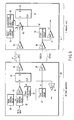
- FIG. 1 is a block diagram showing the configuration of a memory card and a host apparatus in accordance with a first embodiment of the present invention
- FIG. 2 is a diagram showing the configuration of a card interface in the host apparatus and a host interface in the memory card during a normal data transfer mode (data transfer from the host apparatus to the memory card);
- FIG. 3 is a timing chart showing data transfer based on a single data rate (SDR) scheme
- FIG. 4 is a timing chart showing data transfer based on a double data rate (DDR) scheme
- FIG. 5 is a diagram showing the configuration of the memory card and the host apparatus in accordance with the first embodiment
- FIG. 6 is a timing chart showing the case in which a delay element in accordance with the first element adjusts a clock pattern so as to shift the phase of the clock pattern from the phase of a clock signal by 180 degrees;
- FIG. 7 is a diagram showing the configuration of the card interface in the host apparatus and the host interface in the memory card during the normal data transfer mode (data transfer from the memory card to the host apparatus);
- FIG. 8 is a block diagram showing the configuration of a memory card and a host apparatus in accordance with a second embodiment of the present invention.
- FIG. 9 is a timing chart showing the case in which a delay element in accordance with the second element adjusts a clock pattern so as to shift the phase of the clock pattern from the phase of a clock signal by 180 degrees.
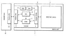
- FIG. 1 is a block diagram showing the configuration of the memory card and the host apparatus in accordance with the first embodiment of the present invention.
- the memory card 1 includes a semiconductor memory device, for example, a nonvolatile semiconductor memory device such as a NAND flash memory 3 , and a controller 4 .
- Functional blocks such as a central processing unit (CPU) 8 and read-only memory (ROM) 9 are mounted in the controller 4 .
- the NAND flash memory 3 may be a binary memory in which 1-bit information is stored in one memory cell or a multivalue memory in which information corresponding to more than 1 bit (for example, 2 bits) is stored in one memory cell.
- NOR nonvolatile semiconductor memory
- the NAND flash memory 3 and the controller 4 may be arranged on a printed circuit board (PCB) or may be formed in the same large-scale integration (LSI) circuit.
- PCB printed circuit board
- LSI large-scale integration
- the memory card 1 When connected to the host apparatus 20 , the memory card 1 is supplied with power to operate to execute a process corresponding to an access from the host apparatus 20 .
- the memory card 1 has the NAND flash memory 3 and the controller 4 as described above.
- the NAND flash memory 3 is a nonvolatile memory specified to have an erase block size (block size as an erase unit) of, for example, 256 bytes.
- the NAND flash memory 3 is also specified so that data is written to and read from the NAND flash memory 3 , for example, in 2 Kbytes.
- the NAND flash memory 3 is produced using, for example, a 0.09- ⁇ m process technique. That is, the design rule for the NAND flash memory 3 is less than 0.1 ⁇ m.
- the controller 4 includes a memory interface 5 , a host interface 6 , a buffer 7 , and random access memory (RAM) 10 .
- the memory interface 5 executes an interface process between the controller 4 and the NAND flash memory 3 .
- the host interface 6 executes an interface process between the controller 4 and the host apparatus 20 .
- a card interface 30 in the host apparatus 20 executes an interface process between the host apparatus 20 and the controller 4 .
- the card interface 30 and the host interface 6 will be shown and the data transfer between the interfaces will be described below.
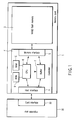
- FIG. 2 is a diagram showing the configuration of the card interface 30 in the host apparatus 20 and the host interface 6 in the memory card 1 during a normal data transfer mode (normal operation mode).
- FIG. 2 shows an example in which the host apparatus 20 transfers write data to the memory card 1 .
- FIG. 2 also shows the connection relationship under which data held in a transmission flip flop 33 is output, transferred via data I/O circuits 34 and 65 , and then held in a reception flip flop 67 .
- Clock generating circuits 32 and 70 output clock signals having a frequency that is an integer times, at least twice (in this case, twice), as large as that of a clock signal generated by the clock generating circuit 31 .
- the clock generating circuits 32 and 70 are not necessarily essential in the present embodiment but are able to realize a double data transfer rate on a bus interface with the same number of signals as shown in FIGS. 3 and 4 .
- DDR double data rate
- the clock generating circuits 32 and 70 which double the clock frequency, are used to internally control the data on the basis of one of the edges of the clock signal.
- a bus clock is generated by the clock generating circuit 31 in the host apparatus 20 and supplied to the memory card 1 via a clock I/O circuit 38 , a bus interface, and a clock I/O circuit 69 . Therefore, the write data and the clock signal are transferred in the same direction, that is, from the host apparatus 20 (card interface 30 ) to the memory card 1 (host interface 6 ).
- the host apparatus 20 receives data, the phase relationship between each data bit and the clock signal is important. Reception timings can be adjusted to some degree on the basis of the wiring length of a data line through which data is transmitted and of a clock line through which the clock signal is transmitted, or by using transistors having the same properties.
- the data I/O circuit cells 34 and 65 are bidirectional, but FIG. 2 shows only a part in which the data is transmitted from the host apparatus 20 to the memory card 1 .
- a buffer circuit 41 supplies clock signals to the other circuits in the host apparatus 20 .
- a buffer circuit 71 supplies clock signals to the other circuits in the memory card 1 .
- FIG. 2 shows a configuration established during the normal data transfer mode.
- the memory card 1 and the host apparatus 20 in accordance with the embodiment of the present invention are characterized by further having an initialization mode including a write timing adjustment mode and a read timing adjustment mode.
- the initialization mode is executed when the power is turned on or every predetermined period.
- the write timing adjustment mode is a timing adjustment mode executed by the memory card (card timing adjustment mode).
- the read timing adjustment mode is a timing adjustment mode executed by the host apparatus (host timing adjustment mode).
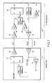
- FIG. 5 is a diagram showing the configuration of the memory card and the host apparatus in accordance with the first embodiment of the present invention. In the first embodiment, description will be given of the memory card and host apparatus having the write timing adjustment mode.
- the delay element 42 and an output selecting circuit 35 are connected to an input terminal D of the flip flop 33 in the card interface 30 in the host apparatus 20 .
- a mode selecting circuit 36 is connected to the output selecting circuit 35 .
- the mode selecting circuit 36 outputs a signal required to set the write timing adjustment mode or the normal operation mode, to the output selecting mode 35 .
- the output selecting circuit 35 Upon receiving a signal setting the write timing adjustment mode from the mode selecting circuit 36 , the output selecting circuit 35 outputs a clock signal generated by the clock generating circuit 31 to the delay element 42 . Further, upon receiving a signal setting the normal operation mode, the output selecting circuit 35 outputs write data to the delay element 42 . That is, in the write timing adjustment mode, the output selecting circuit 35 supplies the clock signal to the input terminal D of the data transmission flip flop 33 via the delay element 42 to allow a clock pattern to be output onto a data bus.
- a mode selecting circuit 61 and an adjustment value holding circuit 62 are connected to a delay element 66 in the host interface 6 in the memory card 1 .
- the delay element 66 adjusts the phase of a clock pattern input to an input section of the delay element 66 , that is, a delay value (adjustment value), so that the edge of a clock signal (a first clock signal) generated by the clock generating circuit 70 matches the edge of a clock pattern (a second clock signal) output by the data I/O circuit 65 .
- the determined adjustment value is held in the adjustment value holding circuit 62 .
- the delay element 66 Upon receiving the signal setting the normal operation mode from the mode selecting circuit 61 , the delay element 66 uses the adjustment value held in the adjustment value holding circuit 62 to adjust a delay value for write data input to the input section of the delay element 66 . That is, in the write timing adjustment mode, a clock signal supplied to a clock terminal of the reception flip flop 67 is supplied to the phase adjustable delay element 66 . On the basis of the clock signal, the delay element 66 adjusts the phase of the clock pattern to determine the current adjustment value. Moreover, the determined adjustment value is held in the adjustment value holding circuit 62 . Then, in the normal operation mode, the delay element 66 adjusts the delay value for the write data in accordance with the adjustment value held in the adjustment value holding circuit 62 . This makes it possible to ensure an appropriate setup and hold time for the reception flip flop 67 .
- the transmission flip flop 33 is supplied with a clock signal of a double frequency by the clock generating circuit 32 . Consequently, such a waveform as shown in FIG. 5 is output onto the data bus.
- the phase adjustable delay element 66 has a function of adjusting the phase of the clock pattern output onto the data bus by the host apparatus 20 and the phase of the clock signal input to the reception flip flop 67 , to particular values.
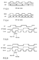
- FIG. 6 shows a timing diagram showing the case in which the delay element 66 adjusts the clock pattern so as to shift the phase of the clock pattern by 180 degrees from the phase of the clock signal (CLK ⁇ 2).
- the unadjusted clock pattern is a signal DAT and the adjusted clock pattern is a signal DAT Delayed.
- the rising edge and falling edge of the signal DAT Delayed synchronize with data change points on the data bus during the data transfer mode.
- the signal DAT Delayed is adjusted so that the rising edge of the clock signal supplied to the reception flip flop 67 corresponds to the intermediate point between the data change points.
- the delay element 66 adjusts the phase of the signal DAT Delayed so that the setup and hold time for the edge of the clock signal supplied to the reception flip flop 67 is included in the period from the rising edge to falling edge of the signal DAT Delayed (or the period from the falling edge to the rising edge). This ensures a sufficient setup and hold time for the flip flop 67 .
- write data is made of data of a plurality of bits, and the phase adjustable delay element 66 is interposed into each of a plurality of data lines through which the respective data bits is transmitted. Also in this case, individual adjustment of the delay elements enables a variation in delay among the data lines or the bits to be adjusted. This ensures a sufficient setup and hold time for the individual flip flops 67 .
- the delay values for the data in the data bus and for the clock signal in a clock bus are affected by a variation in environment such as temperature.
- a variation in environment and the like can be dealt with by periodically executing the initialization mode, including the write timing adjustment mode and the read timing adjustment mode, to readjust write and read timings.
- FIG. 7 is a diagram showing the configuration of the card interface 30 in the host apparatus 20 and the host interface 6 in the memory card 1 during the normal data transfer mode.
- FIG. 7 shows an example in which the memory card 1 transfers read data to the host apparatus 20 .
- FIG. 7 also shows the connection relationship under which data output by a transmission flip flop 22 is transferred via the data I/O circuits 65 and 34 and then loaded into a reception flip flop 24 .
- FIG. 7 shows the memory card (host interface 6 ) 1 on the left and the host apparatus (card interface 30 ) 20 on the right.
- a clock signal generated by the clock generating circuit 31 in the card interface 30 in the host apparatus 20 is supplied to the host interface 6 in the memory card 1 via clock I/O circuits 38 and 69 .
- the clock signal supplied by the host interface 6 has its frequency doubled by the clock generating circuit 21 .
- the resulting clock signal is supplied to a clock terminal of the transmission flip flop 22 .
- the transmission flip flop 22 holds read data input to the input terminal D in the DDR mode and outputs the data from an output terminal Q to the data bus. As seen in FIG. 7 , the read data and the clock signal are transmitted in the opposite directions.
- the data I/O circuit cells 34 and 65 are bidirectional, but FIG. 7 shows only a part in which the data is transmitted from the memory card 1 to the host apparatus 20 .
- the read data output via the data I/O circuit 65 by the transmission flip flop 22 is supplied to the delay element 23 via the data bus and the data I/O circuit 34 in the host apparatus 20 .
- the delay element 23 eliminates a variation among the data bits of the read data supplied to the delay element 23 , which is able to adjust the delay value.
- the resulting read data is supplied to and held in the reception flip flop 24 . If a clock signal generated by the host apparatus 20 is input to the input terminal D of the flip flop terminal 22 and a clock pattern then output to the host apparatus 20 is used to adjust read timings, then the read data passes through the transmission flip flop 22 in the memory card 1 back to the reception flip flop 24 in the host apparatus 20 using the clock signal generated by the host apparatus 20 as a start point.
- the delay in the path varies very significantly.
- the controller and the memory circuit are arranged onboard, and the wiring between the controller and the memory circuit can be fixed.
- the length of an SD bus line and the properties of the element vary depending on the implementations of the host system and the card. This prevents the delay value from being pre-calculated.
- a phase adjustable delay element 25 needs to be interposed in front of the clock generating circuit 26 , which doubles the frequency of the clock signal, to adjust the delay value (phase) of the clock signal supplied to the flip flop 24 .
- FIG. 8 is a block diagram showing the configuration of the memory card and the host apparatus in accordance with the second embodiment of the present invention. In the second embodiment, description will be given of the memory card and host apparatus having the read timing adjustment mode.
- the delay element 27 and the output selecting circuit 35 are connected to the input terminal D of the flip flop 22 in the host interface 6 in the memory card 1 .
- the mode selecting circuit 36 is connected to the output selecting circuit 35 .
- the mode selecting circuit 36 outputs a signal required to set the read timing adjustment mode or the normal operation mode, to the output selecting mode 35 .
- the output selecting circuit 35 Upon receiving a signal setting the read timing adjustment mode from the mode selecting circuit 36 , the output selecting circuit 35 outputs a clock signal generated by the clock generating circuit 31 and supplied to clock I/O circuit 69 to the delay element 27 . Further, upon receiving a signal setting the normal operation mode, the output selecting circuit 35 outputs read data to the delay element 27 . That is, in the read timing adjustment mode, the output selecting circuit 35 supplies the clock signal to the input terminal D of the transmission flip flop 22 via the delay element 27 to allow a clock pattern to be output onto a data bus.
- a phase detecting circuit 28 determining the delay value is connected to the delay element 23 interposed in the data bus in the card interface 30 in the host apparatus 20 .
- the mode selecting circuit 61 and the adjustment value holding circuit 62 are connected to the delay element 25 . Further, an output from the delay element 23 is supplied to the delay element 25 .
- the delay element 25 adjusts the phase of a clock signal input to an input section of the delay element 25 , that is, a delay value (adjustment value), so that the edge of a clock signal (a first clock signal) generated by the clock generating circuit 31 matches the edge of a clock pattern (a second clock signal) output by the delay element 23 .
- the determined adjustment value is held in the adjustment value holding circuit 62 .
- the delay element 25 uses the adjustment value held in the adjustment value holding circuit 62 to adjust a delay value for the clock signal input to the input section of the delay element 25 . That is, in the read timing adjustment mode, the clock pattern output by the delay element 23 is supplied to the phase adjustable delay element 25 in order to adjust the setup and hold time for the reception flip flop 24 . On the basis of the clock pattern, the delay element 25 adjusts the phase of the clock signal to determine the current adjustment value. Moreover, the determined adjustment value is held in the adjustment value holding circuit 62 . Then, in the normal operation mode, the delay element 25 adjusts the delay value for the clock signal in accordance with the adjustment value held in the adjustment value holding circuit 62 . This makes it possible to ensure the appropriate setup and hold time for the reception flip flop 24 .
- the transmission flip flop 22 is supplied with a clock signal of a double frequency. Consequently, such a waveform as shown in FIG. 8 is output onto the data bus.
- the phase detecting circuit 28 has a function of detecting a phase difference among a plurality of data bits and adjusting the delay element 23 so that the delay values for all the data bits other than the latest one are set on the basis of the delay value for the latest data bit to inhibit a variation in delay among the data bits.
- the phase adjustable delay element 25 has a function of adjusting the phase of the clock pattern output onto the data bus by the memory card 1 and the phase of the clock signal input to the reception flip flop 24 , to particular values.
- FIG. 9 is a timing chart showing the case in which the delay element 25 adjusts the clock pattern so as to shift the phase of the clock signal from the phase of the clock pattern by 180 degrees.
- the signal DAT Delayed shows an adjusted waveform.
- the rising edge and falling edge of the signal DAT Delayed synchronize with the rising edge and falling edge of the clock pattern DAT on the data bus and indicate data change points on the data bus.
- the rising edge of the clock signal (CLK ⁇ 2) supplied to the flip flop 24 is adjusted to the intermediate point between the data change points. This ensures a sufficient setup and hold time for the flip flop 24 .
- the results are held in the adjustment value holding circuit 62 . Further, if the delay may be varied by, for example, a variation in temperature, the adjustment value (delay value) can be readjusted by executing the adjustment mode again periodically or under particular conditions.
- the embodiment of the present invention can provide the memory card and host apparatus which are able to stably transfer data even when operating at a high clock frequency.
- each of the above embodiments can not only be individually carried out not but also be appropriately combined.
- each of the above embodiments includes various levels of inventions. The various levels of inventions can thus be extracted by appropriately combining a plurality of the components disclosed in the embodiments.
Abstract
A memory card includes a clock I/O circuit, a data I/O circuit, a delay element, and an adjustment value holding circuit. The clock input/output circuit receives a first clock from a host apparatus. The data I/O circuit receives a second clock from the host apparatus in a write timing adjustment mode. The data I/O circuit transmits and receives data to and from the host apparatus in a data transfer mode. In the write timing adjustment mode, the delay element adjusts a phase of the second clock in accordance with the first clock so as to receive the data received in the data transfer mode in response to the first clock. The adjustment value holding circuit holds an adjustment value for the phase of the second clock adjusted. In the data transfer mode, the delay element adjusts a phase of the data in accordance with the adjustment value.
Description
- This application is based upon and claims the benefit of priority from prior Japanese Patent Application No. 2006-269967, filed Sep. 29, 2006, the entire contents of which are incorporated herein by reference.
- 1. Field of the Invention
- The present invention relates to a memory card having a memory device on which a data write operation, a data read operation, and a data erase operation are performed in response to an access from a host apparatus, and also relates to the host apparatus. For example, the present invention relates to timing adjustment for a bus interface that connects the memory card and the host apparatus together.
- 2. Description of the Related Art
- Memory cards such as SD memory cards, which are one type of removable memory devices, have often been used in various portable electronic apparatuses such as personal computers, PDAs, cameras, and cellular phones (see, for example, Jpn. Pat. Appln. KOKAI Publication No. 2003-196613). The SD memory card is able to transfer data at a maximum of 25 MB/sec owing to an expanded high speed mode. However, next-generation memory cards are desired to have a transfer ability equivalent to at least 50 MB/sec.
- However, with bus interfaces used in memory cards and based on the current scheme, it is difficult to control operation timings owing to a variation in delay. This in turn makes it difficult to increase the frequency of clock signals used to synchronize operations. The timing and element properties depend on the implementations and combination of the memory card and a host system. This makes it impossible to pre-calculate a predetermined delay value. In this respect, the memory card is different from onboard DRAMs (Dynamic Random Access Memories) and the like.
- A first aspect of the present invention provides a memory card accessed by a host apparatus, the memory card comprising a clock input/output circuit which receives a first clock signal from the host apparatus via a clock line; a data I/O circuit which receives a second clock signal from the host apparatus via a data line in a write timing adjustment mode executed by the memory card, the data I/O circuit transmitting and receiving data to and from the host apparatus via the data line in a data transfer mode; a delay element which, in the write timing adjustment mode, adjusts a phase of the second clock signal output by the data I/O circuit in accordance with the first clock signal so as to receive the data received in the data transfer mode in response to the first clock signal supplied by the clock input/output circuit; and an adjustment value holding circuit which holds an adjustment value for the phase of the second clock signal adjusted by the delay element. In the data transfer mode, the delay element adjusts a phase of the data output by the data I/O circuit in accordance with the adjustment value held in the adjustment value holding circuit.
- A second aspect of the present invention provides a host apparatus accessing a memory card, the host apparatus comprising a clock generating circuit which generates a first clock; a clock input/output circuit which supplies the first clock signal to the memory card via a clock line; a data I/O circuit which receives a second clock signal generated on the basis of the first clock signal, from the memory card via a data line in a read timing adjustment mode executed by the host apparatus, the data I/O circuit transmitting and receiving data to and from the memory card via the data line in a data transfer mode; a first delay element which, in the read timing adjustment mode, adjusts a phase of the first clock signal in accordance with the second clock signal output by the data I/O circuit; and an adjustment value holding circuit which holds an adjustment value for a phase of the first clock signal adjusted by the first delay element. In the data transfer mode, the first delay element adjusts the phase of the first clock generated by the clock generating circuit in accordance with the adjustment value held in the adjustment value holding circuit.
-
FIG. 1 is a block diagram showing the configuration of a memory card and a host apparatus in accordance with a first embodiment of the present invention; -
FIG. 2 is a diagram showing the configuration of a card interface in the host apparatus and a host interface in the memory card during a normal data transfer mode (data transfer from the host apparatus to the memory card); -
FIG. 3 is a timing chart showing data transfer based on a single data rate (SDR) scheme; -
FIG. 4 is a timing chart showing data transfer based on a double data rate (DDR) scheme; -
FIG. 5 is a diagram showing the configuration of the memory card and the host apparatus in accordance with the first embodiment; -
FIG. 6 is a timing chart showing the case in which a delay element in accordance with the first element adjusts a clock pattern so as to shift the phase of the clock pattern from the phase of a clock signal by 180 degrees; -
FIG. 7 is a diagram showing the configuration of the card interface in the host apparatus and the host interface in the memory card during the normal data transfer mode (data transfer from the memory card to the host apparatus); -
FIG. 8 is a block diagram showing the configuration of a memory card and a host apparatus in accordance with a second embodiment of the present invention; and -
FIG. 9 is a timing chart showing the case in which a delay element in accordance with the second element adjusts a clock pattern so as to shift the phase of the clock pattern from the phase of a clock signal by 180 degrees. - Embodiments of the present invention will be described below with reference to the drawings. In the description below, the same parts are denoted by the same reference numbers throughout the drawings.
- First, description will be given of a memory card and a host apparatus in accordance with a first embodiment of the present invention.
-
FIG. 1 is a block diagram showing the configuration of the memory card and the host apparatus in accordance with the first embodiment of the present invention. - As shown in
FIG. 1 , thememory card 1 includes a semiconductor memory device, for example, a nonvolatile semiconductor memory device such as aNAND flash memory 3, and acontroller 4. Functional blocks such as a central processing unit (CPU) 8 and read-only memory (ROM) 9 are mounted in thecontroller 4. TheNAND flash memory 3 may be a binary memory in which 1-bit information is stored in one memory cell or a multivalue memory in which information corresponding to more than 1 bit (for example, 2 bits) is stored in one memory cell. Here, an example in which a NAND flash memory is used will be described. However, the present invention is not limited to this but is applicable to other nonvolatile semiconductor memories such as NOR memories. - Further, although not shown, the
NAND flash memory 3 and thecontroller 4 may be arranged on a printed circuit board (PCB) or may be formed in the same large-scale integration (LSI) circuit. - When connected to the
host apparatus 20, thememory card 1 is supplied with power to operate to execute a process corresponding to an access from thehost apparatus 20. Thememory card 1 has theNAND flash memory 3 and thecontroller 4 as described above. - The
NAND flash memory 3 is a nonvolatile memory specified to have an erase block size (block size as an erase unit) of, for example, 256 bytes. TheNAND flash memory 3 is also specified so that data is written to and read from theNAND flash memory 3, for example, in 2 Kbytes. TheNAND flash memory 3 is produced using, for example, a 0.09-μm process technique. That is, the design rule for theNAND flash memory 3 is less than 0.1 μm. - In addition to
CPU 8 and ROM 9, described above, thecontroller 4 includes amemory interface 5, ahost interface 6, abuffer 7, and random access memory (RAM) 10. Thememory interface 5 executes an interface process between thecontroller 4 and theNAND flash memory 3. Thehost interface 6 executes an interface process between thecontroller 4 and thehost apparatus 20. Acard interface 30 in thehost apparatus 20 executes an interface process between thehost apparatus 20 and thecontroller 4. - The
card interface 30 and thehost interface 6 will be shown and the data transfer between the interfaces will be described below. -
FIG. 2 is a diagram showing the configuration of thecard interface 30 in thehost apparatus 20 and thehost interface 6 in thememory card 1 during a normal data transfer mode (normal operation mode).FIG. 2 shows an example in which thehost apparatus 20 transfers write data to thememory card 1.FIG. 2 also shows the connection relationship under which data held in atransmission flip flop 33 is output, transferred via data I/O circuits reception flip flop 67. -
Clock generating circuits clock generating circuit 31. Theclock generating circuits FIGS. 3 and 4 . With a double data rate (DDR) scheme, data DAT is transferred in half the period of a bus clock SDCLK. Theclock generating circuits - With an SD memory card, a bus clock is generated by the
clock generating circuit 31 in thehost apparatus 20 and supplied to thememory card 1 via a clock I/O circuit 38, a bus interface, and a clock I/O circuit 69. Therefore, the write data and the clock signal are transferred in the same direction, that is, from the host apparatus 20 (card interface 30) to the memory card 1 (host interface 6). When thehost apparatus 20 receives data, the phase relationship between each data bit and the clock signal is important. Reception timings can be adjusted to some degree on the basis of the wiring length of a data line through which data is transmitted and of a clock line through which the clock signal is transmitted, or by using transistors having the same properties. However, since the connection between thememory card 1 and thehost apparatus 20 cannot be identified, the reception timing depends on the implementation. It is thus expected that the delay varies among the data bits. The data I/O circuit cells FIG. 2 shows only a part in which the data is transmitted from thehost apparatus 20 to thememory card 1. Abuffer circuit 41 supplies clock signals to the other circuits in thehost apparatus 20. Abuffer circuit 71 supplies clock signals to the other circuits in thememory card 1. -
FIG. 2 , described above, shows a configuration established during the normal data transfer mode. However, thememory card 1 and thehost apparatus 20 in accordance with the embodiment of the present invention are characterized by further having an initialization mode including a write timing adjustment mode and a read timing adjustment mode. The initialization mode is executed when the power is turned on or every predetermined period. The write timing adjustment mode is a timing adjustment mode executed by the memory card (card timing adjustment mode). The read timing adjustment mode is a timing adjustment mode executed by the host apparatus (host timing adjustment mode). -
FIG. 5 is a diagram showing the configuration of the memory card and the host apparatus in accordance with the first embodiment of the present invention. In the first embodiment, description will be given of the memory card and host apparatus having the write timing adjustment mode. - Differences from the configuration shown in
FIG. 2 will be shown below. Thedelay element 42 and anoutput selecting circuit 35 are connected to an input terminal D of theflip flop 33 in thecard interface 30 in thehost apparatus 20. Amode selecting circuit 36 is connected to theoutput selecting circuit 35. Themode selecting circuit 36 outputs a signal required to set the write timing adjustment mode or the normal operation mode, to theoutput selecting mode 35. Upon receiving a signal setting the write timing adjustment mode from themode selecting circuit 36, theoutput selecting circuit 35 outputs a clock signal generated by theclock generating circuit 31 to thedelay element 42. Further, upon receiving a signal setting the normal operation mode, theoutput selecting circuit 35 outputs write data to thedelay element 42. That is, in the write timing adjustment mode, theoutput selecting circuit 35 supplies the clock signal to the input terminal D of the datatransmission flip flop 33 via thedelay element 42 to allow a clock pattern to be output onto a data bus. - Moreover, a
mode selecting circuit 61 and an adjustmentvalue holding circuit 62 are connected to adelay element 66 in thehost interface 6 in thememory card 1. Upon receiving the signal setting the write timing adjustment mode from themode selecting circuit 61, thedelay element 66 adjusts the phase of a clock pattern input to an input section of thedelay element 66, that is, a delay value (adjustment value), so that the edge of a clock signal (a first clock signal) generated by theclock generating circuit 70 matches the edge of a clock pattern (a second clock signal) output by the data I/O circuit 65. At this time, the determined adjustment value is held in the adjustmentvalue holding circuit 62. Upon receiving the signal setting the normal operation mode from themode selecting circuit 61, thedelay element 66 uses the adjustment value held in the adjustmentvalue holding circuit 62 to adjust a delay value for write data input to the input section of thedelay element 66. That is, in the write timing adjustment mode, a clock signal supplied to a clock terminal of thereception flip flop 67 is supplied to the phaseadjustable delay element 66. On the basis of the clock signal, thedelay element 66 adjusts the phase of the clock pattern to determine the current adjustment value. Moreover, the determined adjustment value is held in the adjustmentvalue holding circuit 62. Then, in the normal operation mode, thedelay element 66 adjusts the delay value for the write data in accordance with the adjustment value held in the adjustmentvalue holding circuit 62. This makes it possible to ensure an appropriate setup and hold time for thereception flip flop 67. - In the write timing adjustment mode, the
transmission flip flop 33 is supplied with a clock signal of a double frequency by theclock generating circuit 32. Consequently, such a waveform as shown inFIG. 5 is output onto the data bus. The phaseadjustable delay element 66 has a function of adjusting the phase of the clock pattern output onto the data bus by thehost apparatus 20 and the phase of the clock signal input to thereception flip flop 67, to particular values. -
FIG. 6 shows a timing diagram showing the case in which thedelay element 66 adjusts the clock pattern so as to shift the phase of the clock pattern by 180 degrees from the phase of the clock signal (CLK×2). The unadjusted clock pattern is a signal DAT and the adjusted clock pattern is a signal DAT Delayed. With the DDR scheme, the rising edge and falling edge of the signal DAT Delayed synchronize with data change points on the data bus during the data transfer mode. Thus, the signal DAT Delayed is adjusted so that the rising edge of the clock signal supplied to thereception flip flop 67 corresponds to the intermediate point between the data change points. In other words, thedelay element 66 adjusts the phase of the signal DAT Delayed so that the setup and hold time for the edge of the clock signal supplied to thereception flip flop 67 is included in the period from the rising edge to falling edge of the signal DAT Delayed (or the period from the falling edge to the rising edge). This ensures a sufficient setup and hold time for theflip flop 67. Further, write data is made of data of a plurality of bits, and the phaseadjustable delay element 66 is interposed into each of a plurality of data lines through which the respective data bits is transmitted. Also in this case, individual adjustment of the delay elements enables a variation in delay among the data lines or the bits to be adjusted. This ensures a sufficient setup and hold time for the individual flip flops 67. The delay values for the data in the data bus and for the clock signal in a clock bus are affected by a variation in environment such as temperature. Thus, a variation in environment and the like can be dealt with by periodically executing the initialization mode, including the write timing adjustment mode and the read timing adjustment mode, to readjust write and read timings. - Now, description will be given of a memory card and a host apparatus in accordance with a second embodiment. Arrangements similar to those in the first embodiment are denoted by the same reference numbers and will not be described below. The configuration of the memory card and host apparatus shown in
FIG. 1 is similarly applicable to the second embodiment. -
FIG. 7 is a diagram showing the configuration of thecard interface 30 in thehost apparatus 20 and thehost interface 6 in thememory card 1 during the normal data transfer mode.FIG. 7 shows an example in which thememory card 1 transfers read data to thehost apparatus 20.FIG. 7 also shows the connection relationship under which data output by atransmission flip flop 22 is transferred via the data I/O circuits reception flip flop 24. UnlikeFIGS. 2 and 5 ,FIG. 7 shows the memory card (host interface 6) 1 on the left and the host apparatus (card interface 30) 20 on the right. - A clock signal generated by the
clock generating circuit 31 in thecard interface 30 in thehost apparatus 20 is supplied to thehost interface 6 in thememory card 1 via clock I/O circuits host interface 6 has its frequency doubled by theclock generating circuit 21. The resulting clock signal is supplied to a clock terminal of thetransmission flip flop 22. Thetransmission flip flop 22 holds read data input to the input terminal D in the DDR mode and outputs the data from an output terminal Q to the data bus. As seen inFIG. 7 , the read data and the clock signal are transmitted in the opposite directions. The data I/O circuit cells FIG. 7 shows only a part in which the data is transmitted from thememory card 1 to thehost apparatus 20. - The read data output via the data I/
O circuit 65 by thetransmission flip flop 22 is supplied to thedelay element 23 via the data bus and the data I/O circuit 34 in thehost apparatus 20. Thedelay element 23 eliminates a variation among the data bits of the read data supplied to thedelay element 23, which is able to adjust the delay value. The resulting read data is supplied to and held in thereception flip flop 24. If a clock signal generated by thehost apparatus 20 is input to the input terminal D of theflip flop terminal 22 and a clock pattern then output to thehost apparatus 20 is used to adjust read timings, then the read data passes through thetransmission flip flop 22 in thememory card 1 back to thereception flip flop 24 in thehost apparatus 20 using the clock signal generated by thehost apparatus 20 as a start point. Owing to the large length of the path, the delay in the path varies very significantly. When DRAM or the like using DDR is used, the controller and the memory circuit are arranged onboard, and the wiring between the controller and the memory circuit can be fixed. However, for the SD memory card, the length of an SD bus line and the properties of the element vary depending on the implementations of the host system and the card. This prevents the delay value from being pre-calculated. To correctly receive data, it is necessary to adjust the phase of the clock signal supplied to theflip flop 24 and the phase of the input data so as to provide the appropriate setup and hold time for theflip flop 24. Thus, a phaseadjustable delay element 25 needs to be interposed in front of theclock generating circuit 26, which doubles the frequency of the clock signal, to adjust the delay value (phase) of the clock signal supplied to theflip flop 24. -
FIG. 8 is a block diagram showing the configuration of the memory card and the host apparatus in accordance with the second embodiment of the present invention. In the second embodiment, description will be given of the memory card and host apparatus having the read timing adjustment mode. - Differences from the configuration shown in
FIG. 7 will be shown below. Thedelay element 27 and theoutput selecting circuit 35 are connected to the input terminal D of theflip flop 22 in thehost interface 6 in thememory card 1. Themode selecting circuit 36 is connected to theoutput selecting circuit 35. Themode selecting circuit 36 outputs a signal required to set the read timing adjustment mode or the normal operation mode, to theoutput selecting mode 35. Upon receiving a signal setting the read timing adjustment mode from themode selecting circuit 36, theoutput selecting circuit 35 outputs a clock signal generated by theclock generating circuit 31 and supplied to clock I/O circuit 69 to thedelay element 27. Further, upon receiving a signal setting the normal operation mode, theoutput selecting circuit 35 outputs read data to thedelay element 27. That is, in the read timing adjustment mode, theoutput selecting circuit 35 supplies the clock signal to the input terminal D of thetransmission flip flop 22 via thedelay element 27 to allow a clock pattern to be output onto a data bus. - Moreover, a
phase detecting circuit 28 determining the delay value is connected to thedelay element 23 interposed in the data bus in thecard interface 30 in thehost apparatus 20. Themode selecting circuit 61 and the adjustmentvalue holding circuit 62 are connected to thedelay element 25. Further, an output from thedelay element 23 is supplied to thedelay element 25. Upon receiving the signal setting the read timing adjustment mode from themode selecting circuit 61, thedelay element 25 adjusts the phase of a clock signal input to an input section of thedelay element 25, that is, a delay value (adjustment value), so that the edge of a clock signal (a first clock signal) generated by theclock generating circuit 31 matches the edge of a clock pattern (a second clock signal) output by thedelay element 23. At this time, the determined adjustment value is held in the adjustmentvalue holding circuit 62. Upon receiving the signal setting the normal operation mode from themode selecting circuit 61, thedelay element 25 uses the adjustment value held in the adjustmentvalue holding circuit 62 to adjust a delay value for the clock signal input to the input section of thedelay element 25. That is, in the read timing adjustment mode, the clock pattern output by thedelay element 23 is supplied to the phaseadjustable delay element 25 in order to adjust the setup and hold time for thereception flip flop 24. On the basis of the clock pattern, thedelay element 25 adjusts the phase of the clock signal to determine the current adjustment value. Moreover, the determined adjustment value is held in the adjustmentvalue holding circuit 62. Then, in the normal operation mode, thedelay element 25 adjusts the delay value for the clock signal in accordance with the adjustment value held in the adjustmentvalue holding circuit 62. This makes it possible to ensure the appropriate setup and hold time for thereception flip flop 24. - In the read timing adjustment mode, the
transmission flip flop 22 is supplied with a clock signal of a double frequency. Consequently, such a waveform as shown inFIG. 8 is output onto the data bus. Thephase detecting circuit 28 has a function of detecting a phase difference among a plurality of data bits and adjusting thedelay element 23 so that the delay values for all the data bits other than the latest one are set on the basis of the delay value for the latest data bit to inhibit a variation in delay among the data bits. The phaseadjustable delay element 25 has a function of adjusting the phase of the clock pattern output onto the data bus by thememory card 1 and the phase of the clock signal input to thereception flip flop 24, to particular values. -
FIG. 9 is a timing chart showing the case in which thedelay element 25 adjusts the clock pattern so as to shift the phase of the clock signal from the phase of the clock pattern by 180 degrees. The signal DAT Delayed shows an adjusted waveform. The rising edge and falling edge of the signal DAT Delayed synchronize with the rising edge and falling edge of the clock pattern DAT on the data bus and indicate data change points on the data bus. The rising edge of the clock signal (CLK×2) supplied to theflip flop 24 is adjusted to the intermediate point between the data change points. This ensures a sufficient setup and hold time for theflip flop 24. - Once the write timing adjustment mode and read timing adjustment mode in accordance with the first and second embodiments are executed, the results are held in the adjustment
value holding circuit 62. Further, if the delay may be varied by, for example, a variation in temperature, the adjustment value (delay value) can be readjusted by executing the adjustment mode again periodically or under particular conditions. - The embodiment of the present invention can provide the memory card and host apparatus which are able to stably transfer data even when operating at a high clock frequency.
- Further, the above embodiments can not only be individually carried out not but also be appropriately combined. Moreover, each of the above embodiments includes various levels of inventions. The various levels of inventions can thus be extracted by appropriately combining a plurality of the components disclosed in the embodiments.
- Additional advantages and modifications will readily occur to those skilled in the art. Therefore, the invention in its broader aspects is not limited to the specific details and representative embodiments shown and described herein. Accordingly, various modifications may be made without departing from the spirit or scope of the general inventive concept as defined by the appended claims and their equivalents.
Claims (13)
1. A memory card accessed by a host apparatus, the memory card comprising:
a clock input/output circuit which receives a first clock signal from the host apparatus via a clock line;
a data I/O circuit which receives a second clock signal from the host apparatus via a data line in a write timing adjustment mode executed by the memory card, the data I/O circuit transmitting and receiving data to and from the host apparatus via the data line in a data transfer mode;
a delay element which, in the write timing adjustment mode, adjusts a phase of the second clock signal output by the data I/O circuit in accordance with the first clock signal so as to receive the data received in the data transfer mode in response to the first clock signal supplied by the clock input/output circuit; and
an adjustment value holding circuit which holds an adjustment value for the phase of the second clock signal adjusted by the delay element,
wherein in the data transfer mode, the delay element adjusts a phase of the data output by the data I/O circuit in accordance with the adjustment value held in the adjustment value holding circuit.
2. The memory card according to claim 1 , further comprising a flip flop which, in the data transfer mode, holds the data having the phase adjusted by the delay element, in synchronism with the first clock signal.
3. The memory card according to claim 1 , wherein the delay element adjusts the phase of the second clock signal so that a setup time and a hold time for an edge of the first clock signal are included in a period from a rising edge to a falling edge of the second clock signal.
4. The memory card according to claim 1 , further comprising a clock generating circuit which generates a third clock signal having a frequency which is integer times as large as that of the first clock signal; and
a flip flop which holds the data having the phase adjusted by the delay element, in synchronism with the third clock signal.
5. The memory card according to claim 1 , further comprising a mode selecting circuit which sets one of the data transfer mode and the write timing adjustment mode for the delay element.
6. The memory card according to claim 2 , further comprising a nonvolatile semiconductor memory device which stores data output by the flip flop.
7. The memory card according to claim 6 , wherein the nonvolatile semiconductor memory device includes a NAND flash memory.
8. A host apparatus accessing a memory card, the host apparatus comprising:
a clock generating circuit which generates a first clock;
a clock input/output circuit which supplies the first clock signal to the memory card via a clock line;
a data I/O circuit which receives a second clock signal generated on the basis of the first clock signal, from the memory card via a data line in a read timing adjustment mode executed by the host apparatus, the data I/O circuit transmitting and receiving data to and from the memory card via the data line in a data transfer mode;
a first delay element which, in the read timing adjustment mode, adjusts a phase of the first clock signal in accordance with the second clock signal output by the data I/O circuit; and
an adjustment value holding circuit which holds an adjustment value for a phase of the first clock signal adjusted by the first delay element,
wherein in the data transfer mode, the first delay element adjusts the phase of the first clock generated by the clock generating circuit in accordance with the adjustment value held in the adjustment value holding circuit.
9. The host apparatus according to claim 8 , further comprising a flip flop which, in the data transfer mode, holds the data output by the data I/O circuit, in synchronism with the first clock signal adjusted by the first delay element.
10. The host apparatus according to claim 8 , wherein the first delay element adjusts the phase of the first clock signal so that a setup time and a hold time for an edge of the first clock signal are included in a period from a rising edge to a falling edge of the second clock signal.
11. The host apparatus according to claim 8 , further comprising a phase detecting circuit which detects a phase difference in the second clock signal output by the data I/O circuit; and
a second delay element which adjusts the phase of the second clock signal in accordance with the phase difference detected by the phase detecting circuit.
12. The host apparatus according to claim 8 , further comprising a clock generating circuit which generates a third clock signal having a frequency which is integer times as large as that of the first clock signal having the phase adjusted by the first delay element; and
a flip flop which holds the data output by the data I/O circuit, in synchronism with the third clock signal.
13. The host apparatus according to claim 8 , further comprising a mode selecting circuit which sets one of the data transfer mode and the write timing adjustment mode for the first delay element.
Priority Applications (1)
| Application Number | Priority Date | Filing Date | Title |
|---|---|---|---|
| US12/904,771 US20110035615A1 (en) | 2006-09-29 | 2010-10-14 | Memory card having memory device and host apparatus accessing memory card |
Applications Claiming Priority (2)
| Application Number | Priority Date | Filing Date | Title |
|---|---|---|---|
| JP2006-269967 | 2006-09-29 | ||
| JP2006269967A JP4823009B2 (en) | 2006-09-29 | 2006-09-29 | Memory card and host device |
Related Child Applications (1)
| Application Number | Title | Priority Date | Filing Date |
|---|---|---|---|
| US12/904,771 Continuation US20110035615A1 (en) | 2006-09-29 | 2010-10-14 | Memory card having memory device and host apparatus accessing memory card |
Publications (2)
| Publication Number | Publication Date |
|---|---|
| US20080098142A1 true US20080098142A1 (en) | 2008-04-24 |
| US7827431B2 US7827431B2 (en) | 2010-11-02 |
Family
ID=39319396
Family Applications (2)
| Application Number | Title | Priority Date | Filing Date |
|---|---|---|---|
| US11/862,741 Expired - Fee Related US7827431B2 (en) | 2006-09-29 | 2007-09-27 | Memory card having memory device and host apparatus accessing memory card |
| US12/904,771 Abandoned US20110035615A1 (en) | 2006-09-29 | 2010-10-14 | Memory card having memory device and host apparatus accessing memory card |
Family Applications After (1)
| Application Number | Title | Priority Date | Filing Date |
|---|---|---|---|
| US12/904,771 Abandoned US20110035615A1 (en) | 2006-09-29 | 2010-10-14 | Memory card having memory device and host apparatus accessing memory card |
Country Status (2)
| Country | Link |
|---|---|
| US (2) | US7827431B2 (en) |
| JP (1) | JP4823009B2 (en) |
Cited By (6)
| Publication number | Priority date | Publication date | Assignee | Title |
|---|---|---|---|---|
| US20080256282A1 (en) * | 2007-04-16 | 2008-10-16 | Zhendong Guo | Calibration of Read/Write Memory Access via Advanced Memory Buffer |
| US20100077134A1 (en) * | 2008-09-23 | 2010-03-25 | Mediatek Inc. | Flash device and method for improving performance of flash device |
| CN102385912A (en) * | 2010-08-31 | 2012-03-21 | 株式会社东芝 | Host controller for setting sampling phase, semiconductor device and method |
| US8286024B2 (en) | 2008-12-26 | 2012-10-09 | Kabushiki Kaisha Toshiba | Memory device, host device, and sampling clock adjusting method |
| WO2014055794A1 (en) * | 2012-10-05 | 2014-04-10 | Qualcomm Incorporated | Algorithm for optimal usage of external memory tuning sequence |
| US20200192570A1 (en) * | 2018-12-13 | 2020-06-18 | Micron Technology, Inc. | Host clock bit slip calibration |
Families Citing this family (7)
| Publication number | Priority date | Publication date | Assignee | Title |
|---|---|---|---|---|
| JP4823009B2 (en) * | 2006-09-29 | 2011-11-24 | 株式会社東芝 | Memory card and host device |
| JP2010219751A (en) | 2009-03-16 | 2010-09-30 | Elpida Memory Inc | Semiconductor device |
| JP5259563B2 (en) * | 2009-12-22 | 2013-08-07 | 株式会社東芝 | Information processing apparatus and control method thereof |
| JP5330340B2 (en) | 2010-08-31 | 2013-10-30 | 株式会社東芝 | Host controller and method for correcting sampling phase |
| JP5801158B2 (en) * | 2011-10-21 | 2015-10-28 | ラピスセミコンダクタ株式会社 | RAM storage device |
| US9772651B2 (en) | 2012-09-14 | 2017-09-26 | Samsung Electronics Co., Ltd. | Embedded multimedia card (eMMC), host controlling eMMC, and method operating eMMC system including the use of a switch command defining an adjustment delay for a data signal |
| KR102193468B1 (en) | 2014-04-04 | 2020-12-21 | 삼성전자주식회사 | Memory device of adaptively calibrating timing margin and integrated circuit including the same |
Citations (7)
| Publication number | Priority date | Publication date | Assignee | Title |
|---|---|---|---|---|
| US5386539A (en) * | 1990-09-28 | 1995-01-31 | Fuji Photo Film Co., Ltd. | IC memory card comprising an EEPROM with data and address buffering for controlling the writing/reading of data to EEPROM |
| US5915105A (en) * | 1990-04-18 | 1999-06-22 | Rambus Inc. | Integrated circuit I/O using a high performance bus interface |
| US20030075609A1 (en) * | 2001-10-19 | 2003-04-24 | Samsung Electronics Co., Ltd. | Memory card, digital device, and method of data interfacing between memory card and digital device |
| US20040153582A1 (en) * | 2002-12-13 | 2004-08-05 | Renesas Technology Corp. | Data processor and memory card |
| US6943595B2 (en) * | 2002-09-27 | 2005-09-13 | Matsushita Electric Industrial Co., Ltd | Synchronization circuit |
| US20080034142A1 (en) * | 2006-08-07 | 2008-02-07 | Nam-Phil Jo | Data transfer in memory card system |
| US20080046775A1 (en) * | 2006-08-21 | 2008-02-21 | Realtek Semiconductor Corp. | Memory card control chip |
Family Cites Families (7)
| Publication number | Priority date | Publication date | Assignee | Title |
|---|---|---|---|---|
| JP3125348B2 (en) * | 1991-09-11 | 2001-01-15 | 日本電気株式会社 | Parallel bit synchronization method |
| JPH0798617A (en) * | 1993-05-20 | 1995-04-11 | Hitachi Ltd | Clock generation circuit and bus system |
| JP3489147B2 (en) * | 1993-09-20 | 2004-01-19 | 株式会社日立製作所 | Data transfer method |
| JP4090088B2 (en) * | 1996-09-17 | 2008-05-28 | 富士通株式会社 | Semiconductor device system and semiconductor device |
| JP3641239B2 (en) | 2001-12-27 | 2005-04-20 | 株式会社東芝 | Apparatus and method for controlling a memory card |
| JP4823009B2 (en) * | 2006-09-29 | 2011-11-24 | 株式会社東芝 | Memory card and host device |
| JP5341503B2 (en) * | 2008-12-26 | 2013-11-13 | 株式会社東芝 | Memory device, host device, and sampling clock adjustment method |
-
2006
- 2006-09-29 JP JP2006269967A patent/JP4823009B2/en not_active Expired - Fee Related
-
2007
- 2007-09-27 US US11/862,741 patent/US7827431B2/en not_active Expired - Fee Related
-
2010
- 2010-10-14 US US12/904,771 patent/US20110035615A1/en not_active Abandoned
Patent Citations (9)
| Publication number | Priority date | Publication date | Assignee | Title |
|---|---|---|---|---|
| US5915105A (en) * | 1990-04-18 | 1999-06-22 | Rambus Inc. | Integrated circuit I/O using a high performance bus interface |
| US5954804A (en) * | 1990-04-18 | 1999-09-21 | Rambus Inc. | Synchronous memory device having an internal register |
| US5386539A (en) * | 1990-09-28 | 1995-01-31 | Fuji Photo Film Co., Ltd. | IC memory card comprising an EEPROM with data and address buffering for controlling the writing/reading of data to EEPROM |
| US20030075609A1 (en) * | 2001-10-19 | 2003-04-24 | Samsung Electronics Co., Ltd. | Memory card, digital device, and method of data interfacing between memory card and digital device |
| US6971582B2 (en) * | 2001-10-19 | 2005-12-06 | Samsung Electronics Co., Ltd. | Memory card, digital device, and method of data interfacing between memory card and digital device |
| US6943595B2 (en) * | 2002-09-27 | 2005-09-13 | Matsushita Electric Industrial Co., Ltd | Synchronization circuit |
| US20040153582A1 (en) * | 2002-12-13 | 2004-08-05 | Renesas Technology Corp. | Data processor and memory card |
| US20080034142A1 (en) * | 2006-08-07 | 2008-02-07 | Nam-Phil Jo | Data transfer in memory card system |
| US20080046775A1 (en) * | 2006-08-21 | 2008-02-21 | Realtek Semiconductor Corp. | Memory card control chip |
Cited By (15)
| Publication number | Priority date | Publication date | Assignee | Title |
|---|---|---|---|---|
| US20080256282A1 (en) * | 2007-04-16 | 2008-10-16 | Zhendong Guo | Calibration of Read/Write Memory Access via Advanced Memory Buffer |
| US7865660B2 (en) * | 2007-04-16 | 2011-01-04 | Montage Technology Group Ltd. | Calibration of read/write memory access via advanced memory buffer |
| US20100077134A1 (en) * | 2008-09-23 | 2010-03-25 | Mediatek Inc. | Flash device and method for improving performance of flash device |
| US8074040B2 (en) * | 2008-09-23 | 2011-12-06 | Mediatek Inc. | Flash device and method for improving performance of flash device |
| US8533521B2 (en) | 2008-12-26 | 2013-09-10 | Kabushiki Kaisha Toshiba | Method for adjusting phase of a clock in a host based upon comparison of first and second pattern signals from a memory and the first and the second pattern signals pre-stored in the host |
| US8286024B2 (en) | 2008-12-26 | 2012-10-09 | Kabushiki Kaisha Toshiba | Memory device, host device, and sampling clock adjusting method |
| US8839021B2 (en) | 2008-12-26 | 2014-09-16 | Kabushiki Kaisha Toshiba | Method for determining transmission error due to a crosstalk between signal lines by comparing tuning pattern signals sent in parallel from a memory device with the tuning pattern signals pre-stored in a host device |
| US9292433B2 (en) | 2008-12-26 | 2016-03-22 | Kabushiki Kaisha Toshiba | Memory device, host device, and sampling clock adjusting method |
| CN102385912A (en) * | 2010-08-31 | 2012-03-21 | 株式会社东芝 | Host controller for setting sampling phase, semiconductor device and method |
| WO2014055794A1 (en) * | 2012-10-05 | 2014-04-10 | Qualcomm Incorporated | Algorithm for optimal usage of external memory tuning sequence |
| US8972818B2 (en) | 2012-10-05 | 2015-03-03 | Qualcomm Incorporated | Algorithm for optimal usage of external memory tuning sequence |
| US20200192570A1 (en) * | 2018-12-13 | 2020-06-18 | Micron Technology, Inc. | Host clock bit slip calibration |
| CN111324173A (en) * | 2018-12-13 | 2020-06-23 | 美光科技公司 | Host clock bit sliding calibration |
| US11042301B2 (en) * | 2018-12-13 | 2021-06-22 | Micron Technology, Inc. | Host clock effective delay range extension |
| US11573702B2 (en) | 2018-12-13 | 2023-02-07 | Micron Technology, Inc. | Host clock effective delay range extension |
Also Published As
| Publication number | Publication date |
|---|---|
| JP4823009B2 (en) | 2011-11-24 |
| US7827431B2 (en) | 2010-11-02 |
| JP2008090556A (en) | 2008-04-17 |
| US20110035615A1 (en) | 2011-02-10 |
Similar Documents
| Publication | Publication Date | Title |
|---|---|---|
| US7827431B2 (en) | Memory card having memory device and host apparatus accessing memory card | |
| US6795906B2 (en) | Memory controller, interface device and method using a mode selection signal to support different types of memories | |
| TWI435334B (en) | Memory interface for volatile and non-volatile memory devices | |
| US7058776B2 (en) | Asynchronous memory using source synchronous transfer and system employing the same | |
| KR100770749B1 (en) | Memory controller adding a self test function and methods using the same | |
| US7003684B2 (en) | Memory control chip, control method and control circuit | |
| US20130208546A1 (en) | Latency control circuit and semiconductor memory device comprising same | |
| US6850458B2 (en) | Controlling data strobe output | |
| US6570815B2 (en) | Semiconductor memory device capable of adjusting phase of output data and memory system using the same | |
| US9570130B2 (en) | Memory system and memory physical layer interface circuit | |
| US7886122B2 (en) | Method and circuit for transmitting a memory clock signal | |
| US9183902B2 (en) | Input data alignment circuit and semiconductor device including the same | |
| KR20150040170A (en) | Storage device based on flash memory and method for operating thereof | |
| US7830733B2 (en) | Devices, systems, and methods for independent output drive strengths | |
| JP2009237678A (en) | Memory controller device, control method for memory controller device and data reception device | |
| US20190189226A1 (en) | Link training mechanism by controlling delay in data path | |
| US6661717B1 (en) | Dynamically centered setup-time and hold-time window | |
| US7660170B2 (en) | Methods of operating non-volatile memory devices to generate data strobe signals during data reading and related devices | |
| US20150146477A1 (en) | Semiconductor device | |
| JP3861650B2 (en) | Interface circuit | |
| US10249353B2 (en) | Memory controller with phase adjusted clock for performing memory operations | |
| EP4318475A1 (en) | Memory module adjusting inter-rank clock timing, memory system and training method thereof | |
| KR20180004605A (en) | Memory device for high speed data transfer | |
| CN117524277A (en) | Memory module, training method thereof and memory system | |
| KR20240019004A (en) | Memory module adjusting inter-rank clock timing, memory system and training method thereof |
Legal Events
| Date | Code | Title | Description |
|---|---|---|---|
| AS | Assignment |
Owner name: KABUSHIKI KAISHA TOSHIBA, JAPAN Free format text: ASSIGNMENT OF ASSIGNORS INTEREST;ASSIGNOR:FUJIMOTO, AKIHISA;REEL/FRAME:020360/0261 Effective date: 20071220 |
|
| REMI | Maintenance fee reminder mailed | ||
| LAPS | Lapse for failure to pay maintenance fees | ||
| STCH | Information on status: patent discontinuation |
Free format text: PATENT EXPIRED DUE TO NONPAYMENT OF MAINTENANCE FEES UNDER 37 CFR 1.362 |
|
| FP | Lapsed due to failure to pay maintenance fee |
Effective date: 20141102 |