US20060148271A1 - Silicon source reagent compositions, and method of making and using same for microelectronic device structure - Google Patents
Silicon source reagent compositions, and method of making and using same for microelectronic device structure Download PDFInfo
- Publication number
- US20060148271A1 US20060148271A1 US11/363,904 US36390406A US2006148271A1 US 20060148271 A1 US20060148271 A1 US 20060148271A1 US 36390406 A US36390406 A US 36390406A US 2006148271 A1 US2006148271 A1 US 2006148271A1
- Authority
- US
- United States
- Prior art keywords
- source reagent
- aminosilane
- precursor
- composition
- compound
- Prior art date
- Legal status (The legal status is an assumption and is not a legal conclusion. Google has not performed a legal analysis and makes no representation as to the accuracy of the status listed.)
- Abandoned
Links
- 239000003153 chemical reaction reagent Substances 0.000 title claims abstract description 247
- 239000000203 mixture Substances 0.000 title claims abstract description 232
- 229910052710 silicon Inorganic materials 0.000 title claims abstract description 88
- 239000010703 silicon Substances 0.000 title claims abstract description 83
- 238000004519 manufacturing process Methods 0.000 title claims description 13
- 238000004377 microelectronic Methods 0.000 title claims description 7
- XUIMIQQOPSSXEZ-UHFFFAOYSA-N Silicon Chemical compound [Si] XUIMIQQOPSSXEZ-UHFFFAOYSA-N 0.000 title description 73
- 239000002243 precursor Substances 0.000 claims abstract description 226
- FZHAPNGMFPVSLP-UHFFFAOYSA-N silanamine Chemical compound [SiH3]N FZHAPNGMFPVSLP-UHFFFAOYSA-N 0.000 claims abstract description 158
- 238000005229 chemical vapour deposition Methods 0.000 claims abstract description 154
- 239000010409 thin film Substances 0.000 claims abstract description 147
- 150000001875 compounds Chemical class 0.000 claims abstract description 133
- 239000000758 substrate Substances 0.000 claims abstract description 113
- 238000000034 method Methods 0.000 claims abstract description 111
- IJGRMHOSHXDMSA-UHFFFAOYSA-N Atomic nitrogen Chemical compound N#N IJGRMHOSHXDMSA-UHFFFAOYSA-N 0.000 claims abstract description 74
- 239000002904 solvent Substances 0.000 claims abstract description 66
- -1 perfluoroaryl Chemical group 0.000 claims abstract description 49
- 229910052739 hydrogen Inorganic materials 0.000 claims abstract description 47
- 150000001412 amines Chemical class 0.000 claims abstract description 46
- 229910052757 nitrogen Inorganic materials 0.000 claims abstract description 46
- 229910052751 metal Inorganic materials 0.000 claims abstract description 30
- 239000002184 metal Substances 0.000 claims abstract description 30
- 125000003118 aryl group Chemical group 0.000 claims abstract description 27
- 229910052735 hafnium Inorganic materials 0.000 claims abstract description 27
- 125000004209 (C1-C8) alkyl group Chemical group 0.000 claims abstract description 26
- 125000005010 perfluoroalkyl group Chemical group 0.000 claims abstract description 26
- 150000004820 halides Chemical class 0.000 claims abstract description 20
- 229910052736 halogen Inorganic materials 0.000 claims abstract description 19
- 150000002367 halogens Chemical class 0.000 claims abstract description 19
- 239000001257 hydrogen Substances 0.000 claims abstract description 18
- 229910052746 lanthanum Inorganic materials 0.000 claims abstract description 16
- 229910052715 tantalum Inorganic materials 0.000 claims abstract description 16
- 230000003213 activating effect Effects 0.000 claims abstract description 15
- 229910052727 yttrium Inorganic materials 0.000 claims abstract description 15
- UFHFLCQGNIYNRP-UHFFFAOYSA-N Hydrogen Chemical compound [H][H] UFHFLCQGNIYNRP-UHFFFAOYSA-N 0.000 claims abstract description 10
- 125000005103 alkyl silyl group Chemical group 0.000 claims abstract description 10
- 230000003647 oxidation Effects 0.000 claims abstract description 10
- 238000007254 oxidation reaction Methods 0.000 claims abstract description 10
- 230000002194 synthesizing effect Effects 0.000 claims abstract description 8
- 239000007788 liquid Substances 0.000 claims description 48
- 238000000151 deposition Methods 0.000 claims description 33
- 230000008016 vaporization Effects 0.000 claims description 28
- 230000008021 deposition Effects 0.000 claims description 23
- 239000007789 gas Substances 0.000 claims description 23
- 239000011541 reaction mixture Substances 0.000 claims description 21
- 239000012159 carrier gas Substances 0.000 claims description 20
- 238000006243 chemical reaction Methods 0.000 claims description 20
- 239000003446 ligand Substances 0.000 claims description 17
- SSCVMVQLICADPI-UHFFFAOYSA-N n-methyl-n-[tris(dimethylamino)silyl]methanamine Chemical compound CN(C)[Si](N(C)C)(N(C)C)N(C)C SSCVMVQLICADPI-UHFFFAOYSA-N 0.000 claims description 14
- 239000012454 non-polar solvent Substances 0.000 claims description 11
- 239000007800 oxidant agent Substances 0.000 claims description 8
- 238000006467 substitution reaction Methods 0.000 claims description 8
- 150000004945 aromatic hydrocarbons Chemical class 0.000 claims description 6
- 229910052801 chlorine Inorganic materials 0.000 claims description 6
- 150000002170 ethers Chemical class 0.000 claims description 6
- 230000001590 oxidative effect Effects 0.000 claims description 6
- 150000001338 aliphatic hydrocarbons Chemical class 0.000 claims description 5
- 239000006227 byproduct Substances 0.000 claims description 5
- 150000004292 cyclic ethers Chemical class 0.000 claims description 5
- 239000003960 organic solvent Substances 0.000 claims description 5
- 229920000768 polyamine Polymers 0.000 claims description 5
- 238000004821 distillation Methods 0.000 claims description 4
- BLRPTPMANUNPDV-UHFFFAOYSA-N Silane Chemical compound [SiH4] BLRPTPMANUNPDV-UHFFFAOYSA-N 0.000 claims description 2
- BOTDANWDWHJENH-UHFFFAOYSA-N Tetraethyl orthosilicate Chemical compound CCO[Si](OCC)(OCC)OCC BOTDANWDWHJENH-UHFFFAOYSA-N 0.000 claims description 2
- 229910052744 lithium Inorganic materials 0.000 claims description 2
- 229910052700 potassium Inorganic materials 0.000 claims description 2
- 229910000077 silane Inorganic materials 0.000 claims description 2
- 229910052708 sodium Inorganic materials 0.000 claims description 2
- CZDYPVPMEAXLPK-UHFFFAOYSA-N tetramethylsilane Chemical compound C[Si](C)(C)C CZDYPVPMEAXLPK-UHFFFAOYSA-N 0.000 claims description 2
- PQDJYEQOELDLCP-UHFFFAOYSA-N trimethylsilane Chemical compound C[SiH](C)C PQDJYEQOELDLCP-UHFFFAOYSA-N 0.000 claims description 2
- 229910052725 zinc Inorganic materials 0.000 claims description 2
- 239000012453 solvate Substances 0.000 claims 3
- 125000002924 primary amino group Chemical group [H]N([H])* 0.000 claims 1
- VYPSYNLAJGMNEJ-UHFFFAOYSA-N Silicium dioxide Chemical compound O=[Si]=O VYPSYNLAJGMNEJ-UHFFFAOYSA-N 0.000 abstract description 75
- 239000000377 silicon dioxide Substances 0.000 abstract description 37
- 229910052726 zirconium Inorganic materials 0.000 abstract description 22
- 239000003989 dielectric material Substances 0.000 abstract description 18
- 229910052747 lanthanoid Inorganic materials 0.000 abstract description 15
- 150000002602 lanthanoids Chemical class 0.000 abstract description 15
- 229910052719 titanium Inorganic materials 0.000 abstract description 15
- 229910052782 aluminium Inorganic materials 0.000 abstract description 13
- 229910052799 carbon Inorganic materials 0.000 abstract description 10
- OKTJSMMVPCPJKN-UHFFFAOYSA-N Carbon Chemical compound [C] OKTJSMMVPCPJKN-UHFFFAOYSA-N 0.000 abstract description 9
- 239000012535 impurity Substances 0.000 abstract description 8
- 229910052681 coesite Inorganic materials 0.000 abstract 1
- 229910052906 cristobalite Inorganic materials 0.000 abstract 1
- 229910052682 stishovite Inorganic materials 0.000 abstract 1
- 229910052905 tridymite Inorganic materials 0.000 abstract 1
- 239000010408 film Substances 0.000 description 62
- 230000008569 process Effects 0.000 description 39
- VLKZOEOYAKHREP-UHFFFAOYSA-N n-Hexane Chemical class CCCCCC VLKZOEOYAKHREP-UHFFFAOYSA-N 0.000 description 36
- 239000000243 solution Substances 0.000 description 30
- 239000010410 layer Substances 0.000 description 29
- 229910052914 metal silicate Inorganic materials 0.000 description 24
- 239000012686 silicon precursor Substances 0.000 description 24
- 239000000460 chlorine Substances 0.000 description 22
- 230000015572 biosynthetic process Effects 0.000 description 21
- 125000004432 carbon atom Chemical group C* 0.000 description 20
- BPQQTUXANYXVAA-UHFFFAOYSA-N Orthosilicate Chemical compound [O-][Si]([O-])([O-])[O-] BPQQTUXANYXVAA-UHFFFAOYSA-N 0.000 description 19
- 125000001495 ethyl group Chemical group [H]C([H])([H])C([H])([H])* 0.000 description 15
- 125000002496 methyl group Chemical group [H]C([H])([H])* 0.000 description 15
- 239000000376 reactant Substances 0.000 description 15
- 239000010936 titanium Substances 0.000 description 15
- 239000000047 product Substances 0.000 description 14
- 239000004065 semiconductor Substances 0.000 description 14
- 238000009834 vaporization Methods 0.000 description 14
- 238000000277 atomic layer chemical vapour deposition Methods 0.000 description 13
- WYURNTSHIVDZCO-UHFFFAOYSA-N Tetrahydrofuran Chemical compound C1CCOC1 WYURNTSHIVDZCO-UHFFFAOYSA-N 0.000 description 12
- 125000000623 heterocyclic group Chemical group 0.000 description 12
- 239000000463 material Substances 0.000 description 12
- 229910044991 metal oxide Inorganic materials 0.000 description 12
- 150000004706 metal oxides Chemical class 0.000 description 12
- 229910052581 Si3N4 Inorganic materials 0.000 description 11
- HQVNEWCFYHHQES-UHFFFAOYSA-N silicon nitride Chemical compound N12[Si]34N5[Si]62N3[Si]51N64 HQVNEWCFYHHQES-UHFFFAOYSA-N 0.000 description 11
- XKRFYHLGVUSROY-UHFFFAOYSA-N Argon Chemical compound [Ar] XKRFYHLGVUSROY-UHFFFAOYSA-N 0.000 description 10
- 239000002019 doping agent Substances 0.000 description 10
- 230000000694 effects Effects 0.000 description 10
- 230000005669 field effect Effects 0.000 description 10
- 238000000354 decomposition reaction Methods 0.000 description 9
- 235000012239 silicon dioxide Nutrition 0.000 description 9
- 241000894007 species Species 0.000 description 9
- XLYOFNOQVPJJNP-UHFFFAOYSA-N water Chemical compound O XLYOFNOQVPJJNP-UHFFFAOYSA-N 0.000 description 9
- 125000000229 (C1-C4)alkoxy group Chemical group 0.000 description 8
- 229910003910 SiCl4 Inorganic materials 0.000 description 8
- UHOVQNZJYSORNB-MZWXYZOWSA-N benzene-d6 Chemical compound [2H]C1=C([2H])C([2H])=C([2H])C([2H])=C1[2H] UHOVQNZJYSORNB-MZWXYZOWSA-N 0.000 description 8
- 150000002431 hydrogen Chemical group 0.000 description 8
- 125000004433 nitrogen atom Chemical group N* 0.000 description 8
- FDNAPBUWERUEDA-UHFFFAOYSA-N silicon tetrachloride Chemical compound Cl[Si](Cl)(Cl)Cl FDNAPBUWERUEDA-UHFFFAOYSA-N 0.000 description 8
- 125000004178 (C1-C4) alkyl group Chemical group 0.000 description 7
- 238000002474 experimental method Methods 0.000 description 7
- 238000010438 heat treatment Methods 0.000 description 7
- 229910052786 argon Inorganic materials 0.000 description 6
- QVGXLLKOCUKJST-UHFFFAOYSA-N atomic oxygen Chemical compound [O] QVGXLLKOCUKJST-UHFFFAOYSA-N 0.000 description 6
- CJNBYAVZURUTKZ-UHFFFAOYSA-N hafnium(IV) oxide Inorganic materials O=[Hf]=O CJNBYAVZURUTKZ-UHFFFAOYSA-N 0.000 description 6
- 238000010348 incorporation Methods 0.000 description 6
- 239000001301 oxygen Substances 0.000 description 6
- 229910052760 oxygen Inorganic materials 0.000 description 6
- 238000012545 processing Methods 0.000 description 6
- 238000010926 purge Methods 0.000 description 6
- 238000003786 synthesis reaction Methods 0.000 description 6
- YLQBMQCUIZJEEH-UHFFFAOYSA-N tetrahydrofuran Natural products C=1C=COC=1 YLQBMQCUIZJEEH-UHFFFAOYSA-N 0.000 description 6
- 239000006200 vaporizer Substances 0.000 description 6
- ZMANZCXQSJIPKH-UHFFFAOYSA-N Triethylamine Chemical compound CCN(CC)CC ZMANZCXQSJIPKH-UHFFFAOYSA-N 0.000 description 5
- 238000013459 approach Methods 0.000 description 5
- 230000004888 barrier function Effects 0.000 description 5
- 230000002939 deleterious effect Effects 0.000 description 5
- DWCMDRNGBIZOQL-UHFFFAOYSA-N dimethylazanide;zirconium(4+) Chemical compound [Zr+4].C[N-]C.C[N-]C.C[N-]C.C[N-]C DWCMDRNGBIZOQL-UHFFFAOYSA-N 0.000 description 5
- 239000000126 substance Substances 0.000 description 5
- QGZKDVFQNNGYKY-UHFFFAOYSA-N Ammonia Chemical compound N QGZKDVFQNNGYKY-UHFFFAOYSA-N 0.000 description 4
- MCMNRKCIXSYSNV-UHFFFAOYSA-N Zirconium dioxide Chemical compound O=[Zr]=O MCMNRKCIXSYSNV-UHFFFAOYSA-N 0.000 description 4
- 125000004429 atom Chemical group 0.000 description 4
- 239000004020 conductor Substances 0.000 description 4
- 229910052734 helium Inorganic materials 0.000 description 4
- 239000011229 interlayer Substances 0.000 description 4
- 125000001449 isopropyl group Chemical group [H]C([H])([H])C([H])(*)C([H])([H])[H] 0.000 description 4
- SJHDWSADDRUNNE-UHFFFAOYSA-N n-[dichloro(diethylamino)silyl]-n-ethylethanamine Chemical compound CCN(CC)[Si](Cl)(Cl)N(CC)CC SJHDWSADDRUNNE-UHFFFAOYSA-N 0.000 description 4
- TVMXDCGIABBOFY-UHFFFAOYSA-N octane Chemical compound CCCCCCCC TVMXDCGIABBOFY-UHFFFAOYSA-N 0.000 description 4
- 230000036961 partial effect Effects 0.000 description 4
- 239000002245 particle Substances 0.000 description 4
- 239000012071 phase Substances 0.000 description 4
- 125000003386 piperidinyl group Chemical group 0.000 description 4
- 239000002798 polar solvent Substances 0.000 description 4
- 230000002829 reductive effect Effects 0.000 description 4
- 150000004760 silicates Chemical class 0.000 description 4
- 239000007787 solid Substances 0.000 description 4
- ZUHZGEOKBKGPSW-UHFFFAOYSA-N tetraglyme Chemical compound COCCOCCOCCOCCOC ZUHZGEOKBKGPSW-UHFFFAOYSA-N 0.000 description 4
- 239000003039 volatile agent Substances 0.000 description 4
- 238000005160 1H NMR spectroscopy Methods 0.000 description 3
- RTZKZFJDLAIYFH-UHFFFAOYSA-N Diethyl ether Chemical compound CCOCC RTZKZFJDLAIYFH-UHFFFAOYSA-N 0.000 description 3
- XTHFKEDIFFGKHM-UHFFFAOYSA-N Dimethoxyethane Chemical compound COCCOC XTHFKEDIFFGKHM-UHFFFAOYSA-N 0.000 description 3
- YXFVVABEGXRONW-UHFFFAOYSA-N Toluene Chemical compound CC1=CC=CC=C1 YXFVVABEGXRONW-UHFFFAOYSA-N 0.000 description 3
- 230000008901 benefit Effects 0.000 description 3
- 238000001816 cooling Methods 0.000 description 3
- 125000004663 dialkyl amino group Chemical group 0.000 description 3
- 125000002147 dimethylamino group Chemical group [H]C([H])([H])N(*)C([H])([H])[H] 0.000 description 3
- VSLPMIMVDUOYFW-UHFFFAOYSA-N dimethylazanide;tantalum(5+) Chemical compound [Ta+5].C[N-]C.C[N-]C.C[N-]C.C[N-]C.C[N-]C VSLPMIMVDUOYFW-UHFFFAOYSA-N 0.000 description 3
- 229910000167 hafnon Inorganic materials 0.000 description 3
- 239000001307 helium Substances 0.000 description 3
- SWQJXJOGLNCZEY-UHFFFAOYSA-N helium atom Chemical compound [He] SWQJXJOGLNCZEY-UHFFFAOYSA-N 0.000 description 3
- 238000011065 in-situ storage Methods 0.000 description 3
- 238000002347 injection Methods 0.000 description 3
- 239000007924 injection Substances 0.000 description 3
- 230000000670 limiting effect Effects 0.000 description 3
- 239000007791 liquid phase Substances 0.000 description 3
- 238000003760 magnetic stirring Methods 0.000 description 3
- 239000011159 matrix material Substances 0.000 description 3
- 238000002156 mixing Methods 0.000 description 3
- YLZCZVGQEADVNK-UHFFFAOYSA-N n-[chloro-bis(dimethylamino)silyl]-n-methylmethanamine Chemical compound CN(C)[Si](Cl)(N(C)C)N(C)C YLZCZVGQEADVNK-UHFFFAOYSA-N 0.000 description 3
- 239000002244 precipitate Substances 0.000 description 3
- 230000002028 premature Effects 0.000 description 3
- 230000005641 tunneling Effects 0.000 description 3
- XQQZRZQVBFHBHL-UHFFFAOYSA-N 12-crown-4 Chemical compound C1COCCOCCOCCO1 XQQZRZQVBFHBHL-UHFFFAOYSA-N 0.000 description 2
- VFTFKUDGYRBSAL-UHFFFAOYSA-N 15-crown-5 Chemical compound C1COCCOCCOCCOCCO1 VFTFKUDGYRBSAL-UHFFFAOYSA-N 0.000 description 2
- XEZNGIUYQVAUSS-UHFFFAOYSA-N 18-crown-6 Chemical compound C1COCCOCCOCCOCCOCCO1 XEZNGIUYQVAUSS-UHFFFAOYSA-N 0.000 description 2
- WADSJYLPJPTMLN-UHFFFAOYSA-N 3-(cycloundecen-1-yl)-1,2-diazacycloundec-2-ene Chemical compound C1CCCCCCCCC=C1C1=NNCCCCCCCC1 WADSJYLPJPTMLN-UHFFFAOYSA-N 0.000 description 2
- UTNHCPDKZQGQGC-UHFFFAOYSA-N B.C1CNC1 Chemical compound B.C1CNC1 UTNHCPDKZQGQGC-UHFFFAOYSA-N 0.000 description 2
- DWCGWFJCFCRCDF-UHFFFAOYSA-N C.C1CNC1 Chemical compound C.C1CNC1 DWCGWFJCFCRCDF-UHFFFAOYSA-N 0.000 description 2
- VEXZGXHMUGYJMC-UHFFFAOYSA-M Chloride anion Chemical compound [Cl-] VEXZGXHMUGYJMC-UHFFFAOYSA-M 0.000 description 2
- 229910004721 HSiCl3 Inorganic materials 0.000 description 2
- KWYHDKDOAIKMQN-UHFFFAOYSA-N N,N,N',N'-tetramethylethylenediamine Chemical compound CN(C)CCN(C)C KWYHDKDOAIKMQN-UHFFFAOYSA-N 0.000 description 2
- CBENFWSGALASAD-UHFFFAOYSA-N Ozone Chemical compound [O-][O+]=O CBENFWSGALASAD-UHFFFAOYSA-N 0.000 description 2
- GWEVSGVZZGPLCZ-UHFFFAOYSA-N Titan oxide Chemical compound O=[Ti]=O GWEVSGVZZGPLCZ-UHFFFAOYSA-N 0.000 description 2
- QCWXUUIWCKQGHC-UHFFFAOYSA-N Zirconium Chemical compound [Zr] QCWXUUIWCKQGHC-UHFFFAOYSA-N 0.000 description 2
- 230000002411 adverse Effects 0.000 description 2
- 150000001298 alcohols Chemical class 0.000 description 2
- 125000000217 alkyl group Chemical group 0.000 description 2
- 239000003990 capacitor Substances 0.000 description 2
- 230000008859 change Effects 0.000 description 2
- 238000002425 crystallisation Methods 0.000 description 2
- 230000008025 crystallization Effects 0.000 description 2
- 230000003247 decreasing effect Effects 0.000 description 2
- 230000007547 defect Effects 0.000 description 2
- VBCSQFQVDXIOJL-UHFFFAOYSA-N diethylazanide;hafnium(4+) Chemical compound [Hf+4].CC[N-]CC.CC[N-]CC.CC[N-]CC.CC[N-]CC VBCSQFQVDXIOJL-UHFFFAOYSA-N 0.000 description 2
- VJDVOZLYDLHLSM-UHFFFAOYSA-N diethylazanide;titanium(4+) Chemical compound [Ti+4].CC[N-]CC.CC[N-]CC.CC[N-]CC.CC[N-]CC VJDVOZLYDLHLSM-UHFFFAOYSA-N 0.000 description 2
- 238000009792 diffusion process Methods 0.000 description 2
- SBZXBUIDTXKZTM-UHFFFAOYSA-N diglyme Chemical compound COCCOCCOC SBZXBUIDTXKZTM-UHFFFAOYSA-N 0.000 description 2
- 238000005516 engineering process Methods 0.000 description 2
- 238000009472 formulation Methods 0.000 description 2
- VBJZVLUMGGDVMO-UHFFFAOYSA-N hafnium atom Chemical compound [Hf] VBJZVLUMGGDVMO-UHFFFAOYSA-N 0.000 description 2
- 239000011261 inert gas Substances 0.000 description 2
- DLEDOFVPSDKWEF-UHFFFAOYSA-N lithium butane Chemical compound [Li+].CCC[CH2-] DLEDOFVPSDKWEF-UHFFFAOYSA-N 0.000 description 2
- YDGSUPBDGKOGQT-UHFFFAOYSA-N lithium;dimethylazanide Chemical compound [Li+].C[N-]C YDGSUPBDGKOGQT-UHFFFAOYSA-N 0.000 description 2
- 238000004518 low pressure chemical vapour deposition Methods 0.000 description 2
- 238000001819 mass spectrum Methods 0.000 description 2
- DIHKMUNUGQVFES-UHFFFAOYSA-N n,n,n',n'-tetraethylethane-1,2-diamine Chemical compound CCN(CC)CCN(CC)CC DIHKMUNUGQVFES-UHFFFAOYSA-N 0.000 description 2
- MZRVEZGGRBJDDB-UHFFFAOYSA-N n-Butyllithium Substances [Li]CCCC MZRVEZGGRBJDDB-UHFFFAOYSA-N 0.000 description 2
- 229910000069 nitrogen hydride Inorganic materials 0.000 description 2
- 150000002902 organometallic compounds Chemical class 0.000 description 2
- 125000001997 phenyl group Chemical group [H]C1=C([H])C([H])=C(*)C([H])=C1[H] 0.000 description 2
- 125000001436 propyl group Chemical group [H]C([*])([H])C([H])([H])C([H])([H])[H] 0.000 description 2
- 238000007086 side reaction Methods 0.000 description 2
- 150000004756 silanes Chemical class 0.000 description 2
- 239000000725 suspension Substances 0.000 description 2
- 238000010189 synthetic method Methods 0.000 description 2
- PBCFLUZVCVVTBY-UHFFFAOYSA-N tantalum pentoxide Inorganic materials O=[Ta](=O)O[Ta](=O)=O PBCFLUZVCVVTBY-UHFFFAOYSA-N 0.000 description 2
- MNWRORMXBIWXCI-UHFFFAOYSA-N tetrakis(dimethylamido)titanium Chemical compound CN(C)[Ti](N(C)C)(N(C)C)N(C)C MNWRORMXBIWXCI-UHFFFAOYSA-N 0.000 description 2
- IMFACGCPASFAPR-UHFFFAOYSA-N tributylamine Chemical compound CCCCN(CCCC)CCCC IMFACGCPASFAPR-UHFFFAOYSA-N 0.000 description 2
- ZDHXKXAHOVTTAH-UHFFFAOYSA-N trichlorosilane Chemical compound Cl[SiH](Cl)Cl ZDHXKXAHOVTTAH-UHFFFAOYSA-N 0.000 description 2
- 238000002604 ultrasonography Methods 0.000 description 2
- 238000005292 vacuum distillation Methods 0.000 description 2
- 238000007738 vacuum evaporation Methods 0.000 description 2
- 239000012808 vapor phase Substances 0.000 description 2
- RYHBNJHYFVUHQT-UHFFFAOYSA-N 1,4-Dioxane Chemical compound C1COCCO1 RYHBNJHYFVUHQT-UHFFFAOYSA-N 0.000 description 1
- PXMNMQRDXWABCY-UHFFFAOYSA-N 1-(4-chlorophenyl)-4,4-dimethyl-3-(1H-1,2,4-triazol-1-ylmethyl)pentan-3-ol Chemical compound C1=NC=NN1CC(O)(C(C)(C)C)CCC1=CC=C(Cl)C=C1 PXMNMQRDXWABCY-UHFFFAOYSA-N 0.000 description 1
- 238000001644 13C nuclear magnetic resonance spectroscopy Methods 0.000 description 1
- 229910016909 AlxOy Inorganic materials 0.000 description 1
- ZOXJGFHDIHLPTG-UHFFFAOYSA-N Boron Chemical compound [B] ZOXJGFHDIHLPTG-UHFFFAOYSA-N 0.000 description 1
- 229910052684 Cerium Inorganic materials 0.000 description 1
- ZAMOUSCENKQFHK-UHFFFAOYSA-N Chlorine atom Chemical compound [Cl] ZAMOUSCENKQFHK-UHFFFAOYSA-N 0.000 description 1
- ROSDSFDQCJNGOL-UHFFFAOYSA-N Dimethylamine Chemical compound CNC ROSDSFDQCJNGOL-UHFFFAOYSA-N 0.000 description 1
- 229910052692 Dysprosium Inorganic materials 0.000 description 1
- 229910052691 Erbium Inorganic materials 0.000 description 1
- LFQSCWFLJHTTHZ-UHFFFAOYSA-N Ethanol Chemical compound CCO LFQSCWFLJHTTHZ-UHFFFAOYSA-N 0.000 description 1
- 229910052693 Europium Inorganic materials 0.000 description 1
- 229910052688 Gadolinium Inorganic materials 0.000 description 1
- 241000588731 Hafnia Species 0.000 description 1
- 229910052689 Holmium Inorganic materials 0.000 description 1
- VEXZGXHMUGYJMC-UHFFFAOYSA-N Hydrochloric acid Chemical compound Cl VEXZGXHMUGYJMC-UHFFFAOYSA-N 0.000 description 1
- 239000002879 Lewis base Substances 0.000 description 1
- 229910052765 Lutetium Inorganic materials 0.000 description 1
- 238000005481 NMR spectroscopy Methods 0.000 description 1
- 229910052779 Neodymium Inorganic materials 0.000 description 1
- 229910052777 Praseodymium Inorganic materials 0.000 description 1
- 229910052773 Promethium Inorganic materials 0.000 description 1
- 229910052772 Samarium Inorganic materials 0.000 description 1
- 229910020781 SixOy Inorganic materials 0.000 description 1
- 229910052771 Terbium Inorganic materials 0.000 description 1
- 229910052775 Thulium Inorganic materials 0.000 description 1
- 229910052769 Ytterbium Inorganic materials 0.000 description 1
- 229910006498 ZrxSi1-x Inorganic materials 0.000 description 1
- 238000009825 accumulation Methods 0.000 description 1
- 150000001335 aliphatic alkanes Chemical class 0.000 description 1
- 150000001336 alkenes Chemical class 0.000 description 1
- 150000001345 alkine derivatives Chemical class 0.000 description 1
- 150000004703 alkoxides Chemical class 0.000 description 1
- 125000003545 alkoxy group Chemical group 0.000 description 1
- 150000001343 alkyl silanes Chemical class 0.000 description 1
- 229910021529 ammonia Inorganic materials 0.000 description 1
- 238000004458 analytical method Methods 0.000 description 1
- 229910052454 barium strontium titanate Inorganic materials 0.000 description 1
- 230000009286 beneficial effect Effects 0.000 description 1
- 229910052796 boron Inorganic materials 0.000 description 1
- 244000309464 bull Species 0.000 description 1
- 150000007942 carboxylates Chemical class 0.000 description 1
- 230000003197 catalytic effect Effects 0.000 description 1
- ZMIGMASIKSOYAM-UHFFFAOYSA-N cerium Chemical compound [Ce][Ce][Ce][Ce][Ce][Ce][Ce][Ce][Ce][Ce][Ce][Ce][Ce][Ce][Ce][Ce][Ce][Ce][Ce][Ce][Ce][Ce][Ce][Ce][Ce][Ce][Ce][Ce][Ce][Ce][Ce][Ce][Ce][Ce][Ce][Ce][Ce][Ce] ZMIGMASIKSOYAM-UHFFFAOYSA-N 0.000 description 1
- 239000012043 crude product Substances 0.000 description 1
- 239000013078 crystal Substances 0.000 description 1
- 238000010908 decantation Methods 0.000 description 1
- 230000002950 deficient Effects 0.000 description 1
- 238000001514 detection method Methods 0.000 description 1
- ZYLGGWPMIDHSEZ-UHFFFAOYSA-N dimethylazanide;hafnium(4+) Chemical compound [Hf+4].C[N-]C.C[N-]C.C[N-]C.C[N-]C ZYLGGWPMIDHSEZ-UHFFFAOYSA-N 0.000 description 1
- KBQHZAAAGSGFKK-UHFFFAOYSA-N dysprosium atom Chemical compound [Dy] KBQHZAAAGSGFKK-UHFFFAOYSA-N 0.000 description 1
- 230000005684 electric field Effects 0.000 description 1
- 230000002708 enhancing effect Effects 0.000 description 1
- UYAHIZSMUZPPFV-UHFFFAOYSA-N erbium Chemical compound [Er] UYAHIZSMUZPPFV-UHFFFAOYSA-N 0.000 description 1
- OGPBJKLSAFTDLK-UHFFFAOYSA-N europium atom Chemical compound [Eu] OGPBJKLSAFTDLK-UHFFFAOYSA-N 0.000 description 1
- 238000000605 extraction Methods 0.000 description 1
- 239000000706 filtrate Substances 0.000 description 1
- 238000001914 filtration Methods 0.000 description 1
- 239000012530 fluid Substances 0.000 description 1
- UIWYJDYFSGRHKR-UHFFFAOYSA-N gadolinium atom Chemical compound [Gd] UIWYJDYFSGRHKR-UHFFFAOYSA-N 0.000 description 1
- KJZYNXUDTRRSPN-UHFFFAOYSA-N holmium atom Chemical compound [Ho] KJZYNXUDTRRSPN-UHFFFAOYSA-N 0.000 description 1
- IXCSERBJSXMMFS-UHFFFAOYSA-N hydrogen chloride Substances Cl.Cl IXCSERBJSXMMFS-UHFFFAOYSA-N 0.000 description 1
- 229910000041 hydrogen chloride Inorganic materials 0.000 description 1
- 238000013383 initial experiment Methods 0.000 description 1
- 239000011810 insulating material Substances 0.000 description 1
- 238000002955 isolation Methods 0.000 description 1
- 229910052743 krypton Inorganic materials 0.000 description 1
- DNNSSWSSYDEUBZ-UHFFFAOYSA-N krypton atom Chemical compound [Kr] DNNSSWSSYDEUBZ-UHFFFAOYSA-N 0.000 description 1
- FZLIPJUXYLNCLC-UHFFFAOYSA-N lanthanum atom Chemical compound [La] FZLIPJUXYLNCLC-UHFFFAOYSA-N 0.000 description 1
- 239000012705 liquid precursor Substances 0.000 description 1
- OHSVLFRHMCKCQY-UHFFFAOYSA-N lutetium atom Chemical compound [Lu] OHSVLFRHMCKCQY-UHFFFAOYSA-N 0.000 description 1
- 230000007246 mechanism Effects 0.000 description 1
- 230000008018 melting Effects 0.000 description 1
- 238000002844 melting Methods 0.000 description 1
- 238000001465 metallisation Methods 0.000 description 1
- 239000000178 monomer Substances 0.000 description 1
- MJBZMPMVOIEPQI-UHFFFAOYSA-N n-methyl-n-tris[ethyl(methyl)amino]silylethanamine Chemical compound CCN(C)[Si](N(C)CC)(N(C)CC)N(C)CC MJBZMPMVOIEPQI-UHFFFAOYSA-N 0.000 description 1
- 238000002663 nebulization Methods 0.000 description 1
- QEFYFXOXNSNQGX-UHFFFAOYSA-N neodymium atom Chemical compound [Nd] QEFYFXOXNSNQGX-UHFFFAOYSA-N 0.000 description 1
- 150000002926 oxygen Chemical class 0.000 description 1
- BPUBBGLMJRNUCC-UHFFFAOYSA-N oxygen(2-);tantalum(5+) Chemical compound [O-2].[O-2].[O-2].[O-2].[O-2].[Ta+5].[Ta+5] BPUBBGLMJRNUCC-UHFFFAOYSA-N 0.000 description 1
- NFHFRUOZVGFOOS-UHFFFAOYSA-N palladium;triphenylphosphane Chemical compound [Pd].C1=CC=CC=C1P(C=1C=CC=CC=1)C1=CC=CC=C1.C1=CC=CC=C1P(C=1C=CC=CC=1)C1=CC=CC=C1.C1=CC=CC=C1P(C=1C=CC=CC=1)C1=CC=CC=C1.C1=CC=CC=C1P(C=1C=CC=CC=1)C1=CC=CC=C1 NFHFRUOZVGFOOS-UHFFFAOYSA-N 0.000 description 1
- 230000000737 periodic effect Effects 0.000 description 1
- 238000000623 plasma-assisted chemical vapour deposition Methods 0.000 description 1
- PUDIUYLPXJFUGB-UHFFFAOYSA-N praseodymium atom Chemical compound [Pr] PUDIUYLPXJFUGB-UHFFFAOYSA-N 0.000 description 1
- 238000004886 process control Methods 0.000 description 1
- VQMWBBYLQSCNPO-UHFFFAOYSA-N promethium atom Chemical compound [Pm] VQMWBBYLQSCNPO-UHFFFAOYSA-N 0.000 description 1
- 238000000746 purification Methods 0.000 description 1
- 150000003839 salts Chemical class 0.000 description 1
- KZUNJOHGWZRPMI-UHFFFAOYSA-N samarium atom Chemical compound [Sm] KZUNJOHGWZRPMI-UHFFFAOYSA-N 0.000 description 1
- 229920006395 saturated elastomer Polymers 0.000 description 1
- 229910052814 silicon oxide Inorganic materials 0.000 description 1
- 239000002356 single layer Substances 0.000 description 1
- 238000000096 single-wavelength ellipsometry Methods 0.000 description 1
- 239000002002 slurry Substances 0.000 description 1
- 239000011877 solvent mixture Substances 0.000 description 1
- 125000006850 spacer group Chemical group 0.000 description 1
- 238000001228 spectrum Methods 0.000 description 1
- GUVRBAGPIYLISA-UHFFFAOYSA-N tantalum atom Chemical compound [Ta] GUVRBAGPIYLISA-UHFFFAOYSA-N 0.000 description 1
- GZCRRIHWUXGPOV-UHFFFAOYSA-N terbium atom Chemical compound [Tb] GZCRRIHWUXGPOV-UHFFFAOYSA-N 0.000 description 1
- 150000003512 tertiary amines Chemical class 0.000 description 1
- 238000007736 thin film deposition technique Methods 0.000 description 1
- 239000004408 titanium dioxide Substances 0.000 description 1
- 229910000314 transition metal oxide Inorganic materials 0.000 description 1
- 229910000326 transition metal silicate Inorganic materials 0.000 description 1
- 238000011144 upstream manufacturing Methods 0.000 description 1
- NAWDYIZEMPQZHO-UHFFFAOYSA-N ytterbium Chemical compound [Yb] NAWDYIZEMPQZHO-UHFFFAOYSA-N 0.000 description 1
- 229910052845 zircon Inorganic materials 0.000 description 1
- 150000003754 zirconium Chemical class 0.000 description 1
Images


Classifications
-
- H—ELECTRICITY
- H01—ELECTRIC ELEMENTS
- H01L—SEMICONDUCTOR DEVICES NOT COVERED BY CLASS H10
- H01L21/00—Processes or apparatus adapted for the manufacture or treatment of semiconductor or solid state devices or of parts thereof
- H01L21/02—Manufacture or treatment of semiconductor devices or of parts thereof
- H01L21/04—Manufacture or treatment of semiconductor devices or of parts thereof the devices having at least one potential-jump barrier or surface barrier, e.g. PN junction, depletion layer or carrier concentration layer
- H01L21/18—Manufacture or treatment of semiconductor devices or of parts thereof the devices having at least one potential-jump barrier or surface barrier, e.g. PN junction, depletion layer or carrier concentration layer the devices having semiconductor bodies comprising elements of Group IV of the Periodic System or AIIIBV compounds with or without impurities, e.g. doping materials
- H01L21/28—Manufacture of electrodes on semiconductor bodies using processes or apparatus not provided for in groups H01L21/20 - H01L21/268
- H01L21/28008—Making conductor-insulator-semiconductor electrodes
- H01L21/28017—Making conductor-insulator-semiconductor electrodes the insulator being formed after the semiconductor body, the semiconductor being silicon
- H01L21/28158—Making the insulator
- H01L21/28167—Making the insulator on single crystalline silicon, e.g. using a liquid, i.e. chemical oxidation
- H01L21/28185—Making the insulator on single crystalline silicon, e.g. using a liquid, i.e. chemical oxidation with a treatment, e.g. annealing, after the formation of the gate insulator and before the formation of the definitive gate conductor
-
- C—CHEMISTRY; METALLURGY
- C07—ORGANIC CHEMISTRY
- C07F—ACYCLIC, CARBOCYCLIC OR HETEROCYCLIC COMPOUNDS CONTAINING ELEMENTS OTHER THAN CARBON, HYDROGEN, HALOGEN, OXYGEN, NITROGEN, SULFUR, SELENIUM OR TELLURIUM
- C07F7/00—Compounds containing elements of Groups 4 or 14 of the Periodic System
-
- C—CHEMISTRY; METALLURGY
- C07—ORGANIC CHEMISTRY
- C07F—ACYCLIC, CARBOCYCLIC OR HETEROCYCLIC COMPOUNDS CONTAINING ELEMENTS OTHER THAN CARBON, HYDROGEN, HALOGEN, OXYGEN, NITROGEN, SULFUR, SELENIUM OR TELLURIUM
- C07F7/00—Compounds containing elements of Groups 4 or 14 of the Periodic System
- C07F7/003—Compounds containing elements of Groups 4 or 14 of the Periodic System without C-Metal linkages
-
- C—CHEMISTRY; METALLURGY
- C07—ORGANIC CHEMISTRY
- C07F—ACYCLIC, CARBOCYCLIC OR HETEROCYCLIC COMPOUNDS CONTAINING ELEMENTS OTHER THAN CARBON, HYDROGEN, HALOGEN, OXYGEN, NITROGEN, SULFUR, SELENIUM OR TELLURIUM
- C07F7/00—Compounds containing elements of Groups 4 or 14 of the Periodic System
- C07F7/02—Silicon compounds
- C07F7/025—Silicon compounds without C-silicon linkages
-
- C—CHEMISTRY; METALLURGY
- C07—ORGANIC CHEMISTRY
- C07F—ACYCLIC, CARBOCYCLIC OR HETEROCYCLIC COMPOUNDS CONTAINING ELEMENTS OTHER THAN CARBON, HYDROGEN, HALOGEN, OXYGEN, NITROGEN, SULFUR, SELENIUM OR TELLURIUM
- C07F7/00—Compounds containing elements of Groups 4 or 14 of the Periodic System
- C07F7/02—Silicon compounds
- C07F7/08—Compounds having one or more C—Si linkages
- C07F7/10—Compounds having one or more C—Si linkages containing nitrogen having a Si-N linkage
-
- C—CHEMISTRY; METALLURGY
- C23—COATING METALLIC MATERIAL; COATING MATERIAL WITH METALLIC MATERIAL; CHEMICAL SURFACE TREATMENT; DIFFUSION TREATMENT OF METALLIC MATERIAL; COATING BY VACUUM EVAPORATION, BY SPUTTERING, BY ION IMPLANTATION OR BY CHEMICAL VAPOUR DEPOSITION, IN GENERAL; INHIBITING CORROSION OF METALLIC MATERIAL OR INCRUSTATION IN GENERAL
- C23C—COATING METALLIC MATERIAL; COATING MATERIAL WITH METALLIC MATERIAL; SURFACE TREATMENT OF METALLIC MATERIAL BY DIFFUSION INTO THE SURFACE, BY CHEMICAL CONVERSION OR SUBSTITUTION; COATING BY VACUUM EVAPORATION, BY SPUTTERING, BY ION IMPLANTATION OR BY CHEMICAL VAPOUR DEPOSITION, IN GENERAL
- C23C14/00—Coating by vacuum evaporation, by sputtering or by ion implantation of the coating forming material
- C23C14/06—Coating by vacuum evaporation, by sputtering or by ion implantation of the coating forming material characterised by the coating material
- C23C14/08—Oxides
- C23C14/083—Oxides of refractory metals or yttrium
-
- C—CHEMISTRY; METALLURGY
- C23—COATING METALLIC MATERIAL; COATING MATERIAL WITH METALLIC MATERIAL; CHEMICAL SURFACE TREATMENT; DIFFUSION TREATMENT OF METALLIC MATERIAL; COATING BY VACUUM EVAPORATION, BY SPUTTERING, BY ION IMPLANTATION OR BY CHEMICAL VAPOUR DEPOSITION, IN GENERAL; INHIBITING CORROSION OF METALLIC MATERIAL OR INCRUSTATION IN GENERAL
- C23C—COATING METALLIC MATERIAL; COATING MATERIAL WITH METALLIC MATERIAL; SURFACE TREATMENT OF METALLIC MATERIAL BY DIFFUSION INTO THE SURFACE, BY CHEMICAL CONVERSION OR SUBSTITUTION; COATING BY VACUUM EVAPORATION, BY SPUTTERING, BY ION IMPLANTATION OR BY CHEMICAL VAPOUR DEPOSITION, IN GENERAL
- C23C16/00—Chemical coating by decomposition of gaseous compounds, without leaving reaction products of surface material in the coating, i.e. chemical vapour deposition [CVD] processes
- C23C16/22—Chemical coating by decomposition of gaseous compounds, without leaving reaction products of surface material in the coating, i.e. chemical vapour deposition [CVD] processes characterised by the deposition of inorganic material, other than metallic material
- C23C16/30—Deposition of compounds, mixtures or solid solutions, e.g. borides, carbides, nitrides
- C23C16/40—Oxides
- C23C16/401—Oxides containing silicon
-
- C—CHEMISTRY; METALLURGY
- C23—COATING METALLIC MATERIAL; COATING MATERIAL WITH METALLIC MATERIAL; CHEMICAL SURFACE TREATMENT; DIFFUSION TREATMENT OF METALLIC MATERIAL; COATING BY VACUUM EVAPORATION, BY SPUTTERING, BY ION IMPLANTATION OR BY CHEMICAL VAPOUR DEPOSITION, IN GENERAL; INHIBITING CORROSION OF METALLIC MATERIAL OR INCRUSTATION IN GENERAL
- C23C—COATING METALLIC MATERIAL; COATING MATERIAL WITH METALLIC MATERIAL; SURFACE TREATMENT OF METALLIC MATERIAL BY DIFFUSION INTO THE SURFACE, BY CHEMICAL CONVERSION OR SUBSTITUTION; COATING BY VACUUM EVAPORATION, BY SPUTTERING, BY ION IMPLANTATION OR BY CHEMICAL VAPOUR DEPOSITION, IN GENERAL
- C23C16/00—Chemical coating by decomposition of gaseous compounds, without leaving reaction products of surface material in the coating, i.e. chemical vapour deposition [CVD] processes
- C23C16/22—Chemical coating by decomposition of gaseous compounds, without leaving reaction products of surface material in the coating, i.e. chemical vapour deposition [CVD] processes characterised by the deposition of inorganic material, other than metallic material
- C23C16/30—Deposition of compounds, mixtures or solid solutions, e.g. borides, carbides, nitrides
- C23C16/40—Oxides
- C23C16/405—Oxides of refractory metals or yttrium
-
- H—ELECTRICITY
- H01—ELECTRIC ELEMENTS
- H01L—SEMICONDUCTOR DEVICES NOT COVERED BY CLASS H10
- H01L21/00—Processes or apparatus adapted for the manufacture or treatment of semiconductor or solid state devices or of parts thereof
- H01L21/02—Manufacture or treatment of semiconductor devices or of parts thereof
- H01L21/02104—Forming layers
- H01L21/02107—Forming insulating materials on a substrate
- H01L21/02109—Forming insulating materials on a substrate characterised by the type of layer, e.g. type of material, porous/non-porous, pre-cursors, mixtures or laminates
- H01L21/02112—Forming insulating materials on a substrate characterised by the type of layer, e.g. type of material, porous/non-porous, pre-cursors, mixtures or laminates characterised by the material of the layer
- H01L21/02123—Forming insulating materials on a substrate characterised by the type of layer, e.g. type of material, porous/non-porous, pre-cursors, mixtures or laminates characterised by the material of the layer the material containing silicon
- H01L21/02142—Forming insulating materials on a substrate characterised by the type of layer, e.g. type of material, porous/non-porous, pre-cursors, mixtures or laminates characterised by the material of the layer the material containing silicon the material containing silicon and at least one metal element, e.g. metal silicate based insulators or metal silicon oxynitrides
- H01L21/02148—Forming insulating materials on a substrate characterised by the type of layer, e.g. type of material, porous/non-porous, pre-cursors, mixtures or laminates characterised by the material of the layer the material containing silicon the material containing silicon and at least one metal element, e.g. metal silicate based insulators or metal silicon oxynitrides the material containing hafnium, e.g. HfSiOx or HfSiON
-
- H—ELECTRICITY
- H01—ELECTRIC ELEMENTS
- H01L—SEMICONDUCTOR DEVICES NOT COVERED BY CLASS H10
- H01L21/00—Processes or apparatus adapted for the manufacture or treatment of semiconductor or solid state devices or of parts thereof
- H01L21/02—Manufacture or treatment of semiconductor devices or of parts thereof
- H01L21/02104—Forming layers
- H01L21/02107—Forming insulating materials on a substrate
- H01L21/02109—Forming insulating materials on a substrate characterised by the type of layer, e.g. type of material, porous/non-porous, pre-cursors, mixtures or laminates
- H01L21/02112—Forming insulating materials on a substrate characterised by the type of layer, e.g. type of material, porous/non-porous, pre-cursors, mixtures or laminates characterised by the material of the layer
- H01L21/02123—Forming insulating materials on a substrate characterised by the type of layer, e.g. type of material, porous/non-porous, pre-cursors, mixtures or laminates characterised by the material of the layer the material containing silicon
- H01L21/02164—Forming insulating materials on a substrate characterised by the type of layer, e.g. type of material, porous/non-porous, pre-cursors, mixtures or laminates characterised by the material of the layer the material containing silicon the material being a silicon oxide, e.g. SiO2
-
- H—ELECTRICITY
- H01—ELECTRIC ELEMENTS
- H01L—SEMICONDUCTOR DEVICES NOT COVERED BY CLASS H10
- H01L21/00—Processes or apparatus adapted for the manufacture or treatment of semiconductor or solid state devices or of parts thereof
- H01L21/02—Manufacture or treatment of semiconductor devices or of parts thereof
- H01L21/02104—Forming layers
- H01L21/02107—Forming insulating materials on a substrate
- H01L21/02109—Forming insulating materials on a substrate characterised by the type of layer, e.g. type of material, porous/non-porous, pre-cursors, mixtures or laminates
- H01L21/02112—Forming insulating materials on a substrate characterised by the type of layer, e.g. type of material, porous/non-porous, pre-cursors, mixtures or laminates characterised by the material of the layer
- H01L21/02172—Forming insulating materials on a substrate characterised by the type of layer, e.g. type of material, porous/non-porous, pre-cursors, mixtures or laminates characterised by the material of the layer the material containing at least one metal element, e.g. metal oxides, metal nitrides, metal oxynitrides or metal carbides
- H01L21/02175—Forming insulating materials on a substrate characterised by the type of layer, e.g. type of material, porous/non-porous, pre-cursors, mixtures or laminates characterised by the material of the layer the material containing at least one metal element, e.g. metal oxides, metal nitrides, metal oxynitrides or metal carbides characterised by the metal
- H01L21/02181—Forming insulating materials on a substrate characterised by the type of layer, e.g. type of material, porous/non-porous, pre-cursors, mixtures or laminates characterised by the material of the layer the material containing at least one metal element, e.g. metal oxides, metal nitrides, metal oxynitrides or metal carbides characterised by the metal the material containing hafnium, e.g. HfO2
-
- H—ELECTRICITY
- H01—ELECTRIC ELEMENTS
- H01L—SEMICONDUCTOR DEVICES NOT COVERED BY CLASS H10
- H01L21/00—Processes or apparatus adapted for the manufacture or treatment of semiconductor or solid state devices or of parts thereof
- H01L21/02—Manufacture or treatment of semiconductor devices or of parts thereof
- H01L21/02104—Forming layers
- H01L21/02107—Forming insulating materials on a substrate
- H01L21/02109—Forming insulating materials on a substrate characterised by the type of layer, e.g. type of material, porous/non-porous, pre-cursors, mixtures or laminates
- H01L21/02205—Forming insulating materials on a substrate characterised by the type of layer, e.g. type of material, porous/non-porous, pre-cursors, mixtures or laminates the layer being characterised by the precursor material for deposition
- H01L21/02208—Forming insulating materials on a substrate characterised by the type of layer, e.g. type of material, porous/non-porous, pre-cursors, mixtures or laminates the layer being characterised by the precursor material for deposition the precursor containing a compound comprising Si
- H01L21/02219—Forming insulating materials on a substrate characterised by the type of layer, e.g. type of material, porous/non-porous, pre-cursors, mixtures or laminates the layer being characterised by the precursor material for deposition the precursor containing a compound comprising Si the compound comprising silicon and nitrogen
- H01L21/02222—Forming insulating materials on a substrate characterised by the type of layer, e.g. type of material, porous/non-porous, pre-cursors, mixtures or laminates the layer being characterised by the precursor material for deposition the precursor containing a compound comprising Si the compound comprising silicon and nitrogen the compound being a silazane
-
- H—ELECTRICITY
- H01—ELECTRIC ELEMENTS
- H01L—SEMICONDUCTOR DEVICES NOT COVERED BY CLASS H10
- H01L21/00—Processes or apparatus adapted for the manufacture or treatment of semiconductor or solid state devices or of parts thereof
- H01L21/02—Manufacture or treatment of semiconductor devices or of parts thereof
- H01L21/02104—Forming layers
- H01L21/02107—Forming insulating materials on a substrate
- H01L21/02225—Forming insulating materials on a substrate characterised by the process for the formation of the insulating layer
- H01L21/0226—Forming insulating materials on a substrate characterised by the process for the formation of the insulating layer formation by a deposition process
- H01L21/02263—Forming insulating materials on a substrate characterised by the process for the formation of the insulating layer formation by a deposition process deposition from the gas or vapour phase
- H01L21/02271—Forming insulating materials on a substrate characterised by the process for the formation of the insulating layer formation by a deposition process deposition from the gas or vapour phase deposition by decomposition or reaction of gaseous or vapour phase compounds, i.e. chemical vapour deposition
-
- H—ELECTRICITY
- H01—ELECTRIC ELEMENTS
- H01L—SEMICONDUCTOR DEVICES NOT COVERED BY CLASS H10
- H01L21/00—Processes or apparatus adapted for the manufacture or treatment of semiconductor or solid state devices or of parts thereof
- H01L21/02—Manufacture or treatment of semiconductor devices or of parts thereof
- H01L21/04—Manufacture or treatment of semiconductor devices or of parts thereof the devices having at least one potential-jump barrier or surface barrier, e.g. PN junction, depletion layer or carrier concentration layer
- H01L21/18—Manufacture or treatment of semiconductor devices or of parts thereof the devices having at least one potential-jump barrier or surface barrier, e.g. PN junction, depletion layer or carrier concentration layer the devices having semiconductor bodies comprising elements of Group IV of the Periodic System or AIIIBV compounds with or without impurities, e.g. doping materials
- H01L21/28—Manufacture of electrodes on semiconductor bodies using processes or apparatus not provided for in groups H01L21/20 - H01L21/268
- H01L21/28008—Making conductor-insulator-semiconductor electrodes
- H01L21/28017—Making conductor-insulator-semiconductor electrodes the insulator being formed after the semiconductor body, the semiconductor being silicon
- H01L21/28158—Making the insulator
- H01L21/28167—Making the insulator on single crystalline silicon, e.g. using a liquid, i.e. chemical oxidation
- H01L21/28194—Making the insulator on single crystalline silicon, e.g. using a liquid, i.e. chemical oxidation by deposition, e.g. evaporation, ALD, CVD, sputtering, laser deposition
-
- H—ELECTRICITY
- H01—ELECTRIC ELEMENTS
- H01L—SEMICONDUCTOR DEVICES NOT COVERED BY CLASS H10
- H01L21/00—Processes or apparatus adapted for the manufacture or treatment of semiconductor or solid state devices or of parts thereof
- H01L21/02—Manufacture or treatment of semiconductor devices or of parts thereof
- H01L21/04—Manufacture or treatment of semiconductor devices or of parts thereof the devices having at least one potential-jump barrier or surface barrier, e.g. PN junction, depletion layer or carrier concentration layer
- H01L21/18—Manufacture or treatment of semiconductor devices or of parts thereof the devices having at least one potential-jump barrier or surface barrier, e.g. PN junction, depletion layer or carrier concentration layer the devices having semiconductor bodies comprising elements of Group IV of the Periodic System or AIIIBV compounds with or without impurities, e.g. doping materials
- H01L21/30—Treatment of semiconductor bodies using processes or apparatus not provided for in groups H01L21/20 - H01L21/26
- H01L21/31—Treatment of semiconductor bodies using processes or apparatus not provided for in groups H01L21/20 - H01L21/26 to form insulating layers thereon, e.g. for masking or by using photolithographic techniques; After treatment of these layers; Selection of materials for these layers
- H01L21/312—Organic layers, e.g. photoresist
- H01L21/3121—Layers comprising organo-silicon compounds
- H01L21/3125—Layers comprising organo-silicon compounds layers comprising silazane compounds
-
- H—ELECTRICITY
- H01—ELECTRIC ELEMENTS
- H01L—SEMICONDUCTOR DEVICES NOT COVERED BY CLASS H10
- H01L21/00—Processes or apparatus adapted for the manufacture or treatment of semiconductor or solid state devices or of parts thereof
- H01L21/02—Manufacture or treatment of semiconductor devices or of parts thereof
- H01L21/04—Manufacture or treatment of semiconductor devices or of parts thereof the devices having at least one potential-jump barrier or surface barrier, e.g. PN junction, depletion layer or carrier concentration layer
- H01L21/18—Manufacture or treatment of semiconductor devices or of parts thereof the devices having at least one potential-jump barrier or surface barrier, e.g. PN junction, depletion layer or carrier concentration layer the devices having semiconductor bodies comprising elements of Group IV of the Periodic System or AIIIBV compounds with or without impurities, e.g. doping materials
- H01L21/30—Treatment of semiconductor bodies using processes or apparatus not provided for in groups H01L21/20 - H01L21/26
- H01L21/31—Treatment of semiconductor bodies using processes or apparatus not provided for in groups H01L21/20 - H01L21/26 to form insulating layers thereon, e.g. for masking or by using photolithographic techniques; After treatment of these layers; Selection of materials for these layers
- H01L21/314—Inorganic layers
- H01L21/316—Inorganic layers composed of oxides or glassy oxides or oxide based glass
- H01L21/31604—Deposition from a gas or vapour
-
- H—ELECTRICITY
- H01—ELECTRIC ELEMENTS
- H01L—SEMICONDUCTOR DEVICES NOT COVERED BY CLASS H10
- H01L21/00—Processes or apparatus adapted for the manufacture or treatment of semiconductor or solid state devices or of parts thereof
- H01L21/02—Manufacture or treatment of semiconductor devices or of parts thereof
- H01L21/04—Manufacture or treatment of semiconductor devices or of parts thereof the devices having at least one potential-jump barrier or surface barrier, e.g. PN junction, depletion layer or carrier concentration layer
- H01L21/18—Manufacture or treatment of semiconductor devices or of parts thereof the devices having at least one potential-jump barrier or surface barrier, e.g. PN junction, depletion layer or carrier concentration layer the devices having semiconductor bodies comprising elements of Group IV of the Periodic System or AIIIBV compounds with or without impurities, e.g. doping materials
- H01L21/30—Treatment of semiconductor bodies using processes or apparatus not provided for in groups H01L21/20 - H01L21/26
- H01L21/31—Treatment of semiconductor bodies using processes or apparatus not provided for in groups H01L21/20 - H01L21/26 to form insulating layers thereon, e.g. for masking or by using photolithographic techniques; After treatment of these layers; Selection of materials for these layers
- H01L21/314—Inorganic layers
- H01L21/318—Inorganic layers composed of nitrides
- H01L21/3185—Inorganic layers composed of nitrides of siliconnitrides
-
- H—ELECTRICITY
- H01—ELECTRIC ELEMENTS
- H01L—SEMICONDUCTOR DEVICES NOT COVERED BY CLASS H10
- H01L21/00—Processes or apparatus adapted for the manufacture or treatment of semiconductor or solid state devices or of parts thereof
- H01L21/02—Manufacture or treatment of semiconductor devices or of parts thereof
- H01L21/04—Manufacture or treatment of semiconductor devices or of parts thereof the devices having at least one potential-jump barrier or surface barrier, e.g. PN junction, depletion layer or carrier concentration layer
- H01L21/18—Manufacture or treatment of semiconductor devices or of parts thereof the devices having at least one potential-jump barrier or surface barrier, e.g. PN junction, depletion layer or carrier concentration layer the devices having semiconductor bodies comprising elements of Group IV of the Periodic System or AIIIBV compounds with or without impurities, e.g. doping materials
- H01L21/28—Manufacture of electrodes on semiconductor bodies using processes or apparatus not provided for in groups H01L21/20 - H01L21/268
- H01L21/28008—Making conductor-insulator-semiconductor electrodes
- H01L21/28017—Making conductor-insulator-semiconductor electrodes the insulator being formed after the semiconductor body, the semiconductor being silicon
- H01L21/28158—Making the insulator
- H01L21/28167—Making the insulator on single crystalline silicon, e.g. using a liquid, i.e. chemical oxidation
-
- H—ELECTRICITY
- H01—ELECTRIC ELEMENTS
- H01L—SEMICONDUCTOR DEVICES NOT COVERED BY CLASS H10
- H01L29/00—Semiconductor devices adapted for rectifying, amplifying, oscillating or switching, or capacitors or resistors with at least one potential-jump barrier or surface barrier, e.g. PN junction depletion layer or carrier concentration layer; Details of semiconductor bodies or of electrodes thereof ; Multistep manufacturing processes therefor
- H01L29/40—Electrodes ; Multistep manufacturing processes therefor
- H01L29/43—Electrodes ; Multistep manufacturing processes therefor characterised by the materials of which they are formed
- H01L29/49—Metal-insulator-semiconductor electrodes, e.g. gates of MOSFET
- H01L29/51—Insulating materials associated therewith
- H01L29/517—Insulating materials associated therewith the insulating material comprising a metallic compound, e.g. metal oxide, metal silicate
-
- H—ELECTRICITY
- H01—ELECTRIC ELEMENTS
- H01L—SEMICONDUCTOR DEVICES NOT COVERED BY CLASS H10
- H01L29/00—Semiconductor devices adapted for rectifying, amplifying, oscillating or switching, or capacitors or resistors with at least one potential-jump barrier or surface barrier, e.g. PN junction depletion layer or carrier concentration layer; Details of semiconductor bodies or of electrodes thereof ; Multistep manufacturing processes therefor
- H01L29/40—Electrodes ; Multistep manufacturing processes therefor
- H01L29/43—Electrodes ; Multistep manufacturing processes therefor characterised by the materials of which they are formed
- H01L29/49—Metal-insulator-semiconductor electrodes, e.g. gates of MOSFET
- H01L29/51—Insulating materials associated therewith
- H01L29/518—Insulating materials associated therewith the insulating material containing nitrogen, e.g. nitride, oxynitride, nitrogen-doped material
Definitions
- metal oxide and metal oxy-nitride thin films comprising Zr, Hf, Y, La, Lanthanide series elements, Ta, Ti and/or Al and silicates of these metal oxides and metal oxy-nitrides are regarded as potential material replacements of the SiO 2 gate oxides, (i.e., U.S. Pat. Nos. 6,159,855 and 6,013,553).
- these films must be deposited at relatively low temperatures.
- the source reagents must be thermally stable to avoid premature decomposition of such source reagents before they reach the CVD reaction chamber during the CVD process. Premature decomposition of source reagents not only results in undesirable accumulation of side products that will clog fluid flow conduits of the CVD apparatus, but also causes undesirable variations in composition of the deposited gate dielectric thin film. Further, particle formation can result in deleterious yields in device fabrication.
- the present invention relates to a CVD precursor composition for forming a thin film dielectric on a substrate, such precursor composition including a vapor source reagent of the formula: M(NR 1 R 2 ) x wherein M is selected from the group consisting of: Zr, Hf, Y, La, Lanthanide series elements, Ta, Ti, Al; N is nitrogen; each of R1 and R2 is same or different and is independently selected from the group consisting of H, aryl, perfluoroaryl, C 1 -C 8 alkyl, C 1 -C 8 perfluoroalkyl, alkylsilyl; and x is the oxidation state on metal M.
- the nitrogen atom of the metalloamide is bonded to two carbon atoms, those two carbon atoms may be bonded to one another to form a heterocyclic ring.
- FIGS. 2A and 2B show a limited pressure-temperature matrix for Si(N(C 2 H 5 ) 2 ) 2 Cl 2 (bis(diethyl-amino)dichlorosilane), and Si(N(CH 3 ) 2 ) 3 Cl(tris(dimethyl-amino)chlorosilane in N 2 O.
- step (3) adding an activating polar solvent to the partially substituted aminosilane component and the unreacted amine component of the reaction mixture of step (1) to at least partially activate the unreacted amine component;
- step (3) (4) continuing the reaction of step (3) for a period of time sufficient to provide for essentially stoichiometric substitution of at least one halide on the aminosilane precursor compound by an amine component.
- the present invention relates to a method of synthesizing an aminosilane source reagent composition, by reacting an aminosilane precursor compound with an amine source reagent compound in a solvent system comprising at least one activating solvent component in an amount equal to at least one equivalent of the amine source reagent compound, to yield an aminosilane precursor having reduced halide content as compared to existing commercial precursors.
- aminosilane source reagent compositions of the present invention when utilized in a CVD process to deposit silicon containing thin films on a substrate, result in silicon containing thin films having very little or no halide impurity.
- the metalloamide CVD precursor composition is used to deposit a silicate gate dielectric thin film wherein the metalloamide precursor is suitably used in combination with a silicon precursor(s) source to yield the product metal silicate film.
- the silicon precursor may advantageously comprise an aminosilane source reagent compound as described herein or may alternatively comprise an alternative silicon source reagent compound as known to those skilled in the art, to deposit silicate thin films, (i.e. silane, trimethylsilane, tetramethylsilane and tetraethylorthosilicate).
- the present invention relates to a method for forming a dielectric thin film on a substrate by chemical vapor deposition.
- the present invention relates to a method for forming a dielectric silicate thin film on a substrate by chemical vapor deposition.
- At least one metalloamide source reagent composition selected from the group consisting of: wherein M is selected from the group consisting of: Zr, Hf, Y, La, Lanthanide series elements, Ta, Ti, Al; N is nitrogen; each of R 1 and R 2 is same or different and is independently selected from the group consisting of H, aryl, perfluoroaryl, C 1 -C 8 alkyl, C 1 -C 8 perfluoroalkyl, alkylsilyl; x is the oxidation state on metal M; and n is from 1-6.
- R 1 and R 2 of the aminosilane and metalloamide source reagent compositions are methyl and/or ethyl.
- composition or method may contain or involve additional aminosilane and/or other compounds.
Abstract
A CVD Method of forming gate dielectric thin films on a substrate using metalloamide compounds of the formula M(NR1R2)x, wherein M is selected from the group consisting of: Zr, Hf, Y, La, Lanthanide series elements, Ta, Ti, Al; N is nitrogen; each of R1 and R2 is same or different and is independently selected from the group consisting of H, aryl, perfluoroaryl, C1-C8 alkyl, C1-C8 perfluoroalkyl, alkylsilyl and x is the oxidation state on metal M; and an aminosilane compound of the formula HxSi(NR1R2)4−x, wherein H is hydrogen; x is from 0 to 3; Si is silicon; N is nitrogen; each of R1 and R2 is same or different and is independently selected from the group consisting of H, aryl, perfluoroaryl, C1-C8 alkyl, and C1-C8 perfluoroalkyl. By comparison with the standard SiO2 gate dielectric materials, these gate dielectric materials provide low levels of carbon and halide impurity. Also described is a method of synthesizing an aminosilane source reagent composition, by reacting an aminosilane precursor compound with an amine source reagent compound in a solvent medium comprising at least one activating solvent component, to yield an aminosilane source reagent composition having less than 1000 ppm halogen.
Description
- This is a continuation of U.S. patent application Ser. No. 10/112,517 filed on Mar. 29, 2002 in the name of Alexander S. Borovik et al., which is a continuation-in-part of U.S. patent application Ser. No.09/954,831 filed on Sep. 18, 2001 in the name of Thomas H. Baum et al., which is a continuation-in-part of U.S. patent application Ser. No. 09/823,196 filed on Mar. 30, 2001 in the name of Thomas H. Baum et al. This is also a continuation of U.S. patent application Ser. No. 09/823,196 filed Mar. 30, 2001 in the names of Thomas H. Baum, Chongying Xu, Bryan C. Hendrix and Jeffrey F. Roeder. The disclosures of all of the foregoing applications are hereby incorporated herein in their respective entireties, for all purposes, and the priority of all such applications is hereby claimed under the provisions of 35 USC 120.
- The present invention relates to silicon precursor compositions and their synthesis, and to the use of such silicon precursor compositions for the fabrication of microelectronic device structures, e.g., in the formation of gate dielectrics and silicon nitride barrier layers, in the manufacture of semiconductor integrated circuits, or in otherwise forming silicon-containing films on a substrate by chemical vapor deposition (CVD) utilizing such precursor compositions.
- The process of fabricating semiconductor integrated circuits generally includes the formation of such components as, gate oxides, high k dielectrics, low k dielectrics, barrier layers, etch stop layers and gate spacers. Such components often include silicon or silicon oxide in their compositions. For example, conventional gate dielectric materials may be formed from silicon dioxide, silicon oxy-nitride, silicon nitride or metal silicates.
- Semiconductor devices such as field effect transistors (FET) and metal oxide semiconductor capacitors (MOS-caps), which are common in the electronics industry, include many of the components identified above. Such devices may be formed with dimensions that enable thousands or even millions of devices to be formed on a single-crystal substrate and interconnected to perform useful functions in an integrated circuit such as a microprocessor.
- The general structure and operation of a field effect transistor is as follows. With reference to
FIG. 1 , a simplified field effect transistor is shown in cross-section. In a field effect transistor a portion of the substrate (or epi-layer) 100 near the surface is designated as thechannel 120 during processing.Channel 120 is electrically connected tosource 140 and drain 160, such that when a voltage difference exists betweensource 140 anddrain 160, current will tend to flow throughchannel 120. The semiconducting characteristics ofchannel 120 are altered such that its resistivity may be controlled by the voltage applied togate 200, a conductivelayer overlying channel 120. Thus by changing the voltage ongate 200, more or less current can be made to flow throughchannel 120.Gate 200 andchannel 120 are separated by gate dielectric 180; the gate dielectric is insulating, such that betweengate 200 andchannel 120 the current flow during operation is small compared to the source to drain current (although “tunneling” current is observed with thin dielectrics.) However, the gate dielectric allows the gate voltage to induce an electric field inchannel 120, giving rise to the name “field effect transistor.” The general structure of a MOS-cap can be visualized aslayers FIG. 1 without the source and drain. The MOS-cap functions as a capacitor. - SiO2 represents the highest quality gate
dielectric material 180 so far developed in silicon technology with low defects and low surface state density. One important advantage of SiO2 is that it may be grown from the silicon substrate at elevated temperatures in an oxidizing environment. It is well known in the art, that thermally grown oxides tend to have fewer defects, (i.e. pinholes), than deposited materials. Thus, SiO2 has persisted as the dielectric material in most silicon device structures. - Generally, integrated circuit performance and density may be enhanced by decreasing the size of the individual semiconductor devices on a chip. Unfortunately, field effect semiconductor devices produce an output signal that is proportional to the length of the channel, such that scaling reduces their output. This effect has generally been compensated for by decreasing the thickness of gate dielectric 180, thus bringing the gate in closer proximity to the channel and enhancing the field effect.
- As devices have scaled to smaller and smaller dimensions, the gate dielectric thickness has continued to shrink. Although further scaling of devices is still possible, scaling of the gate dielectric thickness has almost reached its practical limit with the conventional gate dielectric materials: silicon dioxide, silicon oxy-nitride and silicon nitride. Further scaling of silicon dioxide gate dielectric thickness will involve problems such as: extremely thin layers allowing for large leakage currents due to direct tunneling through the oxide. Because such layers are formed literally from a few atomic layers, exact process control is required to repeatably produce such layers. Uniformity of coverage is also critical because device parameters may change dramatically based on the presence or absence of even a single monolayer of dielectric material. Finally, such thin layers form poor diffusion barriers to impurities and dopants.
- Consequently, there is a need in the art for alternative dielectric materials, which can be formed in a thicker layer than silicon dioxide and yet still produce the same field effect performance. This performance is often expressed as “equivalent oxide thickness” (EOT). Although the alternative material layer may be thick, it has the equivalent effect of a much thinner layer of silicon dioxide (commonly called simply “oxide”). In order to have a physically thick layer with a low EOT, the dielectric constant of the insulating material must be increased. Many, if not most, of the attractive alternatives for achieving low equivalent oxide thicknesses are metal oxides, such as tantalum pentoxide, titanium dioxide, barium strontium titanate and other suitable thin films.
- However, the formation of such metal oxides as gate dielectrics has been found to be problematic. At typical metal oxide deposition temperatures, the oxygen co-reactant or oxygen-containing precursor tends to oxidize the silicon substrate, producing a lower dielectric constant oxide layer at the interface between the substrate and the higher dielectric constant, gate dielectric material. It could be that the transition metal oxide acts as a catalytic source of activated oxygen, that the precursor molecules increase the oxygen activity or that oxygen from the precursor is incorporated in the growing oxide film. Whatever the cause, the presence of this interfacial oxide layer increases the effective oxide thickness, reducing the effectiveness of the alternative gate dielectric material. The existence of the interfacial oxide layer places a severe constraint on the performance of an alternative dielectric field effect device and therefore, is unacceptable.
- The use of metal oxide and metal oxy-nitride thin films comprising Zr, Hf, Y, La, Lanthanide series elements, Ta, Ti and/or Al and silicates of these metal oxides and metal oxy-nitrides are regarded as potential material replacements of the SiO2 gate oxides, (i.e., U.S. Pat. Nos. 6,159,855 and 6,013,553). However, to ensure a high integrity interface between the silicon and the gate dielectric film these films must be deposited at relatively low temperatures.
- The source reagents and methodology employed to form such gate dielectric thin films are extremely critical for the provision of a gate structure having satisfactory electrical performance characteristics in the product device. Specifically, the source reagents and methodology must permit the gate dielectric thin film to form on a clean silicon surface, without the occurrence of side reactions producing predominantly silicon dioxide (SiO2), locally doped SiO2 and/or other impurities, that lower the dielectric constant and compromise the performance of the product microelectronic device. Accordingly, the absence of impurities is highly desirable.
- Chemical vapor deposition (CVD) is the thin film deposition method of choice for high-density, large-scale fabrication of microelectronic device structures, and the semiconductor manufacturing industry has extensive expertise in its use. Metalorganic CVD (MOCVD) and more particularly atomic layer CVD (ALCVD) are particularly advantageous processes because they allow for lower deposition temperatures and stricter control of the stoichiometry and thickness of the formed layer.
- In the formation of gate dielectrics and other semiconductor manufacturing applications it is essential to control the composition of the deposited thin film. The molar ratio(s) of the different elements in the thin film typically corresponds very closely to a predetermined value. Therefore, it is very important to select a precursor delivery system that allows for strict control of the precursors delivered into the CVD chamber. Precursor delivery systems are well known in the art of CVD, (i.e., U.S. Pat. No. 5,820,678, entitled “Solid Source MOCVD System” describes the bubbler delivery approach and U.S. Pat. No. 5,204,314, entitled “Method for Delivering an Involatile Reagent in Vapor Form to a CVD Reactor,” and U.S. Pat. No. 5,536,323, entitled “Apparatus for Flash Vaporization Delivery of Reagents,” describe the liquid delivery, flash vaporization approach).
- Chemical vapor deposition (CVD) of silicon-containing films provides uniform coverage. Liquid CVD precursors enable direct delivery or liquid injection of the precursors into a CVD vaporizer unit. The accurate and precise delivery rate can be obtained through volumetric metering to achieve reproducible CVD metallization during VLSI device manufacturing.
- Impurities that are known to lower the dielectric constant and/or increase leakage include among others, carbon and halides. Carbon and/or halide incorporation into the dielectric thin film would degrade leakage, dielectric constant, and overall electrical performance of the thin film. In contrast, nitrogen incorporation may exhibit some beneficial properties on the dielectric thin film.
- Excess halide may adversely affect a gate dieletric thin film in either of two ways. Halide incorporation into a gate dielectric thin film, may directly affect the electronic nature of the film, thereby reducing device lifetime. Secondly, halide, such as chloride, leads to formation of hydrogen chloride during the decomposition of the precursor, which potentially affects the CVD chamber making the treatment of the effluent from the chamber more challenging.
- Zr, Hf, Y, La, Lanthanide series elements, Ta, Ti, Al and/or silicon source reagents, specifically Zr and Hf-containing silicates such as ZrxSi1−xO2, and HfxSi1−xO2 are of great interest for use as next generation gate dielectrics. These materials possess dielectric constant (k) values in the range of 10 to 20, depending on x, and allow the use of a physical thickness to prevent leakage by electron tunneling. Given the feature sizes of the VLSI devices, CVD is becoming a unique technique for depositing these materials.
- In such applications, the choice of the zirconium or hafnium CVD source reagents and a compatible silicon source reagent is of critical importance for the successful deposition of high quality Zr or Hf silicate gate dielectric. Low temperature CVD silicon precursors are required to minimize the formation of interfacial silicon dioxide. Ideally, the precursors are compatible in solution and in vapor phase and decompose below 600° C. on substrate surfaces, forming Hf or Zr silicates in high purity and high density with no interfacial layer.
- The source reagents must be thermally stable to avoid premature decomposition of such source reagents before they reach the CVD reaction chamber during the CVD process. Premature decomposition of source reagents not only results in undesirable accumulation of side products that will clog fluid flow conduits of the CVD apparatus, but also causes undesirable variations in composition of the deposited gate dielectric thin film. Further, particle formation can result in deleterious yields in device fabrication.
- Further, Zr, Hf, Y, La, Lanthanide series elements, Ta, Ti, Al and/or silicon source reagents have to be chemically compatible with other source reagents used in the CVD process. “Chemically compatible” means that the source reagents will not undergo, undesirable side reactions with other co-deposited source reagents, and/or deleterious ligand exchange reactions that may alter the precursor properties, such as transport behavior, incorporation rates and film stoichiometries.
- Finally, Zr, Hf, Y, La, Lanthanide series elements, Ta, Ti, Al and/or silicon source reagents selected for MOCVD of dielectric thin films must be able to maintain their chemical identity over time when dissolved or suspended in organic solvents or used in conventional bubblers. Any change in chemical identity of source reagents in the solvent medium is deleterious since it impairs the ability of the CVD process to achieve repeatable delivery and film growth.
- There is a continuing need in the art to provide improved Zr, Hf, Y, La, Lanthanide series elements, Ta, Ti, Al and/or silicon source reagents suitable for high efficiency CVD processes, for fabricating corresponding high quality gate dielectric, thin films.
- Silicon amide source reagents are of great interest for use as low temperature CVD precursors in many applications, e.g., CVD of silicon nitride and early transition metal silicates. However, many commercially available silicon amides have unacceptably high levels of chloride.
- Currently available synthetic routes result in poor yields and/or impure material. For example, Gerard Kannengiesser and Francois Damm, (Bull. Soc. Chim. Fr. (1967), (7), 2492-5) disclose the method outlined by equation (1) below and report a product yield of only about 20%.
SiCl4+4R2NMgBr→Si(NR2)4+4MgBrCl (1) - R. Gordon, D. Hoffman and U. Riaz report (Chem. Mater. 1990, 2, 480-482) the synthesis of Si(NMe2)4 using LiNMe2 and SiCl4 in toluene in 60% yield. When, the same experiment was repeated by the inventors of the instant invention, the product contained chlorine content too high (a few percent) for semiconductor grade materials.
- Therefore, it is one object of this invention to provide CVD precursors and CVD processes to deposit high dielectric constant thin films, having minimum carbon and halide incorporation and when deposited on a silicon substrate, minimal SiO2 interlayer.
- It is a further object of this invention to synthesize aminosilane source reagents in high yield and high purity.
- It is a still further object of the present invention to provide CVD precursors and a CVD process to deposit silicon containing thin films, having minimum carbon and halide incorporation and when deposited on a silicon substrate, minimal SiO2 interlayer.
- It is another object of the invention to provide methods of forming silicon-containing films in the manufacturing of integrated circuits and other microelectronic device structures.
- It is another object of the invention to provide a method of forming silicon-containing thin films on a substrate by metalorganic chemical vapor deposition (CVD) utilizing such novel silicon precursors and solution compositions.
- The present invention relates to novel precursor compositions for low temperature (<600° C.) chemical vapor deposition (CVD) formation of silicon-containing films, and to associated methods of making and using such types of compositions.
- Other objects and advantages of the present invention will be more fully apparent from the ensuing disclosure and appended claims.
- The present invention broadly relates to a precursor composition having utility for forming dielectric thin films such as gate dielectric, high dielectric constant metal oxides, and ferroelectric metal oxides and to a low temperature chemical vapor deposition (CVD) process for deposition of such dielectric thin films utilizing such compositions.
- As used herein the term “thin film” refers to a material layer having a thickness of less than about 1000 microns.
- In one aspect, the present invention relates to a CVD precursor composition for forming a thin film dielectric on a substrate, such precursor composition including at least one source reagent compound of the formula:
M(NR1R2)x
wherein M is selected from the group consisting of: Zr, Hf, Y, La, Lanthanide series elements, Ta, Ti, Al; N is nitrogen; each of R1 and R2 is same or different and is independently selected from the group consisting of H, aryl, perfluoroaryl, C1-C8 alkyl, C1-C8 perfluoroalkyl, alkylsilyl; and x is the oxidation state on metal M. In the case where the nitrogen atom of the metalloamide is bonded to two carbon atoms, those two carbon atoms may be bonded to one another to form a heterocyclic ring. - As used herein, the term “lanthanides series elements” refers to the 14 elements following lanthanum in the Periodic Table, viz., cerium, praseodymium, neodymium, promethium, samarium, europium, gadolinium, terbium, dysprosium, holmium, erbium, thulium, ytterbium and lutetium.
- In another aspect, the present invention relates to a CVD precursor composition for forming a thin film dielectric on a substrate, such precursor composition including at least one source reagent compound of the formula:
HxSi(NR1R2)4−x
wherein H is hydrogen; x is from 0 to 3; Si is silicon; N is nitrogen; each of R1 and R2 is same or different and is independently selected from the group consisting of H, aryl, perfluoroaryl, C1-C8 alkyl, and C1-C8 perfluoroalkyl. In the case where the nitrogen atom of the aminosilane is bonded to two carbon atoms, those two carbon atoms may be bonded to one another to form a heterocyclic ring. - In a further aspect, the present invention relates to a CVD precursor composition for forming a thin film dielectric on a substrate, such precursor composition including a vapor source reagent of the formula:
M(NR1R2)x
wherein M is selected from the group consisting of: Zr, Hf, Y, La, Lanthanide series elements, Ta, Ti, Al; N is nitrogen; each of R1 and R2 is same or different and is independently selected from the group consisting of H, aryl, perfluoroaryl, C1-C8 alkyl, C1-C8 perfluoroalkyl, alkylsilyl; and x is the oxidation state on metal M. In the case where the nitrogen atom of the metalloamide is bonded to two carbon atoms, those two carbon atoms may be bonded to one another to form a heterocyclic ring. - In a further aspect, the present invention relates to a CVD precursor composition for forming a thin film dielectric on a substrate, such precursor composition including a vapor source reagent mixture including a metalloamide source reagent compound of the formula:
M(NR1R2)x
wherein M is selected from the group consisting of: Zr, Hf, Y, La, Lanthanide series elements, Ta, Ti, Al; N is nitrogen; each of R1 and R2 is same or different and is independently selected from the group consisting of H, aryl, perfluoroaryl, C1-C8 alkyl, C1-C8 perfluoroalkyl, alkylsilyl; and x is the oxidation state on metal M; and - an aminosilane source reagent compound of the formula:
HxSi(NR1R2)4−x
wherein H is hydrogen; x is from 0 to 3; Si is silicon; N is nitrogen; each of R1 and R2 is same or different and is independently selected from the group consisting of H, aryl, perfluoroaryl, C1-C8 alkyl, and C1-C8 perfluoroalkyl. In the case where the nitrogen atom of the metalloamide or the aminosilane is bonded to two carbon atoms, those two carbon atoms may be bonded to one another to form a heterocyclic ring. - In a further aspect, the present invention relates to a CVD single source precursor composition for forming a silicate thin film dielectric on a substrate, the precursor composition comprising a vapor source mixture comprising at least one metalloamide vapor source reagent compound of the formula:
M(NR1R2)x
wherein M is selected from the group consisting of: Zr, Hf, Y, La, Lanthanide series elements, Ta, Ti, Al; N is nitrogen; each of R1 and R2 is same or different and is independently selected from the group consisting of H, aryl, perfluoroaryl, C1-C8 alkyl, C1-C8 perfluoroalkyl, alkylsilyl; x is the oxidation state of metal M; and an aminosilane vapor source reagent compound of the formula:
HxSi(NR1R2)4−x
wherein H is hydrogen; x is from 0 to 3; Si is silicon; N is nitrogen; each of R1 and R2 is same or different and is independently selected from the group consisting of H, aryl, perfluoroaryl, C1-C8alkyl, and C1-C8perfluoroalkyl. - Another aspect of the present invention relates to a CVD precursor composition comprising a metalloamide source reagent compound and/or an aminosilane source reagent compound as described hereinabove, and a solvent medium in which the source reagent compound(s) is soluble or suspendable.
- In another aspect, the invention relates to formation of a dielectric thin film on a substrate from a precursor composition comprising a metalloamide source reagent compound, comprising vaporizing the precursor composition to form a vaporized precursor, and contacting the vaporized precursor with the substrate to deposit a metal-containing film thereon.
- In a further aspect, the present invention relates to a CVD method of forming a dielectric thin film on a substrate, comprising the steps of:
-
- vaporizing a precursor composition comprising at least one metalloamide source reagent compound to form a source reagent precursor vapor;
- transporting the source reagent precursor vapor into a chemical vapor deposition zone, optionally using a carrier gas;
- contacting the source reagent precursor vapor with a substrate in said chemical vapor deposition zone at elevated temperature to deposit a dielectric thin film on the substrate.
- In a further aspect, the present invention relates to a CVD method of forming a dielectric thin film on a substrate, comprising the steps of:
-
- vaporizing a multicomponent precursor composition mixture comprising at least one metalloamide source reagent compound and at least one aminosilane source reagent compound, to form a source reagent precursor vapor;
- transporting the source reagent precursor vapor into a chemical vapor deposition zone, optionally using a carrier gas;
- contacting the source reagent precursor vapor with a substrate in said chemical vapor deposition zone at elevated temperature, to deposit a dielectric thin film on the substrate.
- In still a further embodiment, the present invention relates to a method of making a gate dielectric and a gate electrode comprising the steps of:
-
- vaporizing a precursor composition comprising at least one metalloamide source reagent compound to form a source reagent precursor vapor;
- transporting the source reagent precursor vapor into a chemical vapor deposition zone, optionally using a carrier gas;
- contacting the source reagent precursor vapor with a substrate in said chemical vapor deposition zone at elevated temperature to deposit a dielectric thin film on the substrate;
- vaporizing a precursor composition comprising at least one metalloamide source reagent compound to form a source reagent precursor vapor;
- transporting the source reagent precursor vapor into a chemical vapor deposition zone, optionally using a carrier gas;
- contacting the source reagent precursor vapor with a substrate, comprising the dielectric thin film, in said chemical vapor deposition zone at elevated temperature to deposit a gate conducting thin film on the dielectric thin film.
- In yet a further embodiment the present invention relates to a dielectric thin film formed by a method as described hereinabove.
- The present invention relates to aminosilane source reagent compositions, and to a method of making, and using the same.
- In one broad aspect, the present invention relates to silicon precursors having reduced oxygen and halogen content (relative to various corresponding commercial silicon source reagents) with utility for chemical vapor deposition (CVD) of silicon containing thin films of varying types, including silicon nitride, silicates, and doped silicate films (when a dopant co-precursor is utilized), as well as to a method for making and using such silicon precursors. More specifically, the silicon precursors of the present invention comprise a composition selected from the group consisting of:

wherein R3 is selected from the group consisting of hydrogen, C1-C4 alkyl, and C1-C4 alkoxy; x is from 0 to 3; Si is silicon; A is halogen; y is from 0 to 3; N is nitrogen; each of R1 and R2 is same or different and is independently selected from the group consisting of H, aryl, perfluoroaryl, C1-C8 alkyl, and C1-C8 perfluoroalkyl; and n is from 1-6. - In a further aspect, the present invention relates to novel, stable aminosilane source reagent compositions for chemical vapor deposition (CVD) of silicon-containing thin films as well as to methods of making and using same. More specifically, the present invention relates to novel aminosilane source reagent compositions having the formula,
R3 xSiAy(NR1R2)4−x−y; (2)
wherein R3 is selected from the group consisting of hydrogen, C1-C4 alkyl, and C1-C4 alkoxy; x is from 0 to 3; Si is silicon; A is halogen; y is from 0 to 3; N is nitrogen; R1 is methyl and R2 ethyl. - In a further aspect, the present invention relates to a method of synthesizing an aminosilane source reagent composition, by reacting a silicon halide source reagent compound with an amine source reagent compound in a polar, activating solvent, to yield an aminosilane precursor having reduced halide content as compared to the existing commercial precursors.
- In a specific aspect, the present invention provides a CVD process that uses the aforementioned aminosilane precursors, that may alternatively be in the form of a neat liquid, as well as solution compositions of solid and liquid precursors of such type, for deposition of silicon containing films (e.g., by direct liquid injection and vaporization). Vaporization may be effected by heating, acoustics, ultrasound or nebulization.
- A still further aspect of the invention relates to a microelectronic device structure comprising a substrate having a chemical vapor deposited silicon-containing thin film layer on the substrate, wherein the silicon containing layer has been formed using a liquid-phase silicon precursor that is thermally stable at liquid delivery temperatures (at which the precursor liquid is vaporized to form a corresponding precursor vapor), but which is readily decomposable at chemical vapor deposition condition temperatures, to yield a silicon-containing film on the substrate with which the precursor vapor is contacted
- Other aspects, features, and embodiments of the invention will be more fully apparent from the ensuing disclosure and appended claims.
-
FIG. 1 is a cross-sectional view of a typical prior art integrated circuit field effect transistor. -
FIGS. 2A and 2B show a limited pressure-temperature matrix for Si(N(C2H5)2)2Cl2 (bis(diethyl-amino)dichlorosilane), and Si(N(CH3)2)3Cl(tris(dimethyl-amino)chlorosilane in N2O. -
FIG. 3 shows the growth rate of silica from Si(N(C2H5)2)2Cl2(Bis(diethyl-amino)dichlorosilane) in N2O ambient. -
FIG. 4 shows the growth rate of silica from Si(N(CH3)2)3Cl(Tris(dimethyl-amino)chlorosilane in N2O ambient. -
FIG. 5 shows the growth rate of SiO2 under a HfO2 film with no silicon precursor present. -
FIG. 6 shows the growth rate of SiO2 from Si(N(C2H5)2)2Cl2(Bis(diethyl-amino)dichlorosilane when co-deposited with HfO2 from Hf(N(C2H5)2)4(Tetrakis(diethyl-amino)hafnium in N2O ambient. -
FIG. 7 shows a proton spectrum (1H NMR) of Si(NMe2)4 in (C6D6). - The disclosure of the following United States patents and patent applications are hereby incorporated by reference in their respective entireties:
-
- U.S. patent application Ser. No. 09/414,133 filed Oct. 7, 1999 in the names of Thomas H. Baum, et al.;
- U.S. patent application Ser. No. 09/012,679 filed Jan. 23, 1998 in the names of Gautam Bhandari, et al., and issued Jan. 18, 2000 as U.S. Pat. No. 6,015,917;
- U.S. patent application Ser. No. 08/979,465 filed Nov. 26, 1997 in the names of Frank DiMeo, Jr., et al., and issued Oct. 26, 1999 as U.S. Pat. No. 5,972,430;
- U.S. patent application Ser. No. 08/835,768 filed Apr. 8, 1997 in the names of Thomas H. Baum, et al., and issued Jul. 6, 1999 as U.S. Pat. No. 5,919,522;
- U.S. patent application Ser. No. 08/484,654 filed Jun. 7, 1995 in the names of Robin A. Gardiner et al., and issued Aug. 29, 2000 as U.S. Pat. No. 6,110,529;
- U.S. patent application Ser. No. 08/414,504 filed Mar. 31, 1995 in the names of Robin A. Gardiner et al., and issued Oct. 13, 1998 as U.S. Pat. No. 5,820,664;
- U.S. patent application Ser. No. 08/280,143 filed Jul. 25, 1994 in the names of Peter S. Kirlin, et al., and issued Jul. 16, 1996 as U.S. Pat. No. 5,536,323;
- U.S. patent application Ser. No. 07/927,134, filed Aug. 7, 1992 in the same names;
- U.S. patent application Ser. No. 07/807,807 filed Dec. 13, 1991 in the names of Peter S. Kirlin, et al., and issued Apr. 20, 1993 as U.S. Pat. No. 5,204,314;
- U.S. patent application Ser. No. 08/181,800 filed Jan. 15, 1994 in the names of Peter S. Kirlin, et al., and issued Sep. 26, 1995 as U.S. Pat. No. 5,453,494;
- U.S. patent application Ser. No. 07/918,141 filed Jul. 22, 1992 in the names of Peter S. Kirlin, et al., and issued Jan. 18, 1994 as U.S. Pat. No. 5,280,012;
- U.S. patent application Ser. No. 07/615,303 filed Nov. 19, 1990;
- U.S. patent application Ser. No. 07/581,631 filed Sep. 12, 1990 in the names of Peter S. Kirlin, et al., and issued Jul. 6, 1993 as U.S. Pat. No. 5,225,561.
- U.S. patent application Ser. No. 07/549,389 filed Jul. 6, 1990 in the names of Peter S. Kirlin, et al.
- U.S. patent application Ser. No. 08/758,599 filed Nov. 27, 1996 in the names of Jeffrey F. Roeder, et al., and issued Mar. 2, 1999 as U.S. Pat. No. 5,876,503.
- The above-identified applications and patents variously describe source reagent compositions, their synthesis and formulation, as well as CVD techniques including, liquid delivery chemical vapor deposition (LDCVD), and digital or atomic layer chemical vapor deposition (ALCVD) and provide background and assistive information with respect to the practice of the present invention.
- The metalloamide precursors of the present invention, when utilized in a CVD process to deposit dielectric thin films on a substrate, result in a dielectric thin film having very low levels of carbon and little or no halide impurity. Further, when the metalloamide precursors of the present invention are used to deposit metal silicate gate dielectric thin films, the thickness of the SiO2 interlayer is minimal or absent and the dielectric constant of the thin film is substantially higher than that of conventional thermal silicon.
- Even after high a temperature anneal, the gate dielectric thin films of the invention have low leakage currents, show relatively little growth of interfacial SiO2, and thus have high specific capacitance with low interface state density. The dielectric properties of the thin films produced by the method disclosed herein are substantially improved over conventional silicon gate structures.
- As used herein, the term “high temperature” refers to a temperature in excess of 800° C.
- The invention in one embodiment relates to a CVD precursor composition for forming a thin film dielectric on a substrate, such precursor composition including a metalloamide source reagent compound of the formula:
M(NR1R2)x
wherein M is selected from the group consisting of: Zr, Hf, Y, La, Lanthanide series elements, Ta, Ti, Al; N is nitrogen; each of R1 and R2 is same or different and is independently selected from the group consisting of H, aryl, perfluoroaryl, C1-C8 alkyl, C1-C8 perfluoroalkyl, alkylsilyl; and x is the oxidation state on metal M. In the case where the nitrogen atom of the metalloamide is bonded to two carbon atoms, those two carbon atoms may be bonded to one another to form a heterocyclic ring. For example, the nitrogen and two carbon atoms may, together with additional atoms, form a six-membered heterocyclic ring such as a piperidine ring. In a preferred embodiment, M is Zr or Hf, and R1 and R2 are methyl and/or ethyl. In a more preferred embodiment, the metalloamide source reagents useful for depositing dielectric thin films on a substrate include but are not limited to, compounds of the formula M(NMe2)4, and M(NEt2)4. - Examples of metalloamide compounds which may be usefully employed in the present invention include, without limitation, Zr(NMe2)4, Zr(NEt2)4, Ta(NEt2)5, Ta(NMeEt)5, Zr(NiPr2)4, Zr(NMe2)2(NPr2)2, Zr(NC6H12)4, Zr(NEt2)2(NPr2)2, Hf(NEt2)4, Hf(NMe2)4, La(NMe2)3, La(NEt2)3, Al(NMe2)3, Al(NEt2)3, Y(NMe2)3, Y(NEt2)3, Ti(NMe2)4, Ti(NEt2)4, Ta(NMe2)5, Ta(NEt2)5, wherein Me represents methyl, Et represents ethyl, Pr represents propyl, and iPr represents isopropyl. Preferred metalloamide source reagent compounds useful in the present invention include Zr(NMe2)4, Zr(NEt2)4, Hf(NEt2)4 and Hf(NMe2)4.
- In general, the silicon precursor composition(s) and method(s) of making such precursor composition(s) of the instant invention may be formulated to comprise, consist of, or consist essentially of any appropriate components herein disclosed, and such silicon precursor compositions of the invention may additionally, or alternatively, be formulated to be devoid, or substantially free, of any components taught to be necessary in prior art formulations that are not necessary to the achievement of the objects and purposes of the invention hereunder.
- The compositions of the present invention are useful in a number of applications. For example, the compositions may be used in the formation of silicon nitride barrier layers, low dielectric constant thin films and gate dielectric thin films in a semiconductor integrated circuit. To form such integrated circuits, a semiconductor substrate may have a number of dielectric and conductive layers formed on and/or within the substrate.
- As used herein, the semiconductor substrate may include a bare substrate or a substrate having any number of layers formed thereon and the term “thin film” refers to a material layer having a thickness of less than about 1000 microns.
- In one embodiment, the present invention relates to a method of synthesizing an aminosilane source reagent composition, by reacting an aminosilane precursor compound with an amine source reagent compound in a solvent medium comprising at least one activating solvent component, to yield an aminosilane source reagent composition having reduced halide content as compared to the existing commercial precursors. Preferably the aminosilane source reagent compound comprises less than 1000 ppm halide, more preferably less than 500 ppm and most preferably less than 10 ppm halide.
- Aminosilane precursor compounds useful in the synthetic process of the instant invention must have reactive leaving groups, such as H and/or halogen. In one embodiment, aminosilane precursor compounds useful in the instant invention include but are not limited to, silicon halides, alkylsilanes and other aminosilanes. Preferably, the aminosilane precursor compound is a silicon halide compound comprising a composition selected from the group consisting of:

wherein R3 is selected from the group consisting of hydrogen, C1-C4 alkyl, and C1-C4 alkoxy; x is from 0 to 3; Si is silicon; A is halogen; y is from 1 to 4; N is nitrogen; each of R1 and R2 is same or different and is independently selected from the group consisting of H, aryl, perfluoroaryl, C1-C8 alkyl, and C1-C8 perfluoroalkyl; and n is from 1-6. Preferably, A is Cl. - The amine source reagent compounds useful in the synthetic process of the instant invention, include but are not limited to amines having a composition selected from the group consisting of

wherein B is selected from the group consisting of H, Li, Na, K, Zn and MgBr; N is nitrogen; R1 and R2 are same or different and each is independently selected from the group consisting of H, aryl, perfluoroaryl, C1-C8 alkyl, and C1-C8 perfluoroalkyl; and n is from 1-6. Preferably, R1 and R2 are methyl and/or ethyl. - Activating solvent components useful in the present invention include but are not limited to Lewis base compounds such as ethers and amines. More specifically, ethereal solvents useful in the present invention include but are not limited to, diethyl ether, tetrahydrofuran (THF), ethylene glycol dimethyl ether (glyme), diethylene glycol dimethyl ether (diglyme), 1,4-dioxane, tetraethylene glycol dimethyl ether (tetraglyme), 1,4,7,10-tetraoxacyclododecane (12-Crown-4), 1,4,7,10,13-pentaoxacyclopentadecane (15-Crown-5), and 1,4,7,10,13,16-hexaoxacyclooctadecane (18-Crown-6); and amine solvents useful in the present invention include but are not limited to tertiary amines selected from the group consisting of, pentamethyidiethylenetriamine (PMDETA), tetramethylethylene-diamine (TMEDA), Triethylamine; (TEA), Diazabicycloun-decene (DBU), Tri-n-butylamine (TNBA), and tetraethylethylenediamine (TEDA).
- Many of the amine source reagent compounds useful in the present invention exist as oligomers. The oligomer prevents substitution of all reactive leaving groups (i.e., halides) on the aminosilane precursor compound, since the oligomer is not as soluble in many solvents and hence, not as reactive as its corresponding monomer. However, in the presence of a polar activating solvent, the oligomers are solvated into monomeric species, thus providing the impetus for the amine-leaving group substitution to occur.
- Non-polar solvents useful in the present invention include but are not limited to alkanes, alkenes, alkynes and aromatic hydrocarbons.
- In a further embodiment, the present invention relates to a method of synthesizing an aminosilane source reagent composition, comprising the steps of:
- (1) combining an aminosilane precursor compound with an amine source reagent compound in a solvent system comprising at least one non-polar solvent, for a period of time sufficient to provide for partial substitution of at least one halide on the aminosilane precursor compound by an amine component, to produce a reaction mixture comprising a partially substituted aminosilane component and an unreacted amine component;
- (2) removing the non-polar solvent from the reaction mixture by vacuum evaporation;
- (3) adding an activating polar solvent to the partially substituted aminosilane component and the unreacted amine component of the reaction mixture of step (1) to at least partially activate the unreacted amine component;
- (4) continuing the reaction of step (3) for a period of time sufficient to provide for essentially stoichiometric substitution of at least one halide on the aminosilane precursor compound by an amine component.
- In one embodiment, the present invention relates to a method of synthesizing an aminosilane source reagent composition, by reacting an aminosilane precursor compound with an amine source reagent compound in a solvent system comprising at least one activating solvent component in an amount equal to at least one equivalent of the amine source reagent compound, to yield an aminosilane precursor having reduced halide content as compared to existing commercial precursors.
- In a preferred embodiment of the synthetic method of the instant invention, the aminosilane precursor compound is combined with an amount of the amine source reagent compound that is in excess of at least one equivalent of the amine source reagent compound as shown in the following non limiting generic example:
SiCl4+5 LiNR2→Si(NR2)4+4LiCl+LiNR2 (8) - The synthetic method of the instant invention, is not limited to the specific examples disclosed herein, but rather includes any combination of solvents in any order with the requirement that at least one solvent component comprise a polar activating component.
- In a further embodiment, an aminosilane source reagent composition is formed by a synthetic process comprising the steps:
- (1) combining an aminosilane precursor compound (e.g. SiCl4) with excess amine source reagent compound that is equal to at least one molar equivalent of the amine source reagent compound (e.g., 5LiNR2),in a solvent system comprising at least one non-polar solvent, such as hexanes, for a period of time sufficient to provide for partial substitution of at least one reactive leaving group on the aminosilane precursor compound, to produce a reaction mixture comprising a partially substituted aminosilane component and an unreacted amine component;
- (2) removing the non-polar solvent from the reaction mixture by vacuum evaporation;
- (3) adding a polar solvent, such as tetraglyme, to the partially substituted aminosilane component and the unreacted amine component of the reaction mixture of step (1) to at least partially activate the unreacted amine component;
- (4) continuing the reaction of step (3) for a period of time sufficient to provide for essentially stoichiometric substitution of all reactive leaving groups on the silicon halide source reagent compound by an amine component.
- The period of time required for reactions to complete and the temperature at which they are run, are parameters readily determined by those skilled in the art. Such determinations are based on parameters such as pressure, concentration, mixing speed etc.
- In one embodiment, the reaction mixture of step (1) as outlined hereinabove, wherein the aminosilane precursor compound is combined with the amine source reagent compound, should be carried out at a temperature that is in the range of from about −30° C. to room temperature and a pressure that is about one atmospheric pressure. Preferably the combination of the compounds is carried out at a temperature of ±0° C. and a pressure that is about one atm.
- In a further embodiment, the reaction mixture of step (3) as outlined hereinabove, wherein the aminosilane precursor compound having partially substituted leaving groups, is combined with the amine source reagent compound, and the polar activating solvent, should be carried out at a temperature that is in the range of from about O° C. to 100° C. at ambient pressure. Preferably the reaction of step (3) is carried out a temperature that is ±60° C. at an ambient pressure.
- The aminosilane source reagent compositions synthesized in the aforementioned procedures, are crude product and must be isolated and purified. Such isolation and purification methods are readily available and known to those skilled in the instant art. Preferably the crude aminosilane source reagent composition is separated from the by-product by filtration or decantation and preferably the separated aminosilane source reagent composition is further purified by distillation to produce an aminosilane source reagent composition having a halogen level of less than 1000 ppm, preferably less than 500 ppm and most preferably less than 10 ppm.
- The aminosilane source reagent compositions of the present invention, when utilized in a CVD process to deposit silicon containing thin films on a substrate, result in silicon containing thin films having very little or no halide impurity.
- In one embodiment, the present invention relates to silicon precursors made by reacting an aminosilane precursor compound with an amine source reagent compound in a solvent medium comprising at least one activating solvent component, to yield an aminosilane source reagent composition having a halogen content that is less than 1000 ppm, said aminosilane source reagent composition selected from the group consisting of:

wherein R3 is selected from the group consisting of hydrogen, C1-C4 alkyl, and C1-C4 alkoxy; x is from 0 to 3; Si is silicon; A is halogen; Y is from 0 to 3; N is nitrogen; each of R1 and R2 is same or different and is independently selected from the group consisting of H, aryl, perfluoroaryl, C1-C8 alkyl, and C1-C8 perfluoroalkyl; and n is from 1-6. - In a further embodiment, the present invention relates to novel, stable aminosilane source reagent compositions having formula:
R3 xSiAy(NR1R2)4−x−y (2)
wherein R3 is selected from the group consisting of hydrogen, C1-C4 alkyl, and C1-C4 alkoxy; x is from 0 to 3, A is Cl, y is from 0 to 3; R1 is methyl; and R2 is ethyl. - In a preferred embodiment, the aminosilane source reagent compounds useful for depositing a silicon containing thin film on a substrate include but are not limited to: Si(NMe2)3Cl, Si(NEt2)2Cl2, Si(NMe2)4, Si(NEt2)4 and Si(NMeEt)4, HSi(NEt2)3, HSi(NEtMe)3.
- The invention in one embodiment relates to a CVD precursor for forming a silicon containing thin film on a substrate, such precursor composition including at least one aminosilane source reagent composition.
- The aminosilane source reagent compositions of the instant invention are useful for producing silicon containing thin films, including but not limited to silicon nitride thin films, SiO2 dielectric thin films, doped SiO2 dielectric thin films, low dielectric constant thin films and metal silicon-oxy-nitride thin films.
- In one embodiment, the silicon precursor composition of the instant invention is used in combination with a dopant precursor to deposit a doped dielectric SiO2 thin film. Preferably the dopant precursor comprises a metalloamide source reagent composition.
- In a still further embodiment, the instant invention relates to a silicon precursor composition used in combination with a dopant precursor to deposit a metal silicate thin film, wherein the silicon precursor is an aminosilane source reagent composition selected from the group consisting of

wherein R3 is selected from the group consisting of hydrogen, C1-C4 alkyl, and C1-C4 alkoxy; x is from 0 to 3; Si is silicon; A is halogen; Y is from 0 to 3; N is nitrogen; each of R1 and R2 is same or different and is independently selected from the group consisting of H, aryl, perfluoroaryl, C1-C8 alkyl, and C1-C8 perfluoroalkyl; and n is from 1-6; and - the dopant precursor is a metalloamide source reagent composition selected from the group consisting of:

wherein, M is selected from the group consisting of: Zr, Hf, Y, La, Lanthanide series elements, Ta, Ti, Al; N is nitrogen; each of R1 and R2 is same or different and is independently selected from the group consisting of H, aryl, perfluoroaryl, C1-C8 alkyl, C1-C8 perfluoroalkyl, alkylsilyl; x is the oxidation state on metal M; and n is from 1-6. - In a preferred embodiment, M is Zr or Hf; and R1 and R2 are methyl and/or ethyl. In a more preferred embodiment, the metalloamide source reagents useful for depositing dielectric thin films on a substrate include but are not limited to, compounds of the formula M(NMe2)x, M(NEt2)x, M(NMeEt)x
- Examples of metalloamide source reagent compositions, which may be usefully employed in the present invention include, without limitation, Zr(NMe2)4, Zr(NMeEt)4, Zr(NEt2)4, Ta(NEt2)5, Ta(NMe2)5, Ta(NMeEt)5, Zr(NiPr2)4, Zr(NMe2)2(NPr2)2, Zr(NC6H12)4, Zr(NEt2)2(NPr2)2, Hf(NEt2)4, Hf(NMe2)4, Hf(NMeEt)4, La(NMe2)3, La(NEt2)3, La(NMeEt)3, Al(NMe2)3, Al(NEt2)3, Y(NMe2)3, Y(NEt2)3, Y(NMeEt)3, Ti(NMe2)4, Ti(NEt2)4, Ti(NMeEt)4, Ta(NMe2)5, Ta(NEt2)5, wherein Me represents methyl, Et represents ethyl, Pr represents propyl, and iPr represents isopropyl. Preferred metalloamide source reagent compounds useful in the present invention include Zr(NMe2)4, Zr(NEt2)4, Hf(NEt2)4 and Hf(NMe2)4.
- In a specific embodiment, the metalloamide source reagent compound useful in the present invention may comprise an oligomer, i.e. Al2(μ-NMe2)2(NMe2)4.
- The metalloamide source reagents of the present invention are useful for forming dielectric thin films including but not limited to: gate dielectrics, high dielectric constant metal oxides, and ferroelectric metal oxides.
- In one embodiment, the metalloamide source reagents are useful for forming gate dielectric thin films on a substrate, wherein the gate dielectric thin film may comprise a metal-oxide, a metal silicate or a metal silicon-oxy-nitride. More preferably, the metalloamide source reagent is useful for forming a metal silicate gate dielectric thin film.
- In a further embodiment, the present invention relates to a CVD precursor composition for forming a thin film dielectric on a substrate, such precursor composition including at least one aminosilane source reagent compound of the formula:
HxSi(NR1R2)4−x
wherein H is hydrogen; x is from 0 to 3; Si is silicon; N is nitrogen; each of R1 and R2 is same or different and is independently selected from the group consisting of H, aryl, perfluoroaryl, C1-C8 alkyl, and C1-C8 perfluoroalkyl. In the case where the nitrogen atom of the metalloamide or the aminosilane is bonded to two carbon atoms, those two carbon atoms may be bonded to one another to form a heterocyclic ring. For example, the nitrogen and two carbon atoms may, together with additional atoms, form a six-membered heterocyclic ring such as a piperidine ring. In a preferred embodiment, R1 and R2 are methyl and/or ethyl. - In a preferred embodiment, the aminosilane source reagent compounds useful for depositing a dielectric thin film on a substrate include but are not limited to: Si(NMe2)4, and Si(NEt2)4.
- The aminosilane source reagent compound may be used to deposit silicate or silicon oxy-nitride gate dielectric thin films on a substrate or the aminosilane source reagent may be used in combination with the metalloamide source reagent composition, as described hereinabove, to deposit a metal silicate or metal silicon-oxy-nitride gate dielectric thin film on a substrate.
- The invention in a further embodiment relates to a CVD precursor composition for forming a thin film dielectric on a substrate, such precursor composition including a metalloamide vapor source reagent compound of the formula:
M(NR1R2)x
wherein M is a metal selected from the group consisting of Zr, Hf, Y, La, Lanthanide series elements, Ta, Ti, Al; N is nitrogen, each of R1 and R2 may be same or different and is independently selected from the group consisting of H, aryl, perfluoroaryl, C1-C8 alkyl, C1-C8 perfluoroalkyl, C1-C8 alkoxy and alkylsilyl; and x is equal to the oxidation state of metal M. In the case where the nitrogen atom of the metalloamide is bonded to two carbon atoms, those two carbon atoms may be bonded to one another to form a heterocyclic ring. For example, the nitrogen and two carbon atoms may, together with additional atoms, form a six-membered heterocyclic ring such as a piperidine ring. In a preferred embodiment, M is Zr or Hf, and R1 and R2 are methyl and/or ethyl. - In a further embodiment the present invention relates to a CVD precursor composition for forming a thin film dielectric on a substrate, such precursor composition including at least one aminosilane vapor source reagent compound of the formula:
HxSi(NR1R2)4−x
wherein H is hydrogen; x is from 0 to 3; Si is silicon; N is nitrogen; each of R1 and R2 is same or different and is independently selected from the group consisting of H, aryl, perfluoroaryl, C1-C8 alkyl, and C1-C8 perfluoroalkyl. In the case where the nitrogen atom of the aminosilane is bonded to two carbon atoms, those two carbon atoms may be bonded to one another to form a heterocyclic ring. For example, the nitrogen and two carbon atoms may, together with additional atoms, form a six-membered heterocyclic ring such as a piperidine ring. In a preferred embodiment, R1 and R2 are methyl and/or ethyl. In a more preferred embodiment, the aminosilane vapor source reagent compounds usefully employed in the present invention include, without limitation, Si(NMe2)4, and Si(NEt2)4. - In one embodiment of the present invention the metalloamide CVD precursor composition is used to deposit a silicate gate dielectric thin film wherein the metalloamide precursor is suitably used in combination with a silicon precursor(s) source to yield the product metal silicate film. The silicon precursor may advantageously comprise an aminosilane source reagent compound as described herein or may alternatively comprise an alternative silicon source reagent compound as known to those skilled in the art, to deposit silicate thin films, (i.e. silane, trimethylsilane, tetramethylsilane and tetraethylorthosilicate).
- In a further embodiment of the present invention the metalloamide CVD precursor composition is bi-functional in that it may be used to deposit a gate dielectric thin film and a gate conductor, wherein the gate dielectric thin film is first deposited on a substrate using CVD conditions as described herein followed by deposition of a gate conductor on the gate dielectric substrate. The bi-functional nature of the metalloamide source reagent compound is advantageous in that it limits the number of process steps necessary to produce two components of a device structure. As an example, in a first step, a (Hf, Si)O4 gate dielectric thin film is CVD deposited on a substrate from Hf(NMe2)4, Si(NMe2)4 and N2O process gas. In a second step, a HfN gate conductor is deposited on the (Hf, Si)O4 gate dielectric thin film of step one, from Hf(NMe2)4 and NH3 process gas. This is especially useful for NMOS, where the fermi level of the gate conductor should be well matched to that in the channel.
- By utilizing a precursor composition including at least one metalloamide source reagent compound and at least one aminosilane source reagent compound, to produce a metal silicate dielectric thin film on a substrate, with the metalloamide source reagent compound containing at least part of the metal to be incorporated in the product dielectric metal silicate film, and the aminosilane source reagent compound containing at least part of the silicon to be incorporated in the product dielectric metal silicate film, it is possible by selection of the proportions of such respective compounds to correspondingly vary the stoichiometric composition (metal/silicon ratio) of the metal silicate dielectric film, to obtain a desired character of structural and performance properties in the product film. For example, an aminosilane source reagent compound, containing no metal, may be used in combination with a metalloamide source reagent compound, containing no silicon, to control film ratios, (i.e., Zr/Si or Hf/Si).
- In one embodiment, the present invention relates to a CVD precursor composition for forming a silicate thin film dielectric on a substrate, such precursor including a vapor source mixture comprising at least one metalloamide vapor source reagent compound as described hereinabove and at least one aminosilane vapor source reagent compound as described hereinabove, wherein the relative proportions of the aminosilane vapor source reagent and the metalloamide vapor source reagent relative to one another are employed to controllably establish the desired Mx/Si1−x ratio in the deposited silicate thin films, wherein Mx/Si1−x is from about 0.01 to 10. The exact composition will be a trade off between high Si films, which prevent crystallization during subsequent high temperature processing, and high M films, which have higher dielectric constant (lower EOT).
- In a further embodiment the present invention relates to a CVD precursor solution composition for forming a thin film dielectric on a substrate, such precursor composition including at least one metalloamide compound as described hereinabove and a solvent medium in which the metalloamide compound is soluble or suspendable, wherein the metalloamide compound and the solvent medium are combined to produce a precursor solution mixture for depositing a dielectric thin film on a substrate.
- In a further embodiment the present invention relates to a CVD precursor solution composition for forming a thin film dielectric on a substrate, such source reagent composition including at least one aminosilane compound as described hereinabove and a solvent medium in which at least one aminosilane compound is soluble or suspendable, wherein the aminosilane precursor compound and the solvent medium are combined to produce a precursor solution mixture for depositing a silicon containing dielectric thin film on a substrate.
- In a further embodiment, the present invention relates to a CVD multi-component, single source precursor composition useful for forming a thin film dielectric on a substrate, such source composition including at least one metalloamide compound as described hereinabove, at least one aminosilane compound as described hereinabove and a solvent medium in which the metalloamide compound and the aminosilane compound are soluble or suspendable, wherein the metalloamide source reagent compound, the aminosilane compound, and the solvent medium are combined to produce a chemically compatible, single source solution mixture for depositing a silicon containing dielectric thin film on a substrate.
- Providing a precursor composition in liquid (i.e., solution or suspension) form facilitates rapid volatilization (i.e., flash vaporization) of the source reagent composition and transport of the resultant precursor vapor to a deposition locus such as a CVD reaction chamber. The metalloamide and aminosilane compounds of the present invention are chosen to provide a degenerate sweep of ligands, to eliminate ligand exchange and to provide a robust precursor delivery, gas-phase transport and CVD process.
- The precursor compositions of the present invention may comprise any suitable solvent medium that is compatible with the metalloamide and/or aminosilane compounds contained therein. The solvent medium in such respect may comprise a single component solvent, or alternatively a solvent mixture or solution. Illustrative solvent media that may be variously usefully employed include ethers, glymes, tetraglymes, amines, polyamines, aliphatic hydrocarbon solvents, aromatic hydrocarbon solvents, cyclic ethers, and compatible combinations of two or more of the foregoing. A particularly preferred solvent species useful in the practice of the present invention is octane.
- The source reagent compounds of the invention are stable, even in organic solutions, while at the same time they are volatilizable at low temperatures that are consistent with efficient chemical vapor deposition processing. The source reagent compounds of the present invention also possess the following advantageous features: good deposition rates; good thermal stability; higher elemental purity; formation of essentially carbon-free films (in contrast to the reported literature, i.e. Jones, et al., “MOCVD of Zirconia Thin Films by Direct Liquid Injection Using a New Class of Zirconium Precursor”, Chem. Vap. Dep., Vol. 4, 1998, PP. 46-49.); limited SiO2 interlayer formation; ready decomposition at CVD process temperatures; and good solubility in a wide variety of organic solvents and solvent media.
- Here and throughout this disclosure, where the invention provides that at least one aminosilane compound and one metalloamide compound are present in a composition or method, the composition or method may contain or involve additional, (i.e., third and fourth) metalloamide and/or aminosilane compounds.
- The metalloamide and aminosilane source reagent compounds of the invention and methods of making are well known in the art and may be obtained from commercial sources or readily prepared by published synthetic routes. See, D. C. Bradley and I. M. Thomas, “Metalorganic Compounds Containing Metal-Nitrogen Bonds: Part I. Some Dialkylamino Derivatives of Titanium and Zirconium”, J. Chem. Soc., 1960, 3857) (D. C. Bradley and I. M. Thomas, “Metalorganic Compounds Containing Metal-Nitrogen Bonds: Part III. Dialkylamino Compounds of Tantalum”, Canadian J. Chem., 40, 1355 (1962). Many of the metalloamide and aminosilane source reagent compounds of the present invention are available commercially through Inorgtech, Gelest, Inc., Aldrich Chemical Company and Strem Chemical Company.
- In a further embodiment the present invention relates to a method for forming a dielectric thin film on a substrate by chemical vapor deposition.
- Such method includes the steps of:
-
- vaporizing a precursor composition comprising at least one metalloamide source reagent compound of the formula: M(NR1R2)x as described hereinabove, to form a source reagent precursor vapor;
- transporting such source reagent precursor vapor into a chemical vapor deposition zone containing a substrate, optionally using a carrier gas to effect such transport;
- contacting the source reagent precursor vapor with a substrate in such chemical vapor deposition zone in the presence of an oxidizer and at elevated temperature to deposit a corresponding M containing dielectric thin film.
- In a further embodiment the present invention relates to a method for forming a dielectric silicate thin film on a substrate by chemical vapor deposition.
- Such method includes the steps of:
-
- vaporizing a precursor composition comprising at least one aminosilane compound of the formula: HxSi(NR1R2)4−x, as described hereinabove, to form a source reagent precursor vapor;
- transporting such source reagent precursor vapor into a chemical vapor deposition zone containing a substrate, optionally using a carrier gas to effect such transport;
- contacting the source reagent precursor vapor with a substrate in such chemical vapor deposition zone in the presence of an oxidizer and at elevated temperature to deposit a corresponding Si containing dielectric thin film.
- The metalloamide and aminosilane compounds of the present invention may be used independently or in combination to form the desired dielectric thin film. When used in combination, the metalloamide and aminosilane compound may be vaporized and deposited simultaneously or sequentially to obtain a dielectric thin film having the desired property.
- The particular CVD method used to deposit the dielectric thin films of the present invention may be one of many known to those skilled in the art. Particularly preferred CVD methods for delivery and deposition of the metalloamide and aminosilane source reagent compounds of the present invention include liquid delivery chemical vapor deposition (LDCVD) and atomic layer chemical vapor deposition (ALCVD).
- In an atomic layer chemical vapor deposition embodiment, a metalloamide precursor vapor is introduced into a chemical vapor deposition chamber comprising a substrate, in a sequential or “pulsed” deposition mode, during which time, extremely co-reactive gases may be employed, such as ozone, water vapor or reactive alcohols, that might normally be expected to produce deleterious deposition effects on the CVD process (i.e., gas phase particle formation).
- In a further embodiment, the atomic layer chemical vapor deposition method of the present invention, may further comprise an aminosilane precursor vapor that may be simultaneously co-pulsed and co-deposited with the metalloamide precursor vapor, on a substrate. Alternatively, the aminosilane precursor vapor may be deposited on a substrate in a sequential pulsing method, wherein the aminosilane compound alternates pulses with the metalloamide compound. The dielectric thin films are built up by introducing short bursts of gases in cycles.
- In a further embodiment, a co-reactant may be used in a pulsed or atomic layer chemical vapor deposition method, wherein the metalloamide precursor and/or aminosilane precursor vapor is separated from the co-reactant by time in the pulse track. The co-reactant may be utilized to facilitate the decomposition of the precursor on a substrate, within a desired temperature regime and to produce carbon-free dielectric thin-films. As an example, the use of water vapor may be utilized to induce a lower decomposition temperature of the aminosilane precursor vapor, which in some instances has been found to be stable in oxidizing environments such as N2O.
- In a further embodiment, the present invention relates to a CVD precursor composition for forming a silicon containing thin film on a substrate, said precursor composition made by reacting an aminosilane precursor compound with an amine source reagent compound in a solvent medium comprising at least one activating solvent component, to yield an aminosilane source reagent composition having a halogen content that is less than 1000 ppm, said precursor composition including at least one aminosilane source reagent composition selected from the group consisting of:
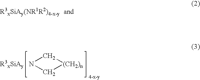
wherein R3 is selected from the group consisting of hydrogen, C1-C4 alkyl, and C1-C4 alkoxy; x is from 0 to 3; Si is silicon; A is halogen; Y is from 0 to 3; N is nitrogen; each of R1 and R2 is same or different and is independently selected from the group consisting of H, aryl, perfluoroaryl, C1-C8 alkyl and C1-C8 perfluoroalkyl; and n is from 1-6. - In a still further embodiment, the present invention relates to a CVD precursor composition for forming a silicon containing thin film on a substrate, such precursor composition including at least one aminosilane source reagent composition selected from the group for forming a silicon containing thin film on a substrate; and
- at least one metalloamide source reagent composition selected from the group consisting of:

wherein M is selected from the group consisting of: Zr, Hf, Y, La, Lanthanide series elements, Ta, Ti, Al; N is nitrogen; each of R1 and R2 is same or different and is independently selected from the group consisting of H, aryl, perfluoroaryl, C1-C8 alkyl, C1-C8 perfluoroalkyl, alkylsilyl; x is the oxidation state on metal M; and n is from 1-6. Preferably, R1 and R2 of the aminosilane and metalloamide source reagent compositions are methyl and/or ethyl. - In one embodiment, the silicon CVD precursor composition of the present invention is used to deposit a metal silicate gate dielectric thin film wherein the silicon precursor is suitably used in combination with at least one dopant precursor, to yield the product metal silicate film. The dopant precursor may advantageously comprise a metalloamide source reagent composition as described herein or may alternatively comprise an alternative dopant source reagent composition as known to those skilled in the art, to deposit metal silicate thin films, (e.g. metal beta-diketonates, metal alkoxides, and metal carboxylates).
- By utilizing a precursor composition including at least one aminosilane source reagent composition and at least one metalloamide source reagent composition to produce a metal silicate dielectric thin film on a substrate, with the metalloamide source reagent composition containing at least part of the metal to be incorporated in the product dielectric metal silicate film, and the aminosilane source reagent compound containing at least part of the silicon to be incorporated in the product dielectric metal silicate film, it is possible by selection of the proportions of such respective compounds to correspondingly vary the stoichiometric composition (metal/silicon ratio) of the metal silicate dielectric film, to obtain a desired character of structural and performance properties in the product film. The relative proportions of the at least one aminosilane source reagent composition and the metalloamide source reagent composition relative to one another are employed to controllably establish the desired Mx/Si1−x ratio in the deposited silicate thin films, wherein MxSi1−x is from about 0.01 to 10. The exact composition will be a trade off between high Si films, which prevent crystallization during subsequent high temperature processing, and high M films, which have higher dielectric constant (lower EOT).
- In one embodiment, the silicon CVD precursor composition of the present invention is used to deposit a silicon nitride barrier layer, wherein the silicon precursor is suitably used in combination with NH3, to yield the product silicon nitride film. The CVD precursor composition may be used in combination with silicon and/or nitrogen sources as readily known to those skilled in the art, to deposit silicon nitride thin films, (e.g., ammonia).
- In a further embodiment, the present invention relates to stable solutions for chemical vapor deposition (CVD) of silicon-containing thin films of varying types, including silicon nitride, silicon dioxide and doped silicon dioxide films (when a dopant co-precursor is utilized), wherein the stable solution comprises at least one aminosilane source reagent composition and at least one solvent component, in which the aminosilane source reagent composition is soluble or suspendable. Accordingly, the aminosilane source reagent composition and the at least one solvent component are combined to produce a precursor solution mixture for depositing a silicon containing thin film on the substrate.
- In a further embodiment, the present invention relates to a CVD multi-component, single source precursor composition useful for forming a metal silicate dielectric thin film on a substrate, such precursor composition including at least one aminosilane source reagent composition as described hereinabove, at least one metalloamide source reagent composition as described hereinabove and a solvent medium in which the aminosilane source reagent composition and the metalloamide source reagent composition are soluble or suspendable, wherein the aminosilane source reagent composition, the metalloamide source reagent composition, and the solvent medium are combined to produce a chemically compatible, single source solution mixture for depositing a silicon containing dielectric thin film on the substrate.
- Providing a precursor composition in liquid (i.e., neat solution or suspension) form facilitates rapid volatilization (i.e., flash vaporization) of the source reagent composition and transport of the resultant precursor vapor to a deposition locus such as a CVD reaction chamber. The aminosilane and metalloamide source reagent compositions of the present invention are chosen to provide a degenerate sweep of ligands, to eliminate ligand exchange and to provide a robust precursor delivery, gas-phase transport and CVD process.
- The precursor compositions of the present invention may comprise any suitable solvent medium that is compatible with the aminosilane and optionally the metalloamide source reagent compositions contained therein. The solvent medium in such respect may comprise a single solvent component, or alternatively a mixture of solvent components. Illustrative solvent media that may be variously usefully employed include ethers, glymes, tetraglymes, amines, polyamines, aliphatic hydrocarbon solvents, aromatic hydrocarbon solvents, cyclic ethers, and compatible combinations of two or more of the foregoing. A particularly preferred solvent species useful in the practice of the present invention is octane. The percentage of the precursor in the solution may range from 0.1 to 99.99% by weight, based on the total weight of the solution.
- The silicon precursor compositions of the invention may be deposited on a wafer or other substrate by use of a CVD system, such systems being well known in the semiconductor fabrication art. Preferred CVD systems include low-pressure CVD systems.
- In a further embodiment the present invention relates to a method for forming a silicon containing thin film on a substrate by chemical vapor deposition, such method including the steps of:
- (1) vaporizing a precursor composition comprising at least one aminosilane source reagent composition made by reacting an aminosilane precursor compound with an amine source reagent compound in a solvent medium comprising at least one activating solvent component, to yield an aminosilane source reagent composition having a halogen content that is less than 1000 ppm, wherein said aminosilane source reagent composition is selected from the group consisting of:

wherein R3 is selected from the group consisting of hydrogen, C 1-C4 alkyl, and C1-C4 alkoxy; x is from 0 to 3; Si is silicon; A is halogen; Y is from 0 to 3; N is nitrogen; each of R1 and R2 is same or different and is independently selected from the group consisting of H, aryl, perfluoroaryl, C1-C8 alkyl, and C1-C8 perfluoroalkyl; and n is from 1-6; - (2) transporting such precursor vapor into a chemical vapor deposition zone containing a substrate, optionally using a carrier gas to effect such transport;
- contacting the precursor vapor with a substrate in such chemical vapor deposition zone, at elevated temperature to deposit a corresponding silicon containing thin film.
- A wide variety of CVD process conditions may be utilized for chemical vapor deposition employing the compositions of the present invention. Typical liquid delivery MOCVD process conditions may include substrate temperature ranges of 160-300° C., with about 170° C. to about 250° C. being more typical; vaporizer temperature ranges may be from about 50° C. to about 150° C., with about 60° C. to about 100° C. being more typical; pressure ranges are generally from about 0.05 to about 20 Torr (and most preferably from about 0.1 to about 5 Torr), with a range of about 0.2 to about 0.5 Torr being more typical; and inert gas flows of helium or argon of from about 25-750 sccm (and most preferably from about 50 to about 200 sccm), at a temperature approximately the same as the vaporizer. In some cases, a co-reactant may be introduced (i.e., water, alcohol or hydrogen forming gas) to facilitate the film growth process.
- The compositions of the present invention are not limited in respect of their use with the aforementioned low-pressure CVD deposition tools, however, and other CVD tools, for example PECVD tools, or other deposition tools, may be utilized.
- In one embodiment the aminosilane source reagent compositions of the instant invention may used in an atomic layer chemical vapor deposition method, wherein the aminosilane source reagent composition is vaporized and introduced into a chemical vapor deposition chamber comprising a substrate, in a sequential or “pulsed” deposition mode, during which time, extremely co-reactive gases may be employed, such as ozone, water vapor or reactive alcohols, that might normally be expected to produce deleterious deposition effects on the CVD process (i.e., gas phase particle formation).
- In a further embodiment, the atomic layer chemical vapor deposition method of the present invention, may further comprise a metalloamide precursor vapor that may be simultaneously co-pulsed and co-deposited with the silicon precursor vapor, on a substrate. Alternatively, the aminosilane precursor vapor may be deposited on a substrate in a sequential pulsing method, wherein the aminosilane compound alternates pulses with the metalloamide compound. The dielectric thin films are built up by introducing short bursts of gases in cycles.
- In a further embodiment, a co-reactant may be used in a pulsed or atomic layer chemical vapor deposition method, wherein the metalloamide precursor and/or aminosilane precursor vapor is separated from the co-reactant by time in the pulse track. The co-reactant may be utilized to facilitate the decomposition of the precursor on a substrate, within a desired temperature regime and to produce carbon-free dielectric thin-films. As an example, the use of water vapor may be utilized to induce a lower decomposition temperature of the aminosilane precursor vapor, which in some instances has been found to be stable in oxidizing environments such as N2O.
- The specific nature of the pulse track and number of cycles may be varied. In a typical ALCVD process, a cycle lasts from 1-5 seconds. The following non-limiting examples demonstrate various pulse tracks defining precursor(s) and co-reactant(s) that may be successfully used to deposit the dielectric thin films of the present invention:
example track 1-(metalloamide/purge (inert)/co-reactant+N2O/purge (inert))n cycles;
example track 2-(metalloamide+aminosilane/purge (inert)/N2O/purge (inert))n cycles;
example track 3-(metalloamide+co-reactant N2O/co-reactant water vapor/purge (inert))n cycles;
example track 4-(metalloamide+co-reactant N2O/aminosilane/co-reactant water vapor/purge (inert))n cycles.
wherein n is an integer number, typically ranging from 10 to 100, and different co-reactants have different oxidizing potentials. - The compositions of the present invention may be delivered to the CVD reactor in a variety of ways. For example, a liquid delivery system may be utilized. Such systems generally include the use of liquid MFCs (mass flow controllers). An exemplary liquid delivery system that may be used is the ATMI Sparta 150 Liquid Delivery System (commercially available from ATMI, Inc., Danbury, Conn.).
- Liquid delivery systems generally meter a desired flow rate of the precursor composition in liquid form to the CVD process tool. At the process tool chamber, or upstream thereof, the liquid may be vaporized through use of a vaporizer. Such vaporizers may utilize thermal heating, acoustics, ultrasound and high flow nebulizers. Further descriptions of liquid delivery systems are contained in U.S. Pat. Nos. 5,204,314; 5,362,328; 5,536,323; and 5,711,816, the disclosures of which are hereby expressly incorporated herein by reference in their entireties.
- In the practice of the present invention utilizing liquid delivery, the silicon precursor species, if of solid or liquid form at ambient conditions, may be dissolved or suspended in a compatible solvent medium as more fully described in U.S. Pat. No. 5,820,664 issued Oct. 13, 1998 for “Precursor Compositions For Chemical Vapor Deposition, And Ligand Exchange Resistant Metal-Organic Precursor Solutions Comprising Same,” the disclosure of which is hereby incorporated herein in its entirety by reference.
- The precursors of the present invention may be deposited using any chemical vapor deposition system known in the art. A preferred liquid delivery MOCVD System is described in U.S. Pat. No. 5,204,314, issued Apr. 20, 1993, for “Method for Delivering an Involatile Reagent in Vapor Form to a CVD Reactor,” the disclosure of which is hereby incorporated herein in its entirety by reference.
- In liquid delivery CVD, the source liquid may comprise the source reagent compound(s) if the compound or complex is in the liquid phase at ambient temperature (e.g., room temperature, 25° C.) or other supply temperature from which the source reagent is rapidly heated and vaporized to form precursor vapor for the CVD process. Alternatively, if the source reagent compound or complex is a solid at ambient or the supply temperature, such compound or complex can be dissolved or suspended in a compatible solvent medium therefore to provide a liquid phase composition that can be submitted to the rapid heating and vaporization to form precursor vapor for the CVD process. The precursor vapor resulting from the vaporization then is transported, optionally in combination with a carrier gas (e.g., He, Ar, H2, O2, etc.), to the chemical vapor deposition reactor where the vapor is contacted with a substrate at elevated temperature to deposit material from the vapor phase onto the substrate or semiconductor device precursor structure positioned in the CVD reactor.
- The precursor liquid may be vaporized in any suitable manner and with any suitable vaporization means to form corresponding precursor vapor for contacting with the elevated temperature substrate on which the dielectric film is to be formed. The vaporization may for example be carried out with a liquid delivery vaporizer unit of a type as commercially available from Advanced Technology Materials, Inc. (Danbury, Conn.) under the trademark SPARTA and VAPORSOURCE II, in which precursor liquid is discharged onto a heated vaporization element, such as a porous sintered metal surface, and flash vaporized. The vaporizer may be arranged to receive a carrier gas such as argon, helium, etc. and an oxygen-containing gas may be introduced as necessary to form the dielectric thin film. The precursor vapor thus is flowed to the chemical vapor deposition chamber and contacted with the substrate on which the dielectric film is to be deposited. The substrate is maintained at a suitable elevated temperature during the deposition operation by heating means such as a radiant heating assembly, a susceptor containing a resistance heating element, microwave heat generator, etc. Appropriate process conditions of temperature, pressure, flow rates and concentration (partial pressures) of metal and silicon components are maintained for sufficient time to form the dielectric film at the desired film thickness, (i.e., in a range of from about 2 nanometers to about 1000 micrometers), and with appropriate dielectric film characteristics.
- The step of vaporizing the source reagent compounds of the present invention is preferably carried out at a vaporization temperature in the range of from about 50° C. to about 300° C. Within this narrow range of vaporization temperature, the metalloamide and aminosilane source reagent compounds are effectively vaporized with a minimum extent of premature decomposition.
- In the optional use of a carrier gas in the practice of the present invention, for transporting the vaporized source reagent composition into the chemical vapor deposition zone, suitable carrier gas species include gases that do not adversely affect the dielectric film being formed on the substrate. Preferred gases include argon, helium, krypton or other inert gas, with argon gas generally being most preferred. In one illustrative embodiment, argon gas may be introduced for mixing with the vaporized source reagent composition at a flow rate of about 100 standard cubic centimeters per minute (sccm).
- Oxidizing gases useful for the broad practice of the present invention include, but are not limited to, O2, N2O, NO, H2O and O3, More preferably, the oxidizer used comprises N2O.
- The deposition of the silicon containing thin films of the present invention are preferably carried out under an elevated deposition temperature in a range of from about 250° C. to about 750° C. By way of example, Hf(NMe2)4 and Si(Me)4 may be mixed in a gas stream, (i.e., in a carrier gas), and mixed in the gas stream to the CVD reactor to produce the appropriate stoichiometry in a deposited HfSiO4 thin-film. Other metalloamides of the invention and silanes may be similarly employed with equivalent success, provided that the respective ligands do not produce undesirable non-degenerate ligand exchanges forming (undesired) new precursor species. It therefore is preferred to use the same ligand species, (i.e., methyl, ethyl, phenyl, etc.) for each of the metalloamide and silicon precursors used in combination with one another.
- By way of further example, Hf(NMe2)4 and Si(NMe)4 may be mixed in a gas stream, (i.e., in a carrier gas), and mixed in the gas stream to the CVD reactor to produce the appropriate stoichiometry in a deposited HfSiO4 thin-film. Other metalloamides of the invention and aminosilanes may be similarly employed with equivalent success, provided that the respective ligands do not produce undesirable non-degenerate ligand exchanges forming (undesired) new precursor species. It therefore is preferred to use the same ligand species, (i.e., methyl, ethyl, phenyl, etc.) for each of the metalloamide and aminosilane precursors used in combination with one another.
- By way of further example, a representative liquid delivery chemical vapor deposition approach is illustrated by the use of metalloamide source reagent compound, Zr(NMe2)4 and aminosilane source reagent compound Si(NMe2)4. The source reagent compounds are introduced into a chemical vapor deposition chamber using liquid delivery and oxidized in-situ to deposit on a substrate, the desired Zr silicate thin film composition based upon electrical performance and film stoichiometry. La(NMe2)4 may be added to the mixture to produce a Zr La doped silicate dielectric film under similar processing conditions.
- By way of further example, a representative liquid delivery chemical vapor deposition approach is illustrated by the use of metalloamide source reagent compound, Y(NMe2)3 and aminosilane source reagent compound Si(NEt2)4. The source reagent compounds are introduced into a chemical vapor deposition chamber using liquid delivery and oxidized in-situ to deposit on a substrate, the desired Y silicate thin film composition based upon electrical performance and film stoichiometry.
- By way of further example, a representative liquid delivery chemical vapor deposition approach is illustrated by the use of metalloamide source reagent compounds Hf(NMe2)4 and La(NMe2)5 and aminosilane source reagent compound Si(NEt2)4. The source reagent compounds are introduced into a chemical vapor deposition chamber using liquid delivery and oxidized in-situ to deposit on a substrate, the desired HfLa silicate thin film composition based upon electrical performance and film stoichiometry. Zr(NMe2)5 may be added to the mixture to produce Zr doped silicate films under similar processing conditions.
- As evidenced hereinabove, it is possible to use respective metalloamides and aminosilane compounds, (i.e., alkyl, and phenyl compounds), regardless of ligand identity and ligand exchange mechanisms, by the use of techniques such as atomic layer or pulsed CVD method, in which the incompatible precursors are separated both temporally and in the introduction lines to limit particle formation and undesired ligand exchange reactions.
- In a further embodiment, the present invention relates to a dielectric thin film, having a dielectric constant value in a range between about 4 to about 60 as measured at a frequency of 1 mega-Hertz, produced by a method comprising the steps of:
-
- vaporizing a precursor composition comprising at least one metalloamide compound of the formula: M(NR1R2)x, as described hereinabove, to form a source reagent precursor vapor;
- transporting such source reagent precursor vapor into a chemical vapor deposition zone containing a substrate, optionally using a carrier gas to effect such transport;
- contacting the source reagent precursor vapor with a substrate in such chemical vapor deposition zone in the presence of an oxidizer and at elevated temperature to deposit a corresponding M containing dielectric thin film.
- In a further embodiment the present invention relates to a silicon containing dielectric thin film, having a dielectric constant in a range between about 4 to about 60 as measured at a frequency of 1 mega-Hertz, by a method comprising the steps:
-
- vaporizing a source reagent precursor composition comprising at least one aminosilane compound of the formula: HxSi(NR1R2)4−x, as described hereinabove, to form a source reagent precursor vapor;
- transporting such source reagent precursor vapor into a chemical vapor deposition zone containing a substrate, optionally using a carrier gas to effect such transport;
- contacting the source reagent precursor vapor with a substrate in such chemical vapor deposition zone in the presence of an oxidizer and at elevated temperature to deposit a corresponding silicate dielectric thin film.
- The dielectric metal silicate thin films produced from the metalloamide materials of the present invention are pure metal silicate thin films comprising little or no carbon or halogen impurity. In a preferred embodiment the dielectric silicate thin films contain less than 1 atomic percent carbon and more preferably the thin films contain less than 1 ppm carbon and no detectable halogen.
- The dielectric silicate films produced in the broad practice of the invention include stoichiometric metal silicate films, as well as off-stoichiometric (metal-deficient) films. Where the precursor composition includes different source reagents providing respectively differential metal and/or silicon content, then the respective source reagents can be supplied in varied compositions to achieve desired stoichiometric characteristics in the corresponding product metal silicate films. In this manner, the electrical properties, including dielectric constant and leakage, can be controlled and closely tailored to a desired end use.
- The dielectric thin films produced by a method of the present invention are useful as, but not limited to: gate dielectric thin films, more particularly metal silicate gate dielectric thin films and metal oxy-nitride gate dielectric thin films; metal oxide high dielectric thin films; and ferroelectric thin films.
- The presence of nitrogen, in at least a partial thickness of the gate dielectric helps to prevent the diffusion of boron, such as from a boron-doped polysilcon gate electrode, to the channel region.
- Exemplary dielectric thin films formed by the method of the present invention include but are not limited to: ZrSiO4; HfSiO4; Ta1−x, AlxOy, where x is 0.03-0.7 and y is 1.5-3; Ta1−xSixOy, where x is 0.05-0.15 and y is 1.5-3; Ta1−x−zAlxSizOy, where 0.7>x+z>0.05, z<0.15 and y is 1.5-3; HfO2; ZrO2; Ta2O5; ZrxSi2−xO4 where x is 0.2-1.6; HfxSi2−xO4, where x is 0.2-1.6; HfxLaySi2−xO4+1.5y, where x is 0.2-1.6 and y is 0-1; ZrxLaySi2−xO4+1.5y, where x is 0.2-1.6 and y is 0-1; HfxAlySi2−xO4+1.5y, where x is 0.2-1.6 and y is 0-0.2; ZrxAlySi2−xO4+1.5y, where x is 0.2-1.6 and y is 0-0.2.
- The use of the compositions disclosed herein is not limited to liquid delivery systems, and any method, which adequately delivers the composition to the process tool is satisfactory. Thus, for example, bubbler-based delivery systems may be utilized, but are not preferred. In such systems, an inert carrier gas is bubbled through the precursor composition (typically in liquid form above its melting point). The resulting gas, which is wholly or partially saturated with the vapor of the composition, is provided to the CVD tool.
- Here and throughout this disclosure, where the invention provides that at least one aminosilane source reagent composition is present in a composition or method, the composition or method may contain or involve additional aminosilane and/or other compounds.
-
Experiment 1 - Silica films were grown with the silicon precursors listed in Table I, Si(NMe2)3Cl and Si(NEt2)2Cl2. Precursor solutions were prepared at 0.1M Si in octane. Substrates of (100) Si were prepared with an SC1 treatment followed by dilute HF to remove any native SiO2. The generic process conditions for the experiments are shown in Table II. Results from the growth of hafnia films encouraged the inventors to center initial experiments on growth in an N2O atmosphere although growth in O2 or other oxidizer could be used at temperatures at or below 500° C. A limited pressure-temperature matrix was performed for each Si precursor using the N2O ambient as shown in
FIGS. 2A and 2B .TABLE I Precursors used for film deposition. (Bis(diethyl-amino)dichlorosilane) Si(N(C2H5)2)2Cl2 (Tris(dimethyl-amino)chlorosilane) Si(N(CH3)2)3Cl Tetrakis(diethyl-amino)hafnium Hf(N(C2H5)2)4 TDEAHf Tetrakis(dimethyl-amino)hafnium Hf(N(CH3)2)4 TDMAHf -
TABLE II Generic process conditions Precursor solution 0.10M in octane Precursor solution delivery rate 0.10 ml/min Vaporization Temperature 150° C. Run time 10 minutes Carrier gas 100 sccm Ar Heating and Cooling process gas 500 sccm Ar Run time process gas 400 sccm N2O Pressure 0.8, 2.2, or 8.0 Torr Temperature 400-650° C. wafer surface - From NMR studies of precursor compatibility, it was shown that Si(NEt2)2Cl2 is compatible with TDEAHf in solution, with any ligand exchange being degenerate. Si(NMe2)3Cl is compatible with both TDEAHf and TDMAHf. A solution of 0.05M TDEAHf: 0.05M Si(NEt2)2Cl2 was produced by mixing the two 0.1M solutions. This mixture was used to grow films over the entire matrix of process conditions.
- Film thickness was measured using single-wavelength ellipsometry at 70° incidence angle, and XRF. For SiO2 deposition, all films were less than 30 Å thick, so an index of refraction could not be measured accurately. Film thickness was assigned based on an assumed index of refraction, n=1.46, typical of high quality thermal oxide. For HfO2, the XRF was calibrated by assuming the X-ray efficiencies were equivalent to TaO2.5, for which standards that been measured by RBS. The Hf:Si composition was estimated by assuming that both are fully oxidized and fully dense. The ellipsometric thickness not accounted for by HfO2 was assigned to SiO2, and composition was calculated from these two thicknesses.
- Results
- Growth rates of SiO2 were less than 3 Å/min under all conditions as shown in
FIG. 3 andFIG. 4 . There is some indication that the Si(NEt2)2Cl2 may form silica films a little bit more readily, however, none of the growth rates are sufficient for the two precursors under the instant conditions. - The growth of SiO2 with only the TDEAHf, as measured by the subtraction of ellipsometric thickness from XRF thickness (shown in
FIG. 5 ) was greater than that from the Si(NEt2)2Cl2 precursor alone (FIG. 3 ) Films grown from the precursor mixture (TDEAHf+Si(NEt2)2Cl2) showed still higher SiO2 growth rates as shown inFIG. 6 . This increased growth rate compared toFIG. 3 is unexpected and should be quite useful for the growth of hafnium silicate films of uniform Hf:Si composition through the thickness of the film. - The films have a mixed Si:Hf composition on the film surface. The constant SiO2 growth rate over the range of 500-600° C. at 2.2 Torr being the same as 0.8 Torr at 600° C. is taken as evidence of mass transport limited deposition over the range of the process. The addition of water vapor or O2, should further decrease the temperature window wherein both Hf and Si alkylamido precursors transport and decompose reliably.
-
Experiment 2 Prior Art Synthetic Process - When attempts were made to synthesize Si(NR2)4 R=Et and Me by combining SiCl4 in hexanes with 5 equivalents of LiNR2, only ClSi(NMe2)3 and Cl2Si(NEt2)2 were obtained.
- Experiment 3 Synthesis of Tetrakis(Dialkylamino) Silanes
- SiCl4 reacts with 5 equivalents of LiNR2 initially in a non-polar solvent, such as hexanes. Then the non-polar solvent is pumped off completely under vacuum. Polar solvent is added into the reaction vessel to continue the reaction. The resulting slurry in polar solvent is refluxed for 4-8 hours to facilitate the completion of the reaction.
-
Experiment 4 Synthesis of Tetrakis(dimethylamino)Silane - The general reactions were carried out under a steady flow of nitrogen. A 5 L Schlenk flask was charged with 0.8 L of 1.6M solution of n-BuLi in hexane, 1 L of anhydrous hexane and a big magnetic stirring bar. Then 60 g (10% excess) of HNMe2 was bubbled into the Schlenk flask slowly at 0° C., under magnetic stirring. During the addition, very fine white precipitate of LiNMe2 was formed and the reaction mixture became extremely viscous. The mixture was allowed to reach room temperature and then was stirred for an additional 2 h. A solution of SiCl4 (43.5 g, 29.3 mL) in hexane (50 mL) was slowly added to the reaction flask. Moderate heat was generated (exothermic) and the external cooling to 0° C. was applied. Upon completion of SiCl4 addition, the mixture became less viscous. The mixture was allowed to reach room temperature and then was stirred for an additional 2 h. All volatiles were removed in vacuum. Then the reaction flask was charge with 0.5 L of anhydrous THF. The resulting mixture was refluxed for 4 h. THF was removed in vacuum to give a slurry-like mixture of Si(NMe2)4 and Li salts. 400 mL of hexane were added to extract Si(NMe2)4 and the resulting mixture was filtered. A second extraction was applied with 100 mL of hexane and a slightly yellow filtrate was obtained. Removal of volatiles under vacuum followed by the vacuum distillation (35° C. at 1 mmHg) gave 31.3 grams of colorless liquid. Yield: 60%. Bp. 35° C. at 1 mmHg. Anal. (calcd., %): C 47.16 (47.06), H 11.42 (11.76), N 26.73 (27.45). Mass spectrum (EI, %): m/z 204 (M+, 70), 160 (M+−NMe2, 100), 116 (M+−2 NMe2, 90).
FIG. 7 1H NMR (C6D6):2.51 (s, CH3). Residual Cl content is less than 10 ppm (detection limit of analysis).
-
Experiment 4 Synthesis of Tetrakis(ethylmethylamino)Silane - A 5 L Schlenk flask was charged with 0.8 L of 1.6M solution of n-BuLi in hexane, 1 L of anhydrous hexane and a big magnetic stirring bar. The reaction mixture was maintained at 0° C. during the addition of HNEtMe (79.3 g, 1.344 mol, 5% excess) solution in hexane (100 mL). Very fine white precipitate of LiNEtMe formed immediately and the reaction mixture became extremely viscous. The mixture was allowed to reach room temperature and then was stirred for an additional hour. A solution of HSiCl3 (43.36 g, 0.32 mol) in hexane (100 mL) was slowly added to the reaction flask. Moderate heat was generated (exothermic) and the external cooling to 0° C. was applied. Upon completion of HSiCl3 addition, the mixture became less viscous. The mixture was allowed to reach room temperature and then was stirred for an additional hour. All volatiles were removed in vacuum. Then the reaction flask was charge with 0.5 L of anhydrous THF. The resulting mixture was refluxed for 4 h. THF was removed in vacuum. 300 mL of hexane were added to extract amidosilanes, the resulting mixture was filtered, and the precipitate was discarded. Removal of volatiles under vacuum followed by the vacuum distillation gave two fractions (28° C. at 0.5 mmHg and 50° C. at 0.3 mmHg) in 4:3 molar rations. The first fraction was confirmed to be HSi(NEtMe)3. The second fraction was identified as Si(NEtMe)4. Yield: 30%. Bp. 50° C. at 0.3 mmHg. Anal. (calcd., %): C 55.61 (55.38), H 12.58 (12.31), N 21.08 (21.54). Mass spectrum (EI, %): m/z 260 (M+, 40), 202 (M+−NEtMe, 70), 144 (M+−2 NEtMe, 50), 86 (M+−3 NEtMe, 100). 1H NMR (C6D6): □ 2.83 (8 H, q, J(H—H)=7 Hz, CH 2CH3) 2.51 (12H, s, CH 3), 1.07 (12H, t, J(H—H)=7 Hz, CH2CH 3). 13C NMR: (C6D6) □ 44.68 (CH2—CH3) 35.07 (CH3), 15.01 (CH2—CH3).
- The features, aspects and advantages of the present invention are further shown with reference to the following non-limiting examples relating to the invention.
Claims (37)
1. A liquid CVD precursor composition for forming a thin film dielectric on a substrate, such precursor composition including at least one metalloamide source reagent compound having a formula:
M(NR2)x(NR′2)y
wherein M is selected from the group consisting of: Y, Hf, La, and Ta; N is nitrogen, each of R and R1 is independently selected from the group consisting of H, aryl, perfluoroaryl, C1-C8 alkyl, C1-C8 perfluoroalkyl, and alkylsilyl; (NR2)x and (NR′2) are different amino ligands and R′ is different from R; x is from 1 to 5; y is from 1 to 5; and x+y is equal to the oxidation state of metal M, and a solvent medium, wherein the metalloamide source reagent compound is soluble or suspendable therein.
2. The liquid CVD precursor composition of claim 1 , wherein the precursor composition further comprises an aminosilane source reagent compound of the formula:
HxSi(NR1R2)4−x
wherein H is hydrogen; x is from 0 to 3; Si is silicon; N is nitrogen; each of R1 and R2 is same or different and is independently selected from the group consisting of H, aryl, perfluoroaryl, C1-C8 alkyl, and C1-C8 perfluoroalkyl.
3. The liquid CVD precursor composition of claim 1 , wherein the CVD precursor composition further comprises a vapor source reagent compound selected from the group consisting of silane, trimethylsilane, tetramethylsilane, tetraethylorthosilicate.
4. A CVD method of forming a dielectric thin film on a substrate, comprising:
vaporizing the liquid CVD precursor composition of claim 1 to form a source reagent precursor vapor;
transporting the source reagent precursor vapor into a chemical vapor deposition zone, optionally using a carrier gas; and
contacting the source reagent precursor vapor with a substrate in said chemical vapor deposition zone at elevated temperature to deposit a dielectric thin film on the substrate.
5. The CVD method according to claim 4 , wherein the liquid CVD precursor composition is vaporized in a liquid delivery apparatus.
6. The CVD method according to claim 4 , wherein the source reagent precursor vapor is transported into the chemical vapor deposition zone in a pulsed deposition mode.
7. The CVD method according to claim 4 , wherein the dielectric thin film is deposited in the absence of an oxidizer.
8. The CVD method according to claim 4 , wherein the liquid CVD precursor composition further comprises an aminosilane source reagent compound.
9. The CVD method of claim 8 , wherein the aminosilane source reagent compound has the formula:
HxSi(NR1R2)4−x
wherein H is hydrogen; x is from 0 to 3; Si is silicon; N is nitrogen; each of R1 and R2 is same or different and is independently selected from the group consisting of H, aryl, perfluoroaryl, C1-C8 alkyl, and C1-C8 perfluoroalkyl.
10. The CVD method of claim 4 , further comprising contacting the source reagent precursor vapor with the substrate in said chemical vapor deposition zone in the presence of an oxidizer at elevated temperature to form the dielectric thin film on the substrate.
11. The CVD method according to claim 10 , wherein the oxidizing gas is selected from the group consisting of: O2, N2O, NO and O3.
12. The CVD method according to claim 4 , wherein the chemical vapor deposition zone is at a temperature in the range of from about 350° C. to about 750° C.
13. A method of forming a dielectric thin film on a substrate, comprising:
vaporizing a source reagent precursor composition mixture comprising the liquid CVD precursor composition of claim 1 and at least one aminosilane precursor, to form a source reagent precursor vapor;
transporting the source reagent precursor vapor into a chemical vapor deposition zone, optionally using a carrier gas;
contacting the source reagent precursor vapor with a substrate in said chemical vapor deposition zone at elevated temperature to deposit a dielectric thin film on the substrate.
14. A method of manufacturing a microelectronic device comprising a substrate having a dielectric thin film thereon, said method comprising:
vaporizing the liquid CVD precursor composition of claim 1 to form a source reagent precursor vapor;
transporting the source reagent precursor vapor into a chemical vapor deposition zone, optionally using a carrier gas; and
contacting the source reagent precursor vapor with a substrate in said chemical vapor deposition zone at elevated temperature to deposit a dielectric thin film on the substrate thereby forming said substrate having said dielectric thin film thereon.
15. The method according to claim 13 , wherein the liquid CVD precursor composition further comprises an aminosilane source reagent compound.
16. The method of claim 14 , wherein the aminosilane source reagent compound has the formula:
HxSi(NR1R2)4−x
wherein H is hydrogen; x is from 0 to 3; Si is silicon; N is nitrogen; each of R1 and R2 is same or different and is independently selected from the group consisting of H, aryl, perfluoroaryl, C1-C8 alkyl, and C1-C8 perfluoroalkyl.
17. A method of synthesizing an aminosilane source reagent composition, comprising:

(a) reacting an aminosilane precursor compound with an amine source reagent compound, wherein the amine source reagent compound is selected from the group consisting of:
wherein B is selected from the group consisting of H, Li, Na, K, Zn and MgBr; N is nitrogen; R1 and R2 are same or different and each is independently selected from the group consisting of H, aryl, perfluoroaryl, C1-C8 alkyl, and C1-C8 perfluoroalkyl; and n is from 1-6, in a solvent system comprising at least one non-polar solvent, at temperature in a range from about −30° C. to about room temperature, for a period of time sufficient to produce a reaction mixture comprising partially substituted aminosilane components, unreacted aminosilane precursors and unreacted amine components;
(b) combining the reaction mixture with at least one polar activating solvent component to at least partially solvate and activate the unreacted amine components; and
(c) continuing the reaction of step (b) at temperature in a range from about 0° C. to about 100° C. for a period of time sufficient to produce the aminosilane source reagent composition, wherein the aminosilane source reagent composition comprises less than 1000 ppm halogen.
18. The method of claim 17 , further comprising (d) separating the aminosilane source reagent composition from a by-product of the reaction mixture.
19. The method of claim 18 , further comprising (e) purifying the separated aminosilane source reagent composition.
20. The method of claim 19 , wherein the aminosilane source reagent composition is purified by distillation.
21. The method of claim 19 , further comprising (f) redissolving the purified aminosilane source reagent composition in a suitable solvent medium.
22. The method of claim 21 , wherein the suitable solvent medium comprises an organic solvent selected from the group consisting of ethers, glymes, tetraglymes, amines, polyamines, aliphatic hydrocarbons, aromatic hydrocarbons, cyclic ethers, and compatible combinations of two or more of the foregoing.
23. A method of synthesizing an aminosilane source reagent composition, comprising the steps of:
(1) combining an aminosilane precursor compound comprising at least one halogen leaving group, with an amine source reagent compound, in a solvent system comprising at least one non-polar solvent, for a period of time sufficient to produce a reaction mixture consisting essentially of partially substituted aminosilane components, unreacted aminosilane precursors and unreacted amine components;
(2) combining with the reaction mixture of step (1) a polar activating solvent to at least partially solvate and activate the unreacted amine components;
(3) continuing the reaction of step (2) for a period of time sufficient to provide for essentially stoichiometric substitution of at least one halide on the aminosilane precursor compound by an amine component to produce the aminosilane source reagent composition, further comprising (4) separating the aminosilane source reagent composition from a by-product of the reaction mixture.
24. The method of claim 23 , further comprising (5) purifying the separated aminosilane source reagent composition.
25. The method of claim 24 , wherein the aminosilane source reagent composition is purified by distillation.
26. The method of claim 24 , further comprising (6) redissolving the purified aminosilane source reagent composition in a suitable solvent medium.
27. The method of claim 26 , wherein the suitable solvent medium comprises an organic solvent selected from the group consisting of ethers, glymes, tetraglymes, amines, polyamines, aliphatic hydrocarbons, aromatic hydrocarbons, cyclic ethers, and compatible combinations of two or more of the foregoing.
28. A method of synthesizing an aminosilane source reagent composition, comprising the steps of:
(1) combining an aminosilane precursor compound comprising at least one halogen leaving group, with an amine source reagent compound, in a solvent system comprising at least one non-polar solvent, for a period of time sufficient to produce a reaction mixture consisting essentially of partially substituted aminosilane components, unreacted aminosilane precursors and unreacted amine components;
(2) removing the non-polar solvent from the reaction mixture;
(3) combining with the reaction mixture of step (2) a polar activating solvent to at least partially solvate and activate the unreacted amine components;
(4) continuing the reaction of step (3) for a period of time sufficient to provide for essentially stoichiometric substitution of at least one halide on the aminosilane precursor compound by an amine component to produce the aminosilane source reagent composition, further comprising (5) separating the aminosilane source reagent composition from a by-product of the reaction mixture.
29. The method of claim 28 , further comprising (6) purifying the separated aminosilane source reagent composition.
30. The method of claim 29 , wherein the aminosilane source reagent composition is purified by distillation.
31. The method of claim 29 , further comprising (7) redissolving the purified aminosilane source reagent composition in a suitable solvent medium.
32. The method of claim 31 , wherein the suitable solvent medium comprises an organic solvent selected from the group consisting of ethers, glymes, tetraglymes, amines, polyamines, aliphatic hydrocarbons, aromatic hydrocarbons, cyclic ethers, and compatible combinations of two or more of the foregoing.
33. The method according to claim 17 , wherein the aminosilane source reagent composition is selected from the group consisting of: Si(NMe2)3Cl, Si(NEt2)2Cl2, Si(NMe2)4, Si(NEt2)4 and Si(NMeEt)4.
34. The method according to claim 28 , wherein the aminosilane source reagent composition is selected from the group consisting of: Si(NMe2)3Cl, Si(NEt2)2Cl2, Si(NMe2)4Si(NEt2)4 and Si(NMeEt)4.
35. The method according to claim 17 , wherein the aminosilane source reagent composition comprises Si(NMe2)4.
36. The method according to claim 23 , wherein the aminosilane source reagent composition comprises Si(NMe2)4.
37. The method according to claim 28 , wherein the aminosilane source reagent composition comprises Si(NMe2)4.
Priority Applications (1)
| Application Number | Priority Date | Filing Date | Title |
|---|---|---|---|
| US11/363,904 US20060148271A1 (en) | 2001-03-30 | 2006-02-28 | Silicon source reagent compositions, and method of making and using same for microelectronic device structure |
Applications Claiming Priority (4)
| Application Number | Priority Date | Filing Date | Title |
|---|---|---|---|
| US09/823,196 US7005392B2 (en) | 2001-03-30 | 2001-03-30 | Source reagent compositions for CVD formation of gate dielectric thin films using amide precursors and method of using same |
| US09/954,831 US6869638B2 (en) | 2001-03-30 | 2001-09-18 | Source reagent compositions for CVD formation of gate dielectric thin films using amide precursors and method of using same |
| US10/112,517 US7084080B2 (en) | 2001-03-30 | 2002-03-29 | Silicon source reagent compositions, and method of making and using same for microelectronic device structure |
| US11/363,904 US20060148271A1 (en) | 2001-03-30 | 2006-02-28 | Silicon source reagent compositions, and method of making and using same for microelectronic device structure |
Related Parent Applications (3)
| Application Number | Title | Priority Date | Filing Date |
|---|---|---|---|
| US09/823,196 Continuation US7005392B2 (en) | 2001-03-30 | 2001-03-30 | Source reagent compositions for CVD formation of gate dielectric thin films using amide precursors and method of using same |
| US09/954,831 Continuation US6869638B2 (en) | 2001-03-30 | 2001-09-18 | Source reagent compositions for CVD formation of gate dielectric thin films using amide precursors and method of using same |
| US10/112,517 Continuation US7084080B2 (en) | 2001-03-30 | 2002-03-29 | Silicon source reagent compositions, and method of making and using same for microelectronic device structure |
Publications (1)
| Publication Number | Publication Date |
|---|---|
| US20060148271A1 true US20060148271A1 (en) | 2006-07-06 |
Family
ID=25238064
Family Applications (3)
| Application Number | Title | Priority Date | Filing Date |
|---|---|---|---|
| US09/823,196 Expired - Fee Related US7005392B2 (en) | 2001-03-30 | 2001-03-30 | Source reagent compositions for CVD formation of gate dielectric thin films using amide precursors and method of using same |
| US09/954,831 Expired - Lifetime US6869638B2 (en) | 2001-03-30 | 2001-09-18 | Source reagent compositions for CVD formation of gate dielectric thin films using amide precursors and method of using same |
| US11/363,904 Abandoned US20060148271A1 (en) | 2001-03-30 | 2006-02-28 | Silicon source reagent compositions, and method of making and using same for microelectronic device structure |
Family Applications Before (2)
| Application Number | Title | Priority Date | Filing Date |
|---|---|---|---|
| US09/823,196 Expired - Fee Related US7005392B2 (en) | 2001-03-30 | 2001-03-30 | Source reagent compositions for CVD formation of gate dielectric thin films using amide precursors and method of using same |
| US09/954,831 Expired - Lifetime US6869638B2 (en) | 2001-03-30 | 2001-09-18 | Source reagent compositions for CVD formation of gate dielectric thin films using amide precursors and method of using same |
Country Status (5)
| Country | Link |
|---|---|
| US (3) | US7005392B2 (en) |
| EP (1) | EP1373278A4 (en) |
| JP (2) | JP2004529495A (en) |
| KR (2) | KR20090009989A (en) |
| WO (1) | WO2002079211A1 (en) |
Cited By (17)
| Publication number | Priority date | Publication date | Assignee | Title |
|---|---|---|---|---|
| US20060099831A1 (en) * | 2001-03-30 | 2006-05-11 | Borovik Alexander S | Silicon source reagent compositions, and method of making and using same for microelectronic device structure |
| US20070190768A1 (en) * | 2006-01-31 | 2007-08-16 | Motoyuki Sato | Manufacturing method of semiconductor device |
| US20080026577A1 (en) * | 2006-07-31 | 2008-01-31 | Rohm And Haas Electronic Materials Llc | Organometallic compounds |
| US20080145535A1 (en) * | 2006-12-13 | 2008-06-19 | Air Products And Chemicals, Inc. | Cyclic Chemical Vapor Deposition of Metal-Silicon Containing Films |
| US20090079015A1 (en) * | 2007-09-26 | 2009-03-26 | Micron Technology, Inc. | Lanthanide dielectric with controlled interfaces |
| US20100164057A1 (en) * | 2007-06-28 | 2010-07-01 | Advanced Technology Materials, Inc. | Precursors for silicon dioxide gap fill |
| US7750173B2 (en) | 2007-01-18 | 2010-07-06 | Advanced Technology Materials, Inc. | Tantalum amido-complexes with chelate ligands useful for CVD and ALD of TaN and Ta205 thin films |
| US20120021127A1 (en) * | 2009-03-19 | 2012-01-26 | Adeka Corporation | Material for chemical vapor deposition and process for forming silicon-containing thin film using same |
| US20140273477A1 (en) * | 2013-03-14 | 2014-09-18 | Asm Ip Holding B.V. | Si PRECURSORS FOR DEPOSITION OF SiN AT LOW TEMPERATURES |
| US9362109B2 (en) | 2013-10-16 | 2016-06-07 | Asm Ip Holding B.V. | Deposition of boron and carbon containing materials |
| US9401273B2 (en) | 2013-12-11 | 2016-07-26 | Asm Ip Holding B.V. | Atomic layer deposition of silicon carbon nitride based materials |
| US9576792B2 (en) | 2014-09-17 | 2017-02-21 | Asm Ip Holding B.V. | Deposition of SiN |
| US9576790B2 (en) | 2013-10-16 | 2017-02-21 | Asm Ip Holding B.V. | Deposition of boron and carbon containing materials |
| US9824881B2 (en) | 2013-03-14 | 2017-11-21 | Asm Ip Holding B.V. | Si precursors for deposition of SiN at low temperatures |
| US10410857B2 (en) | 2015-08-24 | 2019-09-10 | Asm Ip Holding B.V. | Formation of SiN thin films |
| US10580645B2 (en) | 2018-04-30 | 2020-03-03 | Asm Ip Holding B.V. | Plasma enhanced atomic layer deposition (PEALD) of SiN using silicon-hydrohalide precursors |
| US11056353B2 (en) | 2017-06-01 | 2021-07-06 | Asm Ip Holding B.V. | Method and structure for wet etch utilizing etch protection layer comprising boron and carbon |
Families Citing this family (151)
| Publication number | Priority date | Publication date | Assignee | Title |
|---|---|---|---|---|
| US7012292B1 (en) * | 1998-11-25 | 2006-03-14 | Advanced Technology Materials, Inc | Oxidative top electrode deposition process, and microelectronic device structure |
| US6273951B1 (en) | 1999-06-16 | 2001-08-14 | Micron Technology, Inc. | Precursor mixtures for use in preparing layers on substrates |
| US6156743A (en) * | 1999-10-18 | 2000-12-05 | Whitcomb; John E. | Method of decreasing fatigue |
| US6620723B1 (en) | 2000-06-27 | 2003-09-16 | Applied Materials, Inc. | Formation of boride barrier layers using chemisorption techniques |
| US6969539B2 (en) | 2000-09-28 | 2005-11-29 | President And Fellows Of Harvard College | Vapor deposition of metal oxides, silicates and phosphates, and silicon dioxide |
| US6528374B2 (en) * | 2001-02-05 | 2003-03-04 | International Business Machines Corporation | Method for forming dielectric stack without interfacial layer |
| US7005392B2 (en) * | 2001-03-30 | 2006-02-28 | Advanced Technology Materials, Inc. | Source reagent compositions for CVD formation of gate dielectric thin films using amide precursors and method of using same |
| EP1256638B1 (en) * | 2001-05-07 | 2008-03-26 | Samsung Electronics Co., Ltd. | Method of forming a multi-components thin film |
| US7037862B2 (en) | 2001-06-13 | 2006-05-02 | Micron Technology, Inc. | Dielectric layer forming method and devices formed therewith |
| US6391803B1 (en) * | 2001-06-20 | 2002-05-21 | Samsung Electronics Co., Ltd. | Method of forming silicon containing thin films by atomic layer deposition utilizing trisdimethylaminosilane |
| US7164169B2 (en) * | 2001-08-23 | 2007-01-16 | Nec Corporation | Semiconductor device having high-permittivity insulation film and production method therefor |
| US20030111678A1 (en) * | 2001-12-14 | 2003-06-19 | Luigi Colombo | CVD deposition of M-SION gate dielectrics |
| JP4102072B2 (en) * | 2002-01-08 | 2008-06-18 | 株式会社東芝 | Semiconductor device |
| US6846516B2 (en) | 2002-04-08 | 2005-01-25 | Applied Materials, Inc. | Multiple precursor cyclical deposition system |
| US6656764B1 (en) * | 2002-05-15 | 2003-12-02 | Taiwan Semiconductor Manufacturing Company | Process for integration of a high dielectric constant gate insulator layer in a CMOS device |
| JP3627106B2 (en) * | 2002-05-27 | 2005-03-09 | 株式会社高純度化学研究所 | Method for producing hafnium silicate thin film by atomic layer adsorption deposition |
| US7067439B2 (en) * | 2002-06-14 | 2006-06-27 | Applied Materials, Inc. | ALD metal oxide deposition process using direct oxidation |
| US20030232501A1 (en) | 2002-06-14 | 2003-12-18 | Kher Shreyas S. | Surface pre-treatment for enhancement of nucleation of high dielectric constant materials |
| US6858547B2 (en) | 2002-06-14 | 2005-02-22 | Applied Materials, Inc. | System and method for forming a gate dielectric |
| WO2004009861A2 (en) * | 2002-07-19 | 2004-01-29 | Asm America, Inc. | Method to form ultra high quality silicon-containing compound layers |
| GB2391555A (en) * | 2002-08-09 | 2004-02-11 | Epichem Ltd | Vapour phase deposition of silicate and oxide films |
| TW200408015A (en) * | 2002-08-18 | 2004-05-16 | Asml Us Inc | Atomic layer deposition of high K metal silicates |
| EP1535321A4 (en) * | 2002-08-18 | 2009-05-27 | Asml Us Inc | Low termperature deposition of silicon oxides and oxynitrides |
| TW200408323A (en) * | 2002-08-18 | 2004-05-16 | Asml Us Inc | Atomic layer deposition of high k metal oxides |
| US6958300B2 (en) * | 2002-08-28 | 2005-10-25 | Micron Technology, Inc. | Systems and methods for forming metal oxides using metal organo-amines and metal organo-oxides |
| US7087481B2 (en) * | 2002-08-28 | 2006-08-08 | Micron Technology, Inc. | Systems and methods for forming metal oxides using metal compounds containing aminosilane ligands |
| US8617312B2 (en) * | 2002-08-28 | 2013-12-31 | Micron Technology, Inc. | Systems and methods for forming layers that contain niobium and/or tantalum |
| US6984592B2 (en) * | 2002-08-28 | 2006-01-10 | Micron Technology, Inc. | Systems and methods for forming metal-doped alumina |
| US7112485B2 (en) | 2002-08-28 | 2006-09-26 | Micron Technology, Inc. | Systems and methods for forming zirconium and/or hafnium-containing layers |
| US7253122B2 (en) * | 2002-08-28 | 2007-08-07 | Micron Technology, Inc. | Systems and methods for forming metal oxides using metal diketonates and/or ketoimines |
| US7041609B2 (en) * | 2002-08-28 | 2006-05-09 | Micron Technology, Inc. | Systems and methods for forming metal oxides using alcohols |
| US7033560B2 (en) | 2002-08-30 | 2006-04-25 | Air Products And Chemicals, Inc. | Single source mixtures of metal siloxides |
| US6624093B1 (en) * | 2002-10-09 | 2003-09-23 | Wisys Technology Foundation | Method of producing high dielectric insulator for integrated circuit |
| KR100463633B1 (en) * | 2002-11-12 | 2004-12-29 | 주식회사 아이피에스 | Method for depositing thin film on wafer using Hafnium compound |
| JP4907839B2 (en) * | 2003-03-26 | 2012-04-04 | ルネサスエレクトロニクス株式会社 | Manufacturing method of semiconductor device |
| JP4954448B2 (en) * | 2003-04-05 | 2012-06-13 | ローム・アンド・ハース・エレクトロニック・マテリアルズ,エル.エル.シー. | Organometallic compounds |
| JP4714422B2 (en) * | 2003-04-05 | 2011-06-29 | ローム・アンド・ハース・エレクトロニック・マテリアルズ,エル.エル.シー. | Method for depositing germanium-containing film and vapor delivery device |
| TW200506093A (en) * | 2003-04-21 | 2005-02-16 | Aviza Tech Inc | System and method for forming multi-component films |
| US7199061B2 (en) * | 2003-04-21 | 2007-04-03 | Applied Materials, Inc. | Pecvd silicon oxide thin film deposition |
| US20050070126A1 (en) * | 2003-04-21 | 2005-03-31 | Yoshihide Senzaki | System and method for forming multi-component dielectric films |
| US7115528B2 (en) | 2003-04-29 | 2006-10-03 | Micron Technology, Inc. | Systems and method for forming silicon oxide layers |
| US20040245602A1 (en) * | 2003-05-21 | 2004-12-09 | Kim Sun Jung | Method of fabricating metal-insulator-metal capacitor (MIM) using lanthanide-doped HfO2 |
| US7141500B2 (en) * | 2003-06-05 | 2006-11-28 | American Air Liquide, Inc. | Methods for forming aluminum containing films utilizing amino aluminum precursors |
| KR100560666B1 (en) * | 2003-07-07 | 2006-03-16 | 삼성전자주식회사 | Metal layer deposition system for semiconductor device fabrication and method of operating the same |
| US7208427B2 (en) * | 2003-08-18 | 2007-04-24 | Advanced Technology Materials, Inc. | Precursor compositions and processes for MOCVD of barrier materials in semiconductor manufacturing |
| JP3956225B2 (en) * | 2003-08-26 | 2007-08-08 | 株式会社トリケミカル研究所 | Film formation method |
| US7303996B2 (en) * | 2003-10-01 | 2007-12-04 | Taiwan Semiconductor Manufacturing Co., Ltd. | High-K gate dielectric stack plasma treatment to adjust threshold voltage characteristics |
| US6960675B2 (en) * | 2003-10-14 | 2005-11-01 | Advanced Technology Materials, Inc. | Tantalum amide complexes for depositing tantalum-containing films, and method of making same |
| US20050214458A1 (en) * | 2004-03-01 | 2005-09-29 | Meiere Scott H | Low zirconium hafnium halide compositions |
| US20060062910A1 (en) * | 2004-03-01 | 2006-03-23 | Meiere Scott H | Low zirconium, hafnium-containing compositions, processes for the preparation thereof and methods of use thereof |
| JP4526995B2 (en) * | 2004-04-09 | 2010-08-18 | 東京エレクトロン株式会社 | Method for forming gate insulating film, computer-readable storage medium, and computer program |
| US20050252449A1 (en) | 2004-05-12 | 2005-11-17 | Nguyen Son T | Control of gas flow and delivery to suppress the formation of particles in an MOCVD/ALD system |
| US20060062917A1 (en) * | 2004-05-21 | 2006-03-23 | Shankar Muthukrishnan | Vapor deposition of hafnium silicate materials with tris(dimethylamino)silane |
| US8119210B2 (en) | 2004-05-21 | 2012-02-21 | Applied Materials, Inc. | Formation of a silicon oxynitride layer on a high-k dielectric material |
| US8323754B2 (en) | 2004-05-21 | 2012-12-04 | Applied Materials, Inc. | Stabilization of high-k dielectric materials |
| US6987063B2 (en) * | 2004-06-10 | 2006-01-17 | Freescale Semiconductor, Inc. | Method to reduce impurity elements during semiconductor film deposition |
| US7253084B2 (en) * | 2004-09-03 | 2007-08-07 | Asm America, Inc. | Deposition from liquid sources |
| US7966969B2 (en) * | 2004-09-22 | 2011-06-28 | Asm International N.V. | Deposition of TiN films in a batch reactor |
| US7332618B2 (en) * | 2004-09-28 | 2008-02-19 | Praxair Technology, Inc. | Organometallic precursor compounds |
| US7723245B2 (en) * | 2004-11-29 | 2010-05-25 | Hitachi Kokusai Electric Inc. | Method for manufacturing semiconductor device, and substrate processing apparatus |
| KR100632460B1 (en) * | 2005-02-03 | 2006-10-11 | 삼성전자주식회사 | Method for fabricating semiconductor device |
| US7629267B2 (en) * | 2005-03-07 | 2009-12-08 | Asm International N.V. | High stress nitride film and method for formation thereof |
| TW200731404A (en) * | 2005-04-07 | 2007-08-16 | Aviza Tech Inc | Multilayer, multicomponent high-k films and methods for depositing the same |
| US7514119B2 (en) * | 2005-04-29 | 2009-04-07 | Linde, Inc. | Method and apparatus for using solution based precursors for atomic layer deposition |
| US7425350B2 (en) * | 2005-04-29 | 2008-09-16 | Asm Japan K.K. | Apparatus, precursors and deposition methods for silicon-containing materials |
| US9312557B2 (en) * | 2005-05-11 | 2016-04-12 | Schlumberger Technology Corporation | Fuel cell apparatus and method for downhole power systems |
| US7875556B2 (en) | 2005-05-16 | 2011-01-25 | Air Products And Chemicals, Inc. | Precursors for CVD silicon carbo-nitride and silicon nitride films |
| US7402534B2 (en) | 2005-08-26 | 2008-07-22 | Applied Materials, Inc. | Pretreatment processes within a batch ALD reactor |
| US7521356B2 (en) * | 2005-09-01 | 2009-04-21 | Micron Technology, Inc. | Atomic layer deposition systems and methods including silicon-containing tantalum precursor compounds |
| KR100715522B1 (en) * | 2005-11-02 | 2007-05-07 | 엠텍비젼 주식회사 | Camera control apparatus, image data displaying apparatus and method thereof |
| KR100724084B1 (en) * | 2005-11-16 | 2007-06-04 | 주식회사 유피케미칼 | Thin film deposition from atomic layer deposition or chemical vapor deposition and their uses |
| WO2007075369A1 (en) * | 2005-12-16 | 2007-07-05 | Asm International N.V. | Low temperature doped silicon layer formation |
| KR100762238B1 (en) * | 2006-03-21 | 2007-10-01 | 주식회사 하이닉스반도체 | Transistor of semiconductor device and method of fabricating the same |
| US7798096B2 (en) | 2006-05-05 | 2010-09-21 | Applied Materials, Inc. | Plasma, UV and ion/neutral assisted ALD or CVD in a batch tool |
| WO2007133837A2 (en) | 2006-05-12 | 2007-11-22 | Advanced Technology Materials, Inc. | Low temperature deposition of phase change memory materials |
| US7875312B2 (en) * | 2006-05-23 | 2011-01-25 | Air Products And Chemicals, Inc. | Process for producing silicon oxide films for organoaminosilane precursors |
| US8530361B2 (en) * | 2006-05-23 | 2013-09-10 | Air Products And Chemicals, Inc. | Process for producing silicon and oxide films from organoaminosilane precursors |
| US7582574B2 (en) | 2006-05-30 | 2009-09-01 | Air Products And Chemicals, Inc. | Diethylsilane as a silicon source in the deposition of metal silicate films |
| US8399056B2 (en) * | 2006-06-02 | 2013-03-19 | L'Air Liquide, Société Anonyme pour l'Etude et l'Exploitation des Procédés Georges Claude | Method of forming high-k dielectric films based on novel titanium, zirconium, and hafnium precursors and their use for semiconductor manufacturing |
| US7691757B2 (en) | 2006-06-22 | 2010-04-06 | Asm International N.V. | Deposition of complex nitride films |
| US8318966B2 (en) | 2006-06-23 | 2012-11-27 | Praxair Technology, Inc. | Organometallic compounds |
| US7956168B2 (en) * | 2006-07-06 | 2011-06-07 | Praxair Technology, Inc. | Organometallic compounds having sterically hindered amides |
| WO2008010941A2 (en) * | 2006-07-20 | 2008-01-24 | The Boc Group, Inc. | Improved methods for atomic layer deposition |
| US7795160B2 (en) * | 2006-07-21 | 2010-09-14 | Asm America Inc. | ALD of metal silicate films |
| US7956207B2 (en) * | 2006-09-28 | 2011-06-07 | Praxair Technology, Inc. | Heteroleptic organometallic compounds |
| US7713854B2 (en) * | 2006-10-20 | 2010-05-11 | Taiwan Semiconductor Manufacturing Co., Ltd. | Gate dielectric layers and methods of fabricating gate dielectric layers |
| KR101279925B1 (en) | 2006-11-02 | 2013-07-08 | 어드밴스드 테크놀러지 머티리얼즈, 인코포레이티드 | Antimony and germanium complexes useful for cvd/ald of metal thin films |
| TW200831694A (en) * | 2007-01-17 | 2008-08-01 | Advanced Tech Materials | Precursor compositions for ALD/CVD of group II ruthenate thin films |
| US20080207007A1 (en) | 2007-02-27 | 2008-08-28 | Air Products And Chemicals, Inc. | Plasma Enhanced Cyclic Chemical Vapor Deposition of Silicon-Containing Films |
| JP4845782B2 (en) * | 2007-03-16 | 2011-12-28 | 東京エレクトロン株式会社 | Film forming raw material |
| US20100112211A1 (en) * | 2007-04-12 | 2010-05-06 | Advanced Technology Materials, Inc. | Zirconium, hafnium, titanium, and silicon precursors for ald/cvd |
| US7629256B2 (en) * | 2007-05-14 | 2009-12-08 | Asm International N.V. | In situ silicon and titanium nitride deposition |
| US20100209610A1 (en) * | 2007-07-16 | 2010-08-19 | Advanced Technology Materials, Inc. | Group iv complexes as cvd and ald precursors for forming metal-containing thin films |
| KR101458953B1 (en) | 2007-10-11 | 2014-11-07 | 삼성전자주식회사 | Method of forming phase change material layer using Ge(Ⅱ) source, and method of fabricating phase change memory device |
| US8834968B2 (en) | 2007-10-11 | 2014-09-16 | Samsung Electronics Co., Ltd. | Method of forming phase change material layer using Ge(II) source, and method of fabricating phase change memory device |
| SG178736A1 (en) * | 2007-10-31 | 2012-03-29 | Advanced Tech Materials | Amorphous ge/te deposition process |
| US20090130414A1 (en) * | 2007-11-08 | 2009-05-21 | Air Products And Chemicals, Inc. | Preparation of A Metal-containing Film Via ALD or CVD Processes |
| US8016945B2 (en) * | 2007-12-21 | 2011-09-13 | Applied Materials, Inc. | Hafnium oxide ALD process |
| US20090215225A1 (en) | 2008-02-24 | 2009-08-27 | Advanced Technology Materials, Inc. | Tellurium compounds useful for deposition of tellurium containing materials |
| US7659158B2 (en) | 2008-03-31 | 2010-02-09 | Applied Materials, Inc. | Atomic layer deposition processes for non-volatile memory devices |
| US8471647B2 (en) * | 2008-04-11 | 2013-06-25 | Mitsubishi Electric Corporation | Power divider |
| TWI467045B (en) | 2008-05-23 | 2015-01-01 | Sigma Aldrich Co | High-k dielectric films and methods of producing high-k dielectric films using cerium-based precursors |
| JP2010040897A (en) * | 2008-08-07 | 2010-02-18 | Sony Corp | Organic thin film transistor, production method thereof, and electronic device |
| US8129555B2 (en) * | 2008-08-12 | 2012-03-06 | Air Products And Chemicals, Inc. | Precursors for depositing silicon-containing films and methods for making and using same |
| US20100062149A1 (en) | 2008-09-08 | 2010-03-11 | Applied Materials, Inc. | Method for tuning a deposition rate during an atomic layer deposition process |
| US8491967B2 (en) | 2008-09-08 | 2013-07-23 | Applied Materials, Inc. | In-situ chamber treatment and deposition process |
| US8012876B2 (en) | 2008-12-02 | 2011-09-06 | Asm International N.V. | Delivery of vapor precursor from solid source |
| US8330136B2 (en) | 2008-12-05 | 2012-12-11 | Advanced Technology Materials, Inc. | High concentration nitrogen-containing germanium telluride based memory devices and processes of making |
| US7833906B2 (en) | 2008-12-11 | 2010-11-16 | Asm International N.V. | Titanium silicon nitride deposition |
| US20100270508A1 (en) * | 2009-04-24 | 2010-10-28 | Advanced Technology Materials, Inc. | Zirconium precursors useful in atomic layer deposition of zirconium-containing films |
| US20110124182A1 (en) * | 2009-11-20 | 2011-05-26 | Advanced Techology Materials, Inc. | System for the delivery of germanium-based precursor |
| KR101706809B1 (en) | 2010-03-26 | 2017-02-15 | 엔테그리스, 아이엔씨. | Germanium antimony telluride materials and devices incorporating same |
| US9997357B2 (en) | 2010-04-15 | 2018-06-12 | Lam Research Corporation | Capped ALD films for doping fin-shaped channel regions of 3-D IC transistors |
| US9257274B2 (en) | 2010-04-15 | 2016-02-09 | Lam Research Corporation | Gapfill of variable aspect ratio features with a composite PEALD and PECVD method |
| JP2011243620A (en) * | 2010-05-14 | 2011-12-01 | Tokyo Electron Ltd | Film formation method and film formation apparatus |
| US9190609B2 (en) | 2010-05-21 | 2015-11-17 | Entegris, Inc. | Germanium antimony telluride materials and devices incorporating same |
| US8912353B2 (en) | 2010-06-02 | 2014-12-16 | Air Products And Chemicals, Inc. | Organoaminosilane precursors and methods for depositing films comprising same |
| US9373677B2 (en) | 2010-07-07 | 2016-06-21 | Entegris, Inc. | Doping of ZrO2 for DRAM applications |
| US8771807B2 (en) | 2011-05-24 | 2014-07-08 | Air Products And Chemicals, Inc. | Organoaminosilane precursors and methods for making and using same |
| EP3330404B1 (en) | 2011-06-03 | 2021-09-29 | Versum Materials US, LLC | Compositions and processes for depositing carbon-doped siliconcontaining films |
| US8993072B2 (en) * | 2011-09-27 | 2015-03-31 | Air Products And Chemicals, Inc. | Halogenated organoaminosilane precursors and methods for depositing films comprising same |
| KR20140093973A (en) * | 2011-11-02 | 2014-07-29 | 우베 고산 가부시키가이샤 | Tris(dialkylamide)aluminum compound, and method for producing aluminum-containing thin film using same |
| US8901706B2 (en) | 2012-01-06 | 2014-12-02 | International Business Machines Corporation | Thermally stable high-K tetragonal HFO2 layer within high aspect ratio deep trenches |
| US9443736B2 (en) | 2012-05-25 | 2016-09-13 | Entegris, Inc. | Silylene compositions and methods of use thereof |
| KR20150034123A (en) | 2012-07-20 | 2015-04-02 | 레르 리키드 쏘시에떼 아노님 뿌르 레뜌드 에렉스뿔라따시옹 데 프로세데 조르즈 클로드 | Organosilane precursors for ald/cvd silicon-containing film applications |
| US9640757B2 (en) | 2012-10-30 | 2017-05-02 | Entegris, Inc. | Double self-aligned phase change memory device structure |
| SG2013083654A (en) | 2012-11-08 | 2014-06-27 | Novellus Systems Inc | Methods for depositing films on sensitive substrates |
| KR101993355B1 (en) | 2013-03-13 | 2019-09-30 | 삼성전자주식회사 | Method of fabricating a semiconductor device |
| KR20150126708A (en) * | 2013-03-15 | 2015-11-12 | 레르 리키드 쏘시에떼 아노님 뿌르 레뜌드 에렉스뿔라따시옹 데 프로세데 조르즈 클로드 | Bis(alkylimido)-bis(alkylamido)tungsten molecules for deposition of tungsten-containing films |
| KR102052664B1 (en) | 2013-03-15 | 2019-12-06 | 삼성전자주식회사 | Trialkylsilane Si precursor compound and method of forming a layer using the same |
| US9796739B2 (en) * | 2013-06-26 | 2017-10-24 | Versum Materials Us, Llc | AZA-polysilane precursors and methods for depositing films comprising same |
| US9382268B1 (en) | 2013-07-19 | 2016-07-05 | American Air Liquide, Inc. | Sulfur containing organosilane precursors for ALD/CVD silicon-containing film applications |
| TW201509799A (en) | 2013-07-19 | 2015-03-16 | Air Liquide | Hexacoordinate silicon-containing precursors for ALD/CVD silicon-containing film applications |
| US9214334B2 (en) * | 2014-02-18 | 2015-12-15 | Lam Research Corporation | High growth rate process for conformal aluminum nitride |
| KR102251989B1 (en) | 2014-03-10 | 2021-05-14 | 삼성전자주식회사 | Organometallic precursors and methods of forming a thin layer using the same |
| JP2015207689A (en) * | 2014-04-22 | 2015-11-19 | Necトーキン株式会社 | Dielectric and manufacturing method thereof, and electrolytic capacitor |
| US9564312B2 (en) | 2014-11-24 | 2017-02-07 | Lam Research Corporation | Selective inhibition in atomic layer deposition of silicon-containing films |
| US10570513B2 (en) | 2014-12-13 | 2020-02-25 | American Air Liquide, Inc. | Organosilane precursors for ALD/CVD silicon-containing film applications and methods of using the same |
| US10566187B2 (en) | 2015-03-20 | 2020-02-18 | Lam Research Corporation | Ultrathin atomic layer deposition film accuracy thickness control |
| KR101706747B1 (en) * | 2015-05-08 | 2017-02-15 | 주식회사 유진테크 | Method for forming amorphous thin film |
| US9773643B1 (en) | 2016-06-30 | 2017-09-26 | Lam Research Corporation | Apparatus and method for deposition and etch in gap fill |
| US10062563B2 (en) | 2016-07-01 | 2018-08-28 | Lam Research Corporation | Selective atomic layer deposition with post-dose treatment |
| US11193206B2 (en) * | 2017-03-15 | 2021-12-07 | Versum Materials Us, Llc | Formulation for deposition of silicon doped hafnium oxide as ferroelectric materials |
| US11081337B2 (en) * | 2017-03-15 | 2021-08-03 | Versum Materials U.S., LLC | Formulation for deposition of silicon doped hafnium oxide as ferroelectric materials |
| US11631580B2 (en) | 2017-03-15 | 2023-04-18 | Versum Materials Us, Llc | Formulation for deposition of silicon doped hafnium oxide as ferroelectric materials |
| US10269559B2 (en) | 2017-09-13 | 2019-04-23 | Lam Research Corporation | Dielectric gapfill of high aspect ratio features utilizing a sacrificial etch cap layer |
| KR101919755B1 (en) * | 2018-05-14 | 2018-11-19 | 닛산 가가쿠 가부시키가이샤 | A new organic amino silicon composition and thin film comprising silicon by using the same |
| ES2962699T3 (en) * | 2018-09-13 | 2024-03-20 | Sumitomo Osaka Cement Co Ltd | Anti-fouling coating film, glass-ceramic product, coating material for forming an anti-fouling coating film and method of producing a glass-ceramic product |
| EP3715499A1 (en) * | 2019-03-29 | 2020-09-30 | Picosun Oy | Substrate coating |
| JP7065805B2 (en) * | 2019-05-13 | 2022-05-12 | 大陽日酸株式会社 | Halogenated aminosilane compounds, thin film forming compositions and silicon-containing thin films |
| EP4013906A4 (en) * | 2019-09-11 | 2023-09-06 | Versum Materials US, LLC | Formulation for deposition of silicon doped hafnium oxide |
Citations (43)
| Publication number | Priority date | Publication date | Assignee | Title |
|---|---|---|---|---|
| US3467686A (en) * | 1967-10-03 | 1969-09-16 | Union Carbide Corp | Preparation of organosilicon-nitrogen compounds |
| US4383119A (en) * | 1982-06-04 | 1983-05-10 | Chemplex Company | Organomagnesium compounds |
| US4491669A (en) * | 1980-11-12 | 1985-01-01 | Petrarch Systems Inc. | Mixed alkoxyaminosilanes, methods of making same and vulcanizing silicons prepared therefrom |
| US4499198A (en) * | 1982-10-07 | 1985-02-12 | Chemplex Company | Polymerization catalysts and methods |
| US4895709A (en) * | 1985-04-26 | 1990-01-23 | Sri International | Method of preparing metal carbides, nitrides, and the like |
| US5003092A (en) * | 1989-06-02 | 1991-03-26 | The Research Foundation Of State University Of Ny | Use of R2 MR' to prepare semiconductor and ceramic precursors |
| US5008422A (en) * | 1985-04-26 | 1991-04-16 | Sri International | Polysilazanes and related compositions, processes and uses |
| US5084588A (en) * | 1990-07-05 | 1992-01-28 | Union Carbide Chemicals & Plastics Technology Corporation | Reducing halide contamination in alkoxy silanes |
| US5139825A (en) * | 1989-11-30 | 1992-08-18 | President And Fellows Of Harvard College | Process for chemical vapor deposition of transition metal nitrides |
| US5178911A (en) * | 1989-11-30 | 1993-01-12 | The President And Fellows Of Harvard College | Process for chemical vapor deposition of main group metal nitrides |
| US5204314A (en) * | 1990-07-06 | 1993-04-20 | Advanced Technology Materials, Inc. | Method for delivering an involatile reagent in vapor form to a CVD reactor |
| US5210254A (en) * | 1992-03-31 | 1993-05-11 | Union Carbide Chemicals & Plastics Technology Corporation | Acidic halide neutralization in alkoxysilanes |
| US5225561A (en) * | 1990-07-06 | 1993-07-06 | Advanced Technology Materials, Inc. | Source reagent compounds for MOCVD of refractory films containing group IIA elements |
| US5252518A (en) * | 1992-03-03 | 1993-10-12 | Micron Technology, Inc. | Method for forming a mixed phase TiN/TiSi film for semiconductor manufacture using metal organometallic precursors and organic silane |
| US5268496A (en) * | 1992-05-27 | 1993-12-07 | Wacker-Chemie Gmbh | Process for the preparation of polysilazanes |
| US5280012A (en) * | 1990-07-06 | 1994-01-18 | Advanced Technology Materials Inc. | Method of forming a superconducting oxide layer by MOCVD |
| US5362328A (en) * | 1990-07-06 | 1994-11-08 | Advanced Technology Materials, Inc. | Apparatus and method for delivering reagents in vapor form to a CVD reactor, incorporating a cleaning subsystem |
| US5417823A (en) * | 1993-12-17 | 1995-05-23 | Ford Motor Company | Metal-nitrides prepared by photolytic/pyrolytic decomposition of metal-amides |
| US5424095A (en) * | 1994-03-07 | 1995-06-13 | Eniricerche S.P.A. | Ceramic vapor deposited coating using a steam-containing carrier gas and non-alkoxy silane precursors |
| US5453494A (en) * | 1990-07-06 | 1995-09-26 | Advanced Technology Materials, Inc. | Metal complex source reagents for MOCVD |
| US5583205A (en) * | 1993-11-12 | 1996-12-10 | Florida State University | Metalorganic chemical vapor deposition method for depositing f-series metal or nitrogen and metal amides for use in mocvd |
| US5593741A (en) * | 1992-11-30 | 1997-01-14 | Nec Corporation | Method and apparatus for forming silicon oxide film by chemical vapor deposition |
| US5616755A (en) * | 1994-09-14 | 1997-04-01 | Huels Aktiengesellschaft | Process for preparing low-chloride or chloride-free aminofunctional organosilanes |
| US5698726A (en) * | 1995-05-04 | 1997-12-16 | Huels Aktiengesellschaft | Process for preparing amino-functional organosilanes low in or free of chloro-functional organosilanes |
| US5820664A (en) * | 1990-07-06 | 1998-10-13 | Advanced Technology Materials, Inc. | Precursor compositions for chemical vapor deposition, and ligand exchange resistant metal-organic precursor solutions comprising same |
| US5820678A (en) * | 1997-05-30 | 1998-10-13 | The Regents Of The University Of California | Solid source MOCVD system |
| US5846895A (en) * | 1996-05-15 | 1998-12-08 | Enichem S.P.A. | Supported metallocene complex and process for its preparation |
| US5876503A (en) * | 1996-11-27 | 1999-03-02 | Advanced Technology Materials, Inc. | Multiple vaporizer reagent supply system for chemical vapor deposition utilizing dissimilar precursor compositions |
| US5919522A (en) * | 1995-03-31 | 1999-07-06 | Advanced Technology Materials, Inc. | Growth of BaSrTiO3 using polyamine-based precursors |
| US5924012A (en) * | 1996-10-02 | 1999-07-13 | Micron Technology, Inc. | Methods, complexes, and system for forming metal-containing films |
| US5972430A (en) * | 1997-11-26 | 1999-10-26 | Advanced Technology Materials, Inc. | Digital chemical vapor deposition (CVD) method for forming a multi-component oxide layer |
| US5976991A (en) * | 1998-06-11 | 1999-11-02 | Air Products And Chemicals, Inc. | Deposition of silicon dioxide and silicon oxynitride using bis(tertiarybutylamino) silane |
| US6013553A (en) * | 1997-07-24 | 2000-01-11 | Texas Instruments Incorporated | Zirconium and/or hafnium oxynitride gate dielectric |
| US6015917A (en) * | 1998-01-23 | 2000-01-18 | Advanced Technology Materials, Inc. | Tantalum amide precursors for deposition of tantalum nitride on a substrate |
| US6060406A (en) * | 1998-05-28 | 2000-05-09 | Lucent Technologies Inc. | MOS transistors with improved gate dielectrics |
| US6110529A (en) * | 1990-07-06 | 2000-08-29 | Advanced Tech Materials | Method of forming metal films on a substrate by chemical vapor deposition |
| US6159855A (en) * | 1998-04-28 | 2000-12-12 | Micron Technology, Inc. | Organometallic compound mixtures in chemical vapor deposition |
| US6177135B1 (en) * | 1997-03-31 | 2001-01-23 | Advanced Technology Materials, Inc. | Low temperature CVD processes for preparing ferroelectric films using Bi amides |
| US6399208B1 (en) * | 1999-10-07 | 2002-06-04 | Advanced Technology Materials Inc. | Source reagent composition and method for chemical vapor deposition formation or ZR/HF silicate gate dielectric thin films |
| US20020192952A1 (en) * | 2000-07-31 | 2002-12-19 | Applied Materials, Inc. | Plasma treatment of tantalum nitride compound films formed by chemical vapor deposition |
| US20020197402A1 (en) * | 2000-12-06 | 2002-12-26 | Chiang Tony P. | System for depositing a film by modulated ion-induced atomic layer deposition (MII-ALD) |
| US6869638B2 (en) * | 2001-03-30 | 2005-03-22 | Advanced Tehnology Materials, Inc. | Source reagent compositions for CVD formation of gate dielectric thin films using amide precursors and method of using same |
| US20060099831A1 (en) * | 2001-03-30 | 2006-05-11 | Borovik Alexander S | Silicon source reagent compositions, and method of making and using same for microelectronic device structure |
Family Cites Families (3)
| Publication number | Priority date | Publication date | Assignee | Title |
|---|---|---|---|---|
| JPH0680413A (en) | 1992-08-27 | 1994-03-22 | Toshiro Maruyama | Method for chemical vapor growth of silicon dioxide film |
| WO2000067300A1 (en) * | 1999-04-29 | 2000-11-09 | President And Fellows Of Harvard College | Liquid precursors for formation of materials containing alkali metals |
| KR20010008502A (en) * | 1999-07-01 | 2001-02-05 | 김영환 | Method for forming capacitor of semiconductor device |
-
2001
- 2001-03-30 US US09/823,196 patent/US7005392B2/en not_active Expired - Fee Related
- 2001-09-18 US US09/954,831 patent/US6869638B2/en not_active Expired - Lifetime
-
2002
- 2002-03-27 KR KR1020087030848A patent/KR20090009989A/en not_active Application Discontinuation
- 2002-03-27 WO PCT/US2002/009390 patent/WO2002079211A1/en active Application Filing
- 2002-03-27 EP EP02728580A patent/EP1373278A4/en not_active Withdrawn
- 2002-03-27 JP JP2002577835A patent/JP2004529495A/en active Pending
- 2002-03-27 KR KR10-2003-7012687A patent/KR20030094310A/en not_active Application Discontinuation
-
2006
- 2006-02-28 US US11/363,904 patent/US20060148271A1/en not_active Abandoned
-
2008
- 2008-06-17 JP JP2008158310A patent/JP2008300850A/en not_active Withdrawn
Patent Citations (49)
| Publication number | Priority date | Publication date | Assignee | Title |
|---|---|---|---|---|
| US3467686A (en) * | 1967-10-03 | 1969-09-16 | Union Carbide Corp | Preparation of organosilicon-nitrogen compounds |
| US4491669A (en) * | 1980-11-12 | 1985-01-01 | Petrarch Systems Inc. | Mixed alkoxyaminosilanes, methods of making same and vulcanizing silicons prepared therefrom |
| US4383119A (en) * | 1982-06-04 | 1983-05-10 | Chemplex Company | Organomagnesium compounds |
| US4499198A (en) * | 1982-10-07 | 1985-02-12 | Chemplex Company | Polymerization catalysts and methods |
| US4895709A (en) * | 1985-04-26 | 1990-01-23 | Sri International | Method of preparing metal carbides, nitrides, and the like |
| US5008422A (en) * | 1985-04-26 | 1991-04-16 | Sri International | Polysilazanes and related compositions, processes and uses |
| US5003092A (en) * | 1989-06-02 | 1991-03-26 | The Research Foundation Of State University Of Ny | Use of R2 MR' to prepare semiconductor and ceramic precursors |
| US5139825A (en) * | 1989-11-30 | 1992-08-18 | President And Fellows Of Harvard College | Process for chemical vapor deposition of transition metal nitrides |
| US5178911A (en) * | 1989-11-30 | 1993-01-12 | The President And Fellows Of Harvard College | Process for chemical vapor deposition of main group metal nitrides |
| US5084588A (en) * | 1990-07-05 | 1992-01-28 | Union Carbide Chemicals & Plastics Technology Corporation | Reducing halide contamination in alkoxy silanes |
| US5204314A (en) * | 1990-07-06 | 1993-04-20 | Advanced Technology Materials, Inc. | Method for delivering an involatile reagent in vapor form to a CVD reactor |
| US5225561A (en) * | 1990-07-06 | 1993-07-06 | Advanced Technology Materials, Inc. | Source reagent compounds for MOCVD of refractory films containing group IIA elements |
| US6110529A (en) * | 1990-07-06 | 2000-08-29 | Advanced Tech Materials | Method of forming metal films on a substrate by chemical vapor deposition |
| US5280012A (en) * | 1990-07-06 | 1994-01-18 | Advanced Technology Materials Inc. | Method of forming a superconducting oxide layer by MOCVD |
| US5362328A (en) * | 1990-07-06 | 1994-11-08 | Advanced Technology Materials, Inc. | Apparatus and method for delivering reagents in vapor form to a CVD reactor, incorporating a cleaning subsystem |
| US5820664A (en) * | 1990-07-06 | 1998-10-13 | Advanced Technology Materials, Inc. | Precursor compositions for chemical vapor deposition, and ligand exchange resistant metal-organic precursor solutions comprising same |
| US5536323A (en) * | 1990-07-06 | 1996-07-16 | Advanced Technology Materials, Inc. | Apparatus for flash vaporization delivery of reagents |
| US5453494A (en) * | 1990-07-06 | 1995-09-26 | Advanced Technology Materials, Inc. | Metal complex source reagents for MOCVD |
| US5252518A (en) * | 1992-03-03 | 1993-10-12 | Micron Technology, Inc. | Method for forming a mixed phase TiN/TiSi film for semiconductor manufacture using metal organometallic precursors and organic silane |
| US5210254A (en) * | 1992-03-31 | 1993-05-11 | Union Carbide Chemicals & Plastics Technology Corporation | Acidic halide neutralization in alkoxysilanes |
| US5268496A (en) * | 1992-05-27 | 1993-12-07 | Wacker-Chemie Gmbh | Process for the preparation of polysilazanes |
| US5593741A (en) * | 1992-11-30 | 1997-01-14 | Nec Corporation | Method and apparatus for forming silicon oxide film by chemical vapor deposition |
| US5583205A (en) * | 1993-11-12 | 1996-12-10 | Florida State University | Metalorganic chemical vapor deposition method for depositing f-series metal or nitrogen and metal amides for use in mocvd |
| US5726294A (en) * | 1993-11-12 | 1998-03-10 | Florida State University | Metalorganic chemical vapor deposition method for depositing F-series metal or nitrogen and metal amides for use in MOCVD |
| US5417823A (en) * | 1993-12-17 | 1995-05-23 | Ford Motor Company | Metal-nitrides prepared by photolytic/pyrolytic decomposition of metal-amides |
| US5424095A (en) * | 1994-03-07 | 1995-06-13 | Eniricerche S.P.A. | Ceramic vapor deposited coating using a steam-containing carrier gas and non-alkoxy silane precursors |
| US5616755A (en) * | 1994-09-14 | 1997-04-01 | Huels Aktiengesellschaft | Process for preparing low-chloride or chloride-free aminofunctional organosilanes |
| US5919522A (en) * | 1995-03-31 | 1999-07-06 | Advanced Technology Materials, Inc. | Growth of BaSrTiO3 using polyamine-based precursors |
| US5698726A (en) * | 1995-05-04 | 1997-12-16 | Huels Aktiengesellschaft | Process for preparing amino-functional organosilanes low in or free of chloro-functional organosilanes |
| US5846895A (en) * | 1996-05-15 | 1998-12-08 | Enichem S.P.A. | Supported metallocene complex and process for its preparation |
| US5924012A (en) * | 1996-10-02 | 1999-07-13 | Micron Technology, Inc. | Methods, complexes, and system for forming metal-containing films |
| US5876503A (en) * | 1996-11-27 | 1999-03-02 | Advanced Technology Materials, Inc. | Multiple vaporizer reagent supply system for chemical vapor deposition utilizing dissimilar precursor compositions |
| US6177135B1 (en) * | 1997-03-31 | 2001-01-23 | Advanced Technology Materials, Inc. | Low temperature CVD processes for preparing ferroelectric films using Bi amides |
| US5820678A (en) * | 1997-05-30 | 1998-10-13 | The Regents Of The University Of California | Solid source MOCVD system |
| US6013553A (en) * | 1997-07-24 | 2000-01-11 | Texas Instruments Incorporated | Zirconium and/or hafnium oxynitride gate dielectric |
| US6020243A (en) * | 1997-07-24 | 2000-02-01 | Texas Instruments Incorporated | Zirconium and/or hafnium silicon-oxynitride gate dielectric |
| US5972430A (en) * | 1997-11-26 | 1999-10-26 | Advanced Technology Materials, Inc. | Digital chemical vapor deposition (CVD) method for forming a multi-component oxide layer |
| US6015917A (en) * | 1998-01-23 | 2000-01-18 | Advanced Technology Materials, Inc. | Tantalum amide precursors for deposition of tantalum nitride on a substrate |
| US6159855A (en) * | 1998-04-28 | 2000-12-12 | Micron Technology, Inc. | Organometallic compound mixtures in chemical vapor deposition |
| US6348412B1 (en) * | 1998-04-28 | 2002-02-19 | Micron Technology, Inc. | Organometallic compound mixtures in chemical vapor deposition |
| US6060406A (en) * | 1998-05-28 | 2000-05-09 | Lucent Technologies Inc. | MOS transistors with improved gate dielectrics |
| US5976991A (en) * | 1998-06-11 | 1999-11-02 | Air Products And Chemicals, Inc. | Deposition of silicon dioxide and silicon oxynitride using bis(tertiarybutylamino) silane |
| US6399208B1 (en) * | 1999-10-07 | 2002-06-04 | Advanced Technology Materials Inc. | Source reagent composition and method for chemical vapor deposition formation or ZR/HF silicate gate dielectric thin films |
| US20020192952A1 (en) * | 2000-07-31 | 2002-12-19 | Applied Materials, Inc. | Plasma treatment of tantalum nitride compound films formed by chemical vapor deposition |
| US20020197402A1 (en) * | 2000-12-06 | 2002-12-26 | Chiang Tony P. | System for depositing a film by modulated ion-induced atomic layer deposition (MII-ALD) |
| US6869638B2 (en) * | 2001-03-30 | 2005-03-22 | Advanced Tehnology Materials, Inc. | Source reagent compositions for CVD formation of gate dielectric thin films using amide precursors and method of using same |
| US7005392B2 (en) * | 2001-03-30 | 2006-02-28 | Advanced Technology Materials, Inc. | Source reagent compositions for CVD formation of gate dielectric thin films using amide precursors and method of using same |
| US20060099831A1 (en) * | 2001-03-30 | 2006-05-11 | Borovik Alexander S | Silicon source reagent compositions, and method of making and using same for microelectronic device structure |
| US7084080B2 (en) * | 2001-03-30 | 2006-08-01 | Advanced Technology Materials, Inc. | Silicon source reagent compositions, and method of making and using same for microelectronic device structure |
Cited By (53)
| Publication number | Priority date | Publication date | Assignee | Title |
|---|---|---|---|---|
| US20060099831A1 (en) * | 2001-03-30 | 2006-05-11 | Borovik Alexander S | Silicon source reagent compositions, and method of making and using same for microelectronic device structure |
| US20070190768A1 (en) * | 2006-01-31 | 2007-08-16 | Motoyuki Sato | Manufacturing method of semiconductor device |
| US20080026577A1 (en) * | 2006-07-31 | 2008-01-31 | Rohm And Haas Electronic Materials Llc | Organometallic compounds |
| US7547631B2 (en) | 2006-07-31 | 2009-06-16 | Rohm And Haas Electronic Materials Llc | Organometallic compounds |
| US20080145535A1 (en) * | 2006-12-13 | 2008-06-19 | Air Products And Chemicals, Inc. | Cyclic Chemical Vapor Deposition of Metal-Silicon Containing Films |
| US7678422B2 (en) | 2006-12-13 | 2010-03-16 | Air Products And Chemicals, Inc. | Cyclic chemical vapor deposition of metal-silicon containing films |
| US7750173B2 (en) | 2007-01-18 | 2010-07-06 | Advanced Technology Materials, Inc. | Tantalum amido-complexes with chelate ligands useful for CVD and ALD of TaN and Ta205 thin films |
| US7858816B2 (en) | 2007-01-18 | 2010-12-28 | Advanced Technology Materials, Inc. | Tantalum amido-complexes with chelate ligands useful for CVD and ALD of TaN and Ta205 thin films |
| US10043658B2 (en) | 2007-06-28 | 2018-08-07 | Entegris, Inc. | Precursors for silicon dioxide gap fill |
| US20100164057A1 (en) * | 2007-06-28 | 2010-07-01 | Advanced Technology Materials, Inc. | Precursors for silicon dioxide gap fill |
| US9337054B2 (en) | 2007-06-28 | 2016-05-10 | Entegris, Inc. | Precursors for silicon dioxide gap fill |
| US7662693B2 (en) | 2007-09-26 | 2010-02-16 | Micron Technology, Inc. | Lanthanide dielectric with controlled interfaces |
| US7956426B2 (en) | 2007-09-26 | 2011-06-07 | Micron Technology, Inc. | Lanthanide dielectric with controlled interfaces |
| US8153497B2 (en) | 2007-09-26 | 2012-04-10 | Micron Technology, Inc. | Lanthanide dielectric with controlled interfaces |
| US8399332B2 (en) | 2007-09-26 | 2013-03-19 | Micron Technology, Inc. | Lanthanide dielectric with controlled interfaces |
| US20090079015A1 (en) * | 2007-09-26 | 2009-03-26 | Micron Technology, Inc. | Lanthanide dielectric with controlled interfaces |
| TWI513844B (en) * | 2009-03-19 | 2015-12-21 | Adeka Corp | A chemical vapor growth raw material and a silicon thin film forming method using the same |
| US20120021127A1 (en) * | 2009-03-19 | 2012-01-26 | Adeka Corporation | Material for chemical vapor deposition and process for forming silicon-containing thin film using same |
| KR20200143312A (en) * | 2013-03-14 | 2020-12-23 | 에이에스엠 아이피 홀딩 비.브이. | Si precursors for deposition of SiN at low temperatures |
| US9905416B2 (en) | 2013-03-14 | 2018-02-27 | Asm Ip Holding B.V. | Si precursors for deposition of SiN at low temperatures |
| US11289327B2 (en) | 2013-03-14 | 2022-03-29 | Asm Ip Holding B.V. | Si precursors for deposition of SiN at low temperatures |
| US9564309B2 (en) * | 2013-03-14 | 2017-02-07 | Asm Ip Holding B.V. | Si precursors for deposition of SiN at low temperatures |
| KR102319525B1 (en) | 2013-03-14 | 2021-11-01 | 에이에스엠 아이피 홀딩 비.브이. | Si precursors for deposition of SiN at low temperatures |
| US11069522B2 (en) | 2013-03-14 | 2021-07-20 | Asm Ip Holding B.V. | Si precursors for deposition of SiN at low temperatures |
| US11587783B2 (en) | 2013-03-14 | 2023-02-21 | Asm Ip Holding B.V. | Si precursors for deposition of SiN at low temperatures |
| US10424477B2 (en) | 2013-03-14 | 2019-09-24 | Asm Ip Holding B.V. | Si precursors for deposition of SiN at low temperatures |
| US9824881B2 (en) | 2013-03-14 | 2017-11-21 | Asm Ip Holding B.V. | Si precursors for deposition of SiN at low temperatures |
| US20140273477A1 (en) * | 2013-03-14 | 2014-09-18 | Asm Ip Holding B.V. | Si PRECURSORS FOR DEPOSITION OF SiN AT LOW TEMPERATURES |
| KR102514553B1 (en) | 2013-03-14 | 2023-03-27 | 에이에스엠 아이피 홀딩 비.브이. | Si precursors for deposition of SiN at low temperatures |
| KR20200127949A (en) * | 2013-03-14 | 2020-11-11 | 에이에스엠 아이피 홀딩 비.브이. | Si precursors for deposition of SiN at low temperatures |
| KR102176030B1 (en) * | 2013-03-14 | 2020-11-09 | 에이에스엠 아이피 홀딩 비.브이. | Si precursors for deposition of SiN at low temperatures |
| US10395917B2 (en) | 2013-03-14 | 2019-08-27 | Asm Ip Holding B.V. | Si precursors for deposition of SiN at low temperatures |
| KR20190124184A (en) * | 2013-03-14 | 2019-11-04 | 에이에스엠 아이피 홀딩 비.브이. | Si precursors for deposition of SiN at low temperatures |
| US9922817B2 (en) | 2013-10-16 | 2018-03-20 | Asm Ip Holding B.V. | Deposition of boron and carbon containing materials |
| US9576790B2 (en) | 2013-10-16 | 2017-02-21 | Asm Ip Holding B.V. | Deposition of boron and carbon containing materials |
| US9362109B2 (en) | 2013-10-16 | 2016-06-07 | Asm Ip Holding B.V. | Deposition of boron and carbon containing materials |
| US10410856B2 (en) | 2013-10-16 | 2019-09-10 | Asm Ip Holding B.V. | Deposition of boron and carbon containing materials |
| US10790137B2 (en) | 2013-10-16 | 2020-09-29 | Asm Ip Holding B.V. | Deposition of boron and carbon containing materials |
| US9543140B2 (en) | 2013-10-16 | 2017-01-10 | Asm Ip Holding B.V. | Deposition of boron and carbon containing materials |
| US10515794B2 (en) | 2013-12-11 | 2019-12-24 | Asm Ip Holding B.V. | Atomic layer deposition of silicon carbon nitride based materials |
| US9401273B2 (en) | 2013-12-11 | 2016-07-26 | Asm Ip Holding B.V. | Atomic layer deposition of silicon carbon nitride based materials |
| US10818489B2 (en) | 2013-12-11 | 2020-10-27 | Asm Ip Holding B.V. | Atomic layer deposition of silicon carbon nitride based material |
| US10199211B2 (en) | 2013-12-11 | 2019-02-05 | Asm Ip Holding B.V. | Atomic layer deposition of silicon carbon nitride based materials |
| US9837263B2 (en) | 2013-12-11 | 2017-12-05 | Asm Ip Holding B.V. | Atomic layer deposition of silicon carbon nitride based materials |
| US10741386B2 (en) | 2014-09-17 | 2020-08-11 | Asm Ip Holding B.V. | Deposition of SiN |
| US9576792B2 (en) | 2014-09-17 | 2017-02-21 | Asm Ip Holding B.V. | Deposition of SiN |
| US10262854B2 (en) | 2014-09-17 | 2019-04-16 | Asm Ip Holding B.V. | Deposition of SiN |
| US11367613B2 (en) | 2014-09-17 | 2022-06-21 | Asm Ip Holding B.V. | Deposition of SiN |
| US11133181B2 (en) | 2015-08-24 | 2021-09-28 | Asm Ip Holding B.V. | Formation of SiN thin films |
| US10410857B2 (en) | 2015-08-24 | 2019-09-10 | Asm Ip Holding B.V. | Formation of SiN thin films |
| US11784043B2 (en) | 2015-08-24 | 2023-10-10 | ASM IP Holding, B.V. | Formation of SiN thin films |
| US11056353B2 (en) | 2017-06-01 | 2021-07-06 | Asm Ip Holding B.V. | Method and structure for wet etch utilizing etch protection layer comprising boron and carbon |
| US10580645B2 (en) | 2018-04-30 | 2020-03-03 | Asm Ip Holding B.V. | Plasma enhanced atomic layer deposition (PEALD) of SiN using silicon-hydrohalide precursors |
Also Published As
| Publication number | Publication date |
|---|---|
| US7005392B2 (en) | 2006-02-28 |
| US20020175393A1 (en) | 2002-11-28 |
| EP1373278A1 (en) | 2004-01-02 |
| JP2008300850A (en) | 2008-12-11 |
| KR20030094310A (en) | 2003-12-11 |
| JP2004529495A (en) | 2004-09-24 |
| KR20090009989A (en) | 2009-01-23 |
| US6869638B2 (en) | 2005-03-22 |
| WO2002079211A1 (en) | 2002-10-10 |
| EP1373278A4 (en) | 2007-09-05 |
| US20020187644A1 (en) | 2002-12-12 |
Similar Documents
| Publication | Publication Date | Title |
|---|---|---|
| US7084080B2 (en) | Silicon source reagent compositions, and method of making and using same for microelectronic device structure | |
| US20060148271A1 (en) | Silicon source reagent compositions, and method of making and using same for microelectronic device structure | |
| EP2261389B1 (en) | Method of forming high-k dielectric films based on novel zirconium, and hafnium precursors and their use for semiconductor manufacturing | |
| JP5290488B2 (en) | Vapor growth of oxides, silicates and phosphates | |
| KR101656890B1 (en) | Method for forming a titanium-containing layer on a substrate using an atomic layer deposition (ald) process | |
| US8318966B2 (en) | Organometallic compounds | |
| TWI454589B (en) | Group 4 metal precursor for metal-containing films | |
| US20110206863A1 (en) | Organometallic compounds having sterically hindered amides | |
| US6736993B1 (en) | Silicon reagents and low temperature CVD method of forming silicon-containing gate dielectric materials using same | |
| KR20040019945A (en) | Single source mixtures of metal siloxides | |
| US20030203126A1 (en) | Organometal complex and method of depositing a metal silicate thin layer using same | |
| KR102557277B1 (en) | Rare earth precursors, preparation method thereof and process for the formation of thin films using the same | |
| KR102472597B1 (en) | Group 4 organometallic precursor compound into which η6 borata benzene ligand is introduced, a method for manufacturing the same, and a method for forming a thin film using the same |
Legal Events
| Date | Code | Title | Description |
|---|---|---|---|
| STCB | Information on status: application discontinuation |
Free format text: ABANDONED -- FAILURE TO RESPOND TO AN OFFICE ACTION |