US20050014018A1 - Organic electroluminescent devices with high luminance - Google Patents
Organic electroluminescent devices with high luminance Download PDFInfo
- Publication number
- US20050014018A1 US20050014018A1 US10/617,319 US61731903A US2005014018A1 US 20050014018 A1 US20050014018 A1 US 20050014018A1 US 61731903 A US61731903 A US 61731903A US 2005014018 A1 US2005014018 A1 US 2005014018A1
- Authority
- US
- United States
- Prior art keywords
- substituted
- carbon atoms
- heterocyclic
- alkenyl
- aryl
- Prior art date
- Legal status (The legal status is an assumption and is not a legal conclusion. Google has not performed a legal analysis and makes no representation as to the accuracy of the status listed.)
- Granted
Links
- 0 [1*]C1=C2C(=C([4*])C([3*])=C1[2*])N([10*])C1=C([5*])C([6*])=C([7*])C([8*])=C1N2[9*] Chemical compound [1*]C1=C2C(=C([4*])C([3*])=C1[2*])N([10*])C1=C([5*])C([6*])=C([7*])C([8*])=C1N2[9*] 0.000 description 12
- ATUOYWHBWRKTHZ-UHFFFAOYSA-N CCC Chemical compound CCC ATUOYWHBWRKTHZ-UHFFFAOYSA-N 0.000 description 5
- JYAHUZDTVPRXEP-UHFFFAOYSA-N C1=CC=C(C2=CC=C(N3C4=CC=C5C=CC=CC5=C4N(C4=CC=C(C5=CC=CC=C5)C=C4)C4=CC=C5C=CC=CC5=C43)C=C2)C=C1 Chemical compound C1=CC=C(C2=CC=C(N3C4=CC=C5C=CC=CC5=C4N(C4=CC=C(C5=CC=CC=C5)C=C4)C4=CC=C5C=CC=CC5=C43)C=C2)C=C1 JYAHUZDTVPRXEP-UHFFFAOYSA-N 0.000 description 2
- UJCPVAPMRNTXFC-UHFFFAOYSA-N CC1=C2C(=CC3=C1C=CC=C3)N(C1=CC=C(C3=CC=CC=C3)C=C1)C1=C(C)C3=C(C=CC=C3)C=C1N2C1=CC=C(C2=CC=CC=C2)C=C1 Chemical compound CC1=C2C(=CC3=C1C=CC=C3)N(C1=CC=C(C3=CC=CC=C3)C=C1)C1=C(C)C3=C(C=CC=C3)C=C1N2C1=CC=C(C2=CC=CC=C2)C=C1 UJCPVAPMRNTXFC-UHFFFAOYSA-N 0.000 description 2
- GGQREONKTPMZPT-UHFFFAOYSA-N CC1=CC=C(N(C2=CC=C(C)C=C2)C2=CC=C(N3C4=CC(C)=C(C)C=C4N(C4=CC=C(N(C5=CC=C(C)C=C5)C5=CC=C(C)C=C5)C=C4)C4=CC5=C(C=CC=C5)C=C43)C=C2)C=C1 Chemical compound CC1=CC=C(N(C2=CC=C(C)C=C2)C2=CC=C(N3C4=CC(C)=C(C)C=C4N(C4=CC=C(N(C5=CC=C(C)C=C5)C5=CC=C(C)C=C5)C=C4)C4=CC5=C(C=CC=C5)C=C43)C=C2)C=C1 GGQREONKTPMZPT-UHFFFAOYSA-N 0.000 description 2
- HPPHNWGCMUNEAF-UHFFFAOYSA-N CC1=CC=C(N2C3=CC(C)=C(C)C=C3N(C3=CC=C(C)C=C3)C3=CC4=C(C=CC=C4)C=C32)C=C1 Chemical compound CC1=CC=C(N2C3=CC(C)=C(C)C=C3N(C3=CC=C(C)C=C3)C3=CC4=C(C=CC=C4)C=C32)C=C1 HPPHNWGCMUNEAF-UHFFFAOYSA-N 0.000 description 2
- OCGUJKUXPQBXOP-UHFFFAOYSA-N CC1=CC=C(N2C3=CC4=C(C=CC=C4)C=C3N(C3=CC=C(C)C=C3)C3=CC4=C(C=CC=C4)C=C32)C=C1 Chemical compound CC1=CC=C(N2C3=CC4=C(C=CC=C4)C=C3N(C3=CC=C(C)C=C3)C3=CC4=C(C=CC=C4)C=C32)C=C1 OCGUJKUXPQBXOP-UHFFFAOYSA-N 0.000 description 2
- WTIYUTVPMQQGFG-UHFFFAOYSA-N CC1=CC=C(N2C3=CC=CC=C3N(C3=CC=C(C)C=C3)C3=CC4=C(C=CC=C4)C=C32)C=C1 Chemical compound CC1=CC=C(N2C3=CC=CC=C3N(C3=CC=C(C)C=C3)C3=CC4=C(C=CC=C4)C=C32)C=C1 WTIYUTVPMQQGFG-UHFFFAOYSA-N 0.000 description 2
- DILJMKAVCOFHCV-UHFFFAOYSA-N COC1=CC2=CC=C(N3C4=CC(C)=C(C)C=C4N(C4=CC=C5C=C(OC)C=CC5=C4)C4=CC5=C(C=CC=C5)C=C43)C=C2C=C1 Chemical compound COC1=CC2=CC=C(N3C4=CC(C)=C(C)C=C4N(C4=CC=C5C=C(OC)C=CC5=C4)C4=CC5=C(C=CC=C5)C=C43)C=C2C=C1 DILJMKAVCOFHCV-UHFFFAOYSA-N 0.000 description 2
- KIEITJZDQAQLCS-UHFFFAOYSA-N FC1=C2C(=CC=C1)N(C1=CC=C3C=CC=CC3=C1)C1=CC=CC=C1N2C1=CC=C2C=CC=CC2=C1 Chemical compound FC1=C2C(=CC=C1)N(C1=CC=C3C=CC=CC3=C1)C1=CC=CC=C1N2C1=CC=C2C=CC=CC2=C1 KIEITJZDQAQLCS-UHFFFAOYSA-N 0.000 description 2
- FZBBIXOCCOKTTP-UHFFFAOYSA-N C.C.C1=CC2=NC3=C(C=CC=C3)N=C2C=C1.CC(C)(C)O[Na].CC1=CC(N)=C(N)C=C1C.CCO.NC1=C(N)C=C2C=CC=CC2=C1.NC1=C(N)C=CC=C1.OC1=CC2=C(C=CC=C2)C=C1O.OC1=CC2=C(C=CC=C2)C=C1O.OC1=CC2=C(C=CC=C2)C=C1O.[Ar]Br.[H]N1C2=CC(C)=C(C)C=C2N([H])C2=CC3=C(C=CC=C3)C=C21.[H]N1C2=CC3=C(C=CC=C3)C=C2N([H])C2=CC3=C(C=CC=C3)C=C21.[H]N1C2=CC=CC=C2N([H])C2=CC3=C(C=CC=C3)C=C21.[H]N1C2=CC=CC=C2N([H])C2=CC=CC=C21.[V][I-]I Chemical compound C.C.C1=CC2=NC3=C(C=CC=C3)N=C2C=C1.CC(C)(C)O[Na].CC1=CC(N)=C(N)C=C1C.CCO.NC1=C(N)C=C2C=CC=CC2=C1.NC1=C(N)C=CC=C1.OC1=CC2=C(C=CC=C2)C=C1O.OC1=CC2=C(C=CC=C2)C=C1O.OC1=CC2=C(C=CC=C2)C=C1O.[Ar]Br.[H]N1C2=CC(C)=C(C)C=C2N([H])C2=CC3=C(C=CC=C3)C=C21.[H]N1C2=CC3=C(C=CC=C3)C=C2N([H])C2=CC3=C(C=CC=C3)C=C21.[H]N1C2=CC=CC=C2N([H])C2=CC3=C(C=CC=C3)C=C21.[H]N1C2=CC=CC=C2N([H])C2=CC=CC=C21.[V][I-]I FZBBIXOCCOKTTP-UHFFFAOYSA-N 0.000 description 1
- XSYOETDHWQGGND-UHFFFAOYSA-N C.C1=CC2=CC=C(N3C4=CC5=C(C=CC=C5)C=C4N(C4=CC=C5/C=C\C=C/C5=C4)C4=CC5=C(C=CC=C5)C=C43)C=C2C=C1 Chemical compound C.C1=CC2=CC=C(N3C4=CC5=C(C=CC=C5)C=C4N(C4=CC=C5/C=C\C=C/C5=C4)C4=CC5=C(C=CC=C5)C=C43)C=C2C=C1 XSYOETDHWQGGND-UHFFFAOYSA-N 0.000 description 1
- SUQRWQYGMKFINV-UHFFFAOYSA-N C.CC1=C(C)C=C2C(=C1)N(C1=CC=C(C3=CC=CC=C3)C=C1)C1=CC3=C(C=CC=C3)C=C1N2C1=CC=C(C2=CC=CC=C2)C=C1 Chemical compound C.CC1=C(C)C=C2C(=C1)N(C1=CC=C(C3=CC=CC=C3)C=C1)C1=CC3=C(C=CC=C3)C=C1N2C1=CC=C(C2=CC=CC=C2)C=C1 SUQRWQYGMKFINV-UHFFFAOYSA-N 0.000 description 1
- XABXAIAJQFPUAA-UHFFFAOYSA-N C.CC1=C(C)C=C2C(=C1)N(C1=CC=C3C=CC=CC3=C1)C1=CC3=C(C=CC=C3)C=C1N2C1=CC=C2/C=C\C=C/C2=C1 Chemical compound C.CC1=C(C)C=C2C(=C1)N(C1=CC=C3C=CC=CC3=C1)C1=CC3=C(C=CC=C3)C=C1N2C1=CC=C2/C=C\C=C/C2=C1 XABXAIAJQFPUAA-UHFFFAOYSA-N 0.000 description 1
- KRIPYKVZDXWCFP-UHFFFAOYSA-N C1=CC2=C(C=C1)C=C(N1C3=CC=C(C4CCCCC4)C=C3N(C3=CC4=C(C=CC=C4)C=C3)C3=CC4=C(C=CC=C4)C=C31)C=C2 Chemical compound C1=CC2=C(C=C1)C=C(N1C3=CC=C(C4CCCCC4)C=C3N(C3=CC4=C(C=CC=C4)C=C3)C3=CC4=C(C=CC=C4)C=C31)C=C2 KRIPYKVZDXWCFP-UHFFFAOYSA-N 0.000 description 1
- ISEYDOJLESNRFM-UHFFFAOYSA-N C1=CC2=C(C=C1)C=C1C(=C2)N(C2=CC3=C(C=C2)OCC3)C2=CC3=C(C=CC=C3)C=C2N1C1=CC2=C(C=C1)OCC2 Chemical compound C1=CC2=C(C=C1)C=C1C(=C2)N(C2=CC3=C(C=C2)OCC3)C2=CC3=C(C=CC=C3)C=C2N1C1=CC2=C(C=C1)OCC2 ISEYDOJLESNRFM-UHFFFAOYSA-N 0.000 description 1
- OEUFSDRSMDNGQA-UHFFFAOYSA-N C1=CC2=C(C=C1)C=C1C(=C2)N(C2=CC3=C(C=C2)SC=C3)C2=CC3=C(C=CC=C3)C=C2N1C1=CC2=C(C=C1)SC=C2 Chemical compound C1=CC2=C(C=C1)C=C1C(=C2)N(C2=CC3=C(C=C2)SC=C3)C2=CC3=C(C=CC=C3)C=C2N1C1=CC2=C(C=C1)SC=C2 OEUFSDRSMDNGQA-UHFFFAOYSA-N 0.000 description 1
- CXNAOKKQJLRYPI-UHFFFAOYSA-N C1=CC2=C(C=C1)C=C1C(=C2)N(C2CCCCC2)C2=CC3=C(C=CC=C3)C=C2N1C1CCCCC1 Chemical compound C1=CC2=C(C=C1)C=C1C(=C2)N(C2CCCCC2)C2=CC3=C(C=CC=C3)C=C2N1C1CCCCC1 CXNAOKKQJLRYPI-UHFFFAOYSA-N 0.000 description 1
- QBPUNKYGNLINPW-UHFFFAOYSA-N C1=CC2=C(C=C1)C=C1C(=C2)N(C2CCOCC2)C2=CC3=C(C=CC=C3)C=C2N1C1CCOCC1 Chemical compound C1=CC2=C(C=C1)C=C1C(=C2)N(C2CCOCC2)C2=CC3=C(C=CC=C3)C=C2N1C1CCOCC1 QBPUNKYGNLINPW-UHFFFAOYSA-N 0.000 description 1
- VWGZGMDKBKBXCY-UHFFFAOYSA-N C1=CC2=C3C(=C1)C1=C4C(=CC=C1)/C=C\C=C/4C3=CC=C2.C1=CC2=CC3=C4C(=C2C=C1)/C=C\C=C/4C1=CC2=C(C=CC=C2)C2=C1C3=CC=C2.C1=CC=C(C2=C3C=CC=CC3=C(C3=CC=CC=C3)C3=C(C4=CC=CC=C4)C4=C(C=CC=C4)C(C4=CC=CC=C4)=C23)C=C1.CC(C)(C)C1=CC2=C3C(=C1)C1=C4C(=CC(C(C)(C)C)=C1)/C=C(C(C)(C)C)\C=C/4C3=CC(C(C)(C)C)=C2.CC(C)(C)C1=CC2=C3C(=CC=C2)C2=C4C(=CC(C(C)(C)C)=C2)/C=C\C=C/4C3=C1.CN1C2=CC3=C(C=C2C(=O)C2=C1C=C(F)C=C2)N(C)C1=C(C=CC(F)=C1)C3=O.CN1C2=CC3=C(C=C2C(=O)C2=C1C=CC=C2)N(C)C1=C(C=CC=C1)C3=O.[H]N1C2=CC3=C(C=C2C(=O)C2=C1C=CC=C2)N([H])C1=C(C=CC=C1)C3=O Chemical compound C1=CC2=C3C(=C1)C1=C4C(=CC=C1)/C=C\C=C/4C3=CC=C2.C1=CC2=CC3=C4C(=C2C=C1)/C=C\C=C/4C1=CC2=C(C=CC=C2)C2=C1C3=CC=C2.C1=CC=C(C2=C3C=CC=CC3=C(C3=CC=CC=C3)C3=C(C4=CC=CC=C4)C4=C(C=CC=C4)C(C4=CC=CC=C4)=C23)C=C1.CC(C)(C)C1=CC2=C3C(=C1)C1=C4C(=CC(C(C)(C)C)=C1)/C=C(C(C)(C)C)\C=C/4C3=CC(C(C)(C)C)=C2.CC(C)(C)C1=CC2=C3C(=CC=C2)C2=C4C(=CC(C(C)(C)C)=C2)/C=C\C=C/4C3=C1.CN1C2=CC3=C(C=C2C(=O)C2=C1C=C(F)C=C2)N(C)C1=C(C=CC(F)=C1)C3=O.CN1C2=CC3=C(C=C2C(=O)C2=C1C=CC=C2)N(C)C1=C(C=CC=C1)C3=O.[H]N1C2=CC3=C(C=C2C(=O)C2=C1C=CC=C2)N([H])C1=C(C=CC=C1)C3=O VWGZGMDKBKBXCY-UHFFFAOYSA-N 0.000 description 1
- INDZSRAUYROONA-UHFFFAOYSA-N C1=CC2=CC=C(N3C4=CC5=C(C=C4N(C4=CC=C6C=CC=CC6=C4)C4=C3C=C3C=CC=CC3=C4)CCC5)C=C2C=C1 Chemical compound C1=CC2=CC=C(N3C4=CC5=C(C=C4N(C4=CC=C6C=CC=CC6=C4)C4=C3C=C3C=CC=CC3=C4)CCC5)C=C2C=C1 INDZSRAUYROONA-UHFFFAOYSA-N 0.000 description 1
- WWAQJVZXWLAGMU-UHFFFAOYSA-N C1=CC2=CC=C(N3C4=CC5=C(C=C4N(C4=CC=C6C=CC=CC6=C4)C4=C3C=C3C=CC=CC3=C4)CCCC5)C=C2C=C1 Chemical compound C1=CC2=CC=C(N3C4=CC5=C(C=C4N(C4=CC=C6C=CC=CC6=C4)C4=C3C=C3C=CC=CC3=C4)CCCC5)C=C2C=C1 WWAQJVZXWLAGMU-UHFFFAOYSA-N 0.000 description 1
- KCFCYUJOMWKNLA-UHFFFAOYSA-N C1=CC2=CC=C(N3C4=CC5=C(C=C4N(C4=CC=C6C=CC=CC6=C4)C4=C3C=C3C=CC=CC3=C4)OCCO5)C=C2C=C1 Chemical compound C1=CC2=CC=C(N3C4=CC5=C(C=C4N(C4=CC=C6C=CC=CC6=C4)C4=C3C=C3C=CC=CC3=C4)OCCO5)C=C2C=C1 KCFCYUJOMWKNLA-UHFFFAOYSA-N 0.000 description 1
- FYKAJULMKNDLPN-UHFFFAOYSA-N C1=CC2=CC=C(N3C4=CC5=C(C=CC=C5)C=C4N(C4=CC=C5C=CC=CC5=C4)C4=C5CCCCC5=CC=C43)C=C2C=C1 Chemical compound C1=CC2=CC=C(N3C4=CC5=C(C=CC=C5)C=C4N(C4=CC=C5C=CC=CC5=C4)C4=C5CCCCC5=CC=C43)C=C2C=C1 FYKAJULMKNDLPN-UHFFFAOYSA-N 0.000 description 1
- WWEKUYXKPHWHFU-UHFFFAOYSA-N C1=CC2=CC=C(N3C4=CC5=C(C=CC=C5)C=C4N(C4=CC=C5C=CC=CC5=C4)C4=CC5=C(C=CC=C5)C=C43)C=C2C=C1 Chemical compound C1=CC2=CC=C(N3C4=CC5=C(C=CC=C5)C=C4N(C4=CC=C5C=CC=CC5=C4)C4=CC5=C(C=CC=C5)C=C43)C=C2C=C1 WWEKUYXKPHWHFU-UHFFFAOYSA-N 0.000 description 1
- CRNRWOMSZZQQQL-UHFFFAOYSA-N C1=CC=C(C(=CC2=CC=C3C(=C2)N(C2=CC=C4C=CC=CC4=C2)C2=CC4=C(C=CC=C4)C=C2N3C2=CC=C3C=CC=CC3=C2)C2=CC=CC=C2)C=C1 Chemical compound C1=CC=C(C(=CC2=CC=C3C(=C2)N(C2=CC=C4C=CC=CC4=C2)C2=CC4=C(C=CC=C4)C=C2N3C2=CC=C3C=CC=CC3=C2)C2=CC=CC=C2)C=C1 CRNRWOMSZZQQQL-UHFFFAOYSA-N 0.000 description 1
- MVIAIRWBQZSDIS-UHFFFAOYSA-N C1=CC=C(C(=CN2C3=CC=CC=C3N(C=C(C3=CC=CC=C3)C3=CC=CC=C3)C3=CC4=C(C=CC=C4)C=C32)C2=CC=CC=C2)C=C1 Chemical compound C1=CC=C(C(=CN2C3=CC=CC=C3N(C=C(C3=CC=CC=C3)C3=CC=CC=C3)C3=CC4=C(C=CC=C4)C=C32)C2=CC=CC=C2)C=C1 MVIAIRWBQZSDIS-UHFFFAOYSA-N 0.000 description 1
- QYWHZULZCVCFFA-UHFFFAOYSA-N C1=CC=C(C2=CC=C(N3C4=CC5=C(C=CC=C5)C=C4N(C4=CC=C(C5=CC=CC=C5)C=C4)C4=CC5=C(C=CC=C5)C=C43)C=C2)C=C1 Chemical compound C1=CC=C(C2=CC=C(N3C4=CC5=C(C=CC=C5)C=C4N(C4=CC=C(C5=CC=CC=C5)C=C4)C4=CC5=C(C=CC=C5)C=C43)C=C2)C=C1 QYWHZULZCVCFFA-UHFFFAOYSA-N 0.000 description 1
- GZCAXZKAYYMECF-UHFFFAOYSA-N C1=CC=C(C2=CC=C(N3C4=CC=C(C5CCCCC5)C=C4N(C4=CC=C(C5=CC=CC=C5)C=C4)C4=CC5=C(C=CC=C5)C=C43)C=C2)C=C1 Chemical compound C1=CC=C(C2=CC=C(N3C4=CC=C(C5CCCCC5)C=C4N(C4=CC=C(C5=CC=CC=C5)C=C4)C4=CC5=C(C=CC=C5)C=C43)C=C2)C=C1 GZCAXZKAYYMECF-UHFFFAOYSA-N 0.000 description 1
- ZOWTXWJDUWWDGF-UHFFFAOYSA-N C1=CC=C(C2=CC=C(N3C4=CC=C5CCCCC5=C4N(C4=CC=C(C5=CC=CC=C5)C=C4)C4=CC=C5CCCCC5=C43)C=C2)C=C1 Chemical compound C1=CC=C(C2=CC=C(N3C4=CC=C5CCCCC5=C4N(C4=CC=C(C5=CC=CC=C5)C=C4)C4=CC=C5CCCCC5=C43)C=C2)C=C1 ZOWTXWJDUWWDGF-UHFFFAOYSA-N 0.000 description 1
- JEWPDHFEKOGELQ-UHFFFAOYSA-N C1=CC=C(C2=CC=C(N3C4=CC=CC=C4N(C4=CC=C(C5=CC=CC=C5)C=C4)C4=CC5=C(C=CC=C5)C=C43)C=C2)C=C1 Chemical compound C1=CC=C(C2=CC=C(N3C4=CC=CC=C4N(C4=CC=C(C5=CC=CC=C5)C=C4)C4=CC5=C(C=CC=C5)C=C43)C=C2)C=C1 JEWPDHFEKOGELQ-UHFFFAOYSA-N 0.000 description 1
- HMXVTAWVTKBDQL-UHFFFAOYSA-N C1=CC=C(N(C2=CC=CC=C2)C2=CC=C3C(=C2)N(C2=CC=C4C=CC=CC4=C2)C2=CC4=C(C=CC=C4)C=C2N3C2=CC=C3C=CC=CC3=C2)C=C1 Chemical compound C1=CC=C(N(C2=CC=CC=C2)C2=CC=C3C(=C2)N(C2=CC=C4C=CC=CC4=C2)C2=CC4=C(C=CC=C4)C=C2N3C2=CC=C3C=CC=CC3=C2)C=C1 HMXVTAWVTKBDQL-UHFFFAOYSA-N 0.000 description 1
- CDPCCQHVSWATNG-UHFFFAOYSA-N C1=CC=C(N(C2=CC=CC=C2)C2=CC=C3C(=C2)N(C2=CC=CC=C2)C2=CC4=C(C=CC=C4)C=C2N3C2=CC=CC=C2)C=C1 Chemical compound C1=CC=C(N(C2=CC=CC=C2)C2=CC=C3C(=C2)N(C2=CC=CC=C2)C2=CC4=C(C=CC=C4)C=C2N3C2=CC=CC=C2)C=C1 CDPCCQHVSWATNG-UHFFFAOYSA-N 0.000 description 1
- VDQQAMISCOWZTC-UHFFFAOYSA-N C1=CC=C(N2C3=CC4=C(C=CC=C4)C=C3N(C3=CC=CC=C3)C3=C4C=CC=CC4=CC=C32)C=C1 Chemical compound C1=CC=C(N2C3=CC4=C(C=CC=C4)C=C3N(C3=CC=CC=C3)C3=C4C=CC=CC4=CC=C32)C=C1 VDQQAMISCOWZTC-UHFFFAOYSA-N 0.000 description 1
- PZTBHKLLOBBDJO-UHFFFAOYSA-N C1=CC=C2C(=C1)N(C1=CC=C3C=CC=CC3=C1)C1=CC3=C(C=CC=C3)C=C1N2C1=CC=C2C=CC=CC2=C1 Chemical compound C1=CC=C2C(=C1)N(C1=CC=C3C=CC=CC3=C1)C1=CC3=C(C=CC=C3)C=C1N2C1=CC=C2C=CC=CC2=C1 PZTBHKLLOBBDJO-UHFFFAOYSA-N 0.000 description 1
- HPIOBCHPZVAATK-UHFFFAOYSA-N C1=CC=C2C(=C1)N(C1=CC=C3C=CC=CC3=C1)C1=CC=CC=C1N2C1=CC=C2C=CC=CC2=C1 Chemical compound C1=CC=C2C(=C1)N(C1=CC=C3C=CC=CC3=C1)C1=CC=CC=C1N2C1=CC=C2C=CC=CC2=C1 HPIOBCHPZVAATK-UHFFFAOYSA-N 0.000 description 1
- IXIUKYZGIRGRMU-UHFFFAOYSA-N C1=CC=C2C(=C1)[Ir]N1=C2C=CC=C1.[Eu].[H]BN1N=C(C)C=C1C Chemical compound C1=CC=C2C(=C1)[Ir]N1=C2C=CC=C1.[Eu].[H]BN1N=C(C)C=C1C IXIUKYZGIRGRMU-UHFFFAOYSA-N 0.000 description 1
- UNPJAIFFZXOQHI-UHFFFAOYSA-N CC(C)(C)C1=C(C(C)(C)C)C=C2C(=C1)N(C1=CC=C3C=CC=CC3=C1)C1=CC3=C(C=CC=C3)C=C1N2C1=CC=C2C=CC=CC2=C1 Chemical compound CC(C)(C)C1=C(C(C)(C)C)C=C2C(=C1)N(C1=CC=C3C=CC=CC3=C1)C1=CC3=C(C=CC=C3)C=C1N2C1=CC=C2C=CC=CC2=C1 UNPJAIFFZXOQHI-UHFFFAOYSA-N 0.000 description 1
- OBAJPWYDYFEBTF-UHFFFAOYSA-N CC(C)(C)C1=CC2=C(C=C1)C(C1=CC=C3C=CC=CC3=C1)=C1C=CC=CC1=C2C1=CC=C2C=CC=CC2=C1 Chemical compound CC(C)(C)C1=CC2=C(C=C1)C(C1=CC=C3C=CC=CC3=C1)=C1C=CC=CC1=C2C1=CC=C2C=CC=CC2=C1 OBAJPWYDYFEBTF-UHFFFAOYSA-N 0.000 description 1
- RZNCOQQBYUUJAW-UHFFFAOYSA-N CC1(C)CCC(C)(C)C2=C1C=C1C(=C2)N(C2=CC=C(C3=CC=CC=C3)C=C2)C2=C(C=C3C=CC=CC3=C2)N1C1=CC=C(C2=CC=CC=C2)C=C1 Chemical compound CC1(C)CCC(C)(C)C2=C1C=C1C(=C2)N(C2=CC=C(C3=CC=CC=C3)C=C2)C2=C(C=C3C=CC=CC3=C2)N1C1=CC=C(C2=CC=CC=C2)C=C1 RZNCOQQBYUUJAW-UHFFFAOYSA-N 0.000 description 1
- FPYIVXDZWWYCAW-UHFFFAOYSA-N CC1(C)OC2=C(C=C3C(=C2)N(C2=CC=C4C=CC=CC4=C2)C2=C(C=C4C=CC=CC4=C2)N3C2=CC=C3C=CC=CC3=C2)O1 Chemical compound CC1(C)OC2=C(C=C3C(=C2)N(C2=CC=C4C=CC=CC4=C2)C2=C(C=C4C=CC=CC4=C2)N3C2=CC=C3C=CC=CC3=C2)O1 FPYIVXDZWWYCAW-UHFFFAOYSA-N 0.000 description 1
- NIKVDGXXXMMIFJ-LTTYKRRRSA-N CC1=C(C)C=C2C(=C1)N(/C=C/C=C(C1=CC=CC=C1)C1=CC=CC=C1)C1=CC3=C(C=CC=C3)C=C1N2/C=C/C=C(C1=CC=CC=C1)C1=CC=CC=C1 Chemical compound CC1=C(C)C=C2C(=C1)N(/C=C/C=C(C1=CC=CC=C1)C1=CC=CC=C1)C1=CC3=C(C=CC=C3)C=C1N2/C=C/C=C(C1=CC=CC=C1)C1=CC=CC=C1 NIKVDGXXXMMIFJ-LTTYKRRRSA-N 0.000 description 1
- SQGVWUSWLOYCBA-UHFFFAOYSA-N CC1=C(C)C=C2C(=C1)N(C1=CC3=C(C=C1)OC=C3)C1=CC3=C(C=CC=C3)C=C1N2C1=CC2=C(C=C1)OC=C2 Chemical compound CC1=C(C)C=C2C(=C1)N(C1=CC3=C(C=C1)OC=C3)C1=CC3=C(C=CC=C3)C=C1N2C1=CC2=C(C=C1)OC=C2 SQGVWUSWLOYCBA-UHFFFAOYSA-N 0.000 description 1
- QEEKDBXGVLWBMY-UHFFFAOYSA-N CC1=C(C)C=C2C(=C1)N(C1=CC3=C(C=C1)SC=C3)C1=CC3=C(C=CC=C3)C=C1N2C1=CC2=C(C=C1)SC=C2 Chemical compound CC1=C(C)C=C2C(=C1)N(C1=CC3=C(C=C1)SC=C3)C1=CC3=C(C=CC=C3)C=C1N2C1=CC2=C(C=C1)SC=C2 QEEKDBXGVLWBMY-UHFFFAOYSA-N 0.000 description 1
- GQZLOMMZWDHAOM-UHFFFAOYSA-N CC1=C(C)C=C2C(=C1)N(C1=CC=C(C3=CC=CC=C3)C=C1)C1=CC3=C(C=CC=C3)C=C1N2C1=CC=C(C2=CC=CC=C2)C=C1 Chemical compound CC1=C(C)C=C2C(=C1)N(C1=CC=C(C3=CC=CC=C3)C=C1)C1=CC3=C(C=CC=C3)C=C1N2C1=CC=C(C2=CC=CC=C2)C=C1 GQZLOMMZWDHAOM-UHFFFAOYSA-N 0.000 description 1
- HSVHQWAUTKRTKQ-UHFFFAOYSA-N CC1=C(C)C=C2C(=C1)N(C1=CC=C(N(C3=CC=CC=C3)C3=CC=C4C=CC=CC4=C3)C=C1)C1=CC3=C(C=CC=C3)C=C1N2C1=CC=C(N(C2=CC=CC=C2)C2=CC3=C(C=CC=C3)C=C2)C=C1 Chemical compound CC1=C(C)C=C2C(=C1)N(C1=CC=C(N(C3=CC=CC=C3)C3=CC=C4C=CC=CC4=C3)C=C1)C1=CC3=C(C=CC=C3)C=C1N2C1=CC=C(N(C2=CC=CC=C2)C2=CC3=C(C=CC=C3)C=C2)C=C1 HSVHQWAUTKRTKQ-UHFFFAOYSA-N 0.000 description 1
- VMCIUWUJCIMOFV-UHFFFAOYSA-N CC1=C(C)C=C2C(=C1)N(C1=CC=C3C=CC=CC3=C1)C1=CC3=C(C=CC=C3)C=C1N2C1=CC=C2C=CC=CC2=C1 Chemical compound CC1=C(C)C=C2C(=C1)N(C1=CC=C3C=CC=CC3=C1)C1=CC3=C(C=CC=C3)C=C1N2C1=CC=C2C=CC=CC2=C1 VMCIUWUJCIMOFV-UHFFFAOYSA-N 0.000 description 1
- IDSRVCNQUKZCBJ-UHFFFAOYSA-N CC1=C(C)C=C2C(=C1)N(C1=CC=C3C=CC=CC3=C1)C1=CC=C3C=CC=CC3=C1N2C1=CC=C2C=CC=CC2=C1 Chemical compound CC1=C(C)C=C2C(=C1)N(C1=CC=C3C=CC=CC3=C1)C1=CC=C3C=CC=CC3=C1N2C1=CC=C2C=CC=CC2=C1 IDSRVCNQUKZCBJ-UHFFFAOYSA-N 0.000 description 1
- QNXGXOWTYIXFLT-UHFFFAOYSA-N CC1=C(C)C=C2C(=C1)N(C1CCCCC1)C1=CC3=C(C=CC=C3)C=C1N2C1CCCCC1 Chemical compound CC1=C(C)C=C2C(=C1)N(C1CCCCC1)C1=CC3=C(C=CC=C3)C=C1N2C1CCCCC1 QNXGXOWTYIXFLT-UHFFFAOYSA-N 0.000 description 1
- ONHRIGNYPFMAMR-UHFFFAOYSA-N CC1=C(C)C=C2C(=C1)N(C1CCOCC1)C1=CC3=C(C=CC=C3)C=C1N2C1CCOCC1 Chemical compound CC1=C(C)C=C2C(=C1)N(C1CCOCC1)C1=CC3=C(C=CC=C3)C=C1N2C1CCOCC1 ONHRIGNYPFMAMR-UHFFFAOYSA-N 0.000 description 1
- FDBPLYNXYMKTCU-UHFFFAOYSA-N CC1=C2C(=C3C=CC=CC3=C1)N(C)C1=C(C)C=C3C=CC=CC3=C1N2C Chemical compound CC1=C2C(=C3C=CC=CC3=C1)N(C)C1=C(C)C=C3C=CC=CC3=C1N2C FDBPLYNXYMKTCU-UHFFFAOYSA-N 0.000 description 1
- INGSONROEHHCJP-UHFFFAOYSA-N CC1=C2C(=CC3=C1C=CC=C3)N(C1=CC=C3C=CC=CC3=C1)C1=CC3=C(C=CC=C3)C=C1N2C1=CC=C2C=CC=CC2=C1 Chemical compound CC1=C2C(=CC3=C1C=CC=C3)N(C1=CC=C3C=CC=CC3=C1)C1=CC3=C(C=CC=C3)C=C1N2C1=CC=C2C=CC=CC2=C1 INGSONROEHHCJP-UHFFFAOYSA-N 0.000 description 1
- HFXZVYLWHZCRCV-UHFFFAOYSA-N CC1=C2C(=CC3=C1C=CC=C3)N(C1=CC=CC=C1)C1=CC3=C(C=CC=C3)C=C1N2C1=CC=CC=C1 Chemical compound CC1=C2C(=CC3=C1C=CC=C3)N(C1=CC=CC=C1)C1=CC3=C(C=CC=C3)C=C1N2C1=CC=CC=C1 HFXZVYLWHZCRCV-UHFFFAOYSA-N 0.000 description 1
- RTDDQRIEQBHOQW-UHFFFAOYSA-N CC1=C2C(=CC=C1)N(C1=CC=C3C=CC=CC3=C1)C1=CC3=C(C=CC=C3)C=C1N2C1=CC=C2C=CC=CC2=C1 Chemical compound CC1=C2C(=CC=C1)N(C1=CC=C3C=CC=CC3=C1)C1=CC3=C(C=CC=C3)C=C1N2C1=CC=C2C=CC=CC2=C1 RTDDQRIEQBHOQW-UHFFFAOYSA-N 0.000 description 1
- XTPUVGKATXNGBP-UHFFFAOYSA-N CC1=C2C(=CC=C1)N(C1=CC=C3C=CC=CC3=C1)C1=CC=CC=C1N2C1=CC=C2C=CC=CC2=C1 Chemical compound CC1=C2C(=CC=C1)N(C1=CC=C3C=CC=CC3=C1)C1=CC=CC=C1N2C1=CC=C2C=CC=CC2=C1 XTPUVGKATXNGBP-UHFFFAOYSA-N 0.000 description 1
- ICERBMWHHUSSSU-UHFFFAOYSA-N CC1=C2C(=CC=C1)N(C1=CC=CC=C1)C1=CC3=C(C=CC=C3)C=C1N2C1=CC=CC=C1 Chemical compound CC1=C2C(=CC=C1)N(C1=CC=CC=C1)C1=CC3=C(C=CC=C3)C=C1N2C1=CC=CC=C1 ICERBMWHHUSSSU-UHFFFAOYSA-N 0.000 description 1
- PKVNDKTVOKVERX-UHFFFAOYSA-N CC1=CC(C)=C(C2=CC=C(N3C4=CC=C5SC=CC5=C4N(C4=CC=C(C5=C(C)C=C(C)C=C5C)C=C4)C4=CC=C5SC=CC5=C43)C=C2)C(C)=C1 Chemical compound CC1=CC(C)=C(C2=CC=C(N3C4=CC=C5SC=CC5=C4N(C4=CC=C(C5=C(C)C=C(C)C=C5C)C=C4)C4=CC=C5SC=CC5=C43)C=C2)C(C)=C1 PKVNDKTVOKVERX-UHFFFAOYSA-N 0.000 description 1
- CVASPJLRIVPBBQ-UHFFFAOYSA-N CC1=CC(C)=CC(N2C3=CC4=C(C=CC=C4)C=C3N(C3=CC(C)=CC(C)=C3)C3=CC(C4=CC=CC=C4)=C(C4=CC=CC=C4)C=C32)=C1 Chemical compound CC1=CC(C)=CC(N2C3=CC4=C(C=CC=C4)C=C3N(C3=CC(C)=CC(C)=C3)C3=CC(C4=CC=CC=C4)=C(C4=CC=CC=C4)C=C32)=C1 CVASPJLRIVPBBQ-UHFFFAOYSA-N 0.000 description 1
- KERFAKFMHKETQT-UHFFFAOYSA-N CC1=CC(C2=C3C(=CC=C2)N(C)C2=C(C4=CC(C)=NC(C)=C4)C4=C(C=CC=C4)C=C2N3C)=CC(C)=N1 Chemical compound CC1=CC(C2=C3C(=CC=C2)N(C)C2=C(C4=CC(C)=NC(C)=C4)C4=C(C=CC=C4)C=C2N3C)=CC(C)=N1 KERFAKFMHKETQT-UHFFFAOYSA-N 0.000 description 1
- DOAADFZUWZHVQI-UHFFFAOYSA-N CC1=CC2=C(C=C1C)C=C1C(=C2)N(C2=CC=C3C=CC=CC3=C2)C2=CC=C(OC3=CC=CC=C3)C=C2N1C1=CC=C2C=CC=CC2=C1 Chemical compound CC1=CC2=C(C=C1C)C=C1C(=C2)N(C2=CC=C3C=CC=CC3=C2)C2=CC=C(OC3=CC=CC=C3)C=C2N1C1=CC=C2C=CC=CC2=C1 DOAADFZUWZHVQI-UHFFFAOYSA-N 0.000 description 1
- NNMKIGDABAISQH-UHFFFAOYSA-N CC1=CC2=CC=C(N3C4=CC(C)=C(C)C=C4N(C4=CC=C5C=C(C)C=CC5=C4)C4=CC5=C(C=CC=C5)C=C43)C=C2C=C1 Chemical compound CC1=CC2=CC=C(N3C4=CC(C)=C(C)C=C4N(C4=CC=C5C=C(C)C=CC5=C4)C4=CC5=C(C=CC=C5)C=C43)C=C2C=C1 NNMKIGDABAISQH-UHFFFAOYSA-N 0.000 description 1
- RPTUXOAJEMOKGI-UHFFFAOYSA-N CC1=CC=C(C2=C(C3=CC=C(C)C=C3)C=C3C(=C2)N(C2=CC=C(C)C=C2)C2=CC4=C(C=CC=C4)C=C2N3C2=CC=C(C)C=C2)C=C1 Chemical compound CC1=CC=C(C2=C(C3=CC=C(C)C=C3)C=C3C(=C2)N(C2=CC=C(C)C=C2)C2=CC4=C(C=CC=C4)C=C2N3C2=CC=C(C)C=C2)C=C1 RPTUXOAJEMOKGI-UHFFFAOYSA-N 0.000 description 1
- PEBJEZNVSCHCAX-UHFFFAOYSA-N CC1=CC=C(C2=C(C3=CC=C(C)C=C3)C=C3C(=C2)N(C2=CC=C4C=CC=CC4=C2)C2=CC4=C(C=CC=C4)C=C2N3C2=CC=C3C=CC=CC3=C2)C=C1 Chemical compound CC1=CC=C(C2=C(C3=CC=C(C)C=C3)C=C3C(=C2)N(C2=CC=C4C=CC=CC4=C2)C2=CC4=C(C=CC=C4)C=C2N3C2=CC=C3C=CC=CC3=C2)C=C1 PEBJEZNVSCHCAX-UHFFFAOYSA-N 0.000 description 1
- FJZTWCMOVQPEJS-UHFFFAOYSA-N CC1=CC=C(N2C3=CC4=C(C=C3N(C3=CC=C(C)C=C3)C3=C2C=C2C=CC=CC2=C3)CCC4)C=C1 Chemical compound CC1=CC=C(N2C3=CC4=C(C=C3N(C3=CC=C(C)C=C3)C3=C2C=C2C=CC=CC2=C3)CCC4)C=C1 FJZTWCMOVQPEJS-UHFFFAOYSA-N 0.000 description 1
- NAMSQXVRWRUWGH-UHFFFAOYSA-N CC1=CC=C(N2C3=CC4=C(C=C3N(C3=CC=C(C)C=C3)C3=C2C=C2C=CC=CC2=C3)CCCC4)C=C1 Chemical compound CC1=CC=C(N2C3=CC4=C(C=C3N(C3=CC=C(C)C=C3)C3=C2C=C2C=CC=CC2=C3)CCCC4)C=C1 NAMSQXVRWRUWGH-UHFFFAOYSA-N 0.000 description 1
- IMVALJHCXWFQFN-UHFFFAOYSA-N CC1=CC=C(N2C3=CC4=C(C=CC=C4)C=C3N(C3=CC=C(C)C=C3)C3=CC(OC4=CC=CC=C4)=C(OC4=CC=CC=C4)C=C32)C=C1 Chemical compound CC1=CC=C(N2C3=CC4=C(C=CC=C4)C=C3N(C3=CC=C(C)C=C3)C3=CC(OC4=CC=CC=C4)=C(OC4=CC=CC=C4)C=C32)C=C1 IMVALJHCXWFQFN-UHFFFAOYSA-N 0.000 description 1
- PRLGOBWRRODWHY-UHFFFAOYSA-N CC1=CC=C(N2C3=CC4=C(C=CC=C4)C=C3N(C3=CC=C(C)C=C3)C3=CC(SC4=CC=CC=C4)=C(SC4=CC=CC=C4)C=C32)C=C1 Chemical compound CC1=CC=C(N2C3=CC4=C(C=CC=C4)C=C3N(C3=CC=C(C)C=C3)C3=CC(SC4=CC=CC=C4)=C(SC4=CC=CC=C4)C=C32)C=C1 PRLGOBWRRODWHY-UHFFFAOYSA-N 0.000 description 1
- YOMREWMAZKWTOJ-UHFFFAOYSA-N CC1=CC=C(N2C3=CC4=C(C=CC=C4)C=C3N(C3=CC=C(C)C=C3)C3=CC4=C(C=C32)C(C)(C)CCC4(C)C)C=C1 Chemical compound CC1=CC=C(N2C3=CC4=C(C=CC=C4)C=C3N(C3=CC=C(C)C=C3)C3=CC4=C(C=C32)C(C)(C)CCC4(C)C)C=C1 YOMREWMAZKWTOJ-UHFFFAOYSA-N 0.000 description 1
- GXHQOHNYGLBFKG-UHFFFAOYSA-N CC1=CC=C(N2C3=CC4=C(C=CC=C4)C=C3N(C3=CC=C(C)C=C3)C3=CC4=C(C=C32)OC(C)(C)O4)C=C1 Chemical compound CC1=CC=C(N2C3=CC4=C(C=CC=C4)C=C3N(C3=CC=C(C)C=C3)C3=CC4=C(C=C32)OC(C)(C)O4)C=C1 GXHQOHNYGLBFKG-UHFFFAOYSA-N 0.000 description 1
- GJLSXWUCCDWKNY-UHFFFAOYSA-N CC1=CC=C(N2C3=CC4=C(C=CC=C4)C=C3N(C3=CC=C(C)C=C3)C3=CC4=C(C=C32)OCCO4)C=C1 Chemical compound CC1=CC=C(N2C3=CC4=C(C=CC=C4)C=C3N(C3=CC=C(C)C=C3)C3=CC4=C(C=C32)OCCO4)C=C1 GJLSXWUCCDWKNY-UHFFFAOYSA-N 0.000 description 1
- XVVIMLZCKAEEAE-UHFFFAOYSA-N CC1=CC=C(N2C3=CC=C(C4=CC(C)=NC(C)=C4)C=C3N(C3=CC=C(C)C=C3)C3=CC4=C(C=CC=C4)C=C32)C=C1 Chemical compound CC1=CC=C(N2C3=CC=C(C4=CC(C)=NC(C)=C4)C=C3N(C3=CC=C(C)C=C3)C3=CC4=C(C=CC=C4)C=C32)C=C1 XVVIMLZCKAEEAE-UHFFFAOYSA-N 0.000 description 1
- QRGDKKRLLKUFIS-UHFFFAOYSA-N CC1=CC=C(N2C3=CC=C(C4=CC=NC=C4)C=C3N(C3=CC=C(C)C=C3)C3=CC4=C(C=CC=C4)C=C32)C=C1 Chemical compound CC1=CC=C(N2C3=CC=C(C4=CC=NC=C4)C=C3N(C3=CC=C(C)C=C3)C3=CC4=C(C=CC=C4)C=C32)C=C1 QRGDKKRLLKUFIS-UHFFFAOYSA-N 0.000 description 1
- NGLRHQSXBITREX-UHFFFAOYSA-N CC1=CC=C(N2C3=CC=C(N4CCN(C)CC4)C=C3N(C3=CC=C(C)C=C3)C3=CC4=C(C=CC=C4)C=C32)C=C1 Chemical compound CC1=CC=C(N2C3=CC=C(N4CCN(C)CC4)C=C3N(C3=CC=C(C)C=C3)C3=CC4=C(C=CC=C4)C=C32)C=C1 NGLRHQSXBITREX-UHFFFAOYSA-N 0.000 description 1
- GXKHXXNATGTOHH-UHFFFAOYSA-N CC1=CC=C2C(=C1)N(C1=CC=C3C=CC=CC3=C1)C1=CC=CC(C)=C1N2C1=CC=C2C=CC=CC2=C1 Chemical compound CC1=CC=C2C(=C1)N(C1=CC=C3C=CC=CC3=C1)C1=CC=CC(C)=C1N2C1=CC=C2C=CC=CC2=C1 GXKHXXNATGTOHH-UHFFFAOYSA-N 0.000 description 1
- JCRFLSOSBHKSKV-IHFQCQFOSA-M CC1=CO[Mn+]N1.CC1=N[Mn+]OC1 Chemical compound CC1=CO[Mn+]N1.CC1=N[Mn+]OC1 JCRFLSOSBHKSKV-IHFQCQFOSA-M 0.000 description 1
- VJOVPRLRVVHXRX-UHFFFAOYSA-N CCN1C2=CC3=C(C=CC=C3)C=C2N(CC)C2=CC3=C(C=CC=C3)C=C21 Chemical compound CCN1C2=CC3=C(C=CC=C3)C=C2N(CC)C2=CC3=C(C=CC=C3)C=C21 VJOVPRLRVVHXRX-UHFFFAOYSA-N 0.000 description 1
- SQWPRRCXBIIFEK-UHFFFAOYSA-N CCOC1=CC=C2C(=C1)N(C1=CC=C3C=C(OC)C=CC3=C1)C1=CC3=C(C=CC=C3)C=C1N2C1=CC=C2C=C(OC)C=CC2=C1 Chemical compound CCOC1=CC=C2C(=C1)N(C1=CC=C3C=C(OC)C=CC3=C1)C1=CC3=C(C=CC=C3)C=C1N2C1=CC=C2C=C(OC)C=CC2=C1 SQWPRRCXBIIFEK-UHFFFAOYSA-N 0.000 description 1
- VYKOPZBZMGAYRX-UHFFFAOYSA-N CN(C)C1=C2C(=CC=C1)N(C1=CC=C3C=CC=CC3=C1)C1=CC3=C(C=CC=C3)C=C1N2C Chemical compound CN(C)C1=C2C(=CC=C1)N(C1=CC=C3C=CC=CC3=C1)C1=CC3=C(C=CC=C3)C=C1N2C VYKOPZBZMGAYRX-UHFFFAOYSA-N 0.000 description 1
- BLHGQUUSJUTNFY-UHFFFAOYSA-N CN(C)C1=CC=C2C(=C1)N(C1=CC=C3C=CC=CC3=C1)C1=CC3=C(C=CC=C3)C=C1N2C1=CC=C2C=CC=CC2=C1 Chemical compound CN(C)C1=CC=C2C(=C1)N(C1=CC=C3C=CC=CC3=C1)C1=CC3=C(C=CC=C3)C=C1N2C1=CC=C2C=CC=CC2=C1 BLHGQUUSJUTNFY-UHFFFAOYSA-N 0.000 description 1
- XCDZILVJLORKTR-UHFFFAOYSA-N CN1C2=CC3=C(C=CC=C3)C(C3=CC=NC=C3)=C2N(C)C2=CC=CC(C3=CC=NC=C3)=C21 Chemical compound CN1C2=CC3=C(C=CC=C3)C(C3=CC=NC=C3)=C2N(C)C2=CC=CC(C3=CC=NC=C3)=C21 XCDZILVJLORKTR-UHFFFAOYSA-N 0.000 description 1
- QXEGWFONNCCEJT-UHFFFAOYSA-N CN1C2=CC3=C(C=CC=C3)C(OC3=CC=CC=C3)=C2N(C)C2=CC=CC(OC3=CC=CC=C3)=C21 Chemical compound CN1C2=CC3=C(C=CC=C3)C(OC3=CC=CC=C3)=C2N(C)C2=CC=CC(OC3=CC=CC=C3)=C21 QXEGWFONNCCEJT-UHFFFAOYSA-N 0.000 description 1
- SNAVOPMDUSDUQJ-UHFFFAOYSA-N CN1C2=CC3=C(C=CC=C3)C=C2N(C)C2=C(C=C(C3=CC=CC=C3)C3=CC=CC=C3)C=CC=C21 Chemical compound CN1C2=CC3=C(C=CC=C3)C=C2N(C)C2=C(C=C(C3=CC=CC=C3)C3=CC=CC=C3)C=CC=C21 SNAVOPMDUSDUQJ-UHFFFAOYSA-N 0.000 description 1
- XTMXPPCUSKJAEL-UHFFFAOYSA-N CN1C2=CC3=C(C=CC=C3)C=C2N(C2=CC=C3C=CC=CC3=C2)C2=CC=CC(N(C3=CC=CC=C3)C3=CC=CC=C3)=C21 Chemical compound CN1C2=CC3=C(C=CC=C3)C=C2N(C2=CC=C3C=CC=CC3=C2)C2=CC=CC(N(C3=CC=CC=C3)C3=CC=CC=C3)=C21 XTMXPPCUSKJAEL-UHFFFAOYSA-N 0.000 description 1
- ZGQZABWHWIEDIH-UHFFFAOYSA-N CN1C2=CC=C(C(C)(C)C)C=C2N(C2=CC=C3C=CC=CC3=C2)C2=CC=CC(C3CCCCC3)=C21 Chemical compound CN1C2=CC=C(C(C)(C)C)C=C2N(C2=CC=C3C=CC=CC3=C2)C2=CC=CC(C3CCCCC3)=C21 ZGQZABWHWIEDIH-UHFFFAOYSA-N 0.000 description 1
- ZAJHLRXIWWXABZ-UHFFFAOYSA-N CN1C2=CC=C(C3CCCCC3)C=C2N(C2=CC=C3C=CC=CC3=C2)C2=CC=CC(C(C)(C)C)=C21 Chemical compound CN1C2=CC=C(C3CCCCC3)C=C2N(C2=CC=C3C=CC=CC3=C2)C2=CC=CC(C(C)(C)C)=C21 ZAJHLRXIWWXABZ-UHFFFAOYSA-N 0.000 description 1
- TWZISPSYVHGNKE-UHFFFAOYSA-N CN1C2=CC=C3C=CC=CC3=C2N(C)C2=CC=C3C=CC=CC3=C21 Chemical compound CN1C2=CC=C3C=CC=CC3=C2N(C)C2=CC=C3C=CC=CC3=C21 TWZISPSYVHGNKE-UHFFFAOYSA-N 0.000 description 1
- QKGUIBTXDFTKLB-UHFFFAOYSA-N CN1CCN(C2=CC=C3C(=C2)N(C2=CC=C4C=CC=CC4=C2)C2=CC4=C(C=CC=C4)C=C2N3C2=CC=C3C=CC=CC3=C2)CC1 Chemical compound CN1CCN(C2=CC=C3C(=C2)N(C2=CC=C4C=CC=CC4=C2)C2=CC4=C(C=CC=C4)C=C2N3C2=CC=C3C=CC=CC3=C2)CC1 QKGUIBTXDFTKLB-UHFFFAOYSA-N 0.000 description 1
- HMWPQRRQGPFEBE-UHFFFAOYSA-N COC1=C(OC)C=C2C(=C1)N(C1=CC=C(C)C=C1)C1=C(C=C3C=CC=CC3=C1)N2C1=CC=C(C)C=C1 Chemical compound COC1=C(OC)C=C2C(=C1)N(C1=CC=C(C)C=C1)C1=C(C=C3C=CC=CC3=C1)N2C1=CC=C(C)C=C1 HMWPQRRQGPFEBE-UHFFFAOYSA-N 0.000 description 1
- PWLURQWZBZHLIT-UHFFFAOYSA-N COC1=C(OC)C=C2C(=C1)N(C1=CC=C3C=CC=CC3=C1)C1=CC3=C(C=CC=C3)C=C1N2C1=CC=C2C=CC=CC2=C1 Chemical compound COC1=C(OC)C=C2C(=C1)N(C1=CC=C3C=CC=CC3=C1)C1=CC3=C(C=CC=C3)C=C1N2C1=CC=C2C=CC=CC2=C1 PWLURQWZBZHLIT-UHFFFAOYSA-N 0.000 description 1
- TWSABBSMWKSWFH-UHFFFAOYSA-N COC1=C(OC2=CC=CC=C2)C=C2C(=C1)N(C1=CC=C(C3=CC=CC=C3)C=C1)C1=CC3=C(C=CC=C3)C=C1N2C1=CC=C(C2=CC=CC=C2)C=C1 Chemical compound COC1=C(OC2=CC=CC=C2)C=C2C(=C1)N(C1=CC=C(C3=CC=CC=C3)C=C1)C1=CC3=C(C=CC=C3)C=C1N2C1=CC=C(C2=CC=CC=C2)C=C1 TWSABBSMWKSWFH-UHFFFAOYSA-N 0.000 description 1
- IAEGMJGGTNLQQO-UHFFFAOYSA-N COC1=C/C2=CC=C(N3C4=CC5=C(C=CC=C5)C=C4N(C4=CC=C5C=C(C)C=CC5=C4)C4=CC5=C(C=CC=C5)C=C43)C=C2/C=C\1 Chemical compound COC1=C/C2=CC=C(N3C4=CC5=C(C=CC=C5)C=C4N(C4=CC=C5C=C(C)C=CC5=C4)C4=CC5=C(C=CC=C5)C=C43)C=C2/C=C\1 IAEGMJGGTNLQQO-UHFFFAOYSA-N 0.000 description 1
- XKJDEJQQNBWSLG-UHFFFAOYSA-N COC1=C2C(=CC=C1)N(C1=CC=C(C3=CC=CC=C3)C=C1)C1=CC3=C(C=CC=C3)C=C1N2C1=CC=C(C2=CC=CC=C2)C=C1 Chemical compound COC1=C2C(=CC=C1)N(C1=CC=C(C3=CC=CC=C3)C=C1)C1=CC3=C(C=CC=C3)C=C1N2C1=CC=C(C2=CC=CC=C2)C=C1 XKJDEJQQNBWSLG-UHFFFAOYSA-N 0.000 description 1
- CWENQXQWQJYMQR-UHFFFAOYSA-N COC1=CC2=C(C=C1)C=C(N1C3=CC4=C(C=CC=C4)C=C3N(C3=CC4=C(C=C3)C=C(OC)C=C4)C3=CC(C4=CC=CC=C4)=C(C4=CC=CC=C4)C=C31)C=C2 Chemical compound COC1=CC2=C(C=C1)C=C(N1C3=CC4=C(C=CC=C4)C=C3N(C3=CC4=C(C=C3)C=C(OC)C=C4)C3=CC(C4=CC=CC=C4)=C(C4=CC=CC=C4)C=C31)C=C2 CWENQXQWQJYMQR-UHFFFAOYSA-N 0.000 description 1
- OZJSLAASDSJGKH-UHFFFAOYSA-N COC1=CC2=C(C=C1)C=C(N1C3=CC=C4SC=CC4=C3N(C3=CC4=C(C=C3)C=C(OC)C=C4)C3=CC=C4SC=CC4=C31)C=C2 Chemical compound COC1=CC2=C(C=C1)C=C(N1C3=CC=C4SC=CC4=C3N(C3=CC4=C(C=C3)C=C(OC)C=C4)C3=CC=C4SC=CC4=C31)C=C2 OZJSLAASDSJGKH-UHFFFAOYSA-N 0.000 description 1
- NAAKRMDGANETTM-UHFFFAOYSA-N COC1=CC2=CC=C(N3C4=CC5=C(C=CC=C5)C=C4N(C4=CC=C5C=C(OC)C=CC5=C4)C4=CC(SC5=CC=CC=C5)=C(SC)C=C43)C=C2C=C1 Chemical compound COC1=CC2=CC=C(N3C4=CC5=C(C=CC=C5)C=C4N(C4=CC=C5C=C(OC)C=CC5=C4)C4=CC(SC5=CC=CC=C5)=C(SC)C=C43)C=C2C=C1 NAAKRMDGANETTM-UHFFFAOYSA-N 0.000 description 1
- IFUAEBPYTFNBMG-UHFFFAOYSA-N COC1=CC2=CC=C(N3C4=CC5=C(C=CC=C5)C=C4N(C4=CC=C5C=C(OC)C=CC5=C4)C4=CC5=C(C=CC=C5)C=C43)C=C2C=C1 Chemical compound COC1=CC2=CC=C(N3C4=CC5=C(C=CC=C5)C=C4N(C4=CC=C5C=C(OC)C=CC5=C4)C4=CC5=C(C=CC=C5)C=C43)C=C2C=C1 IFUAEBPYTFNBMG-UHFFFAOYSA-N 0.000 description 1
- BSIUWLPZBIRFOH-UHFFFAOYSA-N CSC1=C(SC)C=C2C(=C1)N(C1=CC=C(C)C=C1)C1=CC3=C(C=CC=C3)C=C1N2C1=CC=C(C)C=C1 Chemical compound CSC1=C(SC)C=C2C(=C1)N(C1=CC=C(C)C=C1)C1=CC3=C(C=CC=C3)C=C1N2C1=CC=C(C)C=C1 BSIUWLPZBIRFOH-UHFFFAOYSA-N 0.000 description 1
- OZGKFIQRTSVSNR-UHFFFAOYSA-N CSC1=C(SC)C=C2C(=C1)N(C1=CC=C3C=CC=CC3=C1)C1=CC3=C(C=CC=C3)C=C1N2C1=CC=C2C=CC=CC2=C1 Chemical compound CSC1=C(SC)C=C2C(=C1)N(C1=CC=C3C=CC=CC3=C1)C1=CC3=C(C=CC=C3)C=C1N2C1=CC=C2C=CC=CC2=C1 OZGKFIQRTSVSNR-UHFFFAOYSA-N 0.000 description 1
- KHUMVIFANPGFCC-UHFFFAOYSA-N Cc(cc1)cc(cc2)c1cc2N1c2cc(cccc3)c3cc2N(c(cc2)cc(cc3)c2cc3OC)c2cc(C)c(C)cc12 Chemical compound Cc(cc1)cc(cc2)c1cc2N1c2cc(cccc3)c3cc2N(c(cc2)cc(cc3)c2cc3OC)c2cc(C)c(C)cc12 KHUMVIFANPGFCC-UHFFFAOYSA-N 0.000 description 1
- WXSHDXKVXYQTJK-UHFFFAOYSA-N ClC1=CC=C2C(=C1)N(C1=CC=C3C=CC=CC3=C1)C1=CC=CC=C1N2C1=CC=C2C=CC=CC2=C1 Chemical compound ClC1=CC=C2C(=C1)N(C1=CC=C3C=CC=CC3=C1)C1=CC=CC=C1N2C1=CC=C2C=CC=CC2=C1 WXSHDXKVXYQTJK-UHFFFAOYSA-N 0.000 description 1
- HKHMXTFNINVDFI-UHFFFAOYSA-N O=C1C2=CC=CC=C2N(C2=CC=CC=C2)C2=CC3=C(C=C12)N(C1=CC=CC=C1)C1=CC=CC=C1C3=O Chemical compound O=C1C2=CC=CC=C2N(C2=CC=CC=C2)C2=CC3=C(C=C12)N(C1=CC=CC=C1)C1=CC=CC=C1C3=O HKHMXTFNINVDFI-UHFFFAOYSA-N 0.000 description 1
- DZNQNKGRMUCQQP-UHFFFAOYSA-N [H]N1C2=C3C=CC=CC3=CC(C3=CC=C4C=CC=CC4=C3)=C2N([H])C2=C3C=CC=CC3=CC(C3=CC=C4C=CC=CC4=C3)=C21 Chemical compound [H]N1C2=C3C=CC=CC3=CC(C3=CC=C4C=CC=CC4=C3)=C2N([H])C2=C3C=CC=CC3=CC(C3=CC=C4C=CC=CC4=C3)=C21 DZNQNKGRMUCQQP-UHFFFAOYSA-N 0.000 description 1
Images

Classifications
-
- C—CHEMISTRY; METALLURGY
- C09—DYES; PAINTS; POLISHES; NATURAL RESINS; ADHESIVES; COMPOSITIONS NOT OTHERWISE PROVIDED FOR; APPLICATIONS OF MATERIALS NOT OTHERWISE PROVIDED FOR
- C09K—MATERIALS FOR MISCELLANEOUS APPLICATIONS, NOT PROVIDED FOR ELSEWHERE
- C09K11/00—Luminescent, e.g. electroluminescent, chemiluminescent materials
- C09K11/06—Luminescent, e.g. electroluminescent, chemiluminescent materials containing organic luminescent materials
-
- H—ELECTRICITY
- H05—ELECTRIC TECHNIQUES NOT OTHERWISE PROVIDED FOR
- H05B—ELECTRIC HEATING; ELECTRIC LIGHT SOURCES NOT OTHERWISE PROVIDED FOR; CIRCUIT ARRANGEMENTS FOR ELECTRIC LIGHT SOURCES, IN GENERAL
- H05B33/00—Electroluminescent light sources
- H05B33/12—Light sources with substantially two-dimensional radiating surfaces
- H05B33/14—Light sources with substantially two-dimensional radiating surfaces characterised by the chemical or physical composition or the arrangement of the electroluminescent material, or by the simultaneous addition of the electroluminescent material in or onto the light source
-
- H—ELECTRICITY
- H10—SEMICONDUCTOR DEVICES; ELECTRIC SOLID-STATE DEVICES NOT OTHERWISE PROVIDED FOR
- H10K—ORGANIC ELECTRIC SOLID-STATE DEVICES
- H10K85/00—Organic materials used in the body or electrodes of devices covered by this subclass
- H10K85/60—Organic compounds having low molecular weight
- H10K85/631—Amine compounds having at least two aryl rest on at least one amine-nitrogen atom, e.g. triphenylamine
- H10K85/633—Amine compounds having at least two aryl rest on at least one amine-nitrogen atom, e.g. triphenylamine comprising polycyclic condensed aromatic hydrocarbons as substituents on the nitrogen atom
-
- H—ELECTRICITY
- H10—SEMICONDUCTOR DEVICES; ELECTRIC SOLID-STATE DEVICES NOT OTHERWISE PROVIDED FOR
- H10K—ORGANIC ELECTRIC SOLID-STATE DEVICES
- H10K85/00—Organic materials used in the body or electrodes of devices covered by this subclass
- H10K85/60—Organic compounds having low molecular weight
- H10K85/631—Amine compounds having at least two aryl rest on at least one amine-nitrogen atom, e.g. triphenylamine
- H10K85/636—Amine compounds having at least two aryl rest on at least one amine-nitrogen atom, e.g. triphenylamine comprising heteroaromatic hydrocarbons as substituents on the nitrogen atom
-
- H—ELECTRICITY
- H10—SEMICONDUCTOR DEVICES; ELECTRIC SOLID-STATE DEVICES NOT OTHERWISE PROVIDED FOR
- H10K—ORGANIC ELECTRIC SOLID-STATE DEVICES
- H10K85/00—Organic materials used in the body or electrodes of devices covered by this subclass
- H10K85/60—Organic compounds having low molecular weight
- H10K85/649—Aromatic compounds comprising a hetero atom
- H10K85/657—Polycyclic condensed heteroaromatic hydrocarbons
- H10K85/6572—Polycyclic condensed heteroaromatic hydrocarbons comprising only nitrogen in the heteroaromatic polycondensed ring system, e.g. phenanthroline or carbazole
-
- C—CHEMISTRY; METALLURGY
- C09—DYES; PAINTS; POLISHES; NATURAL RESINS; ADHESIVES; COMPOSITIONS NOT OTHERWISE PROVIDED FOR; APPLICATIONS OF MATERIALS NOT OTHERWISE PROVIDED FOR
- C09K—MATERIALS FOR MISCELLANEOUS APPLICATIONS, NOT PROVIDED FOR ELSEWHERE
- C09K2211/00—Chemical nature of organic luminescent or tenebrescent compounds
- C09K2211/10—Non-macromolecular compounds
- C09K2211/1018—Heterocyclic compounds
- C09K2211/1025—Heterocyclic compounds characterised by ligands
- C09K2211/1029—Heterocyclic compounds characterised by ligands containing one nitrogen atom as the heteroatom
-
- H—ELECTRICITY
- H10—SEMICONDUCTOR DEVICES; ELECTRIC SOLID-STATE DEVICES NOT OTHERWISE PROVIDED FOR
- H10K—ORGANIC ELECTRIC SOLID-STATE DEVICES
- H10K2102/00—Constructional details relating to the organic devices covered by this subclass
- H10K2102/10—Transparent electrodes, e.g. using graphene
- H10K2102/101—Transparent electrodes, e.g. using graphene comprising transparent conductive oxides [TCO]
- H10K2102/103—Transparent electrodes, e.g. using graphene comprising transparent conductive oxides [TCO] comprising indium oxides, e.g. ITO
-
- H—ELECTRICITY
- H10—SEMICONDUCTOR DEVICES; ELECTRIC SOLID-STATE DEVICES NOT OTHERWISE PROVIDED FOR
- H10K—ORGANIC ELECTRIC SOLID-STATE DEVICES
- H10K50/00—Organic light-emitting devices
- H10K50/10—OLEDs or polymer light-emitting diodes [PLED]
- H10K50/14—Carrier transporting layers
-
- H—ELECTRICITY
- H10—SEMICONDUCTOR DEVICES; ELECTRIC SOLID-STATE DEVICES NOT OTHERWISE PROVIDED FOR
- H10K—ORGANIC ELECTRIC SOLID-STATE DEVICES
- H10K85/00—Organic materials used in the body or electrodes of devices covered by this subclass
- H10K85/30—Coordination compounds
- H10K85/321—Metal complexes comprising a group IIIA element, e.g. Tris (8-hydroxyquinoline) gallium [Gaq3]
- H10K85/324—Metal complexes comprising a group IIIA element, e.g. Tris (8-hydroxyquinoline) gallium [Gaq3] comprising aluminium, e.g. Alq3
-
- H—ELECTRICITY
- H10—SEMICONDUCTOR DEVICES; ELECTRIC SOLID-STATE DEVICES NOT OTHERWISE PROVIDED FOR
- H10K—ORGANIC ELECTRIC SOLID-STATE DEVICES
- H10K85/00—Organic materials used in the body or electrodes of devices covered by this subclass
- H10K85/60—Organic compounds having low molecular weight
- H10K85/649—Aromatic compounds comprising a hetero atom
- H10K85/654—Aromatic compounds comprising a hetero atom comprising only nitrogen as heteroatom
-
- H—ELECTRICITY
- H10—SEMICONDUCTOR DEVICES; ELECTRIC SOLID-STATE DEVICES NOT OTHERWISE PROVIDED FOR
- H10K—ORGANIC ELECTRIC SOLID-STATE DEVICES
- H10K85/00—Organic materials used in the body or electrodes of devices covered by this subclass
- H10K85/60—Organic compounds having low molecular weight
- H10K85/649—Aromatic compounds comprising a hetero atom
- H10K85/657—Polycyclic condensed heteroaromatic hydrocarbons
- H10K85/6574—Polycyclic condensed heteroaromatic hydrocarbons comprising only oxygen in the heteroaromatic polycondensed ring system, e.g. cumarine dyes
-
- H—ELECTRICITY
- H10—SEMICONDUCTOR DEVICES; ELECTRIC SOLID-STATE DEVICES NOT OTHERWISE PROVIDED FOR
- H10K—ORGANIC ELECTRIC SOLID-STATE DEVICES
- H10K85/00—Organic materials used in the body or electrodes of devices covered by this subclass
- H10K85/60—Organic compounds having low molecular weight
- H10K85/649—Aromatic compounds comprising a hetero atom
- H10K85/657—Polycyclic condensed heteroaromatic hydrocarbons
- H10K85/6576—Polycyclic condensed heteroaromatic hydrocarbons comprising only sulfur in the heteroaromatic polycondensed ring system, e.g. benzothiophene
-
- Y—GENERAL TAGGING OF NEW TECHNOLOGICAL DEVELOPMENTS; GENERAL TAGGING OF CROSS-SECTIONAL TECHNOLOGIES SPANNING OVER SEVERAL SECTIONS OF THE IPC; TECHNICAL SUBJECTS COVERED BY FORMER USPC CROSS-REFERENCE ART COLLECTIONS [XRACs] AND DIGESTS
- Y10—TECHNICAL SUBJECTS COVERED BY FORMER USPC
- Y10S—TECHNICAL SUBJECTS COVERED BY FORMER USPC CROSS-REFERENCE ART COLLECTIONS [XRACs] AND DIGESTS
- Y10S428/00—Stock material or miscellaneous articles
- Y10S428/917—Electroluminescent
Definitions
- This invention relates to organic electroluminescent devices having hole transport layers.
- an organic EL device is comprised of an anode for hole injection, a cathode for electron injection, and an organic medium sandwiched between these electrodes to support charge recombination that yields emission of light. These devices are also commonly referred to as organic light-emitting diodes, or OLEDs.
- organic EL devices Representative of earlier organic EL devices are U.S. Pat. Nos. 3,172,862 and 3,173,050; J. Dresner, “Double Injection Electroluminescence in Anthracene”, RCA Review, Vol. 30, pp. 322-334, 1969; and U.S. Pat. No. 3,710,167.
- the organic layers in these devices usually composed of a polycyclic aromatic hydrocarbon, were very thick (much greater than 1 ⁇ m). Consequently, operating voltages were very high, often >100V.
- the term “EL element” encompasses the layers between the anode and cathode.
- Recent organic EL devices include an organic EL element consisting of extremely thin layers (e.g. ⁇ 1.0 ⁇ m) between the anode and the cathode. Reducing the thickness lowers the resistance of the organic layer and has enabled devices that operate using much lower voltage.
- one organic layer of the EL element adjacent to the anode is specifically chosen to transport holes; therefore, it is referred to as the hole-transporting layer (HTL).
- the other organic layer is specifically chosen to transport electrons, and is referred to as the electron-transporting layer (ETL).
- the interface between the two layers provides an efficient site for the recombination of the injected hole/electron pairs which results in light emission.
- a multilayer electroluminescent device comprising a cathode, an anode, a light emitting layer (LEL) and a layer disposed between the cathode and anode containing a dihydrophenazine compound represented by Formula (1): wherein:
- An advantage of the present invention is that the use of a dihydrophenazine compound in the hole injection layer enables an organic electroluminescent device with improved luminance efficiencies.
- FIG. 1 is a schematic diagram showing a cross-section of a first organic EL device of the invention.
- FIG. 2 is a schematic diagram showing across-section of a second organic EL device of the invention.
- the EL device of the invention is generally as described above.
- the EL device contains at least one dihydrophenazine compound described by Formula (1): wherein:
- the device is not limited as to the other materials used in the EL device.
- the LEL of the device typically contains a metal complex of a quinoline derivative, such as tris(8-quinolinolato)aluminum (III) (AlQ 3 ). Alternatively, it may contain a compound having the formula: Dopants are also commonly employed in the LEL layers.
- the dihydrophenazine compound is usually contained in a layer between the anode and the LEL. That layer may or may not be adjacent to the anode. In some embodiments of the invention, it is desirable that the compound is not adjacent to the LEL.
- the naphthalene compound useful in the invention is effective to improve the luminance efficiency of the EL device. It is believed that there is a further improvement when there is present in a layer between the anode and LEL a second compound that functions to improve hole transporting.
- a suitable second compound is represented by Formula C: wherein Q 1 and Q 2 are independently selected aromatic tertiary amine moieties and G is a linking group or a bond.
- An example of the second compound is N,N′-di(1-naphthyl)-N,N′-diphenyl-4,4′-diaminobiphenyl.
- the compound of Formula C is contained in the layer adjacent to the LEL.
- the EL device of the invention is desirably used as a component in a static or motion imaging device, such as a television, cell phone, DVD player, or computer monitor.
- the present invention can be employed in most OLED device configurations. These include very simple structures comprising a single anode and cathode to more complex devices, such as passive matrix displays comprised of orthogonal arrays of anodes and cathodes to form pixels, and active-matrix displays where each pixel is controlled independently, for example, with a thin film transistor (TFT).
- TFT thin film transistor
- the total combined thickness of the organic layers is preferably less than 500 nm.
- FIG. 1 shows a typical structure is shown in FIG. 1 and is comprised of a substrate 101 , an anode layer 103 , an optional hole-injecting layer (HIL) 105 , a hole-transporting layer (HTL) 107 , a light-emitting layer (LEL) 109 , an electron-transporting layer (ETL) 111 , and a cathode layer 113 .
- HIL hole-injecting layer
- HTL hole-transporting layer
- LEL light-emitting layer
- ETL electron-transporting layer
- FIG. 2 shows a variation of this embodiment in which there are employed two hole-transporting sublayers, 107 a and 107 b.
- the substrate 101 can either be light transmissive or opaque, depending on the intended direction of light emission.
- the light transmissive property is desirable for viewing the EL emission through the substrate.
- the transparent substrate may contain, or have built up on it, various electronic structures or circuitry (e.g., low temperature poly-silicon TFT structures) so long as a transparent region or regions remain. Transparent glass or plastic is commonly employed in such cases.
- the transmissive characteristic of the bottom support is immaterial, and therefore can be light transmissive, light absorbing or light reflective.
- Substrates for use in this case include, but are not limited to, glass, plastic, semiconductor materials, ceramics, and circuit board materials. Of course, it is necessary to provide in these device configurations a light transparent top electrode.
- the substrate in some cases, may actually constitute the anode or cathode.
- the conductive anode layer 103 is formed over the substrate and, when EL emission is viewed through the anode, should be transparent or substantially transparent to the emission of interest.
- Common transparent anode materials used in this invention are indium-tin oxide and tin oxide, but other metal oxides can work including, but not limited to, aluminum- or indium-doped zinc oxide, magnesium-indium oxide, and nickel-tungsten oxide.
- metal nitrides such as gallium nitride
- metal selenides such as zinc selenide
- metal sulfides such as zinc sulfide
- the transmissive characteristics of layer 103 are immaterial and any conductive material can be used, transparent, opaque or reflective.
- Example conductors for this application include, but are not limited to, gold, iridium, molybdenum, palladium, and platinum.
- Typical anode materials, transmissive or otherwise, have a work function of 4.1 eV or greater. Desired anode materials are commonly deposited by any suitable means such as evaporation, sputtering, chemical vapor deposition, or electrochemical means. Anodes can be patterned using well-known photolithographic processes.
- HIL Hole-Injecting Layer
- a hole-injecting layer 105 be provided adjacent to the anode 103 and between the anode and the hole-transporting layer 107 .
- the hole-injecting material can serve to improve the film formation property of subsequent organic layers and to facilitate injection of holes into the hole-transporting layer.
- Suitable materials for use in the hole-injecting layer include, but are not limited to, porphyrinic compounds as described in U.S. Pat. No. 4,720,432, and plasma-deposited fluorocarbon polymers (CFx) as described in U.S. Pat. No.
- HTL Hole-Transporting Layer
- the hole-transporting layer 107 (or layers 107 a and 107 b ) of the organic EL device contains at least one compound described in Formula 1.
- the dihydrophenzine compound of Formula 1 can be used alone as the HTL material, a useful embodiment is to use two HTL materials preferably where the layer 107 is divided into two regions or sublayers, 107 a and 107 b , as shown in FIG. 2 .
- the dihydrophenazine compound of Formula (1) can be used in either or both layers, but it is preferred if it is at least used in layer 107 a , closer to the anode.
- HTL materials described below can be used in combination with Formula (1) as a mixture in layer 107 , or as a discrete material or mixture in layers 107 a or 107 b .
- One useful class of hole-transporting compounds are aromatic tertiary amines, where the latter is understood to be a compound containing at least one trivalent nitrogen atom that is bonded only to carbon atoms, at least one of which is a member of an aromatic ring.
- the aromatic tertiary amine can be an arylamine, such as a monoarylamine, diarylamine, triarylamine, or a polymeric arylamine. Exemplary monomeric triarylamines are illustrated by Klupfel et al. U.S. Pat. No.
- aromatic tertiary amines are those which include at least two aromatic tertiary amine moieties as described in U.S. Pat. Nos. 4,720,432 and 5,061,569.
- Such compounds include those represented by structural Formula C. wherein:
- a useful class of triarylamines satisfying structural Formula C and containing two triarylamine moieties is represented by structural Formula D: wherein:
- tetraaryldiamines Another class of aromatic tertiary amines are the tetraaryldiamines. Desirable tetraaryldiamines include two diarylamino groups, such as indicated by Formula E, linked through an arylene group. Useful tetraaryldiamines include those represented by Formula F: wherein:
- the various alkyl, alkylene, aryl, and arylene moieties of the foregoing structural Formulae C, D, E, F, can each in turn be substituted.
- Typical substituents include alkyl groups, alkoxy groups, aryl groups, aryloxy groups, and halogen such as fluoride, chloride, and bromide.
- the various alkyl and alkylene moieties typically contain from about 1 to 6 carbon atoms.
- the cycloalkyl moieties can contain from 3 to about 10 carbon atoms, but typically contain five, six, or seven ring carbon atoms—e.g., cyclopentyl, cyclohexyl, and cycloheptyl ring structures.
- the aryl and arylene moieties are usually phenyl and phenylene moieties.
- the light-emitting layer 109 of the organic EL element comprises a luminescent or fluorescent material where electroluminescence is produced as a result of electron-hole pair recombination in this region.
- the light-emitting layer can be comprised of a single material, but more commonly consists of a host material doped with a guest compound or compounds where light emission comes primarily from the dopant and can be of any color.
- the host materials in the light-emitting layer can be an electron-transporting material, as defined below, a hole-transporting material, as defined above, a mixture of hole- and electron-transporting materials, or another material or mixture that supports hole-electron recombination.
- the dopant is usually chosen from highly fluorescent dyes, but phosphorescent compounds, e.g., transition metal complexes as described in WO 98/55561, WO 00/18851, WO 00/57676, and WO 00/70655 are also useful. Dopants are typically coated as 0.01 to 10% by weight into the host material.
- Host and emitting molecules known to be of use include, but are not limited to, those disclosed in U.S. Pat. Nos. 4,768,292; 5,141,671; 5,150,006; 5,151,629; 5,405,709; 5,484,922; 5,593,788; 5,645,948; 5,683,823; 5,755,999; 5,928,802; 5,935,720; 5,935,721; and 6,020,078.
- Form G Metal complexes of 8-hydroxyquinoline and similar derivatives (Formula G) constitute one class of useful host compounds capable of supporting electroluminescence, and are particularly suitable for light emission of wavelengths longer than 500 nm, e.g., green, yellow, orange, and red.
- the metal can be monovalent, divalent, or trivalent metal.
- the metal can, for example, be an alkali metal, such as lithium, sodium, or potassium; an alkaline earth metal, such as magnesium or calcium; or an earth metal, such as boron or aluminum.
- any monovalent, divalent, or trivalent metal known to be a useful chelating metal can be employed.
- Z completes a heterocyclic nucleus containing at least two fused aromatic rings, at least one of which is an azole or azine ring. Additional rings, including both aliphatic and aromatic rings, can be fused with the two required rings, if required. To avoid adding molecular bulk without improving on function the number of ring atoms is usually maintained at 18 or less.
- Illustrative of useful chelated oxinoid compounds are the following:
- Formula H Derivatives of 9,10-di-(2-naphthyl)anthracene (Formula H) constitute one class of useful hosts capable of supporting electroluminescence, and are particularly suitable for light emission of wavelengths longer than 400 nm, e.g., blue, green, yellow, orange or red.
- R 1 , R 2 , R 3 , R 4 , R 5 , and R 6 represent one or more substituents on each ring where each substituent is individually selected from the following groups:
- Benzazole derivatives constitute another class of useful hosts capable of supporting electroluminescence, and are particularly suitable for light emission of wavelengths longer than 400 nm, e.g., blue, green, yellow, orange or red.
- B is a linkage unit consisting of alkyl, aryl, substituted alkyl, or substituted aryl, which conjugately or unconjugately connects the multiple benzazoles together.
- An example of a useful benzazole is 2,2′,2′′-(1,3,5-phenylene)tris[1-phenyl-1H-benzimidazole].
- Desirable fluorescent dopants include derivatives of anthracene, tetracene, xanthene, perylene, rubrene, coumarin, rhodamine, quinacridone, dicyanomethylenepyran compounds, thiopyran compounds, polymethine compounds, pyrilium and thiapyrilium compounds, and carbostyryl compounds.
- Illustrative examples of useful luminescent dopants include, but are not limited to, the following: Electron-Transporting Layer (ETL)
- Preferred thin film-forming materials for use in forming the electron-transporting layer 111 of the organic EL devices of this invention are metal chelated oxinoid compounds, including chelates of oxine itself (also commonly referred to as 8-quinolinol or 8-hydroxyquinoline). Such compounds help to inject and transport electrons and exhibit both high levels of performance and are readily fabricated in the form of thin films.
- exemplary of contemplated oxinoid compounds are those satisfying structural Formula G, previously described.
- electron-transporting materials include various butadiene derivatives as disclosed in U.S. Pat. No. 4,356,429 and various heterocyclic optical brighteners as described in U.S. Pat. No. 4,539,507.
- Benzazoles satisfying structural Formula I are also useful electron transporting materials.
- layers 109 and 111 can optionally be collapsed into a single layer that serves the function of supporting both light emission and electron transportation.
- the cathode layer 113 used in this invention can be comprised of nearly any conductive material. Desirable materials have good film-forming properties to ensure good contact with the underlying organic layer, promote electron injection at low voltage, and have good stability. Useful cathode materials often contain a low work function metal ( ⁇ 4.0 eV) or metal alloy. One preferred cathode material is comprised of a Mg:Ag alloy wherein the percentage of silver is in the range of 1 to 20%, as described in U.S. Pat. No. 4,885,221. Another suitable class of cathode materials includes bilayers comprised of a thin layer of a low work function metal or metal salt capped with a thicker layer of conductive metal.
- cathode is comprised of a thin layer of LiF followed by a thicker layer of Al as described in U.S. Pat. No. 5,677,572.
- Other useful cathode materials include, but are not limited to, those disclosed in U.S. Pat. Nos. 5,059,861; 5,059,862; and 6,140,763.
- cathode When light emission is viewed through the cathode, the cathode must be transparent or nearly transparent. For such applications, metals must be thin or one must use transparent conductive oxides, or a combination of these materials.
- Optically transparent cathodes have been described in more detail in U.S. Pat. No. 5,776,623. Cathode materials can be deposited by evaporation, sputtering, or chemical vapor deposition. When needed, patterning can be achieved through many well known methods including, but not limited to, through-mask deposition, integral shadow masking as described in U.S. Pat. No. 5,276,380 and EP 0 732 868, laser ablation, and selective chemical vapor deposition.
- the organic materials mentioned above are suitably deposited through a vapor-phase method such as thermal evaporation, but can be deposited from a fluid, for example, from a solvent with an optional binder to improve film formation. If the material is a polymer, solvent deposition is useful but other methods can be used, such as sputtering or thermal transfer from a donor sheet.
- the material to be deposited by thermal evaporation can be vaporized from an evaporation “boat” often comprised of a tantalum material, e.g., as described in U.S. Pat. No. 6,237,529, or can be first coated onto a donor sheet and then sublimed in closer proximity to the substrate.
- Layers with a mixture of materials can utilize separate evaporation boats or the materials can be pre-mixed and coated from a single boat or donor sheet. Patterned deposition can be achieved using shadow masks, integral shadow masks (U.S. Pat. No. 5,294,870), spatially-defined thermal dye transfer from a donor sheet (U.S. Pat. Nos. 5,688,551; 5,851,709; and 6,066,357) and inkjet method (U.S. Pat. No. 6,066,357).
- OLED devices are sensitive to moisture and/or oxygen so they are commonly sealed in an inert atmosphere such as nitrogen or argon, along with a desiccant such as alumina, bauxite, calcium sulfate, clays, silica gel, zeolites, alkaline metal oxides, alkaline earth metal oxides, sulfates, or metal halides and perchlorates.
- a desiccant such as alumina, bauxite, calcium sulfate, clays, silica gel, zeolites, alkaline metal oxides, alkaline earth metal oxides, sulfates, or metal halides and perchlorates.
- Dihydrophenazine compounds can be synthesized in two steps. Step one involves a condensation reaction between an aryl dihydroxy derivative and an aryl diamino derivative to produce a dihydrophenazine intermediate. These intermediates, which are prone to oxidation if proper precaution is not taken, are then N-alkylated or N-arylated using well known Pd catalyzed cross coupling chemistry.
- 2,3-dihydroxynapthalene (10 g, 62.5 mmol), 1,2-phenylenediamine (6.75 g, 62.5 mmol) and N,N-dimethylaniline (54 ml) are placed into a round bottom flask under nitrogen atmosphere. Mixture is stirred at reflux. Reaction is monitored by TLC (CH 2 Cl 2 :Heptane/1:1) until all 2,3-dihydroxynaphthalene has reacted ( ⁇ 3 hours). After cooling to room temperature, toluene (100 ml) is added and solid is collected by vacuum filtration. After washing with toluene (50 ml), ethanol (100 ml) and hexanes (50 ml), the product is dried under vacuum to yield 11.0 g (76% yield) of light yellow solid.
- 2,3-dihydroxynapthalene (10 g, 62.5 mmol), 4,5-dimethyl-1,2-phenylenediamine (8.5 g, 62.5 mmol) and N,N-dimethylaniline (54 ml) are placed into a round bottom flask under nitrogen atmosphere. Mixture is stirred at reflux. Reaction is monitored by TLC (CH 2 Cl 2 :Heptane/1:1) until all 2,3-dihydroxynaphthalene has reacted ( ⁇ 3 hours). After cooling to room temperature, toluene (100 ml) is added and solid is collected by vacuum filtration. After washing with toluene (50 ml), ethanol (100 ml) and hexanes (50 ml), the product is dried under vacuum to yield 23.3 g (33% yield) of light yellow solid.
- 2,3-dihydroxynapthalene (10 g, 62.5 mmol), 2,3-diaminonaphthalene (9.9 g, 62.5 mmol) and N,N-dimethylaniline (54 ml) are placed into a round bottom flask under nitrogen atmosphere. Mixture is stirred at reflux. Reaction is monitored by TLC (CH 2 Cl 2 :Heptane/1:1) until all 2,3-dihydroxynaphthalene has reacted ( ⁇ 3 hours). After cooling to room temperature, toluene (100 ml) is added and solid is collected by vacuum filtration. After washing with toluene (50 ml), ethanol (100 ml) and hexanes (50 ml), the product is dried under vacuum to yield 11.5 g (65% yield) of light yellow solid.
- Dihdyrophenazine compound (1 equivalent), aryl bromide (2.2 equivalents), sodium tert-butoxide (3.0 equivalents), [Pd 2 (dba) 3 ] tris(dibenzylideneacetone)dipalladium(0) (3 mol % of dihydrophenazine compound), tri-tert-butylphosphine (0.8 equivalents of Pd catalyst), and sodium tert-butoxide (3 equivalents) were all placed into a round bottom flask under a nitrogen atmosphere. Anhydrous toluene is added using a cannula and mixture is heated at reflux overnight. Two workup procedures were used depending on the solubility of the product in toluene.
- a ⁇ 1.1 mm thick glass substrate coated with a transparent ITO conductive layer was cleaned and dried using a commercial glass scrubber tool.
- the thickness of ITO is about 42 nm and the sheet resistance of the ITO is about 68 ⁇ /square.
- the ITO surface was subsequently treated with oxidative plasma to condition the surface as an anode.
- a layer of CFx, 1 nm thick, was deposited on the clean ITO surface by decomposing CHF 3 gas in an RF plasma treatment chamber.
- the substrate was then transferred into a vacuum deposition chamber for deposition of all other layers on top of the substrate.
- the following layers were deposited in the following sequence by sublimation from a heated boat under a vacuum of approximately 10 ⁇ 6 Torr:
- Devices were prepared as the same as device examples 1-1 and 1-2 except that compound VI was replaced with compound IX.
- Devices were prepared as the same as device examples 1-1 and 1-2 except that compound VI was replaced with compound X.
- Devices were prepared as the same as device examples 1-1 and 1-2 except that compound VI was replaced with compound XI.
- Devices were prepared as the same as device examples 1-1 and 1-2 except that compound VI was replaced with compound XII.
- Devices were prepared as the same as device examples 1-1 and 1-2 except that compound VI was replaced with compound XIII.
- Devices were prepared as the same as device examples 1-1 and 1-2 except that compound VI was replaced with compound XIV.
- Devices were prepared as the same as device examples 1-1 and 1-2 except that compound VI was replaced with compound XV.
- a device was prepared as the same as device examples 1-1 and 1-2 except that layer (a) was omitted and the device contained an overall hole-transporting layer thickness substantially the same as the other examples.
- Device Examples 8-2 and 6-2 provide useful luminance although not as good as the previously known NPB compound. Moreover, when dihydrophenazine compounds are used in combination with the NPB compound, superior results are obtained compared to the use of NPB or the dihydrophenazine compound alone.
- a series of EL devices were prepared as described in device examples 1-1 and 1-2.
- Compound VI was replaced with compound X and a green fluorescent dopant, 5,12-dihydro-5,12-diphenyl-quino[2,3-b]acridine-7,14-dione (DPQA), was co-deposited in the AlQ 3 light emitting layer (c) at a level of 0.6%.
- DPQA 5,12-dihydro-5,12-diphenyl-quino[2,3-b]acridine-7,14-dione
- a device was prepared as the same as device examples 10-1, 10-2 and 10-3 except that layer (a) was omitted and the device contained an overall hole-transporting layer thickness substantially the same as the other examples.
- the cells thus formed were tested for luminance with a constant current of 20 mA/cm 2 and the results are reported in Table 3. It can be seen from Table 3 that the compounds useful in the invention, when incorporated into green doped EL cells, give an increase in luminance of 20-36% compared to the comparative device example.
Abstract
Description
- This invention relates to organic electroluminescent devices having hole transport layers.
- While organic electroluminescent (EL) devices have been known for over two decades, their performance limitations have represented a barrier to many desirable applications. In simplest form, an organic EL device is comprised of an anode for hole injection, a cathode for electron injection, and an organic medium sandwiched between these electrodes to support charge recombination that yields emission of light. These devices are also commonly referred to as organic light-emitting diodes, or OLEDs. Representative of earlier organic EL devices are U.S. Pat. Nos. 3,172,862 and 3,173,050; J. Dresner, “Double Injection Electroluminescence in Anthracene”, RCA Review, Vol. 30, pp. 322-334, 1969; and U.S. Pat. No. 3,710,167. The organic layers in these devices, usually composed of a polycyclic aromatic hydrocarbon, were very thick (much greater than 1 μm). Consequently, operating voltages were very high, often >100V.
- Herein, the term “EL element” encompasses the layers between the anode and cathode. Recent organic EL devices include an organic EL element consisting of extremely thin layers (e.g. <1.0 μm) between the anode and the cathode. Reducing the thickness lowers the resistance of the organic layer and has enabled devices that operate using much lower voltage. In a basic two-layer EL device structure, described first in U.S. Pat. No. 4,356,429, one organic layer of the EL element adjacent to the anode is specifically chosen to transport holes; therefore, it is referred to as the hole-transporting layer (HTL). The other organic layer is specifically chosen to transport electrons, and is referred to as the electron-transporting layer (ETL). The interface between the two layers provides an efficient site for the recombination of the injected hole/electron pairs which results in light emission.
- Additional layers have been proposed to further improve device performance, e.g., as described in U.S. Pat. No. 4,769,292. This patent discloses an organic light-emitting layer (LEL) between the HTL and ETL, and the concept of a hole-injecting layer (HIL) located between the anode and the HTL.
- Materials comprising porphyrinic compounds have been disclosed by Tang in U.S. Pat. No. 4,356,429 for use in the HTL. Further improvements in device performance are taught in U.S. Pat. Nos. 4,539,507; 4,720,432; and 5,061,569 where the hole-transporting layer utilizes an aromatic tertiary amine.
- Since these early inventions, further improvements in hole-transporting and other device materials have resulted in improved device performance in attributes such as color, stability, luminance efficiency and manufacturability, e.g., as disclosed in U.S. Pat. Nos. 5,061,569; 5,409,783; 5,554,450; 5,593,788; 5,683,823; 5,908,581; 5,928,802; 6,020,078; and 6,208,077, amongst others. EP 891,121 and EP 1,029,909 suggest the use of biphenylene and phenylene diamine derivatives to improve hole injecting and/or transporting and JP 11-273830 suggests the use of naphthyldiamine derivatives in EL elements generally.
- Notwithstanding these developments, there are continuing needs for organic EL device components that will provide a desired high luminance.
- It is an object of the present invention to provide an improved material for use in a hole-injecting layer of an organic electroluminescent device.
- This object is achieved by providing a multilayer electroluminescent device comprising a cathode, an anode, a light emitting layer (LEL) and a layer disposed between the cathode and anode containing a dihydrophenazine compound represented by Formula (1):

wherein: - R1 is hydrogen, halogen, alkyl of from 1 to 24 carbon atoms, which are branched, unbranched, or cyclic, aryl or substituted aryl of from 5 to 24 carbon atoms, heterocyclic or substituted heterocyclic, alkenyl or substituted alkenyl, alkoxy, aryloxy, amino, or connected to R2 to form 5 or 6 member rings which may be substituted or unsubstituted;
- R4 is hydrogen, halogen, alkyl of from 1 to 24 carbon atoms, which are branched, unbranched, or cyclic, aryl or substituted aryl of from 5 to 24 carbon atoms, heterocyclic or substituted heterocyclic, alkenyl or substituted alkenyl, alkoxy, aryloxy, amino, or connected to R3 to form 5 or 6 member rings which may be substituted or unsubstituted;
- R5 is hydrogen, halogen, alkyl of from 1 to 24 carbon atoms, which are branched, unbranched, or cyclic, aryl or substituted aryl of from 5 to 24 carbon atoms, heterocyclic or substituted heterocyclic, alkenyl, substituted alkenyl, alkoxy, aryloxy, amino, or connected to R6 to form 5 or 6 member rings which may be substituted or unsubstituted;
- R8 is hydrogen, halogen, alkyl of from 1 to 24 carbon atoms, which are branched, unbranched, or cyclic, aryl or substituted aryl of from 5 to 24 carbon atoms, heterocyclic or substituted heterocyclic, alkenyl or substituted alkenyl, alkoxy, aryloxy, amino, or connected to R7 to form 5 or 6 member rings which may be substituted or unsubstituted;
- R2 and R3 are individually hydrogen, alkyl of from 1 to 24 carbon atoms, which are branched, unbranched, or cyclic, halogen, aryl or substituted aryl of from 5 to 24 carbon atoms, heterocyclic or substituted heterocyclic, alkenyl or substituted alkenyl, alkoxy, aryloxy, amino, thioaryl, thioalkyl, or connected to form 5 or 6 member rings which may be substituted or unsubstituted;
- R6 and R7 are individually hydrogen, alkyl of from 1 to 24 carbon atoms, which are branched, unbranched, or cyclic, halogen, aryl or substituted aryl of from 5 to 24 carbon atoms, heterocyclic or substituted heterocyclic, alkenyl or substituted alkenyl, alkoxy, aryloxy, amino, thioaryl, thioalkyl, or connected to form 5 or 6 member rings which may be substituted or unsubstituted; and
- R9 and R10 are individually hydrogen, alkyl of from 1 to 24 carbon atoms, which are branched, unbranched, or cyclic, aryl or substituted aryl of from 5 to 24 carbon atoms, heterocyclic or substituted heterocyclic, alkenyl or substituted alkenyl.
- An advantage of the present invention is that the use of a dihydrophenazine compound in the hole injection layer enables an organic electroluminescent device with improved luminance efficiencies.
-
FIG. 1 is a schematic diagram showing a cross-section of a first organic EL device of the invention; and -
FIG. 2 is a schematic diagram showing across-section of a second organic EL device of the invention. - The EL device of the invention is generally as described above. In one preferred embodiment, the EL device contains at least one dihydrophenazine compound described by Formula (1):

wherein: - R1 is hydrogen, halogen, alkyl of from 1 to 24 carbon atoms, which are branched, unbranched, or cyclic, aryl or substituted aryl of from 5 to 24 carbon atoms, heterocyclic or substituted heterocyclic, alkenyl or substituted alkenyl, alkoxy, aryloxy, amino, or connected to R2 to form 5 or 6 member rings which may be substituted or unsubstituted;
- R4 is hydrogen, halogen, alkyl of from 1 to 24 carbon atoms, which are branched, unbranched, or cyclic, aryl or substituted aryl of from 5 to 24 carbon atoms, heterocyclic or substituted heterocyclic, alkenyl or substituted alkenyl, alkoxy, aryloxy, amino, or connected to R3 to form 5 or 6 member rings which may be substituted or unsubstituted;
- R5 is hydrogen, halogen, alkyl of from 1 to 24 carbon atoms, which are branched, unbranched, or cyclic, aryl or substituted aryl of from 5 to 24 carbon atoms, heterocyclic or substituted heterocyclic, alkenyl, substituted alkenyl, alkoxy, aryloxy, amino, or connected to R6 to form 5 or 6 member rings which may be substituted or unsubstituted;
- R8 is hydrogen, halogen, alkyl of from 1 to 24 carbon atoms, which are branched, unbranched, or cyclic, aryl or substituted aryl of from 5 to 24 carbon atoms, heterocyclic or substituted heterocyclic, alkenyl or substituted alkenyl, alkoxy, aryloxy, amino, or connected to R7 to form 5 or 6 member rings which may be substituted or unsubstituted;
- R2 and R3 are individually hydrogen, alkyl of from 1 to 24 carbon atoms, which are branched, unbranched, or cyclic, halogen, aryl or substituted aryl of from 5 to 24 carbon atoms, heterocyclic or substituted heterocyclic, alkenyl or substituted alkenyl, alkoxy, aryloxy, amino, thioaryl, thioalkyl, or connected to form 5 or 6 member rings which may be substituted or unsubstituted;
- R6 and R7 are individually hydrogen, alkyl of from 1 to 24 carbon atoms, which are branched, unbranched, or cyclic, halogen, aryl or substituted aryl of from 5 to 24 carbon atoms, heterocyclic or substituted heterocyclic, alkenyl or substituted alkenyl, alkoxy, aryloxy, amino, thioaryl, thioalkyl, or connected to form 5 or 6 member rings which may be substituted or unsubstituted; and
- R9 and R10 are individually hydrogen, alkyl of from 1 to 24 carbon atoms, which are branched, unbranched, or cyclic, aryl or substituted aryl of from 5 to 24 carbon atoms, heterocyclic or substituted heterocyclic, alkenyl or substituted alkenyl.
- The device is not limited as to the other materials used in the EL device. The LEL of the device typically contains a metal complex of a quinoline derivative, such as tris(8-quinolinolato)aluminum (III) (AlQ3). Alternatively, it may contain a compound having the formula:

Dopants are also commonly employed in the LEL layers. - The dihydrophenazine compound is usually contained in a layer between the anode and the LEL. That layer may or may not be adjacent to the anode. In some embodiments of the invention, it is desirable that the compound is not adjacent to the LEL. The naphthalene compound useful in the invention is effective to improve the luminance efficiency of the EL device. It is believed that there is a further improvement when there is present in a layer between the anode and LEL a second compound that functions to improve hole transporting.
- A suitable second compound is represented by Formula C:

wherein Q1 and Q2 are independently selected aromatic tertiary amine moieties and G is a linking group or a bond. An example of the second compound is N,N′-di(1-naphthyl)-N,N′-diphenyl-4,4′-diaminobiphenyl. Suitably, the compound of Formula C is contained in the layer adjacent to the LEL. - The EL device of the invention is desirably used as a component in a static or motion imaging device, such as a television, cell phone, DVD player, or computer monitor.
- Illustrative examples of dihydrophenazine compounds useful in the present invention are shown in Table 1:
TABLE 1 P-Type Host Materials: Compound: 
(V) 
(VI) 
(VII) 
(VIII) 
(IX) 
(X) 
(XI) 
(XII) 
(XIII) 
(XIV) 
(XV) 
(XVI) 
(XVII) 
(XVIII) 
(XIX) 
(XX) 
(XXI) 
(XXII) 
(XXIII) 
(XXIV) 
(XXV) 
(XXVI) 
(XXVII) 
(XXVIII) 
(XXIX) 
(XXX) 
(XXXI) 
(XXXII) 
(XXXIII) 
(XXXIV) 
(XXXV) 
(XXXVI) 
(XXXVII) 
(XXXVIII) 
(XXXIX) 
(XL) 
(XLI) 
(XLII) 
(XLIII) 
(XLIV) 
(XLV) 
(XLVI) 
(XLVII) 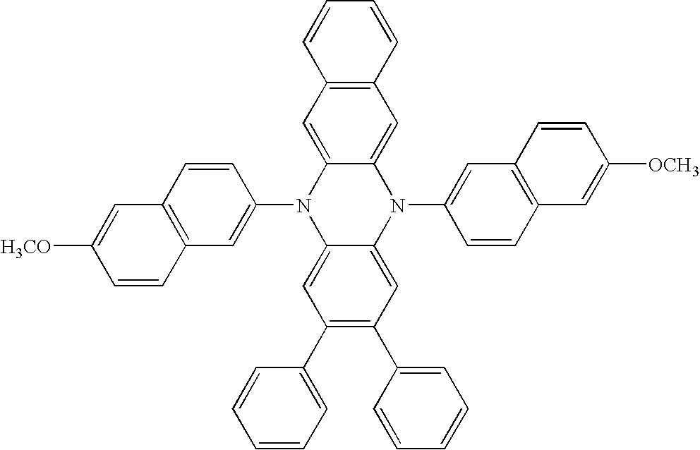
(XLVIII) 
(XLIX) 
(L) 
(LI) 
(LII) 
(LIII) 
(LIV) 
(LV) 
(LVI) 
(LVII) 
(LVIII) 
(LIX) 
(LX) 
(LXI) 
(LXII) 
(LXIII) 
(LXIV) 
(LXV) 
(LXVI) 
(LXVII) 
(LXVIII) 
(LXIX) 
(LXX) 
(LXXI) 
(LXXII) 
(LXXIII) 
(LXXIV) 
(LXXV) 
(LXXVI) 
(LXXVII) 
(LXXVIII) 
(LXXIX) 
(LXXX) 
(LXXXI) 
(LXXXII) 
(LXXXIII) 
(LXXXIV) 
(LXXXV) 
(LXXXVI) 
(LXXXVII) 
(LXXXVIII) 
(LXXXIX) 
(XC) 
(XCI) 
(XCII)
General Device Architecture - The present invention can be employed in most OLED device configurations. These include very simple structures comprising a single anode and cathode to more complex devices, such as passive matrix displays comprised of orthogonal arrays of anodes and cathodes to form pixels, and active-matrix displays where each pixel is controlled independently, for example, with a thin film transistor (TFT). The total combined thickness of the organic layers is preferably less than 500 nm.
- There are numerous configurations of the organic layers wherein the present invention can be successfully practiced. The compound of Formula 1 can be used wherever a hole transport material is called for. A typical structure is shown in
FIG. 1 and is comprised of asubstrate 101, an anode layer 103, an optional hole-injecting layer (HIL) 105, a hole-transporting layer (HTL) 107, a light-emitting layer (LEL) 109, an electron-transporting layer (ETL) 111, and acathode layer 113. These layers are described in detail below.FIG. 2 shows a variation of this embodiment in which there are employed two hole-transporting sublayers, 107 a and 107 b. - Substrate
- The
substrate 101 can either be light transmissive or opaque, depending on the intended direction of light emission. The light transmissive property is desirable for viewing the EL emission through the substrate. The transparent substrate may contain, or have built up on it, various electronic structures or circuitry (e.g., low temperature poly-silicon TFT structures) so long as a transparent region or regions remain. Transparent glass or plastic is commonly employed in such cases. For applications where the EL emission is viewed through the top electrode, the transmissive characteristic of the bottom support is immaterial, and therefore can be light transmissive, light absorbing or light reflective. Substrates for use in this case include, but are not limited to, glass, plastic, semiconductor materials, ceramics, and circuit board materials. Of course, it is necessary to provide in these device configurations a light transparent top electrode. The substrate, in some cases, may actually constitute the anode or cathode. - Anode
- The conductive anode layer 103 is formed over the substrate and, when EL emission is viewed through the anode, should be transparent or substantially transparent to the emission of interest. Common transparent anode materials used in this invention are indium-tin oxide and tin oxide, but other metal oxides can work including, but not limited to, aluminum- or indium-doped zinc oxide, magnesium-indium oxide, and nickel-tungsten oxide. In addition to these oxides, metal nitrides, such as gallium nitride, and metal selenides, such as zinc selenide, and metal sulfides, such as zinc sulfide, can be used in layer 103. For applications where EL emission is viewed through the top electrode, the transmissive characteristics of layer 103are immaterial and any conductive material can be used, transparent, opaque or reflective. Example conductors for this application include, but are not limited to, gold, iridium, molybdenum, palladium, and platinum. Typical anode materials, transmissive or otherwise, have a work function of 4.1 eV or greater. Desired anode materials are commonly deposited by any suitable means such as evaporation, sputtering, chemical vapor deposition, or electrochemical means. Anodes can be patterned using well-known photolithographic processes.
- Hole-Injecting Layer (HIL)
- While not always necessary, it is often useful that a hole-injecting
layer 105 be provided adjacent to the anode 103 and between the anode and the hole-transportinglayer 107. The hole-injecting material can serve to improve the film formation property of subsequent organic layers and to facilitate injection of holes into the hole-transporting layer. Suitable materials for use in the hole-injecting layer include, but are not limited to, porphyrinic compounds as described in U.S. Pat. No. 4,720,432, and plasma-deposited fluorocarbon polymers (CFx) as described in U.S. Pat. No. 6,208,075, and some aromatic amines, for example, m-MTDATA (4,4′,4″-tris[(3-methylphenyl)phenylamino]triphenylamine). Alternative hole-injecting materials reportedly useful in organic EL devices are described in EP 0 891 121 A1 and EP 1,029,909 A1. It is possible to employ materials useful in the invention in addition to the foregoing materials. - Hole-Transporting Layer (HTL)
- In a desirable embodiment of this invention, the hole-transporting layer 107 (or layers 107 a and 107 b) of the organic EL device contains at least one compound described in Formula 1. While the dihydrophenzine compound of Formula 1 can be used alone as the HTL material, a useful embodiment is to use two HTL materials preferably where the
layer 107 is divided into two regions or sublayers, 107 a and 107 b, as shown inFIG. 2 . The dihydrophenazine compound of Formula (1) can be used in either or both layers, but it is preferred if it is at least used in layer 107 a, closer to the anode. - Other HTL materials described below can be used in combination with Formula (1) as a mixture in
layer 107, or as a discrete material or mixture inlayers 107 a or 107 b. One useful class of hole-transporting compounds are aromatic tertiary amines, where the latter is understood to be a compound containing at least one trivalent nitrogen atom that is bonded only to carbon atoms, at least one of which is a member of an aromatic ring. In one form the aromatic tertiary amine can be an arylamine, such as a monoarylamine, diarylamine, triarylamine, or a polymeric arylamine. Exemplary monomeric triarylamines are illustrated by Klupfel et al. U.S. Pat. No. 3,180,730. Other suitable triarylamines substituted with one or more vinyl radicals and/or comprising at least one active hydrogen containing group are disclosed by Brantley et al. U.S. Pat. No. 3,567,450 and U.S. Pat. No. 3,658,520. - A more preferred class of aromatic tertiary amines are those which include at least two aromatic tertiary amine moieties as described in U.S. Pat. Nos. 4,720,432 and 5,061,569. Such compounds include those represented by structural Formula C.

wherein: - Q1 and Q2 are independently selected aromatic tertiary amine moieties; and
- G is a linking group such as an arylene, cycloalkylene, or alkylene group of a carbon to carbon bond.
In one embodiment, at least one of Q1 or Q2 contains a polycyclic fused ring structure, e.g., a naphthalene. When G is an aryl group, it is conveniently a phenylene, biphenylene, or naphthalene moiety. - A useful class of triarylamines satisfying structural Formula C and containing two triarylamine moieties is represented by structural Formula D:

wherein: - R1 and R2 each independently represents a hydrogen atom, an aryl group, or an alkyl group or R1 and R2 together represent the atoms completing a cycloalkyl group; and
- R3 and R4 each independently represents an aryl group, which is in turn substituted with a diaryl substituted amino group, as indicated by structural Formula E:

wherein - R5 and R6 are independently selected aryl groups. In one embodiment, at least one of R5 or R6 contains a polycyclic fused ring structure, e.g., a naphthalene.
- Another class of aromatic tertiary amines are the tetraaryldiamines. Desirable tetraaryldiamines include two diarylamino groups, such as indicated by Formula E, linked through an arylene group. Useful tetraaryldiamines include those represented by Formula F:

wherein: - each Are is an independently selected arylene group, such as a phenylene or anthracene moiety;
- n is an integer of from 1 to 4; and
- Ar, R7, R8, and R9 are independently selected aryl groups.
In a typical embodiment, at least one of Ar, R7, R8, and R9 is a polycyclic fused ring structure, e.g., a naphthalene - The various alkyl, alkylene, aryl, and arylene moieties of the foregoing structural Formulae C, D, E, F, can each in turn be substituted. Typical substituents include alkyl groups, alkoxy groups, aryl groups, aryloxy groups, and halogen such as fluoride, chloride, and bromide. The various alkyl and alkylene moieties typically contain from about 1 to 6 carbon atoms. The cycloalkyl moieties can contain from 3 to about 10 carbon atoms, but typically contain five, six, or seven ring carbon atoms—e.g., cyclopentyl, cyclohexyl, and cycloheptyl ring structures. The aryl and arylene moieties are usually phenyl and phenylene moieties.
- Illustrative of useful aromatic tertiary amines are the following:
- 1,1-Bis(4-di-p-tolylaminophenyl)cyclohexane
- 1,1-Bis(4-di-p-tolylaminophenyl)-4-phenylcyclohexane
- 4,4′-Bis(diphenylamino)quadriphenyl
- Bis(4-dimethylamino-2-methylphenyl)-phenylmethane
- N,N,N-Tri(p-tolyl)amine
- 4-(di-p-tolylamino)-4′-[4(di-p-tolylamino)-styryl]stilbene
- N,N,N′,N′-Tetra-p-tolyl-4-4′-diaminobiphenyl
- N,N,N′,N′-Tetraphenyl-4,4′-diaminobiphenyl
- N-Phenylcarbazole
- Poly(N-vinylcarbazole), and
- N,N′-di-1-naphthalenyl-N,N′-diphenyl-4,4′-diaminobiphenyl.
- 4,4′-Bis[N-(1-naphthyl)-N-phenylamino]biphenyl
- 4,4″-Bis[N-(1-naphthyl)-N-phenylamino]p-terphenyl
- 4,4′-Bis[N-(2-naphthyl)-N-phenylamino]biphenyl “NPB”
- 4,4′-Bis[N-(3-acenaphthenyl)-N-phenylamino]biphenyl
- 1,5-Bis[N-(1-naphthyl)-N-phenylamino]naphthalene
- 4,4′-Bis[N-(9-anthryl)-N-phenylamino]biphenyl
- 4,4″-Bis[N-(1-anthryl)-N-phenylamino]-p-terphenyl
- 4,4′-Bis[N-(2-phenanthryl)-N-phenylamino]biphenyl
- 4,4′-Bis[N-(8-fluoranthenyl)-N-phenylamino]biphenyl
- 4,4′-Bis[N-(2-pyrenyl)-N-phenylamino]biphenyl
- 4,4′-Bis[N-(2-naphthacenyl)-N-phenylamino]biphenyl
- 4,4′-Bis[N-(2-perylenyl)-N-phenylamino]biphenyl
- 4,4′-Bis[N-(1-coronenyl)-N-phenylamino]biphenyl
- 2,6-Bis(di-p-tolylamino)naphthalene
- 2,6-Bis[di-(1-naphthyl)amino]naphthalene
- 2,6-Bis[N-(1-naphthyl)-N-(2-naphthyl)amino]naphthalene
- N,N,N′,N′-Tetra(2-naphthyl)-4,4″-diamino-p-terphenyl
- 4,4′-Bis {N-phenyl-N-[4-(1-naphthyl)-phenyl]amino}biphenyl
- 4,4′-Bis[N-phenyl-N-(2-pyrenyl)amino]biphenyl
- 2,6-Bis[N,N-di(2-naphthyl)amine]fluorene
- 1,5-Bis[N-(1-naphthyl)-N-phenylamino]naphthalene
- N,N′-di-1-naphthalenyl-N,N′-di-2-naphthalenyl-[1,1′-biphenyl]-4,4′-diamine.
Light-Emitting Layer (LEL) - As more fully described in U.S. Pat. Nos. 4,769,292 and 5,935,721, the light-emitting
layer 109 of the organic EL element comprises a luminescent or fluorescent material where electroluminescence is produced as a result of electron-hole pair recombination in this region. The light-emitting layer can be comprised of a single material, but more commonly consists of a host material doped with a guest compound or compounds where light emission comes primarily from the dopant and can be of any color. The host materials in the light-emitting layer can be an electron-transporting material, as defined below, a hole-transporting material, as defined above, a mixture of hole- and electron-transporting materials, or another material or mixture that supports hole-electron recombination. The dopant is usually chosen from highly fluorescent dyes, but phosphorescent compounds, e.g., transition metal complexes as described in WO 98/55561, WO 00/18851, WO 00/57676, and WO 00/70655 are also useful. Dopants are typically coated as 0.01 to 10% by weight into the host material. - An important relationship for choosing a dye as a dopant is a comparison of the bandgap potential which is defined as the energy difference between the highest occupied molecular orbital and the lowest unoccupied molecular orbital of the molecule. For efficient energy transfer from the host to the dopant molecule, a necessary condition is that the band gap of the dopant is smaller than that of the host material.
- Host and emitting molecules known to be of use include, but are not limited to, those disclosed in U.S. Pat. Nos. 4,768,292; 5,141,671; 5,150,006; 5,151,629; 5,405,709; 5,484,922; 5,593,788; 5,645,948; 5,683,823; 5,755,999; 5,928,802; 5,935,720; 5,935,721; and 6,020,078.
- Metal complexes of 8-hydroxyquinoline and similar derivatives (Formula G) constitute one class of useful host compounds capable of supporting electroluminescence, and are particularly suitable for light emission of wavelengths longer than 500 nm, e.g., green, yellow, orange, and red.

wherein: - M represents a metal;
- n is an integer of from 1 to 3; and
- Z independently in each occurrence represents the atoms completing a nucleus having at least two fused aromatic rings.
- From the foregoing it is apparent that the metal can be monovalent, divalent, or trivalent metal. The metal can, for example, be an alkali metal, such as lithium, sodium, or potassium; an alkaline earth metal, such as magnesium or calcium; or an earth metal, such as boron or aluminum. Generally any monovalent, divalent, or trivalent metal known to be a useful chelating metal can be employed.
- Z completes a heterocyclic nucleus containing at least two fused aromatic rings, at least one of which is an azole or azine ring. Additional rings, including both aliphatic and aromatic rings, can be fused with the two required rings, if required. To avoid adding molecular bulk without improving on function the number of ring atoms is usually maintained at 18 or less.
- Illustrative of useful chelated oxinoid compounds are the following:
- CO-1: Aluminum trisoxine [alias, tris(8-quinolinolato)aluminum(III)]
- CO-2: Magnesium bisoxine [alias, bis(8-quinolinolato)magnesium(II)]
- CO-3: Bis[benzo{f}-8-quinolinolato]zinc (II)
- CO-4: Bis(2-methyl-8-quinolinolato)aluminum(III)-μ-oxo-bis(2-methyl-8-quinolinolato) aluminum(III)
- CO-5: Indium trisoxine [alias, tris(8-quinolinolato)indium]
- CO-6: Aluminum tris(5-methyloxine) [alias, tris(5-methyl-8-quinolinolato) aluminum(III)]
- CO-7: Lithum oxine [alias, (8-quinolinolato)lithium(I)]
- Derivatives of 9,10-di-(2-naphthyl)anthracene (Formula H) constitute one class of useful hosts capable of supporting electroluminescence, and are particularly suitable for light emission of wavelengths longer than 400 nm, e.g., blue, green, yellow, orange or red.

wherein R1, R2, R3, R4, R5, and R6 represent one or more substituents on each ring where each substituent is individually selected from the following groups: - Group 1: hydrogen, or alkyl of from 1 to 24 carbon atoms;
- Group 2: aryl or substituted aryl of from 5 to 20 carbon atoms;
- Group 3: carbon atoms from 4 to 24 necessary to complete a fused aromatic ring of anthracenyl; pyrenyl, or perylenyl;
- Group 4: heteroaryl or substituted heteroaryl of from 5 to 24 carbon atoms as necessary to complete a fused heteroaromatic ring of furyl, thienyl, pyridyl, quinolinyl or other heterocyclic systems;
- Group 5:alkoxylamino, alkylamino, or arylamino of from 1 to 24 carbon atoms; and
- Group 6:fluorine, chlorine, bromine or cyano.
- Benzazole derivatives (Formula I) constitute another class of useful hosts capable of supporting electroluminescence, and are particularly suitable for light emission of wavelengths longer than 400 nm, e.g., blue, green, yellow, orange or red.

where: - N is an integer of 3 to 8;
- Z is O, NR or S; and
- R and R′ are individually hydrogen; alkyl of from 1 to 24 carbon atoms, for example, propyl, t-butyl, heptyl, and the like; aryl or hetero-atom substituted aryl of from 5 to 20 carbon atoms for example phenyl and naphthyl, furyl, thienyl, pyridyl, quinolinyl and other heterocyclic systems; or halo such as chloro, fluoro; or atoms necessary to complete a fused aromatic ring;
- B is a linkage unit consisting of alkyl, aryl, substituted alkyl, or substituted aryl, which conjugately or unconjugately connects the multiple benzazoles together.
- An example of a useful benzazole is 2,2′,2″-(1,3,5-phenylene)tris[1-phenyl-1H-benzimidazole].
- Desirable fluorescent dopants include derivatives of anthracene, tetracene, xanthene, perylene, rubrene, coumarin, rhodamine, quinacridone, dicyanomethylenepyran compounds, thiopyran compounds, polymethine compounds, pyrilium and thiapyrilium compounds, and carbostyryl compounds. Illustrative examples of useful luminescent dopants include, but are not limited to, the following:


Electron-Transporting Layer (ETL) - Preferred thin film-forming materials for use in forming the electron-transporting
layer 111 of the organic EL devices of this invention are metal chelated oxinoid compounds, including chelates of oxine itself (also commonly referred to as 8-quinolinol or 8-hydroxyquinoline). Such compounds help to inject and transport electrons and exhibit both high levels of performance and are readily fabricated in the form of thin films. Exemplary of contemplated oxinoid compounds are those satisfying structural Formula G, previously described. - Other electron-transporting materials include various butadiene derivatives as disclosed in U.S. Pat. No. 4,356,429 and various heterocyclic optical brighteners as described in U.S. Pat. No. 4,539,507. Benzazoles satisfying structural Formula I are also useful electron transporting materials.
- In some instances,
layers - Cathode
- When light emission is through the anode, the
cathode layer 113 used in this invention can be comprised of nearly any conductive material. Desirable materials have good film-forming properties to ensure good contact with the underlying organic layer, promote electron injection at low voltage, and have good stability. Useful cathode materials often contain a low work function metal (<4.0 eV) or metal alloy. One preferred cathode material is comprised of a Mg:Ag alloy wherein the percentage of silver is in the range of 1 to 20%, as described in U.S. Pat. No. 4,885,221. Another suitable class of cathode materials includes bilayers comprised of a thin layer of a low work function metal or metal salt capped with a thicker layer of conductive metal. One such cathode is comprised of a thin layer of LiF followed by a thicker layer of Al as described in U.S. Pat. No. 5,677,572. Other useful cathode materials include, but are not limited to, those disclosed in U.S. Pat. Nos. 5,059,861; 5,059,862; and 6,140,763. - When light emission is viewed through the cathode, the cathode must be transparent or nearly transparent. For such applications, metals must be thin or one must use transparent conductive oxides, or a combination of these materials. Optically transparent cathodes have been described in more detail in U.S. Pat. No. 5,776,623. Cathode materials can be deposited by evaporation, sputtering, or chemical vapor deposition. When needed, patterning can be achieved through many well known methods including, but not limited to, through-mask deposition, integral shadow masking as described in U.S. Pat. No. 5,276,380 and EP 0 732 868, laser ablation, and selective chemical vapor deposition.
- Deposition of Organic Layers
- The organic materials mentioned above are suitably deposited through a vapor-phase method such as thermal evaporation, but can be deposited from a fluid, for example, from a solvent with an optional binder to improve film formation. If the material is a polymer, solvent deposition is useful but other methods can be used, such as sputtering or thermal transfer from a donor sheet. The material to be deposited by thermal evaporation can be vaporized from an evaporation “boat” often comprised of a tantalum material, e.g., as described in U.S. Pat. No. 6,237,529, or can be first coated onto a donor sheet and then sublimed in closer proximity to the substrate. Layers with a mixture of materials can utilize separate evaporation boats or the materials can be pre-mixed and coated from a single boat or donor sheet. Patterned deposition can be achieved using shadow masks, integral shadow masks (U.S. Pat. No. 5,294,870), spatially-defined thermal dye transfer from a donor sheet (U.S. Pat. Nos. 5,688,551; 5,851,709; and 6,066,357) and inkjet method (U.S. Pat. No. 6,066,357).
- Encapsulation
- Most OLED devices are sensitive to moisture and/or oxygen so they are commonly sealed in an inert atmosphere such as nitrogen or argon, along with a desiccant such as alumina, bauxite, calcium sulfate, clays, silica gel, zeolites, alkaline metal oxides, alkaline earth metal oxides, sulfates, or metal halides and perchlorates. Methods for encapsulation and desiccation include, but are not limited to, those described in U.S. Pat. No. 6,226,890.
- The entire contents of the patents and other publications referred to in this specification are incorporated herein by reference.
- Synthesis of Dihydrophenazine Compounds
- Dihydrophenazine compounds can be synthesized in two steps. Step one involves a condensation reaction between an aryl dihydroxy derivative and an aryl diamino derivative to produce a dihydrophenazine intermediate. These intermediates, which are prone to oxidation if proper precaution is not taken, are then N-alkylated or N-arylated using well known Pd catalyzed cross coupling chemistry.
- The synthesis of compounds I-IV is illustrated in the synthetic scheme. Compounds I-IV are then reacted with the appropriate aryl bromide to yield compounds V-XVII.

Synthesis of 5,10-dihydrophenazine (I) - Synthesized according to Mikulla, Markus; Mulhaupt, Rolf, Macromol. Chem. Phys., 199, 795-805, (1998).
- Synthesis of 5,12-dihydro-benzo[b]phenazine (II)
- 2,3-dihydroxynapthalene (10 g, 62.5 mmol), 1,2-phenylenediamine (6.75 g, 62.5 mmol) and N,N-dimethylaniline (54 ml) are placed into a round bottom flask under nitrogen atmosphere. Mixture is stirred at reflux. Reaction is monitored by TLC (CH2Cl2:Heptane/1:1) until all 2,3-dihydroxynaphthalene has reacted (˜3 hours). After cooling to room temperature, toluene (100 ml) is added and solid is collected by vacuum filtration. After washing with toluene (50 ml), ethanol (100 ml) and hexanes (50 ml), the product is dried under vacuum to yield 11.0 g (76% yield) of light yellow solid.
- Synthesis of 5,12-dihydro-2,3-dimethyl-benzo[b]phenazine (III)
- 2,3-dihydroxynapthalene (10 g, 62.5 mmol), 4,5-dimethyl-1,2-phenylenediamine (8.5 g, 62.5 mmol) and N,N-dimethylaniline (54 ml) are placed into a round bottom flask under nitrogen atmosphere. Mixture is stirred at reflux. Reaction is monitored by TLC (CH2Cl2:Heptane/1:1) until all 2,3-dihydroxynaphthalene has reacted (˜3 hours). After cooling to room temperature, toluene (100 ml) is added and solid is collected by vacuum filtration. After washing with toluene (50 ml), ethanol (100 ml) and hexanes (50 ml), the product is dried under vacuum to yield 23.3 g (33% yield) of light yellow solid.
- Synthesis of 6,13-dihydro-dibenzo[b,i]phenazine (IV)
- 2,3-dihydroxynapthalene (10 g, 62.5 mmol), 2,3-diaminonaphthalene (9.9 g, 62.5 mmol) and N,N-dimethylaniline (54 ml) are placed into a round bottom flask under nitrogen atmosphere. Mixture is stirred at reflux. Reaction is monitored by TLC (CH2Cl2:Heptane/1:1) until all 2,3-dihydroxynaphthalene has reacted (˜3 hours). After cooling to room temperature, toluene (100 ml) is added and solid is collected by vacuum filtration. After washing with toluene (50 ml), ethanol (100 ml) and hexanes (50 ml), the product is dried under vacuum to yield 11.5 g (65% yield) of light yellow solid.
- Procedure for the Pd Catalyzed Cross Coupling Reaction of Dihydrophenazines (I-IV) with Aryl Bromides
- Dihdyrophenazine compound, (1 equivalent), aryl bromide (2.2 equivalents), sodium tert-butoxide (3.0 equivalents), [Pd2(dba)3] tris(dibenzylideneacetone)dipalladium(0) (3 mol % of dihydrophenazine compound), tri-tert-butylphosphine (0.8 equivalents of Pd catalyst), and sodium tert-butoxide (3 equivalents) were all placed into a round bottom flask under a nitrogen atmosphere. Anhydrous toluene is added using a cannula and mixture is heated at reflux overnight. Two workup procedures were used depending on the solubility of the product in toluene.
- Workup Procedure 1 (product not soluble in toluene): Upon cooling the reaction to room temperature, the precipitated solid is collected by vacuum filtration and washed with additional toluene. The filter cake is then washed extensively with water, followed by ethanol, cold tetrahydrofuran and lastly, hexanes. The product is then dried in an oven to give pure material.
- Workup Procedure 2 (product is soluble in toluene): Reaction mixture is filtered while hot and the filter is washed with additional toluene. The filtrate is concentrated to a dark solid. After dissolving in CH2Cl2 and passing through a pad of silica gel, solvent is removed by rotary evaporation. Hexane is added and product is collected by filtration and dried in an oven to give pure material.
- After products are collected by filtration and dried thoroughly, all materials are sublimed by train sublimation at 600 mTorr.
- The invention and its advantages are further illustrated by the specific examples which follow.
- The above general procedure was followed using compound (II) [3.0 g, 12.9 mmol], 4-bromotoluene [4.86 g, 28.5 mmol], sodium tert-butoxide [3.2 g, 33.3 mmol], Pd2(dba)3 [300 mg, 0.32 mmol], few drops tri-tert-butylphosphine and 50 ml toluene. Workup procedure 2 was used which gave 3.1 g (58% yield) of (VI) as a brown solid after sublimation. Proton NMR was consistent with the product. FD-MS (m/z): 412.
- In an Ace pressure bottle equipped with stirbar under an atmosphere of argon, were combined 5 g (19.2 mmol) of 5,12-dihydro-2,3-dimethyl-benzo(b)phenazine, 0.36 g of tris(dibenzylideneacetone)-dipalladium(0), dry degassed toluene (40 mL), 4-bromotoluene (5.2 mL, 42 mmol), tri(t-butyl)phoshine (0.96 mL of a 0.33 M solution in hexane), and finally 5.54 g of sodium t-butoxide (57.6 mmol). The bottle was sealed and heated at 125° C. (external temperature) for 12 h. The resultant reaction mixture was cooled, diluted with dichloromethane, and passed through a pad of silica gel. The eluent was concentrated and the process repeated to provide 7.95 g (94% yield) of (IX). Proton NMR was consistent with the product. ES-MS(m/z): 440
- The above general procedure was followed using compound (III) [3.0 g, 11.5 mmol], 2-bromonaphthalene [4.95 g, 23.0 mmol], sodium tert-butoxide [3.4 g, 35.4 mmol), Pd2(dba)3 [300 mg, 0.32 mmol], few drops tri-tert-butylphosphine and 50 ml toluene. Workup procedure 1 was used which gave 4.0 g (68% yield) of (X) as a yellow solid after sublimation. Proton NMR was consistent with the product. FD-MS (m/z): 512.
- The above general procedure was followed using compound (III) [3.0 g, 11.5 mmol], 2-bromo-6-methoxynaphthalene [5.5 g, 23.2 mmol], sodium tert-butoxide [3.4 g, 35.4 mmol), Pd2(dba)3 [300 mg, 0.32 mmol], few drops tri-tert-butylphosphine and 75 ml toluene. Workup procedure 1 was used which gave 4.0 g (61% yield) of (XI) as a yellow solid after sublimation. Proton NMR was consistent with the product. FD-MS (m/z): 572.
- The above general procedure was followed using compound (III) [3.0 g, 11.5 mmol], 4-bromo-1,1′-biphenyl [5.4 g, 23.1 mmol], sodium tert-butoxide [3.4 g, 35.4 mmol), Pd2(dba)3 [300 mg, 0.32 mmol], few drops tri-tert-butylphosphine and 75 ml toluene. Workup procedure 1 was used which gave 5.6 g (86% yield) of (XII) as a yellow solid after sublimation. Proton NMR was consistent with the product. FD-MS (m/z): 564.
- The above general procedure was followed using compound (IV) [3.0 g, 10.6 mmol], 1-bromo-4-methyl-benzene [4.0 g, 23.4 mmol], sodium tert-butoxide [3.2 g, 33.3 mmol), Pd2(dba)3 [300 mg, 0.32 mmol], few drops tri-tert-butylphosphine and 75 ml toluene. Workup procedure 1 was used which gave 3.2 g (65% yield) of (XIII) as a yellow solid after sublimation. Proton NMR was consistent with the product. FD-MS (m/z): 462.
- The above general procedure was followed using compound (IV) [2.6 g, 9.2 mmol], 2-bromonaphthalene [4.0 g, 19.3 mmol], sodium tert-butoxide [3.0 g, 31.2 mmol), Pd2(dba)3 [300 mg, 0.32 mmol], few drops tri-tert-butylphosphine and 60 ml toluene. Workup procedure 1 was used which gave 4.8 g (97% yield) of (XIV) as a yellow solid after sublimation. Proton NMR was consistent with the product. FD-MS (m/z): 534.
- The above general procedure was followed using compound (IV) [3.0 g, 10.6 mmol], 2-bromo-6-methoxynaphthalene [5.55 g, 23.4 mmol], sodium tert-butoxide [3.2 g, 33.3 mmol), Pd2(dba)3 [300 mg, 0.32 mmol], few drops tri-tert-butylphosphine and 60 ml toluene. Workup procedure 1 was used which gave 4.0 g (63% yield) of (XV) as a yellow solid after sublimation. Proton NMR was consistent with the product. FD-MS (m/z): 594.
- The invention and its advantages are further illustrated by the specific examples which follow.
- EL devices satisfying the requirements of the invention were constructed in the following manner:
- A˜1.1 mm thick glass substrate coated with a transparent ITO conductive layer was cleaned and dried using a commercial glass scrubber tool. The thickness of ITO is about 42 nm and the sheet resistance of the ITO is about 68Ω/square. The ITO surface was subsequently treated with oxidative plasma to condition the surface as an anode. A layer of CFx, 1 nm thick, was deposited on the clean ITO surface by decomposing CHF3 gas in an RF plasma treatment chamber. The substrate was then transferred into a vacuum deposition chamber for deposition of all other layers on top of the substrate. The following layers were deposited in the following sequence by sublimation from a heated boat under a vacuum of approximately 10−6 Torr:
- a) a layer of Compound VI (see Table 2 for layer thickness);
- b) a hole-transporting layer of N,N′-di(1-naphthyl)-N,N′-diphenyl-4,4′-diaminobiphenyl (NPB, see Table 2 for layer thickness);
- c) a 37.5 nm light-emitting layer of tris(8-quinolinolato)aluminum (III) (AlQ3);
- d) a 37.5 nm electron transport layer of AlQ3; and
- e) a 210 nm cathode formed of a 10:0.5 atomic ratio of Mg and Ag.
After the deposition of these layers, the device was transferred from the deposition chamber into a dry box for encapsulation. - Devices were prepared as the same as device examples 1-1 and 1-2 except that compound VI was replaced with compound IX.
- Devices were prepared as the same as device examples 1-1 and 1-2 except that compound VI was replaced with compound X.
- Devices were prepared as the same as device examples 1-1 and 1-2 except that compound VI was replaced with compound XI.
- Devices were prepared as the same as device examples 1-1 and 1-2 except that compound VI was replaced with compound XII.
- Devices were prepared as the same as device examples 1-1 and 1-2 except that compound VI was replaced with compound XIII.
- Devices were prepared as the same as device examples 1-1 and 1-2 except that compound VI was replaced with compound XIV.
- Devices were prepared as the same as device examples 1-1 and 1-2 except that compound VI was replaced with compound XV.
- A device was prepared as the same as device examples 1-1 and 1-2 except that layer (a) was omitted and the device contained an overall hole-transporting layer thickness substantially the same as the other examples.
- The cells thus formed were tested for luminance with a constant current of 20 mA/cm2 and the results are reported in Table 2. It can be seen from Table 2 that the compounds useful in the invention, when incorporated into EL cells, give an increase in luminance of 44-99% compared to the comparative device examples.
TABLE 2 Evaluation Results for Device Examples 1-9 Device Layer (a) Layer (b) Cell Relative Ex- Thickness Thickness Luminance Lumi- ample Type (nm) (nm) (candela/m2) nance (%) 9-1 Comparative 0.0 75.0 525 100 8-1 Inventive 55.1 20.0 821 156 8-2 Inventive 75.1 0.0 265 50 7-1 Inventive 55.2 20.3 1023 195 7-2 Inventive 70.1 5.3 976 186 6-1 Inventive 55.0 20.1 906 173 6-2 Inventive 75.0 0.0 329 63 5-1 Inventive 5.3 70.3 1043 199 5-2 Inventive 20.1 55.0 834 159 4-1 Inventive 55.1 20.0 871 166 4-2 Inventive 70.2 5.2 834 159 3-1 Inventive 20.1 55.3 946 180 3-2 Inventive 55.0 20.1 986 188 2-1 Inventive 5.0 70.1 1027 196 2-2 Inventive 55.0 20.0 1013 193 1-1 Inventive 5.0 70.0 757 144 1-2 Inventive 55.1 20.1 893 170 - It is noted that Device Examples 8-2 and 6-2 provide useful luminance although not as good as the previously known NPB compound. Moreover, when dihydrophenazine compounds are used in combination with the NPB compound, superior results are obtained compared to the use of NPB or the dihydrophenazine compound alone.
- A series of EL devices were prepared as described in device examples 1-1 and 1-2. Compound VI was replaced with compound X and a green fluorescent dopant, 5,12-dihydro-5,12-diphenyl-quino[2,3-b]acridine-7,14-dione (DPQA), was co-deposited in the AlQ3 light emitting layer (c) at a level of 0.6%.

- A device was prepared as the same as device examples 10-1, 10-2 and 10-3 except that layer (a) was omitted and the device contained an overall hole-transporting layer thickness substantially the same as the other examples.
- The cells thus formed were tested for luminance with a constant current of 20 mA/cm2 and the results are reported in Table 3. It can be seen from Table 3 that the compounds useful in the invention, when incorporated into green doped EL cells, give an increase in luminance of 20-36% compared to the comparative device example. In addition, the EL color of the cells was green with average 1931 CIE color coordinates of x=0.315 and y=0.650. The EL spectra indicate that the green EL emission originates from the dopant in the Alq3 layer. Cells containing the dihydrophenazine compound gave improved luminance.
TABLE 3 Evaluation Results for Device Examples 10-11 Device Layer (a) Layer (b) Cell Relative Ex- Thickness Thickness Luminance Lumi- ample Type (nm) (nm) (candela/m2) nance (%) 11-1 Comparative 0.0 75.0 1756 100 10-1 Inventive 5.3 70.0 2300 131 10-2 Inventive 55.1 20.2 2392 136 10-3 Inventive 70.0 50.0 2103 120 - The invention has been described in detail with particular reference to certain preferred embodiments thereof, but it will be understood that variations and modifications can be effected within the spirit and scope of the invention.
-
- 101 substrate
- 103 anode
- 105 hole-injecting layer (HIL)
- 107 hole-transporting layer (HTL)
- 107 a hole-transporting sublayer closer to anode
- 107 b hole-transporting sublayer further from anode.
- 109 light-emitting layer (LEL)
- 111 electron-transporting layer (ETL)
- 113 cathode
Claims (48)


Priority Applications (1)
| Application Number | Priority Date | Filing Date | Title |
|---|---|---|---|
| US10/617,319 US6919140B2 (en) | 2003-07-10 | 2003-07-10 | Organic electroluminescent devices with high luminance |
Applications Claiming Priority (1)
| Application Number | Priority Date | Filing Date | Title |
|---|---|---|---|
| US10/617,319 US6919140B2 (en) | 2003-07-10 | 2003-07-10 | Organic electroluminescent devices with high luminance |
Publications (2)
| Publication Number | Publication Date |
|---|---|
| US20050014018A1 true US20050014018A1 (en) | 2005-01-20 |
| US6919140B2 US6919140B2 (en) | 2005-07-19 |
Family
ID=34062396
Family Applications (1)
| Application Number | Title | Priority Date | Filing Date |
|---|---|---|---|
| US10/617,319 Expired - Lifetime US6919140B2 (en) | 2003-07-10 | 2003-07-10 | Organic electroluminescent devices with high luminance |
Country Status (1)
| Country | Link |
|---|---|
| US (1) | US6919140B2 (en) |
Cited By (13)
| Publication number | Priority date | Publication date | Assignee | Title |
|---|---|---|---|---|
| WO2007015412A1 (en) * | 2005-08-03 | 2007-02-08 | Nippon Steel Chemical Co., Ltd. | Heterocyclic compound and organic electroluminescent device using same |
| US20070126347A1 (en) * | 2005-12-01 | 2007-06-07 | Eastman Kodak Company | OLEDS with improved efficiency |
| US20080079356A1 (en) * | 2006-09-29 | 2008-04-03 | Sang-Hoon Park | Organoelectroluminescent compound and organoelectroluminescent device employing the same |
| US20090115329A1 (en) * | 2003-08-14 | 2009-05-07 | Lg Electronics Inc. | Organic el device |
| EP2100941A3 (en) * | 2008-03-14 | 2010-10-06 | Gracel Display Inc. | Novel organic electroluminescent compounds and organic electroluminescent device using the same |
| WO2011052285A1 (en) * | 2009-10-28 | 2011-05-05 | シャープ株式会社 | Novel compound, field-effective transistor, solar cell, method for producing said compound, field-effective transistor, and solar cell, composition for organic semiconductor layer, and composition for p-type semiconductor layer |
| CN102491950A (en) * | 2011-12-09 | 2012-06-13 | 华东理工大学 | Quinoxaline derivative and preparation method thereof |
| CN103980254A (en) * | 2014-04-01 | 2014-08-13 | 上海道亦化工科技有限公司 | Organic electroluminescence compound |
| TWI548638B (en) * | 2013-09-30 | 2016-09-11 | Lg化學股份有限公司 | Heterocyclic compound and organic light emitting device using the same |
| CN110299460A (en) * | 2019-06-24 | 2019-10-01 | 武汉华星光电半导体显示技术有限公司 | A kind of hole mobile material, preparation method and electroluminescent device |
| CN110407817A (en) * | 2019-07-04 | 2019-11-05 | 武汉华星光电半导体显示技术有限公司 | Hole mobile material and preparation method thereof, electroluminescent device |
| CN112079786A (en) * | 2019-06-14 | 2020-12-15 | 北京鼎材科技有限公司 | Compound, organic electronic light-emitting device comprising compound and application of compound |
| US11355713B2 (en) * | 2019-06-24 | 2022-06-07 | Wuhan China Star Optoelectronics Semiconductor Display Technology Co., Ltd. | Hole transport material, manufacturing method thereof, and electroluminescent device thereof |
Citations (17)
| Publication number | Priority date | Publication date | Assignee | Title |
|---|---|---|---|---|
| US3172862A (en) * | 1960-09-29 | 1965-03-09 | Dow Chemical Co | Organic electroluminescent phosphors |
| US3173050A (en) * | 1962-09-19 | 1965-03-09 | Dow Chemical Co | Electroluminescent cell |
| US3710167A (en) * | 1970-07-02 | 1973-01-09 | Rca Corp | Organic electroluminescent cells having a tunnel injection cathode |
| US4356429A (en) * | 1980-07-17 | 1982-10-26 | Eastman Kodak Company | Organic electroluminescent cell |
| US4539507A (en) * | 1983-03-25 | 1985-09-03 | Eastman Kodak Company | Organic electroluminescent devices having improved power conversion efficiencies |
| US4720432A (en) * | 1987-02-11 | 1988-01-19 | Eastman Kodak Company | Electroluminescent device with organic luminescent medium |
| US4769292A (en) * | 1987-03-02 | 1988-09-06 | Eastman Kodak Company | Electroluminescent device with modified thin film luminescent zone |
| US5061569A (en) * | 1990-07-26 | 1991-10-29 | Eastman Kodak Company | Electroluminescent device with organic electroluminescent medium |
| US5409783A (en) * | 1994-02-24 | 1995-04-25 | Eastman Kodak Company | Red-emitting organic electroluminescent device |
| US5554450A (en) * | 1995-03-08 | 1996-09-10 | Eastman Kodak Company | Organic electroluminescent devices with high thermal stability |
| US5593788A (en) * | 1996-04-25 | 1997-01-14 | Eastman Kodak Company | Organic electroluminescent devices with high operational stability |
| US5683823A (en) * | 1996-01-26 | 1997-11-04 | Eastman Kodak Company | White light-emitting organic electroluminescent devices |
| US5908581A (en) * | 1997-04-07 | 1999-06-01 | Eastman Kodak Company | Red organic electroluminescent materials |
| US5928802A (en) * | 1997-05-16 | 1999-07-27 | Eastman Kodak Company | Efficient blue organic electroluminescent devices |
| US6020078A (en) * | 1998-12-18 | 2000-02-01 | Eastman Kodak Company | Green organic electroluminescent devices |
| US6208077B1 (en) * | 1998-11-05 | 2001-03-27 | Eastman Kodak Company | Organic electroluminescent device with a non-conductive fluorocarbon polymer layer |
| US20040004215A1 (en) * | 2002-05-31 | 2004-01-08 | Hiroyuki Iechi | Vertical organic transistor |
Family Cites Families (6)
| Publication number | Priority date | Publication date | Assignee | Title |
|---|---|---|---|---|
| JPS6143689A (en) * | 1984-08-07 | 1986-03-03 | Canon Inc | El element |
| US6344283B1 (en) | 1996-12-28 | 2002-02-05 | Tdk Corporation | Organic electroluminescent elements |
| JP3503403B2 (en) * | 1997-03-17 | 2004-03-08 | 東洋インキ製造株式会社 | Light emitting material for organic electroluminescent device and organic electroluminescent device using the same |
| JP3829008B2 (en) | 1998-03-19 | 2006-10-04 | 株式会社リコー | Temperature control apparatus and image forming apparatus having the same |
| JP2000021574A (en) * | 1998-06-29 | 2000-01-21 | Canon Inc | Light emitting element |
| JP2000260565A (en) * | 1999-03-04 | 2000-09-22 | Futaba Corp | Organic el element |
-
2003
- 2003-07-10 US US10/617,319 patent/US6919140B2/en not_active Expired - Lifetime
Patent Citations (17)
| Publication number | Priority date | Publication date | Assignee | Title |
|---|---|---|---|---|
| US3172862A (en) * | 1960-09-29 | 1965-03-09 | Dow Chemical Co | Organic electroluminescent phosphors |
| US3173050A (en) * | 1962-09-19 | 1965-03-09 | Dow Chemical Co | Electroluminescent cell |
| US3710167A (en) * | 1970-07-02 | 1973-01-09 | Rca Corp | Organic electroluminescent cells having a tunnel injection cathode |
| US4356429A (en) * | 1980-07-17 | 1982-10-26 | Eastman Kodak Company | Organic electroluminescent cell |
| US4539507A (en) * | 1983-03-25 | 1985-09-03 | Eastman Kodak Company | Organic electroluminescent devices having improved power conversion efficiencies |
| US4720432A (en) * | 1987-02-11 | 1988-01-19 | Eastman Kodak Company | Electroluminescent device with organic luminescent medium |
| US4769292A (en) * | 1987-03-02 | 1988-09-06 | Eastman Kodak Company | Electroluminescent device with modified thin film luminescent zone |
| US5061569A (en) * | 1990-07-26 | 1991-10-29 | Eastman Kodak Company | Electroluminescent device with organic electroluminescent medium |
| US5409783A (en) * | 1994-02-24 | 1995-04-25 | Eastman Kodak Company | Red-emitting organic electroluminescent device |
| US5554450A (en) * | 1995-03-08 | 1996-09-10 | Eastman Kodak Company | Organic electroluminescent devices with high thermal stability |
| US5683823A (en) * | 1996-01-26 | 1997-11-04 | Eastman Kodak Company | White light-emitting organic electroluminescent devices |
| US5593788A (en) * | 1996-04-25 | 1997-01-14 | Eastman Kodak Company | Organic electroluminescent devices with high operational stability |
| US5908581A (en) * | 1997-04-07 | 1999-06-01 | Eastman Kodak Company | Red organic electroluminescent materials |
| US5928802A (en) * | 1997-05-16 | 1999-07-27 | Eastman Kodak Company | Efficient blue organic electroluminescent devices |
| US6208077B1 (en) * | 1998-11-05 | 2001-03-27 | Eastman Kodak Company | Organic electroluminescent device with a non-conductive fluorocarbon polymer layer |
| US6020078A (en) * | 1998-12-18 | 2000-02-01 | Eastman Kodak Company | Green organic electroluminescent devices |
| US20040004215A1 (en) * | 2002-05-31 | 2004-01-08 | Hiroyuki Iechi | Vertical organic transistor |
Cited By (23)
| Publication number | Priority date | Publication date | Assignee | Title |
|---|---|---|---|---|
| US8512876B2 (en) * | 2003-08-14 | 2013-08-20 | Lg Electronics Inc. | Organic el device |
| US20090115329A1 (en) * | 2003-08-14 | 2009-05-07 | Lg Electronics Inc. | Organic el device |
| US20090153031A1 (en) * | 2005-08-03 | 2009-06-18 | Nippon Steel Chemical Co., Ltd | Heterocyclic compound and organic electroluminescent device using the same |
| US8012606B2 (en) | 2005-08-03 | 2011-09-06 | Nippon Steel Chemical Co., Ltd. | Heterocyclic compound and organic electroluminescent device using the same |
| KR101108398B1 (en) | 2005-08-03 | 2012-01-30 | 신닛테츠가가쿠 가부시키가이샤 | Heterocyclic compound and organic electroluminescent device using same |
| WO2007015412A1 (en) * | 2005-08-03 | 2007-02-08 | Nippon Steel Chemical Co., Ltd. | Heterocyclic compound and organic electroluminescent device using same |
| US20070126347A1 (en) * | 2005-12-01 | 2007-06-07 | Eastman Kodak Company | OLEDS with improved efficiency |
| US20080079356A1 (en) * | 2006-09-29 | 2008-04-03 | Sang-Hoon Park | Organoelectroluminescent compound and organoelectroluminescent device employing the same |
| US7875367B2 (en) * | 2006-09-29 | 2011-01-25 | Samsung Mobile Display Co., Ltd. | Organoelectroluminescent compound and organoelectroluminescent device employing the same |
| EP2100941A3 (en) * | 2008-03-14 | 2010-10-06 | Gracel Display Inc. | Novel organic electroluminescent compounds and organic electroluminescent device using the same |
| WO2011052285A1 (en) * | 2009-10-28 | 2011-05-05 | シャープ株式会社 | Novel compound, field-effective transistor, solar cell, method for producing said compound, field-effective transistor, and solar cell, composition for organic semiconductor layer, and composition for p-type semiconductor layer |
| CN102491950A (en) * | 2011-12-09 | 2012-06-13 | 华东理工大学 | Quinoxaline derivative and preparation method thereof |
| TWI548638B (en) * | 2013-09-30 | 2016-09-11 | Lg化學股份有限公司 | Heterocyclic compound and organic light emitting device using the same |
| US10032997B2 (en) | 2013-09-30 | 2018-07-24 | Lg Chem, Ltd. | Heterocyclic compound and organic light-emitting element using same |
| US10103336B2 (en) | 2013-09-30 | 2018-10-16 | Lg Chem, Ltd. | Heterocyclic compound and organic light-emitting element using same |
| US10263193B2 (en) | 2013-09-30 | 2019-04-16 | Lg Chem, Ltd. | Heterocyclic compound and organic light-emitting element using same |
| US10326082B2 (en) | 2013-09-30 | 2019-06-18 | Lg Chem, Ltd. | Heterocyclic compound and organic light-emitting element using same |
| CN103980254A (en) * | 2014-04-01 | 2014-08-13 | 上海道亦化工科技有限公司 | Organic electroluminescence compound |
| CN112079786A (en) * | 2019-06-14 | 2020-12-15 | 北京鼎材科技有限公司 | Compound, organic electronic light-emitting device comprising compound and application of compound |
| CN110299460A (en) * | 2019-06-24 | 2019-10-01 | 武汉华星光电半导体显示技术有限公司 | A kind of hole mobile material, preparation method and electroluminescent device |
| WO2020258651A1 (en) * | 2019-06-24 | 2020-12-30 | 武汉华星光电半导体显示技术有限公司 | Hole transport material, preparation method, and electroluminescent device |
| US11355713B2 (en) * | 2019-06-24 | 2022-06-07 | Wuhan China Star Optoelectronics Semiconductor Display Technology Co., Ltd. | Hole transport material, manufacturing method thereof, and electroluminescent device thereof |
| CN110407817A (en) * | 2019-07-04 | 2019-11-05 | 武汉华星光电半导体显示技术有限公司 | Hole mobile material and preparation method thereof, electroluminescent device |
Also Published As
| Publication number | Publication date |
|---|---|
| US6919140B2 (en) | 2005-07-19 |
Similar Documents
| Publication | Publication Date | Title |
|---|---|---|
| US6991859B2 (en) | Cascaded organic electroluminescent devices | |
| US6869699B2 (en) | P-type materials and mixtures for electronic devices | |
| US9353065B2 (en) | Heterocyclic bridged biphenyls | |
| US7887931B2 (en) | Electroluminescent device with anthracene derivative host | |
| US7056601B2 (en) | OLED device with asymmetric host | |
| US7252893B2 (en) | Anthracene derivative host having ranges of dopants | |
| US20070278941A1 (en) | Electroluminescent devices having conjugated arylamine polymers | |
| KR101556098B1 (en) | Heterocyclic bridged biphenyls and their use in OLEDs | |
| US7348071B2 (en) | Complex fluorene-containing compounds and use | |
| US7192659B2 (en) | OLED device using reduced drive voltage | |
| US7285341B2 (en) | Complex fluorene-containing compounds for use in OLED devices | |
| US6794061B2 (en) | Organic electroluminescent device having an adhesion-promoting layer for use with a magnesium cathode | |
| US8237157B2 (en) | Fluorocarbon electrode modification layer | |
| US20090004485A1 (en) | 6-member ring structure used in electroluminescent devices | |
| US20040001969A1 (en) | Device containing green organic light-emitting diode | |
| US6919140B2 (en) | Organic electroluminescent devices with high luminance | |
| EP2161272A1 (en) | Phenanthrolines | |
| US20050058853A1 (en) | Green organic light-emitting diodes | |
| US7267892B2 (en) | Electroluminescent devices having pendant naphthylanthracene-based polymers | |
| JP5695651B2 (en) | Organic elements for low-voltage electroluminescence devices | |
| US6680132B2 (en) | Red organic electroluminescent devices | |
| US7195829B2 (en) | Organic element for electroluminescent devices | |
| US7132140B2 (en) | Plural metallic layers in OLED donor | |
| US7288329B2 (en) | Electroluminescent devices including conjugated polymers containing an azole structure |
Legal Events
| Date | Code | Title | Description |
|---|---|---|---|
| AS | Assignment |
Owner name: EASTMAN KODAK COMPANY, NEW YORK Free format text: ASSIGNMENT OF ASSIGNORS INTEREST;ASSIGNORS:KLUBEK, KEVIN P.;VARGAS, J. RAMON;LIAO, LIANG-SHENG;REEL/FRAME:014278/0785;SIGNING DATES FROM 20030624 TO 20030708 |
|
| FEPP | Fee payment procedure |
Free format text: PAYOR NUMBER ASSIGNED (ORIGINAL EVENT CODE: ASPN); ENTITY STATUS OF PATENT OWNER: LARGE ENTITY |
|
| STCF | Information on status: patent grant |
Free format text: PATENTED CASE |
|
| FEPP | Fee payment procedure |
Free format text: PAYOR NUMBER ASSIGNED (ORIGINAL EVENT CODE: ASPN); ENTITY STATUS OF PATENT OWNER: LARGE ENTITY Free format text: PAYER NUMBER DE-ASSIGNED (ORIGINAL EVENT CODE: RMPN); ENTITY STATUS OF PATENT OWNER: LARGE ENTITY |
|
| FPAY | Fee payment |
Year of fee payment: 4 |
|
| FEPP | Fee payment procedure |
Free format text: PAYER NUMBER DE-ASSIGNED (ORIGINAL EVENT CODE: RMPN); ENTITY STATUS OF PATENT OWNER: LARGE ENTITY |
|
| AS | Assignment |
Owner name: GLOBAL OLED TECHNOLOGY LLC,DELAWARE Free format text: ASSIGNMENT OF ASSIGNORS INTEREST;ASSIGNOR:EASTMAN KODAK COMPANY;REEL/FRAME:023998/0368 Effective date: 20100122 Owner name: GLOBAL OLED TECHNOLOGY LLC, DELAWARE Free format text: ASSIGNMENT OF ASSIGNORS INTEREST;ASSIGNOR:EASTMAN KODAK COMPANY;REEL/FRAME:023998/0368 Effective date: 20100122 |
|
| FPAY | Fee payment |
Year of fee payment: 8 |
|
| FPAY | Fee payment |
Year of fee payment: 12 |