US20040163473A1 - Vibrating sensor with thermal shield - Google Patents
Vibrating sensor with thermal shield Download PDFInfo
- Publication number
- US20040163473A1 US20040163473A1 US10/777,143 US77714304A US2004163473A1 US 20040163473 A1 US20040163473 A1 US 20040163473A1 US 77714304 A US77714304 A US 77714304A US 2004163473 A1 US2004163473 A1 US 2004163473A1
- Authority
- US
- United States
- Prior art keywords
- vibrating
- cell
- masking element
- housing
- sensor according
- Prior art date
- Legal status (The legal status is an assumption and is not a legal conclusion. Google has not performed a legal analysis and makes no representation as to the accuracy of the status listed.)
- Granted
Links
Images


Classifications
-
- G—PHYSICS
- G01—MEASURING; TESTING
- G01P—MEASURING LINEAR OR ANGULAR SPEED, ACCELERATION, DECELERATION, OR SHOCK; INDICATING PRESENCE, ABSENCE, OR DIRECTION, OF MOVEMENT
- G01P15/00—Measuring acceleration; Measuring deceleration; Measuring shock, i.e. sudden change of acceleration
- G01P15/02—Measuring acceleration; Measuring deceleration; Measuring shock, i.e. sudden change of acceleration by making use of inertia forces using solid seismic masses
- G01P15/08—Measuring acceleration; Measuring deceleration; Measuring shock, i.e. sudden change of acceleration by making use of inertia forces using solid seismic masses with conversion into electric or magnetic values
- G01P15/097—Measuring acceleration; Measuring deceleration; Measuring shock, i.e. sudden change of acceleration by making use of inertia forces using solid seismic masses with conversion into electric or magnetic values by vibratory elements
-
- G—PHYSICS
- G01—MEASURING; TESTING
- G01P—MEASURING LINEAR OR ANGULAR SPEED, ACCELERATION, DECELERATION, OR SHOCK; INDICATING PRESENCE, ABSENCE, OR DIRECTION, OF MOVEMENT
- G01P1/00—Details of instruments
- G01P1/006—Details of instruments used for thermal compensation
Definitions
- the present invention relates to a vibrating sensor, in particular an accelerometer or a gyro.
- the invention relates more particularly to sensors comprising a sensing cell in the form of a plate having defined therein a portion forming a support member and at least one vibrating element associated with excitation means.
- the excitation means enable the vibrating element to be set into vibration and enable the frequency of vibration thereof to be detected.
- the inertial element is connected to the vibrating element.
- the inertial element is a mass, which is itself defined in the plate and movable relative to the support member.
- the mass exerts a force on the vibrating element. This force modifies the frequency of vibration in such a manner that the variation in the frequency of vibration of the vibrating element enables the acceleration to which the sensor is subjected to be determined.
- the present invention is based on the observation that has never been made before, whereby the temperature difference between various portions of the cell, and in particular between the vibrating member and the support member or the measurement mass results, in non-negligible manner, from an exchange of heat by radiation between the cell and the housing surrounding the cell.
- the housing behaves as a source of heat which progressively raises the temperature of the cell by radiation.
- Those portions of the cell that have the smallest thermal inertia, and in particular the vibrating member are thus raised to the temperature of the housing more quickly than other portions, thereby giving rise to stresses between the various portions of the cell, and thus to a variation in the frequency of vibration of the vibrating element.
- an object of the invention is to reduce parasitic variations in frequency that result from heat exchange by radiation inside the sensor.
- the invention provides a vibrating sensor comprising a cell fixed in a housing, the cell having a support member and a vibrating member connected to the support member and powered by an excitation circuit so as to be sensitive to the movements to which the sensor is subjected, the sensor including at least one thermal masking element independent of the excitation circuit and extending between the vibrating member and at least one wall of the housing.
- the thermal masking element stops at least a fraction of the heat being transmitted by radiation between the housing and the vibrating member, so that the vibrating member is protected from being heated by radiation for long enough to enable those portions of the cell that have greater thermal inertia to rise in temperature in a manner that matches substantially the rise in temperature of the vibrating member.
- the masking element is fixed to the housing while being spaced apart therefrom.
- the masking element is connected to the housing by a link part presenting a cross-section and a length that are adapted to control heating of the masking element by conduction. This avoids the temperature of the masking element rising too quickly, since otherwise it would itself become a source of radiation relative to the cell.
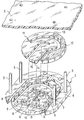
- FIG. 1 is an exploded perspective view of a first embodiment of the invention.
- FIG. 2 is a view analogous to FIG. 1, showing a second embodiment of the invention.
- the senor of the invention comprises, in conventional manner, a housing 1 with only a portion of its wall being shown in the figure, a cell given overall reference 2 being fixed to said portion by columns 3 .
- the cell 2 comprises a U-shaped support member 4 having a decoupling frame 5 carrying masses 6 and 7 interconnected by hinges 8 directly cut out in the plate forming the cell 2 .
- the cell has a vibrating member 9 in the form of a bar cut out in the plate and having its ends connected respectively to the masses 6 and 7 .
- the sensor also comprises a piezoelectric excitation circuit 16 shown in dashed lines in the figure, and a measurement circuit carried by the face of the cell opposite from the face that is visible in the figure.
- the senor further comprises a masking element 10 fixed to the end of a spiral-shaped link part 11 whose end opposite from the masking element 10 has a portion 12 of greater thickness defined by a shoulder 13 .
- the portion 12 of greater thickness shown cross-hatched in FIG. 1, is fixed to the inside face of the wall of the housing 1 , e.g. by adhesive, so that the remainder of the link part and the masking element 10 are spaced apart from the wall of the housing 1 by a distance that is equal to the height of the shoulder 13 .
- the masking element 10 is substantially rectangular in shape and covers not only the vibrating element 9 , but also an adjacent portion of the cell as indicated by chain-dotted lines in FIG. 1.
- the link part which surrounds the masking element 10 also extends over a portion of the cell adjacent to the vibrating member 9 .
- the wall of the housing behaves as a source of heat, and heat is thus transferred between the wall of the housing 1 and the cell 2 not only by conduction via the columns 3 , but also by radiation.
- the masking element 10 which is interposed between the wall of the housing 1 and the cell 2 , thus protects the vibrating member 9 against radiation so long as the temperature of the masking element 10 is no greater than that of the vibrating member 9 .
- the masking element 10 heats up progressively, not only under the effect of heat being transferred by radiation between the wall of the housing 1 and the masking element 10 , but also under the effect of heat being transferred by conduction due to the portion 12 of greater thickness being in contact with the wall of the housing 1 .
- This transfer of heat by conduction takes place via the link part 11 .
- the link part 11 is made of an appropriate material, and presents a cross-section and a length that are adapted to control heating of the masking element 10 by conduction so that the temperature rise of the masking element 10 is itself matched to the temperature rise of the remainder of the cell so that the temperature rise of the cell as a whole is more or less uniform under the effect of the various transfers of heat to which the cell is subjected.
- the thickness of the masking element is also determined as a function of the respective shapes of the masking element 10 , of the link part 11 , and of the cell 2 .
- a shield as shown in FIG. 1 has been made out of glass with a thickness of 100 ⁇ m.
- the effectiveness of the shield can be improved by a reflective coating 14 on the face of the masking element 10 which faces the vibrating member 9 .
- This reflective coating can be made by vacuum depositing a thin layer of gold on the masking element 10 , and where necessary on part or all of the link part 11 .
- FIG. 2 shows a second embodiment of the invention in which the masking element 10 fixed to the housing is replaced by a masking element formed by a reflective layer 15 covering the vibrating member 9 .
- the reflective layer 15 may also cover an adjacent part of the cell, for example the masses 6 and 7 and also the hinges 8 .
- This embodiment of the masking element presents the advantage of being isolated from any transfer of heat by conduction.
- the shield in the first embodiment is shown as being fixed to the housing 1 , the shield could equally well be fixed to the cell. In which case, it is nevertheless appropriate to ensure that the shield is spaced apart from the vibrating member sufficiently to avoid interfering with the mechanical operation of the vibrating member.
- the masking element may also be carried by the cell, by being made integrally with the cell during manufacture thereof.
- masking elements can be provided on both sides of the cell so as to protect the vibrating element 9 against radiation coming from the facing walls of the housing 1 .
- the electrodes which extend over one of the faces of the cell are generally made in the form of a reflective layer of gold, so the face of the cell carrying the electrodes has a smaller requirement for protection against heat transfer by radiation than does the opposite face.
- dimensions should be determined as a function of the thermal budget that results from the structure of the cell and the configuration of the housing relative to the cell.
- the spacing between the wall of the housing and the masking element 10 in the embodiment of FIG. 1 is shown as being obtained by a portion of greater thickness of the link part, this spacing may be obtained by means of a spacer, or merely by the thickness of the layer of adhesive that is used for fixing the link part to the wall of the housing.
- the invention is described in the context of a suspended-mass accelerometer, the invention is applicable to any vibrating sensor in which the vibrating element runs the risk of being subjected to differential stresses relative to the support member because of nonuniform transfers of heat over the various portions of the sensor.
- the invention is applicable to a star gyro, in particular a gyro as defined in patent document FR-A-2 741 151.
- the invention applies regardless of the structure of the cell, including when the cell does not have an intermediate frame.
Abstract
Description
- The present invention relates to a vibrating sensor, in particular an accelerometer or a gyro.
- The invention relates more particularly to sensors comprising a sensing cell in the form of a plate having defined therein a portion forming a support member and at least one vibrating element associated with excitation means. The excitation means enable the vibrating element to be set into vibration and enable the frequency of vibration thereof to be detected.
- In an accelerometer, the inertial element is connected to the vibrating element. In most cases, the inertial element is a mass, which is itself defined in the plate and movable relative to the support member. When the sensor is subjected to an acceleration, the mass exerts a force on the vibrating element. This force modifies the frequency of vibration in such a manner that the variation in the frequency of vibration of the vibrating element enables the acceleration to which the sensor is subjected to be determined.
- In order to avoid mechanical coupling between the vibrating element and the support member, it is general practice to provide an intermediate frame. Such mechanical isolation also lengthens the heat transfer path. This presents the advantage of ensuring that the temperature of the vibrating element is more uniform, thereby decreasing stresses of thermal origin and the associated parasitic effects. In spite of such arrangements, it has been found that variation in the frequency of vibration of the vibrating element continues to occur independently of variation in the acceleration to which the sensor is subjected, thus giving rise to parasitic variations in frequency interfering with the measurement of acceleration. So long as such parasitic variations exist they reduce the accuracy with which acceleration is measured.
- The present invention is based on the observation that has never been made before, whereby the temperature difference between various portions of the cell, and in particular between the vibrating member and the support member or the measurement mass results, in non-negligible manner, from an exchange of heat by radiation between the cell and the housing surrounding the cell. In particular, when the housing is at a higher temperature than the cell, the housing behaves as a source of heat which progressively raises the temperature of the cell by radiation. Those portions of the cell that have the smallest thermal inertia, and in particular the vibrating member, are thus raised to the temperature of the housing more quickly than other portions, thereby giving rise to stresses between the various portions of the cell, and thus to a variation in the frequency of vibration of the vibrating element.
- On the basis of these original observations, which form part of the invention, an object of the invention is to reduce parasitic variations in frequency that result from heat exchange by radiation inside the sensor.
- The invention provides a vibrating sensor comprising a cell fixed in a housing, the cell having a support member and a vibrating member connected to the support member and powered by an excitation circuit so as to be sensitive to the movements to which the sensor is subjected, the sensor including at least one thermal masking element independent of the excitation circuit and extending between the vibrating member and at least one wall of the housing.
- Thus, the thermal masking element stops at least a fraction of the heat being transmitted by radiation between the housing and the vibrating member, so that the vibrating member is protected from being heated by radiation for long enough to enable those portions of the cell that have greater thermal inertia to rise in temperature in a manner that matches substantially the rise in temperature of the vibrating member.
- In a preferred embodiment of the sensor of the invention, the masking element is fixed to the housing while being spaced apart therefrom. Preferably, the masking element is connected to the housing by a link part presenting a cross-section and a length that are adapted to control heating of the masking element by conduction. This avoids the temperature of the masking element rising too quickly, since otherwise it would itself become a source of radiation relative to the cell.
- Other characteristics and advantages of the invention will appear on reading the following description of two particular, non-limiting embodiments of the invention given with reference to the accompanying figures, in which:
- FIG. 1 is an exploded perspective view of a first embodiment of the invention; and
- FIG. 2 is a view analogous to FIG. 1, showing a second embodiment of the invention.
- In the figures, the respective thicknesses of the various layers are not shown to scale so as to make the invention easier to understand.
- With reference to FIG. 1, the sensor of the invention comprises, in conventional manner, a
housing 1 with only a portion of its wall being shown in the figure, a cell givenoverall reference 2 being fixed to said portion bycolumns 3. - In the embodiment shown, the
cell 2 comprises aU-shaped support member 4 having a decouplingframe 5 carryingmasses hinges 8 directly cut out in the plate forming thecell 2. Also in conventional manner, the cell has a vibratingmember 9 in the form of a bar cut out in the plate and having its ends connected respectively to themasses piezoelectric excitation circuit 16 shown in dashed lines in the figure, and a measurement circuit carried by the face of the cell opposite from the face that is visible in the figure. - According to the invention, the sensor further comprises a
masking element 10 fixed to the end of a spiral-shaped link part 11 whose end opposite from themasking element 10 has aportion 12 of greater thickness defined by ashoulder 13. During assembly of the sensor, theportion 12 of greater thickness, shown cross-hatched in FIG. 1, is fixed to the inside face of the wall of thehousing 1, e.g. by adhesive, so that the remainder of the link part and themasking element 10 are spaced apart from the wall of thehousing 1 by a distance that is equal to the height of theshoulder 13. - In the embodiment shown, the
masking element 10 is substantially rectangular in shape and covers not only thevibrating element 9, but also an adjacent portion of the cell as indicated by chain-dotted lines in FIG. 1. In addition, the link part which surrounds themasking element 10 also extends over a portion of the cell adjacent to the vibratingmember 9. - When the temperature of the
housing 1 is higher than that of thecell 2, the wall of the housing behaves as a source of heat, and heat is thus transferred between the wall of thehousing 1 and thecell 2 not only by conduction via thecolumns 3, but also by radiation. Themasking element 10 which is interposed between the wall of thehousing 1 and thecell 2, thus protects the vibratingmember 9 against radiation so long as the temperature of themasking element 10 is no greater than that of the vibratingmember 9. In this context, it should be observed that themasking element 10 heats up progressively, not only under the effect of heat being transferred by radiation between the wall of thehousing 1 and themasking element 10, but also under the effect of heat being transferred by conduction due to theportion 12 of greater thickness being in contact with the wall of thehousing 1. This transfer of heat by conduction takes place via thelink part 11. - According to an aspect of the invention, the
link part 11 is made of an appropriate material, and presents a cross-section and a length that are adapted to control heating of themasking element 10 by conduction so that the temperature rise of themasking element 10 is itself matched to the temperature rise of the remainder of the cell so that the temperature rise of the cell as a whole is more or less uniform under the effect of the various transfers of heat to which the cell is subjected. - The thickness of the masking element is also determined as a function of the respective shapes of the
masking element 10, of thelink part 11, and of thecell 2. By way of non-limiting example, for a cell having the configuration shown in FIG. 1, and made out of a quartz crystal plate having a thickness of 500 micrometers (μm), a shield as shown in FIG. 1 has been made out of glass with a thickness of 100 μm. - It should be observed that in the opposite case where the housing is at a temperature lower than that of the
cell 2, exchange of heat by radiation reverses directions, with the wall of the housing then acting as a heat sink. In this case, the masking element acts as above to minimize transfers of heat by radiation. - The effectiveness of the shield can be improved by a
reflective coating 14 on the face of themasking element 10 which faces the vibratingmember 9. This reflective coating can be made by vacuum depositing a thin layer of gold on themasking element 10, and where necessary on part or all of thelink part 11. - FIG. 2 shows a second embodiment of the invention in which the
masking element 10 fixed to the housing is replaced by a masking element formed by areflective layer 15 covering the vibratingmember 9. As above, thereflective layer 15 may also cover an adjacent part of the cell, for example themasses hinges 8. This embodiment of the masking element presents the advantage of being isolated from any transfer of heat by conduction. - Naturally, the invention is not limited to the embodiments described and variants that can be applied thereto will appear to the person skilled in the art without going beyond the ambit of the invention as defined by the claims.
- In particular, although the shield in the first embodiment is shown as being fixed to the
housing 1, the shield could equally well be fixed to the cell. In which case, it is nevertheless appropriate to ensure that the shield is spaced apart from the vibrating member sufficiently to avoid interfering with the mechanical operation of the vibrating member. The masking element may also be carried by the cell, by being made integrally with the cell during manufacture thereof. - Although the invention is described in the context of embodiments in which there is a masking element on one side only of the cell, masking elements can be provided on both sides of the cell so as to protect the vibrating
element 9 against radiation coming from the facing walls of thehousing 1. Nevertheless, it should be observed that the electrodes which extend over one of the faces of the cell are generally made in the form of a reflective layer of gold, so the face of the cell carrying the electrodes has a smaller requirement for protection against heat transfer by radiation than does the opposite face. - When manufacturing the masking element(s), and where appropriate the link parts carrying them, dimensions should be determined as a function of the thermal budget that results from the structure of the cell and the configuration of the housing relative to the cell. Although the spacing between the wall of the housing and the
masking element 10 in the embodiment of FIG. 1 is shown as being obtained by a portion of greater thickness of the link part, this spacing may be obtained by means of a spacer, or merely by the thickness of the layer of adhesive that is used for fixing the link part to the wall of the housing. - Although the invention is described in the context of a suspended-mass accelerometer, the invention is applicable to any vibrating sensor in which the vibrating element runs the risk of being subjected to differential stresses relative to the support member because of nonuniform transfers of heat over the various portions of the sensor. In particular, the invention is applicable to a star gyro, in particular a gyro as defined in patent document FR-A-2 741 151.
- The invention applies regardless of the structure of the cell, including when the cell does not have an intermediate frame.
Claims (10)
Applications Claiming Priority (2)
| Application Number | Priority Date | Filing Date | Title |
|---|---|---|---|
| FR0302220A FR2851659B1 (en) | 2003-02-24 | 2003-02-24 | VIBRATORY SENSOR WITH RADIATION SCREEN |
| FR0302220 | 2003-02-24 |
Publications (2)
| Publication Number | Publication Date |
|---|---|
| US20040163473A1 true US20040163473A1 (en) | 2004-08-26 |
| US6948368B2 US6948368B2 (en) | 2005-09-27 |
Family
ID=32732056
Family Applications (1)
| Application Number | Title | Priority Date | Filing Date |
|---|---|---|---|
| US10/777,143 Expired - Fee Related US6948368B2 (en) | 2003-02-24 | 2004-02-13 | Vibrating sensor with thermal shield |
Country Status (3)
| Country | Link |
|---|---|
| US (1) | US6948368B2 (en) |
| EP (1) | EP1450164B1 (en) |
| FR (1) | FR2851659B1 (en) |
Cited By (1)
| Publication number | Priority date | Publication date | Assignee | Title |
|---|---|---|---|---|
| CN107607323A (en) * | 2017-10-11 | 2018-01-19 | 内蒙航天动力机械测试所 | A kind of fireproof covering of vibrating sensor |
Families Citing this family (2)
| Publication number | Priority date | Publication date | Assignee | Title |
|---|---|---|---|---|
| FR2887990B1 (en) | 2005-07-04 | 2007-09-07 | Sagem Defense Securite | INERTIAL SENSOR WITH REDUCING CURRENT CURRENT BY REDUCING WIDTH AND TRACK CLEARANCE IN CRITICAL AREAS |
| FR2887989B1 (en) * | 2005-07-04 | 2007-09-07 | Sagem Defense Securite | INERTIAL SENSOR WITH REDUCER CURRENT REDUCED BY COMPENSATION BRANCHES |
Citations (12)
| Publication number | Priority date | Publication date | Assignee | Title |
|---|---|---|---|---|
| US3702073A (en) * | 1969-02-28 | 1972-11-07 | Sundstrand Data Control | Accelerometer |
| US4592234A (en) * | 1984-06-11 | 1986-06-03 | Sundstrand Data Control, Inc. | Suspension system for a transducer |
| US4912990A (en) * | 1989-02-27 | 1990-04-03 | Sundstrand Data Control, Inc. | Magnetically driven vibrating beam force transducer |
| US5058430A (en) * | 1989-12-29 | 1991-10-22 | Honeywell Inc. | Sensor capsule mounting |
| US5188983A (en) * | 1990-04-11 | 1993-02-23 | Wisconsin Alumni Research Foundation | Polysilicon resonating beam transducers and method of producing the same |
| US5417115A (en) * | 1993-07-23 | 1995-05-23 | Honeywell Inc. | Dielectrically isolated resonant microsensors |
| US5458000A (en) * | 1993-07-20 | 1995-10-17 | Honeywell Inc. | Static pressure compensation of resonant integrated microbeam sensors |
| US5559358A (en) * | 1993-05-25 | 1996-09-24 | Honeywell Inc. | Opto-electro-mechanical device or filter, process for making, and sensors made therefrom |
| US5600067A (en) * | 1993-08-18 | 1997-02-04 | Alliedsignal, Inc. | Torque wire thermal strain relief |
| US5644083A (en) * | 1994-06-29 | 1997-07-01 | New Sd, Inc. | Accelerometer and method of manufacture |
| US5962786A (en) * | 1995-09-26 | 1999-10-05 | Onera (Office National D'eudes Et De Recheres Aerospatiales) | Monolithic accelerometric transducer |
| US6161440A (en) * | 1997-08-14 | 2000-12-19 | Alliedsignal Inc. | Low metalization creep sensor |
Family Cites Families (1)
| Publication number | Priority date | Publication date | Assignee | Title |
|---|---|---|---|---|
| JPH09105636A (en) * | 1995-10-12 | 1997-04-22 | Murata Mfg Co Ltd | Vibrating gyro |
-
2003
- 2003-02-24 FR FR0302220A patent/FR2851659B1/en not_active Expired - Fee Related
-
2004
- 2004-02-10 EP EP04290339.3A patent/EP1450164B1/en not_active Expired - Lifetime
- 2004-02-13 US US10/777,143 patent/US6948368B2/en not_active Expired - Fee Related
Patent Citations (12)
| Publication number | Priority date | Publication date | Assignee | Title |
|---|---|---|---|---|
| US3702073A (en) * | 1969-02-28 | 1972-11-07 | Sundstrand Data Control | Accelerometer |
| US4592234A (en) * | 1984-06-11 | 1986-06-03 | Sundstrand Data Control, Inc. | Suspension system for a transducer |
| US4912990A (en) * | 1989-02-27 | 1990-04-03 | Sundstrand Data Control, Inc. | Magnetically driven vibrating beam force transducer |
| US5058430A (en) * | 1989-12-29 | 1991-10-22 | Honeywell Inc. | Sensor capsule mounting |
| US5188983A (en) * | 1990-04-11 | 1993-02-23 | Wisconsin Alumni Research Foundation | Polysilicon resonating beam transducers and method of producing the same |
| US5559358A (en) * | 1993-05-25 | 1996-09-24 | Honeywell Inc. | Opto-electro-mechanical device or filter, process for making, and sensors made therefrom |
| US5458000A (en) * | 1993-07-20 | 1995-10-17 | Honeywell Inc. | Static pressure compensation of resonant integrated microbeam sensors |
| US5417115A (en) * | 1993-07-23 | 1995-05-23 | Honeywell Inc. | Dielectrically isolated resonant microsensors |
| US5600067A (en) * | 1993-08-18 | 1997-02-04 | Alliedsignal, Inc. | Torque wire thermal strain relief |
| US5644083A (en) * | 1994-06-29 | 1997-07-01 | New Sd, Inc. | Accelerometer and method of manufacture |
| US5962786A (en) * | 1995-09-26 | 1999-10-05 | Onera (Office National D'eudes Et De Recheres Aerospatiales) | Monolithic accelerometric transducer |
| US6161440A (en) * | 1997-08-14 | 2000-12-19 | Alliedsignal Inc. | Low metalization creep sensor |
Cited By (1)
| Publication number | Priority date | Publication date | Assignee | Title |
|---|---|---|---|---|
| CN107607323A (en) * | 2017-10-11 | 2018-01-19 | 内蒙航天动力机械测试所 | A kind of fireproof covering of vibrating sensor |
Also Published As
| Publication number | Publication date |
|---|---|
| FR2851659B1 (en) | 2005-06-24 |
| EP1450164A1 (en) | 2004-08-25 |
| FR2851659A1 (en) | 2004-08-27 |
| US6948368B2 (en) | 2005-09-27 |
| EP1450164B1 (en) | 2013-07-24 |
Similar Documents
| Publication | Publication Date | Title |
|---|---|---|
| US20040041248A1 (en) | Packaged microchip with isolation | |
| CN105705926B (en) | Pressure sensor including the structure for being used to control the adhesive phase of tolerable temperature variation | |
| ITUA20163990A1 (en) | MINIATURIZED LOAD SENSOR DEVICE WITH REDUCED SENSITIVITY TO THERMO-MECHANICAL STRENGTHENING OF STRENGTHENING, IN PARTICULAR STRENGTH AND PRESSURE SENSOR | |
| US7798010B2 (en) | Sensor geometry for improved package stress isolation | |
| US6662655B2 (en) | Net zero isolator | |
| US6948368B2 (en) | Vibrating sensor with thermal shield | |
| JPH09105690A (en) | Pressure sensor having decreased hysteresis and improved electric performance at low pressure | |
| JPH06291334A (en) | Acceleration sensor | |
| JP2006153519A (en) | Acceleration sensor | |
| JPS6318271A (en) | Piezoelectric type mechanical quantity sensor | |
| JP3368744B2 (en) | Vibration acceleration sensor | |
| JPH02248866A (en) | Beam construction for acceleration sensor | |
| CN111239439B (en) | Vibration type sensor device | |
| US20220219971A1 (en) | Multiply encapsulated micro electrical mechanical systems device | |
| JP5194510B2 (en) | Sensor device | |
| US7022990B2 (en) | Deep cavity sensor package | |
| JP2010210402A (en) | Mems sensor | |
| JP2013217719A (en) | Pressure sensor and electronic apparatus | |
| JP2003075467A (en) | Electrostatic capacitive accelerometer | |
| JPH0682131B2 (en) | Vibration acceleration sensor | |
| JP2003207516A (en) | Semiconductor acceleration sensor and method of manufacturing the same | |
| JPH11311631A (en) | Semiconductor accelerometer | |
| JP2006153516A (en) | Acceleration sensor | |
| JPH06137935A (en) | Infrared sensor | |
| JPH11311630A (en) | Semiconductor accelerometer |
Legal Events
| Date | Code | Title | Description |
|---|---|---|---|
| AS | Assignment |
Owner name: SAGEM SA, FRANCE Free format text: ASSIGNMENT OF ASSIGNORS INTEREST;ASSIGNOR:ONFROY, PHILIPPE;REEL/FRAME:014987/0478 Effective date: 20031205 |
|
| AS | Assignment |
Owner name: SAGEM DEFENSE SECURITE, FRANCE Free format text: ASSIGNMENT OF ASSIGNORS INTEREST;ASSIGNOR:SAGEM SA;REEL/FRAME:016609/0004 Effective date: 20050728 |
|
| FEPP | Fee payment procedure |
Free format text: PAYOR NUMBER ASSIGNED (ORIGINAL EVENT CODE: ASPN); ENTITY STATUS OF PATENT OWNER: LARGE ENTITY |
|
| FEPP | Fee payment procedure |
Free format text: PAYOR NUMBER ASSIGNED (ORIGINAL EVENT CODE: ASPN); ENTITY STATUS OF PATENT OWNER: LARGE ENTITY Free format text: PAYER NUMBER DE-ASSIGNED (ORIGINAL EVENT CODE: RMPN); ENTITY STATUS OF PATENT OWNER: LARGE ENTITY |
|
| FPAY | Fee payment |
Year of fee payment: 4 |
|
| REMI | Maintenance fee reminder mailed | ||
| LAPS | Lapse for failure to pay maintenance fees | ||
| STCH | Information on status: patent discontinuation |
Free format text: PATENT EXPIRED DUE TO NONPAYMENT OF MAINTENANCE FEES UNDER 37 CFR 1.362 |
|
| FP | Lapsed due to failure to pay maintenance fee |
Effective date: 20130927 |