US20040095297A1 - Nonlinear voltage controlled current source with feedback circuit - Google Patents
Nonlinear voltage controlled current source with feedback circuit Download PDFInfo
- Publication number
- US20040095297A1 US20040095297A1 US10/300,640 US30064002A US2004095297A1 US 20040095297 A1 US20040095297 A1 US 20040095297A1 US 30064002 A US30064002 A US 30064002A US 2004095297 A1 US2004095297 A1 US 2004095297A1
- Authority
- US
- United States
- Prior art keywords
- current
- usec
- current source
- light emitting
- pixel
- Prior art date
- Legal status (The legal status is an assumption and is not a legal conclusion. Google has not performed a legal analysis and makes no representation as to the accuracy of the status listed.)
- Abandoned
Links
Images


Classifications
-
- G—PHYSICS
- G09—EDUCATION; CRYPTOGRAPHY; DISPLAY; ADVERTISING; SEALS
- G09G—ARRANGEMENTS OR CIRCUITS FOR CONTROL OF INDICATING DEVICES USING STATIC MEANS TO PRESENT VARIABLE INFORMATION
- G09G3/00—Control arrangements or circuits, of interest only in connection with visual indicators other than cathode-ray tubes
- G09G3/20—Control arrangements or circuits, of interest only in connection with visual indicators other than cathode-ray tubes for presentation of an assembly of a number of characters, e.g. a page, by composing the assembly by combination of individual elements arranged in a matrix no fixed position being assigned to or needed to be assigned to the individual characters or partial characters
- G09G3/22—Control arrangements or circuits, of interest only in connection with visual indicators other than cathode-ray tubes for presentation of an assembly of a number of characters, e.g. a page, by composing the assembly by combination of individual elements arranged in a matrix no fixed position being assigned to or needed to be assigned to the individual characters or partial characters using controlled light sources
- G09G3/30—Control arrangements or circuits, of interest only in connection with visual indicators other than cathode-ray tubes for presentation of an assembly of a number of characters, e.g. a page, by composing the assembly by combination of individual elements arranged in a matrix no fixed position being assigned to or needed to be assigned to the individual characters or partial characters using controlled light sources using electroluminescent panels
- G09G3/32—Control arrangements or circuits, of interest only in connection with visual indicators other than cathode-ray tubes for presentation of an assembly of a number of characters, e.g. a page, by composing the assembly by combination of individual elements arranged in a matrix no fixed position being assigned to or needed to be assigned to the individual characters or partial characters using controlled light sources using electroluminescent panels semiconductive, e.g. using light-emitting diodes [LED]
- G09G3/3208—Control arrangements or circuits, of interest only in connection with visual indicators other than cathode-ray tubes for presentation of an assembly of a number of characters, e.g. a page, by composing the assembly by combination of individual elements arranged in a matrix no fixed position being assigned to or needed to be assigned to the individual characters or partial characters using controlled light sources using electroluminescent panels semiconductive, e.g. using light-emitting diodes [LED] organic, e.g. using organic light-emitting diodes [OLED]
- G09G3/3225—Control arrangements or circuits, of interest only in connection with visual indicators other than cathode-ray tubes for presentation of an assembly of a number of characters, e.g. a page, by composing the assembly by combination of individual elements arranged in a matrix no fixed position being assigned to or needed to be assigned to the individual characters or partial characters using controlled light sources using electroluminescent panels semiconductive, e.g. using light-emitting diodes [LED] organic, e.g. using organic light-emitting diodes [OLED] using an active matrix
- G09G3/3233—Control arrangements or circuits, of interest only in connection with visual indicators other than cathode-ray tubes for presentation of an assembly of a number of characters, e.g. a page, by composing the assembly by combination of individual elements arranged in a matrix no fixed position being assigned to or needed to be assigned to the individual characters or partial characters using controlled light sources using electroluminescent panels semiconductive, e.g. using light-emitting diodes [LED] organic, e.g. using organic light-emitting diodes [OLED] using an active matrix with pixel circuitry controlling the current through the light-emitting element
- G09G3/3241—Control arrangements or circuits, of interest only in connection with visual indicators other than cathode-ray tubes for presentation of an assembly of a number of characters, e.g. a page, by composing the assembly by combination of individual elements arranged in a matrix no fixed position being assigned to or needed to be assigned to the individual characters or partial characters using controlled light sources using electroluminescent panels semiconductive, e.g. using light-emitting diodes [LED] organic, e.g. using organic light-emitting diodes [OLED] using an active matrix with pixel circuitry controlling the current through the light-emitting element the current through the light-emitting element being set using a data current provided by the data driver, e.g. by using a two-transistor current mirror
- G09G3/325—Control arrangements or circuits, of interest only in connection with visual indicators other than cathode-ray tubes for presentation of an assembly of a number of characters, e.g. a page, by composing the assembly by combination of individual elements arranged in a matrix no fixed position being assigned to or needed to be assigned to the individual characters or partial characters using controlled light sources using electroluminescent panels semiconductive, e.g. using light-emitting diodes [LED] organic, e.g. using organic light-emitting diodes [OLED] using an active matrix with pixel circuitry controlling the current through the light-emitting element the current through the light-emitting element being set using a data current provided by the data driver, e.g. by using a two-transistor current mirror the data current flowing through the driving transistor during a setting phase, e.g. by using a switch for connecting the driving transistor to the data driver
-
- G—PHYSICS
- G09—EDUCATION; CRYPTOGRAPHY; DISPLAY; ADVERTISING; SEALS
- G09G—ARRANGEMENTS OR CIRCUITS FOR CONTROL OF INDICATING DEVICES USING STATIC MEANS TO PRESENT VARIABLE INFORMATION
- G09G3/00—Control arrangements or circuits, of interest only in connection with visual indicators other than cathode-ray tubes
- G09G3/20—Control arrangements or circuits, of interest only in connection with visual indicators other than cathode-ray tubes for presentation of an assembly of a number of characters, e.g. a page, by composing the assembly by combination of individual elements arranged in a matrix no fixed position being assigned to or needed to be assigned to the individual characters or partial characters
- G09G3/22—Control arrangements or circuits, of interest only in connection with visual indicators other than cathode-ray tubes for presentation of an assembly of a number of characters, e.g. a page, by composing the assembly by combination of individual elements arranged in a matrix no fixed position being assigned to or needed to be assigned to the individual characters or partial characters using controlled light sources
- G09G3/30—Control arrangements or circuits, of interest only in connection with visual indicators other than cathode-ray tubes for presentation of an assembly of a number of characters, e.g. a page, by composing the assembly by combination of individual elements arranged in a matrix no fixed position being assigned to or needed to be assigned to the individual characters or partial characters using controlled light sources using electroluminescent panels
- G09G3/32—Control arrangements or circuits, of interest only in connection with visual indicators other than cathode-ray tubes for presentation of an assembly of a number of characters, e.g. a page, by composing the assembly by combination of individual elements arranged in a matrix no fixed position being assigned to or needed to be assigned to the individual characters or partial characters using controlled light sources using electroluminescent panels semiconductive, e.g. using light-emitting diodes [LED]
- G09G3/3208—Control arrangements or circuits, of interest only in connection with visual indicators other than cathode-ray tubes for presentation of an assembly of a number of characters, e.g. a page, by composing the assembly by combination of individual elements arranged in a matrix no fixed position being assigned to or needed to be assigned to the individual characters or partial characters using controlled light sources using electroluminescent panels semiconductive, e.g. using light-emitting diodes [LED] organic, e.g. using organic light-emitting diodes [OLED]
- G09G3/3275—Details of drivers for data electrodes
- G09G3/3283—Details of drivers for data electrodes in which the data driver supplies a variable data current for setting the current through, or the voltage across, the light-emitting elements
-
- G—PHYSICS
- G09—EDUCATION; CRYPTOGRAPHY; DISPLAY; ADVERTISING; SEALS
- G09G—ARRANGEMENTS OR CIRCUITS FOR CONTROL OF INDICATING DEVICES USING STATIC MEANS TO PRESENT VARIABLE INFORMATION
- G09G2300/00—Aspects of the constitution of display devices
- G09G2300/04—Structural and physical details of display devices
- G09G2300/0404—Matrix technologies
- G09G2300/0408—Integration of the drivers onto the display substrate
-
- G—PHYSICS
- G09—EDUCATION; CRYPTOGRAPHY; DISPLAY; ADVERTISING; SEALS
- G09G—ARRANGEMENTS OR CIRCUITS FOR CONTROL OF INDICATING DEVICES USING STATIC MEANS TO PRESENT VARIABLE INFORMATION
- G09G2300/00—Aspects of the constitution of display devices
- G09G2300/08—Active matrix structure, i.e. with use of active elements, inclusive of non-linear two terminal elements, in the pixels together with light emitting or modulating elements
- G09G2300/0809—Several active elements per pixel in active matrix panels
- G09G2300/0819—Several active elements per pixel in active matrix panels used for counteracting undesired variations, e.g. feedback or autozeroing
-
- G—PHYSICS
- G09—EDUCATION; CRYPTOGRAPHY; DISPLAY; ADVERTISING; SEALS
- G09G—ARRANGEMENTS OR CIRCUITS FOR CONTROL OF INDICATING DEVICES USING STATIC MEANS TO PRESENT VARIABLE INFORMATION
- G09G2300/00—Aspects of the constitution of display devices
- G09G2300/08—Active matrix structure, i.e. with use of active elements, inclusive of non-linear two terminal elements, in the pixels together with light emitting or modulating elements
- G09G2300/0809—Several active elements per pixel in active matrix panels
- G09G2300/0842—Several active elements per pixel in active matrix panels forming a memory circuit, e.g. a dynamic memory with one capacitor
-
- G—PHYSICS
- G09—EDUCATION; CRYPTOGRAPHY; DISPLAY; ADVERTISING; SEALS
- G09G—ARRANGEMENTS OR CIRCUITS FOR CONTROL OF INDICATING DEVICES USING STATIC MEANS TO PRESENT VARIABLE INFORMATION
- G09G2310/00—Command of the display device
- G09G2310/02—Addressing, scanning or driving the display screen or processing steps related thereto
- G09G2310/0243—Details of the generation of driving signals
- G09G2310/0248—Precharge or discharge of column electrodes before or after applying exact column voltages
-
- G—PHYSICS
- G09—EDUCATION; CRYPTOGRAPHY; DISPLAY; ADVERTISING; SEALS
- G09G—ARRANGEMENTS OR CIRCUITS FOR CONTROL OF INDICATING DEVICES USING STATIC MEANS TO PRESENT VARIABLE INFORMATION
- G09G2320/00—Control of display operating conditions
- G09G2320/02—Improving the quality of display appearance
- G09G2320/0219—Reducing feedthrough effects in active matrix panels, i.e. voltage changes on the scan electrode influencing the pixel voltage due to capacitive coupling
-
- G—PHYSICS
- G09—EDUCATION; CRYPTOGRAPHY; DISPLAY; ADVERTISING; SEALS
- G09G—ARRANGEMENTS OR CIRCUITS FOR CONTROL OF INDICATING DEVICES USING STATIC MEANS TO PRESENT VARIABLE INFORMATION
- G09G2320/00—Control of display operating conditions
- G09G2320/02—Improving the quality of display appearance
- G09G2320/0233—Improving the luminance or brightness uniformity across the screen
-
- G—PHYSICS
- G09—EDUCATION; CRYPTOGRAPHY; DISPLAY; ADVERTISING; SEALS
- G09G—ARRANGEMENTS OR CIRCUITS FOR CONTROL OF INDICATING DEVICES USING STATIC MEANS TO PRESENT VARIABLE INFORMATION
- G09G2320/00—Control of display operating conditions
- G09G2320/02—Improving the quality of display appearance
- G09G2320/0252—Improving the response speed
-
- G—PHYSICS
- G09—EDUCATION; CRYPTOGRAPHY; DISPLAY; ADVERTISING; SEALS
- G09G—ARRANGEMENTS OR CIRCUITS FOR CONTROL OF INDICATING DEVICES USING STATIC MEANS TO PRESENT VARIABLE INFORMATION
- G09G2320/00—Control of display operating conditions
- G09G2320/02—Improving the quality of display appearance
- G09G2320/029—Improving the quality of display appearance by monitoring one or more pixels in the display panel, e.g. by monitoring a fixed reference pixel
-
- G—PHYSICS
- G09—EDUCATION; CRYPTOGRAPHY; DISPLAY; ADVERTISING; SEALS
- G09G—ARRANGEMENTS OR CIRCUITS FOR CONTROL OF INDICATING DEVICES USING STATIC MEANS TO PRESENT VARIABLE INFORMATION
- G09G2320/00—Control of display operating conditions
- G09G2320/04—Maintaining the quality of display appearance
- G09G2320/043—Preventing or counteracting the effects of ageing
-
- G—PHYSICS
- G09—EDUCATION; CRYPTOGRAPHY; DISPLAY; ADVERTISING; SEALS
- G09G—ARRANGEMENTS OR CIRCUITS FOR CONTROL OF INDICATING DEVICES USING STATIC MEANS TO PRESENT VARIABLE INFORMATION
- G09G2320/00—Control of display operating conditions
- G09G2320/06—Adjustment of display parameters
- G09G2320/0626—Adjustment of display parameters for control of overall brightness
-
- G—PHYSICS
- G09—EDUCATION; CRYPTOGRAPHY; DISPLAY; ADVERTISING; SEALS
- G09G—ARRANGEMENTS OR CIRCUITS FOR CONTROL OF INDICATING DEVICES USING STATIC MEANS TO PRESENT VARIABLE INFORMATION
- G09G2360/00—Aspects of the architecture of display systems
- G09G2360/14—Detecting light within display terminals, e.g. using a single or a plurality of photosensors
- G09G2360/145—Detecting light within display terminals, e.g. using a single or a plurality of photosensors the light originating from the display screen
- G09G2360/147—Detecting light within display terminals, e.g. using a single or a plurality of photosensors the light originating from the display screen the originated light output being determined for each pixel
-
- G—PHYSICS
- G09—EDUCATION; CRYPTOGRAPHY; DISPLAY; ADVERTISING; SEALS
- G09G—ARRANGEMENTS OR CIRCUITS FOR CONTROL OF INDICATING DEVICES USING STATIC MEANS TO PRESENT VARIABLE INFORMATION
- G09G3/00—Control arrangements or circuits, of interest only in connection with visual indicators other than cathode-ray tubes
- G09G3/20—Control arrangements or circuits, of interest only in connection with visual indicators other than cathode-ray tubes for presentation of an assembly of a number of characters, e.g. a page, by composing the assembly by combination of individual elements arranged in a matrix no fixed position being assigned to or needed to be assigned to the individual characters or partial characters
- G09G3/2007—Display of intermediate tones
- G09G3/2011—Display of intermediate tones by amplitude modulation
Definitions
- the present invention relates to light emitting diode displays and to particular types of diodes useful for such displays, known as organic light emitting diodes OLED and a variation thereof; i.e., known as AMOLED, the AM standing for active matrix.
- OLED organic light emitting diodes
- AMOLED the AM standing for active matrix
- AMOLED active matrix organic light emitting diode
- the OLED is a current mode device such that the gray scale illumination is proportional to current flowing through the OLED, with current accuracy and matching of 1% or less desired, and
- TFT thin film transistor
- a-Si morphous silicon
- poly-Si poly-silicon
- organic such as pentacene
- CdSe Cadmiun Selenium
- AMOLED displays Like other flat panel displays such as those having LCDs, AMOLED displays also exhibit some common undesirable issues, such as the fact that thin film transistor (TFT) technologies used today for active matrix displays all exhibit device degradation, with one of the main components being transistor threshold voltage shift with operation time.
- TFT thin film transistor
- a primary object of the present invention is to enable quick charging of the high parasitic capacitance associated with the above described diodes, and immediately provide the steady state current needed in the pixel circuit.
- a broad feature of the present invention resides in the provision, in a pixel circuit, of a voltage controlled current source using nonlinear feedback for rapidly charging parasitic capacitance.
- the current feedback arrangement by dint of a suitably provided current sense means, will not only automatically provide the nonlinear current flow (versus constant) for charging up the parasitic capacitance quickly, but will also immediately produce, after the capacitance charging takes place, a steady state (constant current) with minimum ringing to a predefined desired current level, thereby enabling proper light emission.
- this predefined current level is proportional to the threshold voltage of the thin film transistor (TFT) being monitored, and will thus adjust to the new threshold voltage value brought on by TFT aging.
- TFT thin film transistor
- Such architecture and technique is extremely useful for driving OLEDs, where the relatively large (approximately 6 pF/pixel) turn-on parasitic capacitance needs to be charged before on current flow for rumination takes place, and where increasing duty cycle (greater than 50% range) is expected to cause instabilities resulting in TFT threshold voltage shifts.
- This architecture is well suited for implementation into OLED data current driver chips or integrated driver circuitry.
- FIG. 1 is a block diagram of the scheme of meeting the described issues and/or problems present as certain light emitting diode displays
- FIG. 2 is a more detailed schematic diagram of an implementation of the system of FIG. 1;
- FIG. 3 is a graph defining VT′ in relationship to the linear extrapolated value of VT′ where VT′ is the value of V OUT shown in the circuit of FIG. 2;
- FIG. 4 is a graph of V OUT versus time (t).
- FIGS. 5A, 5B, 6 A and 6 B are various graphs of current charging times.
- FIG. 1 the block diagram of the disclosed architecture capable of meeting the issues discussed above is shown in FIG. 1, with an equivalent detailed circuit implementation shown in FIG. 2.
- an OLED pixel illumination mode would require a constant gate voltage on the driver TFT T1, such as, but not limited to ground, and the source voltage adjusts to a value so that Vgs supports a predetermined current value.
- the “threshold voltage” defined by this predetermined current value is negative of the source voltage.
- the current source 20 is intended to provide a high output impedance and bi-directional current.
- the feedback settling time and the charging of the parasitic capacitance account for a finite but small delay.
- the current source and/or the current feedback 40 can be implemented in the pixel or in the peripheral circuitry of the array, including but not limited to the display data current driver chips.
- FIG. 2 shows one possible circuit implementation from the architecture disclosed in FIG. 1, that can be implemented in the data current drivers.
- all switches SW1, SW3-1 and SW3-2—are set to the ground pole, including the pixel TFTs T1 and T3.
- all switches are set to the pole other than ground, including the pixel TFT T3, with the gates high (N-channel). Note that TFT T1 gate remains grounded since the feedback circuit dynamic range covers both positive and negative, and hence TFT T1 will be turned on by having the source pulled negative to a voltage that will support the constant current.
- the current source is formed by operational amplifiers 3 and 4 which operate as well to provide a unity gain buffer for the source of the OLED under illumination.
- Opamp 1 and 2 constitute a current sense amplifier 50 and are used as a proportional feedback element for the current source voltage reference Vref.
- the current source 20 senses the threshold at a predefined current level. The feedback increases the current source output current, for zero drain voltage, for example, by a factor of 10 or more; this is in order to facilitate the charging of parasitic and stray capacitances at the data line 30 and the pixel 10 , before the appropriate current reference I REF is established through T1 and T2.
- the feedback arrangement ensures that the current through T1 and T2 is monotonically increasing up to the appropriate current reference level.
- the current source current decrease so as to minimize any voltage overshoot across the gate-to-source of T1.
- the current source current decreases by a factor related to [1+R D /R S (1+R F /R 1 )].
- C S is the parasitic capacitance, including the data line and pixel parasitic capacitance, that the driver TFT, T2, must charge
- ⁇ is the TFT device transconductance parameter equal to ⁇ n C in W/L , which is the product of TFT channel mobility, gate insulator capacitance, width and length of the channel.
- the other resistances and voltages are defined in FIG. 2.
- ⁇ ⁇ 2 ⁇ C s ⁇ ⁇ R D R S ⁇ ( 1 + R F R 1 ) + 1 ⁇
- the method is capable of meeting several AMOLED specifications, namely:
- one approach uses a column driver chip and circuit therein for reserving a constant time portion of the scan cycle to precharge the columns to a voltage threshold that is just below the onset of conduction.
- the driver circuit applies a precision, but constant on current that is pulse width modulated to give an integrated current density proportional to the desired OLED light output.
- the disclosed approach differs substantially and has the advantages of (1) uses only one time portion (verus two), (2) using a nonlinear (versus constant) current amplitude, and (3) using current amplitude modulation (versus pulse width modulation).
- the advantages of (1), or of using only one time portion is that there is more time available for OLED luminance, and since the output luminance is proportional to the integrated current density over the frame cycle, a lower amplitude current is needed to achieve the same integrated current density.
- the OLED is more power efficient operating at lower current density.
- the advantage of (2), or using a nonlinear current amplitude is that precharge time is minimized and independent of colors.
- the data line capacitance to the pixel will vary dependent on the pixel location from the data current driver source, so minimizing the data line parasitic charging leaves more time for pixel capacitance charging, resulting in more accuracy.
- the advantage of (3), of using current amplitude modulation is that the entire scan time is available for OLED luminance, and as stated above, since the output luminance is proportional to the integrated current density over the frame cycle, a lower amplitude current is needed to achieve the same integrated current density, thus providing a more power efficient drive method.
- Table 1 shows the range of the nonlinear current source pixel feedback circuit for various parameters.
- Rows 7 through 10 correspond to the four rows 3 through 6 (blue) with the threshold voltage of M2 in the pixel now shifted by 5V, from a Vt of 2V to a V5 of 7V, which now ranges from a charging time of 1.0 usec to 1.6 usec. If an even faster charging time is desired, Vdd may be increased, for example from 5V to 10V. Rows 13 through 16 correspond to the earlier rows 7, 10, 3, 6, respectively, where the charging time is now decreased to the range from 0.4 usec to 0.9 usec. ⁇ Vgs and Vdd signifies the negative and positive-most voltages in the circuit.
- Vdd needs to be set externally since ⁇ Vgs is the negative of the Vgs of M2 needed to sustain the targeted pixel current, where the gate voltage is ground.
- FIG. 5 a and 5 b show the dependency of the line capacitance over a range of 10 pF to 50 pF on the charge up time verus the pixel current and pixel voltage reference error, respectively.
- the three set of curves correspond to rows 1 through 3 of Table 1.
- FIG. 6 a and 6 b show the dependency of the pixel current over a range of 10 nA to 10 uA on the charge up time verus the pixel current and pixel voltage reference error, respectively, for a situation after a 5V TFT threshold voltage shift.
- the four sets of curves correspond to rows; 7 through 10 of Table 1.
Landscapes
- Engineering & Computer Science (AREA)
- Physics & Mathematics (AREA)
- Computer Hardware Design (AREA)
- General Physics & Mathematics (AREA)
- Theoretical Computer Science (AREA)
- Electroluminescent Light Sources (AREA)
- Control Of Indicators Other Than Cathode Ray Tubes (AREA)
Abstract
A light emitting pixel circuit comprising a light emitting diode having a parasitic capacitance and coupled to a current source; nonlinear feedback means for rapidly charging the parasitic capacitance and for enabling immediately following such charging, illumination of the diode, responsive to a predefined constant current level from the current source.
Description
- The present invention relates to light emitting diode displays and to particular types of diodes useful for such displays, known as organic light emitting diodes OLED and a variation thereof; i.e., known as AMOLED, the AM standing for active matrix.
- Unlike liquid crystal displays (LCDs), there are several unique issues associated with active matrix organic light emitting diode (AMOLED) displays. These issues must be taken into account to drive AMOLED displays optimally. These unique issues are:
- 1) The OLED's high parasitic capacitance, on the order of 6 pF per pixel, must be charged (along with any line capacitance) before illumination can follow;
- 2) the OLED is a current mode device such that the gray scale illumination is proportional to current flowing through the OLED, with current accuracy and matching of 1% or less desired, and
- 3) the thin film transistor (TFT) semiconductor technologies used today for active matrix displays, such as a morphous silicon ( a-Si), poly-silicon (poly-Si), organic (such as pentacene) and Cadmiun Selenium (CdSe), would be required to operate at a substantially higher percentage on time (higher duty cycle), from 0.1% for a typical AMLCD XGA display today, to the range of 10 to 100%.
- In addition, when constant current drive is employed, it is most difficult to operate with the lowest levels of OLED illumination, which require the lower levels of constant current and hence require longer parasitic capacitance chargeup times, current being inversely proportional to the chargeup time.
- Like other flat panel displays such as those having LCDs, AMOLED displays also exhibit some common undesirable issues, such as the fact that thin film transistor (TFT) technologies used today for active matrix displays all exhibit device degradation, with one of the main components being transistor threshold voltage shift with operation time.
- Accordingly, a primary object of the present invention is to enable quick charging of the high parasitic capacitance associated with the above described diodes, and immediately provide the steady state current needed in the pixel circuit.
- A broad feature of the present invention resides in the provision, in a pixel circuit, of a voltage controlled current source using nonlinear feedback for rapidly charging parasitic capacitance. In addition, the current feedback arrangement, by dint of a suitably provided current sense means, will not only automatically provide the nonlinear current flow (versus constant) for charging up the parasitic capacitance quickly, but will also immediately produce, after the capacitance charging takes place, a steady state (constant current) with minimum ringing to a predefined desired current level, thereby enabling proper light emission.
- Most significantly, this predefined current level is proportional to the threshold voltage of the thin film transistor (TFT) being monitored, and will thus adjust to the new threshold voltage value brought on by TFT aging. Such architecture and technique is extremely useful for driving OLEDs, where the relatively large (approximately 6 pF/pixel) turn-on parasitic capacitance needs to be charged before on current flow for rumination takes place, and where increasing duty cycle (greater than 50% range) is expected to cause instabilities resulting in TFT threshold voltage shifts. This architecture is well suited for implementation into OLED data current driver chips or integrated driver circuitry.
- The foregoing and still further objects and advantages of the present invention will be more apparent from the following detailed explanation of the preferred embodiments of the invention in connection with the accompanying drawing.
- FIG. 1 is a block diagram of the scheme of meeting the described issues and/or problems present as certain light emitting diode displays;
- FIG. 2 is a more detailed schematic diagram of an implementation of the system of FIG. 1;
- FIG. 3 is a graph defining VT′ in relationship to the linear extrapolated value of VT′ where VT′ is the value of V OUT shown in the circuit of FIG. 2;
- FIG. 4 is a graph of V OUT versus time (t); and
- FIGS. 5A, 5B, 6A and 6B are various graphs of current charging times.
- Referring now to the figures of the drawing, the block diagram of the disclosed architecture capable of meeting the issues discussed above is shown in FIG. 1, with an equivalent detailed circuit implementation shown in FIG. 2. In this architecture, an OLED pixel illumination mode would require a constant gate voltage on the driver TFT T1, such as, but not limited to ground, and the source voltage adjusts to a value so that Vgs supports a predetermined current value. The “threshold voltage” defined by this predetermined current value is negative of the source voltage. The
current source 20 is intended to provide a high output impedance and bi-directional current. The feedback settling time and the charging of the parasitic capacitance (mainly associated with the data line 30), account for a finite but small delay. The current source and/or thecurrent feedback 40 can be implemented in the pixel or in the peripheral circuitry of the array, including but not limited to the display data current driver chips. - FIG. 2 shows one possible circuit implementation from the architecture disclosed in FIG. 1, that can be implemented in the data current drivers. When the pixel is in the inactive (no current) state, all switches—SW1, SW3-1 and SW3-2—are set to the ground pole, including the pixel TFTs T1 and T3. When the pixel is in the illumination mode with the feedback circuit employed, all switches are set to the pole other than ground, including the pixel TFT T3, with the gates high (N-channel). Note that TFT T1 gate remains grounded since the feedback circuit dynamic range covers both positive and negative, and hence TFT T1 will be turned on by having the source pulled negative to a voltage that will support the constant current.
- The current source is formed by
operational amplifiers 3 and 4 which operate as well to provide a unity gain buffer for the source of the OLED under illumination.Opamp current sense amplifier 50 and are used as a proportional feedback element for the current source voltage reference Vref. Thecurrent source 20 senses the threshold at a predefined current level. The feedback increases the current source output current, for zero drain voltage, for example, by a factor of 10 or more; this is in order to facilitate the charging of parasitic and stray capacitances at thedata line 30 and thepixel 10, before the appropriate current reference IREF is established through T1 and T2. - Also note that the feedback arrangement ensures that the current through T1 and T2 is monotonically increasing up to the appropriate current reference level. As the parasitic capacitance C S and C1 charges up, the current source current decrease so as to minimize any voltage overshoot across the gate-to-source of T1. The current source current decreases by a factor related to [1+RD/RS (1+RF/R1)]. The value of the current source is related to Vref by Iref=Vref/Rs. At t=0, Vref=−Vdd. For example, for values of Vdd=5V, Rs=50 KOhms, RF/R1=10, and RD/RS=1, Iref=Vdd/RS=5V/50 kOhm, or 100 uA at t=0 and Iref=[1+RD/RS(1+RF/R1)]−1 Vdd/RS=[1/12] 5V/50 kOhm, or 8.33 uA at steady state times (t>t0). All Opamps 1-4 operate in the linear region so that no unnecessary saturation delays and unwarranted stressing result.
- The transient analysis of the circuit in FIG. 2, assume an n-channel transistor (T1) and the gate to source voltage V T (which supports a fixed drain current IREF) is more positive than the classical, linear region line extrapolated, threshold voltage VT′, as shown in the graph of FIG. 3. A positive is being considered. For simplification, the time constants corresponding to the compensating capacitors on the various Opamps have been neglected, and that the Opamps are of high slew rate (greater than 500 V/us) and wide bandwidth (greater than 70 MHz), such as the ADLH0032G. A typical Opamp that has been in existence for more than 20 years, is the ADLH0032G with a slew rate greater than 500 V/us and a greater than 70 MHz bandwidth. It is possible to obtain higher slew rate and bandwidth Opamps today.
- The charging equation is
-

- For an initial condition of V out=0, where VOUT<lVTl, or where T2 is off, we have ID<<IREF and leads to the relation

- Consider the region for V OUTνVT. For the transistor, T2, operating in the saturated state, the differential equation can be written as

- where C S is the parasitic capacitance, including the data line and pixel parasitic capacitance, that the driver TFT, T2, must charge, and β is the TFT device transconductance parameter equal to μnCinW/L , which is the product of TFT channel mobility, gate insulator capacitance, width and length of the channel. The other resistances and voltages are defined in FIG. 2.
- Through substitution of VOUT=VOUT+VT,

- and
-

- and
-

- We obtain
-

- Use the initial condition that VOUT=0 at t=t0, where t0 is given by

- For time t>t 0, the solution of the feedback system is proportional to the TFT threshold voltage, VT, or
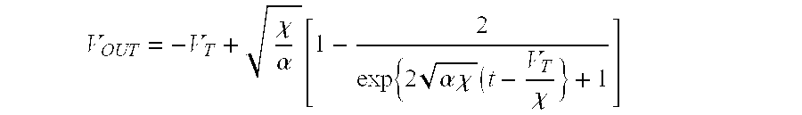
- The graphical representation is shown in FIG. 4.
- The method is capable of meeting several AMOLED specifications, namely:
- 1.) 6-bit to 8-bit accurate gray levels
- 2.) Independent gray level control for each color
- 3.) Precharge Cp to approximately T2 threshold voltage.
- 4.) Selectable current magnitude range from 10 nA to 100 uA per column with 6-bit to 8-bit control (100/64% to 100/256% accuracy)
- 5.) Output matching (Cp charging to T2 threshold voltage) to 1% adequate
- 6.) Row time current source settling.
- For example, letting Vdd=5V, Rs=50 KOhms, and the parasitic data line capacitance being 10 pF gives a charging time, γ, of 10 V/usec. This slew rate insures that the internal Opamp slew rates are higher, and that the feedback will respond quicker than the charging of the data line capacitance. To reach a T2 threshold voltage, Vt, of 5V would take approximately 500 nsec, where t0=500 nsec. For larger displays exhibiting larger data line capacitance, Rs can be reduced proportionally, with the lower limit being approximately the output resistance of the current driver, or for today's drivers, a reasonable output resistance of today's current data driver is approximately 2 Kohm per output
- A number of approaches have been made in solving the problem discussed here. For example, one approach (Clare Micronix) uses a column driver chip and circuit therein for reserving a constant time portion of the scan cycle to precharge the columns to a voltage threshold that is just below the onset of conduction. During a second time portion, the driver circuit applies a precision, but constant on current that is pulse width modulated to give an integrated current density proportional to the desired OLED light output.
- The disclosed approach differs substantially and has the advantages of (1) uses only one time portion (verus two), (2) using a nonlinear (versus constant) current amplitude, and (3) using current amplitude modulation (versus pulse width modulation). The advantages of (1), or of using only one time portion is that there is more time available for OLED luminance, and since the output luminance is proportional to the integrated current density over the frame cycle, a lower amplitude current is needed to achieve the same integrated current density. The OLED is more power efficient operating at lower current density. The advantage of (2), or using a nonlinear current amplitude is that precharge time is minimized and independent of colors. The data line capacitance to the pixel will vary dependent on the pixel location from the data current driver source, so minimizing the data line parasitic charging leaves more time for pixel capacitance charging, resulting in more accuracy. The advantage of (3), of using current amplitude modulation is that the entire scan time is available for OLED luminance, and as stated above, since the output luminance is proportional to the integrated current density over the frame cycle, a lower amplitude current is needed to achieve the same integrated current density, thus providing a more power efficient drive method.
- Table 1 shows the range of the nonlinear current source pixel feedback circuit for various parameters. The dependency of the parameter on the final pixel current, Ipixel, and charging time, t@0.999 Ipixel(t=α), as a dependency on the parameters can be obtained by comparing the different rows. This is only an example for illustrative purposes, where optimization has not been performed. For example, data rows 3 through 6 (blue) correspond to three orders of magnitude in pixel current, (Ipixzel from 10 nA to 10 uA) and the corresponding charging time to achieve 0.999 of the targeted pixel current (t@0.999 Ipixel(t=α) from 9.99 nA to 9.99 uA), or 0.1% error, which ranges from 0.6 usec to 0.9 usec.
Rows 7 through 10 (green) correspond to the four rows 3 through 6 (blue) with the threshold voltage of M2 in the pixel now shifted by 5V, from a Vt of 2V to a V5 of 7V, which now ranges from a charging time of 1.0 usec to 1.6 usec. If an even faster charging time is desired, Vdd may be increased, for example from 5V to 10V. Rows 13 through 16 correspond to theearlier rows - FIG. 5 a and 5 b show the dependency of the line capacitance over a range of 10 pF to 50 pF on the charge up time verus the pixel current and pixel voltage reference error, respectively. The three set of curves correspond to
rows 1 through 3 of Table 1. FIG. 6a and 6 b show the dependency of the pixel current over a range of 10 nA to 10 uA on the charge up time verus the pixel current and pixel voltage reference error, respectively, for a situation after a 5V TFT threshold voltage shift. The four sets of curves correspond to rows; 7 through 10 of Table 1.TABLE I Nonlinear Current Source Pixel Feedback (Sets of examples and data) −Vgs of T@0.99 T@0.999 Pixel TFT M2 Cs Rs Rd Vt of M2 Vdd M2 Iref Ipixel Ipixel Ipixel Turn on Time Row (pF) (Ohms) (Ohms) (V) (V) (V) (t = 0) (t = α) (t = α) (t = α) Constant τ0 1 10 50K 5 M 2 5 −2.3 100 uA 10 nA 0.3 usec 0.4 usec 0.2 usec 2 50 50K 5 M 2 5 −2.3 100 uA 10 nA 1.5 usec 1.6 usec 1.0 usec 3 20 50K 5 M 2 5 −2.3 100 uA 10 nA 0.6 usec 0.7 usec 0.4 usec 4 20 25K 500K 2 5 −2.96 200 uA 100 nA 0.5 usec 0.6 usec 0.2 usec 5 20 12.5K 50K 2 5 −5.05 400 uA 1 uA 0.6 usec 0.8 usec 0.1 usec 6 20 5K 5K 2 5 −11.67 1 mA 10 uA 0.6 usec 0.9 usec 0.04 usec 7 20 50K 5 M 7 5 −7.3 100 uA 10 nA 1.6 usec 1.6 usec 1.4 usec 8 20 25K 500K 7 5 −7.96 200 uA 100 nA 1.0 usec 1.1 usec 0.7 usec 9 20 12.5K 50K 7 5 −10.05 400 uA 1 uA 0.8 usec 1.0 usec 0.35 usec 10 20 5K 5K 7 5 −16.67 1 mA 10 uA 0.8 usec 1.0 usec 0.14 usec 11 20 50K 5 M 7 10 −7.43 200 uA 20 nA 0.8 usec 0.9 usec 0.7 usec 12 20 5K 5K 7 10 −20.68 2 mA 20 uA 0.5 usec 0.6 usec 0.07 usec 13 20 50K 10 M 7 10 −7.3 200 uA 10 nA 0.8 usec 0.9 usec 0.7 usec 14 20 5K 10K 7 10 −16.65 2 mA 10 uA 0.4 usec 0.5 usec 0.07 usec 15 20 50K 10 M 2 10 −2.3 200 uA 10 nA 0.3 usec 0.4 usec 0.2 usec 16 20 5K 10K 2 10 −11.65 2 mA 10 uA 0.3 usec 0.4 usec 0.02 usec - The invention having been thus described with particular reference to the preferred forms thereof, it will be obvious that various changes and modifications may be made therein without departing from the spirit and scope of the invention as defined in the appended claims.
Claims (6)
1. A light emitting pixel circuit comprising a light emitting diode having a parasitic capacitance and coupled to a current source; nonlinear feedback means for rapidly charging the parasitic capacitance and for enabling, immediately following such charging, illumination of the diode responsive to a predefined constant current level from the current source.
2. A light emitting pixel circuit wherein said current source is voltage controlled by operation of the feedback means.
3. A light emitting pixel circuit including means for controlling the charging time.
4. A light emitting pixel circuit, wherein the feedback means include current sense means.
5. A light emitting pixel circuit as defined in claim 4 , wherein the current sense means includes two interconnected operational amplifiers.
6. A light emitting pixel circuit as defined in claim 5 , wherein the current source includes two interconnected operational amplifiers.
Priority Applications (1)
| Application Number | Priority Date | Filing Date | Title |
|---|---|---|---|
| US10/300,640 US20040095297A1 (en) | 2002-11-20 | 2002-11-20 | Nonlinear voltage controlled current source with feedback circuit |
Applications Claiming Priority (1)
| Application Number | Priority Date | Filing Date | Title |
|---|---|---|---|
| US10/300,640 US20040095297A1 (en) | 2002-11-20 | 2002-11-20 | Nonlinear voltage controlled current source with feedback circuit |
Publications (1)
| Publication Number | Publication Date |
|---|---|
| US20040095297A1 true US20040095297A1 (en) | 2004-05-20 |
Family
ID=32297943
Family Applications (1)
| Application Number | Title | Priority Date | Filing Date |
|---|---|---|---|
| US10/300,640 Abandoned US20040095297A1 (en) | 2002-11-20 | 2002-11-20 | Nonlinear voltage controlled current source with feedback circuit |
Country Status (1)
| Country | Link |
|---|---|
| US (1) | US20040095297A1 (en) |
Cited By (71)
| Publication number | Priority date | Publication date | Assignee | Title |
|---|---|---|---|---|
| US20040222954A1 (en) * | 2003-04-07 | 2004-11-11 | Lueder Ernst H. | Methods and apparatus for a display |
| US20050068275A1 (en) * | 2003-09-29 | 2005-03-31 | Kane Michael Gillis | Driver circuit, as for an OLED display |
| US20060208961A1 (en) * | 2005-02-10 | 2006-09-21 | Arokia Nathan | Driving circuit for current programmed organic light-emitting diode displays |
| US20070024541A1 (en) * | 2005-08-01 | 2007-02-01 | Ryu Do H | Organic light emitting display |
| WO2007120474A2 (en) * | 2006-04-10 | 2007-10-25 | Emagin Corporation | Auto-calibrating gamma correction circuit for amoled pixel display drive |
| US20080055223A1 (en) * | 2006-06-16 | 2008-03-06 | Roger Stewart | Pixel circuits and methods for driving pixels |
| US20080062090A1 (en) * | 2006-06-16 | 2008-03-13 | Roger Stewart | Pixel circuits and methods for driving pixels |
| US20080062091A1 (en) * | 2006-06-16 | 2008-03-13 | Roger Stewart | Pixel circuits and methods for driving pixels |
| US20080297452A1 (en) * | 2007-05-30 | 2008-12-04 | Honeywell International, Inc. | Apparatus, systems, and methods for dimming an active matrix light-emitting diode (LED) display |
| US20090115704A1 (en) * | 2003-09-29 | 2009-05-07 | Michael Gillis Kane | Pixel circuit for an active matrix organic light-emitting diode display |
| US20110191042A1 (en) * | 2010-02-04 | 2011-08-04 | Ignis Innovation Inc. | System and methods for extracting correlation curves for an organic light emitting device |
| EP2431964A1 (en) * | 2009-05-13 | 2012-03-21 | Sharp Kabushiki Kaisha | Display apparatus |
| USRE44563E1 (en) * | 2005-10-07 | 2013-10-29 | Sony Corporation | Pixel circuit and display apparatus |
| US20140125713A1 (en) * | 2005-08-10 | 2014-05-08 | IUCF-HYU (Industry-University Corporation Foundation Hanyang University) | Data driver, organic light emitting display device using the same, and method of driving the organic light emitting display device |
| US8743096B2 (en) | 2006-04-19 | 2014-06-03 | Ignis Innovation, Inc. | Stable driving scheme for active matrix displays |
| US8816946B2 (en) | 2004-12-15 | 2014-08-26 | Ignis Innovation Inc. | Method and system for programming, calibrating and driving a light emitting device display |
| US8907991B2 (en) | 2010-12-02 | 2014-12-09 | Ignis Innovation Inc. | System and methods for thermal compensation in AMOLED displays |
| USRE45291E1 (en) | 2004-06-29 | 2014-12-16 | Ignis Innovation Inc. | Voltage-programming scheme for current-driven AMOLED displays |
| US8922544B2 (en) | 2012-05-23 | 2014-12-30 | Ignis Innovation Inc. | Display systems with compensation for line propagation delay |
| US8941697B2 (en) | 2003-09-23 | 2015-01-27 | Ignis Innovation Inc. | Circuit and method for driving an array of light emitting pixels |
| US8994617B2 (en) | 2010-03-17 | 2015-03-31 | Ignis Innovation Inc. | Lifetime uniformity parameter extraction methods |
| US9059117B2 (en) | 2009-12-01 | 2015-06-16 | Ignis Innovation Inc. | High resolution pixel architecture |
| WO2015100422A1 (en) * | 2013-12-27 | 2015-07-02 | University Of Washington Through Its Center For Commercialization | Adaptive control of a fiber scanner with piezoelectric sensing |
| US9093029B2 (en) | 2011-05-20 | 2015-07-28 | Ignis Innovation Inc. | System and methods for extraction of threshold and mobility parameters in AMOLED displays |
| US9093028B2 (en) | 2009-12-06 | 2015-07-28 | Ignis Innovation Inc. | System and methods for power conservation for AMOLED pixel drivers |
| US9111485B2 (en) | 2009-06-16 | 2015-08-18 | Ignis Innovation Inc. | Compensation technique for color shift in displays |
| US9125278B2 (en) | 2006-08-15 | 2015-09-01 | Ignis Innovation Inc. | OLED luminance degradation compensation |
| US9171504B2 (en) | 2013-01-14 | 2015-10-27 | Ignis Innovation Inc. | Driving scheme for emissive displays providing compensation for driving transistor variations |
| US9171500B2 (en) | 2011-05-20 | 2015-10-27 | Ignis Innovation Inc. | System and methods for extraction of parasitic parameters in AMOLED displays |
| US20150379909A1 (en) * | 2014-06-27 | 2015-12-31 | Lg Display Co., Ltd. | Organic light emitting display for sensing electrical characteristics of driving element |
| US9275579B2 (en) | 2004-12-15 | 2016-03-01 | Ignis Innovation Inc. | System and methods for extraction of threshold and mobility parameters in AMOLED displays |
| US9280933B2 (en) | 2004-12-15 | 2016-03-08 | Ignis Innovation Inc. | System and methods for extraction of threshold and mobility parameters in AMOLED displays |
| US9305488B2 (en) | 2013-03-14 | 2016-04-05 | Ignis Innovation Inc. | Re-interpolation with edge detection for extracting an aging pattern for AMOLED displays |
| US9311859B2 (en) | 2009-11-30 | 2016-04-12 | Ignis Innovation Inc. | Resetting cycle for aging compensation in AMOLED displays |
| US9324268B2 (en) | 2013-03-15 | 2016-04-26 | Ignis Innovation Inc. | Amoled displays with multiple readout circuits |
| US9336717B2 (en) | 2012-12-11 | 2016-05-10 | Ignis Innovation Inc. | Pixel circuits for AMOLED displays |
| US9343006B2 (en) | 2012-02-03 | 2016-05-17 | Ignis Innovation Inc. | Driving system for active-matrix displays |
| US9384698B2 (en) | 2009-11-30 | 2016-07-05 | Ignis Innovation Inc. | System and methods for aging compensation in AMOLED displays |
| US9437137B2 (en) | 2013-08-12 | 2016-09-06 | Ignis Innovation Inc. | Compensation accuracy |
| US9466240B2 (en) | 2011-05-26 | 2016-10-11 | Ignis Innovation Inc. | Adaptive feedback system for compensating for aging pixel areas with enhanced estimation speed |
| US9530349B2 (en) | 2011-05-20 | 2016-12-27 | Ignis Innovations Inc. | Charged-based compensation and parameter extraction in AMOLED displays |
| US9741282B2 (en) | 2013-12-06 | 2017-08-22 | Ignis Innovation Inc. | OLED display system and method |
| US9747834B2 (en) | 2012-05-11 | 2017-08-29 | Ignis Innovation Inc. | Pixel circuits including feedback capacitors and reset capacitors, and display systems therefore |
| US9761170B2 (en) | 2013-12-06 | 2017-09-12 | Ignis Innovation Inc. | Correction for localized phenomena in an image array |
| US9773439B2 (en) | 2011-05-27 | 2017-09-26 | Ignis Innovation Inc. | Systems and methods for aging compensation in AMOLED displays |
| US9786209B2 (en) | 2009-11-30 | 2017-10-10 | Ignis Innovation Inc. | System and methods for aging compensation in AMOLED displays |
| US9786223B2 (en) | 2012-12-11 | 2017-10-10 | Ignis Innovation Inc. | Pixel circuits for AMOLED displays |
| US9799246B2 (en) | 2011-05-20 | 2017-10-24 | Ignis Innovation Inc. | System and methods for extraction of threshold and mobility parameters in AMOLED displays |
| US9830857B2 (en) | 2013-01-14 | 2017-11-28 | Ignis Innovation Inc. | Cleaning common unwanted signals from pixel measurements in emissive displays |
| US9881532B2 (en) | 2010-02-04 | 2018-01-30 | Ignis Innovation Inc. | System and method for extracting correlation curves for an organic light emitting device |
| US9947293B2 (en) | 2015-05-27 | 2018-04-17 | Ignis Innovation Inc. | Systems and methods of reduced memory bandwidth compensation |
| US10013907B2 (en) | 2004-12-15 | 2018-07-03 | Ignis Innovation Inc. | Method and system for programming, calibrating and/or compensating, and driving an LED display |
| US10012678B2 (en) | 2004-12-15 | 2018-07-03 | Ignis Innovation Inc. | Method and system for programming, calibrating and/or compensating, and driving an LED display |
| US10019941B2 (en) | 2005-09-13 | 2018-07-10 | Ignis Innovation Inc. | Compensation technique for luminance degradation in electro-luminance devices |
| US10074304B2 (en) | 2015-08-07 | 2018-09-11 | Ignis Innovation Inc. | Systems and methods of pixel calibration based on improved reference values |
| US10089924B2 (en) | 2011-11-29 | 2018-10-02 | Ignis Innovation Inc. | Structural and low-frequency non-uniformity compensation |
| US10089921B2 (en) | 2010-02-04 | 2018-10-02 | Ignis Innovation Inc. | System and methods for extracting correlation curves for an organic light emitting device |
| US10163401B2 (en) | 2010-02-04 | 2018-12-25 | Ignis Innovation Inc. | System and methods for extracting correlation curves for an organic light emitting device |
| US10176736B2 (en) | 2010-02-04 | 2019-01-08 | Ignis Innovation Inc. | System and methods for extracting correlation curves for an organic light emitting device |
| US10181282B2 (en) | 2015-01-23 | 2019-01-15 | Ignis Innovation Inc. | Compensation for color variations in emissive devices |
| US10192479B2 (en) | 2014-04-08 | 2019-01-29 | Ignis Innovation Inc. | Display system using system level resources to calculate compensation parameters for a display module in a portable device |
| US10235933B2 (en) | 2005-04-12 | 2019-03-19 | Ignis Innovation Inc. | System and method for compensation of non-uniformities in light emitting device displays |
| US10311780B2 (en) | 2015-05-04 | 2019-06-04 | Ignis Innovation Inc. | Systems and methods of optical feedback |
| US10319307B2 (en) | 2009-06-16 | 2019-06-11 | Ignis Innovation Inc. | Display system with compensation techniques and/or shared level resources |
| US10388221B2 (en) | 2005-06-08 | 2019-08-20 | Ignis Innovation Inc. | Method and system for driving a light emitting device display |
| US10439159B2 (en) | 2013-12-25 | 2019-10-08 | Ignis Innovation Inc. | Electrode contacts |
| US10573231B2 (en) | 2010-02-04 | 2020-02-25 | Ignis Innovation Inc. | System and methods for extracting correlation curves for an organic light emitting device |
| WO2020099102A1 (en) * | 2018-11-16 | 2020-05-22 | Osram Opto Semiconductors Gmbh | Optoelectronic lighting device and method for controlling an optoelectronic lighting device |
| CN111583864A (en) * | 2020-06-11 | 2020-08-25 | 京东方科技集团股份有限公司 | Display driving circuit, driving method thereof and display device |
| US10867536B2 (en) | 2013-04-22 | 2020-12-15 | Ignis Innovation Inc. | Inspection system for OLED display panels |
| US10996258B2 (en) | 2009-11-30 | 2021-05-04 | Ignis Innovation Inc. | Defect detection and correction of pixel circuits for AMOLED displays |
Citations (21)
| Publication number | Priority date | Publication date | Assignee | Title |
|---|---|---|---|---|
| US5049855A (en) * | 1989-10-24 | 1991-09-17 | Slemon Charles S | Security screen system |
| US5173685A (en) * | 1988-10-14 | 1992-12-22 | Gordon Alan King | Monitoring circuits for lamps or other electrical loads using a comparator with a constant voltage power supply |
| US5347144A (en) * | 1990-07-04 | 1994-09-13 | Centre National De La Recherche Scientifique (Cnrs) | Thin-layer field-effect transistors with MIS structure whose insulator and semiconductor are made of organic materials |
| US5552678A (en) * | 1994-09-23 | 1996-09-03 | Eastman Kodak Company | AC drive scheme for organic led |
| US5771286A (en) * | 1994-08-31 | 1998-06-23 | Sgs-Thomson Microelectronics Pte Ltd | Speech amplifier associated with an LED |
| US5788789A (en) * | 1995-06-08 | 1998-08-04 | George Fischer Sloane, Inc. | Power device for fusing plastic pipe joints |
| US5903247A (en) * | 1996-07-19 | 1999-05-11 | The Regents Of The University Of California | Servo controlled liquid crystal windows |
| US5910792A (en) * | 1997-11-12 | 1999-06-08 | Candescent Technologies, Corp. | Method and apparatus for brightness control in a field emission display |
| US5952789A (en) * | 1997-04-14 | 1999-09-14 | Sarnoff Corporation | Active matrix organic light emitting diode (amoled) display pixel structure and data load/illuminate circuit therefor |
| US6023259A (en) * | 1997-07-11 | 2000-02-08 | Fed Corporation | OLED active matrix using a single transistor current mode pixel design |
| US6229508B1 (en) * | 1997-09-29 | 2001-05-08 | Sarnoff Corporation | Active matrix light emitting diode pixel structure and concomitant method |
| US6229506B1 (en) * | 1997-04-23 | 2001-05-08 | Sarnoff Corporation | Active matrix light emitting diode pixel structure and concomitant method |
| US20020030455A1 (en) * | 1999-12-23 | 2002-03-14 | Gelcore, Llc | Non-linear light-emitting load current control |
| US6420056B1 (en) * | 1999-07-08 | 2002-07-16 | International Business Machines Corporation | Electroluminescent device with dye-containing organic-inorganic hybrid materials as an emitting layer |
| US6433488B1 (en) * | 2001-01-02 | 2002-08-13 | Chi Mei Optoelectronics Corp. | OLED active driving system with current feedback |
| US6452576B1 (en) * | 1999-01-21 | 2002-09-17 | Koninklijke Philips Electronics N.V. | Organic electroluminescent display device |
| US6621259B2 (en) * | 2001-05-30 | 2003-09-16 | Texas Instruments Incorporated | Current sense amplifier and method |
| US6691239B1 (en) * | 2000-11-13 | 2004-02-10 | Intel Corporation | Voltage sequencing circuit |
| US6693388B2 (en) * | 2001-07-27 | 2004-02-17 | Canon Kabushiki Kaisha | Active matrix display |
| US6771679B2 (en) * | 2000-05-17 | 2004-08-03 | David Chalmers Schie | Apparatus and method for programmable control of laser diode modulation and operating point |
| US6806857B2 (en) * | 2000-05-22 | 2004-10-19 | Koninklijke Philips Electronics N.V. | Display device |
-
2002
- 2002-11-20 US US10/300,640 patent/US20040095297A1/en not_active Abandoned
Patent Citations (21)
| Publication number | Priority date | Publication date | Assignee | Title |
|---|---|---|---|---|
| US5173685A (en) * | 1988-10-14 | 1992-12-22 | Gordon Alan King | Monitoring circuits for lamps or other electrical loads using a comparator with a constant voltage power supply |
| US5049855A (en) * | 1989-10-24 | 1991-09-17 | Slemon Charles S | Security screen system |
| US5347144A (en) * | 1990-07-04 | 1994-09-13 | Centre National De La Recherche Scientifique (Cnrs) | Thin-layer field-effect transistors with MIS structure whose insulator and semiconductor are made of organic materials |
| US5771286A (en) * | 1994-08-31 | 1998-06-23 | Sgs-Thomson Microelectronics Pte Ltd | Speech amplifier associated with an LED |
| US5552678A (en) * | 1994-09-23 | 1996-09-03 | Eastman Kodak Company | AC drive scheme for organic led |
| US5788789A (en) * | 1995-06-08 | 1998-08-04 | George Fischer Sloane, Inc. | Power device for fusing plastic pipe joints |
| US5903247A (en) * | 1996-07-19 | 1999-05-11 | The Regents Of The University Of California | Servo controlled liquid crystal windows |
| US5952789A (en) * | 1997-04-14 | 1999-09-14 | Sarnoff Corporation | Active matrix organic light emitting diode (amoled) display pixel structure and data load/illuminate circuit therefor |
| US6229506B1 (en) * | 1997-04-23 | 2001-05-08 | Sarnoff Corporation | Active matrix light emitting diode pixel structure and concomitant method |
| US6023259A (en) * | 1997-07-11 | 2000-02-08 | Fed Corporation | OLED active matrix using a single transistor current mode pixel design |
| US6229508B1 (en) * | 1997-09-29 | 2001-05-08 | Sarnoff Corporation | Active matrix light emitting diode pixel structure and concomitant method |
| US5910792A (en) * | 1997-11-12 | 1999-06-08 | Candescent Technologies, Corp. | Method and apparatus for brightness control in a field emission display |
| US6452576B1 (en) * | 1999-01-21 | 2002-09-17 | Koninklijke Philips Electronics N.V. | Organic electroluminescent display device |
| US6420056B1 (en) * | 1999-07-08 | 2002-07-16 | International Business Machines Corporation | Electroluminescent device with dye-containing organic-inorganic hybrid materials as an emitting layer |
| US20020030455A1 (en) * | 1999-12-23 | 2002-03-14 | Gelcore, Llc | Non-linear light-emitting load current control |
| US6771679B2 (en) * | 2000-05-17 | 2004-08-03 | David Chalmers Schie | Apparatus and method for programmable control of laser diode modulation and operating point |
| US6806857B2 (en) * | 2000-05-22 | 2004-10-19 | Koninklijke Philips Electronics N.V. | Display device |
| US6691239B1 (en) * | 2000-11-13 | 2004-02-10 | Intel Corporation | Voltage sequencing circuit |
| US6433488B1 (en) * | 2001-01-02 | 2002-08-13 | Chi Mei Optoelectronics Corp. | OLED active driving system with current feedback |
| US6621259B2 (en) * | 2001-05-30 | 2003-09-16 | Texas Instruments Incorporated | Current sense amplifier and method |
| US6693388B2 (en) * | 2001-07-27 | 2004-02-17 | Canon Kabushiki Kaisha | Active matrix display |
Cited By (162)
| Publication number | Priority date | Publication date | Assignee | Title |
|---|---|---|---|---|
| US20050128193A1 (en) * | 2003-04-07 | 2005-06-16 | Lueder Ernst H. | Methods and apparatus for a display |
| US20040222954A1 (en) * | 2003-04-07 | 2004-11-11 | Lueder Ernst H. | Methods and apparatus for a display |
| US9852689B2 (en) | 2003-09-23 | 2017-12-26 | Ignis Innovation Inc. | Circuit and method for driving an array of light emitting pixels |
| US8941697B2 (en) | 2003-09-23 | 2015-01-27 | Ignis Innovation Inc. | Circuit and method for driving an array of light emitting pixels |
| US10089929B2 (en) | 2003-09-23 | 2018-10-02 | Ignis Innovation Inc. | Pixel driver circuit with load-balance in current mirror circuit |
| US9472138B2 (en) | 2003-09-23 | 2016-10-18 | Ignis Innovation Inc. | Pixel driver circuit with load-balance in current mirror circuit |
| US9472139B2 (en) | 2003-09-23 | 2016-10-18 | Ignis Innovation Inc. | Circuit and method for driving an array of light emitting pixels |
| US7633470B2 (en) * | 2003-09-29 | 2009-12-15 | Michael Gillis Kane | Driver circuit, as for an OLED display |
| US20090115704A1 (en) * | 2003-09-29 | 2009-05-07 | Michael Gillis Kane | Pixel circuit for an active matrix organic light-emitting diode display |
| US20050068275A1 (en) * | 2003-09-29 | 2005-03-31 | Kane Michael Gillis | Driver circuit, as for an OLED display |
| US7956825B2 (en) | 2003-09-29 | 2011-06-07 | Transpacific Infinity, Llc | Pixel circuit for an active matrix organic light-emitting diode display |
| USRE47257E1 (en) | 2004-06-29 | 2019-02-26 | Ignis Innovation Inc. | Voltage-programming scheme for current-driven AMOLED displays |
| USRE45291E1 (en) | 2004-06-29 | 2014-12-16 | Ignis Innovation Inc. | Voltage-programming scheme for current-driven AMOLED displays |
| US9280933B2 (en) | 2004-12-15 | 2016-03-08 | Ignis Innovation Inc. | System and methods for extraction of threshold and mobility parameters in AMOLED displays |
| US10013907B2 (en) | 2004-12-15 | 2018-07-03 | Ignis Innovation Inc. | Method and system for programming, calibrating and/or compensating, and driving an LED display |
| US9970964B2 (en) | 2004-12-15 | 2018-05-15 | Ignis Innovation Inc. | Method and system for programming, calibrating and driving a light emitting device display |
| US10012678B2 (en) | 2004-12-15 | 2018-07-03 | Ignis Innovation Inc. | Method and system for programming, calibrating and/or compensating, and driving an LED display |
| US8816946B2 (en) | 2004-12-15 | 2014-08-26 | Ignis Innovation Inc. | Method and system for programming, calibrating and driving a light emitting device display |
| US9275579B2 (en) | 2004-12-15 | 2016-03-01 | Ignis Innovation Inc. | System and methods for extraction of threshold and mobility parameters in AMOLED displays |
| US10699624B2 (en) | 2004-12-15 | 2020-06-30 | Ignis Innovation Inc. | Method and system for programming, calibrating and/or compensating, and driving an LED display |
| US8994625B2 (en) | 2004-12-15 | 2015-03-31 | Ignis Innovation Inc. | Method and system for programming, calibrating and driving a light emitting device display |
| US20060208961A1 (en) * | 2005-02-10 | 2006-09-21 | Arokia Nathan | Driving circuit for current programmed organic light-emitting diode displays |
| TWI409750B (en) * | 2005-02-10 | 2013-09-21 | Ignis Innovation Inc | Driving circuit for current programmed organic light-emitting diode displays |
| US10078984B2 (en) * | 2005-02-10 | 2018-09-18 | Ignis Innovation Inc. | Driving circuit for current programmed organic light-emitting diode displays |
| US10235933B2 (en) | 2005-04-12 | 2019-03-19 | Ignis Innovation Inc. | System and method for compensation of non-uniformities in light emitting device displays |
| US10388221B2 (en) | 2005-06-08 | 2019-08-20 | Ignis Innovation Inc. | Method and system for driving a light emitting device display |
| US8593378B2 (en) * | 2005-08-01 | 2013-11-26 | Samsung Display Co., Ltd. | Organic light emitting display |
| US20070024541A1 (en) * | 2005-08-01 | 2007-02-01 | Ryu Do H | Organic light emitting display |
| US20140125713A1 (en) * | 2005-08-10 | 2014-05-08 | IUCF-HYU (Industry-University Corporation Foundation Hanyang University) | Data driver, organic light emitting display device using the same, and method of driving the organic light emitting display device |
| US10192491B2 (en) | 2005-08-10 | 2019-01-29 | Samsung Display Co., Ltd. | Data driver, organic light emitting display device using the same, and method of driving the organic light emitting display device |
| US9812065B2 (en) * | 2005-08-10 | 2017-11-07 | Samsung Display Co., Ltd. | Data driver, organic light emitting display device using the same, and method of driving the organic light emitting display device |
| US10019941B2 (en) | 2005-09-13 | 2018-07-10 | Ignis Innovation Inc. | Compensation technique for luminance degradation in electro-luminance devices |
| USRE45400E1 (en) | 2005-10-07 | 2015-03-03 | Sony Corporation | Pixel circuit and display apparatus |
| USRE44563E1 (en) * | 2005-10-07 | 2013-10-29 | Sony Corporation | Pixel circuit and display apparatus |
| WO2007120474A2 (en) * | 2006-04-10 | 2007-10-25 | Emagin Corporation | Auto-calibrating gamma correction circuit for amoled pixel display drive |
| WO2007120474A3 (en) * | 2006-04-10 | 2008-04-24 | Emagin Corp | Auto-calibrating gamma correction circuit for amoled pixel display drive |
| US8743096B2 (en) | 2006-04-19 | 2014-06-03 | Ignis Innovation, Inc. | Stable driving scheme for active matrix displays |
| US9842544B2 (en) | 2006-04-19 | 2017-12-12 | Ignis Innovation Inc. | Stable driving scheme for active matrix displays |
| US10453397B2 (en) | 2006-04-19 | 2019-10-22 | Ignis Innovation Inc. | Stable driving scheme for active matrix displays |
| US9633597B2 (en) | 2006-04-19 | 2017-04-25 | Ignis Innovation Inc. | Stable driving scheme for active matrix displays |
| US10127860B2 (en) | 2006-04-19 | 2018-11-13 | Ignis Innovation Inc. | Stable driving scheme for active matrix displays |
| US7679586B2 (en) | 2006-06-16 | 2010-03-16 | Roger Green Stewart | Pixel circuits and methods for driving pixels |
| US8531359B2 (en) | 2006-06-16 | 2013-09-10 | Visam Development L.L.C. | Pixel circuits and methods for driving pixels |
| US8446394B2 (en) | 2006-06-16 | 2013-05-21 | Visam Development L.L.C. | Pixel circuits and methods for driving pixels |
| US20080055223A1 (en) * | 2006-06-16 | 2008-03-06 | Roger Stewart | Pixel circuits and methods for driving pixels |
| US20080062091A1 (en) * | 2006-06-16 | 2008-03-13 | Roger Stewart | Pixel circuits and methods for driving pixels |
| US8937582B2 (en) | 2006-06-16 | 2015-01-20 | Visam Development L.L.C. | Pixel circuit display driver |
| US20080062090A1 (en) * | 2006-06-16 | 2008-03-13 | Roger Stewart | Pixel circuits and methods for driving pixels |
| US9530352B2 (en) | 2006-08-15 | 2016-12-27 | Ignis Innovations Inc. | OLED luminance degradation compensation |
| US9125278B2 (en) | 2006-08-15 | 2015-09-01 | Ignis Innovation Inc. | OLED luminance degradation compensation |
| US10325554B2 (en) | 2006-08-15 | 2019-06-18 | Ignis Innovation Inc. | OLED luminance degradation compensation |
| US20080297452A1 (en) * | 2007-05-30 | 2008-12-04 | Honeywell International, Inc. | Apparatus, systems, and methods for dimming an active matrix light-emitting diode (LED) display |
| US7956831B2 (en) * | 2007-05-30 | 2011-06-07 | Honeywell Interntional Inc. | Apparatus, systems, and methods for dimming an active matrix light-emitting diode (LED) display |
| EP2431964A1 (en) * | 2009-05-13 | 2012-03-21 | Sharp Kabushiki Kaisha | Display apparatus |
| EP2431964A4 (en) * | 2009-05-13 | 2013-04-10 | Sharp Kk | Display apparatus |
| US9111485B2 (en) | 2009-06-16 | 2015-08-18 | Ignis Innovation Inc. | Compensation technique for color shift in displays |
| US9418587B2 (en) | 2009-06-16 | 2016-08-16 | Ignis Innovation Inc. | Compensation technique for color shift in displays |
| US9117400B2 (en) | 2009-06-16 | 2015-08-25 | Ignis Innovation Inc. | Compensation technique for color shift in displays |
| US10553141B2 (en) | 2009-06-16 | 2020-02-04 | Ignis Innovation Inc. | Compensation technique for color shift in displays |
| US10319307B2 (en) | 2009-06-16 | 2019-06-11 | Ignis Innovation Inc. | Display system with compensation techniques and/or shared level resources |
| US9786209B2 (en) | 2009-11-30 | 2017-10-10 | Ignis Innovation Inc. | System and methods for aging compensation in AMOLED displays |
| US9384698B2 (en) | 2009-11-30 | 2016-07-05 | Ignis Innovation Inc. | System and methods for aging compensation in AMOLED displays |
| US10996258B2 (en) | 2009-11-30 | 2021-05-04 | Ignis Innovation Inc. | Defect detection and correction of pixel circuits for AMOLED displays |
| US10679533B2 (en) | 2009-11-30 | 2020-06-09 | Ignis Innovation Inc. | System and methods for aging compensation in AMOLED displays |
| US9311859B2 (en) | 2009-11-30 | 2016-04-12 | Ignis Innovation Inc. | Resetting cycle for aging compensation in AMOLED displays |
| US10699613B2 (en) | 2009-11-30 | 2020-06-30 | Ignis Innovation Inc. | Resetting cycle for aging compensation in AMOLED displays |
| US10304390B2 (en) | 2009-11-30 | 2019-05-28 | Ignis Innovation Inc. | System and methods for aging compensation in AMOLED displays |
| US9059117B2 (en) | 2009-12-01 | 2015-06-16 | Ignis Innovation Inc. | High resolution pixel architecture |
| US9093028B2 (en) | 2009-12-06 | 2015-07-28 | Ignis Innovation Inc. | System and methods for power conservation for AMOLED pixel drivers |
| US9262965B2 (en) | 2009-12-06 | 2016-02-16 | Ignis Innovation Inc. | System and methods for power conservation for AMOLED pixel drivers |
| US9773441B2 (en) | 2010-02-04 | 2017-09-26 | Ignis Innovation Inc. | System and methods for extracting correlation curves for an organic light emitting device |
| US10032399B2 (en) | 2010-02-04 | 2018-07-24 | Ignis Innovation Inc. | System and methods for extracting correlation curves for an organic light emitting device |
| US9430958B2 (en) | 2010-02-04 | 2016-08-30 | Ignis Innovation Inc. | System and methods for extracting correlation curves for an organic light emitting device |
| US11200839B2 (en) | 2010-02-04 | 2021-12-14 | Ignis Innovation Inc. | System and methods for extracting correlation curves for an organic light emitting device |
| US20110191042A1 (en) * | 2010-02-04 | 2011-08-04 | Ignis Innovation Inc. | System and methods for extracting correlation curves for an organic light emitting device |
| US10971043B2 (en) | 2010-02-04 | 2021-04-06 | Ignis Innovation Inc. | System and method for extracting correlation curves for an organic light emitting device |
| US10089921B2 (en) | 2010-02-04 | 2018-10-02 | Ignis Innovation Inc. | System and methods for extracting correlation curves for an organic light emitting device |
| US8589100B2 (en) | 2010-02-04 | 2013-11-19 | Ignis Innovation Inc. | System and methods for extracting correlation curves for an organic light emitting device |
| US10395574B2 (en) | 2010-02-04 | 2019-08-27 | Ignis Innovation Inc. | System and methods for extracting correlation curves for an organic light emitting device |
| US9881532B2 (en) | 2010-02-04 | 2018-01-30 | Ignis Innovation Inc. | System and method for extracting correlation curves for an organic light emitting device |
| US10573231B2 (en) | 2010-02-04 | 2020-02-25 | Ignis Innovation Inc. | System and methods for extracting correlation curves for an organic light emitting device |
| US10176736B2 (en) | 2010-02-04 | 2019-01-08 | Ignis Innovation Inc. | System and methods for extracting correlation curves for an organic light emitting device |
| US10163401B2 (en) | 2010-02-04 | 2018-12-25 | Ignis Innovation Inc. | System and methods for extracting correlation curves for an organic light emitting device |
| US8994617B2 (en) | 2010-03-17 | 2015-03-31 | Ignis Innovation Inc. | Lifetime uniformity parameter extraction methods |
| US10460669B2 (en) | 2010-12-02 | 2019-10-29 | Ignis Innovation Inc. | System and methods for thermal compensation in AMOLED displays |
| US9997110B2 (en) | 2010-12-02 | 2018-06-12 | Ignis Innovation Inc. | System and methods for thermal compensation in AMOLED displays |
| US9489897B2 (en) | 2010-12-02 | 2016-11-08 | Ignis Innovation Inc. | System and methods for thermal compensation in AMOLED displays |
| US8907991B2 (en) | 2010-12-02 | 2014-12-09 | Ignis Innovation Inc. | System and methods for thermal compensation in AMOLED displays |
| US10580337B2 (en) | 2011-05-20 | 2020-03-03 | Ignis Innovation Inc. | System and methods for extraction of threshold and mobility parameters in AMOLED displays |
| US10127846B2 (en) | 2011-05-20 | 2018-11-13 | Ignis Innovation Inc. | System and methods for extraction of threshold and mobility parameters in AMOLED displays |
| US9093029B2 (en) | 2011-05-20 | 2015-07-28 | Ignis Innovation Inc. | System and methods for extraction of threshold and mobility parameters in AMOLED displays |
| US10325537B2 (en) | 2011-05-20 | 2019-06-18 | Ignis Innovation Inc. | System and methods for extraction of threshold and mobility parameters in AMOLED displays |
| US9589490B2 (en) | 2011-05-20 | 2017-03-07 | Ignis Innovation Inc. | System and methods for extraction of threshold and mobility parameters in AMOLED displays |
| US9171500B2 (en) | 2011-05-20 | 2015-10-27 | Ignis Innovation Inc. | System and methods for extraction of parasitic parameters in AMOLED displays |
| US9799248B2 (en) | 2011-05-20 | 2017-10-24 | Ignis Innovation Inc. | System and methods for extraction of threshold and mobility parameters in AMOLED displays |
| US10032400B2 (en) | 2011-05-20 | 2018-07-24 | Ignis Innovation Inc. | System and methods for extraction of threshold and mobility parameters in AMOLED displays |
| US9355584B2 (en) | 2011-05-20 | 2016-05-31 | Ignis Innovation Inc. | System and methods for extraction of threshold and mobility parameters in AMOLED displays |
| US9799246B2 (en) | 2011-05-20 | 2017-10-24 | Ignis Innovation Inc. | System and methods for extraction of threshold and mobility parameters in AMOLED displays |
| US9530349B2 (en) | 2011-05-20 | 2016-12-27 | Ignis Innovations Inc. | Charged-based compensation and parameter extraction in AMOLED displays |
| US10475379B2 (en) | 2011-05-20 | 2019-11-12 | Ignis Innovation Inc. | Charged-based compensation and parameter extraction in AMOLED displays |
| US10706754B2 (en) | 2011-05-26 | 2020-07-07 | Ignis Innovation Inc. | Adaptive feedback system for compensating for aging pixel areas with enhanced estimation speed |
| US9978297B2 (en) | 2011-05-26 | 2018-05-22 | Ignis Innovation Inc. | Adaptive feedback system for compensating for aging pixel areas with enhanced estimation speed |
| US9640112B2 (en) | 2011-05-26 | 2017-05-02 | Ignis Innovation Inc. | Adaptive feedback system for compensating for aging pixel areas with enhanced estimation speed |
| US9466240B2 (en) | 2011-05-26 | 2016-10-11 | Ignis Innovation Inc. | Adaptive feedback system for compensating for aging pixel areas with enhanced estimation speed |
| US10417945B2 (en) | 2011-05-27 | 2019-09-17 | Ignis Innovation Inc. | Systems and methods for aging compensation in AMOLED displays |
| US9984607B2 (en) | 2011-05-27 | 2018-05-29 | Ignis Innovation Inc. | Systems and methods for aging compensation in AMOLED displays |
| US9773439B2 (en) | 2011-05-27 | 2017-09-26 | Ignis Innovation Inc. | Systems and methods for aging compensation in AMOLED displays |
| US10380944B2 (en) | 2011-11-29 | 2019-08-13 | Ignis Innovation Inc. | Structural and low-frequency non-uniformity compensation |
| US10089924B2 (en) | 2011-11-29 | 2018-10-02 | Ignis Innovation Inc. | Structural and low-frequency non-uniformity compensation |
| US10043448B2 (en) | 2012-02-03 | 2018-08-07 | Ignis Innovation Inc. | Driving system for active-matrix displays |
| US10453394B2 (en) | 2012-02-03 | 2019-10-22 | Ignis Innovation Inc. | Driving system for active-matrix displays |
| US9792857B2 (en) | 2012-02-03 | 2017-10-17 | Ignis Innovation Inc. | Driving system for active-matrix displays |
| US9343006B2 (en) | 2012-02-03 | 2016-05-17 | Ignis Innovation Inc. | Driving system for active-matrix displays |
| US9747834B2 (en) | 2012-05-11 | 2017-08-29 | Ignis Innovation Inc. | Pixel circuits including feedback capacitors and reset capacitors, and display systems therefore |
| US8922544B2 (en) | 2012-05-23 | 2014-12-30 | Ignis Innovation Inc. | Display systems with compensation for line propagation delay |
| US9536460B2 (en) | 2012-05-23 | 2017-01-03 | Ignis Innovation Inc. | Display systems with compensation for line propagation delay |
| US9940861B2 (en) | 2012-05-23 | 2018-04-10 | Ignis Innovation Inc. | Display systems with compensation for line propagation delay |
| US10176738B2 (en) | 2012-05-23 | 2019-01-08 | Ignis Innovation Inc. | Display systems with compensation for line propagation delay |
| US9368063B2 (en) | 2012-05-23 | 2016-06-14 | Ignis Innovation Inc. | Display systems with compensation for line propagation delay |
| US9741279B2 (en) | 2012-05-23 | 2017-08-22 | Ignis Innovation Inc. | Display systems with compensation for line propagation delay |
| US9336717B2 (en) | 2012-12-11 | 2016-05-10 | Ignis Innovation Inc. | Pixel circuits for AMOLED displays |
| US10140925B2 (en) | 2012-12-11 | 2018-11-27 | Ignis Innovation Inc. | Pixel circuits for AMOLED displays |
| US9685114B2 (en) | 2012-12-11 | 2017-06-20 | Ignis Innovation Inc. | Pixel circuits for AMOLED displays |
| US9786223B2 (en) | 2012-12-11 | 2017-10-10 | Ignis Innovation Inc. | Pixel circuits for AMOLED displays |
| US10311790B2 (en) | 2012-12-11 | 2019-06-04 | Ignis Innovation Inc. | Pixel circuits for amoled displays |
| US10847087B2 (en) | 2013-01-14 | 2020-11-24 | Ignis Innovation Inc. | Cleaning common unwanted signals from pixel measurements in emissive displays |
| US9171504B2 (en) | 2013-01-14 | 2015-10-27 | Ignis Innovation Inc. | Driving scheme for emissive displays providing compensation for driving transistor variations |
| US9830857B2 (en) | 2013-01-14 | 2017-11-28 | Ignis Innovation Inc. | Cleaning common unwanted signals from pixel measurements in emissive displays |
| US11875744B2 (en) | 2013-01-14 | 2024-01-16 | Ignis Innovation Inc. | Cleaning common unwanted signals from pixel measurements in emissive displays |
| US9305488B2 (en) | 2013-03-14 | 2016-04-05 | Ignis Innovation Inc. | Re-interpolation with edge detection for extracting an aging pattern for AMOLED displays |
| US9536465B2 (en) | 2013-03-14 | 2017-01-03 | Ignis Innovation Inc. | Re-interpolation with edge detection for extracting an aging pattern for AMOLED displays |
| US10198979B2 (en) | 2013-03-14 | 2019-02-05 | Ignis Innovation Inc. | Re-interpolation with edge detection for extracting an aging pattern for AMOLED displays |
| US9818323B2 (en) | 2013-03-14 | 2017-11-14 | Ignis Innovation Inc. | Re-interpolation with edge detection for extracting an aging pattern for AMOLED displays |
| US9997107B2 (en) | 2013-03-15 | 2018-06-12 | Ignis Innovation Inc. | AMOLED displays with multiple readout circuits |
| US9324268B2 (en) | 2013-03-15 | 2016-04-26 | Ignis Innovation Inc. | Amoled displays with multiple readout circuits |
| US9721512B2 (en) | 2013-03-15 | 2017-08-01 | Ignis Innovation Inc. | AMOLED displays with multiple readout circuits |
| US10460660B2 (en) | 2013-03-15 | 2019-10-29 | Ingis Innovation Inc. | AMOLED displays with multiple readout circuits |
| US10867536B2 (en) | 2013-04-22 | 2020-12-15 | Ignis Innovation Inc. | Inspection system for OLED display panels |
| US10600362B2 (en) | 2013-08-12 | 2020-03-24 | Ignis Innovation Inc. | Compensation accuracy |
| US9990882B2 (en) | 2013-08-12 | 2018-06-05 | Ignis Innovation Inc. | Compensation accuracy |
| US9437137B2 (en) | 2013-08-12 | 2016-09-06 | Ignis Innovation Inc. | Compensation accuracy |
| US9741282B2 (en) | 2013-12-06 | 2017-08-22 | Ignis Innovation Inc. | OLED display system and method |
| US10186190B2 (en) | 2013-12-06 | 2019-01-22 | Ignis Innovation Inc. | Correction for localized phenomena in an image array |
| US10395585B2 (en) | 2013-12-06 | 2019-08-27 | Ignis Innovation Inc. | OLED display system and method |
| US9761170B2 (en) | 2013-12-06 | 2017-09-12 | Ignis Innovation Inc. | Correction for localized phenomena in an image array |
| US10439159B2 (en) | 2013-12-25 | 2019-10-08 | Ignis Innovation Inc. | Electrode contacts |
| US10349818B2 (en) | 2013-12-27 | 2019-07-16 | University Of Washington Through Its Center For Commercialization | Adaptive control of a fiber scanner with piezoelectric sensing |
| US9872606B2 (en) | 2013-12-27 | 2018-01-23 | University Of Washington Through Its Center For Commercialization | Adaptive control of a fiber scanner with piezoelectric sensing |
| WO2015100422A1 (en) * | 2013-12-27 | 2015-07-02 | University Of Washington Through Its Center For Commercialization | Adaptive control of a fiber scanner with piezoelectric sensing |
| US10192479B2 (en) | 2014-04-08 | 2019-01-29 | Ignis Innovation Inc. | Display system using system level resources to calculate compensation parameters for a display module in a portable device |
| US9542873B2 (en) | 2014-06-27 | 2017-01-10 | Lg Display Co., Ltd. | Organic light emitting display for sensing electrical characteristics of driving element |
| US20150379909A1 (en) * | 2014-06-27 | 2015-12-31 | Lg Display Co., Ltd. | Organic light emitting display for sensing electrical characteristics of driving element |
| US9349311B2 (en) * | 2014-06-27 | 2016-05-24 | Lg Display Co., Ltd. | Organic light emitting display for sensing electrical characteristics of driving element |
| US10181282B2 (en) | 2015-01-23 | 2019-01-15 | Ignis Innovation Inc. | Compensation for color variations in emissive devices |
| US10311780B2 (en) | 2015-05-04 | 2019-06-04 | Ignis Innovation Inc. | Systems and methods of optical feedback |
| US10403230B2 (en) | 2015-05-27 | 2019-09-03 | Ignis Innovation Inc. | Systems and methods of reduced memory bandwidth compensation |
| US9947293B2 (en) | 2015-05-27 | 2018-04-17 | Ignis Innovation Inc. | Systems and methods of reduced memory bandwidth compensation |
| US10339860B2 (en) | 2015-08-07 | 2019-07-02 | Ignis Innovation, Inc. | Systems and methods of pixel calibration based on improved reference values |
| US10074304B2 (en) | 2015-08-07 | 2018-09-11 | Ignis Innovation Inc. | Systems and methods of pixel calibration based on improved reference values |
| WO2020099102A1 (en) * | 2018-11-16 | 2020-05-22 | Osram Opto Semiconductors Gmbh | Optoelectronic lighting device and method for controlling an optoelectronic lighting device |
| CN111583864A (en) * | 2020-06-11 | 2020-08-25 | 京东方科技集团股份有限公司 | Display driving circuit, driving method thereof and display device |
| US11875742B2 (en) | 2020-06-11 | 2024-01-16 | Beijing Boe Display Technology Co., Ltd. | Display drive circuit and drive method thereof, and display device |
Similar Documents
| Publication | Publication Date | Title |
|---|---|---|
| US20040095297A1 (en) | Nonlinear voltage controlled current source with feedback circuit | |
| US8847942B2 (en) | Method and circuit for compensating pixel drift in active matrix displays | |
| US7236149B2 (en) | Pixel circuit, display device, and driving method of pixel circuit | |
| US8289244B2 (en) | Pixel circuit, image display apparatus, driving method therefor and driving method of electronic device utilizing a reverse bias voltage | |
| US7804469B2 (en) | Display apparatus and driving method for display apparatus | |
| JP4045285B2 (en) | Active matrix light emitting diode pixel structure and method thereof | |
| US7508361B2 (en) | Display device and method including electtro-optical features | |
| US7271785B2 (en) | Organic electroluminescence display panel and display apparatus using thereof | |
| US20140347338A1 (en) | Pixel circuit, display and driving method thereof | |
| US20070152920A1 (en) | Pixel circuit and display apparatus | |
| CA2443206A1 (en) | Amoled display backplanes - pixel driver circuits, array architecture, and external compensation | |
| US9093030B2 (en) | Driving apparatus, OLED panel and method for driving OLED panel | |
| JP5497018B2 (en) | Display device | |
| US11043170B2 (en) | Pixel circuit and driving method thereof, and display apparatus | |
| CA2438363A1 (en) | A pixel circuit for amoled displays | |
| US20180342198A1 (en) | Pixel circuit, driving method and display | |
| WO2014046029A1 (en) | Data line driving circuit, display device including same, and data line driving method | |
| US11875742B2 (en) | Display drive circuit and drive method thereof, and display device | |
| GB2360870A (en) | Driver circuit for organic electroluminescent device | |
| KR20050049686A (en) | Pixel driving curcuit for electro luminescence display | |
| US20050174307A1 (en) | Current drive circuit and image display device | |
| US20190096334A1 (en) | Oled pixel driving circuit and oled display device | |
| US6847171B2 (en) | Organic electroluminescent device compensated pixel driver circuit | |
| US7592987B2 (en) | Current-scaling active thin film transistor circuit structure for pixel of display device | |
| CN100363968C (en) | Active adjustable variable current thin film transistor circuit structure |
Legal Events
| Date | Code | Title | Description |
|---|---|---|---|
| AS | Assignment |
Owner name: INTERNATIONAL BUSINESS MACHINES CORPORATION, NEW Y Free format text: ASSIGNMENT OF ASSIGNORS INTEREST;ASSIGNORS:LIBSCH, FRANK R.;SANFORD, JAMES L.;REEL/FRAME:013527/0290 Effective date: 20021112 |
|
| STCB | Information on status: application discontinuation |
Free format text: ABANDONED -- FAILURE TO RESPOND TO AN OFFICE ACTION |