US20030197865A1 - Reticle and optical characteristic measuring method - Google Patents
Reticle and optical characteristic measuring method Download PDFInfo
- Publication number
- US20030197865A1 US20030197865A1 US10/307,945 US30794502A US2003197865A1 US 20030197865 A1 US20030197865 A1 US 20030197865A1 US 30794502 A US30794502 A US 30794502A US 2003197865 A1 US2003197865 A1 US 2003197865A1
- Authority
- US
- United States
- Prior art keywords
- reticle
- light
- optical characteristic
- pattern
- measuring method
- Prior art date
- Legal status (The legal status is an assumption and is not a legal conclusion. Google has not performed a legal analysis and makes no representation as to the accuracy of the status listed.)
- Granted
Links
Images


Classifications
-
- G—PHYSICS
- G03—PHOTOGRAPHY; CINEMATOGRAPHY; ANALOGOUS TECHNIQUES USING WAVES OTHER THAN OPTICAL WAVES; ELECTROGRAPHY; HOLOGRAPHY
- G03F—PHOTOMECHANICAL PRODUCTION OF TEXTURED OR PATTERNED SURFACES, e.g. FOR PRINTING, FOR PROCESSING OF SEMICONDUCTOR DEVICES; MATERIALS THEREFOR; ORIGINALS THEREFOR; APPARATUS SPECIALLY ADAPTED THEREFOR
- G03F7/00—Photomechanical, e.g. photolithographic, production of textured or patterned surfaces, e.g. printing surfaces; Materials therefor, e.g. comprising photoresists; Apparatus specially adapted therefor
- G03F7/70—Microphotolithographic exposure; Apparatus therefor
- G03F7/70483—Information management; Active and passive control; Testing; Wafer monitoring, e.g. pattern monitoring
- G03F7/70591—Testing optical components
- G03F7/706—Aberration measurement
-
- G—PHYSICS
- G03—PHOTOGRAPHY; CINEMATOGRAPHY; ANALOGOUS TECHNIQUES USING WAVES OTHER THAN OPTICAL WAVES; ELECTROGRAPHY; HOLOGRAPHY
- G03F—PHOTOMECHANICAL PRODUCTION OF TEXTURED OR PATTERNED SURFACES, e.g. FOR PRINTING, FOR PROCESSING OF SEMICONDUCTOR DEVICES; MATERIALS THEREFOR; ORIGINALS THEREFOR; APPARATUS SPECIALLY ADAPTED THEREFOR
- G03F1/00—Originals for photomechanical production of textured or patterned surfaces, e.g., masks, photo-masks, reticles; Mask blanks or pellicles therefor; Containers specially adapted therefor; Preparation thereof
- G03F1/38—Masks having auxiliary features, e.g. special coatings or marks for alignment or testing; Preparation thereof
- G03F1/44—Testing or measuring features, e.g. grid patterns, focus monitors, sawtooth scales or notched scales
-
- G—PHYSICS
- G03—PHOTOGRAPHY; CINEMATOGRAPHY; ANALOGOUS TECHNIQUES USING WAVES OTHER THAN OPTICAL WAVES; ELECTROGRAPHY; HOLOGRAPHY
- G03F—PHOTOMECHANICAL PRODUCTION OF TEXTURED OR PATTERNED SURFACES, e.g. FOR PRINTING, FOR PROCESSING OF SEMICONDUCTOR DEVICES; MATERIALS THEREFOR; ORIGINALS THEREFOR; APPARATUS SPECIALLY ADAPTED THEREFOR
- G03F7/00—Photomechanical, e.g. photolithographic, production of textured or patterned surfaces, e.g. printing surfaces; Materials therefor, e.g. comprising photoresists; Apparatus specially adapted therefor
- G03F7/70—Microphotolithographic exposure; Apparatus therefor
- G03F7/70216—Mask projection systems
- G03F7/70275—Multiple projection paths, e.g. array of projection systems, microlens projection systems or tandem projection systems
Definitions
- This invention relates to a method of measuring an optical characteristic of a projection optical system and a reticle to be used in that method.
- the invention is suitable for measurement of an optical characteristic, such as wavefront aberration, for example, of a projection optical system of a projection exposure apparatus which is used in a lithographic process for manufacture of semiconductor devices, liquid crystal display devices, thin film magnetic heads, or the like.
- the manufacture of semiconductor devices, liquid crystal display devices, thin film magnetic heads, or the like, based on a lithographic process uses a projection exposure apparatus for projecting an image of a pattern of a photomask or reticle (hereinafter, simply “reticle”) onto a photosensitive substrate through a projection optical system (e.g. projection lens).
- reticle a photomask or reticle
- projection optical system e.g. projection lens
- Wavefront aberrations of a projection lens such as spherical aberration, image plane (curvature of field), astigmatism (astigmatic aberration), coma (coma aberration), wavefront aberration, and etc. are measured, and it is used for practical evaluation and inspection.
- the wavefront aberration is very the aberration.
- aberrations such as coma, astigmatism, image plane, spherical aberration which are factors of the polynomial can also be calculated. Also from the standpoint of prediction of process margin for a wide variety of device patterns based on simulations, the measurement of wavefront aberration is regarded as important.
- Wavefront aberration measuring methods are proposed in U.S. Pat. Nos. 5,828,455 and 5,978,085, for example.
- a grid-like pattern is provided on a reticle pattern surface and a pinhole is provided right below the center of the grid-like pattern with a small spacing kept from it.
- a special reticle having a convex lens placed just above the center of the grid-like pattern.
- the wavefront measuring methods proposed in aforementioned U.S. Pat. Nos. 5,828,455 and 5,978,085 are a method close to well-known Hartman's method.
- Hartman's method a pinhole is disposed on a pupil plane of a projection lens to restrict the position of the wavefront and, from a positional deviation of a pattern image which is formed by light passed therethrough and imaged, the tilt of the wavefront is detected.
- E(x) optical amplitude function of image
- An object of the present invention is to provide an optical characteristic measuring method suitable for high-precision measurement of an optical characteristic of an optical system such as wavefront aberration, for example, and a reticle to be used in such measuring method.
- Another object of the present invention is to provide an optical characteristic measuring method which enables measurement of an optical characteristic such as wavefront aberration, for example, in a completely different way from the methods disclosed by the aforementioned two U.S. patents, and a reticle to be used in such measuring method.
- a further object of the present invention is to provide a projection exposure apparatus into which an optical characteristic measuring method or a reticle, described above, can be incorporated.
- a first aspect of the present invention concerns an optical characteristic measuring method for measuring an optical characteristic of a projection optical system, characterized in that:
- a reticle having a plurality of patterns is supplied
- scattered light from an aperture is directed to said plurality of patterns, whereby light beams are projected on said plurality of patterns in mutually different directions, by which images of said plurality of patterns are formed through said projection optical system;
- positions of the images of said plurality of patterns are detected and, by use of the result of detection, the optical characteristic of said projection optical system is detected.
- a second aspect of the present invention concerns the first aspect, and it is characterized in that a light blocking member having said aperture is present on said reticle.
- a third aspect of the present invention concerns the first aspect, and it is characterized in that a light blocking member having said aperture is present above said reticle.
- a fourth aspect of the present invention concerns the second or third aspect, and it is characterized in that there is a scattering portion for producing the scattered light.
- a fifth aspect of the present invention concerns the fourth aspect, and it is characterized in that said scattering portion is present inside said aperture.
- a sixth aspect of the present invention concerns the fourth aspect, and it is characterized in that said scattering portion is present between a light source and said aperture.
- a seventh aspect of the present invention concerns the first to sixth aspects recited in claims 1-6, and it is characterized in that said scattering portion is illuminated by use of an effective light source in which, as like a ring, for example, a central portion is darker than a peripheral portion.
- An eighth aspect of the present invention concerns the first to seventh aspects recited in claims 1-7, and it is characterized in that said aperture is a pinhole.
- a ninth aspect of the present invention concerns the first to eighth aspects, and it is characterized in that said pattern has an opening portion for producing a predetermined periodic component on a pupil plane of said projection optical system as well as periodic opening portions defined at opposite sides of that opening portion and for producing a periodic component, different from said periodic component, on the pupil plane of said projection optical system.
- a tenth aspect of the present invention concerns the first to eighth aspects, and it is characterized in that said pattern has lines and spaces in which, with respect to a direction of repetition and from a center to a periphery, said spaces have a substantially regular pitch while widths of said spaces gradually decrease, and in which adjacent lines are not resolvable by said projection optical system.
- An eleventh aspect of the present invention concerns the first to eighth aspects, and it is characterized in that said pattern has lines and spaces for directing substantially only zeroth order light to an image plane of said projection optical system.
- a twelfth aspect of the present invention concerns the first to eleventh aspects, and it is characterized in that said detecting step includes a step of photoelectrically converting an aerial image of said lines and spaces.
- a thirteenth aspect of the present invention concerns the first to eleventh aspects, and it is characterized in that said detecting step includes a step of exposing a photosensitive substrate with an image of said lines and spaces, and a step of developing the photosensitive substrate.
- a fourteenth aspect of the present invention concerns the first to fourteenth aspects, and it is characterized in that said optical characteristic includes wavefront aberration.
- a fifteenth aspect of the present invention concerns a projection exposure apparatus characterized by having a mode for measuring an optical characteristic of a projection optical system in accordance with a measuring method of any one of the first to fourteenth aspects, and by having an illumination system for projecting illumination light to said test pattern when said reticle is supplied to the apparatus.
- A-sixteenth aspect of the present invention concerns a device manufacturing method characterized by supplying a reticle for device manufacture to a projection exposure apparatus according to the fifteenth aspect, and by exposing a substrate with a pattern of the reticle.
- a seventeenth aspect of the present invention concerns a reticle, characterized by: a plurality of patterns formed on a front face of a substrate; and a light blocking portion with an aperture, being formed on a rear face of said substrate, and a light scattering portion for producing scattered light from said aperture.
- An eighteenth aspect of the present invention concerns the seventeenth aspect, and it is characterized in that said aperture is a pinhole.
- a nineteenth aspect of the present invention concerns the seventeenth aspect, and it is characterized in that said light scattering portion is present inside said aperture.
- a twentieth aspect of the present invention concerns a measurement unit for measuring an optical characteristic of a projection optical system, characterized by a reticle having a plurality of patterns formed on a front face of a substrate, and a light blocking portion with an aperture, being formed on a rear face of said substrate, as well as a light scattering portion for producing scattered light from said aperture.
- a twenty-first aspect of the present invention concerns the seventeenth aspect, and it is characterized in that said aperture is a pinhole.
- a twenty-second aspect of the present invention concerns the twentieth aspect, and it is characterized in that said light blocking portion is formed on a rear face of said substrate, and said light scattering portion is formed on another substrate.
- a twenty-third aspect of the present invention concerns the twenty-first aspect, and it is characterized in that said light scattering portion is formed on a reticle side surface of said other substrate.
- a twenty-fourth aspect of the present invention concerns the twentieth aspect, and it is characterized in that said light blocking portion and said light scattering portion are formed on another substrate.
- a twenty-fifth aspect of the present invention concerns the twenty-third aspect, and it is characterized in that said light blocking portion is formed on a reticle side surface of said other substrate, and said light scattering portion is formed on a surface of said other substrate, opposite to the reticle side.
- a twenty-sixth aspect of the present invention concerns the twenty-third aspect, and it is characterized in that said light blocking portion and said light scattering portion are formed on a surface of said other substrate, opposite to the reticle side.
- FIG. 1 is a schematic view of a main portion of a projection exposure apparatus according to a first embodiment of the present invention.
- FIG. 2 is a schematic view of a projection exposure apparatus according to a second embodiment of the present invention.
- FIG. 3 is a view for explaining a detection system 11 in FIG. 2.
- FIG. 4 is a view for explaining light intensity distribution of a pattern image.
- FIG. 5 is a view for explaining a pattern structure of a test pattern according to the present invention.
- FIG. 6 is a view for explaining specific disposition of a test pattern according to the present invention.
- FIG. 7 is a view for explaining a mark 20 a in FIG. 6.
- FIG. 8 is a view for explaining a mark 21 a in FIG. 6.
- FIG. 9 is a sectional view of an example of a test reticle according to the present invention.
- FIG. 10 is a sectional view for explaining another example of a test reticle according to the present invention.
- FIG. 11 is a sectional view for explaining a pattern plate and a pinhole plate, in a further example of a test reticle according to the present invention.
- FIG. 12 is a sectional view for explaining a pattern plate and a pinhole plate, of a test reticle according to the present invention.
- FIG. 13 is a sectional view for explaining a yet further example of a test reticle according to the present invention.
- FIG. 14 is a sectional view for explaining a pattern plate and a pinhole plate, in a still further example of a test reticle according to the present invention.
- FIG. 15 is a flow chart of aberration measurement according to the present invention.
- FIG. 16 is a flow chart of aberration measurement according to the present invention.
- FIG. 17 is a schematic view of another example of exposure apparatus according to the present invention.
- FIG. 18 is a flow chart of aberration measurement according to the present invention.
- FIG. 19 is a flow chart of aberration measurement according to the present invention.
- FIG. 20 is a sectional view for explaining a pattern plate and a pinhole plate, in a still further example of a test reticle according to the present invention.
- FIG. 21 is a sectional view for explaining a pattern plate and a pinhole plate, in a still further example of a test reticle according to the present invention.
- FIG. 22 is a sectional view for explaining a pattern plate and a pinhole plate, in a still further example of a test reticle according to the present invention.
- Figure is a schematic view of a main portion of an exposure apparatus according to a first embodiment of the present invention.
- the first embodiment shows a projection exposure apparatus for projecting a circuit pattern onto a photosensitive substrate through a projection optical system.
- the exposure apparatus of the first embodiment has a measurement mode for measuring wavefront aberration of an optical system (projection lens) in accordance with an optical characteristic measuring method of the present invention. As a matter of course, similar measurement may be made to this optical system during the manufacture of the exposure apparatus.
- test reticle 9 has a pattern group (test pattern) TP formed on the lower surface (front face) of a substrate glass, as well as a light blocking portion with an aperture (pinhole) PH formed on the upper surface (rear face) of this glass. Measurement of wavefront aberration of the projection lens is performed as follows.
- patterns of the test pattern TP formed on the lower surface of the reticle 9 are illuminated from mutually different directions.
- the patterns of the test pattern TP are imaged by the projection lens 10 .
- the positions (deviations from a reference position) of aerial images of them or of transferred pattern images TPa of them being transferred to a photosensitive substrate W, are measured by means of a measuring tool of known type.
- the test pattern TP and the light blocking portion having the pinhole PH may not be formed on one and the same plate as shown in FIG. 1. They may be formed on different plates.
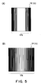
- Each pattern TPX constituting the test pattern TP has, as shown in FIG. 5A, an opening portion for producing a predetermined periodic component on a pupil plane 10 a of the projection optical system 10 , as well as periodic opening portions formed at the opposite sides of the aforementioned opening portion and for producing a periodic component different from the aforesaid periodic component, upon the pupil plane 10 a of the projection optical system 10 , such that substantially only zeroth order light passing through the pupil plane 10 a of the projection optical system 10 contributes to the imaging.
- FIG. 5A an opening portion for producing a predetermined periodic component on a pupil plane 10 a of the projection optical system 10 , as well as periodic opening portions formed at the opposite sides of the aforementioned opening portion and for producing a periodic component different from the aforesaid periodic component, upon the pupil plane 10 a of the projection optical system 10 , such that substantially only zeroth order light passing through the pupil plane 10 a of the projection optical system 10 contributes to the imaging.
- the projection optical system 10 comprises lines and spaces in which, with respect to a repetition direction thereof and from the center to the periphery, the lines or spaces have a substantially regular pitch while the widths of the spaces decrease gradually, such that substantially only zeroth order light passing through the pupil plane 10 a of the projection optical system 10 contributes to the imaging, and that adjacent lines are not resolvable by the projection optical system 10 .
- FIG. 2 a projection exposure apparatus having a measurement mode for measuring wavefront aberration of a projection optical system in accordance with the optical characteristic measuring method described above, will be explained as a second embodiment of the present invention.
- the projection optical system 10 not only a projection optical system (projection lens) using lenses but also a projection optical system using mirrors, or a projection optical system having a combination of lenses and mirrors, or the like, are applicable.
- FIG. 2 denoted at 1 is a high pressure Hg lamp which emits exposure light.
- the exposure light emitted from the light source 1 is collected by an elliptical mirror 1 a and, after this, it goes through an input lens 2 and is incident on a light entrance surface 3 a of a fly's eye lens 3 .
- a rear (test reticle 9 side) focal plane 3 b of the fly's eye lens 3 there are a large number of secondary light sources formed.
- Exposure light emitted from these secondary light sources goes by way of a variable aperture stop 4 , a first relay lens 5 , a projection type reticle blind 6 , a second relay lens 7 , and a main condenser lens 8 , and it illuminates the test reticle 9 with uniform illuminance.
- the rear focal plane 3 b of the fly's eye lens 3 is approximately conjugate with the pupil plane 10 b of the projection optical system 10 .
- the aperture diameter of the aperture stop 4 is variable.
- a measured value (aberration) obtained in accordance with a measuring method (to be described later) may be fed back to a control system of the exposure apparatus main assembly, such that various aberrations of the projection optical system 10 can be corrected by various methods and means known in the art.
- a correcting optical system 162 inside the projection optical system 10 may be driven by driving means 161 or, alternatively, through the control system and as shown in FIG. 17, the emission wavelength of a laser 172 (i.e. center wavelength of laser light) may be changed by wavelength changing means 171 .
- the projection exposure apparatus of FIG. 17 differs from the apparatus of FIG. 2 in the point of illumination system having a laser 172 as a light source and use of wavelength changing means 171 .
- the test reticle 9 is placed on a reticle stage 18 , and the position of the test reticle 9 can be changed by moving the reticle stage 18 along X-Y plane.
- a scope 19 is provided to observe a mark on the test reticle 9 and a reticle reference mark 21 provided inside the apparatus major assembly, simultaneously, thereby to measure deviation of the test reticle 9 with respect to the reticle reference mark 21 in X and Y directions.
- the reticle 9 can be brought into alignment with the apparatus major assembly (projection optical system 10 ).
- the scope 19 is provided with a driving system capable of moving it to any X and Y positions upon the test reticle 9 .
- test pattern 15 is constituted by plural patterns, and each pattern has a form such as shown in FIGS. 5A or 5 B.
- the projection type reticle blind 6 and the pattern bearing surface of the test reticle 9 are conjugate with each other, and an illumination region on the test reticle 9 is defined by means of the aperture of the projection type reticle blind 6 .
- a light blocking portion having a pinhole 16 .
- a region including the pinhole 16 is set as an illumination region on the test reticle 9 , and, by illuminating this region, light beams passed through the pinhole 16 of the light blocking portion illuminate plural patterns of the test pattern 15 formed on the lower surface of the test reticle 9 , from mutually different directions. These patterns of the test pattern 15 are projected upon a photosensitive substrate (wafer) W by the projection optical system 10 .
- FIG. 3 is an enlarged view of the detection system 11 of FIG. 2.
- a plate 11 a, a slit 11 b, and a light receptor 11 c constitute the detection system 11 .
- the plate 11 a is formed with the slit 11 b, and the light passed through the slit 11 b is received by the light receptor 11 c, whereby it is photoelectrically converted into an electric signal.
- the signal is transmitted to a processing unit, not shown, through a signal line, not shown. By this unit, the position of a pattern image as projected on the plate 11 a is detected.
- the wafer stage 12 comprises an X-Y stage 12 a capable of positioning the detection system 11 at arbitrary positions along a plane perpendicular to the optical axis 10 b of the projection optical system 10 , a Z stage 12 b capable of moving the detection system upwardly and downwardly in a direction parallel to the optical axis 10 b of the projection optical system 10 to thereby set the focus position of the detection system 11 , and so on.
- an autofocus system 13 for detecting the position of the detection system 11 in the optical axis 10 b direction.
- the autofocus system 13 comprises a light sending system 13 a for projecting a detecting slit-like light pattern (image), for example, onto the plate 11 a of the detection system 11 from a direction being oblique with respect to the optical axis 10 b of the projection optical system 10 , and a light receiving system 13 b for re-imaging the image of this slit-like pattern upon a photoelectric detector 13 c by use of reflection light from the plate 11 a.
- a light sending system 13 a for projecting a detecting slit-like light pattern (image), for example, onto the plate 11 a of the detection system 11 from a direction being oblique with respect to the optical axis 10 b of the projection optical system 10
- a light receiving system 13 b for re-imaging the image of this slit-like pattern upon a photoelectric detector 13 c by use of reflection light
- the position of the surface of the plate 11 b in the optical axis 10 b direction can be held at a predetermined position (image plane position of the projection optical system 10 ).
- the focus signal changes approximately rectilinearly with a change in height of the plate 11 a within a predetermined range (predetermined range in the optical axis 10 b direction)
- a change in focus position can be detected from a change in level of the focus signal.
- the Z stage 12 b of the wafer stage 12 has a level sensor (not shown) incorporated therein, for detecting the position of the Z stage itself in the optical axis 10 b direction of the projection optical system 10 .
- the wafer alignment system 14 detects alignment marks formed adjacent each shot areas on the wafer W, respectively. In this case, by detecting the spacing between the optical axis 10 b and an optical axis 14 a of the wafer alignment system 14 , that is, what is called a baseline quantity BD, in advance, alignment of each shot area of the wafer 11 can be accomplished accurately on the basis of the alignment mark position as measured by the wafer alignment system 14 . Further, the wafer alignment system 14 can be used to detect various marks.
- the illumination system of the exposure apparatus of this embodiment it is necessary but sufficient that, as a result of illumination, there is produced one or more aerial images or transferred pattern images whose positions on the image plane of the optical system 10 should be measured, and that the test reticle is illuminated with illumination light having a principal ray LP advancing along a direction (predetermined tilt angle and also predetermined azimuth angle) which is determined in dependence upon the positional relationship of the illumination light, in a direction along the plane of incidence upon the reticle 9 , between the center of the pinhole PH above the pattern that corresponds to the position of each aerial image or transferred pattern image TPa and the center of that pattern.
- both of the test pattern 15 and the light blocking portion having the pinhole 16 may not be formed on a reticle.
- the light blocking portion may be formed on a separate plate for pinhole.
- the pinhole 16 has a scattering element provided therein, such that light from an effective light source is scattered by this element, whereby light beams of ⁇ >1 are emitted from the pinhole 16 .
- the aperture shape of the variable stop 4 may have a ring-like (annular) shape and, in that occasion, an effective light source in which brightness is higher at the periphery than at the center thereof can be produced.
- FIG. 7 shows details of the test pattern 15 to be formed on the test reticle 9 .
- FIG. 7 denoted at 20 a is a mark which constitutes the test pattern 15 . Some portions of the grid-like mark 20 a are provided by the above-described patterns TPX shown in FIGS. 5A or 5 B.
- the longitudinal and lateral lines constituting the mark 20 a are designed with the same linewidth. Where these lines are the same as the pattern shown in FIG. 5, the linewidth is 2 microns, for example.
- a scattering element is provided inside the pinhole 16 formed on the rear face (upper surface) of the glass substrate 9 G of the reticle 9 , to cause the light for illuminating the reticle 9 to be scattered and diffused.
- a convex lens 17 may be disposed on the pinhole 16 as shown in FIG. 10, or a grating pattern having a diffusing effect may be provided inside the pinhole 16 , by which illumination condition of ⁇ 1.0 is attainable. Also in the case having such structure, use of a circular effective light source or a ring-like effective light source having a large a (coherence factor) is effective.
- the above-described test pattern 15 is illuminated under the illumination condition ⁇ 1.0, and images of the plural patterns TPX of the test pattern 15 by the projection optical system 10 are imaged upon the plate 11 a of the detection system 11 mounted on the wafer stage 12 .
- the intensity or quantity of light passing through the slit 11 b of the plate 11 a as the wafer stage 12 is moved and scanned in a horizontal direction (X or Y direction), is detected by the photoelectric detector 11 c.
- a detection signal such as shown in FIG. 4 corresponding to the light intensity or light quantity as detected at each X or Y position of the stage 12 (slit 11 b ), is obtainable.
- the center position of a single line of the mark 20 a of the test pattern 15 i.e. pattern TPX or TPY, as imaged on the plate 11 a, can be detected.
- central position information of the pattern images each representing the state of the wavefront at a corresponding position on the pupil plane of the projection optical system 10 is obtainable.
- the wavefront aberration of the optical system 10 is detected.
- the length and width of the slit 11 b of the detection system 11 are set to be not greater than the grid pitch of the aerial image of the grid-like mark 20 a and also to prevent an aerial image of a pattern TPX, next to an aerial image of a pattern TPX of a single line which is just the subject of measurement, from coming into the slit 11 b.
- this embodiment has an arrangement that, in relation to an image of a pattern TPX of longitudinal lines and an image of a pattern TPY of lateral lines, separate pairs of slits 11 b and photoelectric detectors 11 c are prepared.
- the projection exposure apparatus into which a test reticle of the third embodiment is introduced is a projection exposure apparatus such as shown in FIGS. 1, 2 or 17 .
- the test reticle 9 is provided by two plates, that is, a pinhole plate 9 a having a light blocking portion with a pinhole 16 formed on the upper surface (or lower surface) thereof and a pattern plate 9 b having a test pattern 15 formed on the upper surface (or lower surface) thereof.
- test pattern 15 the pinhole 16 and the diffusing means 18 such as a scattering element or the like are similar to those in the first and second embodiments.
- diffusing means 18 such as a scattering element or the like.
- the optical characteristic measurement unit comprises two plates
- a pinhole plate 9 a has a convex lens (positive lens) 17 as diffusing means disposed on a pinhole 16
- a pattern plate 9 b has a mark 20 a of the test pattern 15 formed on the upper surface (or lower surface) thereof.
- the convex lens 17 and the light blocking portion with the pinhole 16 may be formed either the upper surface or the lower surface of the pinhole plate 9 a.
- a dust protection glass (not shown) is provided above the reticle for prevention of contamination thereof.
- the dust protection glass may conveniently be made detachably mountable so that the dust protection glass and the upper (light source side) plate of the two plates, for example, the plate 9 a of FIGS. 11, 12 and 20 - 22 , are made mutually interchangeably.
- a large distinction of the measurement sequence of this embodiment over the measurement sequence of the first and second embodiments resides in that an alignment operation for registering the center of a pinhole 16 with the center of a test pattern 15 , is incorporated.
- a test reticle 9 (plate 9 b in which a test pattern 15 is formed on the substrate front face (lower surface) but a light blocking portion with a pinhole is not formed on the substrate rear face (upper surface) which is inside an exposure apparatus is loaded on a reticle stage 18 .
- a pinhole plate 9 a inside the exposure apparatus is loaded to between the test reticle 9 and a scope 19 .
- the center of the pinhole 18 or 16 on the pinhole plate 9 a can be set at a predetermined X-Y position, with an error within the mechanical precision.
- an alignment mark of the test reticle 9 and a reticle reference mark 21 are observed through the scope 19 to detect a relative positional deviation between the reticle and the apparatus major assembly, and relative alignment of them is carried out by moving the reticle 9 in X and Y directions by use of the reticle stage 20 to adjust the position thereof.
- the scope 19 is moved to an observation position (illumination position) for measurement of wavefront aberration and, simultaneously, the detection system 11 on the wafer stage 12 is moved to a predetermined (X, Y and Z) coordinate position which is an observation position (detection position) for the wavefront aberration measurement.
- the detection system 11 determines whether the central position of an image of a predetermined pattern, of the test pattern 15 , with respect to a reference position. Further, the detection system 11 is moved in Z direction (optical axis 10 b direction) by a predetermined amount, and again the amount of positional deviation of the central position of the image of the same predetermined pattern from the reference position, at a Z (direction) position different from that in the preceding measurement, is carried out. This is repeated several times.
- the pattern to be measured is the entire pattern (all lines of the grid-like mark) which constitutes the test pattern 15 .
- the position (deviation) of the central position of each of the images of the patterns of the two, longitudinal and lateral lines, is measured.
- positional deviations dx and dy of the center of the test pattern 15 of the pattern plate 9 b and of the center of the pinhole 16 of the pinhole plate 9 a are proportional to the positional deviation amounts dsx/dZ and dsy/dZ of the pattern images of the above-described two, longitudinal and lateral lines, and therefore, they can expressed by the following equations.
- the positional deviation amount of the pinhole 16 and the test pattern 15 can be calculated.
- the test pattern 15 of the reticle 9 is moved and positional alignment between the test pattern 15 center and the pinhole 16 center along the X-Y plane is carried out.
- a closed loop is also possible, such that the scope 19 may be moved to the reticle reference mark position to observe the alignment mark of the test reticle 9 and the reticle reference mark 21 thereby to measure the movement amount of the reticle stage 20 , and any remainder may be again fed back to a driving system for the reticle stage 20 .
- This alignment process is repeated until the positional deviations dx and dy come into a tolerable range and, after that, measurement of wavefront aberration of the projection optical system 10 is performed in accordance with the same sequence as of the flow of FIG. 15.
- the scope 19 is retracted so as not to interfere with the illumination light.
- test reticle to be used for measurement of wavefront aberration of the projection optical system 10
- the aerial image of each pattern of this test reticle is large in size such as few microns
- a CCD or a linear sensor may be directly placed on the pattern imaging plane, without incorporating an enlarging optical system, to detect light intensity distribution or light quantity distribution of the aerial image.
- X-Y motion of the wafer stage 12 is unnecessary, for detection of the light intensity distribution or light quantity distribution of the aerial image (pattern image).
- the pattern images may be transferred onto a substrate mounted on the wafer stage 12 and having a photochromic material layer formed thereon, and the central positions of the thus transferred pattern images may be measured by using the off-axis alignment detection system 14 .
- the off-axis alignment detection system 14 In this occasion, as compared with a case in which pattern images are transferred to a certain type resist, a developing process is unnecessary.
- FIG. 17 shows an example in which, in the first embodiment, a laser 172 is used as a light source. Basic structure thereof is the same as of FIG. 1.
- the optical characteristic measuring method of the present invention can be applied as a calibration technique for a separate measuring system such as an optical characteristic measuring system using an interferometer.
- a separate measuring system such as an optical characteristic measuring system using an interferometer.
- the wavefront aberration amount of a projection lens mounted inside a projection exposure apparatus has to be substituted by a wavefront aberration amount of a projection lens as measured, with respect to the projection lens alone, by using an interferometer system inside an exposure apparatus manufacturing factory.
- the present method which is small in load to exposure apparatus or small in system load is used, and measurement of wavefront aberration of a projection lens is carried out both upon the exposure apparatus major assembly and upon the interferometer system. Based on this, the measurement result (wavefront aberration amount) obtained by use of the interferometer system inside the exposure apparatus manufacturing factory is calibrated.
- an optical characteristic measuring method including a sequence in which images of patterns of a test pattern 15 are transferred to a photosensitive substrate (wafer) W and the transferred images are developed, and in which central positions of the transferred images, thus developed, are measured.
- the test pattern to be used is two types of patterns shown in FIGS. 7 and 8, and they are formed on a common test reticle 9 .
- the exposure apparatus in which the optical characteristic of a projection optical system is to be measured by use of the reticle 9 is a projection exposure apparatus such as shown in FIGS. 1, 2 or 17 .
- the test pattern shown in FIG. 7 is constituted by a pattern group 20 a, defining a grid-like mark.
- Patterns TPX and TPY of the pattern group may have a shape such as shown in FIGS. 5A or 5 B, but the fourth embodiment uses a mark of a type defining a pattern of linewidth of 2-3 microns upon a wafer, and having a shape shown in FIG. 5B.
- a light blocking portion with a pinhole whose central position is coincident with the center of the mark 20 a.
- This reticle has a basic structure such as shown in FIGS. 9 or 10 , like the first and second embodiments. However, as compared with the first and second embodiments, it is provided with a grid-like mark 21 a shown in FIG. 8, as a new pattern.
- the grid-like mark 21 a is a reference pattern group for measuring relative positional deviations of the patterns of the test pattern 15 .
- light beams from an illumination system are projected uniformly on the reference patterns of the grid mark 21 a, such that these reference patterns are illuminated with light beams of substantially the same intensity and from the same direction, and they are imaged upon the photosensitive substrate through the projection optical system 10 .
- FIGS. 13 and 14 are fragmentary sectional views, respectively, showing examples of the test reticle in the fourth embodiment.
- FIG. 13 shows an example in which a light blocking portion having a pinhole 16 is formed on a rear face (upper surface) of the substrate of the test reticle 9 , while a pattern group 20 a and a reference pattern group 18 as a test pattern are formed on the front face (lower surface) of the substrate.
- FIG. 14 shows a case using two plates, that is, a pattern plate 9 b having a pattern group 20 a and a reference pattern group 18 as a test pattern formed on the front face (lower surface) of a substrate, and a pinhole plate 9 a having a light blocking portion with a pinhole 16 formed on the rear face (upper surface) of a separate substrate.
- Each of the reticles shown in FIGS. 13 and 14 has a scattering element or a grating pattern provided inside the pinhole 16 . Due to the function of this element inside the pinhole, the pattern group 20 a is illuminated with a condition ⁇ >1.
- test reticle 9 is illuminated under a standard illumination condition (1.0> ⁇ >0.7) and the marks 20 a and 21 a of the test pattern are illuminated, and images of these patterns are projected and transferred to a photosensitive substrate through the projection optical system 10 .
- the wafer stage 12 or alternatively the reticle stage 20 is moved so that the marks 20 a and 21 a are positionally superposed one upon another.
- the marks 20 a and 21 a are illuminated with the standard illumination condition and, under the influence of a scattering element, a grating pattern or a convex lens, the test pattern is illuminated with an illumination condition ⁇ >1.0, light beams being projected to the patterns of the pattern group 20 a from mutually different directions.
- the images of these patterns are projected and transferred to the photosensitive substrate through the projection optical system 10 .
- images of the pattern groups of the marks 20 a and 21 a are transferred to the photosensitive substrate.
- a relative positional deviation between corresponding pattern images is measured by use of a measuring tool known in the art.
- calculation is carried out to detect the wavefront of the projection optical system 10 at the pupil plane 10 a, and the wavefront aberration of the projection optical system 10 as well as various aberrations (Seidel's five aberrations) are detected.
- the state of aberrations as measured may be fed back to the major assembly, to perform aberration correction of the projection lens.
- test patterns 15 and pinholes 16 may be provided at several locations, on one and the same reticle 9 , having different image heights. This enables wavefront aberration measurements with respect to different image heights.
- FIG. 18 shows the sequence of measurement using the test reticle of FIG. 13, and FIG. 19 shows the sequence of measurement using the test reticle of FIG. 14.
- the exposure sequence using the pinhole plate 9 a also it is carried out in accordance with the sequence such as shown in FIG. 19.
- FIG. 20 shows another example of the test reticle, as a fifth embodiment of the present invention.
- the exposure apparatus in which the optical characteristic of a projection optical system is to be measured by use of the test reticle is a projection exposure apparatus such as shown in FIGS. 1, 2 or 17 .
- the test reticle shown in FIG. 20 is an example in which a light blocking portion with a pinhole 16 and a pattern group 20 a of a test pattern are formed on the upper surface (rear face) and the lower surface (front face) of a common plate (glass) 9 b, respectively, and in which a plate (glass) 9 a having a scattering element 22 for light diffusion for accomplishing illumination of the pattern group 20 a under an illumination condition ⁇ >1.0, being formed on the lower surface, is disposed above the pattern plate 9 b.
- the scattering element for diffusion a ground glass for scattering light or a diffraction grating such as CGH or the like for scattering light, may be used.
- an effective light source having a brightness higher at the periphery than at the center is produced by the illumination system.
- the size and shape thereof By optimizing the size and shape thereof, non-uniformness of illuminance upon the pinhole 16 or test pattern 20 a can be removed, and the illuminance distribution can be made uniform.
- the illuminance uniformness refers to a state in which the intensities of plural light beams projected to the patterns of the pattern group 20 a from mutually different directions are made substantially uniform. If such state is accomplished, the exposure amounts for exposure of plural pattern images become substantially constant, and thus the produced pattern images have the same linewidth. This reduces an error based on the exposure amount, in the aberration measurement or positional deviation detection for pattern image.
- the position of the plate 9 a having a scattering element 22 it may be placed anywhere if it is on the effective light source side of (i.e. above) the test reticle 9 .
- it can be placed adjacent the projection type reticle blind 6 of FIGS. 2 or 17 or at a desired position inside the illumination system.
- the plate 9 a can be mounted in place of a dust protection glass just above the reticle stage and disposed at this position.
- a member for holding the dust protection glass and the plate 9 a it may either be fixed to the illumination system or be held by the major assembly (projection optical system).
- FIG. 21 shows another example of the test reticle, as a sixth embodiment of the present invention.
- the exposure apparatus in which the optical characteristic of a projection optical system is to be measured by use of the test reticle is a projection exposure apparatus such as shown in FIGS. 1, 2 or 17 .
- FIG. 21 is a modified form of the examples of FIGS. 11 and 20.
- a pattern group 20 a of the test pattern is formed on the front face (lower surface) of the pattern plate b.
- a light blocking portion with a pinhole 16 as well as a scattering element 22 for light diffusion are formed on a separate pinhole plate 9 a.
- the plate 9 a is disposed above the reticle 9 b.
- relative alignment of the center of the pinhole 16 and the center of the pattern group 20 a can be accomplished by moving the reticle stage 20 . Further, the reticle 9 b and the plate 9 a may have alignment marks 23 , and these marks may be observed through the scope 19 . With this procedure, relative positional deviation between these plates can be measured directly.
- any deviation between the center of the pinhole 16 and the center of the test pattern 20 a along a horizontal direction causes a deviation of imaging light ray from the pupil center of the projection lens 10 .
- the reference coordinate (pupil center reference) for the wavefront calculation differs from the actually measured coordinate of the measurement point.
- This is one error factor for wavefront aberration measurement.
- the pinhole 16 and the test pattern 20 a are formed on different plates, respectively, and the relative alignment of them is carried out by the reticle stage. With this arrangement, the measurement precision can be increased.
- light blocking portions with pinholes 16 and pattern groups 20 a of the test pattern may be formed on a glass substrate in such manner that: plural sets of pinholes and test patterns 20 a are disposed in juxtaposition with each other, while each set is designed so that the center of the pinhole and the center of the test pattern have a small amount of mutual deviation.
- the light blocking portions with pinholes 16 and the pattern groups 20 a of the test pattern are formed on a glass substrate.
- an optical characteristic measuring method and a reticle usable therefor which can be suitably used for high-precision measurement of an optical characteristic such as wavefront aberration, for example, are accomplished.
Abstract
In an optical characteristic measuring method for measuring an optical characteristic of a projection optical system (10 a), a reticle (9) having a plurality of patterns (TP) is supplied, and scattered light from an aperture is directed to said plurality of patterns (TP), whereby light beams are projected onto said plurality of patterns in mutually different directions, by which images of said plurality of patterns are formed through said projection optical system (10 a) Positions of images of said plurality of patterns, respectively, are detected and, by use of the result of detection, the optical characteristic of said projection optical system is detected. This accomplishes an optical characteristic measuring method and a reticle to be used therefor, which are suitable for measuring an optical characteristic of an optical system such as wavefront aberration, for example, at high precision.
Description
- This invention relates to a method of measuring an optical characteristic of a projection optical system and a reticle to be used in that method. For example, the invention is suitable for measurement of an optical characteristic, such as wavefront aberration, for example, of a projection optical system of a projection exposure apparatus which is used in a lithographic process for manufacture of semiconductor devices, liquid crystal display devices, thin film magnetic heads, or the like.
- The manufacture of semiconductor devices, liquid crystal display devices, thin film magnetic heads, or the like, based on a lithographic process uses a projection exposure apparatus for projecting an image of a pattern of a photomask or reticle (hereinafter, simply “reticle”) onto a photosensitive substrate through a projection optical system (e.g. projection lens). In such projection exposure apparatus, a decrease of pattern resolving power resulting from aberrations of the projection optical system remaining due to the design thereof or manufacture of thereof becomes a large problem.
- In consideration of this, technology for very precisely measuring the optical characteristic of a projection optical system such as aberration has been desired.
- Aberrations of a projection lens such as spherical aberration, image plane (curvature of field), astigmatism (astigmatic aberration), coma (coma aberration), wavefront aberration, and etc. are measured, and it is used for practical evaluation and inspection. Among these aberrations, the wavefront aberration is very the aberration. By approximating this wavefront aberration on the basis of generally used Zernike polynomial or the like, aberrations such as coma, astigmatism, image plane, spherical aberration which are factors of the polynomial can also be calculated. Also from the standpoint of prediction of process margin for a wide variety of device patterns based on simulations, the measurement of wavefront aberration is regarded as important.
- Wavefront aberration measuring methods are proposed in U.S. Pat. Nos. 5,828,455 and 5,978,085, for example. In the measuring methods proposed there, a grid-like pattern is provided on a reticle pattern surface and a pinhole is provided right below the center of the grid-like pattern with a small spacing kept from it. Further, on the retile upper surface, there is a special reticle having a convex lens placed just above the center of the grid-like pattern. When this reticle is illuminated by an illumination system of an exposure apparatus, due to the aforementioned convex lens the illumination angle (NA) of the illumination light emitted from the illumination system is made into an angle not less than σ1, and this light illuminates the grid pattern below it. Light passed through the grid pattern goes through the pinhole below it. At this time, the light that can pass through the pinhole is limited only to such light having an angle connecting the position of each point on the grid pattern and the aforementioned pinhole. Therefore, lights emitted from respective points on the grid pattern advance in the form of plural lights having mutually different angles.
- These lights having mutually different angles arrive at mutually different positions upon a pupil plane of the projection lens and, while being influenced by the wavefront aberration of the projection lens, they reach a wafer surface to image each points of the grid pattern thereon. Here, the images of each points of the imaged grid pattern have been influenced by the wavefront aberration (phase) differently. Namely, since a light ray advances in a direction of a normal to the wavefront, the imaging position of an image of each point on the grid pattern shifts from an idealistic position by an amount corresponding to the tilt at a corresponding point on the wavefront. In consideration of this, by measuring the deviations, from an idealistic grid, of images of each points of the grid pattern, tilts of the wavefront at each points on the pupil plane are obtained and, by using various mathematical techniques, the wavefront is calculated.
- The wavefront measuring methods proposed in aforementioned U.S. Pat. Nos. 5,828,455 and 5,978,085 are a method close to well-known Hartman's method. In Hartman's method, a pinhole is disposed on a pupil plane of a projection lens to restrict the position of the wavefront and, from a positional deviation of a pattern image which is formed by light passed therethrough and imaged, the tilt of the wavefront is detected.
- In Hartman's method, by placing a pinhole on the pupil plane, the object spectrum bears, according to equation (1) below and by the pinhole filter, only information of a certain small wavefront region.
- E(x)=F-1[G(f)·p(f)·w(f)] (1)
- F-1: Fourier inverse transform
- E(x): optical amplitude function of image
- G(f): object spectrum
- w(f) :pupil (wavefront) function
- p(f): pinhole function
- Although it is desirable to control the shape of the object spectrum (pupil filtering) surely by placing a pinhole on a pupil plane as in Hartman's method, in practical exposure apparatuses, it is difficult because of the space of a barrel, a purge structure for contamination prevention, or the like, and also in respect to the cost.
- In the methods proposed in aforementioned U.S. Pat. Nos. 5,828,455 and 5,978,085, the pinhole filter is placed just below the reticle. Therefore, the object spectrum on the pupil plane is, unlike the equation (1) above, Fourier transform including a phase term.
- An object of the present invention is to provide an optical characteristic measuring method suitable for high-precision measurement of an optical characteristic of an optical system such as wavefront aberration, for example, and a reticle to be used in such measuring method.
- Another object of the present invention is to provide an optical characteristic measuring method which enables measurement of an optical characteristic such as wavefront aberration, for example, in a completely different way from the methods disclosed by the aforementioned two U.S. patents, and a reticle to be used in such measuring method.
- A further object of the present invention is to provide a projection exposure apparatus into which an optical characteristic measuring method or a reticle, described above, can be incorporated.
- A first aspect of the present invention concerns an optical characteristic measuring method for measuring an optical characteristic of a projection optical system, characterized in that:
- a reticle having a plurality of patterns is supplied;
- scattered light from an aperture is directed to said plurality of patterns, whereby light beams are projected on said plurality of patterns in mutually different directions, by which images of said plurality of patterns are formed through said projection optical system; and
- positions of the images of said plurality of patterns are detected and, by use of the result of detection, the optical characteristic of said projection optical system is detected.
- A second aspect of the present invention concerns the first aspect, and it is characterized in that a light blocking member having said aperture is present on said reticle.
- A third aspect of the present invention concerns the first aspect, and it is characterized in that a light blocking member having said aperture is present above said reticle.
- A fourth aspect of the present invention concerns the second or third aspect, and it is characterized in that there is a scattering portion for producing the scattered light.
- A fifth aspect of the present invention concerns the fourth aspect, and it is characterized in that said scattering portion is present inside said aperture.
- A sixth aspect of the present invention concerns the fourth aspect, and it is characterized in that said scattering portion is present between a light source and said aperture.
- A seventh aspect of the present invention concerns the first to sixth aspects recited in claims 1-6, and it is characterized in that said scattering portion is illuminated by use of an effective light source in which, as like a ring, for example, a central portion is darker than a peripheral portion.
- An eighth aspect of the present invention concerns the first to seventh aspects recited in claims 1-7, and it is characterized in that said aperture is a pinhole.
- A ninth aspect of the present invention concerns the first to eighth aspects, and it is characterized in that said pattern has an opening portion for producing a predetermined periodic component on a pupil plane of said projection optical system as well as periodic opening portions defined at opposite sides of that opening portion and for producing a periodic component, different from said periodic component, on the pupil plane of said projection optical system.
- A tenth aspect of the present invention concerns the first to eighth aspects, and it is characterized in that said pattern has lines and spaces in which, with respect to a direction of repetition and from a center to a periphery, said spaces have a substantially regular pitch while widths of said spaces gradually decrease, and in which adjacent lines are not resolvable by said projection optical system.
- An eleventh aspect of the present invention concerns the first to eighth aspects, and it is characterized in that said pattern has lines and spaces for directing substantially only zeroth order light to an image plane of said projection optical system.
- A twelfth aspect of the present invention concerns the first to eleventh aspects, and it is characterized in that said detecting step includes a step of photoelectrically converting an aerial image of said lines and spaces.
- A thirteenth aspect of the present invention concerns the first to eleventh aspects, and it is characterized in that said detecting step includes a step of exposing a photosensitive substrate with an image of said lines and spaces, and a step of developing the photosensitive substrate.
- A fourteenth aspect of the present invention concerns the first to fourteenth aspects, and it is characterized in that said optical characteristic includes wavefront aberration.
- A fifteenth aspect of the present invention concerns a projection exposure apparatus characterized by having a mode for measuring an optical characteristic of a projection optical system in accordance with a measuring method of any one of the first to fourteenth aspects, and by having an illumination system for projecting illumination light to said test pattern when said reticle is supplied to the apparatus.
- A-sixteenth aspect of the present invention concerns a device manufacturing method characterized by supplying a reticle for device manufacture to a projection exposure apparatus according to the fifteenth aspect, and by exposing a substrate with a pattern of the reticle.
- A seventeenth aspect of the present invention concerns a reticle, characterized by: a plurality of patterns formed on a front face of a substrate; and a light blocking portion with an aperture, being formed on a rear face of said substrate, and a light scattering portion for producing scattered light from said aperture.
- An eighteenth aspect of the present invention concerns the seventeenth aspect, and it is characterized in that said aperture is a pinhole.
- A nineteenth aspect of the present invention concerns the seventeenth aspect, and it is characterized in that said light scattering portion is present inside said aperture.
- A twentieth aspect of the present invention concerns a measurement unit for measuring an optical characteristic of a projection optical system, characterized by a reticle having a plurality of patterns formed on a front face of a substrate, and a light blocking portion with an aperture, being formed on a rear face of said substrate, as well as a light scattering portion for producing scattered light from said aperture.
- A twenty-first aspect of the present invention concerns the seventeenth aspect, and it is characterized in that said aperture is a pinhole.
- A twenty-second aspect of the present invention concerns the twentieth aspect, and it is characterized in that said light blocking portion is formed on a rear face of said substrate, and said light scattering portion is formed on another substrate.
- A twenty-third aspect of the present invention concerns the twenty-first aspect, and it is characterized in that said light scattering portion is formed on a reticle side surface of said other substrate.
- A twenty-fourth aspect of the present invention concerns the twentieth aspect, and it is characterized in that said light blocking portion and said light scattering portion are formed on another substrate.
- A twenty-fifth aspect of the present invention concerns the twenty-third aspect, and it is characterized in that said light blocking portion is formed on a reticle side surface of said other substrate, and said light scattering portion is formed on a surface of said other substrate, opposite to the reticle side.
- A twenty-sixth aspect of the present invention concerns the twenty-third aspect, and it is characterized in that said light blocking portion and said light scattering portion are formed on a surface of said other substrate, opposite to the reticle side.
- FIG. 1 is a schematic view of a main portion of a projection exposure apparatus according to a first embodiment of the present invention.
- FIG. 2 is a schematic view of a projection exposure apparatus according to a second embodiment of the present invention.
- FIG. 3 is a view for explaining a
detection system 11 in FIG. 2. - FIG. 4 is a view for explaining light intensity distribution of a pattern image.
- FIG. 5 is a view for explaining a pattern structure of a test pattern according to the present invention.
- FIG. 6 is a view for explaining specific disposition of a test pattern according to the present invention.
- FIG. 7 is a view for explaining a
mark 20 a in FIG. 6. - FIG. 8 is a view for explaining a
mark 21 a in FIG. 6. - FIG. 9 is a sectional view of an example of a test reticle according to the present invention.
- FIG. 10 is a sectional view for explaining another example of a test reticle according to the present invention.
- FIG. 11 is a sectional view for explaining a pattern plate and a pinhole plate, in a further example of a test reticle according to the present invention.
- FIG. 12 is a sectional view for explaining a pattern plate and a pinhole plate, of a test reticle according to the present invention.
- FIG. 13 is a sectional view for explaining a yet further example of a test reticle according to the present invention.
- FIG. 14 is a sectional view for explaining a pattern plate and a pinhole plate, in a still further example of a test reticle according to the present invention.
- FIG. 15 is a flow chart of aberration measurement according to the present invention.
- FIG. 16 is a flow chart of aberration measurement according to the present invention.
- FIG. 17 is a schematic view of another example of exposure apparatus according to the present invention.
- FIG. 18 is a flow chart of aberration measurement according to the present invention.
- FIG. 19 is a flow chart of aberration measurement according to the present invention.
- FIG. 20 is a sectional view for explaining a pattern plate and a pinhole plate, in a still further example of a test reticle according to the present invention.
- FIG. 21 is a sectional view for explaining a pattern plate and a pinhole plate, in a still further example of a test reticle according to the present invention.
- FIG. 22 is a sectional view for explaining a pattern plate and a pinhole plate, in a still further example of a test reticle according to the present invention.
- Figure is a schematic view of a main portion of an exposure apparatus according to a first embodiment of the present invention.
- The first embodiment shows a projection exposure apparatus for projecting a circuit pattern onto a photosensitive substrate through a projection optical system. The exposure apparatus of the first embodiment has a measurement mode for measuring wavefront aberration of an optical system (projection lens) in accordance with an optical characteristic measuring method of the present invention. As a matter of course, similar measurement may be made to this optical system during the manufacture of the exposure apparatus.
- In FIG. 1, denoted at 9 is a test reticle. The
test reticle 9 has a pattern group (test pattern) TP formed on the lower surface (front face) of a substrate glass, as well as a light blocking portion with an aperture (pinhole) PH formed on the upper surface (rear face) of this glass. Measurement of wavefront aberration of the projection lens is performed as follows. - Illumination light from an effective
light source 4 of an illumination optical system, having a spread of an angle equivalent to σ>1 or σ=1, is projected to the pinhole PH at the upper surface of thetest reticle 9. With light beams passed through the pinhole PH (aperture) on the upper surface of thereticle 9, patterns of the test pattern TP formed on the lower surface of thereticle 9 are illuminated from mutually different directions. In response, the patterns of the test pattern TP are imaged by theprojection lens 10. The positions (deviations from a reference position) of aerial images of them or of transferred pattern images TPa of them being transferred to a photosensitive substrate W, are measured by means of a measuring tool of known type. Then, on the basis of positional information of these images, tilts of the wavefront at positions corresponding to each images, along thepupil plane 10 a, are calculated. From the results, the wavefront aberration of theprojection lens 10 is measured. Once the wavefront aberration is obtained, spherical aberration, coma aberration, curvature of field, astigmatic aberration and distortion aberration can be detected. - The test pattern TP and the light blocking portion having the pinhole PH may not be formed on one and the same plate as shown in FIG. 1. They may be formed on different plates. In summary, it is necessary but sufficient that there is one or more aerial images or transferred pattern images TPa whose positions should be measured, and that it is illuminated with illumination light having a principal ray LP advancing along a direction (predetermined tilt angle and also predetermined azimuth angle) which is determined in dependence upon the positional relationship of the illumination light, in a direction along the plane of incidence upon the
reticle 9, between the center of the pinhole PH above the pattern that corresponds to the position of each aerial image or transferred pattern image TPa and the center of that pattern. - Each pattern TPX constituting the test pattern TP has, as shown in FIG. 5A, an opening portion for producing a predetermined periodic component on a
pupil plane 10 a of the projectionoptical system 10, as well as periodic opening portions formed at the opposite sides of the aforementioned opening portion and for producing a periodic component different from the aforesaid periodic component, upon thepupil plane 10 a of the projectionoptical system 10, such that substantially only zeroth order light passing through thepupil plane 10 a of the projectionoptical system 10 contributes to the imaging. Alternatively, as shown in FIG. 5B, it comprises lines and spaces in which, with respect to a repetition direction thereof and from the center to the periphery, the lines or spaces have a substantially regular pitch while the widths of the spaces decrease gradually, such that substantially only zeroth order light passing through thepupil plane 10 a of the projectionoptical system 10 contributes to the imaging, and that adjacent lines are not resolvable by the projectionoptical system 10. - Next, referring to FIG. 2, a projection exposure apparatus having a measurement mode for measuring wavefront aberration of a projection optical system in accordance with the optical characteristic measuring method described above, will be explained as a second embodiment of the present invention.
- In the second embodiment, as regards the projection
optical system 10, not only a projection optical system (projection lens) using lenses but also a projection optical system using mirrors, or a projection optical system having a combination of lenses and mirrors, or the like, are applicable. - In FIG. 2, denoted at 1 is a high pressure Hg lamp which emits exposure light. The exposure light emitted from the
light source 1 is collected by anelliptical mirror 1 a and, after this, it goes through aninput lens 2 and is incident on alight entrance surface 3 a of a fly'seye lens 3. At a rear (test reticle 9 side)focal plane 3 b of the fly'seye lens 3, there are a large number of secondary light sources formed. Exposure light emitted from these secondary light sources goes by way of avariable aperture stop 4, afirst relay lens 5, a projectiontype reticle blind 6, asecond relay lens 7, and amain condenser lens 8, and it illuminates thetest reticle 9 with uniform illuminance. The rearfocal plane 3 b of the fly'seye lens 3 is approximately conjugate with the pupil plane 10 b of the projectionoptical system 10. Also, the aperture diameter of theaperture stop 4 is variable. - A measured value (aberration) obtained in accordance with a measuring method (to be described later) may be fed back to a control system of the exposure apparatus main assembly, such that various aberrations of the projection
optical system 10 can be corrected by various methods and means known in the art. For example, through the control system described above and as shown in FIG. 2, a correctingoptical system 162 inside the projectionoptical system 10 may be driven by drivingmeans 161 or, alternatively, through the control system and as shown in FIG. 17, the emission wavelength of a laser 172 (i.e. center wavelength of laser light) may be changed bywavelength changing means 171. This enables automatic correction or automatic setting of the aberration of the projectionoptical system 10. Here, the projection exposure apparatus of FIG. 17 differs from the apparatus of FIG. 2 in the point of illumination system having alaser 172 as a light source and use ofwavelength changing means 171. - Now, the
test reticle 9 is placed on areticle stage 18, and the position of thetest reticle 9 can be changed by moving thereticle stage 18 along X-Y plane. Ascope 19 is provided to observe a mark on thetest reticle 9 and areticle reference mark 21 provided inside the apparatus major assembly, simultaneously, thereby to measure deviation of thetest reticle 9 with respect to thereticle reference mark 21 in X and Y directions. By moving thestage 18 on the basis of the measurement result, thereticle 9 can be brought into alignment with the apparatus major assembly (projection optical system 10). Further, thescope 19 is provided with a driving system capable of moving it to any X and Y positions upon thetest reticle 9. Therefore, if necessary, by using thescope 19, it is possible to illuminate the region of atest pattern 15 at an arbitrary position on thereticle 9, with exposure light. Thetest pattern 15 is constituted by plural patterns, and each pattern has a form such as shown in FIGS. 5A or 5B. - The projection
type reticle blind 6 and the pattern bearing surface of thetest reticle 9 are conjugate with each other, and an illumination region on thetest reticle 9 is defined by means of the aperture of the projectiontype reticle blind 6. - On the upper surface of the
test reticle 9, there is a light blocking portion having apinhole 16. By means of the aperture of the projectiontype reticle blind 6, a region including thepinhole 16 is set as an illumination region on thetest reticle 9, and, by illuminating this region, light beams passed through thepinhole 16 of the light blocking portion illuminate plural patterns of thetest pattern 15 formed on the lower surface of thetest reticle 9, from mutually different directions. These patterns of thetest pattern 15 are projected upon a photosensitive substrate (wafer) W by the projectionoptical system 10. - The positions of aerial images of these patterns being imaged on an imaging plane of the projection
optical system 10 or of pattern images (developed or latent images) transferred to the photosensitive substrate W, are measured by use of known measuring means. - In this embodiment, by use of a
detection system 11 provided on thewafer stage 12, the positions of the aerial images of the patterns of thetest pattern 15 are detected. Through the projectionoptical system 10, the image of thetest pattern 15 is imaged on aplate 11 a which constitutes thedetection system 11 mounted on thewafer stage 12. FIG. 3 is an enlarged view of thedetection system 11 of FIG. 2. - In FIG. 3, a
plate 11 a, aslit 11 b, and alight receptor 11 c constitute thedetection system 11. Theplate 11 a is formed with theslit 11 b, and the light passed through theslit 11 b is received by thelight receptor 11 c, whereby it is photoelectrically converted into an electric signal. The signal is transmitted to a processing unit, not shown, through a signal line, not shown. By this unit, the position of a pattern image as projected on theplate 11 a is detected. - The
wafer stage 12 comprises an X-Y stage 12 a capable of positioning thedetection system 11 at arbitrary positions along a plane perpendicular to the optical axis 10 b of the projectionoptical system 10, aZ stage 12 b capable of moving the detection system upwardly and downwardly in a direction parallel to the optical axis 10 b of the projectionoptical system 10 to thereby set the focus position of thedetection system 11, and so on. - In this embodiment, there is an
autofocus system 13 for detecting the position of thedetection system 11 in the optical axis 10 b direction. Theautofocus system 13 comprises alight sending system 13 a for projecting a detecting slit-like light pattern (image), for example, onto theplate 11 a of thedetection system 11 from a direction being oblique with respect to the optical axis 10 b of the projectionoptical system 10, and alight receiving system 13 b for re-imaging the image of this slit-like pattern upon aphotoelectric detector 13 c by use of reflection light from theplate 11 a. - As the position of the
plate 11 a in the optical axis 10 b direction of the projectionoptical system 10 changes, in thelight receiving system 13 b there occurs a change in position, on thephotoelectric detector 13 c, of the re-imaged light pattern image. Thus, by detecting the position of this pattern image, the position of theplate 11 a in the optical axis direction can be detected. Thephotoelectric detector 13 c produces a signal (focus signal) which is variable with the position of the re-imaged pattern image. Thus, by moving theZ stage 12 b of thewafer stage 12 through acontrol system 13 d so that this signal is kept at a predetermined level, the position of the surface of theplate 11 b in the optical axis 10 b direction can be held at a predetermined position (image plane position of the projection optical system 10). - Also, since the focus signal changes approximately rectilinearly with a change in height of the
plate 11 a within a predetermined range (predetermined range in the optical axis 10 b direction), a change in focus position can be detected from a change in level of the focus signal. TheZ stage 12 b of thewafer stage 12 has a level sensor (not shown) incorporated therein, for detecting the position of the Z stage itself in the optical axis 10 b direction of the projectionoptical system 10. - Denoted at 14 is an off-axis type wafer alignment system. The
wafer alignment system 14 detects alignment marks formed adjacent each shot areas on the wafer W, respectively. In this case, by detecting the spacing between the optical axis 10 b and anoptical axis 14 a of thewafer alignment system 14, that is, what is called a baseline quantity BD, in advance, alignment of each shot area of thewafer 11 can be accomplished accurately on the basis of the alignment mark position as measured by thewafer alignment system 14. Further, thewafer alignment system 14 can be used to detect various marks. - For the illumination system of the exposure apparatus of this embodiment, it is necessary but sufficient that, as a result of illumination, there is produced one or more aerial images or transferred pattern images whose positions on the image plane of the
optical system 10 should be measured, and that the test reticle is illuminated with illumination light having a principal ray LP advancing along a direction (predetermined tilt angle and also predetermined azimuth angle) which is determined in dependence upon the positional relationship of the illumination light, in a direction along the plane of incidence upon thereticle 9, between the center of the pinhole PH above the pattern that corresponds to the position of each aerial image or transferred pattern image TPa and the center of that pattern. - Also in this embodiment, both of the
test pattern 15 and the light blocking portion having thepinhole 16 may not be formed on a reticle. The light blocking portion may be formed on a separate plate for pinhole. - While not shown in FIGS. 1 and 2, in the first and second embodiments, the
pinhole 16 has a scattering element provided therein, such that light from an effective light source is scattered by this element, whereby light beams of σ>1 are emitted from thepinhole 16. When such scattering element is used, the aperture shape of thevariable stop 4 may have a ring-like (annular) shape and, in that occasion, an effective light source in which brightness is higher at the periphery than at the center thereof can be produced. By illuminating the scattering element by use of such effective light source, thetest pattern 15 can be illuminated uniformly, and plural patterns constituting thetest pattern 15 can be illuminated with light beams having substantially the same intensity, from mutually different directions. - FIG. 7 shows details of the
test pattern 15 to be formed on thetest reticle 9. - In FIG. 7, denoted at 20 a is a mark which constitutes the
test pattern 15. Some portions of the grid-like mark 20 a are provided by the above-described patterns TPX shown in FIGS. 5A or 5B. - The longitudinal and lateral lines constituting the
mark 20 a are designed with the same linewidth. Where these lines are the same as the pattern shown in FIG. 5, the linewidth is 2 microns, for example. - Just above the center of such test pattern 15 (
mark 20 a) described above, there is the pinhole 16 which is formed as shown in FIGS. 1 and 2 on the upper glass surface of thereticle 9. A circular effective light source or a ring-like effective light source having a large σ (coherence factor) is used, and light is projected to thetest pattern 15 through thepinhole 16 by use of an illumination system for exposure or an illumination system of thescope 19 such that, with respect to each patterns TPX constituting thetest pattern 15, the tilts of the principal rays of the light beams illuminating them are changed and, additionally, opening angles of the light beams are restricted. Here, “σ” corresponds to a value obtainable by dividing the reticle side numerical aperture of the illumination system by the reticle side numerical aperture of the projection optical system. - In this embodiment, in order to obtain an illumination condition σ≧1.0, as shown in FIG. 9, a scattering element is provided inside the
pinhole 16 formed on the rear face (upper surface) of theglass substrate 9G of thereticle 9, to cause the light for illuminating thereticle 9 to be scattered and diffused. - In place of using a scattering element, a
convex lens 17 may be disposed on thepinhole 16 as shown in FIG. 10, or a grating pattern having a diffusing effect may be provided inside thepinhole 16, by which illumination condition of σ≧1.0 is attainable. Also in the case having such structure, use of a circular effective light source or a ring-like effective light source having a large a (coherence factor) is effective. - The above-described
test pattern 15 is illuminated under the illumination condition σ≧1.0, and images of the plural patterns TPX of thetest pattern 15 by the projectionoptical system 10 are imaged upon theplate 11 a of thedetection system 11 mounted on thewafer stage 12. With respect to each image, the intensity or quantity of light passing through theslit 11 b of theplate 11 a as thewafer stage 12 is moved and scanned in a horizontal direction (X or Y direction), is detected by thephotoelectric detector 11 c. By this, a detection signal such as shown in FIG. 4 corresponding to the light intensity or light quantity as detected at each X or Y position of the stage 12 (slit 11 b), is obtainable. Thus, by calculating the center position or gravity center position of this detection signal, the center position of a single line of themark 20 a of thetest pattern 15, i.e. pattern TPX or TPY, as imaged on theplate 11 a, can be detected. - In this manner, central position information of the pattern images each representing the state of the wavefront at a corresponding position on the pupil plane of the projection
optical system 10 is obtainable. Thus, by calculating the tilt of the wavefront at each position on the pupil plane from the central position information of the pattern images, the wavefront aberration of theoptical system 10 is detected. - The sequence of wavefront aberration measurement in this embodiment is shown in the flow chart of FIG. 15.
- By the way, the length and width of the
slit 11 b of thedetection system 11 are set to be not greater than the grid pitch of the aerial image of the grid-like mark 20 a and also to prevent an aerial image of a pattern TPX, next to an aerial image of a pattern TPX of a single line which is just the subject of measurement, from coming into theslit 11 b. Further, this embodiment has an arrangement that, in relation to an image of a pattern TPX of longitudinal lines and an image of a pattern TPY of lateral lines, separate pairs ofslits 11 b andphotoelectric detectors 11 c are prepared. However, it is a possible alternative that only one set of a slit and a photoelectric detector is prepared and measurement is performed while changing the longitudinal/lateral orientation of the slit in accordance with the longitudinal/lateral orientation of the pattern image whose light intensity distribution is just to be photoelectrically converted. - Next, referring to FIG. 11, a third embodiment of the present invention will be described. The third embodiment differs from the first and second embodiments only in the test reticle structure. Thus, the projection exposure apparatus into which a test reticle of the third embodiment is introduced is a projection exposure apparatus such as shown in FIGS. 1, 2 or 17.
- As compared with the first and second embodiments in which a
light blocking portion 16 with apinhole 16 and a test pattern 15 (TP) are formed on the upper and lower surfaces of thetest reticle 9 substrate, respectively, in the third embodiment thetest reticle 9 is provided by two plates, that is, apinhole plate 9 a having a light blocking portion with apinhole 16 formed on the upper surface (or lower surface) thereof and apattern plate 9 b having atest pattern 15 formed on the upper surface (or lower surface) thereof. - The functions and relationships of the
test pattern 15, thepinhole 16 and the diffusing means 18 such as a scattering element or the like are similar to those in the first and second embodiments. Thus, even by use of a reticle or a measurement unit according to this embodiment, similar measurement of wavefront aberration of a projection optical system is attainable as in the first and second embodiments. - As one form of the structure wherein the optical characteristic measurement unit comprises two plates, there is a form as shown in FIG. 12 in which a
pinhole plate 9 a has a convex lens (positive lens) 17 as diffusing means disposed on apinhole 16, and apattern plate 9 b has amark 20 a of thetest pattern 15 formed on the upper surface (or lower surface) thereof. In this case, theconvex lens 17 and the light blocking portion with thepinhole 16 may be formed either the upper surface or the lower surface of thepinhole plate 9 a. - In the projection exposure apparatus shown in FIGS. 1 and 2, a dust protection glass (not shown) is provided above the reticle for prevention of contamination thereof. Thus, where a structure in which the optical characteristic measurement unit comprises two plates is used, the dust protection glass may conveniently be made detachably mountable so that the dust protection glass and the upper (light source side) plate of the two plates, for example, the
plate 9 a of FIGS. 11, 12 and 20-22, are made mutually interchangeably. - Referring to FIG. 16, the measurement sequence for measuring wavefront aberration of a projection optical system by use of the optical characteristic measurement unit shown in FIGS. 11 and 12, will be described.
- A large distinction of the measurement sequence of this embodiment over the measurement sequence of the first and second embodiments (see FIG. 15) resides in that an alignment operation for registering the center of a
pinhole 16 with the center of atest pattern 15, is incorporated. - A test reticle 9 (
plate 9 b in which atest pattern 15 is formed on the substrate front face (lower surface) but a light blocking portion with a pinhole is not formed on the substrate rear face (upper surface) which is inside an exposure apparatus is loaded on areticle stage 18. Similarly, apinhole plate 9 a inside the exposure apparatus is loaded to between thetest reticle 9 and ascope 19. At this moment, the center of thepinhole pinhole plate 9 a can be set at a predetermined X-Y position, with an error within the mechanical precision. - Subsequently, an alignment mark of the
test reticle 9 and areticle reference mark 21 are observed through thescope 19 to detect a relative positional deviation between the reticle and the apparatus major assembly, and relative alignment of them is carried out by moving thereticle 9 in X and Y directions by use of thereticle stage 20 to adjust the position thereof. After completion of alignment of thetest reticle 9, thescope 19 is moved to an observation position (illumination position) for measurement of wavefront aberration and, simultaneously, thedetection system 11 on thewafer stage 12 is moved to a predetermined (X, Y and Z) coordinate position which is an observation position (detection position) for the wavefront aberration measurement. Then, by using thescope 19 and thedetection system 11, the amount of deviation of the central position of an image of a predetermined pattern, of thetest pattern 15, with respect to a reference position is measured. Further, thedetection system 11 is moved in Z direction (optical axis 10 b direction) by a predetermined amount, and again the amount of positional deviation of the central position of the image of the same predetermined pattern from the reference position, at a Z (direction) position different from that in the preceding measurement, is carried out. This is repeated several times. - It is not always necessary that the pattern to be measured is the entire pattern (all lines of the grid-like mark) which constitutes the
test pattern 15. Here, assuming that there are longitudinal and lateral lines at the center of thetest pattern 15, the position (deviation) of the central position of each of the images of the patterns of the two, longitudinal and lateral lines, is measured. - Assuming that the telecentricity of
projection lens 10 is in an idealistic state, positional deviations dx and dy of the center of thetest pattern 15 of thepattern plate 9 b and of the center of thepinhole 16 of thepinhole plate 9 a are proportional to the positional deviation amounts dsx/dZ and dsy/dZ of the pattern images of the above-described two, longitudinal and lateral lines, and therefore, they can expressed by the following equations. - dx=t·m·dsx/dZ
- dy=t·m·dsy/dZ
- t: optical distance between
pinhole 16 andtest pattern 15 - m: reduction rate of projection
optical system 10 - dsx/dZ, dsy/dZ: positional-deviation focus change
- From the result of measurement using the
scope 19 and thedetection system 11 and on the basis of the above-described equations, the positional deviation amount of thepinhole 16 and thetest pattern 15 can be calculated. Thus, by moving thereticle stage 20 by an amount corresponding to the detected positional deviation, thetest pattern 15 of thereticle 9 is moved and positional alignment between thetest pattern 15 center and thepinhole 16 center along the X-Y plane is carried out. Here, a closed loop is also possible, such that thescope 19 may be moved to the reticle reference mark position to observe the alignment mark of thetest reticle 9 and thereticle reference mark 21 thereby to measure the movement amount of thereticle stage 20, and any remainder may be again fed back to a driving system for thereticle stage 20. This alignment process is repeated until the positional deviations dx and dy come into a tolerable range and, after that, measurement of wavefront aberration of the projectionoptical system 10 is performed in accordance with the same sequence as of the flow of FIG. 15. Where an illumination system for exposure process is used for the wavefront aberration measurement, thescope 19 is retracted so as not to interfere with the illumination light. - In the foregoing, while taking up the first to third embodiments, some examples of the test reticle to be used for measurement of wavefront aberration of the projection
optical system 10 have been described. Since the aerial image of each pattern of this test reticle is large in size such as few microns, in place of using thephotoelectric detector 11 c, a CCD or a linear sensor may be directly placed on the pattern imaging plane, without incorporating an enlarging optical system, to detect light intensity distribution or light quantity distribution of the aerial image. In that case, X-Y motion of thewafer stage 12 is unnecessary, for detection of the light intensity distribution or light quantity distribution of the aerial image (pattern image). - As an alternative for detecting the positions of images of patterns of the test pattern 15 (TP), the pattern images may be transferred onto a substrate mounted on the
wafer stage 12 and having a photochromic material layer formed thereon, and the central positions of the thus transferred pattern images may be measured by using the off-axisalignment detection system 14. In this occasion, as compared with a case in which pattern images are transferred to a certain type resist, a developing process is unnecessary. - By feeding back the obtained measured values to the major assembly, as shown in FIG. 2, a correcting
optical system 162 inside the projectionoptical system 10 can be driven by use of driving means 161 or, as shown in FIG. 17, the center wavelength of emission wavelength of alaser 172 can be changed by use ofwavelength changing means 171. With such correction means, the system can be applied to automatic aberration correction in an exposure apparatus. It should be noted that FIG. 17 shows an example in which, in the first embodiment, alaser 172 is used as a light source. Basic structure thereof is the same as of FIG. 1. - Further, the optical characteristic measuring method of the present invention can be applied as a calibration technique for a separate measuring system such as an optical characteristic measuring system using an interferometer. Currently, there is no tool which enables measurement of aberration of a projection optical system inside a projection exposure apparatus or of a projection exposure apparatus having an interferometer incorporated therein.
- Therefore, the wavefront aberration amount of a projection lens mounted inside a projection exposure apparatus has to be substituted by a wavefront aberration amount of a projection lens as measured, with respect to the projection lens alone, by using an interferometer system inside an exposure apparatus manufacturing factory. Thus, it is necessary to assure the difference in wavefront aberration of the projection lens due to a difference of environment, for example, between in the interferometer system and in the exposure apparatus major assembly.
- In consideration of this, the present method which is small in load to exposure apparatus or small in system load is used, and measurement of wavefront aberration of a projection lens is carried out both upon the exposure apparatus major assembly and upon the interferometer system. Based on this, the measurement result (wavefront aberration amount) obtained by use of the interferometer system inside the exposure apparatus manufacturing factory is calibrated.
- In a fourth embodiment below, description will be made on an optical characteristic measuring method including a sequence in which images of patterns of a
test pattern 15 are transferred to a photosensitive substrate (wafer) W and the transferred images are developed, and in which central positions of the transferred images, thus developed, are measured. The test pattern to be used is two types of patterns shown in FIGS. 7 and 8, and they are formed on acommon test reticle 9. - Also in this example, the exposure apparatus in which the optical characteristic of a projection optical system is to be measured by use of the
reticle 9 is a projection exposure apparatus such as shown in FIGS. 1, 2 or 17. - As has been described with reference to the first to third embodiments, the test pattern shown in FIG. 7 is constituted by a
pattern group 20 a, defining a grid-like mark. Patterns TPX and TPY of the pattern group may have a shape such as shown in FIGS. 5A or 5B, but the fourth embodiment uses a mark of a type defining a pattern of linewidth of 2-3 microns upon a wafer, and having a shape shown in FIG. 5B. - On the rear face of the reticle having this
test pattern 15 formed on the front face thereof, there is formed a light blocking portion with a pinhole whose central position is coincident with the center of themark 20 a. This reticle has a basic structure such as shown in FIGS. 9 or 10, like the first and second embodiments. However, as compared with the first and second embodiments, it is provided with a grid-like mark 21 a shown in FIG. 8, as a new pattern. - The grid-
like mark 21 a is a reference pattern group for measuring relative positional deviations of the patterns of thetest pattern 15. As compared with themark 20 a of thetest pattern 15, there is no light blocking portion with a pinhole above (i.e. effective light source side of) that mark. Thus, light beams from an illumination system are projected uniformly on the reference patterns of thegrid mark 21 a, such that these reference patterns are illuminated with light beams of substantially the same intensity and from the same direction, and they are imaged upon the photosensitive substrate through the projectionoptical system 10. - FIGS. 13 and 14 are fragmentary sectional views, respectively, showing examples of the test reticle in the fourth embodiment. FIG. 13 shows an example in which a light blocking portion having a
pinhole 16 is formed on a rear face (upper surface) of the substrate of thetest reticle 9, while apattern group 20 a and areference pattern group 18 as a test pattern are formed on the front face (lower surface) of the substrate. - FIG. 14 shows a case using two plates, that is, a
pattern plate 9 b having apattern group 20 a and areference pattern group 18 as a test pattern formed on the front face (lower surface) of a substrate, and apinhole plate 9 a having a light blocking portion with apinhole 16 formed on the rear face (upper surface) of a separate substrate. - Each of the reticles shown in FIGS. 13 and 14 has a scattering element or a grating pattern provided inside the
pinhole 16. Due to the function of this element inside the pinhole, thepattern group 20 a is illuminated with a condition σ>1. - The sequence of optical characteristic measurement in the fourth embodiment will now be described.
- The
test reticle 9 is illuminated under a standard illumination condition (1.0>σ>0.7) and themarks optical system 10. - Subsequently, the
wafer stage 12 or alternatively thereticle stage 20 is moved so that themarks marks pattern group 20 a from mutually different directions. The images of these patterns are projected and transferred to the photosensitive substrate through the projectionoptical system 10. - Through these projection exposures described above, as shown in FIG. 6, images of the pattern groups of the
marks optical system 10 at thepupil plane 10 a, and the wavefront aberration of the projectionoptical system 10 as well as various aberrations (Seidel's five aberrations) are detected. Also, the state of aberrations as measured may be fed back to the major assembly, to perform aberration correction of the projection lens. - Further, as shown in FIG. 22,
test patterns 15 andpinholes 16 may be provided at several locations, on one and thesame reticle 9, having different image heights. This enables wavefront aberration measurements with respect to different image heights. - FIG. 18 shows the sequence of measurement using the test reticle of FIG. 13, and FIG. 19 shows the sequence of measurement using the test reticle of FIG. 14. As regards the exposure sequence using the
pinhole plate 9 a, also it is carried out in accordance with the sequence such as shown in FIG. 19. - FIG. 20 shows another example of the test reticle, as a fifth embodiment of the present invention. Also in this example, the exposure apparatus in which the optical characteristic of a projection optical system is to be measured by use of the test reticle, is a projection exposure apparatus such as shown in FIGS. 1, 2 or 17.
- The test reticle shown in FIG. 20 is an example in which a light blocking portion with a
pinhole 16 and apattern group 20 a of a test pattern are formed on the upper surface (rear face) and the lower surface (front face) of a common plate (glass) 9 b, respectively, and in which a plate (glass) 9 a having ascattering element 22 for light diffusion for accomplishing illumination of thepattern group 20 a under an illumination condition σ>1.0, being formed on the lower surface, is disposed above thepattern plate 9 b. As regards the scattering element for diffusion, a ground glass for scattering light or a diffraction grating such as CGH or the like for scattering light, may be used. Wheresuch scattering element 22 for scattering light is used, like the preceding embodiments, an effective light source having a brightness higher at the periphery than at the center, is produced by the illumination system. By optimizing the size and shape thereof, non-uniformness of illuminance upon thepinhole 16 ortest pattern 20 a can be removed, and the illuminance distribution can be made uniform. - Here, the illuminance uniformness refers to a state in which the intensities of plural light beams projected to the patterns of the
pattern group 20 a from mutually different directions are made substantially uniform. If such state is accomplished, the exposure amounts for exposure of plural pattern images become substantially constant, and thus the produced pattern images have the same linewidth. This reduces an error based on the exposure amount, in the aberration measurement or positional deviation detection for pattern image. - As regards the position of the
plate 9 a having ascattering element 22, it may be placed anywhere if it is on the effective light source side of (i.e. above) thetest reticle 9. For example, it can be placed adjacent the projectiontype reticle blind 6 of FIGS. 2 or 17 or at a desired position inside the illumination system. Further, as described hereinbefore, it is convenient that theplate 9 a can be mounted in place of a dust protection glass just above the reticle stage and disposed at this position. As regards a member for holding the dust protection glass and theplate 9 a, it may either be fixed to the illumination system or be held by the major assembly (projection optical system). - FIG. 21 shows another example of the test reticle, as a sixth embodiment of the present invention. Also in this example, the exposure apparatus in which the optical characteristic of a projection optical system is to be measured by use of the test reticle is a projection exposure apparatus such as shown in FIGS. 1, 2 or 17.
- The example shown in FIG. 21 is a modified form of the examples of FIGS. 11 and 20. A
pattern group 20 a of the test pattern is formed on the front face (lower surface) of the pattern plate b. A light blocking portion with apinhole 16 as well as ascattering element 22 for light diffusion are formed on aseparate pinhole plate 9 a. Theplate 9 a is disposed above thereticle 9 b. - With the structure having two plates shown in FIG. 21, relative alignment of the center of the
pinhole 16 and the center of thepattern group 20 a can be accomplished by moving thereticle stage 20. Further, thereticle 9 b and theplate 9 a may have alignment marks 23, and these marks may be observed through thescope 19. With this procedure, relative positional deviation between these plates can be measured directly. - Any deviation between the center of the
pinhole 16 and the center of thetest pattern 20 a along a horizontal direction causes a deviation of imaging light ray from the pupil center of theprojection lens 10. Thus, it leads to a result that the reference coordinate (pupil center reference) for the wavefront calculation differs from the actually measured coordinate of the measurement point. This is one error factor for wavefront aberration measurement. In consideration of it, as in the measurement unit shown in FIGS. 11 or 21, thepinhole 16 and thetest pattern 20 a are formed on different plates, respectively, and the relative alignment of them is carried out by the reticle stage. With this arrangement, the measurement precision can be increased. - In a case where a light blocking portion having a
pinhole 16 and apattern group 20 a of a test pattern are to be provided on the upper and lower surfaces of the glass substrate (plate) of thereticle 9, respectively, as shown in FIG. 22 light blocking portions withpinholes 16 andpattern groups 20 a of the test pattern may be formed on a glass substrate in such manner that: plural sets of pinholes andtest patterns 20 a are disposed in juxtaposition with each other, while each set is designed so that the center of the pinhole and the center of the test pattern have a small amount of mutual deviation. The light blocking portions withpinholes 16 and thepattern groups 20 a of the test pattern are formed on a glass substrate. With this arrangement, a particular set having smallest deviation can be chosen for measurement of optical characteristic, and the measurement precision can be increased. - [Industrial Applicability]
- In accordance with the present invention as described above, an optical characteristic measuring method and a reticle usable therefor, which can be suitably used for high-precision measurement of an optical characteristic such as wavefront aberration, for example, are accomplished.
Claims (26)
1. An optical characteristic measuring method for measuring an optical characteristic of a projection optical system, characterized in that:
a reticle having a plurality of patterns is supplied;
scattered light from an aperture is directed to said plurality of patterns, whereby light beams are projected on said plurality of patterns in mutually different directions, by which images of said plurality of patterns are formed through said projection optical system; and
positions of the images of said plurality of patterns are detected and, by use of the result of detection, the optical characteristic of said projection optical system is detected.
2. An optical characteristic measuring method according to claim 1 , characterized in that a light blocking member having said aperture is present on said reticle.
3. An optical characteristic measuring method according to claim 1 , characterized in that a light blocking member having said aperture is present above said reticle.
4. An optical characteristic measuring method according to claim 2 or 3, characterized in that there is a scattering portion for producing the scattered light.
5. An optical characteristic measuring method according to claim 4 , characterized in that said scattering portion is present inside said aperture.
6. An optical characteristic measuring method according to claim 4 , characterized in that said scattering portion is present between a light source and said aperture.
7. An optical characteristic measuring method according to claim 1 , characterized in that said scattering portion is illuminated by use of an effective light source in which, as like a ring, for example, a central portion is darker than a peripheral portion.
8. An optical characteristic measuring method according to claim 1 , characterized in that said aperture is a pinhole.
9. An optical characteristic measuring method according to claim 1 , characterized in that said pattern has an opening portion for producing a predetermined periodic component on a pupil plane of said projection optical system as well as periodic opening portions defined at opposite sides of that opening portion and for producing a periodic component, different from said periodic component, on the pupil plane of said projection optical system.
10. An optical characteristic measuring method according to claim 1 , characterized in that said pattern has lines and spaces in which, with respect to a direction of repetition and from a center to a periphery, said spaces have a substantially regular pitch while widths of said spaces gradually decrease, and in which adjacent lines are not resolvable by said projection optical system.
11. An optical characteristic measuring method according to claim 1 , characterized in that said pattern has lines and spaces for directing substantially only zeroth order light to an image plane of said projection optical system.
12. An optical characteristic measuring method according to claim 1 , characterized in that said detecting step includes a step of photoelectrically converting an aerial image of said lines and spaces.
13. An optical characteristic measuring method according to claim 1 , characterized in that said detecting step includes a step of exposing a photosensitive substrate with an image of said lines and spaces, and a step of developing the photosensitive substrate.
14. An optical characteristic measuring method according to claim 1 , characterized in that said optical characteristic includes wavefront aberration.
15. A projection exposure apparatus characterized by having a mode for measuring an optical characteristic of a projection optical system in accordance with a measuring method as recited in claim 1 , and by having an illumination system for projecting illumination light to said test pattern when said reticle is supplied to the apparatus.
16. A device manufacturing method characterized by supplying a reticle for device manufacture to a projection exposure apparatus as recited in claim 15 , and by exposing a substrate with a pattern of the reticle.
17. A reticle, characterized by:
a plurality of patterns formed on a front face of a substrate; and
a light blocking portion with an aperture, being formed on a rear face of said substrate, and a light scattering portion for producing scattered light from said aperture.
18. A reticle according to claim 17 , characterized in that said aperture is a pinhole.
19. A reticle according to claim 17 , characterized in that said light scattering portion is present inside said aperture.
20. A measurement unit for measuring an optical characteristic of a projection optical system, characterized by a reticle having a plurality of patterns formed on a front face of a substrate, and a light blocking portion with an aperture, being formed on a rear face of said substrate, as well as a light scattering portion for producing scattered light from said aperture.
21. A reticle according to claim 17 , characterized in that said aperture is a pinhole.
22. A measurement unit according to claim 20 , characterized in that said light blocking portion is formed on a rear face of said substrate, and said light scattering portion is formed on another substrate.
23. A measurement unit according to claim 21 , characterized in that said light scattering portion is formed on a reticle side surface of said other substrate.
24. A measurement unit according to claim 20 , characterized in that said light blocking portion and said light scattering portion are formed on another substrate.
25. A measurement unit according to claim 23 , characterized in that said light blocking portion is formed on a reticle side surface of said other substrate, and said light scattering portion is formed on a surface of said other substrate, opposite to the reticle side.
26. A measurement unit according to claim 23 , characterized in that said light blocking portion and said light scattering portion are formed on a surface of said other substrate, opposite to the reticle side.
Applications Claiming Priority (3)
| Application Number | Priority Date | Filing Date | Title |
|---|---|---|---|
| JP114425/2002(PAT.) | 2002-04-17 | ||
| JP2002114425 | 2002-04-17 | ||
| PCT/JP2002/007342 WO2003088329A1 (en) | 2002-04-17 | 2002-07-19 | Reticle and optical characteristic measuring method |
Related Parent Applications (1)
| Application Number | Title | Priority Date | Filing Date |
|---|---|---|---|
| PCT/JP2002/007342 Continuation WO2003088329A1 (en) | 2002-04-17 | 2002-07-19 | Reticle and optical characteristic measuring method |
Publications (2)
| Publication Number | Publication Date |
|---|---|
| US20030197865A1 true US20030197865A1 (en) | 2003-10-23 |
| US6982786B2 US6982786B2 (en) | 2006-01-03 |
Family
ID=29207658
Family Applications (1)
| Application Number | Title | Priority Date | Filing Date |
|---|---|---|---|
| US10/307,945 Expired - Lifetime US6982786B2 (en) | 2002-04-17 | 2002-12-03 | Reticle and optical characteristic measuring method |
Country Status (8)
| Country | Link |
|---|---|
| US (1) | US6982786B2 (en) |
| EP (1) | EP1503403B1 (en) |
| JP (1) | JP4343706B2 (en) |
| KR (1) | KR100673487B1 (en) |
| CN (1) | CN100568455C (en) |
| DE (1) | DE60232024D1 (en) |
| TW (1) | TW565741B (en) |
| WO (1) | WO2003088329A1 (en) |
Cited By (13)
| Publication number | Priority date | Publication date | Assignee | Title |
|---|---|---|---|---|
| US20030091913A1 (en) * | 2001-10-01 | 2003-05-15 | Canon Kabushiki Kaisha | Aberration measuring method and projection exposure apparatus |
| US20030214642A1 (en) * | 2002-05-17 | 2003-11-20 | Jin-Seok Yang | Method for detecting flare noise of semiconductor device |
| US20040156041A1 (en) * | 2002-10-22 | 2004-08-12 | Yoshihiro Shiode | Method and apparatus for measuring optical characteristic, and projection exposure apparatus using the same |
| US20050082693A1 (en) * | 2002-04-12 | 2005-04-21 | Nec Electronics Corporation | Image processing alignment method and method of manufacturing semiconductor device |
| EP1580605A2 (en) * | 2004-03-25 | 2005-09-28 | ASML Netherlands B.V. | Method of determining aberration of a projection system of a lithographic apparatus |
| US20060132757A1 (en) * | 2004-12-09 | 2006-06-22 | Takashi Sato | System for measuring aberration, method for measuring aberration and method for manufacturing a semiconductor device |
| US20070091290A1 (en) * | 2005-10-11 | 2007-04-26 | Asml Netherlands B.V. | Lithographic projection apparatus, device manufacturing methods and mask for use in a device manufacturing method |
| US20070097355A1 (en) * | 2001-08-31 | 2007-05-03 | Canon Kabushiki Kaisha | Reticle and optical characteristic measuring method |
| US20080137099A1 (en) * | 2006-12-07 | 2008-06-12 | Asml Netherlands B.V. | Inspection method and apparatus, lithographic apparatus, lithographic processing cell and device manufacturing method |
| US20090109415A1 (en) * | 2007-10-02 | 2009-04-30 | Asml Netherlands B.V. | Lithographic apparatus and method |
| US20100110403A1 (en) * | 2008-10-31 | 2010-05-06 | Canon Kabushiki Kaisha | Measurement apparatus, exposure apparatus, and device manufacturing method |
| US20100190115A1 (en) * | 2006-02-28 | 2010-07-29 | Canon Kabushiki Kaisha | Measurement apparatus, exposure apparatus having the same, and device manufacturing method |
| US8013980B2 (en) | 2004-09-01 | 2011-09-06 | Canon Kabushiki Kaisha | Exposure apparatus equipped with interferometer and exposure apparatus using the same |
Families Citing this family (24)
| Publication number | Priority date | Publication date | Assignee | Title |
|---|---|---|---|---|
| JP3787123B2 (en) * | 2003-02-13 | 2006-06-21 | 株式会社東芝 | Inspection method, processor, and semiconductor device manufacturing method |
| JP2005175407A (en) * | 2003-12-15 | 2005-06-30 | Canon Inc | Method and apparatus for measurement, method and apparatus for exposure utilizing the same, and method of manufacturing device |
| KR101016577B1 (en) * | 2004-03-13 | 2011-02-22 | 삼성전자주식회사 | Exposure apparatus and method |
| JP4455129B2 (en) * | 2004-04-06 | 2010-04-21 | キヤノン株式会社 | Aberration measuring method and projection exposure apparatus using the same |
| US7671979B2 (en) * | 2004-04-28 | 2010-03-02 | Litel Instruments | Apparatus and process for determination of dynamic lens field curvature |
| JP4769448B2 (en) * | 2004-10-08 | 2011-09-07 | キヤノン株式会社 | Exposure apparatus having interferometer and device manufacturing method |
| US7221434B2 (en) * | 2005-03-01 | 2007-05-22 | Canon Kabushiki Kaisha | Exposure method and apparatus |
| JP4843241B2 (en) * | 2005-03-28 | 2011-12-21 | 株式会社東芝 | Light intensity distribution simulation system, light intensity distribution simulation method, mask pattern correction method, and light intensity distribution simulation program |
| JP2006324311A (en) | 2005-05-17 | 2006-11-30 | Canon Inc | Wavefront aberration measuring device and exposing device therewith |
| DE102005049999A1 (en) * | 2005-10-13 | 2007-04-26 | Bos Gmbh & Co. Kg | Covering device for a loading space of a motor vehicle |
| JP2007242775A (en) * | 2006-03-07 | 2007-09-20 | Canon Inc | Exposure device, and method of manufacturing device |
| KR101486589B1 (en) | 2006-04-17 | 2015-01-26 | 가부시키가이샤 니콘 | Illuminating optical apparatus, exposure apparatus and device manufacturing method |
| JPWO2008001593A1 (en) * | 2006-06-30 | 2009-11-26 | 株式会社ニコン | Exposure method, exposure apparatus, and device manufacturing method |
| JP5013921B2 (en) * | 2007-03-29 | 2012-08-29 | キヤノン株式会社 | Aberration measuring method, exposure apparatus and device manufacturing method |
| JP2009200259A (en) * | 2008-02-21 | 2009-09-03 | Canon Inc | Measuring method and reticle for measurement |
| JP2009277711A (en) * | 2008-05-12 | 2009-11-26 | Canon Inc | Exposure device, correction method, and method of manufacturing device |
| US8930156B2 (en) * | 2008-07-21 | 2015-01-06 | Kla-Tencor Corporation | Metrology through use of feed forward feed sideways and measurement cell re-use |
| JP5147618B2 (en) | 2008-09-25 | 2013-02-20 | キヤノン株式会社 | Evaluation method and exposure apparatus |
| NL2007367A (en) * | 2010-11-01 | 2012-05-02 | Asml Netherlands Bv | Lithographic apparatus and method. |
| NL2008924A (en) * | 2011-06-22 | 2013-01-02 | Asml Netherlands Bv | System and method to ensure source and image stability. |
| NL2008957A (en) * | 2011-07-08 | 2013-01-09 | Asml Netherlands Bv | Methods and systems for pattern design with tailored response to wavefront aberration. |
| PL3076148T3 (en) * | 2015-03-31 | 2019-10-31 | Trioptics Gmbh | Device and method for measuring imaging properties of an optical imaging system |
| JP2017194418A (en) * | 2016-04-22 | 2017-10-26 | キヤノン株式会社 | Projection device, measurement device, and method for manufacturing article |
| CN108765505B (en) * | 2018-04-28 | 2022-07-05 | 天津大学 | Coding perception matrix estimation method for infrared imaging |
Citations (9)
| Publication number | Priority date | Publication date | Assignee | Title |
|---|---|---|---|---|
| US5173380A (en) * | 1990-07-05 | 1992-12-22 | Mitsubishi Denki Kabushiki Kaisha | Photomask |
| US5828455A (en) * | 1997-03-07 | 1998-10-27 | Litel Instruments | Apparatus, method of measurement, and method of data analysis for correction of optical system |
| US5978085A (en) * | 1997-03-07 | 1999-11-02 | Litel Instruments | Apparatus method of measurement and method of data analysis for correction of optical system |
| US6249335B1 (en) * | 1992-01-17 | 2001-06-19 | Nikon Corporation | Photo-mask and method of exposing and projection-exposing apparatus |
| US20010028462A1 (en) * | 1998-09-22 | 2001-10-11 | Nikon Corporation | Interferometer system and method of manufacturing projection optical system using same |
| US20020008860A1 (en) * | 2000-07-19 | 2002-01-24 | Nec Corporation | Reticle system for measurement of effective coherence factors |
| US20020015158A1 (en) * | 2000-03-21 | 2002-02-07 | Yoshihiro Shiode | Focus measurement in projection exposure apparatus |
| US20020159048A1 (en) * | 2001-02-23 | 2002-10-31 | Nikon Corporation | Wavefront aberration measuring method and unit, exposure apparatus, device manufacturing method, and device |
| US6573015B2 (en) * | 2000-03-03 | 2003-06-03 | Nec Electronics Corporation | Method of measuring optical aberration |
Family Cites Families (20)
| Publication number | Priority date | Publication date | Assignee | Title |
|---|---|---|---|---|
| US4943733A (en) * | 1987-05-15 | 1990-07-24 | Nikon Corporation | Projection optical apparatus capable of measurement and compensation of distortion affecting reticle/wafer alignment |
| EP0486316B1 (en) * | 1990-11-15 | 2000-04-19 | Nikon Corporation | Projection exposure method and apparatus |
| US5420417A (en) * | 1991-10-08 | 1995-05-30 | Nikon Corporation | Projection exposure apparatus with light distribution adjustment |
| US5300967A (en) * | 1992-07-31 | 1994-04-05 | Mitsubishi Denki Kabushiki Kaisha | Projection exposure apparatus |
| US6404482B1 (en) * | 1992-10-01 | 2002-06-11 | Nikon Corporation | Projection exposure method and apparatus |
| JPH06120116A (en) | 1992-10-02 | 1994-04-28 | Nikon Corp | Best focus measuring method |
| JP3258774B2 (en) * | 1993-05-24 | 2002-02-18 | 三洋電機株式会社 | Reduction projection exposure equipment |
| JP2715895B2 (en) * | 1994-01-31 | 1998-02-18 | 日本電気株式会社 | Light intensity distribution simulation method |
| US5684566A (en) | 1995-05-24 | 1997-11-04 | Svg Lithography Systems, Inc. | Illumination system and method employing a deformable mirror and diffractive optical elements |
| US5973771A (en) * | 1997-03-26 | 1999-10-26 | International Business Machines Corporation | Pupil imaging reticle for photo steppers |
| US6356345B1 (en) * | 1998-02-11 | 2002-03-12 | Litel Instruments | In-situ source metrology instrument and method of use |
| JP3302926B2 (en) * | 1998-07-02 | 2002-07-15 | 株式会社東芝 | Inspection method for exposure equipment |
| JP2000097666A (en) * | 1998-09-22 | 2000-04-07 | Nikon Corp | Interferometer for measuring shape of surface, wavefront aberration measuring machine, manufacture of projection optical system using this interferometer and machine, and method for calibrating this interferometer |
| US6057914A (en) * | 1999-04-09 | 2000-05-02 | Advanced Micro Devices, Inc. | Method for detecting and identifying a lens aberration by measurement of sidewall angles by atomic force microscopy |
| US6118535A (en) * | 1999-06-02 | 2000-09-12 | Goldberg; Kenneth Alan | In Situ alignment system for phase-shifting point-diffraction interferometry |
| US6360012B1 (en) * | 1999-06-25 | 2002-03-19 | Svg Lithography Systems, Inc. | In situ projection optic metrology method and apparatus |
| JP2001068398A (en) * | 1999-08-27 | 2001-03-16 | Hitachi Ltd | Method for manufacturing semiconductor integrated circuit device, and mask fabrication |
| JP2001338866A (en) * | 2000-05-30 | 2001-12-07 | Nikon Corp | Aligner, method for manufacturing device, and method for measuring accuracy in aligner |
| JP2002139406A (en) * | 2000-11-06 | 2002-05-17 | Nikon Corp | Mask for measuring optical characteristic, method of measuring optical characteristic and production method of exposer |
| US6556286B1 (en) * | 2001-04-30 | 2003-04-29 | Advanced Micro Devices, Inc. | Inspection system for the pupil of a lithographic tool |
-
2002
- 2002-07-19 EP EP02747700A patent/EP1503403B1/en not_active Expired - Lifetime
- 2002-07-19 KR KR1020047016663A patent/KR100673487B1/en not_active IP Right Cessation
- 2002-07-19 DE DE60232024T patent/DE60232024D1/en not_active Expired - Lifetime
- 2002-07-19 WO PCT/JP2002/007342 patent/WO2003088329A1/en active Application Filing
- 2002-07-19 CN CN02828759.2A patent/CN100568455C/en not_active Expired - Fee Related
- 2002-07-19 JP JP2003585164A patent/JP4343706B2/en not_active Expired - Fee Related
- 2002-07-29 TW TW091116902A patent/TW565741B/en not_active IP Right Cessation
- 2002-12-03 US US10/307,945 patent/US6982786B2/en not_active Expired - Lifetime
Patent Citations (13)
| Publication number | Priority date | Publication date | Assignee | Title |
|---|---|---|---|---|
| US5173380A (en) * | 1990-07-05 | 1992-12-22 | Mitsubishi Denki Kabushiki Kaisha | Photomask |
| US6249335B1 (en) * | 1992-01-17 | 2001-06-19 | Nikon Corporation | Photo-mask and method of exposing and projection-exposing apparatus |
| US5828455A (en) * | 1997-03-07 | 1998-10-27 | Litel Instruments | Apparatus, method of measurement, and method of data analysis for correction of optical system |
| US5978085A (en) * | 1997-03-07 | 1999-11-02 | Litel Instruments | Apparatus method of measurement and method of data analysis for correction of optical system |
| US20020191195A1 (en) * | 1998-09-22 | 2002-12-19 | Nikon Corporation | Interferometer system and method of manufactruing projection optical system using same |
| US20010028462A1 (en) * | 1998-09-22 | 2001-10-11 | Nikon Corporation | Interferometer system and method of manufacturing projection optical system using same |
| US6312373B1 (en) * | 1998-09-22 | 2001-11-06 | Nikon Corporation | Method of manufacturing an optical system |
| US6456382B2 (en) * | 1998-09-22 | 2002-09-24 | Nikon Corporation | Interferometer that measures aspherical surfaces |
| US6573015B2 (en) * | 2000-03-03 | 2003-06-03 | Nec Electronics Corporation | Method of measuring optical aberration |
| US20020015158A1 (en) * | 2000-03-21 | 2002-02-07 | Yoshihiro Shiode | Focus measurement in projection exposure apparatus |
| US20020008860A1 (en) * | 2000-07-19 | 2002-01-24 | Nec Corporation | Reticle system for measurement of effective coherence factors |
| US6580492B2 (en) * | 2000-07-19 | 2003-06-17 | Nec Electronics Corporation | Reticle system for measurement of effective coherence factors |
| US20020159048A1 (en) * | 2001-02-23 | 2002-10-31 | Nikon Corporation | Wavefront aberration measuring method and unit, exposure apparatus, device manufacturing method, and device |
Cited By (24)
| Publication number | Priority date | Publication date | Assignee | Title |
|---|---|---|---|---|
| US7375805B2 (en) * | 2001-08-31 | 2008-05-20 | Canon Kabushiki Kaisha | Reticle and optical characteristic measuring method |
| US20070097355A1 (en) * | 2001-08-31 | 2007-05-03 | Canon Kabushiki Kaisha | Reticle and optical characteristic measuring method |
| US20030091913A1 (en) * | 2001-10-01 | 2003-05-15 | Canon Kabushiki Kaisha | Aberration measuring method and projection exposure apparatus |
| US6960415B2 (en) | 2001-10-01 | 2005-11-01 | Canon Kabushiki Kaisha | Aberration measuring method and projection exposure apparatus |
| US20050082693A1 (en) * | 2002-04-12 | 2005-04-21 | Nec Electronics Corporation | Image processing alignment method and method of manufacturing semiconductor device |
| US20030214642A1 (en) * | 2002-05-17 | 2003-11-20 | Jin-Seok Yang | Method for detecting flare noise of semiconductor device |
| US6924886B2 (en) * | 2002-05-17 | 2005-08-02 | Hynix Semiconductor Inc. | Method for detecting flare noise of semiconductor device |
| US7193713B2 (en) | 2002-10-22 | 2007-03-20 | Canon Kabushiki Kaisha | Method and apparatus for measuring optical characteristic, and projection exposure apparatus using the same |
| US20040156041A1 (en) * | 2002-10-22 | 2004-08-12 | Yoshihiro Shiode | Method and apparatus for measuring optical characteristic, and projection exposure apparatus using the same |
| US20050213097A1 (en) * | 2004-03-25 | 2005-09-29 | Asml Netherlands B.V. | Method of determining aberration of a projection system of a lithographic apparatus |
| EP1580605A3 (en) * | 2004-03-25 | 2005-11-30 | ASML Netherlands B.V. | Method of determining aberration of a projection system of a lithographic apparatus |
| US7242475B2 (en) | 2004-03-25 | 2007-07-10 | Asml Netherlands B.V. | Method of determining aberration of a projection system of a lithographic apparatus |
| EP1580605A2 (en) * | 2004-03-25 | 2005-09-28 | ASML Netherlands B.V. | Method of determining aberration of a projection system of a lithographic apparatus |
| US8013980B2 (en) | 2004-09-01 | 2011-09-06 | Canon Kabushiki Kaisha | Exposure apparatus equipped with interferometer and exposure apparatus using the same |
| US20060132757A1 (en) * | 2004-12-09 | 2006-06-22 | Takashi Sato | System for measuring aberration, method for measuring aberration and method for manufacturing a semiconductor device |
| US20070091290A1 (en) * | 2005-10-11 | 2007-04-26 | Asml Netherlands B.V. | Lithographic projection apparatus, device manufacturing methods and mask for use in a device manufacturing method |
| US8896817B2 (en) * | 2005-10-11 | 2014-11-25 | Asml Netherlands B.V. | Lithographic projection apparatus, device manufacturing methods and mask with sensor and diffuser for use in a device manufacturing method |
| US20100190115A1 (en) * | 2006-02-28 | 2010-07-29 | Canon Kabushiki Kaisha | Measurement apparatus, exposure apparatus having the same, and device manufacturing method |
| US7952726B2 (en) | 2006-02-28 | 2011-05-31 | Canon Kabushiki Kaisha | Measurement apparatus, exposure apparatus having the same, and device manufacturing method |
| US7557934B2 (en) * | 2006-12-07 | 2009-07-07 | Asml Netherlands B.V. | Inspection method and apparatus, lithographic apparatus, lithographic processing cell and device manufacturing method |
| US20080137099A1 (en) * | 2006-12-07 | 2008-06-12 | Asml Netherlands B.V. | Inspection method and apparatus, lithographic apparatus, lithographic processing cell and device manufacturing method |
| US20090109415A1 (en) * | 2007-10-02 | 2009-04-30 | Asml Netherlands B.V. | Lithographic apparatus and method |
| US8194231B2 (en) | 2007-10-02 | 2012-06-05 | Asml Netherlands B.V. | Lithographic apparatus and method |
| US20100110403A1 (en) * | 2008-10-31 | 2010-05-06 | Canon Kabushiki Kaisha | Measurement apparatus, exposure apparatus, and device manufacturing method |
Also Published As
| Publication number | Publication date |
|---|---|
| US6982786B2 (en) | 2006-01-03 |
| JP4343706B2 (en) | 2009-10-14 |
| CN1625796A (en) | 2005-06-08 |
| EP1503403A1 (en) | 2005-02-02 |
| JPWO2003088329A1 (en) | 2005-08-25 |
| CN100568455C (en) | 2009-12-09 |
| KR20040111530A (en) | 2004-12-31 |
| WO2003088329A1 (en) | 2003-10-23 |
| KR100673487B1 (en) | 2007-01-24 |
| TW565741B (en) | 2003-12-11 |
| EP1503403A4 (en) | 2006-08-02 |
| DE60232024D1 (en) | 2009-05-28 |
| EP1503403B1 (en) | 2009-04-15 |
Similar Documents
| Publication | Publication Date | Title |
|---|---|---|
| US6982786B2 (en) | Reticle and optical characteristic measuring method | |
| US7423740B2 (en) | Reticle and optical characteristic measuring method | |
| US6356345B1 (en) | In-situ source metrology instrument and method of use | |
| US9389519B2 (en) | Measuring method and measuring apparatus of pupil transmittance distribution, exposure method and exposure apparatus, and device manufacturing method | |
| JP2002289494A (en) | Measuring method and projection aligner using the same | |
| US6972836B2 (en) | Measuring method of illuminance unevenness of exposure apparatus, correcting method of illuminance unevenness, manufacturing method of semiconductor device, and exposure apparatus | |
| JP4692862B2 (en) | Inspection apparatus, exposure apparatus provided with the inspection apparatus, and method for manufacturing microdevice | |
| KR101370224B1 (en) | Measurement apparatus, exposure apparatus, and device fabrication method | |
| KR20090084754A (en) | Exposure apparatus and method of manufacturing device | |
| US7826044B2 (en) | Measurement method and apparatus, and exposure apparatus | |
| JP3870153B2 (en) | Measuring method of optical characteristics | |
| US6977728B2 (en) | Projection exposure apparatus and aberration measurement method | |
| JP3612903B2 (en) | Aberration measuring method, aberration measuring apparatus, and exposure apparatus and device manufacturing method including the same | |
| US8854605B2 (en) | Illumination optical system, exposure apparatus, and device fabrication method | |
| KR101320240B1 (en) | Wavefront aberration measurement apparatus, exposure apparatus, and method of manufacturing device | |
| US20130271636A1 (en) | Lithographic Method and Apparatus | |
| JP2010109294A (en) | Measuring instrument, exposure device, and device manufacturing method | |
| KR20050090429A (en) | Method of measuring the performance of an illumination system | |
| JP2005158829A (en) | Wavefront aberration instrumentation method and equipment, and aligner | |
| JP2003178968A (en) | Method of measuring aberration and projection exposure system | |
| US20090213388A1 (en) | Measurement method and measurement reticle | |
| JPH05315225A (en) | Projection optical apparatus | |
| JP2002270491A (en) | Aligner, aligner manufacturing method, wave front aberration measuring apparatus and microdevice manufacturing method | |
| JP2010133980A (en) | Inspection apparatus, exposure device having the same, and method of manufacturing micro device |
Legal Events
| Date | Code | Title | Description |
|---|---|---|---|
| AS | Assignment |
Owner name: CANON KABUSHIKI KAISHA, JAPAN Free format text: ASSIGNMENT OF ASSIGNORS INTEREST;ASSIGNOR:SHIODE, YOSHIHIRO;REEL/FRAME:013847/0148 Effective date: 20030227 |
|
| STCF | Information on status: patent grant |
Free format text: PATENTED CASE |
|
| CC | Certificate of correction | ||
| FPAY | Fee payment |
Year of fee payment: 4 |
|
| FPAY | Fee payment |
Year of fee payment: 8 |
|
| FPAY | Fee payment |
Year of fee payment: 12 |