US20030197846A1 - System and method for improving line width control in a lithography device using an illumination system having pre-numerical aperture control - Google Patents
System and method for improving line width control in a lithography device using an illumination system having pre-numerical aperture control Download PDFInfo
- Publication number
- US20030197846A1 US20030197846A1 US10/127,506 US12750602A US2003197846A1 US 20030197846 A1 US20030197846 A1 US 20030197846A1 US 12750602 A US12750602 A US 12750602A US 2003197846 A1 US2003197846 A1 US 2003197846A1
- Authority
- US
- United States
- Prior art keywords
- lenslets
- optical element
- electromagnetic energy
- illumination
- angular distribution
- Prior art date
- Legal status (The legal status is an assumption and is not a legal conclusion. Google has not performed a legal analysis and makes no representation as to the accuracy of the status listed.)
- Granted
Links
Images


Classifications
-
- G—PHYSICS
- G03—PHOTOGRAPHY; CINEMATOGRAPHY; ANALOGOUS TECHNIQUES USING WAVES OTHER THAN OPTICAL WAVES; ELECTROGRAPHY; HOLOGRAPHY
- G03F—PHOTOMECHANICAL PRODUCTION OF TEXTURED OR PATTERNED SURFACES, e.g. FOR PRINTING, FOR PROCESSING OF SEMICONDUCTOR DEVICES; MATERIALS THEREFOR; ORIGINALS THEREFOR; APPARATUS SPECIALLY ADAPTED THEREFOR
- G03F7/00—Photomechanical, e.g. photolithographic, production of textured or patterned surfaces, e.g. printing surfaces; Materials therefor, e.g. comprising photoresists; Apparatus specially adapted therefor
- G03F7/20—Exposure; Apparatus therefor
-
- G—PHYSICS
- G03—PHOTOGRAPHY; CINEMATOGRAPHY; ANALOGOUS TECHNIQUES USING WAVES OTHER THAN OPTICAL WAVES; ELECTROGRAPHY; HOLOGRAPHY
- G03F—PHOTOMECHANICAL PRODUCTION OF TEXTURED OR PATTERNED SURFACES, e.g. FOR PRINTING, FOR PROCESSING OF SEMICONDUCTOR DEVICES; MATERIALS THEREFOR; ORIGINALS THEREFOR; APPARATUS SPECIALLY ADAPTED THEREFOR
- G03F7/00—Photomechanical, e.g. photolithographic, production of textured or patterned surfaces, e.g. printing surfaces; Materials therefor, e.g. comprising photoresists; Apparatus specially adapted therefor
- G03F7/70—Microphotolithographic exposure; Apparatus therefor
- G03F7/70058—Mask illumination systems
- G03F7/70091—Illumination settings, i.e. intensity distribution in the pupil plane or angular distribution in the field plane; On-axis or off-axis settings, e.g. annular, dipole or quadrupole settings; Partial coherence control, i.e. sigma or numerical aperture [NA]
-
- G—PHYSICS
- G03—PHOTOGRAPHY; CINEMATOGRAPHY; ANALOGOUS TECHNIQUES USING WAVES OTHER THAN OPTICAL WAVES; ELECTROGRAPHY; HOLOGRAPHY
- G03F—PHOTOMECHANICAL PRODUCTION OF TEXTURED OR PATTERNED SURFACES, e.g. FOR PRINTING, FOR PROCESSING OF SEMICONDUCTOR DEVICES; MATERIALS THEREFOR; ORIGINALS THEREFOR; APPARATUS SPECIALLY ADAPTED THEREFOR
- G03F7/00—Photomechanical, e.g. photolithographic, production of textured or patterned surfaces, e.g. printing surfaces; Materials therefor, e.g. comprising photoresists; Apparatus specially adapted therefor
- G03F7/70—Microphotolithographic exposure; Apparatus therefor
- G03F7/70058—Mask illumination systems
- G03F7/70141—Illumination system adjustment, e.g. adjustments during exposure or alignment during assembly of illumination system
-
- G—PHYSICS
- G03—PHOTOGRAPHY; CINEMATOGRAPHY; ANALOGOUS TECHNIQUES USING WAVES OTHER THAN OPTICAL WAVES; ELECTROGRAPHY; HOLOGRAPHY
- G03F—PHOTOMECHANICAL PRODUCTION OF TEXTURED OR PATTERNED SURFACES, e.g. FOR PRINTING, FOR PROCESSING OF SEMICONDUCTOR DEVICES; MATERIALS THEREFOR; ORIGINALS THEREFOR; APPARATUS SPECIALLY ADAPTED THEREFOR
- G03F7/00—Photomechanical, e.g. photolithographic, production of textured or patterned surfaces, e.g. printing surfaces; Materials therefor, e.g. comprising photoresists; Apparatus specially adapted therefor
- G03F7/70—Microphotolithographic exposure; Apparatus therefor
- G03F7/70483—Information management; Active and passive control; Testing; Wafer monitoring, e.g. pattern monitoring
- G03F7/70605—Workpiece metrology
- G03F7/70616—Monitoring the printed patterns
- G03F7/70625—Dimensions, e.g. line width, critical dimension [CD], profile, sidewall angle or edge roughness
Definitions
- This invention relates to photolithography. More particularly, it relates to line width control in a photolithography device.
- Lithography is used in the manufacture of semiconductor chips.
- Lithography or more particularly photolithography, involves projecting one or more images of a reticle or semiconductor circuit mask onto a photosensitive substrate of a wafer. The wafer is then processed to form one or more circuits.
- a step-and-scan lithography device operates by scanning a typically rectangular illumination field defined by an illumination system over a reticle having a circuit pattern thereon.
- a step-and-scan lithography device is used to manufacture large semiconductor chips, in part, because the size of a semiconductor chip that can be manufactured using a step-and-scan lithography device is not limited to the size of the device's projection optics.
- a method and system for improving line width control, for example, in a step-and-scan lithography device is described by McCullough et al. in U.S. application Ser. No. 09/599,383, filed Jun. 22, 2000, “Illumination System With Spatially Controllable Partial Coherence Compensating For Linewidth Variances In A Photolithography System,” which is incorporated in its entirety herein by reference. McCullough et al. describe using a custom-designed optical element, such as a microlens array or a diffractive optical element, to control the partial coherence of an illumination system of a lithography device and thereby compensate for line width variances in the lithography device.
- McCullough et al. describe using a custom-designed optical element, such as a microlens array or a diffractive optical element, to control the partial coherence of an illumination system of a lithography device and thereby compensate for line width variances in the lithography device.
- the custom-designed optical element described by McCullough et al. is designed to compensate for predetermined horizontal and vertical biases associated with a particular lithography device.
- a limitation of the method of McCullough et al. is that it is typically an expensive and time-consuming process to design and manufacture the custom-designed optical element described by McCullough et al.
- the custom-designed optical element described by McCullough et al. cannot be readily adjusted, for example, as the horizontal and vertical biases associated with a particular lithography device change with time.
- lithography devices such as step-and-repeat lithography devices and field-stitching lithography devices also exhibit horizontal and vertical biases that cause line width variances. Compensating for the horizontal and vertical biases in these lithography devices and improving line width control is just as important as compensating for horizontal and vertical biases and improving line width control in a step-and-scan lithography device.
- the present invention provides a system and method for controlling line width variances in a lithography device. Electromagnetic energy is emitted from an illumination source. A portion of the emitted electromagnetic energy passes through an illumination optics module.
- the illumination optics module includes a partial coherence adjuster module having a first and a second optical element. These two optical elements are used together to vary the partial coherence of electromagnetic energy emitted by the illumination source, as a function of illumination field position. These two optical elements thereby control line width variances, including time varying variances, in the lithography device.
- the lithography device includes a reticle stage, a projection optics module, and a wafer stage.
- the reticle stage is positioned adjacent to the illumination optics module such that electromagnetic energy exiting the illumination optics module will illuminate a portion of a reticle held by the reticle stage.
- the projection optics module is optically located between the reticle stage and the wafer stage. Electromagnetic energy passing through a reticle held by the reticle stage will enter the projection optics module and be imaged by the projection optics module on a photosensitive substrate, such as a wafer held by the wafer stage.
- the first optical element is a standard optical element designed to compensate for horizontal and vertical biases associated with lithography devices of a particular make and model. This standard optical element is not customized based on the horizontal and vertical biases associated with a particular lithography device.
- the second optical element is used for making any changes in the angular distribution of electromagnetic energy incident upon the first optical element needed to compensate for horizontal and vertical biases associated with a particular lithography device.
- the first optical element is a custom optical element designed to compensate for predetermined horizontal and vertical biases associated with a particular lithography device.
- This custom optical element is not intended to be interchangeable in other lithography devices.
- the second optical element is used for making relatively minor changes in the angular distribution of electromagnetic energy incident upon the first optical element and thereby compensate for any changes in horizontal and vertical biases associated with a particular lithography device.
- the second optical element is made up of a set of lenslets.
- These lenslets can be arranged, for example, as a one-dimensional array of lenslets or as a two-dimensional array of lenslets. These lenslets can be replaced and/or repositioned in order to vary the angular distribution of electromagnetic energy incident upon the first optical element.
- a two-dimensional array of lenslets is formed from a plurality of one-dimensional arrays of lenslets. Each one-dimensional array of lenslets has different optical properties. Electromagnetic energy is passed through a particular one-dimension array of lenslets, selected from the plurality of one-dimensional arrays of lenslets, in order to produce electromagnetic energy having a particular angular distribution.
- each of the lenslets that makeup the two-dimensional array of lenslets can be individually selected and used to control the angular distribution of electromagnetic energy incident upon said second optical element.
- a coherence control module is used for selecting among the lenslets.
- a memory coupled to the coherence control module, is used for storing data needed to select among the lenslets.
- the second optical element is a diffractive optic.
- This diffractive optic can be replaced by other diffractive optics having different optical properties in order to vary the angular distribution of incident electromagnetic energy.
- FIG. 1 illustrates an example lithography device that incorporates the invention.
- FIG. 2 illustrates how to measure the partial coherence of the lithography device of FIG. 1.
- FIG. 3 illustrates the angular distribution of light in a conventional lithography device as a function of field position.
- FIG. 4A illustrates an unbiased horizontal and an unbiased vertical line formed on a photosensitive substrate.
- FIG. 4B illustrates a biased horizontal and an unbiased vertical line formed on a photosensitive substrate.
- FIG. 4C illustrates an unbiased horizontal and a biased vertical line formed on a photosensitive substrate.
- FIG. 5 illustrates an example relationship between a photosensitive substrate and an illumination field according to the invention.
- FIG. 6 illustrates an example illumination optics module according to the invention.
- FIG. 7 illustrates an example partial coherence adjuster according to an embodiment of the invention.
- FIG. 8 illustrates an example numerical aperture spread of an optical element used to adjust coherence according to an embodiment of the invention.
- FIG. 9 illustrates an example convolved numerical aperture spread of an optical element used to adjust coherence according to an embodiment the invention.
- FIG. 10 illustrates a second example partial coherence adjuster according to an embodiment of the invention.
- FIGS. 11 A-B illustrate a flowchart of a method for controlling the angular distribution of electromagnetic energy in a lithography device as a function of field position according to an embodiment the invention.
- the present invention provides a system and method for improving linewidth control in a lithography device. As will be apparent from the detailed description herein, the present invention is particularly well adapted for use with a step-and-scan lithography device.
- Adjustable Optical Element means one or more optical components such as, for example, lenslets or gratings that can be changed, either automatically or manually, in order to bring about a change of partial coherence.
- a group of lenslets that can be switched into and out of an illumination path of a lithography device is an example of an adjustable optical element.
- Customized Optical Element means an optical element specifically as designed to compensate for the optical characteristics of a particular lithography device. Customized optical elements are not intended to be used in a lithography device other than the one for which it is specifically designed.
- Diffractive element or “diffractive optic” means a device capable of causing diffraction of electromagnetic energy. Diffractive optics include transmission gratings and reflection gratings.
- illumination source means any source of illumination such as, for example, a continuous or pulsed laser that is suitable for performing lithography.
- Lithography device means any lithography device to include a step-and-scan lithography device, a step-and-repeat lithography device, and/or a field-stitching lithography device, unless otherwise noted.
- “Positioned adjacent to” means a first module or device is positioned relative to a second module or device so that electromagnetic energy exiting the first module or device will enter the second module or device, either directly or indirectly.
- the phrase “positioned adjacent to” includes instances where one or more optical elements are used to direct electromagnetic energy exiting the first module or device into the second module or device.
- Replaceable Optical Element means one or more optical components such as, for example, lenslets or gratings that can be replace by one or more optical components in order to bring about a change of partial coherence.
- Reticle stage means that portion of a lithography device used to hold and position a reticle or semiconductor mask.
- Standardized Optical Element means an optical element designed to compensate for the optical characteristics particular to a specific make or model of a lithography device. Standardized optical elements are intended to be used interchangeably in all lithography devices conforming to a specific make or model.
- Wafer stage means that portion of a lithography device used to hold and position a wafer.
- FIG. 1 illustrates an example lithography device 100 that embodies the invention.
- An illumination source 102 generates and directs electromagnetic energy into an illumination optics module 104 .
- Illumination optics module 104 includes a partial coherence adjuster module 105 that conditions the electromagnetic energy received from illumination source 102 in accordance with the invention.
- Conditioned electromagnetic energy leaves illumination optics module 104 and passes through a reticle (not shown) held by a reticle stage 106 .
- the reticle is used to project an image of a circuit onto a wafer or photosensitive substrate 110 .
- Electromagnetic energy passing through the reticle enters a projection optics module 108 .
- Projection optics module 108 images the received electromagnetic energy on photosensitive substrate 110 .
- Photosensitive substrate 110 is held and moved by a wafer stage 112 .
- a stage control 114 controls the position of reticle stage 106 and wafer stage 112 , thereby controlling the position of the reticle (not shown)
- Illumination source 102 comprises a source of electromagnetic energy.
- Illumination source 102 can be either a continuous source of electromagnetic energy or a pulsed source of electromagnetic energy.
- a pulsed laser operating in a range from about one kilohertz to about four kilohertz can be used.
- the electromagnetic energy produced by illumination source 102 requires conditioning before it is used to expose photosensitive substrate 110 .
- Illumination optics module 104 comprises optical elements that condition the electromagnetic energy received from illumination source 102 .
- Optical elements that form a part of illumination optics module 104 are described below and, for example, in U.S. Pat. No. 5,631,721 to Stanton et. al., which is herein incorporated by reference in its entirety.
- illumination optics module 104 contains apartial coherence adjuster module 105 .
- Partial coherence adjuster module 105 contains optical elements for varying the angular distribution of electromagnetic energy emitted by illumination source 102 as a function of field position (e.g., for varying the angular distribution of electromagnetic energy of illumination field 312 , as described below).
- partial coherence adjuster module 105 contains a customized or standardized optical element and either a set of lenslets or a diffractive optic for varying the angular distribution of electromagnetic energy emitted by illumination source 102 as a function of illumination field position.
- Electromagnetic energy exiting illumination optics module 104 is used to illuminate a reticle (not shown) held by reticle stage 106 . By illuminating the reticle, a circuit pattern thereon is transferred to photosensitive substrate 110 . Photosensitive substrate 110 is processed in a manner known to persons skilled in the lithography arts to form one or more circuits.
- Projection optics module 108 is used to image electromagnetic energy that passes through the reticle onto photosensitive substrate 110 .
- Projection optics 108 can also be used to reduce the reticle image formed on photosensitive substrate 110 .
- Stage control 114 controls the movement and positioning of reticle sage 106 and wafer stage 112 .
- Stage control 114 enables lithography device 100 to operate in either a step-and-scan mode, a step-and-repeat mode, and/or a field stitching mode.
- FIG. 2 illustrates how to measure the partial coherence of lithography device 100 .
- Two cones 208 and 210 are shown in FIG. 2.
- Cone 210 represents the actual space through which electromagnetic energy from illumination source 102 passes to illuminate a reticle held by reticle stage 106 .
- Cone 208 represents the maximum cone or space through which electromagnetic energy can pass and still be used to image wafer 110 .
- cone 208 forms an angle ⁇ m with a optical axis of lithography device 100
- cone 210 forms an angle ⁇ 0 with the optical axis.
- FIG. 3 illustrates the angular distribution of light in a conventional lithography device 300 as a function of field position.
- electromagnetic energy is shown exiting an illumination optics module 302 .
- This exiting electromagnetic energy has not been conditioned in accordance with the invention.
- the exiting electromagnetic energy passes through a reticle stage 304 .
- a reticle or semiconductor mask (not shown) is placed at an image plan of reticle stage 304 .
- the exiting electromagnetic energy passes through a projection optics module 306 .
- Projection optics module 306 images electromagnetic energy at an image plane located proximate to a wafer stage.
- the electromagnetic energy exiting illumination optics module 302 forms cones of electromagnetic energy (see, e.g., cone 310 A). Similar cones of electromagnetic energy (see, e.g., cone 310 B) are also formed by the electromagnetic energy as it exits projection optics module 306 . These cones of electromagnetic energy (represented as cones 310 B, 314 , 316 , 318 , and 320 ) form an illumination field 312 . Illumination field 312 is used to expose a photosensitive substrate of a wafer 330 .
- Illumination field 312 does not vary as a function of field position.
- Each cone of electromagnetic e.g., 310 B, 314 , 316 , 318 , and 320
- Cone 308 B illustrates a maximum cone of electromagnetic energy that can be used to expose the photosensitive substrate of wafer 330 .
- This cone is also shown as cone 308 A.
- the shape (i.e., cross-sectional view) of each cone of electromagnetic (e.g., 310 B, 314 , 316 , 318 , and 320 ) is intended to represent the partial coherence of the electromagnetic energy at a particular point in illumination field 312 .
- cones 308 A and 308 B there is a relationship between the cones 308 A and 308 B. Changing the shape of cone 310 A causes a similar change to be brought about in cone 310 B. Cones 308 A and 310 A can be used to calculate the partial coherence of lithography device 300 .
- FIGS. 4A, 4B, and 4 C illustrate horizontal line and vertical line biases. These line biases are brought about, for example, by imperfections in reticles and the optics of a conventional lithography device such as lithography device 300 .
- FIG. 4A illustrates an unbiased horizontal line 402 having a width W H and an unbiased vertical line 404 having a width W V formed on wafer 330 .
- FIG. 4B illustrates a biased horizontal line 406 having a width W H ′ and an unbiased vertical line 404 having a width W V formed on wafer 330 .
- FIG. 4C illustrates an unbiased horizontal line 402 having a width W H and a biased vertical line 408 having a width W V ′ formed on wafer 330 .
- the present invention can be used to control the angular distribution or partial coherence of the electromagnetic energy in illumination field 312 , as a function of field position, and thereby improve the performance of lithography device 300 .
- the partial coherence of the electromagnetic energy used to expose wafer 330 e.g., the shape of cones 310 B, 314 , 316 , 318 , and 320
- variations in line widths formed on wafer 330 are reduced.
- Embodiments of the invention are also used improve the performance of lithography devices other than lithography device 300 that use, for example, a square or an annular slit illumination field to expose a wafer.
- FIG. 5 illustrates the relationship between wafer 330 and illumination field 312 .
- FIG. 5 also illustrates how the invention can be used to vary the partial coherence of the electromagnetic energy used to expose wafer 330 (see, e.g., the shape of cones 504 , 506 , and 508 ) according to the invention, and thereby reduce variations in line widths formed on wafer 330 .
- illumination field 312 is used to expose a scan area 502 of wafer 330 .
- the partial coherence or angular distribution of electromagnetic energy in illumination field 312 varies as a function of field position.
- Each point of wafer 330 can be exposed differently along the length of illumination field 312 as illumination filed 312 scans across scan area 502 .
- Illumination cones 504 , 506 , and 508 depict how the angular distribution of electromagnetic energy (e.g., light) can vary as a function of illumination field position in accordance with the invention.
- FIG. 6 further illustrates illumination optics module 104 according to an embodiment of the invention.
- Illumination optics module 104 includes partial coherence adjuster module 105 , an illumination field delimiter 610 , and optical elements 620 .
- electromagnetic energy 601 enters illumination optics module 104 from illumination source 102 .
- Partial coherence adjuster module 105 is used to adjust the partial coherence of electromagnetic energy 601 as a function of illumination field position (e.g., illumination field 312 ) and thereby transform electromagnetic energy 601 into electromagnetic energy 631 .
- Electromagnetic energy 631 exits illuminations optics module 104 towards reticle stage 106 .
- partial coherence adjuster module 105 includes an adjustable or replaceable optical element 602 and a customized or standardized optical element 604 .
- Optical element 604 is used for changing the partial coherence of incident electromagnetic energy in a predetermined manner to compensate for horizontal and vertical line biases.
- Optical element 602 is used for changing the angular distribution of electromagnetic energy incident upon optical element 604 .
- optical element 602 comprises a set of lenslets.
- optical element 602 comprises an array of diffractive optics.
- a customized or standardized optical element 604 is used to modify the partial coherence of electromagnetic energy emitted by illumination source 102 .
- Optical element 604 comprises, for example, micro lenses or diffractive elements that change the partial coherence of the electromagnetic energy incident upon optical element 604 .
- Optical element 604 is designed to compensate for changes in the partial coherence of electromagnetic energy brought about, for example, by imperfections in projection optics module 108 that lead to horizontal and vertical line width biases.
- a customized optical element 604 is described in detail in U.S. patent application Ser. No. 09/599,383 by McCullough et al.
- optical element 604 to compensate for the average or typical imperfections of a particular model of lithography devices has many advantages. For example, it reduces production costs and production time. When used in combination, optical elements 602 and 604 can compensate for any imperfections that cause horizontal line and vertical line biases. By replacing and/or adjusting optical element 602 , the combination of optical elements 602 and 604 can also compensate for time-varying phenomena that cause horizontal line and vertical line biases.
- the design of the optical elements 602 and 604 needed to control line width variations for a particular set of parameters can be determined based on analysis of experimental data obtain from exposing several wafers over time and under different conditions.
- the data needed can be obtained, for example, by analyzing the variations in printed line widths formed on wafers and the corresponding line widths on the reticles used to expose the wafers. How to collect the data and analyze the data are known to persons skilled in the relevant arts.
- optical element 602 is adjusted based on detected variations in printed line widths formed on a photosensitive substrate (wafer 110 ) held by wafer stage 112 .
- the detected variations in printed line widths can be compared to the reticle used to expose the photosensitive substrate, and the appropriate adjustments needed to reduce the variations in line widths for the reticle determined.
- optical element 602 is adjusted based on detected variations in time-varying parameters.
- Time-varying parameters that may cause linewidth variations include temperature, pressure, and resist being used. Other time-varying parameters are known to persons skilled in the relevant lithography art. This detection and analysis process can be done on a continuous real-time basis, or it can be done periodically (e.g., from time-to-time).
- some embodiments of the invention include an optional partial coherence control module 606 and an optional memory 608 .
- the purpose and function of these devices is described below with regard to the embodiment of the invention illustrated in FIG. 10.
- Illumination field delimiter 610 is used to set the maximum size and shape of the illumination field used to expose wafer 330 .
- the size and shape of the illumination field formed by delimiter 610 is controlled by an optional scanning field control module 612 and an optional memory 614 . This feature is used, for example, to control the amount of electromagnetic energy used to image a particular reticle.
- Optical elements 620 represent additional reflective and/or refractive optical elements used to route and/or condition the electromagnetic energy.
- the optical elements that form a part of optical elements 620 are known to persons skilled in the relevant art.
- optical element 602 is formed using lenslets.
- FIG. 7 illustrates an embodiment where a set of lenslets are arranged as a one-dimensional array of lenslets 702 .
- the orientation of one-dimensional array of lenslets 702 in relationship to the optical axis, the scan direction, and the cross-scan direction of lithography device 300 is shown by key 701 .
- Lenslets 704 and 706 are two example lenslets that makeup the one-dimensional array of lenslets 702 .
- Electromagnetic energy entering one-dimensional array of lenslets 702 is spread by the individual lenslets over customized or standardized optical element 604 .
- the lenslets of the array control the incident angle of the electromagnetic energy at any point on optical element 604 in order to control the exiting angular distribution of electromagnetic energy from optical element 604 .
- the effect is to convolve the numerical aperture from optical element 604 with that of optical element 602 , and thereby increase the overall numerical aperture of partial coherence adjuster module 105 .
- FIG. 8 illustrates an example numerical aperture spread from optical element 604 , in a cross-scan direction of a step-and scan lithography device, when illuminated with collimated electromagnetic energy (e.g., when no lenslets are present).
- FIG. 9 illustrates an example convolved numerical aperture spread from optical element 604 , in a cross-scan direction of a step-and scan lithography device, when illuminated according to the invention (e.g., when lenslets are present).
- the spread of the electromagnetic energy exiting one-dimensional array of lenslets 702 is determined by the optical properties of all the individual lenslets of the array.
- the lenslets, or the entire array one can compensate for time-varying phenomena that cause horizontal line and vertical line biases.
- the set of lenslets that makeup optical element 602 is arranged as a two-dimensional array of lenslets. This arrangement has many advantages.
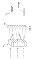
- FIG. 10 illustrates a two-dimensional array of lenslets 1002 .
- the orientation of two-dimensional array of lenslets 1002 in relationship to the optical axis, the scan direction, and the cross-scan direction of lithography device 200 is shown by key 1001 .
- Two-dimensional array of lenslets 1002 can be formed, for example, from a plurality of one-dimensional arrays of lenslets. Typically, each one-dimensional array of lenslets will have different optical properties. Electromagnetic energy is passed through a particular one-dimension array of lenslets, as shown in FIG. 10, which is selected from the plurality of one-dimensional arrays of lenslets that make up the two-dimensional array. Each one-dimensional array of lenslets produces electromagnetic energy having a particular angular distribution.
- partial coherence control module 606 controls the selection and positioning of lenslets.
- Partial coherence control module 606 is coupled to optical element 602 (e.g., the lenslets). Partial coherence control module 606 controls, for example, which of the plurality of one-dimensional arrays of lenslets is positioned to illuminate optical element 604 .
- a memory 608 is coupled to partial coherence control module 606 . Memory 608 stores, for example, data needed to select among the plurality of one-dimensional arrays of lenslets and position the selected one-dimensional array proximate to optical element 604 .
- Partial coherence control module 606 can implement open or closed loop controls. In embodiments, partial coherence control module 606 is implemented using a micro-controller.
- each of the lenslets that makeup a two-dimensional array of lenslets can be individually selected and used to control the angular distribution of electromagnetic energy incident upon first optical element 604 . This can be accomplished, for example, by controlling each row of lenslets of the two-dimensional array of lenslets 1002 individually, rather than collectively, to position a particular lenslet of a row proximate to optical element 604 .
- each row of the two-dimensional array contains lenslets that produce varying degrees of electromagnetic energy spread. The lenslets having the desired or demanded spread, are actively switched (i.e., positioned) into the optical or illumination path of lithography device 300 so that they can be used to illuminate optical element 604 .
- lenslet 1004 can be switch into the illumination path for lenslet 1006 . How to accomplish this switching will be understood by persons skilled in the relevant art given the description herein.
- a partial coherence control module 606 coupled to a memory 608 controls the selection and positioning of individual lenslets.
- optical element 602 comprises a diffractive element or optic. How diffractive elements or optics operate are understood by persons skilled in the relevant optical art. Any suitable diffractive element can be used in accordance with the invention.
- diffractive elements can be formed, for example, from an array of smaller diffractive elements.
- embodiments of the invention that use diffractive elements exhibit all of the advantages and features of the invention described above for embodiments having lenslets. Similar to lenslets, rows or columns of diffractive elements can be built up to vary the angular distribution of the electromagnetic energy used to illuminate optical element 604 . These rows or columns can be adjusted, switched, or positioned similar to lenslets.
- FIGS. 11A and 11B illustrate a flowchart of the steps of a method 1100 for controlling the angular distribution of electromagnetic energy in a lithography device as a function of field position according to an embodiment the invention. The steps of method 1100 will now be described.
- electromagnetic energy is emitted from an illumination source.
- the emitted electromagnetic energy e.g., light
- the emitted electromagnetic energy can be either a continuous source of electromagnetic energy or a pulsed source of electromagnetic energy.
- a pulsed laser operating in a range from about one kilohertz to about four kilohertz is used.
- electromagnetic energy emitted from the illumination source passes through an illumination optics module.
- This illumination optics module includes a partial coherence adjuster module.
- the partial coherence adjuster module includes a replaceable or adjustable optical element, such as optical element 602 , and a customized or standardized optical element, such as optical element 604 .
- the purpose of the optics module is to condition the electromagnetic energy so that is can be used to illuminate a reticle or mask and image a circuit pattern on a wafer.
- the first optical element such as optical element 604
- the second optical element such as optical element 602
- the first and second optical elements can compensate for any imperfections that cause horizontal line and vertical line biases.
- the combination of optical elements can be used to compensate for time-varying phenomena that cause horizontal line and vertical line biases.
- step 1130 electromagnetic energy from the illumination optics module passes through a mask region in a reticle stage.
- the mask region of the reticle stage holds a reticle or mask.
- a circuit pattern thereon is transferred to a photosensitive substrate of a wafer.
- step 1140 electromagnetic energy that passes through the mask region in the reticle stage is imaged, using a projection optics module, to form an image plane proximate to a wafer stage.
- the projection optics module reduces the size of the reticle features transferred to the photosensitive substrate. For example, in an embodiment, the projection optics module reduces the size of the reticle features transferred to the photosensitive substrate by a factor of four.
- the second optical element is adjusted to control the angular distribution of electromagnetic energy at the image plane proximate to the wafer stage.
- the second optical element is adjusted by replacing one or more components (e.g., lenslets) with one or more components having different optical properties.
- the second optical element is adjusted by switching in and out one or more components used to illuminate the first optical element (e.g., lenslets or regions of a diffractive element). This switching can be controlled manually or automatically using one or more open or closed control loops.
Abstract
Description
- The following application of common assignee is related to the present application, and is herein incorporated by reference in its entirety:
- “System and Method for Improving Linewidth Control in a Lithography Device by Varying the Angular Distribution of Light in an Illuminator as a Function of Field Position,” Ser. No. (to be determined), filed on the same day herewith.
- This invention relates to photolithography. More particularly, it relates to line width control in a photolithography device.
- Lithography is used in the manufacture of semiconductor chips. Lithography, or more particularly photolithography, involves projecting one or more images of a reticle or semiconductor circuit mask onto a photosensitive substrate of a wafer. The wafer is then processed to form one or more circuits. As the art of semiconductor chip manufacturing progresses and the size of semiconductor devices become smaller, there is a need for improving line width control in photolithography devices.
- Large semiconductor chips are typically manufactured using a step-and scan lithography device. A step-and-scan lithography device operates by scanning a typically rectangular illumination field defined by an illumination system over a reticle having a circuit pattern thereon. A step-and-scan lithography device is used to manufacture large semiconductor chips, in part, because the size of a semiconductor chip that can be manufactured using a step-and-scan lithography device is not limited to the size of the device's projection optics.
- A method and system for improving line width control, for example, in a step-and-scan lithography device, is described by McCullough et al. in U.S. application Ser. No. 09/599,383, filed Jun. 22, 2000, “Illumination System With Spatially Controllable Partial Coherence Compensating For Linewidth Variances In A Photolithography System,” which is incorporated in its entirety herein by reference. McCullough et al. describe using a custom-designed optical element, such as a microlens array or a diffractive optical element, to control the partial coherence of an illumination system of a lithography device and thereby compensate for line width variances in the lithography device. The custom-designed optical element described by McCullough et al. is designed to compensate for predetermined horizontal and vertical biases associated with a particular lithography device. A limitation of the method of McCullough et al., however, is that it is typically an expensive and time-consuming process to design and manufacture the custom-designed optical element described by McCullough et al. Thus, the custom-designed optical element described by McCullough et al. cannot be readily adjusted, for example, as the horizontal and vertical biases associated with a particular lithography device change with time.
- Other types of lithography devices such as step-and-repeat lithography devices and field-stitching lithography devices also exhibit horizontal and vertical biases that cause line width variances. Compensating for the horizontal and vertical biases in these lithography devices and improving line width control is just as important as compensating for horizontal and vertical biases and improving line width control in a step-and-scan lithography device.
- What is needed is a system and method for controlling line width variations in a lithography device that overcomes the limitations described above.
- The present invention provides a system and method for controlling line width variances in a lithography device. Electromagnetic energy is emitted from an illumination source. A portion of the emitted electromagnetic energy passes through an illumination optics module. The illumination optics module includes a partial coherence adjuster module having a first and a second optical element. These two optical elements are used together to vary the partial coherence of electromagnetic energy emitted by the illumination source, as a function of illumination field position. These two optical elements thereby control line width variances, including time varying variances, in the lithography device.
- In an embodiment, the lithography device includes a reticle stage, a projection optics module, and a wafer stage. The reticle stage is positioned adjacent to the illumination optics module such that electromagnetic energy exiting the illumination optics module will illuminate a portion of a reticle held by the reticle stage. The projection optics module is optically located between the reticle stage and the wafer stage. Electromagnetic energy passing through a reticle held by the reticle stage will enter the projection optics module and be imaged by the projection optics module on a photosensitive substrate, such as a wafer held by the wafer stage.
- In an embodiment, the first optical element is a standard optical element designed to compensate for horizontal and vertical biases associated with lithography devices of a particular make and model. This standard optical element is not customized based on the horizontal and vertical biases associated with a particular lithography device. The second optical element is used for making any changes in the angular distribution of electromagnetic energy incident upon the first optical element needed to compensate for horizontal and vertical biases associated with a particular lithography device.
- In another embodiment, the first optical element is a custom optical element designed to compensate for predetermined horizontal and vertical biases associated with a particular lithography device. This custom optical element is not intended to be interchangeable in other lithography devices. In this embodiment, the second optical element is used for making relatively minor changes in the angular distribution of electromagnetic energy incident upon the first optical element and thereby compensate for any changes in horizontal and vertical biases associated with a particular lithography device.
- In an embodiment, the second optical element is made up of a set of lenslets. These lenslets can be arranged, for example, as a one-dimensional array of lenslets or as a two-dimensional array of lenslets. These lenslets can be replaced and/or repositioned in order to vary the angular distribution of electromagnetic energy incident upon the first optical element.
- In an embodiment, a two-dimensional array of lenslets is formed from a plurality of one-dimensional arrays of lenslets. Each one-dimensional array of lenslets has different optical properties. Electromagnetic energy is passed through a particular one-dimension array of lenslets, selected from the plurality of one-dimensional arrays of lenslets, in order to produce electromagnetic energy having a particular angular distribution.
- In an embodiment, each of the lenslets that makeup the two-dimensional array of lenslets can be individually selected and used to control the angular distribution of electromagnetic energy incident upon said second optical element.
- In an embodiment, a coherence control module is used for selecting among the lenslets. A memory, coupled to the coherence control module, is used for storing data needed to select among the lenslets.
- In another embodiment of the invention, the second optical element is a diffractive optic. This diffractive optic can be replaced by other diffractive optics having different optical properties in order to vary the angular distribution of incident electromagnetic energy.
- Further features and advantages of the present invention, as well as the structure and operation of various embodiments of the present invention, are described in detail below with reference to the accompanying drawings.
- The present invention is described with reference to the accompanying figures. The accompanying figures, which are incorporated herein and form part of the specification, illustrate the present invention and, together with the description, further serve to explain the principles of the invention and to enable a person skilled in the relevant art to make and use the invention. In the figures, like reference numbers indicate identical or functionally similar elements. Additionally, the leftmost digit or digits of a reference number identify the figure in which the reference number first appears.
- FIG. 1 illustrates an example lithography device that incorporates the invention.
- FIG. 2 illustrates how to measure the partial coherence of the lithography device of FIG. 1.
- FIG. 3 illustrates the angular distribution of light in a conventional lithography device as a function of field position.
- FIG. 4A illustrates an unbiased horizontal and an unbiased vertical line formed on a photosensitive substrate.
- FIG. 4B illustrates a biased horizontal and an unbiased vertical line formed on a photosensitive substrate.
- FIG. 4C illustrates an unbiased horizontal and a biased vertical line formed on a photosensitive substrate.
- FIG. 5 illustrates an example relationship between a photosensitive substrate and an illumination field according to the invention.
- FIG. 6 illustrates an example illumination optics module according to the invention.
- FIG. 7 illustrates an example partial coherence adjuster according to an embodiment of the invention.
- FIG. 8 illustrates an example numerical aperture spread of an optical element used to adjust coherence according to an embodiment of the invention.
- FIG. 9 illustrates an example convolved numerical aperture spread of an optical element used to adjust coherence according to an embodiment the invention.
- FIG. 10 illustrates a second example partial coherence adjuster according to an embodiment of the invention.
- FIGS. 11A-B illustrate a flowchart of a method for controlling the angular distribution of electromagnetic energy in a lithography device as a function of field position according to an embodiment the invention.
- The present invention provides a system and method for improving linewidth control in a lithography device. As will be apparent from the detailed description herein, the present invention is particularly well adapted for use with a step-and-scan lithography device.
- In the description that follows, reference will be made in detail to present embodiments of the invention, examples of which are illustrated in the accompanying drawings. While the invention will be described in conjunction with the present embodiments, it will be understood that they are not intended to limit the invention to just these embodiments. On the contrary, the invention is intended to cover alternatives, modifications and equivalents, which can be included within the spirit and scope of the invention as defined by the appended claims. Furthermore, in the following description, for purposes of explanation, numerous specific details are set forth in order to provide a thorough understanding of the present invention. It will be apparent, however, to one skilled in the art, upon reading this disclosure, that the present invention can be practiced without these specific details. In other instances, well-known structures and devices are not described in detail in order to avoid obscuring aspects of the present invention.
- Terminology
- The following terms are defined so that they may be used to describe embodiments of the present invention. As used herein:
- “Adjustable Optical Element” means one or more optical components such as, for example, lenslets or gratings that can be changed, either automatically or manually, in order to bring about a change of partial coherence. A group of lenslets that can be switched into and out of an illumination path of a lithography device is an example of an adjustable optical element.
- “Customized Optical Element” means an optical element specifically as designed to compensate for the optical characteristics of a particular lithography device. Customized optical elements are not intended to be used in a lithography device other than the one for which it is specifically designed.
- “Diffractive element” or “diffractive optic” means a device capable of causing diffraction of electromagnetic energy. Diffractive optics include transmission gratings and reflection gratings.
- “Illumination source” means any source of illumination such as, for example, a continuous or pulsed laser that is suitable for performing lithography.
- “Lithography device” means any lithography device to include a step-and-scan lithography device, a step-and-repeat lithography device, and/or a field-stitching lithography device, unless otherwise noted.
- “Positioned adjacent to” means a first module or device is positioned relative to a second module or device so that electromagnetic energy exiting the first module or device will enter the second module or device, either directly or indirectly. The phrase “positioned adjacent to” includes instances where one or more optical elements are used to direct electromagnetic energy exiting the first module or device into the second module or device.
- “Replaceable Optical Element” means one or more optical components such as, for example, lenslets or gratings that can be replace by one or more optical components in order to bring about a change of partial coherence. A group of lenslets or a grating that can be replaced by another group of lenslets or another grating, having different optical properties, is an example of a replaceable optical element.
- “Reticle stage” means that portion of a lithography device used to hold and position a reticle or semiconductor mask.
- “Standardized Optical Element” means an optical element designed to compensate for the optical characteristics particular to a specific make or model of a lithography device. Standardized optical elements are intended to be used interchangeably in all lithography devices conforming to a specific make or model.
- “Wafer” or “Photosensitive Substrate” both mean a wafer having a photosensitive coating of the type used by semiconductor manufacturers to produce semiconductor chips.
- “Wafer stage” means that portion of a lithography device used to hold and position a wafer.
- System Embodiments of the Invention
- FIG. 1 illustrates an
example lithography device 100 that embodies the invention. Anillumination source 102 generates and directs electromagnetic energy into anillumination optics module 104.Illumination optics module 104 includes a partialcoherence adjuster module 105 that conditions the electromagnetic energy received fromillumination source 102 in accordance with the invention. Conditioned electromagnetic energy leavesillumination optics module 104 and passes through a reticle (not shown) held by areticle stage 106. The reticle is used to project an image of a circuit onto a wafer orphotosensitive substrate 110. Electromagnetic energy passing through the reticle enters aprojection optics module 108.Projection optics module 108 images the received electromagnetic energy onphotosensitive substrate 110.Photosensitive substrate 110 is held and moved by awafer stage 112. Astage control 114 controls the position ofreticle stage 106 andwafer stage 112, thereby controlling the position of the reticle (not shown) andphotosensitive substrate 110. -
Illumination source 102 comprises a source of electromagnetic energy.Illumination source 102 can be either a continuous source of electromagnetic energy or a pulsed source of electromagnetic energy. For example, a pulsed laser operating in a range from about one kilohertz to about four kilohertz can be used. As will be understood by a person skilled in the relevant lithography art, the electromagnetic energy produced byillumination source 102 requires conditioning before it is used to exposephotosensitive substrate 110. -
Illumination optics module 104 comprises optical elements that condition the electromagnetic energy received fromillumination source 102. Optical elements that form a part ofillumination optics module 104 are described below and, for example, in U.S. Pat. No. 5,631,721 to Stanton et. al., which is herein incorporated by reference in its entirety. In particular,illumination optics module 104 contains apartialcoherence adjuster module 105. Partialcoherence adjuster module 105 contains optical elements for varying the angular distribution of electromagnetic energy emitted byillumination source 102 as a function of field position (e.g., for varying the angular distribution of electromagnetic energy ofillumination field 312, as described below). In embodiments, partialcoherence adjuster module 105 contains a customized or standardized optical element and either a set of lenslets or a diffractive optic for varying the angular distribution of electromagnetic energy emitted byillumination source 102 as a function of illumination field position. These features of the invention are described below in more detail. - Electromagnetic energy exiting
illumination optics module 104 is used to illuminate a reticle (not shown) held byreticle stage 106. By illuminating the reticle, a circuit pattern thereon is transferred tophotosensitive substrate 110.Photosensitive substrate 110 is processed in a manner known to persons skilled in the lithography arts to form one or more circuits. -
Projection optics module 108 is used to image electromagnetic energy that passes through the reticle ontophotosensitive substrate 110.Projection optics 108 can also be used to reduce the reticle image formed onphotosensitive substrate 110. -
Stage control 114 controls the movement and positioning ofreticle sage 106 andwafer stage 112.Stage control 114 enableslithography device 100 to operate in either a step-and-scan mode, a step-and-repeat mode, and/or a field stitching mode. - FIG. 2 illustrates how to measure the partial coherence of
lithography device 100. Twocones 208 and 210 are shown in FIG. 2.Cone 210 represents the actual space through which electromagnetic energy fromillumination source 102 passes to illuminate a reticle held byreticle stage 106. Cone 208 represents the maximum cone or space through which electromagnetic energy can pass and still be used to imagewafer 110. The angular distribution of cone 210 (i.e., the partial coherence factor σ of cone 210) is given by EQ. 1:
- where, as shown in FIG. 2, cone 208 forms an angle θm with a optical axis of
lithography device 100, andcone 210 forms an angle θ0 with the optical axis. - FIG. 3 illustrates the angular distribution of light in a
conventional lithography device 300 as a function of field position. In FIG. 3, electromagnetic energy is shown exiting anillumination optics module 302. This exiting electromagnetic energy has not been conditioned in accordance with the invention. The exiting electromagnetic energy passes through areticle stage 304. A reticle or semiconductor mask (not shown) is placed at an image plan ofreticle stage 304. The exiting electromagnetic energy passes through aprojection optics module 306.Projection optics module 306 images electromagnetic energy at an image plane located proximate to a wafer stage. - As illustrated in FIG. 3, the electromagnetic energy exiting
illumination optics module 302 forms cones of electromagnetic energy (see, e.g.,cone 310A). Similar cones of electromagnetic energy (see, e.g.,cone 310B) are also formed by the electromagnetic energy as it exitsprojection optics module 306. These cones of electromagnetic energy (represented ascones illumination field 312.Illumination field 312 is used to expose a photosensitive substrate of awafer 330. -
Illumination field 312 does not vary as a function of field position. Each cone of electromagnetic (e.g., 310B, 314, 316, 318, and 320) that forms a part ofillumination field 312 exposes a different point onwafer 330.Cone 308B illustrates a maximum cone of electromagnetic energy that can be used to expose the photosensitive substrate ofwafer 330. This cone is also shown ascone 308A. The shape (i.e., cross-sectional view) of each cone of electromagnetic (e.g., 310B, 314, 316, 318, and 320) is intended to represent the partial coherence of the electromagnetic energy at a particular point inillumination field 312. - As shown in FIG. 3, there is a relationship between the
cones cone 310A causes a similar change to be brought about incone 310B.Cones lithography device 300. - FIGS. 4A, 4B, and 4C illustrate horizontal line and vertical line biases. These line biases are brought about, for example, by imperfections in reticles and the optics of a conventional lithography device such as
lithography device 300. - FIG. 4A illustrates an unbiased
horizontal line 402 having a width WH and an unbiasedvertical line 404 having a width WV formed onwafer 330. - FIG. 4B illustrates a biased
horizontal line 406 having a width WH′ and an unbiasedvertical line 404 having a width WV formed onwafer 330. - FIG. 4C illustrates an unbiased
horizontal line 402 having a width WH and a biasedvertical line 408 having a width WV′ formed onwafer 330. - As will become apparent to persons skilled in the relevant lithography art given the description herein, the present invention can be used to control the angular distribution or partial coherence of the electromagnetic energy in
illumination field 312, as a function of field position, and thereby improve the performance oflithography device 300. By varying the partial coherence of the electromagnetic energy used to expose wafer 330 (e.g., the shape ofcones wafer 330 are reduced. Embodiments of the invention are also used improve the performance of lithography devices other thanlithography device 300 that use, for example, a square or an annular slit illumination field to expose a wafer. - FIG. 5 illustrates the relationship between
wafer 330 andillumination field 312. FIG. 5 also illustrates how the invention can be used to vary the partial coherence of the electromagnetic energy used to expose wafer 330 (see, e.g., the shape ofcones wafer 330. - As illustrated in FIG. 5,
illumination field 312 is used to expose ascan area 502 ofwafer 330. The partial coherence or angular distribution of electromagnetic energy inillumination field 312 varies as a function of field position. Each point ofwafer 330 can be exposed differently along the length ofillumination field 312 as illumination filed 312 scans acrossscan area 502.Illumination cones - FIG. 6 further illustrates
illumination optics module 104 according to an embodiment of the invention.Illumination optics module 104 includes partialcoherence adjuster module 105, anillumination field delimiter 610, andoptical elements 620. As described herein,electromagnetic energy 601 entersillumination optics module 104 fromillumination source 102. Partialcoherence adjuster module 105 is used to adjust the partial coherence ofelectromagnetic energy 601 as a function of illumination field position (e.g., illumination field 312) and thereby transformelectromagnetic energy 601 intoelectromagnetic energy 631.Electromagnetic energy 631 exitsilluminations optics module 104 towardsreticle stage 106. - As shown in FIG. 6, partial
coherence adjuster module 105 includes an adjustable or replaceableoptical element 602 and a customized or standardizedoptical element 604.Optical element 604 is used for changing the partial coherence of incident electromagnetic energy in a predetermined manner to compensate for horizontal and vertical line biases.Optical element 602 is used for changing the angular distribution of electromagnetic energy incident uponoptical element 604. In embodiments of the invention,optical element 602 comprises a set of lenslets. In other embodiments,optical element 602 comprises an array of diffractive optics. - A customized or standardized
optical element 604 is used to modify the partial coherence of electromagnetic energy emitted byillumination source 102.Optical element 604 comprises, for example, micro lenses or diffractive elements that change the partial coherence of the electromagnetic energy incident uponoptical element 604.Optical element 604 is designed to compensate for changes in the partial coherence of electromagnetic energy brought about, for example, by imperfections inprojection optics module 108 that lead to horizontal and vertical line width biases. - A customized
optical element 604 is described in detail in U.S. patent application Ser. No. 09/599,383 by McCullough et al. - Designing
optical element 604 to compensate for the average or typical imperfections of a particular model of lithography devices has many advantages. For example, it reduces production costs and production time. When used in combination,optical elements optical element 602, the combination ofoptical elements - As will be understood by a person skilled in the relevant lithography art given the description herein, the design of the
optical elements - In embodiments of the invention,
optical element 602 is adjusted based on detected variations in printed line widths formed on a photosensitive substrate (wafer 110) held bywafer stage 112. The detected variations in printed line widths can be compared to the reticle used to expose the photosensitive substrate, and the appropriate adjustments needed to reduce the variations in line widths for the reticle determined. In other embodiments,optical element 602 is adjusted based on detected variations in time-varying parameters. Time-varying parameters that may cause linewidth variations include temperature, pressure, and resist being used. Other time-varying parameters are known to persons skilled in the relevant lithography art. This detection and analysis process can be done on a continuous real-time basis, or it can be done periodically (e.g., from time-to-time). - As shown in FIG. 6, some embodiments of the invention include an optional partial
coherence control module 606 and anoptional memory 608. The purpose and function of these devices is described below with regard to the embodiment of the invention illustrated in FIG. 10. -
Illumination field delimiter 610 is used to set the maximum size and shape of the illumination field used to exposewafer 330. In embodiments of the invention, the size and shape of the illumination field formed bydelimiter 610 is controlled by an optional scanningfield control module 612 and anoptional memory 614. This feature is used, for example, to control the amount of electromagnetic energy used to image a particular reticle. -
Optical elements 620 represent additional reflective and/or refractive optical elements used to route and/or condition the electromagnetic energy. The optical elements that form a part ofoptical elements 620 are known to persons skilled in the relevant art. - As described herein, in embodiments of the invention,
optical element 602 is formed using lenslets. FIG. 7 illustrates an embodiment where a set of lenslets are arranged as a one-dimensional array oflenslets 702. The orientation of one-dimensional array oflenslets 702 in relationship to the optical axis, the scan direction, and the cross-scan direction oflithography device 300 is shown bykey 701.Lenslets lenslets 702. Electromagnetic energy entering one-dimensional array oflenslets 702 is spread by the individual lenslets over customized or standardizedoptical element 604. More particularly, the lenslets of the array control the incident angle of the electromagnetic energy at any point onoptical element 604 in order to control the exiting angular distribution of electromagnetic energy fromoptical element 604. The effect is to convolve the numerical aperture fromoptical element 604 with that ofoptical element 602, and thereby increase the overall numerical aperture of partialcoherence adjuster module 105. - FIG. 8 illustrates an example numerical aperture spread from
optical element 604, in a cross-scan direction of a step-and scan lithography device, when illuminated with collimated electromagnetic energy (e.g., when no lenslets are present). - FIG. 9 illustrates an example convolved numerical aperture spread from
optical element 604, in a cross-scan direction of a step-and scan lithography device, when illuminated according to the invention (e.g., when lenslets are present). - As will be understood by a person skilled in the relevant art given the description herein, the spread of the electromagnetic energy exiting one-dimensional array of
lenslets 702 is determined by the optical properties of all the individual lenslets of the array. Thus, by changing at least one lenslet of the array, one can vary or control the angular distribution or coherence of the electromagnetic energy exitingoptical element 604. By changing the lenslets, or the entire array, one can compensate for time-varying phenomena that cause horizontal line and vertical line biases. - In embodiments of the invention, the set of lenslets that makeup
optical element 602 is arranged as a two-dimensional array of lenslets. This arrangement has many advantages. - FIG. 10 illustrates a two-dimensional array of
lenslets 1002. The orientation of two-dimensional array oflenslets 1002 in relationship to the optical axis, the scan direction, and the cross-scan direction of lithography device 200 is shown by key 1001. Two-dimensional array oflenslets 1002 can be formed, for example, from a plurality of one-dimensional arrays of lenslets. Typically, each one-dimensional array of lenslets will have different optical properties. Electromagnetic energy is passed through a particular one-dimension array of lenslets, as shown in FIG. 10, which is selected from the plurality of one-dimensional arrays of lenslets that make up the two-dimensional array. Each one-dimensional array of lenslets produces electromagnetic energy having a particular angular distribution. - In embodiments of the invention, partial
coherence control module 606 controls the selection and positioning of lenslets. Partialcoherence control module 606 is coupled to optical element 602 (e.g., the lenslets). Partialcoherence control module 606 controls, for example, which of the plurality of one-dimensional arrays of lenslets is positioned to illuminateoptical element 604. In embodiments, amemory 608 is coupled to partialcoherence control module 606.Memory 608 stores, for example, data needed to select among the plurality of one-dimensional arrays of lenslets and position the selected one-dimensional array proximate tooptical element 604. Partialcoherence control module 606 can implement open or closed loop controls. In embodiments, partialcoherence control module 606 is implemented using a micro-controller. - In embodiments, each of the lenslets that makeup a two-dimensional array of lenslets can be individually selected and used to control the angular distribution of electromagnetic energy incident upon first
optical element 604. This can be accomplished, for example, by controlling each row of lenslets of the two-dimensional array oflenslets 1002 individually, rather than collectively, to position a particular lenslet of a row proximate tooptical element 604. In an embodiment, each row of the two-dimensional array contains lenslets that produce varying degrees of electromagnetic energy spread. The lenslets having the desired or demanded spread, are actively switched (i.e., positioned) into the optical or illumination path oflithography device 300 so that they can be used to illuminateoptical element 604. For example,lenslet 1004 can be switch into the illumination path forlenslet 1006. How to accomplish this switching will be understood by persons skilled in the relevant art given the description herein. In a manner similar to that described above, in embodiments of the invention, a partialcoherence control module 606 coupled to amemory 608 controls the selection and positioning of individual lenslets. - In embodiments,
optical element 602 comprises a diffractive element or optic. How diffractive elements or optics operate are understood by persons skilled in the relevant optical art. Any suitable diffractive element can be used in accordance with the invention. - As will be understood by a person skilled in the relevant art given the description herein, diffractive elements can be formed, for example, from an array of smaller diffractive elements. Thus, embodiments of the invention that use diffractive elements exhibit all of the advantages and features of the invention described above for embodiments having lenslets. Similar to lenslets, rows or columns of diffractive elements can be built up to vary the angular distribution of the electromagnetic energy used to illuminate
optical element 604. These rows or columns can be adjusted, switched, or positioned similar to lenslets. - Method Embodiment of the Invention
- FIGS. 11A and 11B illustrate a flowchart of the steps of a method 1100 for controlling the angular distribution of electromagnetic energy in a lithography device as a function of field position according to an embodiment the invention. The steps of method 1100 will now be described.
- In
step 1110, electromagnetic energy is emitted from an illumination source. The emitted electromagnetic energy (e.g., light) can be either a continuous source of electromagnetic energy or a pulsed source of electromagnetic energy. In an embodiment, a pulsed laser operating in a range from about one kilohertz to about four kilohertz is used. - In
step 1120, electromagnetic energy emitted from the illumination source passes through an illumination optics module. This illumination optics module includes a partial coherence adjuster module. The partial coherence adjuster module includes a replaceable or adjustable optical element, such asoptical element 602, and a customized or standardized optical element, such asoptical element 604. As noted herein, the purpose of the optics module is to condition the electromagnetic energy so that is can be used to illuminate a reticle or mask and image a circuit pattern on a wafer. - As described herein, the first optical element, such as
optical element 604, changes the partial coherence of incident electromagnetic energy in a predetermined manner to compensate for horizontal and vertical line biases. The second optical element, such asoptical element 602, changes the angular distribution of electromagnetic energy incident upon the first optical element. When used in combination, the first and second optical elements can compensate for any imperfections that cause horizontal line and vertical line biases. By adjusting the second optical element, or replacing it with another optical element according to the invention, the combination of optical elements can be used to compensate for time-varying phenomena that cause horizontal line and vertical line biases. - In
step 1130, electromagnetic energy from the illumination optics module passes through a mask region in a reticle stage. In operation, the mask region of the reticle stage holds a reticle or mask. By illuminating the reticle, a circuit pattern thereon is transferred to a photosensitive substrate of a wafer. - In
step 1140, electromagnetic energy that passes through the mask region in the reticle stage is imaged, using a projection optics module, to form an image plane proximate to a wafer stage. In embodiments, the projection optics module reduces the size of the reticle features transferred to the photosensitive substrate. For example, in an embodiment, the projection optics module reduces the size of the reticle features transferred to the photosensitive substrate by a factor of four. - In
step 1150, the second optical element is adjusted to control the angular distribution of electromagnetic energy at the image plane proximate to the wafer stage. In an embodiment, the second optical element is adjusted by replacing one or more components (e.g., lenslets) with one or more components having different optical properties. In other embodiments, the second optical element is adjusted by switching in and out one or more components used to illuminate the first optical element (e.g., lenslets or regions of a diffractive element). This switching can be controlled manually or automatically using one or more open or closed control loops. - As will be understood by a person skilled in the relevant lithography art, there are many factors that can be used to determine how, for example, the lenslets or diffractive elements used to vary the angular distribution of the electromagnetic energy incident on the first optical element should be adjusted in order to improve line width control in accordance with the invention. Thus, the factors discussed herein have been presented by way of example only, and not limitation.
- Conclusion
- Various embodiments of the present invention have been described above. It should be understood that these embodiments have been presented by way of example only, and not limitation. It will be understood by those skilled in the relevant art that various changes in form and details of the embodiments described above may be made without departing from the spirit and scope of the present invention as defined in the claims. Thus, the breadth and scope of the present invention should not be limited by any of the above-described exemplary embodiments, but should be defined only in accordance with the following claims and their equivalents.
Claims (35)
Priority Applications (7)
| Application Number | Priority Date | Filing Date | Title |
|---|---|---|---|
| US10/127,506 US6784976B2 (en) | 2002-04-23 | 2002-04-23 | System and method for improving line width control in a lithography device using an illumination system having pre-numerical aperture control |
| TW092108965A TWI299880B (en) | 2002-04-23 | 2003-04-17 | System and method for improving line width control in a lithography device using an illumination system having pre-numerical aperture control |
| CNB031222366A CN1307485C (en) | 2002-04-23 | 2003-04-23 | System and method for improving line width control in use of photoetching apparatus of illuminating system with prenumerical value aperture control |
| KR1020030025724A KR100773995B1 (en) | 2002-04-23 | 2003-04-23 | Device and method for improving line width control in a lithography device using an illumination system having pre-numerical aperture control |
| SG200302351A SG116490A1 (en) | 2002-04-23 | 2003-04-23 | System and method for improving line width controlin a lithography device using an illumination system having pre-numerical aperture control. |
| JP2003118993A JP2003318106A (en) | 2002-04-23 | 2003-04-23 | Lithography system and method for controlling angular distribution of electromagnetic energy in lithography device as function of illumination field position |
| EP03008808A EP1357431A3 (en) | 2002-04-23 | 2003-04-23 | System and method for improving line width control in a lithography device using an illumination system having pre-numerical aperture control |
Applications Claiming Priority (1)
| Application Number | Priority Date | Filing Date | Title |
|---|---|---|---|
| US10/127,506 US6784976B2 (en) | 2002-04-23 | 2002-04-23 | System and method for improving line width control in a lithography device using an illumination system having pre-numerical aperture control |
Publications (2)
| Publication Number | Publication Date |
|---|---|
| US20030197846A1 true US20030197846A1 (en) | 2003-10-23 |
| US6784976B2 US6784976B2 (en) | 2004-08-31 |
Family
ID=28790942
Family Applications (1)
| Application Number | Title | Priority Date | Filing Date |
|---|---|---|---|
| US10/127,506 Expired - Lifetime US6784976B2 (en) | 2002-04-23 | 2002-04-23 | System and method for improving line width control in a lithography device using an illumination system having pre-numerical aperture control |
Country Status (7)
| Country | Link |
|---|---|
| US (1) | US6784976B2 (en) |
| EP (1) | EP1357431A3 (en) |
| JP (1) | JP2003318106A (en) |
| KR (1) | KR100773995B1 (en) |
| CN (1) | CN1307485C (en) |
| SG (1) | SG116490A1 (en) |
| TW (1) | TWI299880B (en) |
Cited By (4)
| Publication number | Priority date | Publication date | Assignee | Title |
|---|---|---|---|---|
| US20030197842A1 (en) * | 2002-04-23 | 2003-10-23 | Asml Us, Inc. | System and method for improving linewidth control in a lithography device by varying the angular distribution of light in an illuminator as a function of field position |
| US20050078292A1 (en) * | 2003-08-29 | 2005-04-14 | Asml Netherlands B.V. | Lithographic apparatus, device manufacturing method, and device manufactured thereby |
| US20070242253A1 (en) * | 2006-04-13 | 2007-10-18 | Asml Netherlands B.V. | Moving beam with respect to diffractive optics in order to reduce interference patterns |
| US8081295B2 (en) | 2005-03-15 | 2011-12-20 | Carl Zeiss Smt Gmbh | Projection exposure method and projection exposure system therefor |
Families Citing this family (8)
| Publication number | Priority date | Publication date | Assignee | Title |
|---|---|---|---|---|
| US6842223B2 (en) | 2003-04-11 | 2005-01-11 | Nikon Precision Inc. | Enhanced illuminator for use in photolithographic systems |
| US7934172B2 (en) | 2005-08-08 | 2011-04-26 | Micronic Laser Systems Ab | SLM lithography: printing to below K1=.30 without previous OPC processing |
| US20090213354A1 (en) * | 2005-08-08 | 2009-08-27 | Micronic Laser Systems Ab | Method and apparatus for projection printing |
| KR100712997B1 (en) * | 2005-09-30 | 2007-05-02 | 주식회사 하이닉스반도체 | Exposure system for controlling the vertical/horizontal CD difference and method of photolithography using the exposure system |
| EP2649493A1 (en) * | 2010-08-30 | 2013-10-16 | Carl Zeiss SMT GmbH | Illumination system of a microlithographic projection exposure apparatus |
| JP6016169B2 (en) | 2011-01-29 | 2016-10-26 | カール・ツァイス・エスエムティー・ゲーエムベーハー | Illumination system of microlithographic projection exposure apparatus |
| KR101658985B1 (en) | 2015-01-30 | 2016-09-23 | 한국기계연구원 | Optical Layout Apparatus for Lithography |
| KR20180010242A (en) * | 2015-05-21 | 2018-01-30 | 칼 짜이스 에스엠티 게엠베하 | Method of operating a microlithographic projection apparatus |
Citations (14)
| Publication number | Priority date | Publication date | Assignee | Title |
|---|---|---|---|---|
| US4988188A (en) * | 1987-08-31 | 1991-01-29 | Canon Kabushiki Kaisha | Illumination device |
| US5296892A (en) * | 1992-02-01 | 1994-03-22 | Nikon Corporation | Illuminating apparatus and projection exposure apparatus provided with such an illuminating apparatus |
| US5329336A (en) * | 1992-07-06 | 1994-07-12 | Nikon Corporation | Exposure method and apparatus |
| US5357312A (en) * | 1992-10-01 | 1994-10-18 | Nec Corporation | Illuminating system in exposure apparatus for photolithography |
| US5631721A (en) * | 1995-05-24 | 1997-05-20 | Svg Lithography Systems, Inc. | Hybrid illumination system for use in photolithography |
| US5724122A (en) * | 1995-05-24 | 1998-03-03 | Svg Lithography Systems, Inc. | Illumination system having spatially separate vertical and horizontal image planes for use in photolithography |
| US5896188A (en) * | 1996-11-25 | 1999-04-20 | Svg Lithography Systems, Inc. | Reduction of pattern noise in scanning lithographic system illuminators |
| US5895737A (en) * | 1997-03-31 | 1999-04-20 | Svg Lithography Systems, Inc. | Method for adjusting an illumination field based on selected reticle feature |
| US6013401A (en) * | 1997-03-31 | 2000-01-11 | Svg Lithography Systems, Inc. | Method of controlling illumination field to reduce line width variation |
| US6259513B1 (en) * | 1996-11-25 | 2001-07-10 | Svg Lithography Systems, Inc. | Illumination system with spatially controllable partial coherence |
| US20010043318A1 (en) * | 2000-04-03 | 2001-11-22 | Kenichiro Mori | Illumination optical system for use in projection exposure apparatus |
| US20010046038A1 (en) * | 1998-04-08 | 2001-11-29 | Johannes Catharinus H. Mulkens | Lithography apparatus |
| US20020014600A1 (en) * | 2000-07-26 | 2002-02-07 | Kabushiki Kaisha Toshiba | Scanning exposure method |
| US6573975B2 (en) * | 2001-04-04 | 2003-06-03 | Pradeep K. Govil | DUV scanner linewidth control by mask error factor compensation |
Family Cites Families (9)
| Publication number | Priority date | Publication date | Assignee | Title |
|---|---|---|---|---|
| US5383000A (en) * | 1992-11-24 | 1995-01-17 | General Signal Corporation | Partial coherence varier for microlithographic system |
| JP2829252B2 (en) * | 1994-03-07 | 1998-11-25 | 現代電子産業株式会社 | Assembled light beam adjusting device for exposure equipment |
| JP3571397B2 (en) * | 1995-02-20 | 2004-09-29 | シャープ株式会社 | Light source filter, projection exposure apparatus and projection exposure method using the same |
| US6628370B1 (en) * | 1996-11-25 | 2003-09-30 | Mccullough Andrew W. | Illumination system with spatially controllable partial coherence compensating for line width variances in a photolithographic system |
| EP0949541B1 (en) * | 1998-04-08 | 2006-06-07 | ASML Netherlands B.V. | Lithography apparatus |
| WO2000057459A1 (en) * | 1999-03-24 | 2000-09-28 | Nikon Corporation | Exposure method and apparatus |
| JP2001267205A (en) * | 2000-03-15 | 2001-09-28 | Nec Corp | Exposure system |
| JP2002075815A (en) * | 2000-08-23 | 2002-03-15 | Sony Corp | Pattern tester and aligner control system using the same |
| CN1141620C (en) * | 2001-07-26 | 2004-03-10 | 清华大学 | Scanner with array light source for IC photo etching system |
-
2002
- 2002-04-23 US US10/127,506 patent/US6784976B2/en not_active Expired - Lifetime
-
2003
- 2003-04-17 TW TW092108965A patent/TWI299880B/en not_active IP Right Cessation
- 2003-04-23 EP EP03008808A patent/EP1357431A3/en not_active Withdrawn
- 2003-04-23 JP JP2003118993A patent/JP2003318106A/en active Pending
- 2003-04-23 SG SG200302351A patent/SG116490A1/en unknown
- 2003-04-23 KR KR1020030025724A patent/KR100773995B1/en active IP Right Grant
- 2003-04-23 CN CNB031222366A patent/CN1307485C/en not_active Expired - Lifetime
Patent Citations (15)
| Publication number | Priority date | Publication date | Assignee | Title |
|---|---|---|---|---|
| US4988188A (en) * | 1987-08-31 | 1991-01-29 | Canon Kabushiki Kaisha | Illumination device |
| US5296892A (en) * | 1992-02-01 | 1994-03-22 | Nikon Corporation | Illuminating apparatus and projection exposure apparatus provided with such an illuminating apparatus |
| US5329336A (en) * | 1992-07-06 | 1994-07-12 | Nikon Corporation | Exposure method and apparatus |
| US5357312A (en) * | 1992-10-01 | 1994-10-18 | Nec Corporation | Illuminating system in exposure apparatus for photolithography |
| US5631721A (en) * | 1995-05-24 | 1997-05-20 | Svg Lithography Systems, Inc. | Hybrid illumination system for use in photolithography |
| US5724122A (en) * | 1995-05-24 | 1998-03-03 | Svg Lithography Systems, Inc. | Illumination system having spatially separate vertical and horizontal image planes for use in photolithography |
| US5896188A (en) * | 1996-11-25 | 1999-04-20 | Svg Lithography Systems, Inc. | Reduction of pattern noise in scanning lithographic system illuminators |
| US6259513B1 (en) * | 1996-11-25 | 2001-07-10 | Svg Lithography Systems, Inc. | Illumination system with spatially controllable partial coherence |
| US5895737A (en) * | 1997-03-31 | 1999-04-20 | Svg Lithography Systems, Inc. | Method for adjusting an illumination field based on selected reticle feature |
| US5966202A (en) * | 1997-03-31 | 1999-10-12 | Svg Lithography Systems, Inc. | Adjustable slit |
| US6013401A (en) * | 1997-03-31 | 2000-01-11 | Svg Lithography Systems, Inc. | Method of controlling illumination field to reduce line width variation |
| US20010046038A1 (en) * | 1998-04-08 | 2001-11-29 | Johannes Catharinus H. Mulkens | Lithography apparatus |
| US20010043318A1 (en) * | 2000-04-03 | 2001-11-22 | Kenichiro Mori | Illumination optical system for use in projection exposure apparatus |
| US20020014600A1 (en) * | 2000-07-26 | 2002-02-07 | Kabushiki Kaisha Toshiba | Scanning exposure method |
| US6573975B2 (en) * | 2001-04-04 | 2003-06-03 | Pradeep K. Govil | DUV scanner linewidth control by mask error factor compensation |
Cited By (8)
| Publication number | Priority date | Publication date | Assignee | Title |
|---|---|---|---|---|
| US20030197842A1 (en) * | 2002-04-23 | 2003-10-23 | Asml Us, Inc. | System and method for improving linewidth control in a lithography device by varying the angular distribution of light in an illuminator as a function of field position |
| US6888615B2 (en) * | 2002-04-23 | 2005-05-03 | Asml Holding N.V. | System and method for improving linewidth control in a lithography device by varying the angular distribution of light in an illuminator as a function of field position |
| US20050078292A1 (en) * | 2003-08-29 | 2005-04-14 | Asml Netherlands B.V. | Lithographic apparatus, device manufacturing method, and device manufactured thereby |
| US7230678B2 (en) * | 2003-08-29 | 2007-06-12 | Asml Netherlands B.V. | Lithographic apparatus, device manufacturing method, and device manufactured thereby |
| US8081295B2 (en) | 2005-03-15 | 2011-12-20 | Carl Zeiss Smt Gmbh | Projection exposure method and projection exposure system therefor |
| US9110383B2 (en) | 2005-03-15 | 2015-08-18 | Carl Zeiss Smt Gmbh | Projection exposure method and projection exposure system therefor |
| US20070242253A1 (en) * | 2006-04-13 | 2007-10-18 | Asml Netherlands B.V. | Moving beam with respect to diffractive optics in order to reduce interference patterns |
| US7948606B2 (en) | 2006-04-13 | 2011-05-24 | Asml Netherlands B.V. | Moving beam with respect to diffractive optics in order to reduce interference patterns |
Also Published As
| Publication number | Publication date |
|---|---|
| CN1453643A (en) | 2003-11-05 |
| EP1357431A3 (en) | 2008-10-01 |
| TWI299880B (en) | 2008-08-11 |
| EP1357431A2 (en) | 2003-10-29 |
| KR20040002504A (en) | 2004-01-07 |
| CN1307485C (en) | 2007-03-28 |
| SG116490A1 (en) | 2005-11-28 |
| TW200307983A (en) | 2003-12-16 |
| KR100773995B1 (en) | 2007-11-08 |
| JP2003318106A (en) | 2003-11-07 |
| US6784976B2 (en) | 2004-08-31 |
Similar Documents
| Publication | Publication Date | Title |
|---|---|---|
| US6822728B2 (en) | Illumination system with spatially controllable partial coherence compensation for line width variances in a photolithographic system | |
| EP2188664B1 (en) | Illumination optical system, exposure apparatus, optical element and manufacturing method thereof, and device manufacturing method | |
| JP4324957B2 (en) | Illumination optical apparatus, exposure apparatus, and exposure method | |
| US7095560B2 (en) | Diffractive optical device, refractive optical device, illumination optical system, exposure apparatus and exposure method | |
| US20060181692A1 (en) | Method and apparatus for controlling radiation beam intensity directed to microlithograhic substrates | |
| EP1262836A1 (en) | Lithographic apparatus | |
| US6784976B2 (en) | System and method for improving line width control in a lithography device using an illumination system having pre-numerical aperture control | |
| US7468781B2 (en) | Exposure apparatus | |
| KR102268034B1 (en) | Projection exposure method and projection exposure apparatus for microlithography | |
| US20070024836A1 (en) | Illumination system for a microlithographic projection exposure apparatus | |
| US6888615B2 (en) | System and method for improving linewidth control in a lithography device by varying the angular distribution of light in an illuminator as a function of field position | |
| US6323937B1 (en) | Projection exposure apparatus, and device manufacturing method using the same | |
| JP3200244B2 (en) | Scanning exposure equipment | |
| US6707537B2 (en) | Projection exposure system | |
| JP2004266259A (en) | Illumination optical device, exposure apparatus, and exposure method | |
| JPH08203807A (en) | Projection exposure system | |
| KR20060126682A (en) | Illumination system for a microlithographic projection exposure apparatus | |
| JPH08255739A (en) | Aligner | |
| JPH08203813A (en) | Scanning projection aligner |
Legal Events
| Date | Code | Title | Description |
|---|---|---|---|
| AS | Assignment |
Owner name: ASML US, INC., CONNECTICUT Free format text: ASSIGNMENT OF ASSIGNORS INTEREST;ASSIGNORS:COSTON, SCOTT D.;TSACOYEANES, JAMES G.;REEL/FRAME:012828/0428 Effective date: 20020410 |
|
| AS | Assignment |
Owner name: ASML HOLDING N.V., NETHERLANDS Free format text: ASSIGNMENT OF ASSIGNORS INTEREST;ASSIGNOR:ASML US, INC.;REEL/FRAME:013743/0510 Effective date: 20030521 |
|
| AS | Assignment |
Owner name: ASML US, INC., ARIZONA Free format text: MERGER;ASSIGNOR:ASM LITHOGRAPHY, INC. AND ASML US, LLC;REEL/FRAME:014953/0042 Effective date: 20021231 Owner name: ASML US, LLC, DELAWARE Free format text: CONVERSION;ASSIGNOR:ASML US, INC.;REEL/FRAME:014953/0047 Effective date: 20021004 |
|
| STCF | Information on status: patent grant |
Free format text: PATENTED CASE |
|
| FEPP | Fee payment procedure |
Free format text: PAYOR NUMBER ASSIGNED (ORIGINAL EVENT CODE: ASPN); ENTITY STATUS OF PATENT OWNER: LARGE ENTITY |
|
| FPAY | Fee payment |
Year of fee payment: 4 |
|
| FPAY | Fee payment |
Year of fee payment: 8 |
|
| FPAY | Fee payment |
Year of fee payment: 12 |