US20030197828A1 - Substrate for liquid crystal display - Google Patents
Substrate for liquid crystal display Download PDFInfo
- Publication number
- US20030197828A1 US20030197828A1 US10/329,470 US32947002A US2003197828A1 US 20030197828 A1 US20030197828 A1 US 20030197828A1 US 32947002 A US32947002 A US 32947002A US 2003197828 A1 US2003197828 A1 US 2003197828A1
- Authority
- US
- United States
- Prior art keywords
- line
- substrate
- liquid crystal
- crystal display
- metal line
- Prior art date
- Legal status (The legal status is an assumption and is not a legal conclusion. Google has not performed a legal analysis and makes no representation as to the accuracy of the status listed.)
- Granted
Links
Images


Classifications
-
- G—PHYSICS
- G02—OPTICS
- G02F—OPTICAL DEVICES OR ARRANGEMENTS FOR THE CONTROL OF LIGHT BY MODIFICATION OF THE OPTICAL PROPERTIES OF THE MEDIA OF THE ELEMENTS INVOLVED THEREIN; NON-LINEAR OPTICS; FREQUENCY-CHANGING OF LIGHT; OPTICAL LOGIC ELEMENTS; OPTICAL ANALOGUE/DIGITAL CONVERTERS
- G02F1/00—Devices or arrangements for the control of the intensity, colour, phase, polarisation or direction of light arriving from an independent light source, e.g. switching, gating or modulating; Non-linear optics
- G02F1/01—Devices or arrangements for the control of the intensity, colour, phase, polarisation or direction of light arriving from an independent light source, e.g. switching, gating or modulating; Non-linear optics for the control of the intensity, phase, polarisation or colour
- G02F1/13—Devices or arrangements for the control of the intensity, colour, phase, polarisation or direction of light arriving from an independent light source, e.g. switching, gating or modulating; Non-linear optics for the control of the intensity, phase, polarisation or colour based on liquid crystals, e.g. single liquid crystal display cells
- G02F1/133—Constructional arrangements; Operation of liquid crystal cells; Circuit arrangements
- G02F1/1333—Constructional arrangements; Manufacturing methods
- G02F1/1345—Conductors connecting electrodes to cell terminals
-
- G—PHYSICS
- G02—OPTICS
- G02F—OPTICAL DEVICES OR ARRANGEMENTS FOR THE CONTROL OF LIGHT BY MODIFICATION OF THE OPTICAL PROPERTIES OF THE MEDIA OF THE ELEMENTS INVOLVED THEREIN; NON-LINEAR OPTICS; FREQUENCY-CHANGING OF LIGHT; OPTICAL LOGIC ELEMENTS; OPTICAL ANALOGUE/DIGITAL CONVERTERS
- G02F1/00—Devices or arrangements for the control of the intensity, colour, phase, polarisation or direction of light arriving from an independent light source, e.g. switching, gating or modulating; Non-linear optics
- G02F1/01—Devices or arrangements for the control of the intensity, colour, phase, polarisation or direction of light arriving from an independent light source, e.g. switching, gating or modulating; Non-linear optics for the control of the intensity, phase, polarisation or colour
- G02F1/13—Devices or arrangements for the control of the intensity, colour, phase, polarisation or direction of light arriving from an independent light source, e.g. switching, gating or modulating; Non-linear optics for the control of the intensity, phase, polarisation or colour based on liquid crystals, e.g. single liquid crystal display cells
- G02F1/133—Constructional arrangements; Operation of liquid crystal cells; Circuit arrangements
- G02F1/136—Liquid crystal cells structurally associated with a semi-conducting layer or substrate, e.g. cells forming part of an integrated circuit
- G02F1/1362—Active matrix addressed cells
- G02F1/136286—Wiring, e.g. gate line, drain line
Definitions
- the present invention relates to a substrate for a liquid crystal display, and more particularly, to a substrate for a liquid crystal display in which metal lines including a gate line and a data line are formed to be suitable for realizing a high resolution in a large-sized screen.
- a liquid crystal display includes a TFT (thin film transistor) array substrate on which thin film transistors (TFTs) and pixel electrodes are arranged and a color filter substrate facing the TFT array substrate on which color filters and a common electrode are formed, and a liquid crystal injected into a space between the TFT array substrate and the color filter substrate.
- TFTs thin film transistors
- color filter substrate facing the TFT array substrate on which color filters and a common electrode are formed
- LCDs display images by using an optical switching property of the liquid crystal interposed between the two substrates.
- LCDs are increasing in popularity as a next generation display device to replace the cathode ray tube (CRT) because of their light weight and slim characteristics.
- FIG. 1 is a plan view schematically showing a configuration of metal lines formed on a substrate for an LCD.
- a plurality of metal lines are formed on a substrate for an LCD.
- the metal lines include a plurality of gate lines 110 a to 110 n ( 110 ) formed in a length direction and a plurality of data lines 120 a to 120 n ( 120 ) formed in a width direction and perpendicularly crossed with the gate lines.
- a plurality of gate line pads 111 a to 111 n ( 111 ) into which gate driving signals for respective pixels are inputted, are formed at one end of the gate lines 110 .
- a plurality of data line pads 121 a to 121 n ( 121 ) into which data driving signals for respective pixels are inputted are formed at one end of the data lines 120 .
- unit pixel 130 is defined as a region in which a pair of gate lines are crossed with a pair of data lines.
- the data lines 110 and the gate lines 120 are made of a conductive material and applies a driving current to the TFT element corresponding to the pixel 130 .
- the data lines 110 and the gate lines 120 are formed by a method including the steps of depositing a metal film and a photoresist film on a substrate on which TFTs are arranged, and selectively removing the photoresist film and the metal film through a photolithography process.
- FIG. 2 is a perspective view of a metal line to depict the resistance characteristic of the metal line.
- the voltages applied to the gate line 110 or the data line 120 varies at a specific location depending on the resistance.
- a lower voltage is applied to a pixel (Pn of FIG. 1) further away from the pads 111 a , 121 a than a pixel (Pa of FIG. 1) placed nearer to the pads 111 a , 121 a .
- the pixel (Pn of FIG. 1) needs a longer charging time than the pixel (Pa of FIG. 1) when the pixels (Pn and Pa) are charged up to a specific electric charge. In other words, if the resistance increases, the current flowing through under the same voltage decreases, so that the charging time is lengthened.
- the extended charging time causes a signal delay phenomenon in which the frequency for driving the LCD panel is lowered.
- a background art method for increasing the sectional area of the metal line includes increasing the line width or increasing the thickness of the metal line.
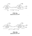
- FIG. 3 a and FIG. 3 b are sectional views of substrates for LCDs illustrating the variation in the aperture ratio depending on the increase in the line width of the metal line. Specifically, FIG. 3 a shows a status prior to increasing the line width of the metal line, and FIG. 3 b shows a status after the line width of the metal line increases.
- the metal line for the gate line and the data line are generally made of an opaque metal.
- the increase in the line width allows the light transmission area of a substrate 320 to be decreased from L1 to L2.
- the decrease in the light transmission area causes more of the light irradiated from a backlight to be lost while light is transmitted from the substrate resulting in the aperture ratio of the pixel being lowered.
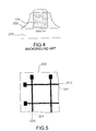
- FIG. 4 is a schematic view for illustrating that a crack is generated in the inorganic insulating film formed on the metal line.
- the background art method for forming the metal line has prevented process failures by decreasing the aperture ratio of the pixel so as to solve the signal delay problem.
- a substrate for a liquid crystal display includes: a line-shaped fine groove formed on the substrate; and a metal line at least formed within the fine groove.
- a substrate for a liquid crystal display includes: a plurality of first line-shaped fine grooves formed parallel to one another in a length direction on the substrate; a plurality of second line-shaped fine grooves formed parallel to one another in a width direction on the substrate; a first metal line at least formed within the first line-shaped fine grooves; and a second metal line at least formed within the second line-shaped fine grooves.
- a liquid crystal display in another aspect of the present invention, there is provided a liquid crystal display.
- the liquid crystal display includes: a TFT array substrate including thin film transistors, pixel electrodes, a line for supplying current to the thin film transistors, and a fine groove formed on the TFT array substrate and in which the line is received to reduce a height difference between the line and the surface of the TFT array substrate; a color filter substrate facing the TFT array substrate, and on which a color filter and a common electrode are formed; and a liquid crystal layer interposed between the TFT array substrate and the color filter substrate.
- the sectional area of the metal line can be increased and the resistance can be decreased, thereby achieving an objective of easily realizing a large-sized LCD.
- FIG. 1 is a plan view schematically showing a configuration of metal lines formed on a substrate for an LCD
- FIG. 2 is a perspective view of a metal line to depict the resistance characteristic of the metal line
- FIG. 3 a and FIG. 3 b are sectional views of substrates for LCDs illustrating the variation in the aperture ratio depending on the increase in the line width of the metal line;
- FIG. 4 is a schematic view for illustrating that a crack is generated in the inorganic insulating film formed on the metal line;
- FIG. 5 is a schematic view of metal lines formed on a substrate for a liquid crystal display according to an embodiment of the present invention.
- FIG. 6 is a schematic sectional view of the first metal line shown in FIG. 5;
- FIG. 7 is a schematic sectional view of the second metal line shown in FIG. 5.
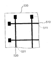
- FIG. 5 is a schematic view of metal lines formed on a substrate for a liquid crystal display according to an embodiment of the present invention.
- a substrate 530 for a liquid crystal display includes a plurality of first fine grooves 511 formed parallel to each other in a length direction on the substrate, and a plurality of second fine grooves 521 formed parallel to each other in a width direction perpendicular to the length direction on the substrate.
- a first metal line 510 including a gate line is formed at least within the first fine groove and a second metal line 520 including a data line is formed at least within the second fine groove 521 .
- Width and thickness of the first and second fine grooves 511 and 521 can be concretely determined by the line width and thickness of the first and second metal lines 510 and 520 formed on the first and second fine grooves 511 and 521 .
- the first and second metal lines 510 and 520 have a line width ranging from 7 ⁇ m to 20 ⁇ m and a thickness ranging from 1,000 ⁇ to 4,000 ⁇ .
- the first and second fine grooves 511 and 521 are also formed to have a line width ranging from 7 ⁇ m to 20 ⁇ m and a thickness ranging from 1,000 ⁇ to 4,000 ⁇ .
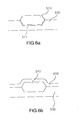
- a manufacturing process of the substrate for a liquid crystal display is described with reference to FIG. 6.
- FIG. 6 is a schematic sectional view of the first metal line shown in FIG. 5.
- a substrate 530 for forming TFTs and pixel electrodes is prepared.
- the substrate 530 is made of glass or plastic.
- a first fine groove 511 for the formation of a first metal line 510 including a gate line is formed in a length direction on the substrate 530 .
- the first fine groove 511 can be formed by an etch process. If the substrate 530 is made of plastic, the first fine groove 511 can be formed by a molding process using a die.
- a first metal line 511 is formed on the first fine groove 511 .
- a conductive material for instance, aluminum or an aluminum alloy is deposited on the substrate 530 , a photoresist film is coated on the conductive material, the photoresist film is patterned by a photolithography process, the underlying conductive material is selectively removed by an etch process with the patterned photoresist film as a mask, and the patterned photoresist film is then removed. The remaining conductive material pattern forms the first metal line 510 .
- the substrate formed as above does not cause a height difference problem between the uppermost surface of the first metal line 510 and the upper surface of the substrate 530 although it uses a thicker metal line than the metal line of the background art. Also, it is possible to further decrease the height difference by making the first fine groove 511 deeper. In other words, the height difference between the first metal line 510 and the substrate 530 decreases by the thickness of the substrate 530 .
- the metal line 510 decreases in line width but increases in thickness, it has an area that is equal to or greater than the area of the metal line in the background art. This means that resistance per unit length of the metal line decreases compared with the resistance of the background art.
- the metal line according to the present invention achieves a low resistance characteristic and accordingly the signal delay and the signal distortion phenomenon due to the voltage drop in the metal line decrease remarkably.
- FIG. 7 is a schematic sectional view of the second metal line shown in FIG. 5.
- a substrate for a liquid crystal display includes a second fine groove 521 formed in a width direction on the substrate, an inorganic insulating film 710 formed on a predetermined portion of the substrate including the second fine groove 521 , and a second metal line 520 formed on the inorganic insulating film 710 .
- a passivation layer 720 is further formed on the second metal line 520 and the inorganic insulating film 710 as shown in FIG. 7 b.
- the second metal line 520 is formed on the inorganic insulating film 710 as shown in FIG. 7 a.
- the inorganic insulating film 710 is provided to insulate the first metal line 510 (FIG. 5) and the second metal line 520 formed crosswise with the first metal line 510 .
- the inorganic insulating film 710 is insertedly formed on a contact surface between the first metal line 510 and the second metal line 520 at the crossing portion of the first metal line 510 and the second metal line 520 , but is formed between the second fine groove 521 and the second metal line 520 as shown in FIGS. 7 a and 7 b at a region other than the crossing portion.
- the inorganic insulating film 710 is formed in a recessed shape like the shape of the second fine groove 521 , although the second metal line 520 having a thickness greater than that of the background art is formed, the height difference decreases remarkably compared with the height difference in the background art. As a result, although an upper film such as the passivation layer 720 is formed, the possibility of crack occurrence decreases. Also, as shown in FIGS. 7 a and 7 b , since the side portions of the second metal line 520 are formed with a slope, the possibility in crack occurrence decreases remarkably.
- the forming processes of the second metal line 520 , the inorganic insulating film 710 and the passivation layer 720 can be formed by the same method as that of the first metal line 510 .
- first and second metal lines 510 and 520 have a thickness greater than a thickness of the lines in the background art, they have a height difference less than a height difference in the background art, due to the existence of the fine grooves.
- the quality of the upper films formed on the metal lines 510 and 520 i.e., the inorganic insulating film 610 and the passivation layer 720 is enhanced and the reliability in the manufacturing process is also improved.
- the aperture ratio of the pixels and the luminance are enhanced, so that a high resolution can be obtained.
Abstract
Description
- This nonprovisional application claims priority under 35 U.S.C. § 119(a) on patent application Ser. No. 20939/2002 filed in Korea on Apr. 17, 2002, which is herein incorporated by reference.
- 1. Field of the Invention
- The present invention relates to a substrate for a liquid crystal display, and more particularly, to a substrate for a liquid crystal display in which metal lines including a gate line and a data line are formed to be suitable for realizing a high resolution in a large-sized screen.
- 2. Discussion of the Background Art
- Generally, a liquid crystal display (LCD) includes a TFT (thin film transistor) array substrate on which thin film transistors (TFTs) and pixel electrodes are arranged and a color filter substrate facing the TFT array substrate on which color filters and a common electrode are formed, and a liquid crystal injected into a space between the TFT array substrate and the color filter substrate. These LCDs display images by using an optical switching property of the liquid crystal interposed between the two substrates. In recent times, LCDs are increasing in popularity as a next generation display device to replace the cathode ray tube (CRT) because of their light weight and slim characteristics.
- FIG. 1 is a plan view schematically showing a configuration of metal lines formed on a substrate for an LCD.
- As shown in FIG. 1, a plurality of metal lines are formed on a substrate for an LCD. For instance, the metal lines include a plurality of
gate lines 110 a to 110 n (110) formed in a length direction and a plurality ofdata lines 120 a to 120 n (120) formed in a width direction and perpendicularly crossed with the gate lines. A plurality ofgate line pads 111 a to 111 n (111) into which gate driving signals for respective pixels are inputted, are formed at one end of thegate lines 110. A plurality of data line pads 121 a to 121 n (121) into which data driving signals for respective pixels are inputted are formed at one end of thedata lines 120. - Here,
unit pixel 130 is defined as a region in which a pair of gate lines are crossed with a pair of data lines. - In detail, the
data lines 110 and thegate lines 120 are made of a conductive material and applies a driving current to the TFT element corresponding to thepixel 130. Thedata lines 110 and thegate lines 120 are formed by a method including the steps of depositing a metal film and a photoresist film on a substrate on which TFTs are arranged, and selectively removing the photoresist film and the metal film through a photolithography process. - As time progresses, the metal line including these gate lines and data lines is becoming increasingly lengthened according to a trend of increasing the size of LCDs.
- FIG. 2 is a perspective view of a metal line to depict the resistance characteristic of the metal line.
- When the length of the metal line is l, the sectional area is A, and the conductivity is 6, a total resistance of the metal line R equals to l/6A. Accordingly, if the flowing current is I, a voltage drop ΔV in the metal line is expressed by the following equation: ΔV=iR=il/6A. This relation means that when the sectional area A (including elements of the thickness and the line width) of the
gate line 110 and thedata line 120 is constant, the voltage drop ΔV depends on the respective lengths of thegate line 110 and thedata line 120. - As a result, although an equal driving voltage is applied to the
gate line pad 111 a and the data line pad 121 a from the drive IC (not shown) of the LCD, the voltages applied to thegate line 110 or thedata line 120 varies at a specific location depending on the resistance. For example, according to the lengths of thegate lines 110 and thedata lines 120, a lower voltage is applied to a pixel (Pn of FIG. 1) further away from thepads 111 a, 121 a than a pixel (Pa of FIG. 1) placed nearer to thepads 111 a, 121 a. Accordingly, the pixel (Pn of FIG. 1) needs a longer charging time than the pixel (Pa of FIG. 1) when the pixels (Pn and Pa) are charged up to a specific electric charge. In other words, if the resistance increases, the current flowing through under the same voltage decreases, so that the charging time is lengthened. - The extended charging time causes a signal delay phenomenon in which the frequency for driving the LCD panel is lowered.
- In order to solve this problem, it is necessary to decrease an overall resistance of the metal line by decreasing the length of the metal line, or increasing the sectional area of the metal line.
- However, upon considering the trend in increasing a size of the LCDs, it is substantially difficult to shorten the length of the metal line.
- A background art method for increasing the sectional area of the metal line, includes increasing the line width or increasing the thickness of the metal line.
- However, if the line width of the metal line increases and the thickness decreases, little improvement in the height difference corresponding to the decrease in the thickness is obtained, but the lowering in the aperture ratio of the pixel due to the increase in the line width results. The lowering phenomenon in the aperture ratio is described with reference to FIG. 3.
- FIG. 3 a and FIG. 3b are sectional views of substrates for LCDs illustrating the variation in the aperture ratio depending on the increase in the line width of the metal line. Specifically, FIG. 3a shows a status prior to increasing the line width of the metal line, and FIG. 3b shows a status after the line width of the metal line increases.
- The metal line for the gate line and the data line are generally made of an opaque metal. To this end, the increase in the line width allows the light transmission area of a
substrate 320 to be decreased from L1 to L2. The decrease in the light transmission area causes more of the light irradiated from a backlight to be lost while light is transmitted from the substrate resulting in the aperture ratio of the pixel being lowered. - The occurrence of the aforementioned phenomenon is not restricted only to the transmission type LCD substrate but is applied to the reflection type LCD substrate likewise.
- Of course, the problem of lowering in the aperture ratio can be resolved by increasing the thickness of the metal line instead of increasing the line width of the metal line.
- FIG. 4 is a schematic view for illustrating that a crack is generated in the inorganic insulating film formed on the metal line.
- As shown in FIG. 4, when the thickness of the metal line is increased, a serious height difference is generated between the metal line portion and the non-metal line portion. So, if the inorganic
insulating film 330 is further deposited on themetal line 120, a problem occurs in that a crack is generated in the inorganicinsulating film 330, so that many defective devices are mass-produced. Hence, the thickness of the metal line cannot be increased above a certain limit. - Because of the above problems, the background art method for forming the metal line has prevented process failures by decreasing the aperture ratio of the pixel so as to solve the signal delay problem.
- However, in the manufacturing process of a large-sized, high brightness and high resolution LCD sought after at the present time, there is a problem in applying the aforementioned methods due to a limitation on the application. Especially, in order to realize a large-sized LCD, it is essentially required to decrease the resistance of the metal line.
- To achieve these objects and other advantages and in accordance with the purpose of the invention, as embodied and broadly described herein, there is provided a substrate for a liquid crystal display. The substrate includes: a line-shaped fine groove formed on the substrate; and a metal line at least formed within the fine groove.
- In an aspect of the present invention, there is provided a substrate for a liquid crystal display. The substrate includes: a plurality of first line-shaped fine grooves formed parallel to one another in a length direction on the substrate; a plurality of second line-shaped fine grooves formed parallel to one another in a width direction on the substrate; a first metal line at least formed within the first line-shaped fine grooves; and a second metal line at least formed within the second line-shaped fine grooves.
- In another aspect of the present invention, there is provided a liquid crystal display. The liquid crystal display includes: a TFT array substrate including thin film transistors, pixel electrodes, a line for supplying current to the thin film transistors, and a fine groove formed on the TFT array substrate and in which the line is received to reduce a height difference between the line and the surface of the TFT array substrate; a color filter substrate facing the TFT array substrate, and on which a color filter and a common electrode are formed; and a liquid crystal layer interposed between the TFT array substrate and the color filter substrate.
- According to the above liquid crystal display, it is possible to decrease the resistance of the metal line formed on the substrate.
- In addition, the sectional area of the metal line can be increased and the resistance can be decreased, thereby achieving an objective of easily realizing a large-sized LCD.
- It is to be understood that both the foregoing general description and the following detailed description of the present invention are exemplary and explanatory and are intended to provide further explanation of the present invention as claimed.
- The accompanying drawings, which are included to provide a further understanding of the present invention and are incorporated in and constitute a part of this application, illustrate embodiment(s) of the present invention and together with the description serve to explain principles of the present invention. In the drawings:
- FIG. 1 is a plan view schematically showing a configuration of metal lines formed on a substrate for an LCD;
- FIG. 2 is a perspective view of a metal line to depict the resistance characteristic of the metal line;
- FIG. 3 a and FIG. 3b are sectional views of substrates for LCDs illustrating the variation in the aperture ratio depending on the increase in the line width of the metal line;
- FIG. 4 is a schematic view for illustrating that a crack is generated in the inorganic insulating film formed on the metal line;
- FIG. 5 is a schematic view of metal lines formed on a substrate for a liquid crystal display according to an embodiment of the present invention;
- FIG. 6 is a schematic sectional view of the first metal line shown in FIG. 5; and
- FIG. 7 is a schematic sectional view of the second metal line shown in FIG. 5.
- Reference will now be made in detail to a preferred embodiment of the present invention with reference to the attached drawings.
- FIG. 5 is a schematic view of metal lines formed on a substrate for a liquid crystal display according to an embodiment of the present invention.
- As shown in FIG. 5, a
substrate 530 for a liquid crystal display according to the present invention includes a plurality of firstfine grooves 511 formed parallel to each other in a length direction on the substrate, and a plurality of secondfine grooves 521 formed parallel to each other in a width direction perpendicular to the length direction on the substrate. Afirst metal line 510 including a gate line is formed at least within the first fine groove and asecond metal line 520 including a data line is formed at least within the secondfine groove 521. - Width and thickness of the first and second
fine grooves second metal lines fine grooves second metal lines fine grooves - A manufacturing process of the substrate for a liquid crystal display is described with reference to FIG. 6.
- FIG. 6 is a schematic sectional view of the first metal line shown in FIG. 5.
- First, referring to FIG. 6 a, a
substrate 530 for forming TFTs and pixel electrodes is prepared. Thesubstrate 530 is made of glass or plastic. A firstfine groove 511 for the formation of afirst metal line 510 including a gate line is formed in a length direction on thesubstrate 530. - In the meanwhile, if the
substrate 530 is made of glass, the firstfine groove 511 can be formed by an etch process. If thesubstrate 530 is made of plastic, the firstfine groove 511 can be formed by a molding process using a die. - If the first
fine groove 511 is formed on thesubstrate 530 by the etch process or the molding process, afirst metal line 511 is formed on the firstfine groove 511. In more detail, a conductive material, for instance, aluminum or an aluminum alloy is deposited on thesubstrate 530, a photoresist film is coated on the conductive material, the photoresist film is patterned by a photolithography process, the underlying conductive material is selectively removed by an etch process with the patterned photoresist film as a mask, and the patterned photoresist film is then removed. The remaining conductive material pattern forms thefirst metal line 510. - The substrate formed as above does not cause a height difference problem between the uppermost surface of the
first metal line 510 and the upper surface of thesubstrate 530 although it uses a thicker metal line than the metal line of the background art. Also, it is possible to further decrease the height difference by making the firstfine groove 511 deeper. In other words, the height difference between thefirst metal line 510 and thesubstrate 530 decreases by the thickness of thesubstrate 530. - Thus, as the height difference of the
metal line 510 decreases, although an upper film such as an inorganicinsulating film 610 is formed on thefirst metal line 510 as shown in FIG. 6b, the possibility of a crack occurring in the inorganicinsulating film 610 decreases remarkably, such that yield in the manufacturing process of the LCDS is enhanced. In addition, as shown in FIG. 6b, since the sidewall of themetal line 510 is formed with a slope, the possibility of a crack occurring further decreases. - Also, since the
metal line 510 decreases in line width but increases in thickness, it has an area that is equal to or greater than the area of the metal line in the background art. This means that resistance per unit length of the metal line decreases compared with the resistance of the background art. - In other words, the metal line according to the present invention achieves a low resistance characteristic and accordingly the signal delay and the signal distortion phenomenon due to the voltage drop in the metal line decrease remarkably.
- FIG. 7 is a schematic sectional view of the second metal line shown in FIG. 5.
- Referring to FIG. 7 a, a substrate for a liquid crystal display includes a second
fine groove 521 formed in a width direction on the substrate, an inorganicinsulating film 710 formed on a predetermined portion of the substrate including the secondfine groove 521, and asecond metal line 520 formed on the inorganicinsulating film 710. Apassivation layer 720 is further formed on thesecond metal line 520 and the inorganicinsulating film 710 as shown in FIG. 7b. - Particularly, the
second metal line 520 is formed on the inorganicinsulating film 710 as shown in FIG. 7a. - Here, the inorganic
insulating film 710 is provided to insulate the first metal line 510 (FIG. 5) and thesecond metal line 520 formed crosswise with thefirst metal line 510. In more detail, the inorganicinsulating film 710 is insertedly formed on a contact surface between thefirst metal line 510 and thesecond metal line 520 at the crossing portion of thefirst metal line 510 and thesecond metal line 520, but is formed between the secondfine groove 521 and thesecond metal line 520 as shown in FIGS. 7a and 7 b at a region other than the crossing portion. - Since the inorganic
insulating film 710 is formed in a recessed shape like the shape of the secondfine groove 521, although thesecond metal line 520 having a thickness greater than that of the background art is formed, the height difference decreases remarkably compared with the height difference in the background art. As a result, although an upper film such as thepassivation layer 720 is formed, the possibility of crack occurrence decreases. Also, as shown in FIGS. 7a and 7 b, since the side portions of thesecond metal line 520 are formed with a slope, the possibility in crack occurrence decreases remarkably. - In the meanwhile, the forming processes of the
second metal line 520, the inorganicinsulating film 710 and thepassivation layer 720 can be formed by the same method as that of thefirst metal line 510. - Thus, although the first and
second metal lines metal lines insulating film 610 and thepassivation layer 720 is enhanced and the reliability in the manufacturing process is also improved. - In addition, the aperture ratio of the pixels and the luminance are enhanced, so that a high resolution can be obtained.
- Further, it becomes possible to form the metal lines of the low resistance characteristic which is required in manufacturing a large-sized LCD without lowering of the aperture ratio or increase in the height difference.
- In particular, in case the substrate of the present invention is used, a high quality large-sized LCD can be produced and a high resolution even in a small-sized LCD can be obtained.
- The foregoing embodiment is merely exemplary and is not to be construed as limiting the present invention. The present teachings can be readily applied to other types of apparatuses. The description of the present invention is intended to be illustrative, and not to limit the scope of the claims. Many alternatives, modifications, and variations will be apparent to those skilled in the art.
Claims (19)
Priority Applications (1)
| Application Number | Priority Date | Filing Date | Title |
|---|---|---|---|
| US12/686,206 US7826021B2 (en) | 2002-04-17 | 2010-01-12 | Substrate for liquid crystal display |
Applications Claiming Priority (3)
| Application Number | Priority Date | Filing Date | Title |
|---|---|---|---|
| KR1020020020939A KR100860468B1 (en) | 2002-04-17 | 2002-04-17 | Substrate for Liquid Crystal Device |
| KR20939/2002 | 2002-04-17 | ||
| KR10-2002-0020939 | 2002-04-17 |
Related Child Applications (1)
| Application Number | Title | Priority Date | Filing Date |
|---|---|---|---|
| US12/686,206 Division US7826021B2 (en) | 2002-04-17 | 2010-01-12 | Substrate for liquid crystal display |
Publications (2)
| Publication Number | Publication Date |
|---|---|
| US20030197828A1 true US20030197828A1 (en) | 2003-10-23 |
| US7671953B2 US7671953B2 (en) | 2010-03-02 |
Family
ID=29208718
Family Applications (2)
| Application Number | Title | Priority Date | Filing Date |
|---|---|---|---|
| US10/329,470 Expired - Fee Related US7671953B2 (en) | 2002-04-17 | 2002-12-27 | Substrate for liquid crystal display |
| US12/686,206 Expired - Fee Related US7826021B2 (en) | 2002-04-17 | 2010-01-12 | Substrate for liquid crystal display |
Family Applications After (1)
| Application Number | Title | Priority Date | Filing Date |
|---|---|---|---|
| US12/686,206 Expired - Fee Related US7826021B2 (en) | 2002-04-17 | 2010-01-12 | Substrate for liquid crystal display |
Country Status (2)
| Country | Link |
|---|---|
| US (2) | US7671953B2 (en) |
| KR (1) | KR100860468B1 (en) |
Cited By (6)
| Publication number | Priority date | Publication date | Assignee | Title |
|---|---|---|---|---|
| US20070165147A1 (en) * | 2006-01-16 | 2007-07-19 | Seiko Epson Corporation | Electrooptical device, electronic apparatus, and projector |
| US20110001916A1 (en) * | 2005-12-29 | 2011-01-06 | Au Optronics Corporation | Liquid crystal display device |
| US20170372988A1 (en) * | 2016-06-23 | 2017-12-28 | Nxp B.V. | Wafer level chip scale semiconductor package |
| CN111240067A (en) * | 2020-02-28 | 2020-06-05 | 京东方科技集团股份有限公司 | Display panel, manufacturing method thereof and display device |
| WO2020206714A1 (en) * | 2019-04-09 | 2020-10-15 | 深圳市华星光电技术有限公司 | Circuit structure of display panel and manufacturing method therefor, and display device |
| CN114815426A (en) * | 2022-05-10 | 2022-07-29 | 广州华星光电半导体显示技术有限公司 | Array substrate and display panel |
Families Citing this family (5)
| Publication number | Priority date | Publication date | Assignee | Title |
|---|---|---|---|---|
| KR101116820B1 (en) * | 2004-11-23 | 2012-02-28 | 엘지디스플레이 주식회사 | Thin film transistor array substrate and manufacturing method of the same |
| KR200453958Y1 (en) * | 2011-01-13 | 2011-06-09 | 주식회사 한산에이엠에스텍크 | Circuit connection device and power meter using the same |
| TWI538140B (en) | 2011-12-16 | 2016-06-11 | 元太科技工業股份有限公司 | Three-dimension circuit structure and semiconductor device |
| CN104536207A (en) * | 2014-12-31 | 2015-04-22 | 京东方科技集团股份有限公司 | Display substrate and display device |
| CN106019659B (en) * | 2016-07-29 | 2019-12-06 | 京东方科技集团股份有限公司 | substrate and repairing method and manufacturing method thereof |
Citations (9)
| Publication number | Priority date | Publication date | Assignee | Title |
|---|---|---|---|---|
| US4913531A (en) * | 1988-09-07 | 1990-04-03 | Hughes Aircraft Company | Liquid crystal light valve with grooved microgrid and method of forming the same |
| US5214521A (en) * | 1991-10-26 | 1993-05-25 | Samsung Electron Devices Co., Ltd. | Plasma addressed liquid crystal display with grooves in middle plate |
| US5398127A (en) * | 1992-03-03 | 1995-03-14 | Matsushita Electric Industrial Co., Ltd. | Active matrix twisted nematic liquid crystal display with rubbing direction 1-44 degrees to the electrodes |
| US5892558A (en) * | 1997-06-26 | 1999-04-06 | Gl Displays, Inc. | Wire electrode structure based on 2 or 3 terminal device employed in a liquid crystal display |
| US6317175B1 (en) * | 1990-12-31 | 2001-11-13 | Kopin Corporation | Single crystal silicon arrayed devices with optical shield between transistor and substrate |
| US6610997B2 (en) * | 2000-03-17 | 2003-08-26 | Seiko Epson Corporation | Electro-optical device |
| US6628367B2 (en) * | 2000-07-28 | 2003-09-30 | Seiko Epson Corporation | Method for manufacturing electrooptical device, and electrooptical device |
| US6683592B1 (en) * | 1999-08-20 | 2004-01-27 | Seiko Epson Corporation | Electro-optical device |
| US6762809B1 (en) * | 1999-09-30 | 2004-07-13 | Seiko Epson Corporation | Electro-optical device and method for manufacturing the same |
Family Cites Families (7)
| Publication number | Priority date | Publication date | Assignee | Title |
|---|---|---|---|---|
| JPH03166525A (en) * | 1989-11-24 | 1991-07-18 | Toppan Printing Co Ltd | Production of active matrix substrate for liquid crystal display |
| JPH04170519A (en) * | 1990-11-01 | 1992-06-18 | Matsushita Electric Ind Co Ltd | Wiring for plane display and forming method thereof and nonlinear resistance element for liquid crystal display |
| US5317432A (en) * | 1991-09-04 | 1994-05-31 | Sony Corporation | Liquid crystal display device with a capacitor and a thin film transistor in a trench for each pixel |
| JP3230294B2 (en) * | 1992-08-31 | 2001-11-19 | ソニー株式会社 | Display device |
| JPH06273780A (en) * | 1993-03-18 | 1994-09-30 | Canon Inc | Production of liquid crystal device and liquid crystal device formed by using the same |
| JPH09274195A (en) * | 1996-04-04 | 1997-10-21 | Matsushita Electric Ind Co Ltd | Liquid crystal display device |
| KR100713878B1 (en) * | 2000-06-30 | 2007-05-07 | 비오이 하이디스 테크놀로지 주식회사 | Method for menufactuering flat panel display |
-
2002
- 2002-04-17 KR KR1020020020939A patent/KR100860468B1/en active IP Right Grant
- 2002-12-27 US US10/329,470 patent/US7671953B2/en not_active Expired - Fee Related
-
2010
- 2010-01-12 US US12/686,206 patent/US7826021B2/en not_active Expired - Fee Related
Patent Citations (9)
| Publication number | Priority date | Publication date | Assignee | Title |
|---|---|---|---|---|
| US4913531A (en) * | 1988-09-07 | 1990-04-03 | Hughes Aircraft Company | Liquid crystal light valve with grooved microgrid and method of forming the same |
| US6317175B1 (en) * | 1990-12-31 | 2001-11-13 | Kopin Corporation | Single crystal silicon arrayed devices with optical shield between transistor and substrate |
| US5214521A (en) * | 1991-10-26 | 1993-05-25 | Samsung Electron Devices Co., Ltd. | Plasma addressed liquid crystal display with grooves in middle plate |
| US5398127A (en) * | 1992-03-03 | 1995-03-14 | Matsushita Electric Industrial Co., Ltd. | Active matrix twisted nematic liquid crystal display with rubbing direction 1-44 degrees to the electrodes |
| US5892558A (en) * | 1997-06-26 | 1999-04-06 | Gl Displays, Inc. | Wire electrode structure based on 2 or 3 terminal device employed in a liquid crystal display |
| US6683592B1 (en) * | 1999-08-20 | 2004-01-27 | Seiko Epson Corporation | Electro-optical device |
| US6762809B1 (en) * | 1999-09-30 | 2004-07-13 | Seiko Epson Corporation | Electro-optical device and method for manufacturing the same |
| US6610997B2 (en) * | 2000-03-17 | 2003-08-26 | Seiko Epson Corporation | Electro-optical device |
| US6628367B2 (en) * | 2000-07-28 | 2003-09-30 | Seiko Epson Corporation | Method for manufacturing electrooptical device, and electrooptical device |
Cited By (9)
| Publication number | Priority date | Publication date | Assignee | Title |
|---|---|---|---|---|
| US20110001916A1 (en) * | 2005-12-29 | 2011-01-06 | Au Optronics Corporation | Liquid crystal display device |
| US8013965B2 (en) * | 2005-12-29 | 2011-09-06 | Au Optronics Corporation | Liquid crystal display device comprising a passivation layer which forms two inclined planes on opposing sides of grooves formed on a top surface of the lower substrate |
| US20070165147A1 (en) * | 2006-01-16 | 2007-07-19 | Seiko Epson Corporation | Electrooptical device, electronic apparatus, and projector |
| US7924356B2 (en) | 2006-01-16 | 2011-04-12 | Seiko Epson Corporation | Electrooptical device, electronic apparatus, and projector |
| US20170372988A1 (en) * | 2016-06-23 | 2017-12-28 | Nxp B.V. | Wafer level chip scale semiconductor package |
| US10109564B2 (en) * | 2016-06-23 | 2018-10-23 | Nxp B.V. | Wafer level chip scale semiconductor package |
| WO2020206714A1 (en) * | 2019-04-09 | 2020-10-15 | 深圳市华星光电技术有限公司 | Circuit structure of display panel and manufacturing method therefor, and display device |
| CN111240067A (en) * | 2020-02-28 | 2020-06-05 | 京东方科技集团股份有限公司 | Display panel, manufacturing method thereof and display device |
| CN114815426A (en) * | 2022-05-10 | 2022-07-29 | 广州华星光电半导体显示技术有限公司 | Array substrate and display panel |
Also Published As
| Publication number | Publication date |
|---|---|
| US7671953B2 (en) | 2010-03-02 |
| US7826021B2 (en) | 2010-11-02 |
| KR20030082285A (en) | 2003-10-22 |
| US20100112740A1 (en) | 2010-05-06 |
| KR100860468B1 (en) | 2008-09-25 |
Similar Documents
| Publication | Publication Date | Title |
|---|---|---|
| US7826021B2 (en) | Substrate for liquid crystal display | |
| US7075595B2 (en) | Liquid crystal display device array substrate and method of manufacturing the same | |
| KR100271037B1 (en) | Structure and fabrication method of lcd | |
| US8362491B2 (en) | Liquid crystal display device and method for fabricating the same | |
| KR100469342B1 (en) | Liquid Crystal Display Device | |
| US7671931B2 (en) | Liquid crystal display device and method of fabricating the same | |
| US6801289B2 (en) | Liquid crystal display device | |
| US7365825B2 (en) | Liquid crystal display device including repair pattern and method for fabricating the same | |
| KR20010015187A (en) | Thin film transistor array and its manufacturing method | |
| US20020085149A1 (en) | Liquid crystal display device and method for manufacturing the same | |
| US6657226B1 (en) | Thin-film transistor array and method for manufacturing same | |
| US20080100765A1 (en) | Ffs mode lcd | |
| US6900871B1 (en) | Thin film transistor substrate of liquid crystal display and method of manufacture | |
| US5731854A (en) | Method of effectively dispersing static electricity in LCD production by placing a short line in the end region of one substrate which extends beyond the other substrate | |
| US6330042B1 (en) | Liquid crystal display and the method of manufacturing the same | |
| US8059221B2 (en) | Liquid crystal display and manufacturing method of the same | |
| KR100640089B1 (en) | Reflective-type liquid crystal display device and method for manufacturing the same | |
| KR20000039802A (en) | Method for manufacturing lower substrate of thin film transistor liquid crystal display device | |
| KR100771905B1 (en) | Structure and its fabrication method of thin film transistor liquid crystal display | |
| US6844901B2 (en) | Liquid crystal display device and method of manufacturing the same | |
| KR100640985B1 (en) | Liquid crystal display and method for fabricating the same | |
| KR100487434B1 (en) | Liquid Crystal Display Device and Method for Manufacturing the Same | |
| KR100514764B1 (en) | Liquid crystal display device and the method for manufaturing the same |
Legal Events
| Date | Code | Title | Description |
|---|---|---|---|
| AS | Assignment |
Owner name: LG. PHILIPS LCD CO., LTD., KOREA, REPUBLIC OF Free format text: ASSIGNMENT OF ASSIGNORS INTEREST;ASSIGNOR:HA, KYOUNG SU;REEL/FRAME:013793/0721 Effective date: 20021226 Owner name: LG. PHILIPS LCD CO., LTD.,KOREA, REPUBLIC OF Free format text: ASSIGNMENT OF ASSIGNORS INTEREST;ASSIGNOR:HA, KYOUNG SU;REEL/FRAME:013793/0721 Effective date: 20021226 |
|
| AS | Assignment |
Owner name: LG DISPLAY CO., LTD., KOREA, REPUBLIC OF Free format text: CHANGE OF NAME;ASSIGNOR:LG.PHILIPS LCD CO., LTD.;REEL/FRAME:020985/0675 Effective date: 20080304 Owner name: LG DISPLAY CO., LTD.,KOREA, REPUBLIC OF Free format text: CHANGE OF NAME;ASSIGNOR:LG.PHILIPS LCD CO., LTD.;REEL/FRAME:020985/0675 Effective date: 20080304 |
|
| FEPP | Fee payment procedure |
Free format text: PAYOR NUMBER ASSIGNED (ORIGINAL EVENT CODE: ASPN); ENTITY STATUS OF PATENT OWNER: LARGE ENTITY |
|
| STCF | Information on status: patent grant |
Free format text: PATENTED CASE |
|
| FPAY | Fee payment |
Year of fee payment: 4 |
|
| FPAY | Fee payment |
Year of fee payment: 8 |
|
| FEPP | Fee payment procedure |
Free format text: MAINTENANCE FEE REMINDER MAILED (ORIGINAL EVENT CODE: REM.); ENTITY STATUS OF PATENT OWNER: LARGE ENTITY |
|
| LAPS | Lapse for failure to pay maintenance fees |
Free format text: PATENT EXPIRED FOR FAILURE TO PAY MAINTENANCE FEES (ORIGINAL EVENT CODE: EXP.); ENTITY STATUS OF PATENT OWNER: LARGE ENTITY |
|
| STCH | Information on status: patent discontinuation |
Free format text: PATENT EXPIRED DUE TO NONPAYMENT OF MAINTENANCE FEES UNDER 37 CFR 1.362 |
|
| FP | Lapsed due to failure to pay maintenance fee |
Effective date: 20220302 |