US20030194840A1 - Method of manufacturing semiconductor device with reduced number of process steps for capacitor formation - Google Patents
Method of manufacturing semiconductor device with reduced number of process steps for capacitor formation Download PDFInfo
- Publication number
- US20030194840A1 US20030194840A1 US10/262,920 US26292002A US2003194840A1 US 20030194840 A1 US20030194840 A1 US 20030194840A1 US 26292002 A US26292002 A US 26292002A US 2003194840 A1 US2003194840 A1 US 2003194840A1
- Authority
- US
- United States
- Prior art keywords
- film
- forming
- electrode
- trench
- steps
- Prior art date
- Legal status (The legal status is an assumption and is not a legal conclusion. Google has not performed a legal analysis and makes no representation as to the accuracy of the status listed.)
- Granted
Links
- 238000000034 method Methods 0.000 title claims abstract description 120
- 239000003990 capacitor Substances 0.000 title claims abstract description 110
- 239000004065 semiconductor Substances 0.000 title claims abstract description 45
- 238000004519 manufacturing process Methods 0.000 title claims abstract description 34
- 230000015572 biosynthetic process Effects 0.000 title abstract description 17
- 229910021332 silicide Inorganic materials 0.000 claims abstract description 82
- FVBUAEGBCNSCDD-UHFFFAOYSA-N silicide(4-) Chemical compound [Si-4] FVBUAEGBCNSCDD-UHFFFAOYSA-N 0.000 claims abstract description 82
- 229910052751 metal Inorganic materials 0.000 claims abstract description 70
- 239000002184 metal Substances 0.000 claims abstract description 70
- 239000010410 layer Substances 0.000 claims description 96
- 238000009413 insulation Methods 0.000 claims description 57
- 238000005530 etching Methods 0.000 claims description 51
- 239000011229 interlayer Substances 0.000 claims description 45
- 238000002955 isolation Methods 0.000 claims description 35
- 239000000758 substrate Substances 0.000 claims description 22
- 239000012535 impurity Substances 0.000 claims description 19
- 239000000463 material Substances 0.000 claims description 5
- VYPSYNLAJGMNEJ-UHFFFAOYSA-N Silicium dioxide Chemical compound O=[Si]=O VYPSYNLAJGMNEJ-UHFFFAOYSA-N 0.000 description 53
- 229910052814 silicon oxide Inorganic materials 0.000 description 53
- 229910052581 Si3N4 Inorganic materials 0.000 description 36
- HQVNEWCFYHHQES-UHFFFAOYSA-N silicon nitride Chemical compound N12[Si]34N5[Si]62N3[Si]51N64 HQVNEWCFYHHQES-UHFFFAOYSA-N 0.000 description 36
- 229920002120 photoresistant polymer Polymers 0.000 description 34
- 238000001312 dry etching Methods 0.000 description 19
- 229910021420 polycrystalline silicon Inorganic materials 0.000 description 18
- 229920005591 polysilicon Polymers 0.000 description 18
- RYGMFSIKBFXOCR-UHFFFAOYSA-N Copper Chemical compound [Cu] RYGMFSIKBFXOCR-UHFFFAOYSA-N 0.000 description 16
- XUIMIQQOPSSXEZ-UHFFFAOYSA-N Silicon Chemical compound [Si] XUIMIQQOPSSXEZ-UHFFFAOYSA-N 0.000 description 14
- 229910052802 copper Inorganic materials 0.000 description 14
- 239000010949 copper Substances 0.000 description 14
- 229910052710 silicon Inorganic materials 0.000 description 14
- 239000010703 silicon Substances 0.000 description 14
- 239000011295 pitch Substances 0.000 description 12
- 238000005468 ion implantation Methods 0.000 description 7
- 229910017052 cobalt Inorganic materials 0.000 description 4
- 239000010941 cobalt Substances 0.000 description 4
- GUTLYIVDDKVIGB-UHFFFAOYSA-N cobalt atom Chemical compound [Co] GUTLYIVDDKVIGB-UHFFFAOYSA-N 0.000 description 4
- 238000010438 heat treatment Methods 0.000 description 4
- WFKWXMTUELFFGS-UHFFFAOYSA-N tungsten Chemical compound [W] WFKWXMTUELFFGS-UHFFFAOYSA-N 0.000 description 4
- 229910052721 tungsten Inorganic materials 0.000 description 4
- 239000010937 tungsten Substances 0.000 description 4
- 230000003647 oxidation Effects 0.000 description 3
- 238000007254 oxidation reaction Methods 0.000 description 3
- 230000002093 peripheral effect Effects 0.000 description 3
- 238000005498 polishing Methods 0.000 description 3
- PNEYBMLMFCGWSK-UHFFFAOYSA-N aluminium oxide Inorganic materials [O-2].[O-2].[O-2].[Al+3].[Al+3] PNEYBMLMFCGWSK-UHFFFAOYSA-N 0.000 description 2
- 229910052454 barium strontium titanate Inorganic materials 0.000 description 2
- 229910052593 corundum Inorganic materials 0.000 description 2
- 229910052451 lead zirconate titanate Inorganic materials 0.000 description 2
- PBCFLUZVCVVTBY-UHFFFAOYSA-N tantalum pentoxide Inorganic materials O=[Ta](=O)O[Ta](=O)=O PBCFLUZVCVVTBY-UHFFFAOYSA-N 0.000 description 2
- 229910001845 yogo sapphire Inorganic materials 0.000 description 2
- 230000015556 catabolic process Effects 0.000 description 1
- 238000006731 degradation reaction Methods 0.000 description 1
- 230000000694 effects Effects 0.000 description 1
- 239000012212 insulator Substances 0.000 description 1
- 238000012986 modification Methods 0.000 description 1
- 230000004048 modification Effects 0.000 description 1
- 238000000059 patterning Methods 0.000 description 1
- 239000000126 substance Substances 0.000 description 1
Images


Classifications
-
- H—ELECTRICITY
- H01—ELECTRIC ELEMENTS
- H01L—SEMICONDUCTOR DEVICES NOT COVERED BY CLASS H10
- H01L21/00—Processes or apparatus adapted for the manufacture or treatment of semiconductor or solid state devices or of parts thereof
- H01L21/02—Manufacture or treatment of semiconductor devices or of parts thereof
- H01L21/04—Manufacture or treatment of semiconductor devices or of parts thereof the devices having at least one potential-jump barrier or surface barrier, e.g. PN junction, depletion layer or carrier concentration layer
- H01L21/18—Manufacture or treatment of semiconductor devices or of parts thereof the devices having at least one potential-jump barrier or surface barrier, e.g. PN junction, depletion layer or carrier concentration layer the devices having semiconductor bodies comprising elements of Group IV of the Periodic System or AIIIBV compounds with or without impurities, e.g. doping materials
- H01L21/28—Manufacture of electrodes on semiconductor bodies using processes or apparatus not provided for in groups H01L21/20 - H01L21/268
- H01L21/283—Deposition of conductive or insulating materials for electrodes conducting electric current
- H01L21/285—Deposition of conductive or insulating materials for electrodes conducting electric current from a gas or vapour, e.g. condensation
- H01L21/28506—Deposition of conductive or insulating materials for electrodes conducting electric current from a gas or vapour, e.g. condensation of conductive layers
- H01L21/28512—Deposition of conductive or insulating materials for electrodes conducting electric current from a gas or vapour, e.g. condensation of conductive layers on semiconductor bodies comprising elements of Group IV of the Periodic System
- H01L21/28518—Deposition of conductive or insulating materials for electrodes conducting electric current from a gas or vapour, e.g. condensation of conductive layers on semiconductor bodies comprising elements of Group IV of the Periodic System the conductive layers comprising silicides
-
- H—ELECTRICITY
- H01—ELECTRIC ELEMENTS
- H01L—SEMICONDUCTOR DEVICES NOT COVERED BY CLASS H10
- H01L23/00—Details of semiconductor or other solid state devices
- H01L23/52—Arrangements for conducting electric current within the device in operation from one component to another, i.e. interconnections, e.g. wires, lead frames
- H01L23/522—Arrangements for conducting electric current within the device in operation from one component to another, i.e. interconnections, e.g. wires, lead frames including external interconnections consisting of a multilayer structure of conductive and insulating layers inseparably formed on the semiconductor body
- H01L23/5222—Capacitive arrangements or effects of, or between wiring layers
- H01L23/5223—Capacitor integral with wiring layers
-
- H—ELECTRICITY
- H01—ELECTRIC ELEMENTS
- H01L—SEMICONDUCTOR DEVICES NOT COVERED BY CLASS H10
- H01L28/00—Passive two-terminal components without a potential-jump or surface barrier for integrated circuits; Details thereof; Multistep manufacturing processes therefor
- H01L28/40—Capacitors
- H01L28/60—Electrodes
- H01L28/75—Electrodes comprising two or more layers, e.g. comprising a barrier layer and a metal layer
-
- H—ELECTRICITY
- H01—ELECTRIC ELEMENTS
- H01L—SEMICONDUCTOR DEVICES NOT COVERED BY CLASS H10
- H01L21/00—Processes or apparatus adapted for the manufacture or treatment of semiconductor or solid state devices or of parts thereof
- H01L21/70—Manufacture or treatment of devices consisting of a plurality of solid state components formed in or on a common substrate or of parts thereof; Manufacture of integrated circuit devices or of parts thereof
- H01L21/71—Manufacture of specific parts of devices defined in group H01L21/70
- H01L21/768—Applying interconnections to be used for carrying current between separate components within a device comprising conductors and dielectrics
- H01L21/76801—Applying interconnections to be used for carrying current between separate components within a device comprising conductors and dielectrics characterised by the formation and the after-treatment of the dielectrics, e.g. smoothing
- H01L21/76802—Applying interconnections to be used for carrying current between separate components within a device comprising conductors and dielectrics characterised by the formation and the after-treatment of the dielectrics, e.g. smoothing by forming openings in dielectrics
- H01L21/76807—Applying interconnections to be used for carrying current between separate components within a device comprising conductors and dielectrics characterised by the formation and the after-treatment of the dielectrics, e.g. smoothing by forming openings in dielectrics for dual damascene structures
-
- H—ELECTRICITY
- H01—ELECTRIC ELEMENTS
- H01L—SEMICONDUCTOR DEVICES NOT COVERED BY CLASS H10
- H01L29/00—Semiconductor devices adapted for rectifying, amplifying, oscillating or switching, or capacitors or resistors with at least one potential-jump barrier or surface barrier, e.g. PN junction depletion layer or carrier concentration layer; Details of semiconductor bodies or of electrodes thereof ; Multistep manufacturing processes therefor
- H01L29/66—Types of semiconductor device ; Multistep manufacturing processes therefor
- H01L29/66007—Multistep manufacturing processes
- H01L29/66075—Multistep manufacturing processes of devices having semiconductor bodies comprising group 14 or group 13/15 materials
- H01L29/66227—Multistep manufacturing processes of devices having semiconductor bodies comprising group 14 or group 13/15 materials the devices being controllable only by the electric current supplied or the electric potential applied, to an electrode which does not carry the current to be rectified, amplified or switched, e.g. three-terminal devices
- H01L29/66409—Unipolar field-effect transistors
- H01L29/66477—Unipolar field-effect transistors with an insulated gate, i.e. MISFET
- H01L29/665—Unipolar field-effect transistors with an insulated gate, i.e. MISFET using self aligned silicidation, i.e. salicide
-
- H—ELECTRICITY
- H01—ELECTRIC ELEMENTS
- H01L—SEMICONDUCTOR DEVICES NOT COVERED BY CLASS H10
- H01L2924/00—Indexing scheme for arrangements or methods for connecting or disconnecting semiconductor or solid-state bodies as covered by H01L24/00
- H01L2924/0001—Technical content checked by a classifier
- H01L2924/0002—Not covered by any one of groups H01L24/00, H01L24/00 and H01L2224/00
Definitions
- the present invention relates to a method of manufacturing a semiconductor device and a method of forming a capacitor.
- FIGS. 57 to 61 are cross sectional views showing a sequence of process steps in a first conventional semiconductor device manufacturing method.
- an element isolation insulating film 201 is partially formed in the upper surface of a silicon substrate 200 .
- a polysilicon film 202 serving as a lower electrode of a capacitor is partially formed on the element isolation insulating film 201 .
- an insulation film 203 serving as a capacitor dielectric film is formed on the element isolation insulating film 201 to cover the polysilicon film 202 .
- the insulation film 203 is, for example, an ON film formed by stacking silicon oxide film and silicon nitride film one above the other.
- a silicon oxide film 204 is formed by thermal oxidation on an upper surface portion of the silicon substrate 200 where the element isolation insulating film 201 is not formed.
- the polysilicon film is patterned to form a gate electrode 205 and a polysilicon film 206 serving as an upper electrode of the capacitor.
- the polysilicon film 206 is opposed to the polysilicon film 202 with the insulation film 203 sandwiched in between.
- source/drain regions 207 are formed in the upper surface of the silicon substrate 200 by ion implantation of impurities. At this time, impurities are also implanted into the gate electrode 205 and the polysilicon film 206 .
- FIGS. 62 to 67 are cross sectional views showing a sequence of process steps in a second conventional semiconductor device manufacturing method.
- a copper film 301 serving as a lower electrode of a capacitor is partially formed in the upper surface of an interlayer insulation film 300 .
- a capping film 302 of silicon nitride film is formed on the whole surface.
- the capping film is formed to prevent copper atoms contained in a copper wire from diffusing into the interlayer insulation film.
- a silicon oxide film 303 is formed on the capping film 302 .
- a photoresist 304 having a predetermined opening pattern is formed on the silicon oxide film 303 .
- the silicon oxide film 303 and the capping film 302 are etched to form a trench 305 .
- an insulation film 306 such as an ON film is formed on the whole surface.
- a copper film 307 is formed on the whole surface. Then, referring to FIG. 67, the copper film 307 and the insulation film 306 are polished by CMP (Chemical Mechanical Polishing) until the upper surface of the silicon oxide film 303 is exposed. This forms an insulation film 308 serving as a capacitor dielectric film and a copper film 309 serving as an upper electrode of the capacitor in the trench 305 .
- CMP Chemical Mechanical Polishing
- the impurities are introduced by ion implantation into the polysilicon film 206 serving as the upper electrode of the capacitor.
- the impurity concentration of the polysilicon film 206 in the bottom part is lower than that in the upper part. That is, the polysilicon film 206 has a low impurity concentration in a portion where it is in contact with the insulation film 203 serving as a capacitor dielectric film. This causes depletion of the polysilicon film 206 at the interface with the insulation film 203 , thereby causing a problem of capacitor performance degradation such as variations in capacitance due to changes in the applied voltage or temperature.
- An object of the present invention is to provide a method of manufacturing a semiconductor device and a method of forming a capacitor which allow the formation of a high-performance capacitor without increasing the number of process steps.
- the method of manufacturing a semiconductor device includes the following steps (a) to (g).
- the step (a) is to prepare a substrate.
- the step (b) is to partially form an element isolation insulating film in a main surface of the substrate.
- the step (c) is to form a first semiconductor element in a first element forming region defined by the element isolation insulating film, the first semiconductor element having first source/drain regions formed in the main surface.
- the step (d) is to form a first electrode of a capacitor.
- the step (e) is to form a silicide protection film of insulation film to cover the first electrode, but not to cover the first semiconductor element.
- the step (f) is to form a first silicide layer by silicidation of the first source/drain regions.
- the step (g) is to form a second electrode of the capacitor which is opposed to the first electrode with the silicide protection film sandwiched in between.
- the silicide protection film serves as a capacitor dielectric film.
- the number of process steps can be reduced when compared with that in the case where a capacitor dielectric film is formed aside from a silicide protection film.
- the method of manufacturing a semiconductor device includes the following steps (a) to (f).
- the step (a) is to prepare a substrate.
- the step (b) is to partially form an element isolation insulating film in a main surface of the substrate.
- the step (c) is to form a semiconductor element in a first element forming region defined by the element isolation insulating film, the semiconductor element having source/drain regions formed in the main surface.
- the step (d) is to form a first electrode of a capacitor.
- the step (e) is to form an etching stopper film of insulation film to cover the semiconductor element and the first electrode.
- the step (f) is to form a second electrode of the capacitor which is opposed to the first electrode with the etching stopper film sandwiched in between.
- the etching stopper film serves as a capacitor dielectric film.
- the number of process steps can be reduced when compared with that in the case where a capacitor dielectric film is formed aside from an etching stopper film.
- the method of manufacturing a semiconductor device includes the following steps (a) to (c).
- the step (a) is to form a first metal film serving as a first interconnection and a second metal film serving as a first electrode of a capacitor, within a first interconnection layer.
- the step (b) is to form a capping film to cover the first and second metal films.
- the step (c) is to form a third metal film serving as a second electrode of the capacitor within a second interconnection layer formed on the first interconnection layer, the third metal film being opposed to the second metal film with the capping film sandwiched in between.
- the capping film serves as a capacitor dielectric film.
- the number of process steps can be reduced when compared with that in the case where a capacitor dielectric film is formed aside from a capping film.
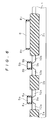
- FIGS. 1 to 13 are cross sectional views showing a sequence of process steps in a semiconductor device manufacturing method according to a first preferred embodiment of the present invention
- FIGS. 14 to 18 are cross sectional views showing a sequence of process steps in a semiconductor device manufacturing method according to a second preferred embodiment of the present invention.
- FIGS. 19 to 26 are cross sectional views showing a sequence of process steps in a semiconductor device manufacturing method according to a third preferred embodiment of the present invention.
- FIGS. 27 to 31 are cross sectional views showing a sequence of process steps in a semiconductor device manufacturing method according to a fourth preferred embodiment of the present invention.
- FIG. 32 is a perspective view showing a capacitor structure according to a fifth preferred embodiment of the present invention.
- FIG. 33 is a top view showing the capacitor structure according to the fifth preferred embodiment of the present invention.
- FIG. 34 is a cross sectional view of a section taken along line K-K of FIG. 33;
- FIGS. 35 to 38 are cross sectional views showing a sequence of process steps in a method of forming a capacitor according to the fifth preferred embodiment of the present invention.
- FIG. 39 is a cross sectional view showing a capacitor structure according to a sixth preferred embodiment of the present invention.
- FIGS. 40 to 43 are cross sectional views showing a sequence of process steps in a method of forming a capacitor according to the sixth preferred embodiment of the present invention.
- FIG. 44 is a cross sectional view showing a capacitor structure according to a seventh preferred embodiment of the present invention.
- FIG. 45 is a cross sectional view showing a capacitor structure according to an eighth preferred embodiment of the present invention.
- FIGS. 46 to 50 are cross sectional views showing a sequence of process steps in a semiconductor manufacturing method according to a ninth preferred embodiment of the present invention.
- FIGS. 51 to 56 are cross sectional views showing a sequence of process steps in a method of forming a capacitor according to a tenth preferred embodiment of the present invention.
- FIGS. 57 to 61 are cross sectional views showing a sequence of process steps in a first conventional semiconductor device manufacturing method.
- FIGS. 62 to 67 are cross sectional views showing a sequence of process steps in a second conventional semiconductor device manufacturing method.
- FIGS. 1 to 13 are cross sectional views showing a sequence of process steps in a semiconductor device manufacturing method according to a first preferred embodiment of the present invention.
- element isolation insulating films 2 a to 2 c of silicon oxide film are formed in the upper surface of a silicon substrate 1 .
- silicon oxide films 3 a and 3 b are formed by thermal oxidation on upper surface portions of the silicon substrate 1 where the element isolation insulating films 2 a to 2 c are not formed.
- the silicon oxide film 3 a is formed in an element forming region defined by the element isolation insulating films 2 a and 2 b.
- the silicon oxide film 3 b is formed in an element forming region defined by the element isolation insulating films 2 b and 2 c.
- a polysilicon film 4 is formed by CVD on the whole surface. Then, n- or p-type impurities are introduced by ion implantation into the polysilicon film 4 .
- the impurity concentration of the polysilicon film 4 in the upper part is higher than that in the bottom part.
- the upper surface of the polysilicon film 4 may be silicided, or a silicide film may be deposited on the upper surface of the polysilicon film 4 .
- the polysilicon film 4 is patterned by photolithographic and anisotropic dry etching techniques to form gate electrodes 5 a and 5 b and a lower electrode 6 of a capacitor.
- the gate electrodes 5 a and 5 b are partially formed on the silicon oxide films 3 a and 3 b, respectively.
- the lower electrode 6 is partially formed on the element isolation insulating film 2 c.
- impurities are introduced by ion implantation into the upper surface of the silicon substrate 1 to form a pair of LDD regions 7 a and a pair of LDD regions 7 b.
- the pair of LDD regions 7 a are opposed to each other with a channel forming region under the gate electrode 5 a sandwiched in between.
- the pair of LDD regions 7 b are opposed to each other with a channel forming region under the gate electrode 5 b sandwiched in between.
- a silicon oxide film is formed by CVD on the whole surface.
- the silicon oxide film is then etched by anisotropic dry etching until the upper surface of the silicon substrate 1 is exposed, whereby sidewalls 8 a to 8 c are formed.
- the sidewalls 8 a and 8 b are formed on the sides of the gate electrodes 5 a and 5 b, respectively.
- the sidewall 8 c is formed on the side of the lower electrode 6 .
- gate insulating films 9 a and 9 b are formed under the gate electrodes 5 a and 5 b, respectively.
- impurities are introduced by ion implantation into the upper surface of the silicon substrate 1 to form a pair of source/drain regions 10 a and a pair of source/drain regions 10 b.
- the pair of source/drain regions 10 a is opposed to each other with the channel forming region under the gate electrode 5 a sandwiched in between.
- the pair of source/drain regions 10 b are opposed to each other with the channel forming region under the gate electrode 5 b sandwiched in between.
- a MOSFET (hereinafter referred to as a “first MOSFET”) is formed in the element forming region defined by the element isolation insulating film 2 b and 2 c, and a MOSFET (hereinafter referred to as a “second MOSFET”) is formed in the element forming region defined by the element isolation insulating films 2 a and 2 b.
- a silicon oxide film is formed by CVD on the whole surface.
- the silicon oxide film is then patterned by photolithographic and anisotropic dry etching techniques to form silicide protection films 11 a and 11 c.
- the silicide protection film 11 a is formed to expose part of the upper surfaces of the source/drain regions 10 a and to cover the second MOSFET.
- the silicide protection film 11 c is formed to cover the lower electrode 6 .
- the first MOSFET is not covered with the silicide protection films 11 a and 11 c.
- heat treatment is performed after a metal film such as cobalt is formed on the whole surface.
- a metal film such as cobalt is formed on the whole surface.
- exposed upper surfaces portions of the source/drain regions 10 a which are not covered with the silicide protection film 11 a are silicided, forming silicide layers 12 a.
- the upper surfaces of the source/drain regions 10 b are silicided, forming silicide layers 12 b 2 .
- the upper surface of the gate electrode 5 b is also silicided, forming a silicide layer 12 b 1 .
- an unreacted metal film is removed.
- an etching stopper film 13 of silicon nitride film and an interlayer insulation film 14 of silicon oxide film are formed in this order on the whole surface by CVD.
- a photoresist 15 having a predetermined opening pattern is formed on the upper surface of the interlayer insulation film 14 by photolithographic techniques. Using the photoresist 15 as an etch mask, the interlayer insulation film 14 is removed by anisotropic dry etching until the upper surface of the etching stopper film 13 is exposed. This forms contact holes 16 a and 16 b above each of the silicide layers 12 a and 12 b 2 , respectively. Also, a trench 16 c is formed above the lower electrode 6 . The bottom surfaces of the contact holes 16 a, 16 b and the trench 16 c are defined by the upper surface of the etching stopper film 13 .
- the etching stopper film 13 is removed by anisotropic dry etching. Thereby, portions of the etching stopper film 13 which define the bottom surfaces of the contact holes 16 a and 16 b are removed and the upper surfaces of the silicide layers 12 a and 12 b 2 are exposed. Also, a portion of the etching stopper film 13 which defines the bottom surface of the trench 16 c is removed and the upper surface of the silicide protection film 11 c is exposed. As shown in FIG. 11, the bottom surfaces of the contact holes 16 a and 16 b are defined by the upper surfaces of the silicide layers 12 a and 12 b 2 , respectively. The bottom surface of the trench 16 c is defined by the upper surface of the silicide protection film 11 c.
- a metal film 17 such as tungsten is formed by CVD on the whole surface to such a film thickness as to completely fill in the contact holes 16 a and 16 b and the trench 16 c.
- the metal film 17 is removed by etch back or CMP techniques until the upper surface of the interlayer insulation film 14 is exposed. This forms plugs 18 a and 18 b to fill in the contact holes 16 a and 16 b, respectively. Also, an upper electrode 19 of the capacitor is formed to fill in the trench 16 c. The upper electrode 19 is opposed to the lower electrode 6 with the silicide protection film 11 c sandwiched in between. A portion of the silicide protection film 11 c which is sandwiched between the upper electrode 19 and the lower electrode 6 serves as a capacitor dielectric film.
- the lower electrode 6 can be formed during the process step of forming the gate electrodes 5 a and 5 b.
- the silicide protection film 11 c serving as a capacitor dielectric film can be formed during the process step of forming the silicide protection film 11 a.
- the trench 16 c used for the upper electrode can be formed during the process step of forming the contact holes 16 a and 16 b used for the plug.
- the upper electrode 19 can be formed during the process step of forming the plugs 18 a and 18 b. Therefore, no additional process steps are required for capacitor formation, which prevents an increase in the number of process steps.
- FIGS. 14 to 18 are cross sectional views showing a sequence of process steps in a semiconductor device manufacturing method according to a second preferred embodiment of the present invention.
- the element isolation insulating films 2 b and 2 c, the gate electrode 5 b , the lower electrode 6 , the sidewalls 8 b and 8 c, the gate insulating film 9 b, and the source/drain regions 10 b are formed in the same manner as in the aforementioned first preferred embodiment.
- heat treatment is performed after a metal film such as cobalt is formed on the whole surface.
- the upper surfaces of the source/drain regions 10 b are silicided, forming the silicide layers 12 b 2 .
- the upper surface of the gate electrode 5 b is silicided, forming the silicide layer 12 b 1 .
- the upper surface of the lower electrode 6 is also silicided, forming a silicide layer 12 c. Thereafter, an unreacted metal film is removed.
- the silicide layers 12 b 1 , 12 b 2 and 12 c may be formed by patterning a silicide film deposited on the whole surface.
- an etching stopper film 20 of silicon nitride film and an interlayer insulation film 21 of silicon oxide film are formed on the whole surface by CVD in this order.
- a photoresist 22 having a predetermined opening pattern is formed on the upper surface of the interlayer insulation film 21 by photolithographic techniques. Then, using the photoresist 22 as an etch mask, the interlayer insulation film 21 is removed by anisotropic dry etching until the upper surface of the etching stopper film 20 is exposed. This forms contact holes 23 b above the silicide layers 12 b 2 . Also, a trench 23 c is formed above the silicide layer 12 c. The bottom surfaces of the contact holes 23 b and the trench 23 c are defined by the upper surface of the etching stopper film 20 .
- a photoresist 24 is formed by photolithographic techniques to fill in the trench 23 c.
- An upper surface portion of the etching stopper film 20 on the silicide layer 12 c is covered with the photoresist 24 .
- an exposed portion of the etching stopper film 20 which is not covered with the photoresist 24 and the interlayer insulation film 21 is removed by anisotropic dry etching.
- portions of the etching stopper film 20 which define the bottom surfaces of the contact holes 23 b are removed and the upper surfaces of the silicide layers 12 b 2 are exposed.
- the bottom surfaces of the contact holes 23 b are defined by the upper surfaces of the silicide layers 12 b 2 .
- a metal film such as tungsten is formed by CVD on the whole surface to such a film thickness as to completely fill in the contact holes 23 b and the trench 23 c.
- the metal film is then removed by etch back or CMP techniques until the upper surface of the interlayer insulation film 21 is exposed. This forms plugs 25 b to fill in the contact holes 23 b.
- an upper electrode 26 of the capacitor is formed to fill in the trench 23 c.
- the upper electrode 26 is opposed to the silicide layer 12 c with the etching stopper film 20 sandwiched in between. A portion of the etching stopper film 20 which is sandwiched between the upper electrode 26 and the silicide layer 12 c serves as a capacitor dielectric film.
- the lower electrode 6 can be formed during the process step of forming the gate electrode 5 b.
- the etching stopper film 20 on the silicide layer 12 c can be formed during the process step of forming the etching stopper film 20 on the silicide layers 12 b 2 .
- the trench 23 c used for the upper electrode can be formed during the process step of forming the contact holes 23 b used for the plug.
- the upper electrode 26 can be formed during the process step of forming the plugs 25 b. Therefore, no additional process steps are required for capacitor formation, which prevents an increase in the number of process steps.
- FIGS. 19 to 26 are cross sectional views showing a sequence of process steps in a semiconductor device manufacturing method according to a third preferred embodiment of the present invention.
- element isolation insulating films 2 a , 2 b, 2 d and 2 e of silicon oxide film are partially formed in the upper surface of the silicon substrate 1 .
- silicon oxide films 3 a, 3 b and 3 d are formed by thermal oxidation on upper surface portions of the silicon substrate 1 where the element isolation insulating films 2 a, 2 b, 2 d and 2 e are not formed.
- the silicon oxide film 3 b is formed in an element forming region defined by the element isolation insulating films 2 b and 2 d.
- the silicon oxide film 3 d is formed in an element forming region defined by the element isolation insulating films 2 d and 2 e.
- the gate electrodes 5 a and 5 b are formed on the silicon oxide films 3 a and 3 b, respectively.
- the sidewalls 8 a and 8 b are formed. Then, impurities are introduced by ion implantation into the upper surface of the silicon substrate 1 to form the source/drain regions 10 a and 10 b and an impurity-doped region 10 d serving as a lower electrode of a capacitor.
- the impurity-doped region 10 d is formed in the element forming region defined by the element isolation insulating films 2 d and 2 e.
- a silicon oxide film is formed by CVD on the whole surface.
- the silicon oxide film is then patterned by photolithographic and anisotropic dry etching techniques to form silicide protection films 11 a and 11 d.
- the silicide protection film 11 d is formed to cover the impurity-doped region 10 d.
- heat treatment is performed after a metal film such as cobalt is formed on the whole surface.
- a metal film such as cobalt is formed on the whole surface.
- an unreacted metal film is removed.
- an etching stopper film 27 of silicon nitride film and an interlayer insulation film 28 of silicon oxide film are formed on the whole surface by CVD in this order.
- a photoresist 29 having a predetermined opening pattern is formed on the upper surface of the interlayer insulation film 28 by photolithographic techniques. Then, using the photoresist 29 as an etch mask, the interlayer insulation film 28 is then removed by anisotropic dry etching until the upper surface of the etching stopper film 27 is exposed. This forms contact holes 30 a and 30 b above the silicide layers 12 a and 12 b 2 , respectively. Also, a trench 30 d is formed above the impurity-doped region 10 d. The bottom surfaces of the contact holes 30 a and 30 b and the trench 30 d are defined by the upper surface of the etching stopper film 27 .
- the etching stopper film 27 is removed by anisotropic dry etching. Thereby, portions of the etching stopper film 27 which define the bottom surfaces of the contact holes 30 a and 30 b are removed and the upper surfaces of the silicide layers 12 a and 12 b 2 are exposed. Also, a portion of the etching stopper film 27 which defines the bottom surface of the trench 30 d is removed and the upper surface of the silicide protection film 11 d is exposed. As shown in FIG. 25, the bottom surfaces of the contact holes 30 a and 30 b are defined by the upper surfaces of the silicide layers 12 a and 12 b 2 , respectively. The bottom surface of the trench 30 d is defined by the upper surface of the silicide protection film 11 d.
- the impurity-doped region 10 d can be formed during the process step of forming the source/drain regions 10 a and 10 b.
- the silicide protection film 11 d serving as a capacitor dielectric film can be formed during the process step of forming the silicide protection film 11 a.
- the trench 30 d used for the upper electrode can be formed during the process step of forming the contact holes 30 a and 30 b used for the plug.
- the upper electrode 32 can be formed during the process step of forming the plugs 31 a and 31 b. Therefore, no additional process steps are required for capacitor formation, which prevents an increase in the number of process steps.
- FIGS. 27 to 31 are cross sectional views showing a sequence of process steps in a semiconductor device manufacturing method according to a fourth preferred embodiment of the present invention.
- the element isolation insulating films 2 b, 2 d and 2 e, the gate electrode 5 b, the impurity-doped region 10 d, the sidewall 8 b, the gate insulating film 9 b and the source/drain regions 10 b are formed in the same manner as in the aforementioned third preferred embodiment.
- heat treatment is performed after a metal film such as cobalt is formed on the whole surface.
- the silicide layers 12 b 1 and 12 b 2 are formed and the upper surface of the impurity-doped region 10 d is silicided, forming a silicide layer 12 d. Thereafter, an unreacted metal film is removed.
- a photoresist 35 having a predetermined opening pattern is formed on the upper surface of the interlayer insulation film 34 by photolithographic techniques. Then, using the photoresist 35 as an etch mask, the interlayer insulation film 34 is removed by anisotropic dry etching until the upper surface of the etching stopper film 33 is exposed. This forms contact holes 36 b above the silicide layers 12 b 2 . Also, a trench 36 d is formed above the silicide layer 12 d. The bottom surfaces of the contact holes 36 b and the trench 36 d are defined by the upper surface of the etching stopper film 33 .
- a photoresist 37 is formed by photolithographic techniques to fill in the trench 36 d.
- An upper surface portion of the etching stopper film 33 on the silicide layer 12 d is covered with the photoresist 37 .
- exposed portions of the etching stopper film 33 which are not covered with the photoresist 37 and the interlayer insulation film 34 are removed by anisotropic dry etching.
- portions of the etching stopper film 33 which define the bottom surfaces of the contact holes 36 b are removed and the upper surfaces of the silicide layers 12 b 2 are exposed.
- the bottom surfaces of the contact holes 36 b are defined by the upper surfaces of the silicide layers 12 b 2 .
- a metal film such as tungsten is formed by CVD on the whole surface to such a film thickness as to completely fill in the contact holes 36 b and the trench 36 d.
- the metal film is then removed by etch back or CMP techniques until the upper surface of the interlayer insulation film 34 is exposed. This forms plugs 38 b to fill in the contact holes 36 b.
- an upper electrode 39 of the capacitor is formed to fill in the trench 36 d.
- the upper electrode 39 is opposed to the silicide layer 12 d with the etching stopper film 33 sandwiched in between. A portion of the etching stopper film 33 which is sandwiched between the upper electrode 39 and the silicide layer 12 d serves as a capacitor dielectric film.
- the impurity-doped region 10 d can be formed during the process step of forming the source/drain regions 10 b.
- the etching stopper film 33 on the silicide layer 12 d can be formed during the process step of forming the etching stopper film 33 on the silicide layers 12 b 2 .
- the trench 36 d used for the upper electrode can be formed during the process step of forming the contact holes 36 b used for the plug.
- the upper electrode 39 can be formed during the process step of forming the plugs 38 b. Therefore, no addition process steps are required for capacitor formation, which prevents an increase in the number of process steps.
- FIGS. 32 illustrates by way of example the five-layered first and second electrodes 50 and 49 , the number of layers is not limited to five but should be not less than two.
- the first electrode 50 and the second electrode 49 are opposed to each other with a capacitor dielectric film (not shown in FIGS. 32 and 33) sandwiched in between.
- the comb-like structure 50 5 has a spine 51 5 and a plurality of teeth 52 a 5 , 52 b 5 , 52 c 5 , 52 d 5 and 52 e 5 connected with the spine 51 5 .
- the comb-like structure 49 5 has a spine 53 5 and a plurality of teeth 54 a 5 , 54 b 5 , 54 c 5 , 54 d 5 and 54 e 5 connected with the spine 53 5 .
- the teeth 52 a 5 , 52 b 5 , 52 c 5 , 52 d 5 , 52 e 5 and the teeth 54 a 5 , 54 b 5 , 54 c 5 , 54 d 5 , 54 e 5 are arranged alternately.
- FIG. 34 is a cross sectional view of a section taken along line K-K of FIG. 33.
- An element isolation insulating film 2 is formed on the silicon substrate 1 .
- a multilayer interconnection structure is formed in which first to fifth interconnection layers L 1 to L 5 are stacked one above the other in this order.
- a capacitor is formed within this multilayer interconnection structure.
- the first interconnection layer L 1 has an interlayer insulation film formed by stacking a silicon oxide film 55 1 , a silicon nitride film 56 1 , a silicon oxide film 57 1 , and a silicon nitride film 58 1 , one above the other in this order.
- the second to fifth interconnection layers L 2 to L 5 also have an interlayer insulation film of the same configuration.
- the fifth interconnection layer L 5 has an interlayer insulation film formed by stacking a silicon oxide film 55 5 , a silicon nitride film 56 5 , a silicon oxide film 57 5 and a silicon nitride film 58 5 one above the other in this order.
- the teeth 52 a 1 , 52 b 1 , 52 c 1 , 52 d 1 , 52 e 1 and the teeth 54 a 1 , 54 b 1 , 54 c 1 , 54 d 1 , 54 e 1 are formed to extend between the upper and bottom surfaces of the first interconnection layer L 1 .
- the same can be said of the second to fifth interconnection layers L 2 to L 5 .
- the upper surfaces of the teeth 52 a 5 , 52 b 5 , 52 c 5 , 52 d 5 , 52 e 5 and the teeth 54 a 5 , 54 b 5 , 54 c 5 , 54 d 5 , 54 e 5 are covered with the silicon nitride film 58 5 .
- the teeth 52 a 1 , 52 a 2 , 52 a 3 , 52 a 4 and 52 a 5 are stacked one above the other in this order, forming a layered body of teeth.
- the teeth 54 a 1 , 54 a 2 , 54 a 3 , 54 a 4 and 54 a 5 are stacked one above the other in this order, forming a layered body of teeth.
- FIGS. 35 to 38 are cross sectional views showing, corresponding to FIG. 34, a sequence of process steps in a method of forming a capacitor according to the fifth preferred embodiment of the present invention.
- a capacitor according to the fifth preferred embodiment of the present invention is formed by a damascene process using copper.
- the element isolation insulating film 2 is formed on the silicon substrate 1 .
- the silicon oxide film 55 1 , the silicon nitride film 56 1 and the silicon oxide film 57 1 are formed on the whole surface by CVD in this order.
- a plurality of trenches extending from the upper surface of the silicon oxide film 57 1 to the upper surface of the element isolation insulating film 2 are formed by photolithographic and anisotropic dry etching techniques.
- a copper film is formed on the whole surface to such a film thickness as to completely fill in those trenches.
- the copper film is then polished by CMP until the upper surface of the silicon oxide film 57 1 is exposed. This forms the teeth 52 a 1 , 52 b 1 , 52 c 1 , 52 d 1 , 52 e 1 and the teeth 54 a 1 , 54 b 1 , 54 c 1 , 54 d 1 , 54 e 1 to fill in the trenches.
- the silicon nitride film 58 1 is formed on the whole surface by CVD.
- the silicon oxide film 55 2 , the silicon nitride film 56 2 and the silicon oxide film 57 2 are formed on the whole surface by CVD in this order.
- a copper film is formed on the whole surface to such a film thickness as to completely fill in the trenches 59 a 2 , 59 b 2 , 59 c 2 , 59 d 2 , 59 e 2 and the trenches 60 a 2 , 60 b 2 , 60 c 2 , 60 d 2 , 60 e 2 .
- the copper film is then polished by CMP until the upper surface of the silicon oxide film 57 2 is exposed.
- the silicon nitride film 58 2 is formed on the whole surface by CVD.
- the present invention is not limited thereto; in fact, the lowermost layer of the capacitor may be the second interconnection layer L 2 or any of the other interconnection layers.
- the aforementioned process for forming a capacitor is performed with the process for forming interconnections in transistor part.
- the teeth 52 a 2 , 52 b 2 , 52 c 2 , 52 d 2 , 52 e 2 and the teeth 54 a 2 , 54 b 2 , 54 c 2 , 54 d 2 , 54 e 2 all belonging to the second interconnection layer L 2 are formed during the process for forming an interconnection of the second layer in transistor part.
- the first and second electrodes 50 and 49 of the capacitor are formed by stacking a plurality of interconnection layers of metal film having the same shape one above the other. This allows the formation of a large-capacitance capacitor.
- FIG. 39 is a cross sectional view showing, corresponding to FIG. 34, a capacitor structure according to a sixth preferred embodiment of the present invention.
- a high dielectric constant film 61 such as Ta 2 O 5 , Al 2 O 3 , BST or PZT is formed.
- the high dielectric constant film 61 has a higher dielectric constant than materials (in the present example, silicon oxide film and silicon nitride film) used for the interlayer insulation film in each interconnection layer.
- the high dielectric constant film 61 serves as a capacitor dielectric film.
- the other parts of the capacitor structure according to the sixth preferred embodiment of the present invention are similar to those of the capacitor structure according to the aforementioned fifth preferred embodiment.
- FIGS. 40 to 43 are cross sectional views showing, corresponding to FIG. 39, a sequence of process steps in a method of forming a capacitor according to the sixth preferred embodiment of the present invention.
- the process steps leading up to the formation of the teeth 52 a 5 , 52 b 5 , 52 c 5 , 52 d 5 , 52 e 5 and the teeth 54 a 5 , 54 b 5 , 54 c 5 , 54 d 5 , 54 e 5 are performed in the same manner as in the aforementioned fifth preferred embodiment.
- a photoresist 62 having a predetermined opening pattern is formed on the upper surface of the silicon oxide film 57 5 by photolithographic techniques. Then, using the photoresist 62 as an etch mask, the interlayer insulation film is removed by anisotropic dry etching until the upper surface of the element isolation insulating film 2 is exposed. This forms a plurality of trenches 63 having sides defined by the layered bodies of teeth.
- a high dielectric constant film 64 is formed on the whole surface by CVD to such a film thickness as to completely fill in the trenches 63 .
- the high dielectric constant film 64 is polished by CMP until the upper surface of the silicon oxide film 57 5 is exposed. This forms the high dielectric constant film 61 to fill in the trenches 63 . Thereafter, the silicon nitride film 58 5 is formed on the whole surface, which completes the structure shown in FIG. 39.
- the adoption of the high dielectric constant film 61 as a capacitor dielectric film achieves a larger capacitance per unit area than that of the capacitor according to the aforementioned fifth preferred embodiment.
- the pitches of interconnections may differ between upper interconnection layers and lower interconnection layers.
- the interconnection pitch, the interconnection spacing and the interconnection thickness for upper interconnection layers are, in general, set larger than those for lower interconnection layers.
- a seventh preferred embodiment of the present invention illustrates a capacitor formed in such a multilayer interconnection structure.
- FIG. 44 is a cross sectional view showing a capacitor structure according to the seventh preferred embodiment of the present invention.
- An interconnection pitch P2 an interconnection spacing G2 and an interconnection thickness for upper fourth to sixth interconnection layers L 4 to L 6 are respectively larger than an interconnection pitch P1, an interconnection spacing G1 and an interconnection thickness for lower first to third interconnection layers L 1 to L 3 .
- layered bodies of teeth 70 x serving as a first electrode of the capacitor and layered bodies of teeth 70 y serving as a second electrode are arranged alternately. As in FIG. 33, the teeth 70 x are connected with the spine 51 and the teeth 70 y with the spine 53 .
- layered bodies of teeth 71 x serving as the first electrode and layered bodies of teeth 71 y serving as the second electrode are arranged alternately. As in FIG. 33, the teeth 71 x are connected with the spine 51 and the teeth 71 y with the spine 53 .
- the teeth 71 x and 71 y in the fourth interconnection layer L 4 are not in direct contact with the teeth 70 x and 70 y in the third interconnection layer L 3 .
- the teeth 71 x in the fourth interconnection layer L 4 and the teeth 70 x in the third interconnection layer L 3 are electrically connected with each other through the spine 51
- the teeth 71 y in the fourth interconnection layer L 4 and the teeth 70 y in the third interconnection layer L 3 are electrically connected with each other through the spine 53 .
- a large-capacitance capacitor can be formed in a multilayer interconnection structure in which the interconnection pitches and the interconnection spacings differ between upper and lower parts.
- FIG. 45 is a cross sectional view showing a capacitor structure according to an eighth preferred embodiment of the present invention.
- the interconnection pitch, the interconnection spacing and the interconnection thickness for upper interconnection layers are larger than those for lower interconnection layers.
- layered bodies of teeth 72 x serving as a first electrode of the capacitor and layered bodies of teeth 72 y serving as a second electrode are arranged alternately.
- the teeth 72 x are connected with the spine 51 and the teeth 72 y with the spine 53 .
- the teeth 72 x are configured by connecting a pair of adjacent teeth 70 x and 70 y shown in FIG. 44. That is, while, in FIG. 44, the interlayer insulation film is formed in the space between each pair of adjacent teeth 70 x and 70 y, the use of a copper film instead of the interlayer insulation film forms wider teeth 72 x. The same can be said of the teeth 72 y.
- an interconnection pitch P3 for the first to third interconnection layers L 1 to L 3 is twice the interconnection pitch P1 shown in FIG. 44. Further, the interconnection pitch P3 is equal to the interconnection pitch P2 for the fourth to sixth interconnection layers L 4 to L 6 .
- the teeth 71 x and 71 y in the fourth interconnection layer L 4 are formed to extend between the upper and bottom surfaces of the fourth interconnection layer L 4 . From this, the teeth 71 x and 71 y in the fourth interconnection layer L 4 are respectively in direct contact with the teeth 72 x and 72 y in the third interconnection layer L 3 .
- a large-capacitance capacitor can be formed in a multilayer interconnection structure in which the interconnection pitches and the interconnection spacings differ between upper and lower parts.
- FIGS. 46 to 50 are cross sectional views showing a sequence of process steps in a semiconductor device manufacturing method according to a ninth preferred embodiment of the present invention.
- a metal film 76 serving as an interconnection and a metal film 77 serving as a lower electrode of the capacitor are formed in the upper surface of an interlayer insulation film 75 in any interconnection layer.
- a silicon nitride film 78 serving as a capping film is formed on the whole surface by CVD. Then, a silicon oxide film 79 , a silicon nitride film 80 and a silicon oxide film 81 are formed on the whole surface by CVD in this order.
- a trench 83 used for the interconnection part is formed within the silicon oxide film 81 and a trench 82 used for the via part is formed within the silicon oxide film 79 and the silicon nitride film 80 .
- a trench 84 used for the upper electrode of the capacitor is formed within the silicon oxide films 79 and 81 and the silicon nitride film 80 .
- the bottom surfaces of the trenches 82 and 84 are defined by the upper surface of the silicon nitride film 78 .
- a photoresist 85 is formed by photolithographic techniques to fill in the trench 84 .
- An upper surface portion of the silicon nitride film 78 on the metal film 77 is covered with the photoresist 85 .
- exposed portions of the silicon nitride film 78 which are not covered with the photoresist 85 and the silicon oxide film 79 are removed by anisotropic dry etching. Thereby, a portion of the silicon nitride film 78 which defines the bottom surface of the trench 82 is removed and the upper surface of the metal film 76 is exposed.
- the bottom surface of the trench 82 is defined by the upper surface of the metal film 76 .
- a metal film is formed on the whole surface to such a film thickness as to completely fill in the trenches 82 to 84 .
- the metal film is then polished by CMP until the upper surface of the silicon oxide film 81 is exposed.
- This forms a metal film 86 to fill in the trenches 82 , 83 and a metal film 87 to fill in the trench 84 .
- the metal film 86 serves as an interconnection and the metal film 87 serves as the upper electrode of the capacitor.
- the metal film 87 is opposed to the metal film 77 with the silicon nitride film 78 sandwiched in between. A portion of the silicon nitride film 78 which is sandwitched between the metal films 87 and 77 serves as a capacitor dielectric film.
- the metal film 77 serving as the lower electrode can be formed during the process step of forming the metal film 76 serving as the interconnection.
- the trench 84 used for the upper electrode can be formed during the process step of forming the trench 83 used for the interconnection part and the trench 82 used for the via part.
- the metal film 87 serving as the upper electrode can be formed during the process step of forming the metal film 86 serving as the interconnection.
- the silicon nitride film 78 serving as a capping film for the metal film 76 is also formed on the metal film 77 and the metal film 87 is formed on a surface portion of the silicon nitride film 78 on the metal film 77 ; thus, that portion of the silicon nitride film 78 can serve as a capacitor dielectric film. Therefore, no additional process steps are required for capacitor formation, which prevents an increase in the number of process steps.
- FIGS. 51 to 56 are cross sectional views showing a sequence of process steps in a method of forming a capacitor according to a tenth preferred embodiment of the present invention.
- a trench 89 is formed in the upper surface of an interlayer insulation film 88 in any interconnection layer by photolithographic and anisotropic dry etching techniques.
- a metal film 90 such as copper is formed on the whole surface to such a film thickness as to completely fill in the trench 89 .
- the metal film 90 is polished by CMP until the upper surface of the interlayer insulation film 88 is exposed. This forms a lower electrode 91 of the capacitor in the trench 89 .
- CMP is performed in such environments that dishing is likely to occur, whereby a central upper surface portion of the lower electrode 91 is recessed with respect to its peripheral portion, forming a recess 150 .
- dishing is likely to occur by the use of a relatively soft polishing pad.
- a high dielectric constant film 92 such as Ta 2 O 5 , Al 2 O 3 , BST or PZT is formed on the whole surface by CVD to fill in the recess 150 .
- the high dielectric constant film 92 is polished by CMP until the upper surface of the interlayer insulation film 88 is exposed. At this time, CMP is performed in such environments that dishing is unlikely to occur, whereby a high dielectric constant film 93 can be formed on the upper surface of the lower electrode 91 to fill in the recess 150 . To reduce the occurrence of dishing, a relatively hard polishing pad should be used.
- a silicon nitride film 94 , a silicon oxide film 95 , a silicon nitride film 96 and a silicon oxide film 97 are formed on the whole surface by CVD in this order.
- a trench 98 extending from the upper surface of the silicon oxide film 97 to the bottom surface of the silicon nitride film 94 is formed by photolithographic and anisotropic dry etching techniques.
- the bottom surface of the trench 98 is defined by the upper surface of the high dielectric constant film 93 . Due to the shape of the recess 150 , the thickness of the high dielectric constant film 93 in the peripheral portion is thinner than that in the central portion. From this, as shown in FIG. 55, the trench 98 should preferably be formed such that the silicon nitride film 94 remains on the peripheral portion of the high dielectric constant film 93 .
- a metal film such as copper is formed on the whole surface to such a film thickness as to completely fill in the trench 98 .
- the metal film is then polished by CMP until the upper surface of the silicon oxide film 97 is exposed.
- This forms an upper electrode 99 of the capacitor to fill in the trench 98 .
- the upper electrode 99 is opposed to the lower electrode 91 with the high dielectric constant film 93 sandwiched in between.
- the high dielectric constant film 93 serves as a capacitor dielectric film.
- a silicon nitride film 100 is formed on the whole surface by CVD.
- the recess 150 formed in the upper surface of the lower electrode 91 is filled with the high dielectric constant film 93 for formation of a capacitor dielectric film.
- a capacitor dielectric film which is in firm contact with the upper surface of the lower electrode 91 can be formed without using photolithographic techniques.
Abstract
Description
- 1. Field of the Invention
- The present invention relates to a method of manufacturing a semiconductor device and a method of forming a capacitor.
- 2. Description of the Background Art
- FIGS. 57 to 61 are cross sectional views showing a sequence of process steps in a first conventional semiconductor device manufacturing method. First, referring to FIG. 57, an element isolation
insulating film 201 is partially formed in the upper surface of asilicon substrate 200. Then, referring to FIG. 58, apolysilicon film 202 serving as a lower electrode of a capacitor is partially formed on the elementisolation insulating film 201. Then, referring to FIG. 59, aninsulation film 203 serving as a capacitor dielectric film is formed on the elementisolation insulating film 201 to cover thepolysilicon film 202. Theinsulation film 203 is, for example, an ON film formed by stacking silicon oxide film and silicon nitride film one above the other. - Referring next to FIG. 60, a
silicon oxide film 204 is formed by thermal oxidation on an upper surface portion of thesilicon substrate 200 where the element isolationinsulating film 201 is not formed. After formation of a polysilicon film on the whole surface, the polysilicon film is patterned to form agate electrode 205 and apolysilicon film 206 serving as an upper electrode of the capacitor. Thepolysilicon film 206 is opposed to thepolysilicon film 202 with theinsulation film 203 sandwiched in between. Then, referring to FIG. 61, source/drain regions 207 are formed in the upper surface of thesilicon substrate 200 by ion implantation of impurities. At this time, impurities are also implanted into thegate electrode 205 and thepolysilicon film 206. - FIGS. 62 to 67 are cross sectional views showing a sequence of process steps in a second conventional semiconductor device manufacturing method. First, referring to FIG. 62, a
copper film 301 serving as a lower electrode of a capacitor is partially formed in the upper surface of aninterlayer insulation film 300. Then, acapping film 302 of silicon nitride film is formed on the whole surface. In general, the capping film is formed to prevent copper atoms contained in a copper wire from diffusing into the interlayer insulation film. Then, referring to FIG. 63, asilicon oxide film 303 is formed on thecapping film 302. - Referring next to FIG. 64, a
photoresist 304 having a predetermined opening pattern is formed on thesilicon oxide film 303. Using thephotoresist 304 as an etch mask, thesilicon oxide film 303 and thecapping film 302 are etched to form atrench 305. Then, referring to FIG. 65, after removal of thephotoresist 304, aninsulation film 306 such as an ON film is formed on the whole surface. - Referring next to FIG. 66, by filling in the
trench 305, acopper film 307 is formed on the whole surface. Then, referring to FIG. 67, thecopper film 307 and theinsulation film 306 are polished by CMP (Chemical Mechanical Polishing) until the upper surface of thesilicon oxide film 303 is exposed. This forms aninsulation film 308 serving as a capacitor dielectric film and acopper film 309 serving as an upper electrode of the capacitor in thetrench 305. Through the above process steps, an MIM (Metal Insulator Metal) type capacitor is formed by a damascene process. - According to the first conventional semiconductor device manufacturing method, impurities are introduced by ion implantation into the
polysilicon film 206 serving as the upper electrode of the capacitor. Thus, the impurity concentration of thepolysilicon film 206 in the bottom part is lower than that in the upper part. That is, thepolysilicon film 206 has a low impurity concentration in a portion where it is in contact with theinsulation film 203 serving as a capacitor dielectric film. This causes depletion of thepolysilicon film 206 at the interface with theinsulation film 203, thereby causing a problem of capacitor performance degradation such as variations in capacitance due to changes in the applied voltage or temperature. - According to the second conventional semiconductor device manufacturing method, on the other hand, since the upper electrode of the capacitor is formed of the
copper film 309, the above problem of the first manufacturing method does not arise. This method, however, requires additional independent process steps for capacitor formation (FIGS. 63 to 67), aside from the process steps for interconnection formation, which causes a problem of increasing the total number of manufacturing process steps. - An object of the present invention is to provide a method of manufacturing a semiconductor device and a method of forming a capacitor which allow the formation of a high-performance capacitor without increasing the number of process steps.
- According to an aspect of the present invention, the method of manufacturing a semiconductor device includes the following steps (a) to (g). The step (a) is to prepare a substrate. The step (b) is to partially form an element isolation insulating film in a main surface of the substrate. The step (c) is to form a first semiconductor element in a first element forming region defined by the element isolation insulating film, the first semiconductor element having first source/drain regions formed in the main surface. The step (d) is to form a first electrode of a capacitor. The step (e) is to form a silicide protection film of insulation film to cover the first electrode, but not to cover the first semiconductor element. The step (f) is to form a first silicide layer by silicidation of the first source/drain regions. The step (g) is to form a second electrode of the capacitor which is opposed to the first electrode with the silicide protection film sandwiched in between.
- The silicide protection film serves as a capacitor dielectric film. Thus, the number of process steps can be reduced when compared with that in the case where a capacitor dielectric film is formed aside from a silicide protection film.
- According to another aspect of the present invention, the method of manufacturing a semiconductor device includes the following steps (a) to (f). The step (a) is to prepare a substrate. The step (b) is to partially form an element isolation insulating film in a main surface of the substrate. The step (c) is to form a semiconductor element in a first element forming region defined by the element isolation insulating film, the semiconductor element having source/drain regions formed in the main surface. The step (d) is to form a first electrode of a capacitor. The step (e) is to form an etching stopper film of insulation film to cover the semiconductor element and the first electrode. The step (f) is to form a second electrode of the capacitor which is opposed to the first electrode with the etching stopper film sandwiched in between.
- The etching stopper film serves as a capacitor dielectric film. Thus, the number of process steps can be reduced when compared with that in the case where a capacitor dielectric film is formed aside from an etching stopper film.
- According to still another aspect of the present invention, the method of manufacturing a semiconductor device includes the following steps (a) to (c). The step (a) is to form a first metal film serving as a first interconnection and a second metal film serving as a first electrode of a capacitor, within a first interconnection layer. The step (b) is to form a capping film to cover the first and second metal films. The step (c) is to form a third metal film serving as a second electrode of the capacitor within a second interconnection layer formed on the first interconnection layer, the third metal film being opposed to the second metal film with the capping film sandwiched in between.
- The capping film serves as a capacitor dielectric film. Thus, the number of process steps can be reduced when compared with that in the case where a capacitor dielectric film is formed aside from a capping film.
- These and other objects, features, aspects and advantages of the present invention will become more apparent from the following detailed description of the present invention when taken in conjunction with the accompanying drawings.
- FIGS. 1 to 13 are cross sectional views showing a sequence of process steps in a semiconductor device manufacturing method according to a first preferred embodiment of the present invention;
- FIGS. 14 to 18 are cross sectional views showing a sequence of process steps in a semiconductor device manufacturing method according to a second preferred embodiment of the present invention;
- FIGS. 19 to 26 are cross sectional views showing a sequence of process steps in a semiconductor device manufacturing method according to a third preferred embodiment of the present invention;
- FIGS. 27 to 31 are cross sectional views showing a sequence of process steps in a semiconductor device manufacturing method according to a fourth preferred embodiment of the present invention;
- FIG. 32 is a perspective view showing a capacitor structure according to a fifth preferred embodiment of the present invention;
- FIG. 33 is a top view showing the capacitor structure according to the fifth preferred embodiment of the present invention;
- FIG. 34 is a cross sectional view of a section taken along line K-K of FIG. 33;
- FIGS. 35 to 38 are cross sectional views showing a sequence of process steps in a method of forming a capacitor according to the fifth preferred embodiment of the present invention;
- FIG. 39 is a cross sectional view showing a capacitor structure according to a sixth preferred embodiment of the present invention;
- FIGS. 40 to 43 are cross sectional views showing a sequence of process steps in a method of forming a capacitor according to the sixth preferred embodiment of the present invention;
- FIG. 44 is a cross sectional view showing a capacitor structure according to a seventh preferred embodiment of the present invention;
- FIG. 45 is a cross sectional view showing a capacitor structure according to an eighth preferred embodiment of the present invention;
- FIGS. 46 to 50 are cross sectional views showing a sequence of process steps in a semiconductor manufacturing method according to a ninth preferred embodiment of the present invention;
- FIGS. 51 to 56 are cross sectional views showing a sequence of process steps in a method of forming a capacitor according to a tenth preferred embodiment of the present invention;
- FIGS. 57 to 61 are cross sectional views showing a sequence of process steps in a first conventional semiconductor device manufacturing method; and
- FIGS. 62 to 67 are cross sectional views showing a sequence of process steps in a second conventional semiconductor device manufacturing method.
- First Preferred Embodiment
- FIGS. 1 to 13 are cross sectional views showing a sequence of process steps in a semiconductor device manufacturing method according to a first preferred embodiment of the present invention. First, referring to FIG. 1, element isolation insulating films 2 a to 2 c of silicon oxide film are formed in the upper surface of a
silicon substrate 1. - Referring next to FIG. 2,
silicon oxide films 3 a and 3 b are formed by thermal oxidation on upper surface portions of thesilicon substrate 1 where the element isolation insulating films 2 a to 2 c are not formed. The silicon oxide film 3 a is formed in an element forming region defined by the elementisolation insulating films 2 a and 2 b. Thesilicon oxide film 3 b is formed in an element forming region defined by the elementisolation insulating films polysilicon film 4 is formed by CVD on the whole surface. Then, n- or p-type impurities are introduced by ion implantation into thepolysilicon film 4. At this time, the impurity concentration of thepolysilicon film 4 in the upper part is higher than that in the bottom part. Alternatively, the upper surface of thepolysilicon film 4 may be silicided, or a silicide film may be deposited on the upper surface of thepolysilicon film 4. - Referring next to FIG. 3, the
polysilicon film 4 is patterned by photolithographic and anisotropic dry etching techniques to formgate electrodes lower electrode 6 of a capacitor. Thegate electrodes silicon oxide films 3 a and 3 b, respectively. Thelower electrode 6 is partially formed on the elementisolation insulating film 2 c. - Referring next to FIG. 4, impurities are introduced by ion implantation into the upper surface of the
silicon substrate 1 to form a pair of LDD regions 7 a and a pair ofLDD regions 7 b. The pair of LDD regions 7 a are opposed to each other with a channel forming region under thegate electrode 5 a sandwiched in between. The pair ofLDD regions 7 b are opposed to each other with a channel forming region under thegate electrode 5 b sandwiched in between. - Referring next to FIG. 5, a silicon oxide film is formed by CVD on the whole surface. The silicon oxide film is then etched by anisotropic dry etching until the upper surface of the
silicon substrate 1 is exposed, wherebysidewalls 8 a to 8 c are formed. Thesidewalls gate electrodes sidewall 8 c is formed on the side of thelower electrode 6. Further,gate insulating films gate electrodes - Referring next to FIG. 6, impurities are introduced by ion implantation into the upper surface of the
silicon substrate 1 to form a pair of source/drain regions 10 a and a pair of source/drain regions 10 b. The pair of source/drain regions 10 a is opposed to each other with the channel forming region under thegate electrode 5 a sandwiched in between. The pair of source/drain regions 10 b are opposed to each other with the channel forming region under thegate electrode 5 b sandwiched in between. Thereby, a MOSFET (hereinafter referred to as a “first MOSFET”) is formed in the element forming region defined by the elementisolation insulating film isolation insulating films 2 a and 2 b. - Referring next to FIG. 7, a silicon oxide film is formed by CVD on the whole surface. The silicon oxide film is then patterned by photolithographic and anisotropic dry etching techniques to form
silicide protection films silicide protection film 11 a is formed to expose part of the upper surfaces of the source/drain regions 10 a and to cover the second MOSFET. Thesilicide protection film 11 c is formed to cover thelower electrode 6. The first MOSFET is not covered with thesilicide protection films - Referring next to FIG. 8, heat treatment is performed after a metal film such as cobalt is formed on the whole surface. Thereby, exposed upper surfaces portions of the source/
drain regions 10 a which are not covered with thesilicide protection film 11 a are silicided, formingsilicide layers 12 a. Also, the upper surfaces of the source/drain regions 10 b are silicided, forming silicide layers 12b 2. The upper surface of thegate electrode 5 b is also silicided, forming a silicide layer 12b 1. Thereafter, an unreacted metal film is removed. - Referring next to FIG. 9, an
etching stopper film 13 of silicon nitride film and aninterlayer insulation film 14 of silicon oxide film are formed in this order on the whole surface by CVD. - Referring next to FIG. 10, a
photoresist 15 having a predetermined opening pattern is formed on the upper surface of theinterlayer insulation film 14 by photolithographic techniques. Using thephotoresist 15 as an etch mask, theinterlayer insulation film 14 is removed by anisotropic dry etching until the upper surface of theetching stopper film 13 is exposed. This forms contact holes 16 a and 16 b above each of the silicide layers 12 a and 12b 2, respectively. Also, atrench 16 c is formed above thelower electrode 6. The bottom surfaces of the contact holes 16 a, 16 b and thetrench 16 c are defined by the upper surface of theetching stopper film 13. - Referring next to FIG. 11, using the
photoresist 15 as an etch mask, theetching stopper film 13 is removed by anisotropic dry etching. Thereby, portions of theetching stopper film 13 which define the bottom surfaces of the contact holes 16 a and 16 b are removed and the upper surfaces of the silicide layers 12 a and 12 b 2 are exposed. Also, a portion of theetching stopper film 13 which defines the bottom surface of thetrench 16 c is removed and the upper surface of thesilicide protection film 11 c is exposed. As shown in FIG. 11, the bottom surfaces of the contact holes 16 a and 16 b are defined by the upper surfaces of the silicide layers 12 a and 12b 2, respectively. The bottom surface of thetrench 16 c is defined by the upper surface of thesilicide protection film 11 c. - Referring next to FIG. 12, after removal of the
photoresist 15, ametal film 17 such as tungsten is formed by CVD on the whole surface to such a film thickness as to completely fill in the contact holes 16 a and 16 b and thetrench 16 c. - Referring next to FIG. 13, the
metal film 17 is removed by etch back or CMP techniques until the upper surface of theinterlayer insulation film 14 is exposed. This forms plugs 18 a and 18 b to fill in the contact holes 16 a and 16 b, respectively. Also, anupper electrode 19 of the capacitor is formed to fill in thetrench 16 c. Theupper electrode 19 is opposed to thelower electrode 6 with thesilicide protection film 11 c sandwiched in between. A portion of thesilicide protection film 11 c which is sandwiched between theupper electrode 19 and thelower electrode 6 serves as a capacitor dielectric film. - In this semiconductor device manufacturing method according to the first preferred embodiment of the present invention, since the
lower electrode 6 has a high impurity concentration in the upper part, no depletion of thelower electrode 6 occurs at the interface with thesilicide protection film 11 c. Also, since theupper electrode 19 is formed of metal film, no depletion of theupper electrode 19 occurs at the interface with thesilicide protection film 11 c. Accordingly, a high-performance capacitor can be produced which has no variations in capacitance even with changes in the applied voltage or temperature. - Besides, the
lower electrode 6 can be formed during the process step of forming thegate electrodes silicide protection film 11 c serving as a capacitor dielectric film can be formed during the process step of forming thesilicide protection film 11 a. Thetrench 16 c used for the upper electrode can be formed during the process step of forming the contact holes 16 a and 16 b used for the plug. Theupper electrode 19 can be formed during the process step of forming theplugs 18 a and 18 b. Therefore, no additional process steps are required for capacitor formation, which prevents an increase in the number of process steps. - Second Preferred Embodiment
- FIGS. 14 to 18 are cross sectional views showing a sequence of process steps in a semiconductor device manufacturing method according to a second preferred embodiment of the present invention. First, referring to FIG. 14, the element
isolation insulating films gate electrode 5 b , thelower electrode 6, thesidewalls gate insulating film 9 b, and the source/drain regions 10 b are formed in the same manner as in the aforementioned first preferred embodiment. Then, heat treatment is performed after a metal film such as cobalt is formed on the whole surface. Thereby, the upper surfaces of the source/drain regions 10 b are silicided, forming the silicide layers 12b 2. Also, the upper surface of thegate electrode 5 b is silicided, forming the silicide layer 12b 1. The upper surface of thelower electrode 6 is also silicided, forming asilicide layer 12 c. Thereafter, an unreacted metal film is removed. The silicide layers 12b 1, 12 b 2 and 12 c may be formed by patterning a silicide film deposited on the whole surface. - Referring next to FIG. 15, an
etching stopper film 20 of silicon nitride film and aninterlayer insulation film 21 of silicon oxide film are formed on the whole surface by CVD in this order. - Referring next to FIG. 16, a
photoresist 22 having a predetermined opening pattern is formed on the upper surface of theinterlayer insulation film 21 by photolithographic techniques. Then, using thephotoresist 22 as an etch mask, theinterlayer insulation film 21 is removed by anisotropic dry etching until the upper surface of theetching stopper film 20 is exposed. This forms contact holes 23 b above the silicide layers 12b 2. Also, atrench 23 c is formed above thesilicide layer 12 c. The bottom surfaces of the contact holes 23 b and thetrench 23 c are defined by the upper surface of theetching stopper film 20. - Referring next to FIG. 17, a
photoresist 24 is formed by photolithographic techniques to fill in thetrench 23 c. An upper surface portion of theetching stopper film 20 on thesilicide layer 12 c is covered with thephotoresist 24. Then, using thephotoresist 24 as an etch mask, an exposed portion of theetching stopper film 20 which is not covered with thephotoresist 24 and theinterlayer insulation film 21 is removed by anisotropic dry etching. Thereby, portions of theetching stopper film 20 which define the bottom surfaces of the contact holes 23 b are removed and the upper surfaces of the silicide layers 12b 2 are exposed. As shown in FIG. 17, the bottom surfaces of the contact holes 23 b are defined by the upper surfaces of the silicide layers 12b 2. - Referring next to FIG. 18, after removal of the
photoresist 24, a metal film such as tungsten is formed by CVD on the whole surface to such a film thickness as to completely fill in the contact holes 23 b and thetrench 23 c. The metal film is then removed by etch back or CMP techniques until the upper surface of theinterlayer insulation film 21 is exposed. This forms plugs 25 b to fill in the contact holes 23 b. Also, anupper electrode 26 of the capacitor is formed to fill in thetrench 23 c. Theupper electrode 26 is opposed to thesilicide layer 12 c with theetching stopper film 20 sandwiched in between. A portion of theetching stopper film 20 which is sandwiched between theupper electrode 26 and thesilicide layer 12 c serves as a capacitor dielectric film. - In this semiconductor device manufacturing method according to the second preferred embodiment of the present invention, since the
lower electrode 6 has a high impurity concentration in the upper part and thesilicide layer 12 c is formed on thelower electrode 6, no depletion of thelower electrode 6 occurs at the interface with theetching stopper film 20. Also, since theupper electrode 26 is formed of metal film, no depletion of theupper electrode 26 occurs at the interface with theetching stopper film 20. Therefore, a high-performance capacitor can be produced which has no variations in capacitance even with changes in the applied voltage or temperature. - Besides, the
lower electrode 6 can be formed during the process step of forming thegate electrode 5 b. Theetching stopper film 20 on thesilicide layer 12 c can be formed during the process step of forming theetching stopper film 20 on the silicide layers 12b 2. Thetrench 23 c used for the upper electrode can be formed during the process step of forming the contact holes 23 b used for the plug. Theupper electrode 26 can be formed during the process step of forming theplugs 25 b. Therefore, no additional process steps are required for capacitor formation, which prevents an increase in the number of process steps. - Third Preferred Embodiment
- FIGS. 19 to 26 are cross sectional views showing a sequence of process steps in a semiconductor device manufacturing method according to a third preferred embodiment of the present invention. First, referring to FIG. 19, element
isolation insulating films 2 a , 2 b, 2 d and 2 e of silicon oxide film are partially formed in the upper surface of thesilicon substrate 1. - Referring next to FIG. 20,
silicon oxide films silicon substrate 1 where the elementisolation insulating films 2 a, 2 b, 2 d and 2 e are not formed. Thesilicon oxide film 3 b is formed in an element forming region defined by the elementisolation insulating films 2 b and 2 d. Thesilicon oxide film 3 d is formed in an element forming region defined by the element isolation insulating films 2 d and 2 e. Then, thegate electrodes silicon oxide films 3 a and 3 b, respectively. Impurities are then introduced by ion implantation into the upper surface of thesilicon substrate 1 to form theLDD regions 7 a and 7 b and an impurity-doped region 7 d. The impurity-doped region 7 d is formed in the element forming region defined by the element isolation insulating films 2 d and 2 e. - Referring next to FIG. 21, the
sidewalls silicon substrate 1 to form the source/drain regions region 10 d serving as a lower electrode of a capacitor. The impurity-dopedregion 10 d is formed in the element forming region defined by the element isolation insulating films 2 d and 2 e. - Referring next to FIG. 22, a silicon oxide film is formed by CVD on the whole surface. The silicon oxide film is then patterned by photolithographic and anisotropic dry etching techniques to form
silicide protection films silicide protection film 11 d is formed to cover the impurity-dopedregion 10 d. - Referring next to FIG. 23, heat treatment is performed after a metal film such as cobalt is formed on the whole surface. This forms the silicide layers 12 a, 12 b 1 and 12
b 2. Thereafter, an unreacted metal film is removed. Then, anetching stopper film 27 of silicon nitride film and aninterlayer insulation film 28 of silicon oxide film are formed on the whole surface by CVD in this order. - Referring next to FIG. 24, a
photoresist 29 having a predetermined opening pattern is formed on the upper surface of theinterlayer insulation film 28 by photolithographic techniques. Then, using thephotoresist 29 as an etch mask, theinterlayer insulation film 28 is then removed by anisotropic dry etching until the upper surface of theetching stopper film 27 is exposed. This forms contact holes 30 a and 30 b above the silicide layers 12 a and 12b 2, respectively. Also, atrench 30 d is formed above the impurity-dopedregion 10 d. The bottom surfaces of the contact holes 30 a and 30 b and thetrench 30 d are defined by the upper surface of theetching stopper film 27. - Referring next to FIG. 25, using the
photoresist 29 as an etch mask, theetching stopper film 27 is removed by anisotropic dry etching. Thereby, portions of theetching stopper film 27 which define the bottom surfaces of the contact holes 30 a and 30 b are removed and the upper surfaces of the silicide layers 12 a and 12 b 2 are exposed. Also, a portion of theetching stopper film 27 which defines the bottom surface of thetrench 30 d is removed and the upper surface of thesilicide protection film 11 d is exposed. As shown in FIG. 25, the bottom surfaces of the contact holes 30 a and 30 b are defined by the upper surfaces of the silicide layers 12 a and 12b 2, respectively. The bottom surface of thetrench 30 d is defined by the upper surface of thesilicide protection film 11 d. - Referring next to FIG. 26, after removal of the
photoresist 29, a metal film such as tungsten is formed by CVD on the whole surface to such a film thickness as to completely fill in the contact holes 30 a and 30 b and thetrench 30 d. The metal film is then removed by etch back or CMP techniques until the upper surface of theinterlayer insulation film 28 is exposed. This forms plugs 31 a and 31 b to fill in the contact holes 30 a and 30 b, respectively. Also, anupper electrode 32 of the capacitor is formed to fill in thetrench 30 d. Theupper electrode 32 is opposed to the impurity-dopedregion 10 d with thesilicide protection film 11 d sandwiched in between. A portion of thesilicide protection film 11 d which is sandwiched between theupper electrode 32 and the impurity-dopedregion 10 d serves as a capacitor dielectric film. - In this semiconductor device manufacturing method according to the third preferred embodiment of the present invention, since the impurity-doped
region 10 d has a high impurity concentration in the upper part, no depletion of the impurity-dopedregion 10 d occurs at the interface with thesilicide protection film 11 d. Further, since theupper electrode 32 is formed of metal film, no depletion of theupper electrode 32 occurs at the interface with thesilicide protection film 11 d. Therefore, a high-performance capacitor can be produced which has no variations in capacitance even with changes in the applied voltage or temperature. - Besides, the impurity-doped
region 10 d can be formed during the process step of forming the source/drain regions silicide protection film 11 d serving as a capacitor dielectric film can be formed during the process step of forming thesilicide protection film 11 a. Thetrench 30 d used for the upper electrode can be formed during the process step of forming the contact holes 30 a and 30 b used for the plug. Theupper electrode 32 can be formed during the process step of forming theplugs 31 a and 31 b. Therefore, no additional process steps are required for capacitor formation, which prevents an increase in the number of process steps. - Fourth Preferred Embodiment
- FIGS. 27 to 31 are cross sectional views showing a sequence of process steps in a semiconductor device manufacturing method according to a fourth preferred embodiment of the present invention. First, referring to FIG. 27, the element
isolation insulating films 2 b, 2 d and 2 e, thegate electrode 5 b, the impurity-dopedregion 10 d, thesidewall 8 b, thegate insulating film 9 b and the source/drain regions 10 b are formed in the same manner as in the aforementioned third preferred embodiment. Then, heat treatment is performed after a metal film such as cobalt is formed on the whole surface. Thereby, the silicide layers 12 b 1 and 12 b 2 are formed and the upper surface of the impurity-dopedregion 10 d is silicided, forming asilicide layer 12 d. Thereafter, an unreacted metal film is removed. - Referring next to FIG. 28, an
etching stopper film 33 of silicon nitride film and aninterlayer insulation film 34 of silicon oxide film are formed on the whole surface by CVD in this order. - Referring next to FIG. 29, a
photoresist 35 having a predetermined opening pattern is formed on the upper surface of theinterlayer insulation film 34 by photolithographic techniques. Then, using thephotoresist 35 as an etch mask, theinterlayer insulation film 34 is removed by anisotropic dry etching until the upper surface of theetching stopper film 33 is exposed. This forms contact holes 36 b above the silicide layers 12b 2. Also, atrench 36 d is formed above thesilicide layer 12 d. The bottom surfaces of the contact holes 36 b and thetrench 36 d are defined by the upper surface of theetching stopper film 33. - Referring next to FIG. 30, a
photoresist 37 is formed by photolithographic techniques to fill in thetrench 36 d. An upper surface portion of theetching stopper film 33 on thesilicide layer 12 d is covered with thephotoresist 37. Then, using thephotoresist 37 as an etch mask, exposed portions of theetching stopper film 33 which are not covered with thephotoresist 37 and theinterlayer insulation film 34 are removed by anisotropic dry etching. Thereby, portions of theetching stopper film 33 which define the bottom surfaces of the contact holes 36 b are removed and the upper surfaces of the silicide layers 12b 2 are exposed. As shown in FIG. 30, the bottom surfaces of the contact holes 36 b are defined by the upper surfaces of the silicide layers 12b 2. - Referring next to FIG. 31, after removal of the
photoresist 37, a metal film such as tungsten is formed by CVD on the whole surface to such a film thickness as to completely fill in the contact holes 36 b and thetrench 36 d. The metal film is then removed by etch back or CMP techniques until the upper surface of theinterlayer insulation film 34 is exposed. This forms plugs 38 b to fill in the contact holes 36 b. Also, anupper electrode 39 of the capacitor is formed to fill in thetrench 36 d. Theupper electrode 39 is opposed to thesilicide layer 12 d with theetching stopper film 33 sandwiched in between. A portion of theetching stopper film 33 which is sandwiched between theupper electrode 39 and thesilicide layer 12 d serves as a capacitor dielectric film. - In this semiconductor device manufacturing method according to the fourth preferred embodiment of the present invention, since the impurity-doped
region 10 d has a high impurity concentration in the upper part and thesilicide layer 12 d is formed on the impurity-dopedregion 10 d, no depletion of the impurity-dopedregion 10 d occurs at the interface with theetching stopper film 33. Further, since theupper electrode 39 is formed of metal film, no depletion of theupper electrode 39 occurs at the interface with theetching stopper film 33. Therefore, a high-performance capacitor can be produced which has no variations in capacitance even with changes in the applied voltage or temperature. - Besides, the impurity-doped
region 10 d can be formed during the process step of forming the source/drain regions 10 b. Theetching stopper film 33 on thesilicide layer 12 d can be formed during the process step of forming theetching stopper film 33 on the silicide layers 12b 2. Thetrench 36 d used for the upper electrode can be formed during the process step of forming the contact holes 36 b used for the plug. Theupper electrode 39 can be formed during the process step of forming theplugs 38 b. Therefore, no addition process steps are required for capacitor formation, which prevents an increase in the number of process steps. - Fifth Preferred Embodiment
- FIGS. 32 and 33 are respectively a perspective and a top views showing a capacitor structure according to a fifth preferred embodiment of the present invention. Referring to FIG. 32, a capacitor comprises a
first electrode 50 and asecond electrode 49. Thefirst electrode 50 has a multilayer structure wherein comb-like structures 50 1, to 50 5 of the same shape are stacked one above the other in this order. Thesecond electrode 49 has a multilayer structure wherein comb-like structures 49 1, to 49 5 are stacked one above the other in this order. The comb-like structures 50 1 to 50 5 and 49 1 to 49 5 are made of metal such as copper. While FIG. 32 illustrates by way of example the five-layered first andsecond electrodes first electrode 50 and thesecond electrode 49 are opposed to each other with a capacitor dielectric film (not shown in FIGS. 32 and 33) sandwiched in between. - Referring to FIG. 33, the comb-
like structure 50 5 has a spine 51 5 and a plurality ofteeth like structure 49 5 has a spine 53 5 and a plurality ofteeth teeth teeth teeth teeth like structures 50 1 to 50 4 have the same configuration as the comb-like structure 50 5 and the comb-like structures 49 1 to 49 4 have the same configuration as the comb-like structure 49 5. - FIG. 34 is a cross sectional view of a section taken along line K-K of FIG. 33. An element
isolation insulating film 2 is formed on thesilicon substrate 1. On the elementisolation insulating film 2, a multilayer interconnection structure is formed in which first to fifth interconnection layers L1 to L5 are stacked one above the other in this order. A capacitor is formed within this multilayer interconnection structure. - The first interconnection layer L 1 has an interlayer insulation film formed by stacking a
silicon oxide film 55 1, a silicon nitride film 56 1, asilicon oxide film 57 1, and asilicon nitride film 58 1, one above the other in this order. The second to fifth interconnection layers L2 to L5 also have an interlayer insulation film of the same configuration. For example, the fifth interconnection layer L5 has an interlayer insulation film formed by stacking asilicon oxide film 55 5, a silicon nitride film 56 5, asilicon oxide film 57 5 and asilicon nitride film 58 5 one above the other in this order. - In reference to the first interconnection layer L 1, the
teeth teeth teeth teeth silicon nitride film 58 5. - The
teeth teeth other teeth 52 b 1 to 52 b 5, 52 c 1 to 52 c 5, 52 d 1 to 52 d 5, 52 e 1, to 52 e 5, 54 b 1 to 54 b 5, 54 c 1 to 54 c 5, 54 d 1, to 54 d 5, and 54 e 1 to 54 e 5. In a space between the adjacent layered bodies of teeth, e.g., in a space between the layered body ofteeth 52 a 1 to 52 a 5 and the layered body ofteeth 54 a 1 to 54 a 5, part of the interlayer insulation film is formed. This part of the interlayer insulation film serves as a capacitor dielectric film. - FIGS. 35 to 38 are cross sectional views showing, corresponding to FIG. 34, a sequence of process steps in a method of forming a capacitor according to the fifth preferred embodiment of the present invention. As will be described below, a capacitor according to the fifth preferred embodiment of the present invention is formed by a damascene process using copper. First, referring to FIG. 35, the element
isolation insulating film 2 is formed on thesilicon substrate 1. Then, thesilicon oxide film 55 1, the silicon nitride film 56 1 and thesilicon oxide film 57 1 are formed on the whole surface by CVD in this order. Then, a plurality of trenches extending from the upper surface of thesilicon oxide film 57 1 to the upper surface of the elementisolation insulating film 2 are formed by photolithographic and anisotropic dry etching techniques. Then, a copper film is formed on the whole surface to such a film thickness as to completely fill in those trenches. The copper film is then polished by CMP until the upper surface of thesilicon oxide film 57 1 is exposed. This forms theteeth teeth silicon nitride film 58 1, is formed on the whole surface by CVD. - Referring next to FIG. 36, the
silicon oxide film 55 2, the silicon nitride film 56 2 and thesilicon oxide film 57 2 are formed on the whole surface by CVD in this order. - Referring next to FIG. 37, trenches 59 a 2, 59 b 2, 59 c 2, 59 d 2 and 59 e 2 and
trenches 60 a 2, 60 b 2, 60 c 2, 60 d 2 and 60 e 2 extending from the upper surface of thesilicon oxide film 57 2 to the upper surfaces of theteeth teeth - Referring next to FIG. 38, a copper film is formed on the whole surface to such a film thickness as to completely fill in the trenches 59 a 2, 59 b 2, 59 c 2, 59 d 2, 59 e 2 and the
trenches 60 a 2, 60 b 2, 60 c 2, 60 d 2, 60 e 2. The copper film is then polished by CMP until the upper surface of thesilicon oxide film 57 2 is exposed. This forms theteeth teeth trenches 60 a 2, 60 b 2, 60 c 2, 60 d 2, 60 e 2. Then, thesilicon nitride film 58 2 is formed on the whole surface by CVD. - Hereinafter, the process steps shown in FIGS. 36 to 38 are repeated for formation of the third to fifth interconnection layers L3 to L5, completing the structure shown in FIG. 34.
- While the above description illustrates the case where the first interconnection layer L 1 is the lowermost layer of the capacitor, the present invention is not limited thereto; in fact, the lowermost layer of the capacitor may be the second interconnection layer L2 or any of the other interconnection layers.
- The aforementioned process for forming a capacitor is performed with the process for forming interconnections in transistor part. For example, the
teeth teeth - In this capacitor and the forming method thereof according to the fifth preferred embodiment of the present invention, the first and
second electrodes - Besides, since no additional process steps are required for capacitor formation, an increase in the number of manufacturing process steps can be prevented.
- Sixth Preferred Embodiment
- FIG. 39 is a cross sectional view showing, corresponding to FIG. 34, a capacitor structure according to a sixth preferred embodiment of the present invention. In a space between adjacent layered bodies of teeth, a high dielectric
constant film 61 such as Ta2O5, Al2O3, BST or PZT is formed. The high dielectricconstant film 61 has a higher dielectric constant than materials (in the present example, silicon oxide film and silicon nitride film) used for the interlayer insulation film in each interconnection layer. The high dielectricconstant film 61 serves as a capacitor dielectric film. The other parts of the capacitor structure according to the sixth preferred embodiment of the present invention are similar to those of the capacitor structure according to the aforementioned fifth preferred embodiment. - FIGS. 40 to 43 are cross sectional views showing, corresponding to FIG. 39, a sequence of process steps in a method of forming a capacitor according to the sixth preferred embodiment of the present invention. First, referring to FIG. 40, the process steps leading up to the formation of the
teeth teeth - Referring next to FIG. 41, a
photoresist 62 having a predetermined opening pattern is formed on the upper surface of thesilicon oxide film 57 5 by photolithographic techniques. Then, using thephotoresist 62 as an etch mask, the interlayer insulation film is removed by anisotropic dry etching until the upper surface of the elementisolation insulating film 2 is exposed. This forms a plurality oftrenches 63 having sides defined by the layered bodies of teeth. - Referring next to FIG. 42, after removal of the
photoresist 62, a high dielectricconstant film 64 is formed on the whole surface by CVD to such a film thickness as to completely fill in thetrenches 63. - Referring next to FIG. 43, the high dielectric
constant film 64 is polished by CMP until the upper surface of thesilicon oxide film 57 5 is exposed. This forms the high dielectricconstant film 61 to fill in thetrenches 63. Thereafter, thesilicon nitride film 58 5 is formed on the whole surface, which completes the structure shown in FIG. 39. - In this capacitor and the forming method thereof according to the sixth preferred embodiment of the present invention, the adoption of the high dielectric
constant film 61 as a capacitor dielectric film achieves a larger capacitance per unit area than that of the capacitor according to the aforementioned fifth preferred embodiment. - The same effect as above described can also be achieved by applying the inventive aspect of the sixth preferred embodiment to the following seventh and eighth preferred embodiments.
- Seventh Preferred Embodiment
- In a multilayer interconnection structure, the pitches of interconnections (interconnection pitch), the spacings between adjacent interconnections (interconnection spacing), and the thicknesses of interconnections may differ between upper interconnection layers and lower interconnection layers. In many cases, the interconnection pitch, the interconnection spacing and the interconnection thickness for upper interconnection layers are, in general, set larger than those for lower interconnection layers. A seventh preferred embodiment of the present invention illustrates a capacitor formed in such a multilayer interconnection structure.
- FIG. 44 is a cross sectional view showing a capacitor structure according to the seventh preferred embodiment of the present invention. An interconnection pitch P2, an interconnection spacing G2 and an interconnection thickness for upper fourth to sixth interconnection layers L 4 to L6 are respectively larger than an interconnection pitch P1, an interconnection spacing G1 and an interconnection thickness for lower first to third interconnection layers L1 to L3.
- Within the first to third interconnection layers L 1 to L3, layered bodies of
teeth 70 x serving as a first electrode of the capacitor and layered bodies of teeth 70 y serving as a second electrode are arranged alternately. As in FIG. 33, theteeth 70 x are connected with the spine 51 and the teeth 70 y with the spine 53. - Within the fourth to sixth interconnection layers L 4 to L6, layered bodies of
teeth 71 x serving as the first electrode and layered bodies ofteeth 71 y serving as the second electrode are arranged alternately. As in FIG. 33, theteeth 71 x are connected with the spine 51 and theteeth 71 y with the spine 53. - In the fourth interconnection layer L 4, only a portion corresponding to an interconnection part in a damascene structure is formed and a portion corresponding to a via part is not formed. Thus, the
teeth teeth 70 x and 70 y in the third interconnection layer L3. However, theteeth 71 x in the fourth interconnection layer L4 and theteeth 70 x in the third interconnection layer L3 are electrically connected with each other through the spine 51, while theteeth 71 y in the fourth interconnection layer L4 and the teeth 70 y in the third interconnection layer L3 are electrically connected with each other through the spine 53. - According to this seventh preferred embodiment of the present invention, a large-capacitance capacitor can be formed in a multilayer interconnection structure in which the interconnection pitches and the interconnection spacings differ between upper and lower parts.
- Eighth Preferred Embodiment
- FIG. 45 is a cross sectional view showing a capacitor structure according to an eighth preferred embodiment of the present invention. As in the aforementioned seventh preferred embodiment, the interconnection pitch, the interconnection spacing and the interconnection thickness for upper interconnection layers are larger than those for lower interconnection layers.
- Within the lower first to third interconnection layers L 1 to L3, layered bodies of
teeth 72 x serving as a first electrode of the capacitor and layered bodies of teeth 72 y serving as a second electrode are arranged alternately. As in FIG. 33, theteeth 72 x are connected with the spine 51 and the teeth 72 y with the spine 53. Theteeth 72 x are configured by connecting a pair ofadjacent teeth 70 x and 70 y shown in FIG. 44. That is, while, in FIG. 44, the interlayer insulation film is formed in the space between each pair ofadjacent teeth 70 x and 70 y, the use of a copper film instead of the interlayer insulation film formswider teeth 72 x. The same can be said of the teeth 72 y. As a result, an interconnection pitch P3 for the first to third interconnection layers L1 to L3 is twice the interconnection pitch P1 shown in FIG. 44. Further, the interconnection pitch P3 is equal to the interconnection pitch P2 for the fourth to sixth interconnection layers L4 to L6. - As in the fifth interconnection layer L 5, the
teeth teeth teeth 72 x and 72 y in the third interconnection layer L3. - According to this eighth preferred embodiment of the present invention, as in the aforementioned seventh preferred embodiment, a large-capacitance capacitor can be formed in a multilayer interconnection structure in which the interconnection pitches and the interconnection spacings differ between upper and lower parts.
- Ninth Preferred Embodiment
- FIGS. 46 to 50 are cross sectional views showing a sequence of process steps in a semiconductor device manufacturing method according to a ninth preferred embodiment of the present invention. First, referring to FIG. 46, a
metal film 76 serving as an interconnection and ametal film 77 serving as a lower electrode of the capacitor are formed in the upper surface of aninterlayer insulation film 75 in any interconnection layer. - Referring next to FIG. 47, a
silicon nitride film 78 serving as a capping film is formed on the whole surface by CVD. Then, asilicon oxide film 79, asilicon nitride film 80 and asilicon oxide film 81 are formed on the whole surface by CVD in this order. - Referring next to FIG. 48, by photolithographic and anisotropic dry etching techniques, a
trench 83 used for the interconnection part is formed within thesilicon oxide film 81 and atrench 82 used for the via part is formed within thesilicon oxide film 79 and thesilicon nitride film 80. At the same time, atrench 84 used for the upper electrode of the capacitor is formed within thesilicon oxide films silicon nitride film 80. The bottom surfaces of thetrenches silicon nitride film 78. - Referring next to FIG. 49, a
photoresist 85 is formed by photolithographic techniques to fill in thetrench 84. An upper surface portion of thesilicon nitride film 78 on themetal film 77 is covered with thephotoresist 85. Then, using thephotoresist 85 as an etch mask, exposed portions of thesilicon nitride film 78 which are not covered with thephotoresist 85 and thesilicon oxide film 79 are removed by anisotropic dry etching. Thereby, a portion of thesilicon nitride film 78 which defines the bottom surface of thetrench 82 is removed and the upper surface of themetal film 76 is exposed. At this time, exposed portions of thesilicon nitride film 80 which are not covered with thephotoresist 85 and thesilicon oxide film 81 are also removed. As shown in FIG. 49, the bottom surface of thetrench 82 is defined by the upper surface of themetal film 76. - Referring next to FIG. 50, after removal of the
photoresist 85, a metal film is formed on the whole surface to such a film thickness as to completely fill in thetrenches 82 to 84. The metal film is then polished by CMP until the upper surface of thesilicon oxide film 81 is exposed. This forms ametal film 86 to fill in thetrenches metal film 87 to fill in thetrench 84. Themetal film 86 serves as an interconnection and themetal film 87 serves as the upper electrode of the capacitor. Themetal film 87 is opposed to themetal film 77 with thesilicon nitride film 78 sandwiched in between. A portion of thesilicon nitride film 78 which is sandwitched between themetal films - In this semiconductor device manufacturing method according to the ninth preferred embodiment of the present invention, the
metal film 77 serving as the lower electrode can be formed during the process step of forming themetal film 76 serving as the interconnection. Thetrench 84 used for the upper electrode can be formed during the process step of forming thetrench 83 used for the interconnection part and thetrench 82 used for the via part. Themetal film 87 serving as the upper electrode can be formed during the process step of forming themetal film 86 serving as the interconnection. Besides, thesilicon nitride film 78 serving as a capping film for themetal film 76 is also formed on themetal film 77 and themetal film 87 is formed on a surface portion of thesilicon nitride film 78 on themetal film 77; thus, that portion of thesilicon nitride film 78 can serve as a capacitor dielectric film. Therefore, no additional process steps are required for capacitor formation, which prevents an increase in the number of process steps. - Tenth Preferred Embodiment
- FIGS. 51 to 56 are cross sectional views showing a sequence of process steps in a method of forming a capacitor according to a tenth preferred embodiment of the present invention. First, referring to FIG. 51, a
trench 89 is formed in the upper surface of aninterlayer insulation film 88 in any interconnection layer by photolithographic and anisotropic dry etching techniques. Then, ametal film 90 such as copper is formed on the whole surface to such a film thickness as to completely fill in thetrench 89. Then, referring to FIG. 52, themetal film 90 is polished by CMP until the upper surface of theinterlayer insulation film 88 is exposed. This forms alower electrode 91 of the capacitor in thetrench 89. At this time, CMP is performed in such environments that dishing is likely to occur, whereby a central upper surface portion of thelower electrode 91 is recessed with respect to its peripheral portion, forming arecess 150. In general, it is known that dishing is likely to occur by the use of a relatively soft polishing pad. - Referring next to FIG. 53, a high dielectric
constant film 92 such as Ta2O5, Al2O3, BST or PZT is formed on the whole surface by CVD to fill in therecess 150. - Referring next to FIG. 54, the high dielectric
constant film 92 is polished by CMP until the upper surface of theinterlayer insulation film 88 is exposed. At this time, CMP is performed in such environments that dishing is unlikely to occur, whereby a high dielectricconstant film 93 can be formed on the upper surface of thelower electrode 91 to fill in therecess 150. To reduce the occurrence of dishing, a relatively hard polishing pad should be used. - Referring next to FIG. 55, a
silicon nitride film 94, asilicon oxide film 95, asilicon nitride film 96 and asilicon oxide film 97 are formed on the whole surface by CVD in this order. Then, atrench 98 extending from the upper surface of thesilicon oxide film 97 to the bottom surface of thesilicon nitride film 94 is formed by photolithographic and anisotropic dry etching techniques. The bottom surface of thetrench 98 is defined by the upper surface of the high dielectricconstant film 93. Due to the shape of therecess 150, the thickness of the high dielectricconstant film 93 in the peripheral portion is thinner than that in the central portion. From this, as shown in FIG. 55, thetrench 98 should preferably be formed such that thesilicon nitride film 94 remains on the peripheral portion of the high dielectricconstant film 93. - Referring next to FIG. 56, a metal film such as copper is formed on the whole surface to such a film thickness as to completely fill in the
trench 98. The metal film is then polished by CMP until the upper surface of thesilicon oxide film 97 is exposed. This forms anupper electrode 99 of the capacitor to fill in thetrench 98. Theupper electrode 99 is opposed to thelower electrode 91 with the high dielectricconstant film 93 sandwiched in between. The high dielectricconstant film 93 serves as a capacitor dielectric film. Then, asilicon nitride film 100 is formed on the whole surface by CVD. - In this capacitor and the forming method thereof according to the tenth preferred embodiment, the
recess 150 formed in the upper surface of thelower electrode 91 is filled with the high dielectricconstant film 93 for formation of a capacitor dielectric film. Thus, a capacitor dielectric film which is in firm contact with the upper surface of thelower electrode 91 can be formed without using photolithographic techniques. - Besides, without the addition of the photolithographic process, only the process for forming the high dielectric
constant film 92 shown in FIG. 53 and the CMP process for the high dielectricconstant film 92 shown in FIG. 54 needs to be added for capacitor formation. - While the invention has been shown and described in detail, the foregoing description is in all aspects illustrative and not restrictive. It is therefore understood that numerous modifications and variations can be devised without departing from the scope of the invention.
Claims (17)
Applications Claiming Priority (2)
| Application Number | Priority Date | Filing Date | Title |
|---|---|---|---|
| JP2002-113348 | 2002-04-16 | ||
| JP2002113348A JP2003309181A (en) | 2002-04-16 | 2002-04-16 | Method of manufacturing semiconductor device and method of manufacturing capacitor |
Publications (2)
| Publication Number | Publication Date |
|---|---|
| US20030194840A1 true US20030194840A1 (en) | 2003-10-16 |
| US6762109B2 US6762109B2 (en) | 2004-07-13 |
Family
ID=28786700
Family Applications (1)
| Application Number | Title | Priority Date | Filing Date |
|---|---|---|---|
| US10/262,920 Expired - Fee Related US6762109B2 (en) | 2002-04-16 | 2002-10-03 | Method of manufacturing semiconductor device with reduced number of process steps for capacitor formation |
Country Status (2)
| Country | Link |
|---|---|
| US (1) | US6762109B2 (en) |
| JP (1) | JP2003309181A (en) |
Cited By (5)
| Publication number | Priority date | Publication date | Assignee | Title |
|---|---|---|---|---|
| US20090194845A1 (en) * | 2008-01-31 | 2009-08-06 | Thomas Werner | Semiconductor device comprising a capacitor in the metallization system and a method of forming the capacitor |
| US20100164067A1 (en) * | 2007-10-03 | 2010-07-01 | Fujitsu Microelectronics Limited | Capacitor element and semiconductor device |
| US20110095394A1 (en) * | 2009-10-27 | 2011-04-28 | Taiwan Semiconductor Manufacturing Co., Ltd. | Antifuse and method of making the antifuse |
| CN102956437A (en) * | 2011-08-17 | 2013-03-06 | 中芯国际集成电路制造(上海)有限公司 | Capacitor and method for manufacturing capacitor on semiconductor device with metal grid electrode |
| US10032673B1 (en) * | 2017-05-30 | 2018-07-24 | Vanguard International Semiconductor Corporation | Semiconductor devices and methods for manufacturing the same |
Families Citing this family (10)
| Publication number | Priority date | Publication date | Assignee | Title |
|---|---|---|---|---|
| KR100500444B1 (en) * | 2002-12-26 | 2005-07-12 | 삼성전자주식회사 | fabrication method of a metal-insulator-metal capacitor |
| JP4501714B2 (en) * | 2005-02-14 | 2010-07-14 | セイコーエプソン株式会社 | Semiconductor device manufacturing method and semiconductor device |
| DE102005045060B4 (en) * | 2005-09-21 | 2007-07-05 | Infineon Technologies Ag | Integrated circuit arrangement with a plurality of conductive structure layers and method for their production |
| US7855422B2 (en) * | 2006-05-31 | 2010-12-21 | Alpha & Omega Semiconductor, Ltd. | Formation of high sheet resistance resistors and high capacitance capacitors by a single polysilicon process |
| US8384155B2 (en) * | 2006-07-18 | 2013-02-26 | Ememory Technology Inc. | Semiconductor capacitor |
| JP2008235402A (en) * | 2007-03-19 | 2008-10-02 | Toshiba Corp | Semiconductor device and manufacturing method thereof |
| JP2008235403A (en) * | 2007-03-19 | 2008-10-02 | Toshiba Corp | Semiconductor device and manufacturing method thereof |
| WO2010087392A1 (en) | 2009-01-30 | 2010-08-05 | 日鉱金属株式会社 | Substrate comprising alloy film of metal element having barrier function and metal element having catalytic power |
| US9525020B2 (en) * | 2014-04-10 | 2016-12-20 | Vanguard International Semiconductor Corporation | Semiconductor device and method for forming the same |
| JP2015135991A (en) * | 2015-04-30 | 2015-07-27 | ルネサスエレクトロニクス株式会社 | semiconductor device |
Citations (5)
| Publication number | Priority date | Publication date | Assignee | Title |
|---|---|---|---|---|
| US6259128B1 (en) * | 1999-04-23 | 2001-07-10 | International Business Machines Corporation | Metal-insulator-metal capacitor for copper damascene process and method of forming the same |
| US6380609B1 (en) * | 1999-10-28 | 2002-04-30 | Texas Instruments Incorporated | Silicided undoped polysilicon for capacitor bottom plate |
| US6432794B1 (en) * | 1999-11-26 | 2002-08-13 | Worldwide Semiconductor Manufacturing Corp. | Process for fabricating capacitor |
| US6451662B1 (en) * | 2001-10-04 | 2002-09-17 | International Business Machines Corporation | Method of forming low-leakage on-chip capacitor |
| US20030113974A1 (en) * | 2001-12-14 | 2003-06-19 | Ning Xian J. | Stacked metal-insulator-metal capacitor structures in between interconnection layers |
-
2002
- 2002-04-16 JP JP2002113348A patent/JP2003309181A/en active Pending
- 2002-10-03 US US10/262,920 patent/US6762109B2/en not_active Expired - Fee Related
Patent Citations (5)
| Publication number | Priority date | Publication date | Assignee | Title |
|---|---|---|---|---|
| US6259128B1 (en) * | 1999-04-23 | 2001-07-10 | International Business Machines Corporation | Metal-insulator-metal capacitor for copper damascene process and method of forming the same |
| US6380609B1 (en) * | 1999-10-28 | 2002-04-30 | Texas Instruments Incorporated | Silicided undoped polysilicon for capacitor bottom plate |
| US6432794B1 (en) * | 1999-11-26 | 2002-08-13 | Worldwide Semiconductor Manufacturing Corp. | Process for fabricating capacitor |
| US6451662B1 (en) * | 2001-10-04 | 2002-09-17 | International Business Machines Corporation | Method of forming low-leakage on-chip capacitor |
| US20030113974A1 (en) * | 2001-12-14 | 2003-06-19 | Ning Xian J. | Stacked metal-insulator-metal capacitor structures in between interconnection layers |
Cited By (8)
| Publication number | Priority date | Publication date | Assignee | Title |
|---|---|---|---|---|
| US20100164067A1 (en) * | 2007-10-03 | 2010-07-01 | Fujitsu Microelectronics Limited | Capacitor element and semiconductor device |
| US8258600B2 (en) | 2007-10-03 | 2012-09-04 | Fujitsu Semiconductor Limited | Capacitor element and semiconductor device |
| US20090194845A1 (en) * | 2008-01-31 | 2009-08-06 | Thomas Werner | Semiconductor device comprising a capacitor in the metallization system and a method of forming the capacitor |
| US8048736B2 (en) * | 2008-01-31 | 2011-11-01 | Advanced Micro Devices, Inc. | Semiconductor device comprising a capacitor in the metallization system and a method of forming the capacitor |
| US20110095394A1 (en) * | 2009-10-27 | 2011-04-28 | Taiwan Semiconductor Manufacturing Co., Ltd. | Antifuse and method of making the antifuse |
| US8754498B2 (en) * | 2009-10-27 | 2014-06-17 | Taiwan Semiconductor Manufacturing Co., Ltd. | Antifuse and method of making the antifuse |
| CN102956437A (en) * | 2011-08-17 | 2013-03-06 | 中芯国际集成电路制造(上海)有限公司 | Capacitor and method for manufacturing capacitor on semiconductor device with metal grid electrode |
| US10032673B1 (en) * | 2017-05-30 | 2018-07-24 | Vanguard International Semiconductor Corporation | Semiconductor devices and methods for manufacturing the same |
Also Published As
| Publication number | Publication date |
|---|---|
| US6762109B2 (en) | 2004-07-13 |
| JP2003309181A (en) | 2003-10-31 |
Similar Documents
| Publication | Publication Date | Title |
|---|---|---|
| US11133301B2 (en) | Integrated circuit having a MOM capacitor and transistor | |
| US6656764B1 (en) | Process for integration of a high dielectric constant gate insulator layer in a CMOS device | |
| US9076888B2 (en) | Silicided recessed silicon | |
| US7329953B2 (en) | Structure for reducing leakage currents and high contact resistance for embedded memory and method for making same | |
| US7629638B2 (en) | Semiconductor memory device and manufacturing method thereof | |
| US8697579B2 (en) | Method of forming an isolation structure and method of forming a semiconductor device | |
| US7563668B2 (en) | Semiconductor device and method of manufacturing same | |
| KR100416608B1 (en) | Semiconductor memory device and method for manufacturing the same | |
| US6762109B2 (en) | Method of manufacturing semiconductor device with reduced number of process steps for capacitor formation | |
| US10903324B2 (en) | Semiconductor device including fin-FET and etch stop layers | |
| US9953985B2 (en) | Method of manufacturing integrated circuit device | |
| JP2008193078A (en) | Wiring structure of semiconductor device, and forming method thereof | |
| US20220262794A1 (en) | Self-Aligned Etch in Semiconductor Devices | |
| TWI771954B (en) | Memory array and method for forming the same | |
| US6548871B1 (en) | Semiconductor device achieving reduced wiring length and reduced wiring delay by forming first layer wiring and gate upper electrode in same wire layer | |
| US6489197B2 (en) | Semiconductor memory device and method of fabricating the same | |
| KR102456276B1 (en) | Spacers for semicondductor devices including a backside power rails | |
| US20210111259A1 (en) | Semiconductor devices having variously-shaped source/drain patterns | |
| KR100382333B1 (en) | Semiconductor device and method of manufacturing the same | |
| US7180116B2 (en) | Self-aligned metal electrode to eliminate native oxide effect for metal insulator semiconductor (MIS) capacitor | |
| CN113437070B (en) | Semiconductor device and method for forming the same | |
| CN108807521B (en) | Semiconductor device and method for manufacturing the same | |
| JP2005203455A (en) | Semiconductor device and its manufacturing method | |
| JP2003077936A (en) | Method of manufacturing semiconductor integrated circuit device, and semiconductor integrated circuit device | |
| CN116133409A (en) | Semiconductor device and method for manufacturing the same |
Legal Events
| Date | Code | Title | Description |
|---|---|---|---|
| AS | Assignment |
Owner name: MITSUBISHI DENKI KABUSHIKI KAISHA, JAPAN Free format text: ASSIGNMENT OF ASSIGNORS INTEREST;ASSIGNOR:MURATA, NAOFUMI;REEL/FRAME:013356/0928 Effective date: 20020903 |
|
| AS | Assignment |
Owner name: RENESAS TECHNOLOGY CORP., JAPAN Free format text: ASSIGNMENT OF ASSIGNORS INTEREST;ASSIGNOR:MITSUBISHI DENKI KABUSHIKI KAISHA;REEL/FRAME:014502/0289 Effective date: 20030908 |
|
| AS | Assignment |
Owner name: RENESAS TECHNOLOGY CORP., JAPAN Free format text: ASSIGNMENT OF ASSIGNORS INTEREST;ASSIGNOR:MITSUBISHI DENKI KABUSHIKI KAISHA;REEL/FRAME:015185/0122 Effective date: 20030908 |
|
| FEPP | Fee payment procedure |
Free format text: PAYOR NUMBER ASSIGNED (ORIGINAL EVENT CODE: ASPN); ENTITY STATUS OF PATENT OWNER: LARGE ENTITY Free format text: PAYER NUMBER DE-ASSIGNED (ORIGINAL EVENT CODE: RMPN); ENTITY STATUS OF PATENT OWNER: LARGE ENTITY |
|
| FPAY | Fee payment |
Year of fee payment: 4 |
|
| AS | Assignment |
Owner name: RENESAS ELECTRONICS CORPORATION, JAPAN Free format text: CHANGE OF NAME;ASSIGNOR:NEC ELECTRONICS CORPORATION;REEL/FRAME:024915/0526 Effective date: 20100401 Owner name: NEC ELECTRONICS CORPORATION, JAPAN Free format text: MERGER;ASSIGNOR:RENESAS TECHNOLOGY CORP.;REEL/FRAME:024915/0556 Effective date: 20100401 |
|
| FPAY | Fee payment |
Year of fee payment: 8 |
|
| REMI | Maintenance fee reminder mailed | ||
| LAPS | Lapse for failure to pay maintenance fees | ||
| STCH | Information on status: patent discontinuation |
Free format text: PATENT EXPIRED DUE TO NONPAYMENT OF MAINTENANCE FEES UNDER 37 CFR 1.362 |
|
| FP | Lapsed due to failure to pay maintenance fee |
Effective date: 20160713 |