US20030190796A1 - Method of forming spatial regions of a second material in a first material - Google Patents
Method of forming spatial regions of a second material in a first material Download PDFInfo
- Publication number
- US20030190796A1 US20030190796A1 US10/118,350 US11835002A US2003190796A1 US 20030190796 A1 US20030190796 A1 US 20030190796A1 US 11835002 A US11835002 A US 11835002A US 2003190796 A1 US2003190796 A1 US 2003190796A1
- Authority
- US
- United States
- Prior art keywords
- solid material
- region
- act
- spatial regions
- solid
- Prior art date
- Legal status (The legal status is an assumption and is not a legal conclusion. Google has not performed a legal analysis and makes no representation as to the accuracy of the status listed.)
- Granted
Links
- 239000000463 material Substances 0.000 title claims abstract description 197
- 238000000034 method Methods 0.000 title claims abstract description 101
- 239000011343 solid material Substances 0.000 claims abstract description 167
- 230000008018 melting Effects 0.000 claims abstract description 42
- 238000002844 melting Methods 0.000 claims abstract description 42
- 238000000151 deposition Methods 0.000 claims abstract description 17
- XUIMIQQOPSSXEZ-UHFFFAOYSA-N Silicon Chemical compound [Si] XUIMIQQOPSSXEZ-UHFFFAOYSA-N 0.000 claims description 28
- 239000010703 silicon Substances 0.000 claims description 28
- VYPSYNLAJGMNEJ-UHFFFAOYSA-N Silicium dioxide Chemical compound O=[Si]=O VYPSYNLAJGMNEJ-UHFFFAOYSA-N 0.000 claims description 26
- 229910052710 silicon Inorganic materials 0.000 claims description 25
- 239000004065 semiconductor Substances 0.000 claims description 22
- 239000000758 substrate Substances 0.000 claims description 22
- 239000000155 melt Substances 0.000 claims description 14
- 239000002245 particle Substances 0.000 claims description 14
- 239000000377 silicon dioxide Substances 0.000 claims description 13
- 235000012239 silicon dioxide Nutrition 0.000 claims description 11
- 239000012212 insulator Substances 0.000 claims description 10
- 230000000737 periodic effect Effects 0.000 claims description 9
- GNPVGFCGXDBREM-UHFFFAOYSA-N germanium atom Chemical compound [Ge] GNPVGFCGXDBREM-UHFFFAOYSA-N 0.000 claims description 8
- 229910052782 aluminium Inorganic materials 0.000 claims description 7
- XAGFODPZIPBFFR-UHFFFAOYSA-N aluminium Chemical compound [Al] XAGFODPZIPBFFR-UHFFFAOYSA-N 0.000 claims description 7
- 238000005229 chemical vapour deposition Methods 0.000 claims description 6
- 229910052732 germanium Inorganic materials 0.000 claims description 6
- 229910052751 metal Inorganic materials 0.000 claims description 5
- 239000002184 metal Substances 0.000 claims description 5
- 239000000696 magnetic material Substances 0.000 claims description 4
- 150000002739 metals Chemical class 0.000 claims description 4
- 238000000623 plasma-assisted chemical vapour deposition Methods 0.000 claims description 4
- 150000002500 ions Chemical class 0.000 claims description 2
- 238000010438 heat treatment Methods 0.000 claims 3
- 229910052814 silicon oxide Inorganic materials 0.000 claims 3
- YBMRDBCBODYGJE-UHFFFAOYSA-N germanium oxide Inorganic materials O=[Ge]=O YBMRDBCBODYGJE-UHFFFAOYSA-N 0.000 claims 2
- 239000007791 liquid phase Substances 0.000 abstract description 21
- 238000007654 immersion Methods 0.000 abstract description 7
- 238000005553 drilling Methods 0.000 abstract description 4
- 238000011426 transformation method Methods 0.000 abstract 1
- 230000015572 biosynthetic process Effects 0.000 description 39
- 239000007787 solid Substances 0.000 description 16
- 230000003287 optical effect Effects 0.000 description 15
- 230000009466 transformation Effects 0.000 description 8
- 239000013078 crystal Substances 0.000 description 5
- 238000009792 diffusion process Methods 0.000 description 5
- 125000004429 atom Chemical group 0.000 description 4
- 239000002178 crystalline material Substances 0.000 description 4
- 238000002474 experimental method Methods 0.000 description 4
- 229910021421 monocrystalline silicon Inorganic materials 0.000 description 4
- 239000004038 photonic crystal Substances 0.000 description 4
- 230000005540 biological transmission Effects 0.000 description 3
- 230000000694 effects Effects 0.000 description 3
- 238000004519 manufacturing process Methods 0.000 description 3
- 239000000126 substance Substances 0.000 description 3
- 239000011800 void material Substances 0.000 description 3
- 239000002131 composite material Substances 0.000 description 2
- 230000003247 decreasing effect Effects 0.000 description 2
- 229910052739 hydrogen Inorganic materials 0.000 description 2
- 239000001257 hydrogen Substances 0.000 description 2
- 230000005012 migration Effects 0.000 description 2
- 238000013508 migration Methods 0.000 description 2
- 230000000704 physical effect Effects 0.000 description 2
- 238000005240 physical vapour deposition Methods 0.000 description 2
- 230000008569 process Effects 0.000 description 2
- 238000012545 processing Methods 0.000 description 2
- 230000001902 propagating effect Effects 0.000 description 2
- UFHFLCQGNIYNRP-UHFFFAOYSA-N Hydrogen Chemical compound [H][H] UFHFLCQGNIYNRP-UHFFFAOYSA-N 0.000 description 1
- 238000010521 absorption reaction Methods 0.000 description 1
- 239000012814 acoustic material Substances 0.000 description 1
- 238000000137 annealing Methods 0.000 description 1
- 238000009835 boiling Methods 0.000 description 1
- 238000006243 chemical reaction Methods 0.000 description 1
- 238000005260 corrosion Methods 0.000 description 1
- 230000007797 corrosion Effects 0.000 description 1
- 230000008021 deposition Effects 0.000 description 1
- 230000001066 destructive effect Effects 0.000 description 1
- 239000003989 dielectric material Substances 0.000 description 1
- 230000005670 electromagnetic radiation Effects 0.000 description 1
- 230000014509 gene expression Effects 0.000 description 1
- 125000004435 hydrogen atom Chemical class [H]* 0.000 description 1
- 230000005764 inhibitory process Effects 0.000 description 1
- 238000004377 microelectronic Methods 0.000 description 1
- 238000002044 microwave spectrum Methods 0.000 description 1
- 230000004048 modification Effects 0.000 description 1
- 238000012986 modification Methods 0.000 description 1
- 230000004660 morphological change Effects 0.000 description 1
- 230000000644 propagated effect Effects 0.000 description 1
- 230000008707 rearrangement Effects 0.000 description 1
- 238000000926 separation method Methods 0.000 description 1
- 238000001228 spectrum Methods 0.000 description 1
- 230000002269 spontaneous effect Effects 0.000 description 1
- 238000006467 substitution reaction Methods 0.000 description 1
- 230000002194 synthesizing effect Effects 0.000 description 1
- 238000013519 translation Methods 0.000 description 1
Images


Classifications
-
- G—PHYSICS
- G02—OPTICS
- G02B—OPTICAL ELEMENTS, SYSTEMS OR APPARATUS
- G02B6/00—Light guides; Structural details of arrangements comprising light guides and other optical elements, e.g. couplings
- G02B6/10—Light guides; Structural details of arrangements comprising light guides and other optical elements, e.g. couplings of the optical waveguide type
- G02B6/12—Light guides; Structural details of arrangements comprising light guides and other optical elements, e.g. couplings of the optical waveguide type of the integrated circuit kind
- G02B6/122—Basic optical elements, e.g. light-guiding paths
- G02B6/1225—Basic optical elements, e.g. light-guiding paths comprising photonic band-gap structures or photonic lattices
-
- B—PERFORMING OPERATIONS; TRANSPORTING
- B82—NANOTECHNOLOGY
- B82Y—SPECIFIC USES OR APPLICATIONS OF NANOSTRUCTURES; MEASUREMENT OR ANALYSIS OF NANOSTRUCTURES; MANUFACTURE OR TREATMENT OF NANOSTRUCTURES
- B82Y20/00—Nanooptics, e.g. quantum optics or photonic crystals
-
- C—CHEMISTRY; METALLURGY
- C30—CRYSTAL GROWTH
- C30B—SINGLE-CRYSTAL GROWTH; UNIDIRECTIONAL SOLIDIFICATION OF EUTECTIC MATERIAL OR UNIDIRECTIONAL DEMIXING OF EUTECTOID MATERIAL; REFINING BY ZONE-MELTING OF MATERIAL; PRODUCTION OF A HOMOGENEOUS POLYCRYSTALLINE MATERIAL WITH DEFINED STRUCTURE; SINGLE CRYSTALS OR HOMOGENEOUS POLYCRYSTALLINE MATERIAL WITH DEFINED STRUCTURE; AFTER-TREATMENT OF SINGLE CRYSTALS OR A HOMOGENEOUS POLYCRYSTALLINE MATERIAL WITH DEFINED STRUCTURE; APPARATUS THEREFOR
- C30B29/00—Single crystals or homogeneous polycrystalline material with defined structure characterised by the material or by their shape
- C30B29/60—Single crystals or homogeneous polycrystalline material with defined structure characterised by the material or by their shape characterised by shape
-
- C—CHEMISTRY; METALLURGY
- C30—CRYSTAL GROWTH
- C30B—SINGLE-CRYSTAL GROWTH; UNIDIRECTIONAL SOLIDIFICATION OF EUTECTIC MATERIAL OR UNIDIRECTIONAL DEMIXING OF EUTECTOID MATERIAL; REFINING BY ZONE-MELTING OF MATERIAL; PRODUCTION OF A HOMOGENEOUS POLYCRYSTALLINE MATERIAL WITH DEFINED STRUCTURE; SINGLE CRYSTALS OR HOMOGENEOUS POLYCRYSTALLINE MATERIAL WITH DEFINED STRUCTURE; AFTER-TREATMENT OF SINGLE CRYSTALS OR A HOMOGENEOUS POLYCRYSTALLINE MATERIAL WITH DEFINED STRUCTURE; APPARATUS THEREFOR
- C30B33/00—After-treatment of single crystals or homogeneous polycrystalline material with defined structure
-
- Y—GENERAL TAGGING OF NEW TECHNOLOGICAL DEVELOPMENTS; GENERAL TAGGING OF CROSS-SECTIONAL TECHNOLOGIES SPANNING OVER SEVERAL SECTIONS OF THE IPC; TECHNICAL SUBJECTS COVERED BY FORMER USPC CROSS-REFERENCE ART COLLECTIONS [XRACs] AND DIGESTS
- Y10—TECHNICAL SUBJECTS COVERED BY FORMER USPC
- Y10T—TECHNICAL SUBJECTS COVERED BY FORMER US CLASSIFICATION
- Y10T74/00—Machine element or mechanism
- Y10T74/15—Intermittent grip type mechanical movement
- Y10T74/1526—Oscillation or reciprocation to intermittent unidirectional motion
- Y10T74/1542—Strap actuator
- Y10T74/1544—Multiple acting
-
- Y—GENERAL TAGGING OF NEW TECHNOLOGICAL DEVELOPMENTS; GENERAL TAGGING OF CROSS-SECTIONAL TECHNOLOGIES SPANNING OVER SEVERAL SECTIONS OF THE IPC; TECHNICAL SUBJECTS COVERED BY FORMER USPC CROSS-REFERENCE ART COLLECTIONS [XRACs] AND DIGESTS
- Y10—TECHNICAL SUBJECTS COVERED BY FORMER USPC
- Y10T—TECHNICAL SUBJECTS COVERED BY FORMER US CLASSIFICATION
- Y10T74/00—Machine element or mechanism
- Y10T74/18—Mechanical movements
- Y10T74/18416—Rotary to alternating rotary
- Y10T74/18424—Mangle connections
- Y10T74/18432—Shiftable driven gear
- Y10T74/1844—Central teeth
-
- Y—GENERAL TAGGING OF NEW TECHNOLOGICAL DEVELOPMENTS; GENERAL TAGGING OF CROSS-SECTIONAL TECHNOLOGIES SPANNING OVER SEVERAL SECTIONS OF THE IPC; TECHNICAL SUBJECTS COVERED BY FORMER USPC CROSS-REFERENCE ART COLLECTIONS [XRACs] AND DIGESTS
- Y10—TECHNICAL SUBJECTS COVERED BY FORMER USPC
- Y10T—TECHNICAL SUBJECTS COVERED BY FORMER US CLASSIFICATION
- Y10T74/00—Machine element or mechanism
- Y10T74/18—Mechanical movements
- Y10T74/18888—Reciprocating to or from oscillating
- Y10T74/1892—Lever and slide
- Y10T74/18928—Straight line motions
Definitions
- Crystalline solid state materials such as single-crystal semiconductors, are the basis of the current microelectronics industry. Each single crystalline solid is a periodic structure in space, with a basic repeating unit called the unit cell. Crystalline solids are characterized by a variety of properties, for example, electrical properties such as electrical conductivity or charge mobility, optical properties such as refractive index or speed of photons, thermal properties such as thermal conductivity or thermal expansion, mechanical properties such as stress or strain curves, and chemical properties such as resistance to corrosion or reaction consistency, among others.
- electrical properties such as electrical conductivity or charge mobility
- optical properties such as refractive index or speed of photons
- thermal properties such as thermal conductivity or thermal expansion
- mechanical properties such as stress or strain curves
- chemical properties such as resistance to corrosion or reaction consistency, among others.
- a photonic bandgap (a frequency range where photons are not allowed to propagate) can open up in two or three dimensions and lead to interesting phenomena, such as inhibition of spontaneous emission from an atom that radiates inside the photonic gap or frequency selective transmission and reflection. This way, for example, if a photonic crystal can be constructed to posses a full photonic bandgap, then a photonic insulator is created by artificially controlling the optical properties of the solid.
- disordersed materials are defined as compositionally modulated materials characterized by the lack of regular and long-range periodicity, which is typical of crystalline solids.
- atoms or groups of atoms are disbursed through the material so that the constrains of periodicity which characterizes single crystalline materials are removed.
- the present invention provides a method of forming various spatial patterns and geometries in solid state materials, as well as method of forming periodic index of refraction patterns in the supperlattice of a solid material to achieve photonic bandgap effects at desired optical wavelengths.
- At least one spatial region of a second material is formed by surface transformation in a first solid material, for example in a monocrystalline silicon substrate or an insulator, to control the optical and electromagnetic properties of such first solid material.
- the spatial regions of the second material include at least one region which is formed in the first solid material by drilling holes to a predefined depth and at a predefined lattice position.
- the holes in the first solid material are subsequently filled with a second material by employing a deposition method, for example, chemical vapor deposition.
- the temperature of the first and second materials is subsequently increased to a temperature close to the melting point of the first solid material to spontaneously form the spatial region filled with the second material and embedded in the first solid material at the desired location.
- the spatial region filled with the second material which is embedded in the first solid material may have various geometries and sizes.
- a plurality of space group symmetries of a second material are formed by surface transformation in a first solid material, for example in a monocrystalline silicon substrate or an insulator, to control the optical and electromagnetic properties of such first solid material.
- the space group symmetries of the second material includes a plurality of spatial regions filled with the second material, which are formed in the first solid material by drilling holes to a predefined depth and at a predefined lattice position. The first solid material is then immersed in a melt of the second solid material and held at a temperature below the melting point of the first solid material.
- the temperature of the melt of the second material is subsequently increased to a temperature close to the melting point of the first solid material to spontaneously form the space group symmetries filled with the second material and embedded in the first solid material at the desired location.
- a deposition method for example, chemical vapor deposition, may be employed to fill in the holes.
- the space group symmetries filled with the second material which are embedded in the first solid material may have various geometries and sizes, and may be formed at different periodicities and in a variety of space group symmetries, so that photonic bandgap structures can be produced for wavelength regions of interest.
- FIG. 1 illustrates a portion of a silicon substrate undergoing a sequence of steps for empty-spaced sphere formation.
- FIG. 2 illustrates a portion of a silicon substrate undergoing a sequence of steps for empty-spaced pipe formation.
- FIG. 3 illustrates a portion of a silicon substrate undergoing a sequence of steps for empty-spaced plate formation.
- FIG. 4 illustrates three-dimensional views of a spherical region of a second material formed within a first material and according to a first embodiment of the present invention.
- FIG. 6 illustrates fourteen representative unit cells of space lattices which can be constructed according to the methods of the present invention.
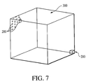
- FIG. 7 is an isomeric view of a photonic crystal comprising an array of unit cells formed of a second material in a first material and according to methods of the present invention.
- FIG. 8 illustrates the cubic P unit cell of FIG. 6.
- FIG. 9 illustrates various processing steps for forming a cubic lattice of spherical regions of a second material in a first material according to methods of the present invention.
- FIGS 1 - 3 illustrate the formation of empty-spaced void patterns 50 , 23 , 33 in a silicon substrate 10 of ⁇ 100> crystal orientation.
- Empty spaces which are formed in silicon substrates and have various shapes, such as plates, spheres or pipes, may be formed as a result of the self-organizing migration properties on the silicon surface.
- an ambient atmosphere such as a hydrogen ambient
- the silicon atoms on the surface migrate so that their surface energy is minimized.
- Sato et al. have demonstrated that the geometry of empty spaces, such as sphere, plate and pipe, formed under the surface of a silicon substrate depends on the size, number and spacing of a plurality of cylindrical holes that are initially formed at temperatures lower than the melting temperature of silicon.
- FIGS. 1 ( a )-( f ) illustrate how a single sphere-shaped empty space 50 is formed from a single cylindrical hole 12 formed within the silicon substrate 10 .
- the silicon substrate 10 is annealed at a temperature lower than the melting point of monocrystalline silicon (1400° C.), for example, at a temperature of about 1100° C. Sato et al. have demonstrated that, within about 60 seconds and under a reducing ambient of 10 Torr of hydrogen, the shape and surface morphology of the cylindrical hole 12 changes drastically to that of the sphere-shaped empty space 50 (FIG. 1( f )).
- the cylindrical hole 12 is unstable beyond a critical length Lc and transforms, therefore, to a lower energy state consisting of one or more empty spheres formed along the original cylinder axis.
- the number N of empty spheres that form from a cylindrical hole depends both on the length L of the cylindrical hole and on the cylinder radius Rc. Accordingly, the number N of empty spheres formed from a cylindrical hole made in a silicon substrate can be estimated according to the following equation:
- N number of empty spheres
- Rc radius of cylindrical hole
- L length of cylindrical hole.
- Rc radius of cylindrical hole.
- Rc radius of cylindrical hole.
- FIGS. 2 ( a )-( c ) which exemplify the formation of a single pipe-shaped empty space 23 from a linear array of cylindrical holes 22 .
- FIGS. 3 ( a )-( b ) illustrate the formation of a single plate-shaped empty space 33 from a two-dimensional array of cylindrical holes 32 formed within a silicon substrate such as the silicon substrate 10 .
- the values of the pipe radius Rp (of the pipe-shaped empty space 23 ) and that of the plate thickness Tp (of the plate-shaped empty space 33 ) may be calculated in a manner similar to that described above with reference to the formation of the empty sphere 50 and the calculation of sphere radius Rs in equation (1).
- the distance ⁇ between the centers of any two adjacent cylindrical holes 22 , 32 , in a linear array may be calculated from the following formula:
- Rc radius of cylindrical hole
- ⁇ center-to-center distance between two adjacent cylindrical holes in a linear array.
- Equation (4) ensures that adjacent cylindrical holes 22 , 32 do not touch each other allowing, therefore, the formation of a plurality of adjacent spheres that combine to form the resulting pipe-shaped empty space 23 and plate-shaped empty space 33 .
- Rp pipe radius
- Tp plate thickness
- ⁇ center-to-center distance between two adjacent cylindrical holes in a linear array.
- FIGS. 1 ( a )-( f ) To illustrate the formation of an exemplary embodiment of a spatial region of a second material formed within a first solid material, the present invention will be explained with reference to the formation of a sphere of a second material formed within a first solid material by the technique similar to that described above with reference to FIGS. 1 ( a )-( f ).
- the invention may be used to form any spatial regions, patterns and geometries, such as the pipes and plates described above with reference to FIGS. 2 ( a )-( c ) and FIGS. 3 ( a )-( b ), and thus the invention is not limited to the formation of sphere-shaped regions.
- a linear cylindrical hole 120 is formed into a first solid material 100 as a first step in the formation of a sphere 190 (FIG. 4( d )) and a sphere 290 (FIG. 5( b )) of a second material embedded in the first solid material 100 .
- the linear cylindrical hole 120 (FIG. 4( a )) is drilled into the first solid material 100 from an upper surface 111 of the first solid material 100 to a depth L 1 , which also represents the length of the cylindrical hole 120 .
- Equation (1) the number of empty spheres N to be obtained from the single cylindrical hole 120 depends upon the cylinder radius Rc 1 and the length L 1 of the cylindrical hole 120 . Accordingly, a valid solution for the equation (1) for the relationship between the number of spheres N and the length L 1 of the cylindrical hole 120 is the following:
- N number of empty spheres formed from cylindrical hole 120 ;
- Rc 1 radius of cylindrical hole 120 ;
- L 1 length of cylindrical hole 120 .
- the first solid material 100 may be any solid state material, structure or combination of material/structure for which its optical, electronic, and acoustic properties, among others, can be modified by the formation of spatial patterns, or by the rearrangement of photonic energy bands, in such material, structure, or combination thereof.
- the term “material” is to be understood as including, for example, linear and non-linear optical materials, metals, semiconductors and insulators, acoustic materials, magnetic materials, ferroelectric materials, piezoelectric materials, and superconducting materials, among others.
- the term “material” is to be understood as including substrates formed of silicon, silicon-on-insulator, doped and undoped semiconductors, epitaxial layers of silicon supported by a base semiconductor foundation, and other semiconductor structures.
- the first solid material 100 is immersed into a liquid-phase melt 150 (FIG. 4( b )) of a second material.
- the second material of the liquid-phase melt 150 is selected so that its melting point temperature T M ( 150 ) is below the melting point temperature T M ( 100 ) of the first solid material 100 .
- T I melting point temperature
- the temperature of the liquid-phase melt 150 is increased to allow surface and volume diffusion to drive the transformation of the cylindrical hole 120 a filled with the second material into a sphere-shaped region 190 (FIG. 4( c )), which is filled with the second material of the liquid-phase melt 150 and embedded in the first solid material 100 .
- the temperature of the liquid-phase melt 150 is increased from the initial temperature T I to a second, final temperature T F which is below the melting temperature T M ( 100 ) of the first solid material 100 .
- Table 1 below illustrates the melting and boiling temperatures for few representative and non-limiting examples of materials which may be used in the invention. These material are aluminum (Al), germanium (Ge), silicon (Si) and silicon dioxide (SiO 2 ).
- Al Al 660° C. 2647° C. Ge 937° C. 2830° C. Si 1410° C. 2355° C. SiO 2 1600° C. 2230° C.
- the first solid material 100 is removed from the liquid-phase melt 150 .
- the temperature of the first solid material 100 is slowly decreased to below the melting temperature T M ( 150 ) of the liquid-phase melt 150 so that the sphere-shaped region 190 is completely formed and embedded within the first solid material 100 .
- a photonic crystal is formed where the transmission and the reflection of electromagnetic waves is significantly different from those of each individual material (that is, the first solid material and the second material).
- a complete photonic bandgap can result where the wavelength range within the complete gap light (electromagnetic waves) will not be propagated due to destructive interference, but will rather be totally reflected for all directions of propagation.
- FIG. 5 illustrates another embodiment of the present invention, according to which a deposition method is employed to fill the linear cylindrical hole 120 (FIG. 4( a )) as an alternative method to the liquid-phase melt immersion method described above with reference to FIGS. 4 ( b )- 4 ( d ).
- a deposition method is employed to fill in the cylindrical hole 120 with a second material 250 (FIG. 5( a )).
- the second material 250 is selected so that its melting temperature T M ( 250 ) is below the melting temperature T M ( 100 ) of the first solid material 100 .
- deposition methods such as, for example, a conventional chemical vapor deposition (CVD), plasma enhanced CVD (PECVD) or physical vapor deposition (PVD), among others, may be used to substantially fill in the cylindrical hole 120 of FIG. 4( a ) with the second material 250 (FIG. 5( a )).
- CVD chemical vapor deposition
- PECVD plasma enhanced CVD
- PVD physical vapor deposition
- the first material 100 as well as the second material 250 are heated up to a temperature T which is near or below the melting temperature T M ( 100 ) of the first material 100 , and at or above the melting temperature T M ( 250 ) of the second material 250 .
- the temperature increase in the first material 100 and in the second material 250 allow significant surface and volume diffusion in the second material 250 as well as in the first material 100 to drive the transformation of the cylindrical hole 120 filled with the melt of the second material 250 into a sphere-shaped region 290 (FIG. 5( b )), which is filled with the second material 250 and formed within the first material 100 .
- the temperature of the first solid material 100 is slowly decreased to a final temperature T F which is below the melting temperature T M ( 250 ) of the second solid material 250 so that the sphere shaped region 290 of the second material solidifies.
- the exemplary embodiments described above refer to the formation of a spatial region having a sphere-shaped configuration filled with a second material and embedded within a first solid material
- other geometries and spatial patterns or regions for example pipe-shaped or plate-shaped configurations, may be formed also, as desired and as illustrated in FIGS. 2 - 3 .
- the present invention is not limited to the formation of only one spatial region of a second material embedded within a first solid material, and the invention contemplates the formation of a plurality of such spatial regions within a first solid material.
- the plurality of spatial regions may have any of the sphere-, pipe- or plate-shaped configurations, or any combination of such configurations.
- the plurality of regions may all be formed simultaneously or may be formed subsequent to each other.
- all regions may contain a second material embedded within a first material.
- the regions may contain a plurality of different materials (for example, a second, third, fourth, etc, material) each embedded within the first solid material. For example, and in accordance with Table 1, if two regions are formed within a first material such as silicon dioxide, one of the two regions may be of aluminum embedded within silicon dioxide, whereas the other of the two spatial regions may be formed of germanium embedded within silicon dioxide.
- FIG. 6 illustrates the unit cells of fourteen primitive space lattices.
- unit cell is to be understood as including any of the known space lattice unit cells.
- FIG. 7 To illustrate the formation of an exemplary embodiment of such a photonic band structure material of a second material formed within a first solid material, the present invention will be explained with reference to the formation of a photonic crystal 300 (FIG. 7) formed of unit cells 200 (FIG. 7) having spheres of a second material embedded within a first solid material and formed by the technique described above with reference to FIGS. 4 ( a )-( d ).
- the present invention will be explained with reference to the formation of the cubic P unit cell of FIG. 6 with lattice constant “a 0 ” which is again depicted in FIG. 8.
- spheres of a second material are formed in a wafer of the first material, such that the x, y axes are in the plane of the wafer and the z axis is normal to the plane.
- the four cylindrical holes 42 a, 42 b, 42 c, 42 d are spaced apart along the x and y axes at a distance “a 0 ” which represents the lattice constant of the cubic unit cell 200 (FIG. 8).
- the first solid material 100 is immersed into a liquid-phase melt 150 (FIG. 9( b )) of a second material.
- the second material of the liquid-phase melt 150 is selected so that its melting point temperature T M ( 150 ) is below the melting point temperature T M ( 100 ) of the first solid material 100 .
- the temperature of the liquid-phase melt 150 is maintained at an initial temperature T I , which is above the melting temperature T M ( 150 ) of the melt 150 but well below the melting temperature T M ( 100 ) of the first solid material 100 .
- melt of the second material fills the cylindrical holes 42 a, 42 b, 42 c, 42 d to form cylindrical holes 42 a 1 , 42 b 1 , 42 c 1 , 42 d 1 (FIG. 9( b )) of the melt of the second material within the first solid material 100 .
- the temperature of the liquid-phase melt 150 is increased from the initial temperature T I to a second temperature T 2 which is near to, but below, the melting temperature T M ( 100 ) of the first solid material 100 .
- T 2 the melting temperature of the first solid material 100 .
- surface and volume diffusion drives the transformation of the cylinders 42 a 1 , 42 b 1 , 42 c 1 , 42 d 1 filled with the melt of the second material into sphere-shaped regions 50 a, 50 b, 50 c, 50 d, 51 a, 51 b, 51 c and 51 d (FIG. 9( c )) containing the melt of the second material.
- These sphere-shaped regions form the desired cubic unit cell 200 depicted in FIG. 8.
- the first solid material 100 is removed from the liquid-phase melt 150 (FIG. 9( c )) and allowed to cool below the melting temperature T M ( 150 ) of the liquid-phase melt 150 , thus allowing the sphere-shaped regions 50 a, 50 b, 50 c, 50 d, 51 a, 51 b, 51 c and 51 d of the second material to solidify within the first solid state material 100 .
- the spatial regions act as diffraction centers for energy particles, such as electromagnetic waves, photons, X rays, gamma rays, electrons, light particles, magnetic waves or elastic waves, among others.
- energy particles such as electromagnetic waves, photons, X rays, gamma rays, electrons, light particles, magnetic waves or elastic waves, among others.
- the periodicity of the spatial regions formed according to the present invention will dictate the wavelength in which the particular photonic material scatters.
- the distance of separation between adjacent spatial regions which is also the lattice constant “a 0 ,” may be chosen to have a particular value that would allow diffraction to occur at a particular wavelength. For example, if the value of “a 0 ” is very big, in fractions of centimeters, then the microwave spectrum occurs. Conversely, if the value of “a 0 ” is very small, in fractions of wavelength of light, then the optical range occurs. This way, by adjusting the value of “a 0 ” for a given solid material, one skilled in the art can predict when an allowed energy band or a forbidden energy band (phototnic bandgap) may occur in such solid material.
- a forbidden energy band phototnic bandgap
- the present invention provides a method for forming diffraction spatial patterns and regions of a second material, arranged in periodic form in the superlattices of a first solid material, that will modify the transmission and reflection properties of the first solid material, and consequently, the energy bands for light in such first solid material.
- the present invention contemplates the formation of the unit cell 200 of FIG. 9( d ), by methods other than the liquid-phase melt immersion, for example, by the deposition method described in detail above with reference to the formation of the spatial region 290 (FIG. 5( b )) filled with a second material and embedded within a first solid material.
- the unit cell 200 of FIG. 9( d ) contains only eight empty-spaced spheres per unit cell formed from four cylindrical holes, it must be understood that in fact any number of such cylindrical holes may be drilled so that any number of their corresponding spheres of second material may be formed in the superlattice of the first solid material 100 , as desired. Accordingly, although the method of the present invention has been explained with reference to the formation of only one cubic unit 200 (FIG. 9( d )), it must be obvious to those skilled in the art that in fact any number of such cubic units of a second material forming the photonic bandgap lattice may be formed within the first solid material 100 by methods of the present invention.
- FIG. 6 illustrates a plurality of conventional representative unit cells forming various space lattices, as described by C. Kittel in Introduction to Solid State Physics (J. Whiley & Sons, 3d Ed (1966)), which may be formed as spatial patterns of a second material embedded in a first solid material in accordance with the invention.
- the invention is not limited to the formation of a unit cell having the diffraction centers formed of spheres of a second material embedded within a first solid material, but other regions or patterns, for example pipes, such as the empty-space pipe 23 (FIG. 2), and/or plates, such as the empty-space plate 33 (FIG. 3), may be employed in any number or orientation and any combination to form the unit cells of FIG. 6.
- pipes such as the empty-space pipe 23 (FIG. 2)
- plates such as the empty-space plate 33 (FIG. 3)
- the invention has been described with reference to the formation of spheres of a second material embedded within a first solid material forming diffraction centers and having similar radii, the invention also contemplates the formation of spheres of two or more materials, having different radii.
- the spatial patterns and regions formed according to embodiments of the present invention act as diffraction centers not only for optical wavelengths, but for other energy particles, such as, for example, microwaves, photons, X rays, gamma rays, as well as for magnetic waves, elastic waves, electrons and/or ions, among others.
Abstract
Description
- The present invention relates to solid state materials and, in particular, to a novel method of forming spatial regions having various geometries in such solid state materials.
- Crystalline solid state materials, such as single-crystal semiconductors, are the basis of the current microelectronics industry. Each single crystalline solid is a periodic structure in space, with a basic repeating unit called the unit cell. Crystalline solids are characterized by a variety of properties, for example, electrical properties such as electrical conductivity or charge mobility, optical properties such as refractive index or speed of photons, thermal properties such as thermal conductivity or thermal expansion, mechanical properties such as stress or strain curves, and chemical properties such as resistance to corrosion or reaction consistency, among others.
- Over the past years, theoretical and experimental interests have focussed on controlling various properties of the solid state materials, for example, their optical and/or physical properties. As such, numerous photonic lattice experiments have been carried out to realize photonic bandgap effects at optical wavelength in periodic crystalline solids as a way of obtaining novel photonic properties in such solids. In one photonic lattice experiment, for example, Yablonovitch et al. (E. Yablonovitch. Phys. Rev. Lett., 58, 2059 (1987)) have suggested that the electromagnetic radiation propagating in periodic dielectric structures is similar to the electron waves propagating in a crystal. Yablonovitch et al. realized that setting up a periodic index of refraction pattern in a material can produce a band structure for electromagnetic waves where certain wavelengths can or cannot propagate, producing therefore the electromagnetic wave equivalent of a metal, semiconductor or insulator. If the wavelength is in the order of the dimensions of the crystal lattice, a photonic bandgap (a frequency range where photons are not allowed to propagate) can open up in two or three dimensions and lead to interesting phenomena, such as inhibition of spontaneous emission from an atom that radiates inside the photonic gap or frequency selective transmission and reflection. This way, for example, if a photonic crystal can be constructed to posses a full photonic bandgap, then a photonic insulator is created by artificially controlling the optical properties of the solid.
- Other experiments have been carried out to achieve composite crystalline materials with novel physical and chemical properties. For example, the morphology and the local chemistry order of crystalline solid materials, and thus the physical properties of such crystalline materials, have been successfully influenced by creating the so-called “disordered materials.” Disordered materials are defined as compositionally modulated materials characterized by the lack of regular and long-range periodicity, which is typical of crystalline solids. In the disordered materials, atoms or groups of atoms are disbursed through the material so that the constrains of periodicity which characterizes single crystalline materials are removed. As a result, it is now possible to place atoms in three dimensional configurations which were previously prohibited by the lattice constants of the crystalline materials. Accordingly, a whole new spectrum of semiconductor materials having novel physical, chemical and electrical properties has been made available to the semiconductor industry.
- One of the limitations inherent in the above-mentioned photonic lattice experiments is the requirement that the dimensions of the lattice must be in the same order of magnitude as the desired band gap wavelength, or in other words, the refractive index variations or discontinuities should have periodicities on the same scale as the wavelength. As the dimensions of the lattice must be in the same order of magnitude as the desired band gap wavelength, the scaling down to the interesting optical and infrared frequencies has posed problems due to the demanded regularity and uniformity of the photonic lattice. In addition, the fabrication of the “disordered materials” is technologically difficult, as it requires non-equilibrium manufacturing techniques to provide a local order and/or morphology different from that achieved with equilibrium techniques. Further, the crystalline cells of the “disordered materials” are relatively thick because of their low absorption and, consequently, they are fragile, expensive and bulky.
- Accordingly, there is a need for an improved method of synthesizing new and broad classes of composite materials which have unique photonic, electronic, magnetic, acoustic or superconducting properties that are significantly different from the properties of the materials from which they are formed. There is also a need for fabricating various spatial patterns and/or geometries in solid state materials to improve the photonic, electronic, magnetic, acoustic or superconducting properties of such solid state materials. There is further a need for an improved method of fabricating three-dimensional photonic bandgap structures in a wide variety of solid materials, such as monocrystalline substrates, dielectrics, superconducting materials or magnetic materials, among others. There is also a need for a more advantageous method of generating a wide variety of space group symmetries, with different group symmetries for wavelength regions of interests, in such variety of solid materials.
- The present invention provides a method of forming various spatial patterns and geometries in solid state materials, as well as method of forming periodic index of refraction patterns in the supperlattice of a solid material to achieve photonic bandgap effects at desired optical wavelengths.
- According to an exemplary embodiment of the invention, at least one spatial region of a second material is formed by surface transformation in a first solid material, for example in a monocrystalline silicon substrate or an insulator, to control the optical and electromagnetic properties of such first solid material. The spatial regions of the second material include at least one region which is formed in the first solid material by drilling holes to a predefined depth and at a predefined lattice position. The first solid material is then immersed in a melt of the second material and held at a temperature below the melting point of the first solid material. The temperature of the melt of the second solid material is subsequently increased to a temperature close to the melting point of the first solid material to spontaneously form the spatial region filled with the second material and embedded in the first solid material at the desired location. The spatial region filled with the second material which is embedded in the first solid material may have various geometries and sizes.
- According to another exemplary embodiment of the invention, at least one spatial region of a second material is formed by surface transformation in a first solid material, for example in a monocrystalline silicon substrate or an insulator, to control the optical and electromagnetic properties of such first solid material. The spatial regions of the second material include at least one region which is formed in the first solid material by drilling holes to a predefined depth and at a predefined lattice position. The holes in the first solid material are subsequently filled with a second material by employing a deposition method, for example, chemical vapor deposition. The temperature of the first and second materials is subsequently increased to a temperature close to the melting point of the first solid material to spontaneously form the spatial region filled with the second material and embedded in the first solid material at the desired location. The spatial region filled with the second material which is embedded in the first solid material may have various geometries and sizes.
- According to yet another embodiment of the invention, a plurality of space group symmetries of a second material are formed by surface transformation in a first solid material, for example in a monocrystalline silicon substrate or an insulator, to control the optical and electromagnetic properties of such first solid material. The space group symmetries of the second material includes a plurality of spatial regions filled with the second material, which are formed in the first solid material by drilling holes to a predefined depth and at a predefined lattice position. The first solid material is then immersed in a melt of the second solid material and held at a temperature below the melting point of the first solid material. The temperature of the melt of the second material is subsequently increased to a temperature close to the melting point of the first solid material to spontaneously form the space group symmetries filled with the second material and embedded in the first solid material at the desired location. Alternatively, a deposition method, for example, chemical vapor deposition, may be employed to fill in the holes. The space group symmetries filled with the second material which are embedded in the first solid material may have various geometries and sizes, and may be formed at different periodicities and in a variety of space group symmetries, so that photonic bandgap structures can be produced for wavelength regions of interest.
- These and other features and advantages of the invention will be more clearly apparent from the following detailed description which is provided in connection with accompanying drawings and which illustrates exemplary embodiments of the invention.
- FIG. 1 illustrates a portion of a silicon substrate undergoing a sequence of steps for empty-spaced sphere formation.
- FIG. 2 illustrates a portion of a silicon substrate undergoing a sequence of steps for empty-spaced pipe formation.
- FIG. 3 illustrates a portion of a silicon substrate undergoing a sequence of steps for empty-spaced plate formation.
- FIG. 4 illustrates three-dimensional views of a spherical region of a second material formed within a first material and according to a first embodiment of the present invention.
- FIG. 5 illustrates three-dimensional views of a spherical region of a second material formed within a first material and according to a second embodiment of the present invention.
- FIG. 6 illustrates fourteen representative unit cells of space lattices which can be constructed according to the methods of the present invention.
- FIG. 7 is an isomeric view of a photonic crystal comprising an array of unit cells formed of a second material in a first material and according to methods of the present invention.
- FIG. 8 illustrates the cubic P unit cell of FIG. 6.
- FIG. 9 illustrates various processing steps for forming a cubic lattice of spherical regions of a second material in a first material according to methods of the present invention.
- In the following detailed description, reference is made to various exemplary embodiments for carrying out the invention. These embodiments are described with sufficient detail to enable those skilled in the art to practice the invention, and it is to be understood that other embodiments may be employed, and that structural, electrical and process changes may be made, and equivalents substituted, without departing from the invention. Accordingly, the following detailed description is exemplary and the scope of the present invention is not limited by the detailed description but is defined solely by the appended claims.
- In the exemplary embodiments described in detail below, reference will be made to a first solid material which is employed to form various spatial patterns and regions embedded in such first solid material for interacting with optical wavelengths. These various spatial regions and/or patterns are formed by an analogous method to that employed in the formation of empty-spaced void patterns in a silicon substrate. Accordingly, reference is made first to FIGS 1-3 which illustrate the formation of empty-
spaced void patterns silicon substrate 10 of <100> crystal orientation. Techniques for the formation of empty-spaced (void) patterns of different geometries in silicon are described by Sato et al., in Substrate Engineering for the Formation of Empty Space in Silicon (ESS) Induced by Silicon Surface Migration, 1999 IEDM Digest, Paper 20.6.1, the disclosure of which is incorporated by reference herein. - Empty spaces which are formed in silicon substrates and have various shapes, such as plates, spheres or pipes, may be formed as a result of the self-organizing migration properties on the silicon surface. As such, when deeply-etched silicon substrates are annealed in an ambient atmosphere, such as a hydrogen ambient, for example, the silicon atoms on the surface migrate so that their surface energy is minimized. Based on these findings, Sato et al. have demonstrated that the geometry of empty spaces, such as sphere, plate and pipe, formed under the surface of a silicon substrate depends on the size, number and spacing of a plurality of cylindrical holes that are initially formed at temperatures lower than the melting temperature of silicon.
- For example, FIGS. 1(a)-(f) illustrate how a single sphere-shaped
empty space 50 is formed from a singlecylindrical hole 12 formed within thesilicon substrate 10. Subsequent to the formation of thecylindrical hole 12, thesilicon substrate 10 is annealed at a temperature lower than the melting point of monocrystalline silicon (1400° C.), for example, at a temperature of about 1100° C. Sato et al. have demonstrated that, within about 60 seconds and under a reducing ambient of 10 Torr of hydrogen, the shape and surface morphology of thecylindrical hole 12 changes drastically to that of the sphere-shaped empty space 50 (FIG. 1(f)). Because of the significant surface and/or volume diffusion which occurs at high annealing temperatures, thecylindrical hole 12 is unstable beyond a critical length Lc and transforms, therefore, to a lower energy state consisting of one or more empty spheres formed along the original cylinder axis. - As analyzed by Nichols et al., in Surface- (Interface-) and Volume-Diffusion Contributions to Morphological Changes Driven by Capillarity, Trans. AIME 233 at 1840 (October 1965), the disclosure of which is incorporated by reference herein, the number N of empty spheres that form from a cylindrical hole depends both on the length L of the cylindrical hole and on the cylinder radius Rc. Accordingly, the number N of empty spheres formed from a cylindrical hole made in a silicon substrate can be estimated according to the following equation:
- 8.89RcN≦L<8.89Rc(N+1) (1)
- wherein: N=number of empty spheres;
- Rc=radius of cylindrical hole; and
- L=length of cylindrical hole.
- Thus, equation (1) predicts that, if L<8.89 Rc, the number of empty spheres will be N=0, which means that no empty spheres will form from a cylindrical hole.
- When one or more empty spheres form with a radius Rs, then according to Nichols et al., the value of Rs is given by the following equation:
- Rs=1.88Rc (2)
- wherein: Rs=sphere radius; and
- Rc=radius of cylindrical hole.
- When two or more empty spheres form from a cylinder hole with a cylinder radius Rc, then the distance “1” between the centers of two adjacent empty-spaced spheres is calculated from the following formula:
- 1=8.89Rc (3)
- wherein: 1=center-to-center distance between two adjacent spheres; and
- Rc=radius of cylindrical hole.
- Reference is now made to FIGS. 2(a)-(c), which exemplify the formation of a single pipe-shaped
empty space 23 from a linear array ofcylindrical holes 22. Similarly, FIGS. 3(a)-(b) illustrate the formation of a single plate-shapedempty space 33 from a two-dimensional array ofcylindrical holes 32 formed within a silicon substrate such as thesilicon substrate 10. The values of the pipe radius Rp (of the pipe-shaped empty space 23) and that of the plate thickness Tp (of the plate-shaped empty space 33) may be calculated in a manner similar to that described above with reference to the formation of theempty sphere 50 and the calculation of sphere radius Rs in equation (1). The distance Δ between the centers of any two adjacentcylindrical holes - 2Rc<Δ<3.76Rc (4)
- wherein: Rc=radius of cylindrical hole; and
- Δ=center-to-center distance between two adjacent cylindrical holes in a linear array.
- Equation (4) ensures that adjacent
cylindrical holes empty space 23 and plate-shapedempty space 33. - The values of the pipe radius Rp and of the plate thickness Tp are given by the following two expressions:
- Rp=(8.86Rc3/Δ)1/2 (5)
- Tp=27.83Rc3/Δ2 (6)
- wherein: Rp=pipe radius;
- Tp=plate thickness; and
- Δ=center-to-center distance between two adjacent cylindrical holes in a linear array.
- To illustrate the formation of an exemplary embodiment of a spatial region of a second material formed within a first solid material, the present invention will be explained with reference to the formation of a sphere of a second material formed within a first solid material by the technique similar to that described above with reference to FIGS. 1(a)-(f). However, it must be understood that the invention may be used to form any spatial regions, patterns and geometries, such as the pipes and plates described above with reference to FIGS. 2(a)-(c) and FIGS. 3(a)-(b), and thus the invention is not limited to the formation of sphere-shaped regions.
- Referring now to FIG. 4( a), a linear
cylindrical hole 120 is formed into a firstsolid material 100 as a first step in the formation of a sphere 190 (FIG. 4(d)) and a sphere 290 (FIG. 5(b)) of a second material embedded in the firstsolid material 100. The linear cylindrical hole 120 (FIG. 4(a)) is drilled into the firstsolid material 100 from anupper surface 111 of the firstsolid material 100 to a depth L1, which also represents the length of thecylindrical hole 120. - Applying equation (1) to the parameters of the linear
cylindrical hole 120, the number of empty spheres N to be obtained from the singlecylindrical hole 120 depends upon the cylinder radius Rc1 and the length L1 of thecylindrical hole 120. Accordingly, a valid solution for the equation (1) for the relationship between the number of spheres N and the length L1 of thecylindrical hole 120 is the following: - L1=8.89Rc1N (7)
- wherein: N=number of empty spheres formed from
cylindrical hole 120; - Rc 1=radius of
cylindrical hole 120; and - L 1=length of
cylindrical hole 120. - Accordingly, if one sphere is desired from the
cylindrical hole 120, then the radius Rc of thecylindrical hole 120 and the depth L1 satisfies equation (7) above for N=1. - The first
solid material 100 may be any solid state material, structure or combination of material/structure for which its optical, electronic, and acoustic properties, among others, can be modified by the formation of spatial patterns, or by the rearrangement of photonic energy bands, in such material, structure, or combination thereof. Thus, the term “material” is to be understood as including, for example, linear and non-linear optical materials, metals, semiconductors and insulators, acoustic materials, magnetic materials, ferroelectric materials, piezoelectric materials, and superconducting materials, among others. In addition, the term “material” is to be understood as including substrates formed of silicon, silicon-on-insulator, doped and undoped semiconductors, epitaxial layers of silicon supported by a base semiconductor foundation, and other semiconductor structures. - Referring now to FIG. 4( b), subsequent to the formation of
cylindrical hole 120 in the firstsolid material 100, the firstsolid material 100 is immersed into a liquid-phase melt 150 (FIG. 4(b)) of a second material. The second material of the liquid-phase melt 150 is selected so that its melting point temperature TM(150) is below the melting point temperature TM(100) of the firstsolid material 100. This way, during the immersion step, the temperature of the liquid-phase melt 150 is maintained at an initial temperature TI, which is above the melting temperature TM(150) of the liquid-phase melt 150, but well below the melting temperature TM(100) of the firstsolid material 100. As a consequence, parts of the liquid-phase melt 150 fill thecylindrical hole 120 to form acylindrical hole 120 a (FIG. 4(b)) filled with the second material and formed within the firstsolid material 100. - Subsequent to the formation of the
cylindrical hole 120 a (FIG. 4(b)) filled with the second material, the temperature of the liquid-phase melt 150 is increased to allow surface and volume diffusion to drive the transformation of thecylindrical hole 120 a filled with the second material into a sphere-shaped region 190 (FIG. 4(c)), which is filled with the second material of the liquid-phase melt 150 and embedded in the firstsolid material 100. During this processing step, the temperature of the liquid-phase melt 150 is increased from the initial temperature TI to a second, final temperature TF which is below the melting temperature TM(100) of the firstsolid material 100. Table 1 below illustrates the melting and boiling temperatures for few representative and non-limiting examples of materials which may be used in the invention. These material are aluminum (Al), germanium (Ge), silicon (Si) and silicon dioxide (SiO2).TABLE 1 TM TB Al 660° C. 2647° C. Ge 937° C. 2830° C. Si 1410° C. 2355° C. SiO2 1600° C. 2230° C. - It is evident from the data of Table 1 that, for the above four mentioned materials, it is possible to form (1) an aluminum sphere-shaped
region 190 in germanium, an aluminum sphere-shapedregion 190 in silicon, or an aluminum sphere-shapedregion 190 in silicon dioxide; (2) a germanium sphere-shapedregion 190 in silicon or a germanium sphere-shapedregion 190 in silicon dioxide; and (3) a silicon sphere-shapedregion 190 in silicon dioxide. - Referring to FIG. 4( d), subsequent to the formation of the sphere-shaped region 190 (FIG. 4(c)) filled with the second material of the liquid-
phase melt 150 and embedded in the firstsolid material 100, the firstsolid material 100 is removed from the liquid-phase melt 150. The temperature of the firstsolid material 100 is slowly decreased to below the melting temperature TM(150) of the liquid-phase melt 150 so that the sphere-shapedregion 190 is completely formed and embedded within the firstsolid material 100. This way, for example, if the embedded second material and the firstsolid material 100 have different indices of refraction, then a photonic crystal is formed where the transmission and the reflection of electromagnetic waves is significantly different from those of each individual material (that is, the first solid material and the second material). In addition, for certain choices of index difference, crystal symmetry and periodicity, a complete photonic bandgap can result where the wavelength range within the complete gap light (electromagnetic waves) will not be propagated due to destructive interference, but will rather be totally reflected for all directions of propagation. - FIG. 5 illustrates another embodiment of the present invention, according to which a deposition method is employed to fill the linear cylindrical hole 120 (FIG. 4(a)) as an alternative method to the liquid-phase melt immersion method described above with reference to FIGS. 4(b)-4(d). Referring now to FIG. 4(a) and FIG. 5(a), subsequent to the formation of the cylindrical hole 120 (FIG. 4(a)) in the first
solid material 100, a deposition method is employed to fill in thecylindrical hole 120 with a second material 250 (FIG. 5(a)). Thesecond material 250 is selected so that its melting temperature TM(250) is below the melting temperature TM(100) of the firstsolid material 100. - In an exemplary embodiment of the invention, deposition methods such as, for example, a conventional chemical vapor deposition (CVD), plasma enhanced CVD (PECVD) or physical vapor deposition (PVD), among others, may be used to substantially fill in the
cylindrical hole 120 of FIG. 4(a) with the second material 250 (FIG. 5(a)). Subsequent to the deposition of thesecond material 250, thefirst material 100 as well as thesecond material 250 are heated up to a temperature T which is near or below the melting temperature TM(100) of thefirst material 100, and at or above the melting temperature TM(250) of thesecond material 250. The temperature increase in thefirst material 100 and in thesecond material 250 allow significant surface and volume diffusion in thesecond material 250 as well as in thefirst material 100 to drive the transformation of thecylindrical hole 120 filled with the melt of thesecond material 250 into a sphere-shaped region 290 (FIG. 5(b)), which is filled with thesecond material 250 and formed within thefirst material 100. Finally, the temperature of the firstsolid material 100 is slowly decreased to a final temperature TF which is below the melting temperature TM(250) of the secondsolid material 250 so that the sphere shapedregion 290 of the second material solidifies. - Although the exemplary embodiments described above refer to the formation of a spatial region having a sphere-shaped configuration filled with a second material and embedded within a first solid material, it must be understood that other geometries and spatial patterns or regions, for example pipe-shaped or plate-shaped configurations, may be formed also, as desired and as illustrated in FIGS. 2-3. In addition, the present invention is not limited to the formation of only one spatial region of a second material embedded within a first solid material, and the invention contemplates the formation of a plurality of such spatial regions within a first solid material. Further, the plurality of spatial regions may have any of the sphere-, pipe- or plate-shaped configurations, or any combination of such configurations. The plurality of regions may all be formed simultaneously or may be formed subsequent to each other. In one embodiment, all regions may contain a second material embedded within a first material. In another embodiment, the regions may contain a plurality of different materials (for example, a second, third, fourth, etc, material) each embedded within the first solid material. For example, and in accordance with Table 1, if two regions are formed within a first material such as silicon dioxide, one of the two regions may be of aluminum embedded within silicon dioxide, whereas the other of the two spatial regions may be formed of germanium embedded within silicon dioxide.
- According to another embodiment of the invention, a plurality of space group symmetries of a second material are formed in the superlattice of a first solid material, to achieve photonic band effects at desired optical wavelengths. FIG. 6 illustrates the unit cells of fourteen primitive space lattices. For the purposes of the present invention, the term “unit cell” is to be understood as including any of the known space lattice unit cells.
- To illustrate the formation of an exemplary embodiment of such a photonic band structure material of a second material formed within a first solid material, the present invention will be explained with reference to the formation of a photonic crystal 300 (FIG. 7) formed of unit cells 200 (FIG. 7) having spheres of a second material embedded within a first solid material and formed by the technique described above with reference to FIGS. 4(a)-(d). For simplicity, the present invention will be explained with reference to the formation of the cubic P unit cell of FIG. 6 with lattice constant “a0” which is again depicted in FIG. 8. In the present application, we assume that spheres of a second material are formed in a wafer of the first material, such that the x, y axes are in the plane of the wafer and the z axis is normal to the plane. To form spheres of the second material at each of the unit cell lattice positions in FIG. 8, it is necessary to drill a defined set of cylindrical holes into the wafer of the first material.
- For simplicity, the formation of one unit cell in (x, y) direction and of n unit cells in the z-direction will be now discussed. To form additional unit cells in the (x,y) plane, repeated translation of the hole pattern in the x and y direction is all that is required. From equations (2) and (3) above, it is known that to create spheres with periodicity a 0 in the z-direction requires that the radius Rc of the cylindrical holes must be Rc=a0/8.89≅0.11a0 and after surface transformation the radius Rs of each formed sphere of the second material will be Rs=(1.88/8.99)a0≅0.212a0. Accordingly, the depth Ln of the initial cylindrical holes that will form by surface transformation for n unit cells in the z-direction is
- Ln=(n+1)a 0=(n+1)(8.89)Rc (8)
- To form a single unit cell (i.e. two spheres) in the z-direction, as it will be described below, the required hole depth is L 1=2 (8.89) Rc.
- Referring now to FIG. 9, during the first step in the formation of the cubic unit 200 (FIG. 8), four linear
cylindrical holes solid material 100 from anupper surface 111 of the firstsolid material 100 to a depth L1=2a0. The fourcylindrical holes - Subsequent to the formation of
cylindrical holes solid material 100, the firstsolid material 100 is immersed into a liquid-phase melt 150 (FIG. 9(b)) of a second material. The second material of the liquid-phase melt 150 is selected so that its melting point temperature TM(150) is below the melting point temperature TM(100) of the firstsolid material 100. During the immersion step, the temperature of the liquid-phase melt 150 is maintained at an initial temperature TI, which is above the melting temperature TM(150) of themelt 150 but well below the melting temperature TM(100) of the firstsolid material 100. This way, melt of the second material fills thecylindrical holes cylindrical holes 42 a 1, 42b 1, 42 c 1, 42 d 1 (FIG. 9(b)) of the melt of the second material within the firstsolid material 100. - After the formation of the
cylindrical holes 42 a 1, 42b 1, 42 c 1, 42 d 1 (FIG. 9(b)), the temperature of the liquid-phase melt 150 is increased from the initial temperature TI to a second temperature T2 which is near to, but below, the melting temperature TM(100) of the firstsolid material 100. At this second temperature T2 surface and volume diffusion drives the transformation of thecylinders 42 a 1, 42b 1, 42 c 1, 42 d 1 filled with the melt of the second material into sphere-shapedregions cubic unit cell 200 depicted in FIG. 8. - Finally, referring to FIG. 9( d), the first
solid material 100 is removed from the liquid-phase melt 150 (FIG. 9(c)) and allowed to cool below the melting temperature TM(150) of the liquid-phase melt 150, thus allowing the sphere-shapedregions solid state material 100. - By arranging the spatial regions (for example, the
spheres cubic unit 200 of FIG. 9(d)) in a substrate photonic material (for example, the first solid material 100), the spatial regions act as diffraction centers for energy particles, such as electromagnetic waves, photons, X rays, gamma rays, electrons, light particles, magnetic waves or elastic waves, among others. The periodicity of the spatial regions formed according to the present invention will dictate the wavelength in which the particular photonic material scatters. Accordingly, the distance of separation between adjacent spatial regions, which is also the lattice constant “a0,” may be chosen to have a particular value that would allow diffraction to occur at a particular wavelength. For example, if the value of “a0” is very big, in fractions of centimeters, then the microwave spectrum occurs. Conversely, if the value of “a0” is very small, in fractions of wavelength of light, then the optical range occurs. This way, by adjusting the value of “a0” for a given solid material, one skilled in the art can predict when an allowed energy band or a forbidden energy band (phototnic bandgap) may occur in such solid material. - Thus, the present invention provides a method for forming diffraction spatial patterns and regions of a second material, arranged in periodic form in the superlattices of a first solid material, that will modify the transmission and reflection properties of the first solid material, and consequently, the energy bands for light in such first solid material.
- Although the embodiment illustrated above with reference to FIG. 9 has been described with reference to the formation of regions of a second material embedded within a first material by the liquid-phase melt immersion method, the above-illustrated embodiment is not limited to the immersion method. Accordingly, the present invention contemplates the formation of the
unit cell 200 of FIG. 9(d), by methods other than the liquid-phase melt immersion, for example, by the deposition method described in detail above with reference to the formation of the spatial region 290 (FIG. 5(b)) filled with a second material and embedded within a first solid material. - Although the
unit cell 200 of FIG. 9(d) contains only eight empty-spaced spheres per unit cell formed from four cylindrical holes, it must be understood that in fact any number of such cylindrical holes may be drilled so that any number of their corresponding spheres of second material may be formed in the superlattice of the firstsolid material 100, as desired. Accordingly, although the method of the present invention has been explained with reference to the formation of only one cubic unit 200 (FIG. 9(d)), it must be obvious to those skilled in the art that in fact any number of such cubic units of a second material forming the photonic bandgap lattice may be formed within the firstsolid material 100 by methods of the present invention. - Although the exemplary embodiments described above refer to the formation of a lattice of unit cells having a specific cubic configuration, it must be understood that other lattices of unit cells may be formed, depending on the characteristics of the particular lattice and photonic bandgap structure to be fabricated. As noted above, FIG. 6 illustrates a plurality of conventional representative unit cells forming various space lattices, as described by C. Kittel in Introduction to Solid State Physics (J. Whiley & Sons, 3d Ed (1966)), which may be formed as spatial patterns of a second material embedded in a first solid material in accordance with the invention.
- Further, the invention is not limited to the formation of a unit cell having the diffraction centers formed of spheres of a second material embedded within a first solid material, but other regions or patterns, for example pipes, such as the empty-space pipe 23 (FIG. 2), and/or plates, such as the empty-space plate 33 (FIG. 3), may be employed in any number or orientation and any combination to form the unit cells of FIG. 6. In addition, although the invention has been described with reference to the formation of spheres of a second material embedded within a first solid material forming diffraction centers and having similar radii, the invention also contemplates the formation of spheres of two or more materials, having different radii. Finally, the spatial patterns and regions formed according to embodiments of the present invention act as diffraction centers not only for optical wavelengths, but for other energy particles, such as, for example, microwaves, photons, X rays, gamma rays, as well as for magnetic waves, elastic waves, electrons and/or ions, among others.
- The above description and drawings are only to be considered illustrative of exemplary embodiments which achieve the features and advantages of the present invention. Modification and substitutions to specific process conditions and structures can be made without departing from the spirit and scope of the present invention. Accordingly, the invention is not to be considered as being limited by the foregoing description and drawings, but is only limited by the scope of the appended claims.
Claims (86)
Priority Applications (2)
| Application Number | Priority Date | Filing Date | Title |
|---|---|---|---|
| US10/118,350 US7022604B2 (en) | 2002-04-09 | 2002-04-09 | Method of forming spatial regions of a second material in a first material |
| US10/628,243 US6894309B2 (en) | 2002-04-09 | 2003-07-29 | Spatial regions of a second material in a first material |
Applications Claiming Priority (1)
| Application Number | Priority Date | Filing Date | Title |
|---|---|---|---|
| US10/118,350 US7022604B2 (en) | 2002-04-09 | 2002-04-09 | Method of forming spatial regions of a second material in a first material |
Related Child Applications (1)
| Application Number | Title | Priority Date | Filing Date |
|---|---|---|---|
| US10/628,243 Division US6894309B2 (en) | 2002-04-09 | 2003-07-29 | Spatial regions of a second material in a first material |
Publications (2)
| Publication Number | Publication Date |
|---|---|
| US20030190796A1 true US20030190796A1 (en) | 2003-10-09 |
| US7022604B2 US7022604B2 (en) | 2006-04-04 |
Family
ID=28674407
Family Applications (2)
| Application Number | Title | Priority Date | Filing Date |
|---|---|---|---|
| US10/118,350 Expired - Lifetime US7022604B2 (en) | 2002-04-09 | 2002-04-09 | Method of forming spatial regions of a second material in a first material |
| US10/628,243 Expired - Fee Related US6894309B2 (en) | 2002-04-09 | 2003-07-29 | Spatial regions of a second material in a first material |
Family Applications After (1)
| Application Number | Title | Priority Date | Filing Date |
|---|---|---|---|
| US10/628,243 Expired - Fee Related US6894309B2 (en) | 2002-04-09 | 2003-07-29 | Spatial regions of a second material in a first material |
Country Status (1)
| Country | Link |
|---|---|
| US (2) | US7022604B2 (en) |
Cited By (3)
| Publication number | Priority date | Publication date | Assignee | Title |
|---|---|---|---|---|
| US20050017273A1 (en) * | 2003-07-21 | 2005-01-27 | Micron Technology, Inc. | Gettering using voids formed by surface transformation |
| US7964124B2 (en) | 2002-01-17 | 2011-06-21 | Micron Technology, Inc. | Method of forming cellular material |
| US7989311B2 (en) | 2003-07-21 | 2011-08-02 | Micron Technlogy, Inc. | Strained semiconductor by full wafer bonding |
Families Citing this family (2)
| Publication number | Priority date | Publication date | Assignee | Title |
|---|---|---|---|---|
| FI20051143A0 (en) * | 2005-11-10 | 2005-11-10 | Artto Mikael Aurola | Method of manufacturing a semiconductor device |
| US10169322B2 (en) * | 2016-05-03 | 2019-01-01 | Dinky Labs, LLC | Personal dictionary |
Citations (15)
| Publication number | Priority date | Publication date | Assignee | Title |
|---|---|---|---|---|
| US4503447A (en) * | 1982-07-16 | 1985-03-05 | The United States Of America As Represented By The Secretary Of The Army | Multi-dimensional quantum well device |
| US4603232A (en) * | 1984-09-24 | 1986-07-29 | Npd Research, Inc. | Rapid market survey collection and dissemination method |
| US5645684A (en) * | 1994-03-07 | 1997-07-08 | The Regents Of The University Of California | Multilayer high vertical aspect ratio thin film structures |
| US5796207A (en) * | 1997-04-28 | 1998-08-18 | Rutgers, The State University Of New Jersey | Oriented piezo electric ceramics and ceramic/polymer composites |
| US5842195A (en) * | 1994-09-14 | 1998-11-24 | Dolphin Software Pty Ltd | Method and apparatus for preparation of a database document in a local processing apparatus and loading of the database document with data from remote sources |
| US5990850A (en) * | 1995-03-17 | 1999-11-23 | Massachusetts Institute Of Technology | Metallodielectric photonic crystal |
| US6070143A (en) * | 1997-12-05 | 2000-05-30 | Lucent Technologies Inc. | System and method for analyzing work requirements and linking human resource products to jobs |
| US6261469B1 (en) * | 1998-10-13 | 2001-07-17 | Honeywell International Inc. | Three dimensionally periodic structural assemblies on nanometer and longer scales |
| US6358854B1 (en) * | 1999-04-21 | 2002-03-19 | Sandia Corporation | Method to fabricate layered material compositions |
| US6392787B1 (en) * | 2000-09-01 | 2002-05-21 | Agere Systems Guardian Corp. | Process for fabricating article comprising photonic band gap material |
| US6433931B1 (en) * | 1997-02-11 | 2002-08-13 | Massachusetts Institute Of Technology | Polymeric photonic band gap materials |
| US6476409B2 (en) * | 1999-04-27 | 2002-11-05 | Canon Kabushiki Kaisha | Nano-structures, process for preparing nano-structures and devices |
| US6544808B2 (en) * | 2000-03-04 | 2003-04-08 | Nmctek Co., Ltd. | Light-emitting device with quantum dots and holes, and its fabricating method |
| US6582512B2 (en) * | 2001-05-22 | 2003-06-24 | Micron Technology, Inc. | Method of forming three-dimensional photonic band structures in solid materials |
| US6611085B1 (en) * | 2001-08-27 | 2003-08-26 | Sandia Corporation | Photonically engineered incandescent emitter |
Family Cites Families (5)
| Publication number | Priority date | Publication date | Assignee | Title |
|---|---|---|---|---|
| US5440421A (en) | 1994-05-10 | 1995-08-08 | Massachusetts Institute Of Technology | Three-dimensional periodic dielectric structures having photonic bandgaps |
| US5689275A (en) | 1995-05-16 | 1997-11-18 | Georgia Tech Research Corporation | Electromagnetic antenna and transmission line utilizing photonic bandgap material |
| US6477504B1 (en) | 1998-03-02 | 2002-11-05 | Ix, Inc. | Method and apparatus for automating the conduct of surveys over a network system |
| US6556974B1 (en) | 1998-12-30 | 2003-04-29 | D'alessandro Alex F. | Method for evaluating current business performance |
| AU2001295333A1 (en) | 2000-10-16 | 2002-04-29 | Hernan Miguez | Method of self-assembly and optical applications of crystalline colloidal patterns on substrates |
-
2002
- 2002-04-09 US US10/118,350 patent/US7022604B2/en not_active Expired - Lifetime
-
2003
- 2003-07-29 US US10/628,243 patent/US6894309B2/en not_active Expired - Fee Related
Patent Citations (15)
| Publication number | Priority date | Publication date | Assignee | Title |
|---|---|---|---|---|
| US4503447A (en) * | 1982-07-16 | 1985-03-05 | The United States Of America As Represented By The Secretary Of The Army | Multi-dimensional quantum well device |
| US4603232A (en) * | 1984-09-24 | 1986-07-29 | Npd Research, Inc. | Rapid market survey collection and dissemination method |
| US5645684A (en) * | 1994-03-07 | 1997-07-08 | The Regents Of The University Of California | Multilayer high vertical aspect ratio thin film structures |
| US5842195A (en) * | 1994-09-14 | 1998-11-24 | Dolphin Software Pty Ltd | Method and apparatus for preparation of a database document in a local processing apparatus and loading of the database document with data from remote sources |
| US5990850A (en) * | 1995-03-17 | 1999-11-23 | Massachusetts Institute Of Technology | Metallodielectric photonic crystal |
| US6433931B1 (en) * | 1997-02-11 | 2002-08-13 | Massachusetts Institute Of Technology | Polymeric photonic band gap materials |
| US5796207A (en) * | 1997-04-28 | 1998-08-18 | Rutgers, The State University Of New Jersey | Oriented piezo electric ceramics and ceramic/polymer composites |
| US6070143A (en) * | 1997-12-05 | 2000-05-30 | Lucent Technologies Inc. | System and method for analyzing work requirements and linking human resource products to jobs |
| US6261469B1 (en) * | 1998-10-13 | 2001-07-17 | Honeywell International Inc. | Three dimensionally periodic structural assemblies on nanometer and longer scales |
| US6358854B1 (en) * | 1999-04-21 | 2002-03-19 | Sandia Corporation | Method to fabricate layered material compositions |
| US6476409B2 (en) * | 1999-04-27 | 2002-11-05 | Canon Kabushiki Kaisha | Nano-structures, process for preparing nano-structures and devices |
| US6544808B2 (en) * | 2000-03-04 | 2003-04-08 | Nmctek Co., Ltd. | Light-emitting device with quantum dots and holes, and its fabricating method |
| US6392787B1 (en) * | 2000-09-01 | 2002-05-21 | Agere Systems Guardian Corp. | Process for fabricating article comprising photonic band gap material |
| US6582512B2 (en) * | 2001-05-22 | 2003-06-24 | Micron Technology, Inc. | Method of forming three-dimensional photonic band structures in solid materials |
| US6611085B1 (en) * | 2001-08-27 | 2003-08-26 | Sandia Corporation | Photonically engineered incandescent emitter |
Cited By (12)
| Publication number | Priority date | Publication date | Assignee | Title |
|---|---|---|---|---|
| US7964124B2 (en) | 2002-01-17 | 2011-06-21 | Micron Technology, Inc. | Method of forming cellular material |
| US20050017273A1 (en) * | 2003-07-21 | 2005-01-27 | Micron Technology, Inc. | Gettering using voids formed by surface transformation |
| US6929984B2 (en) | 2003-07-21 | 2005-08-16 | Micron Technology Inc. | Gettering using voids formed by surface transformation |
| US20050250274A1 (en) * | 2003-07-21 | 2005-11-10 | Micron Technology, Inc. | Gettering using voids formed by surface transformation |
| US20070075401A1 (en) * | 2003-07-21 | 2007-04-05 | Micron Technology, Inc. | Gettering using voids formed by surface transformation |
| US20070080335A1 (en) * | 2003-07-21 | 2007-04-12 | Micron Technology, Inc. | Gettering using voids formed by surface transformation |
| US7326597B2 (en) | 2003-07-21 | 2008-02-05 | Micron Technology, Inc. | Gettering using voids formed by surface transformation |
| US7544984B2 (en) | 2003-07-21 | 2009-06-09 | Micron Technology, Inc. | Gettering using voids formed by surface transformation |
| US7564082B2 (en) | 2003-07-21 | 2009-07-21 | Micron Technology, Inc. | Gettering using voids formed by surface transformation |
| US7989311B2 (en) | 2003-07-21 | 2011-08-02 | Micron Technlogy, Inc. | Strained semiconductor by full wafer bonding |
| US7994595B2 (en) | 2003-07-21 | 2011-08-09 | Micron Technology, Inc. | Strained semiconductor by full wafer bonding |
| US8470687B2 (en) | 2003-07-21 | 2013-06-25 | Micron Technology, Inc. | Strained semiconductor by full wafer bonding |
Also Published As
| Publication number | Publication date |
|---|---|
| US20040038527A1 (en) | 2004-02-26 |
| US6894309B2 (en) | 2005-05-17 |
| US7022604B2 (en) | 2006-04-04 |
Similar Documents
| Publication | Publication Date | Title |
|---|---|---|
| US6582512B2 (en) | Method of forming three-dimensional photonic band structures in solid materials | |
| US7260125B2 (en) | Method of forming mirrors by surface transformation of empty spaces in solid state materials | |
| US10109479B1 (en) | Method of making a semiconductor device with a buried insulating layer formed by annealing a superlattice | |
| US10170560B2 (en) | Semiconductor devices with enhanced deterministic doping and related methods | |
| US10727049B2 (en) | Method for making a semiconductor device including compound semiconductor materials and an impurity and point defect blocking superlattice | |
| US10468245B2 (en) | Semiconductor device including compound semiconductor materials and an impurity and point defect blocking superlattice | |
| US7333264B2 (en) | Photonic bandgap materials based on silicon | |
| CN102741999B (en) | Methods of fabricating semiconductor structures and devices using glass bonding layers, and semiconductor structures and devices formed by such methods | |
| CA2363277A1 (en) | Photonic band gap materials based on spiral posts in a lattice | |
| Marri et al. | Doped and codoped silicon nanocrystals: The role of surfaces and interfaces | |
| US20050029501A1 (en) | Low k interconnect dielectric using surface transformation | |
| US7018467B2 (en) | Three-dimensional complete bandgap photonic crystal formed by crystal modification | |
| US7022604B2 (en) | Method of forming spatial regions of a second material in a first material | |
| KR20230165390A (en) | Device and Method of Manufacturing AIII-BV-crystals and Substrate Wafers Manufactured Thereof Free of Residual Stress and Dislocations | |
| CN117413341A (en) | Semiconductor device including superlattice and enriched silicon 28 epitaxial layer and related methods | |
| US20220352322A1 (en) | Semiconductor device including a superlattice and enriched silicon 28 epitaxial layer | |
| Trifonov et al. | Analysis of photonic band gaps in two-dimensional photonic crystals with rods covered by a thin interfacial layer | |
| Gorelik et al. | Raman scattering in three-dimensional photonic crystals | |
| Cherkashin et al. | Control over the parameters of InAs-GaAs quantum dot arrays in the Stranski-Krastanow growth mode | |
| Kawashima et al. | Tailoring of the unit cell structure of autocloned photonic crystals | |
| EP3844819B1 (en) | Method for making superlattice structures with reduced defect densities | |
| Tatsumura et al. | Large-scale atomistic modeling of thermally grown SiO2 on Si (111) substrate | |
| TWI806553B (en) | Semiconductor device including a superlattice and enriched silicon 28 epitaxial layer and associated methods | |
| Mukaiyama et al. | Numerical Modeling and Evaluation of Constitutional Supercooling during Silicon Single Crystal Growth by Cz Method | |
| EP1279053A2 (en) | Photonic bandgap materials based on silicon |
Legal Events
| Date | Code | Title | Description |
|---|---|---|---|
| AS | Assignment |
Owner name: MICRON TECHNOLOGY, INC., IDAHO Free format text: ASSIGNMENT OF ASSIGNORS INTEREST;ASSIGNOR:GEUSIC, JOSEPH E.;REEL/FRAME:012786/0310 Effective date: 20020404 |
|
| STCF | Information on status: patent grant |
Free format text: PATENTED CASE |
|
| FEPP | Fee payment procedure |
Free format text: PAYOR NUMBER ASSIGNED (ORIGINAL EVENT CODE: ASPN); ENTITY STATUS OF PATENT OWNER: LARGE ENTITY |
|
| FPAY | Fee payment |
Year of fee payment: 4 |
|
| FPAY | Fee payment |
Year of fee payment: 8 |
|
| AS | Assignment |
Owner name: U.S. BANK NATIONAL ASSOCIATION, AS COLLATERAL AGENT, CALIFORNIA Free format text: SECURITY INTEREST;ASSIGNOR:MICRON TECHNOLOGY, INC.;REEL/FRAME:038669/0001 Effective date: 20160426 Owner name: U.S. BANK NATIONAL ASSOCIATION, AS COLLATERAL AGEN Free format text: SECURITY INTEREST;ASSIGNOR:MICRON TECHNOLOGY, INC.;REEL/FRAME:038669/0001 Effective date: 20160426 |
|
| AS | Assignment |
Owner name: MORGAN STANLEY SENIOR FUNDING, INC., AS COLLATERAL AGENT, MARYLAND Free format text: PATENT SECURITY AGREEMENT;ASSIGNOR:MICRON TECHNOLOGY, INC.;REEL/FRAME:038954/0001 Effective date: 20160426 Owner name: MORGAN STANLEY SENIOR FUNDING, INC., AS COLLATERAL Free format text: PATENT SECURITY AGREEMENT;ASSIGNOR:MICRON TECHNOLOGY, INC.;REEL/FRAME:038954/0001 Effective date: 20160426 |
|
| AS | Assignment |
Owner name: U.S. BANK NATIONAL ASSOCIATION, AS COLLATERAL AGENT, CALIFORNIA Free format text: CORRECTIVE ASSIGNMENT TO CORRECT THE REPLACE ERRONEOUSLY FILED PATENT #7358718 WITH THE CORRECT PATENT #7358178 PREVIOUSLY RECORDED ON REEL 038669 FRAME 0001. ASSIGNOR(S) HEREBY CONFIRMS THE SECURITY INTEREST;ASSIGNOR:MICRON TECHNOLOGY, INC.;REEL/FRAME:043079/0001 Effective date: 20160426 Owner name: U.S. BANK NATIONAL ASSOCIATION, AS COLLATERAL AGEN Free format text: CORRECTIVE ASSIGNMENT TO CORRECT THE REPLACE ERRONEOUSLY FILED PATENT #7358718 WITH THE CORRECT PATENT #7358178 PREVIOUSLY RECORDED ON REEL 038669 FRAME 0001. ASSIGNOR(S) HEREBY CONFIRMS THE SECURITY INTEREST;ASSIGNOR:MICRON TECHNOLOGY, INC.;REEL/FRAME:043079/0001 Effective date: 20160426 |
|
| MAFP | Maintenance fee payment |
Free format text: PAYMENT OF MAINTENANCE FEE, 12TH YEAR, LARGE ENTITY (ORIGINAL EVENT CODE: M1553) Year of fee payment: 12 |
|
| AS | Assignment |
Owner name: JPMORGAN CHASE BANK, N.A., AS COLLATERAL AGENT, ILLINOIS Free format text: SECURITY INTEREST;ASSIGNORS:MICRON TECHNOLOGY, INC.;MICRON SEMICONDUCTOR PRODUCTS, INC.;REEL/FRAME:047540/0001 Effective date: 20180703 Owner name: JPMORGAN CHASE BANK, N.A., AS COLLATERAL AGENT, IL Free format text: SECURITY INTEREST;ASSIGNORS:MICRON TECHNOLOGY, INC.;MICRON SEMICONDUCTOR PRODUCTS, INC.;REEL/FRAME:047540/0001 Effective date: 20180703 |
|
| AS | Assignment |
Owner name: MICRON TECHNOLOGY, INC., IDAHO Free format text: RELEASE BY SECURED PARTY;ASSIGNOR:U.S. BANK NATIONAL ASSOCIATION, AS COLLATERAL AGENT;REEL/FRAME:047243/0001 Effective date: 20180629 |
|
| AS | Assignment |
Owner name: MICRON TECHNOLOGY, INC., IDAHO Free format text: RELEASE BY SECURED PARTY;ASSIGNOR:MORGAN STANLEY SENIOR FUNDING, INC., AS COLLATERAL AGENT;REEL/FRAME:050937/0001 Effective date: 20190731 |
|
| AS | Assignment |
Owner name: MICRON SEMICONDUCTOR PRODUCTS, INC., IDAHO Free format text: RELEASE BY SECURED PARTY;ASSIGNOR:JPMORGAN CHASE BANK, N.A., AS COLLATERAL AGENT;REEL/FRAME:051028/0001 Effective date: 20190731 Owner name: MICRON TECHNOLOGY, INC., IDAHO Free format text: RELEASE BY SECURED PARTY;ASSIGNOR:JPMORGAN CHASE BANK, N.A., AS COLLATERAL AGENT;REEL/FRAME:051028/0001 Effective date: 20190731 |