US20030190425A1 - Method for producing a device for simultaneously carrying out an electrochemical and a topographical near-field microscopy - Google Patents
Method for producing a device for simultaneously carrying out an electrochemical and a topographical near-field microscopy Download PDFInfo
- Publication number
- US20030190425A1 US20030190425A1 US10/297,562 US29756203A US2003190425A1 US 20030190425 A1 US20030190425 A1 US 20030190425A1 US 29756203 A US29756203 A US 29756203A US 2003190425 A1 US2003190425 A1 US 2003190425A1
- Authority
- US
- United States
- Prior art keywords
- conductive material
- insulating layer
- probe
- near field
- measurement
- Prior art date
- Legal status (The legal status is an assumption and is not a legal conclusion. Google has not performed a legal analysis and makes no representation as to the accuracy of the status listed.)
- Granted
Links
Images


Classifications
-
- G—PHYSICS
- G01—MEASURING; TESTING
- G01Q—SCANNING-PROBE TECHNIQUES OR APPARATUS; APPLICATIONS OF SCANNING-PROBE TECHNIQUES, e.g. SCANNING PROBE MICROSCOPY [SPM]
- G01Q60/00—Particular types of SPM [Scanning Probe Microscopy] or microscopes; Essential components thereof
- G01Q60/60—SECM [Scanning Electro-Chemical Microscopy] or apparatus therefor, e.g. SECM probes
-
- B—PERFORMING OPERATIONS; TRANSPORTING
- B82—NANOTECHNOLOGY
- B82Y—SPECIFIC USES OR APPLICATIONS OF NANOSTRUCTURES; MEASUREMENT OR ANALYSIS OF NANOSTRUCTURES; MANUFACTURE OR TREATMENT OF NANOSTRUCTURES
- B82Y35/00—Methods or apparatus for measurement or analysis of nanostructures
-
- G—PHYSICS
- G01—MEASURING; TESTING
- G01Q—SCANNING-PROBE TECHNIQUES OR APPARATUS; APPLICATIONS OF SCANNING-PROBE TECHNIQUES, e.g. SCANNING PROBE MICROSCOPY [SPM]
- G01Q60/00—Particular types of SPM [Scanning Probe Microscopy] or microscopes; Essential components thereof
- G01Q60/02—Multiple-type SPM, i.e. involving more than one SPM techniques
-
- G—PHYSICS
- G01—MEASURING; TESTING
- G01Q—SCANNING-PROBE TECHNIQUES OR APPARATUS; APPLICATIONS OF SCANNING-PROBE TECHNIQUES, e.g. SCANNING PROBE MICROSCOPY [SPM]
- G01Q60/00—Particular types of SPM [Scanning Probe Microscopy] or microscopes; Essential components thereof
- G01Q60/24—AFM [Atomic Force Microscopy] or apparatus therefor, e.g. AFM probes
- G01Q60/38—Probes, their manufacture, or their related instrumentation, e.g. holders
- G01Q60/40—Conductive probes
Definitions
- the present invention relates to a method of producing a device for simultaneously carrying out an electrochemical and a topographical near field microscopy.
- ultramicroprobes for the laterally resolved characterization of sample surfaces provides quantitative and semi-quantitative data on the size as well as surface activity/surface reactivity, on the kinetics of heterogeneous as well as homogeneous electro-transfer reactions, on corrosion processes, on the activity of biological components and systems (e.g. the quantitation of enzyme activities, the examination of substance transport phenomena on membranes, tissues and tissue parts, metabolic activities of individual cells, cell groups and cell clusters, as well as organ parts and organs), and can also be applied to the large field of the laterally resolved surface modification by means of etching (removal of material) or deposition (application of material).
- the image obtained of the surface represents an overlaying of the influences of the electrochemical activity and the distance between the sample surface and the probe on the measured Faraday current at the ultramicroelectrode. These overlaying influences increase proportionally to the decrease in the electroactive probe area.
- First approaches to solve this problem are based on a vertical modulation of the electrode, on the one hand, so as to allow for a differentiation between conductive regions with a current increase and non-conductive regions with a current decrease (cf. Wipf et al., Anal. Chem. 64 (1992), 1362-1367).
- the microelectrode can be guided to follow the topography, yet not in the border regions between conductive and non-conductive.
- the distance control is based on convective effects which, if the probe is quickly moved perpendicularly towards the surface; will lead to changes in the current (cf. Borgwarth et al., Ber. Bunsenges. Phys. Chem. 98 (1994), 1317).
- Both methods are furthermore based on a current-dependent signal, and the distance between probe and sample cannot be exactly determined from the approximate curves.
- a current-independent height control based on the detection of shearing forces could be successfully used for the positioning of microelectrodes.
- the basis of the shearing-force-based height control is the stimulation of the microelectrode to oscillations horizontally to the surface by means of a piezo-element, and the detection of the oscillation damping due to hydrodynamic effects if the probe is made to approach the sample surface.
- Ludwig et al. describe a current-independent height control based on an optical detection principle.
- a laser beam focussed on the tip of the probe produces a Fresnel diffraction pattern which is detected at a divided photodiode and amplified by means of a lock-in technique.
- the flattened portion serves for a distance control, based on the force interaction between sample and probe in the near field region.
- sample surfaces e.g. ultrafiltration membranes
- electrodes having a variation width of the electro-active area in the ⁇ m and sub- ⁇ m-range could be produced, in which, simplified, a hemispheric geometry was assumed and the electro-active area was estimated with the assistance of cyclical voltametry.
- the shape of the device or of the ultramicroelectrode integrated therein or combined therewith, the electrically active area and the ratio of electrode area to the distance to the surface shall be variable.
- a method of producing such device is to be provided which is highly reproducible, allows for a simple serial production and an optimum measurement performance.
- this object is achieved by a method of producing a device for simultaneously carrying out electrochemical and a topological near field microscopy, wherein a probe suitable for topological imaging by near field technology is covered by a conductive material, the conductive material is covered by an insulating layer, and the conductive material and the insulating layer are removed in the region of the immediate tip of the probe.
- a suitable device can be provided which allows for electrochemical examinations of surfaces with a simultaneous determination of the surface topology, but according to the invention the highly reproducible production of this measuring device is enabled by an incredibly simple method.
- the method according to the invention can also be easily included in already existing manufacturing processes, since, e.g., conventional topological near field probes can be used as the starting material.
- the method according to the invention it is ensured that the region for the electrochemical near field measurement of the device which is defined by the conductive material which is capable of receiving the signals obtained from the sample surface after the insulating layer has been removed, does not extend as far as to the outermost tip of the device, but starts at a defined distance from the immediate tip of the device (on which the interaction for the topological examination of the surface takes place). In this manner, not only the danger of a contact of the electrochemical near field measurement device with the surface is prevented, but also a negative influence on the topological near field measurement.
- the electrochemical near field measurement can be combined with the topological near field measurement in a simple manner.
- conductive material and insulating layer in the region of the immediate tip of the device, not only the functioning ability of the (probe) tip required for the topological near field measurement is restored again, but also a region is created with which the conductive material is made accessible again for measuring surface effects in the electrochemical near field.
- the insulating layer applied over the conductive material has the effect that the signals will only enter via regions which have deliberately been bared again.
- the region for electrochemical near field microscopy is created by covering the device for topographical near field measurement (“tip”, “cantilever”) with a conductive material.
- Such covering may be complete (“envelope”), yet it is also possible to cover merely certain areas of the device for topographical near field measurement (e.g. in the form of conductive tracks along the longitudinal axis of the cantilever) with a conductive material.
- the device for topographical near field measurement itself is conductive (e.g. in the scanning tunneling microscope tip; “scanning tunneling microscopy” (STM); or in scanning near field optical microscopy (SNOM) tips))
- this conductive device itself must, of course at first be insulated in the device according to the invention, and on this insulating layer, the conductive material for the electrochemical near field measurement must be present.
- the insulated form of the device for topographical near field measurement is (at least partially) covered with the conductive material so as to provide the device for electrochemical near field measurement which, in turn, then must also be insulated (with the exception of the measurement region).
- topological near field probe is covered with the conductive material.
- the preferred conductive materials are either metals or they contain a metallic component, in particular a transition metal, the use of gold, silver, platinum, palladium, tungsten, cadmium, aluminum, rhodium, iridium, copper, mercury alloys, a platinum-iridium-alloy, a platinum-rhodium-alloy, carbon, carbon electrode-glassy carbon, high-order pyrolytic graphite (HOPG) being particularly preferred.
- materials such as polysilicon, e.g., doped, metal nitrides (TiN, TaN, . . . ) or all silicides (tungsten silicide, tantalum silicide, . . . ) may be considered as preferred materials.
- the manner in which the probe suited for topological near field measurement is covered with the conductive material is not critical and will depend on the respective material to be applied.
- Particularly suitable methods comprise ion sputtering, electron sputtering, chemical vapor deposition (CVD), electroless plating, electroplating and so on, in individual cases, however, also liquid phase deposition processes and spincoating methods may, advantageously, be used.
- the covering of the layer of conductive material with the insulating layer preferably is effected by deposition from the gas phase, by a CVD process, in particular, however, also by a plasma-supported CVD process, ion sputtering, electron sputtering, electroless plating, electroplating and application of insulating polymer layers, yet in individual cases also liquid phase deposition processes and spincoating methods are conceivable. With the insulation it must be ensured that the conductive material is completely covered so that the conductive material (except for the measurement region bared later on) does not have any contact to the electroactive medium.
- the baring of a certain region of the conductive layer is effected by the intentional removal of the insulating layer and the layer of conductive material.
- the removal of the conductive material and/or the removal of the insulating layer preferably are effected by a focussed ion beam, optionally a neutral particle beam, by an etching process, by laser or by focussed electromagnetic waves, removal by focussed ion beam being particularly preferred (cf. e.g. Matsui et al., Nanotechnology 7 (1996), 247-258).
- the inventive device may also be equipped with further layers or with different layer sequences, and be provided with a modified electrode which is designed as a microbiosensor, such as, e.g., as enzyme electrode, pH sensitive ultramicroelectrode, potentiometric or amperometric ultramicroelectrode, ion-sensitive ultramicroelectrode, ionselective ultramicroelectrode, polymermodified ultramicroelectrode, biomimetic ultramicroelelctrode.
- a modified electrode which is designed as a microbiosensor, such as, e.g., as enzyme electrode, pH sensitive ultramicroelectrode, potentiometric or amperometric ultramicroelectrode, ion-sensitive ultramicroelectrode, ionselective ultramicroelectrode, polymermodified ultramicroelectrode, biomimetic ultramicroelelctrode.
- the number and arrangement of the various regions for the electrochemical near field measurement in such a multielectrode and multisensor configuration accordingly can be increased deliberately, by varying this layer sequence and the number of layers so as to enable multiparameter measurements, such as, e.g., simultaneous, electrochemical, topographical and pH mapping.
- a preferred variant of the method according to the invention thus relates to a method in which a conductive material is once more applied to the insulating layer which conductive material is covered by an insulating layer, and this application of conductive material and covering with an insulating layer optionally is repeated further times before the various conductive layers are bared again in the measurement region.
- the probe usable for the topological near field measurement as the base body of the inventive ultramicroelectrode preferably is a probe made of metal, of an insulator, of a semiconductor, of a fiber-optic light guide or of a wave guide. If the probe is an electric conductor, it must first be provided with an insulating layer, whereupon the method according to the invention can be carried out.
- the conductive material will be applied to have a thickness of from 10 to 2000 nm, preferably from 100 to 800 nm, in particular from 150 to 500 nm. What is also conceivable is a monoatomic or monomolecular conductive layer.
- the insulating layer will be applied to have a thickness of from 50 to 5000 nm, preferably from 100 to 2000 nm, in particular from 500 to 1500 nm.
- a thickness of from 50 to 5000 nm preferably from 100 to 2000 nm, in particular from 500 to 1500 nm.
- monoatomic or monomolecular layers are conceivable.
- the region in which the conductive material and the insulating layer are removed will also depend on the planned field of application of the device according to the invention and its measurement characteristics, respectively, and will also depend on the respective method of removing these layers.
- a region from the immediate tip as far as to a distance from the immediate tip of from 10 to 2000 nm, preferably from 50 to 1000 nm, in particular from 100 to 500 nm is removed, wherein in each individual case the particular geometry of the probe, forming the basis from which it is started out with, must be taken into consideration.
- the present invention relates to a device which can be obtained according to the present method.
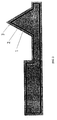
- FIG. 1 One possible embodiment of the arrangement according to the invention is schematically illustrated in FIG. 1. It consists of the following main elements:
- the measurement tip ( 1 ) which serves to map the surface topography consists of Si 3 N 4 , yet with the present method it may be produced of any material.
- the height and shape of the measurement tip can be varied. Typical dimensions, without restriction of the generality, are a height of 0.2 ⁇ m at a radius of curvature of the tips of ⁇ 30 nm.
- the geometry of the ultramicroelectrode may be varied controlledly in terms of shape and size.
- the distance of the electrode to the sample surface is adjusted by the height of the above-described measurement tip (i).
- Size and geometry (circular, elliptical, rectangular and also irregular electrode areas) of the electrically active area of the ultramicroelectrode can be produced and varied in controlled manner, just like the distance of the ultramicroelectrode from the surface and the relation of this distance to the electrically active area of the ultramicroelectrode.
- the jacket of the device produced according to the invention is electrically insulating and chemically inert relative to the solutions used during measurement in liquid media.
- FIG. 1 shows a principle outline of the measurement device according to the invention in a) schematic cross-section and b) schematic perspective view;
- FIG. 2 shows a principle outline to describe the production method according to the invention
- FIG. 3 shows a principle outline to describe the production method according to the invention, a) view of a side face, and b) view of an end face;
- FIG. 4 shows a principle outline of the measurement device according to the invention
- FIG. 5 shows a principle outline to describe the production method according to the invention
- FIG. 6 shows a principle outline to describe the production method according to the invention for multielectrodes.
- FIG. 7 shows a principle outline to describe the production method according to the invention for multielectrodes comprising an electrically conductive measurement tip.
- the device according to the invention can advantageously be produced with a method according to the invention as will be described in more detail in the following.
- the production method illustrated in the attached principle outlines (FIGS. 2 to 5 ) substantially comprises the following steps:
- a base body at first in the form of an Si 3 N 4 cantilever (FIG. 2( 1 )).
- a conductive layer is applied, in the exemplary embodiment 200 nm of gold are sputtered thereon.
- the electrically conductive layer is covered with an insulating layer which must be resistant to the solutions used during measurements in liquid media (FIG. 2( 3 )).
- a silicon nitride layer having a thickness of 900 nm has been deposited e.g. by means of a plasma-supported CVD process.
- the outer insulating layer covering the electrode and a part of the electrode and of the base body is locally removed (regions indicated in broken lines in FIG. 3) by means of a material-removing method, preferably with a focussed ion beam arrangement, as illustrated in FIG. 3.
- This process is carried out once, from the side face (FIG. 3 a ) and once, offset by 90° thereto, from the end face (FIG. 3 b ).
- a new measurement tip is formed, preferably by means of the focussed ion beam device as in the previous method step, by removing the regions indicated in broken lines in FIG. 4, once from the side face and once from the end face.
- the measurement tip may be formed by a suitable selection of the material removal from the material of the base body (FIG. 4 a ), the conductive layer (FIG. 4 b ) or the insulating layer covering the metal (FIG. 4 c ). Illustrations d, e and f in FIG. 4 show the resultant tip configurations.
- the height of the tip, the radius of the tip and the shape of the tip can also be varied by a suitable selection of the material removal.
- the measurement tip consists of the material of the cantilever used.
- the electrode areas in the exemplary embodiment are cleaned by a special form of material removal from re-deposited material with the FIB (single pass mill).
- the material-removing ion beam scans the region indicated in FIG. 5 in broken lines just once, from top to bottom, so that finally the sample surface is sputtered by the ion beam just once and re-deposited material is removed thereby.
- any other method that cleans the surface while maintaining the structure such as, e.g., an etching process, may be used for cleaning the electrode areas.
- Contacting the ultramicroelectrode may take place at any point desired, by locally removing the uppermost insulating layer by a structuring method and baring a respective connecting contact to the conductive layer.
- contacting of the ultramicroelectrode is effected at the rear end of the glass body of the cantilever (FIG. 1).
- the electrically active area of the probe can be varied independently of the pedestal height entered in FIG. 3.
- the electrode areas can be diminished for greater pedestal heights (FIG. 3).
- the geometry of the electrode can be varied by the choice of the base body on which the electrically conductive layer is applied.
- a cantilever was used with whose pyramid-shaped tip a suqare frame electrode results—as is apparent from FIG. 1.
- a base body of any desired shape may be used as the starting material, and thus, e.g., circular, elliptic, rectangular or polygonal electrodes can be realized.
- any desired—also irregular—shape of the base body can be provided, whereby it becomes possible to realize non-closed, in particular also segmented, ultramicroelectrodes.
- the ratio electrode area/distance of the electrode to the sample surface can be varied by adjusting the height of the measurement tip.
- the lateral distance of the microelectrode from the measurement tip for determining the surface topology may, as in the exemplary embodiment, be determined by the pedestal height (FIG. 3), with the base body having an appropriate shape.
- the method according to the invention is not limited.
- an alternating coating of the insulating base body with conductive and insulating layers and, analogous to the exemplary embodiment subsequent local removal of the material, thus also multielectrodes can be produced.
- the distances of the individual electrodes to the sample surface may vary.
- FIG. 6 shows an exemplary embodiment for a double electrode.
- the method described will apply with the modification that the material-removing step can be carried out twice with different pedestal heights (FIG. 6).
- the production of the measurement tip proper and the removal of redeposited material from the electrode is carried out analogously to the above-described exemplary embodiment.
- any desired multilayer systems can be built up and thus, multielectrodes can be realized.
- any material may be used as the base body of the probe, in particular also fibre-optic guides and, generally, wave guides for electromagnetic waves.
- a light beam generally electromagnetic waves
- an external jacket layer may in this way be used as a wave guide or as a fiber-optic wave guide.
Abstract
Description
- The present invention relates to a method of producing a device for simultaneously carrying out an electrochemical and a topographical near field microscopy.
- The utilization of ultramicroprobes for the laterally resolved characterization of sample surfaces provides quantitative and semi-quantitative data on the size as well as surface activity/surface reactivity, on the kinetics of heterogeneous as well as homogeneous electro-transfer reactions, on corrosion processes, on the activity of biological components and systems (e.g. the quantitation of enzyme activities, the examination of substance transport phenomena on membranes, tissues and tissue parts, metabolic activities of individual cells, cell groups and cell clusters, as well as organ parts and organs), and can also be applied to the large field of the laterally resolved surface modification by means of etching (removal of material) or deposition (application of material).
- A prerequisite for this is, however, an exact, reproducible control of the distance between the probe and the sample surface in the range of a few electrode radii. To date, in most of the applications described in the literature, the change in the Faraday current in the near field range, measured at the electrode, has been used for positioning (cf. Bard et al., Science 254 (1991), 68-74).
- Since, however, just as previously, in the real experiment, it can be departed neither from an ideal electrode geometry (particularly when the electrodes become very small), nor from an ideally parallel arrangement of the electrode to the sample surface, only a relative determination of the distance between the ultramicroelectrode and the surface is possible.
- Since in the conventional experiment the ultramicroelectrode does not only follow the topographical realities, the image obtained of the surface represents an overlaying of the influences of the electrochemical activity and the distance between the sample surface and the probe on the measured Faraday current at the ultramicroelectrode. These overlaying influences increase proportionally to the decrease in the electroactive probe area.
- Since a marked improvement in the resolution can only be obtained by using smaller electrodes (<1 μm radius), an alternative distance control must be used.
- First approaches to solve this problem are based on a vertical modulation of the electrode, on the one hand, so as to allow for a differentiation between conductive regions with a current increase and non-conductive regions with a current decrease (cf. Wipf et al., Anal. Chem. 64 (1992), 1362-1367). By a logic circuit, the microelectrode can be guided to follow the topography, yet not in the border regions between conductive and non-conductive. On the other hand, the distance control is based on convective effects which, if the probe is quickly moved perpendicularly towards the surface; will lead to changes in the current (cf. Borgwarth et al., Ber. Bunsenges. Phys. Chem. 98 (1994), 1317).
- Both methods are furthermore based on a current-dependent signal, and the distance between probe and sample cannot be exactly determined from the approximate curves.
- On the other hand, a current-independent height control based on the detection of shearing forces, as has already been used in the scanning near field optical microscopy, could be successfully used for the positioning of microelectrodes. (Ludwig et al., Rev. Sci. Instr. 66 (1995), 2857-2860). The basis of the shearing-force-based height control is the stimulation of the microelectrode to oscillations horizontally to the surface by means of a piezo-element, and the detection of the oscillation damping due to hydrodynamic effects if the probe is made to approach the sample surface.
- In U.S. Pat. No. 5,936,237, a combination of electromagnetic and topographical near field microscopy is described. An electrochemical near field microscopy is, however—simply due to the completely different local interactions on which it is based and the structural measures involved for the electrochemical measurement, on the one hand, and the electromagnetic measurement, on the other hand—not possible with the device described therein.
- Ludwig et al. describe a current-independent height control based on an optical detection principle. A laser beam focussed on the tip of the probe produces a Fresnel diffraction pattern which is detected at a divided photodiode and amplified by means of a lock-in technique.
- Apart from the optical method, also mechanical methods based on a small tuning fork of piezo-electrical material which is fastened on the microelectrode can be utilized for detection of the oscillation (James et al., J. Electrochem. Soc., 145 (1998), L64-L66). In this approach, the oscillation amplitude at the tip of the probe must be chosen to be so small that the electrochemical signal will not be substantially falsified. This precondition simultaneously constitutes the substantial limit for the use of ultramicroelectrodes and, thus, for an improved lateral resolution.
- A further approach for an independent topographical recording has been described by Macpherson et al. (Macpherson et al., Anal. Chem., 72 (2000), 276). This is based on the production of microelectrodes whose geometry and properties are adapted to an AFM cantilever. For this purpose, a fine tip is shaped on a platinum wire on one side thereof by etching, and the portion of the wire located therebehind is compressed to be flat. By bending the tip by 90°, an electrode similar to the cantilever is formed which is insulated by means of an electric deposition lacquer, except for the electrode tip.
- Due to its elasticity, the flattened portion serves for a distance control, based on the force interaction between sample and probe in the near field region.
- With such tips and with the assistance of an AFM device, it has been possible to form sample surfaces, e.g. ultrafiltration membranes, in contact mode. With the approach described, electrodes having a variation width of the electro-active area in the μm and sub-μm-range could be produced, in which, simplified, a hemispheric geometry was assumed and the electro-active area was estimated with the assistance of cyclical voltametry.
- However, the essential limits are to be seen both in the type of sample to be examined and in the little reproducible production of the electrochemical probes by the etching and insulating process, as well as in the poor topographical resolution due to the undefined tip geometry, as has been demonstrated by way of the quality of the recorded AFM images with decreasing tip size.
- For a significant improvement in the resolution ability for a laterally resolved, electro-chemical characterisation of surfaces, the electrically active area of the microprobe must be diminished, and the positioning of the electrode absolute to the surface must occur completely independent of any current. This, however, requires a de-coupling of the distance information and the electrochemical signal as a precondition. The topographical information should be ensured with as high a resolution as possible.
- It is an object of the present invention to provide a device which allows for a simultaneous, yet mutually decoupled, direct determination of topology and electrochemical activity. The shape of the device or of the ultramicroelectrode integrated therein or combined therewith, the electrically active area and the ratio of electrode area to the distance to the surface shall be variable. In particular, a method of producing such device is to be provided which is highly reproducible, allows for a simple serial production and an optimum measurement performance.
- According to the invention, this object is achieved by a method of producing a device for simultaneously carrying out electrochemical and a topological near field microscopy, wherein a probe suitable for topological imaging by near field technology is covered by a conductive material, the conductive material is covered by an insulating layer, and the conductive material and the insulating layer are removed in the region of the immediate tip of the probe. With the present method not only a suitable device can be provided which allows for electrochemical examinations of surfaces with a simultaneous determination of the surface topology, but according to the invention the highly reproducible production of this measuring device is enabled by an amazingly simple method. The method according to the invention can also be easily included in already existing manufacturing processes, since, e.g., conventional topological near field probes can be used as the starting material. By the method according to the invention it is ensured that the region for the electrochemical near field measurement of the device which is defined by the conductive material which is capable of receiving the signals obtained from the sample surface after the insulating layer has been removed, does not extend as far as to the outermost tip of the device, but starts at a defined distance from the immediate tip of the device (on which the interaction for the topological examination of the surface takes place). In this manner, not only the danger of a contact of the electrochemical near field measurement device with the surface is prevented, but also a negative influence on the topological near field measurement.
- General illustrations of various techniques applicable within the scope of the present invention for topographical and electrochemical near field microscopy (scanning probe microscopy) can be found in Bottomley (Anal. Chem. 70 (1998), 425R-475R) and in Wiesendanger (Scanning Probe Microscopy and Spectroscopy (Methods and Application) (Ed. R. Wiesendanger), Cambridge Press (1994)), which are included herewith as disclosure.
- What is essential to the method according to the invention is that, starting from a probe suitable for topological near field measurement, by applying and insulating a conductive material, the electrochemical near field measurement can be combined with the topological near field measurement in a simple manner. By removing conductive material and insulating layer in the region of the immediate tip of the device, not only the functioning ability of the (probe) tip required for the topological near field measurement is restored again, but also a region is created with which the conductive material is made accessible again for measuring surface effects in the electrochemical near field. The insulating layer applied over the conductive material has the effect that the signals will only enter via regions which have deliberately been bared again.
- Thus, it is essential that the region for electrochemical near field microscopy is created by covering the device for topographical near field measurement (“tip”, “cantilever”) with a conductive material. Such covering may be complete (“envelope”), yet it is also possible to cover merely certain areas of the device for topographical near field measurement (e.g. in the form of conductive tracks along the longitudinal axis of the cantilever) with a conductive material.
- In case that the device for topographical near field measurement itself is conductive (e.g. in the scanning tunneling microscope tip; “scanning tunneling microscopy” (STM); or in scanning near field optical microscopy (SNOM) tips)), this conductive device itself must, of course at first be insulated in the device according to the invention, and on this insulating layer, the conductive material for the electrochemical near field measurement must be present. In this instance, the insulated form of the device for topographical near field measurement is (at least partially) covered with the conductive material so as to provide the device for electrochemical near field measurement which, in turn, then must also be insulated (with the exception of the measurement region).
- This insulation of the device according to the invention is essential since the electrochemical near field measurement always must be performed in a liquid medium (electrolyte; liquid, conductive phase), and accordingly those parts of the device for the electrochemical near field measurement which do not serve for the immediate measurement (“measurement area”) must be protected against the liquid medium present during the measurement, which medium, as a rule, covers the surface to be measured, so as to avoid any undesired influences on this measurement.
- The manner in which the topological near field probe is covered with the conductive material is not critical. In general, for reasons of process technology, it will be preferred for the topological near field probe to be enveloped with the conductive material. It is, however, also possible to provide, e.g., merely one side of the probe with the conductive material. What is essential is only that the conductive layer is supplied from the region in which the electrochemical near field interaction with the surface is to be measured, to a suitable site of contact in another region of the electrode, from which site the measurement signal can be taken.
- The preferred conductive materials are either metals or they contain a metallic component, in particular a transition metal, the use of gold, silver, platinum, palladium, tungsten, cadmium, aluminum, rhodium, iridium, copper, mercury alloys, a platinum-iridium-alloy, a platinum-rhodium-alloy, carbon, carbon electrode-glassy carbon, high-order pyrolytic graphite (HOPG) being particularly preferred. Furthermore, also materials, such as polysilicon, e.g., doped, metal nitrides (TiN, TaN, . . . ) or all silicides (tungsten silicide, tantalum silicide, . . . ) may be considered as preferred materials.
- The manner in which the probe suited for topological near field measurement is covered with the conductive material is not critical and will depend on the respective material to be applied. Particularly suitable methods comprise ion sputtering, electron sputtering, chemical vapor deposition (CVD), electroless plating, electroplating and so on, in individual cases, however, also liquid phase deposition processes and spincoating methods may, advantageously, be used.
- The covering of the layer of conductive material with the insulating layer preferably is effected by deposition from the gas phase, by a CVD process, in particular, however, also by a plasma-supported CVD process, ion sputtering, electron sputtering, electroless plating, electroplating and application of insulating polymer layers, yet in individual cases also liquid phase deposition processes and spincoating methods are conceivable. With the insulation it must be ensured that the conductive material is completely covered so that the conductive material (except for the measurement region bared later on) does not have any contact to the electroactive medium.
- The baring of a certain region of the conductive layer is effected by the intentional removal of the insulating layer and the layer of conductive material. The removal of the conductive material and/or the removal of the insulating layer preferably are effected by a focussed ion beam, optionally a neutral particle beam, by an etching process, by laser or by focussed electromagnetic waves, removal by focussed ion beam being particularly preferred (cf. e.g. Matsui et al., Nanotechnology 7 (1996), 247-258).
- According to the invention, the inventive device may also be equipped with further layers or with different layer sequences, and be provided with a modified electrode which is designed as a microbiosensor, such as, e.g., as enzyme electrode, pH sensitive ultramicroelectrode, potentiometric or amperometric ultramicroelectrode, ion-sensitive ultramicroelectrode, ionselective ultramicroelectrode, polymermodified ultramicroelectrode, biomimetic ultramicroelelctrode. The number and arrangement of the various regions for the electrochemical near field measurement in such a multielectrode and multisensor configuration accordingly can be increased deliberately, by varying this layer sequence and the number of layers so as to enable multiparameter measurements, such as, e.g., simultaneous, electrochemical, topographical and pH mapping.
- Furthermore, also several tips may be provided for topographical near field measurement, or several combination device according to the invention may be provided for topographical and for electrochemical near field measurement in one and the same device, respectively.
- A preferred variant of the method according to the invention thus relates to a method in which a conductive material is once more applied to the insulating layer which conductive material is covered by an insulating layer, and this application of conductive material and covering with an insulating layer optionally is repeated further times before the various conductive layers are bared again in the measurement region.
- The probe usable for the topological near field measurement as the base body of the inventive ultramicroelectrode preferably is a probe made of metal, of an insulator, of a semiconductor, of a fiber-optic light guide or of a wave guide. If the probe is an electric conductor, it must first be provided with an insulating layer, whereupon the method according to the invention can be carried out.
- Dimensioning of the layers (by which substantially the region is defined, in which the electrochemical near field effects are measured) will depend on the respective field of use and/or the resolution ability of the inventive device; accordingly, preferably the conductive material will be applied to have a thickness of from 10 to 2000 nm, preferably from 100 to 800 nm, in particular from 150 to 500 nm. What is also conceivable is a monoatomic or monomolecular conductive layer.
- Preferably, the insulating layer will be applied to have a thickness of from 50 to 5000 nm, preferably from 100 to 2000 nm, in particular from 500 to 1500 nm. Here, too, however, also monoatomic or monomolecular layers are conceivable.
- The region in which the conductive material and the insulating layer are removed will also depend on the planned field of application of the device according to the invention and its measurement characteristics, respectively, and will also depend on the respective method of removing these layers. Preferably, a region from the immediate tip as far as to a distance from the immediate tip of from 10 to 2000 nm, preferably from 50 to 1000 nm, in particular from 100 to 500 nm is removed, wherein in each individual case the particular geometry of the probe, forming the basis from which it is started out with, must be taken into consideration.
- Preferably, it is already provided in the inventive production method itself that suitable connecting devices are provided at the device for recording the measurement signals.
- In a further aspect, the present invention relates to a device which can be obtained according to the present method.
- Thus, with the device according to the invention, both the electrochemical examination of surfaces and also the determination of the surface topology is possible simultaneously and with high resolution at the same site.
- One possible embodiment of the arrangement according to the invention is schematically illustrated in FIG. 1. It consists of the following main elements:
- (i) an insulated measurement tip ( 1) for topology examination;
- (ii) an ultramicroelectrode ( 2) surrounding the measurement tip;
- (iii) an insulated jacket ( 3) which electrically insulates the measurement probe with the exception of the measurement tip, the ultramicroelectrode and the connection area;
- (iv) a connecting face ( 4) electrically conductively connected with the ultramicroelectrode.
- In the measurement tip according to the invention, the measurement tip ( 1) which serves to map the surface topography consists of Si3N4, yet with the present method it may be produced of any material. The height and shape of the measurement tip can be varied. Typical dimensions, without restriction of the generality, are a height of 0.2 μm at a radius of curvature of the tips of <30 nm.
- The geometry of the ultramicroelectrode may be varied controlledly in terms of shape and size. The distance of the electrode to the sample surface is adjusted by the height of the above-described measurement tip (i).
- An insulating cover layer (iii), e.g. of, silicon nitride, covers the entire probe with the exception of the ultramicroelectrode, the connecting area and the measurement tip, and with the measurement tip according to the invention it is, e.g., a nitride layer having a thickness of 900 nm, which preferably is applied by means of CVD. Yet, also any other insulating layer which meets the requirements in terms of insulation, flexibility and resistance relative to the media used in the measurement is possible. This insulating layer must be sufficiently thick so as to guarantee an insulation, and sufficiently thin so as not to restrict the dynamic properties of the measurement tip.
- Size and geometry (circular, elliptical, rectangular and also irregular electrode areas) of the electrically active area of the ultramicroelectrode can be produced and varied in controlled manner, just like the distance of the ultramicroelectrode from the surface and the relation of this distance to the electrically active area of the ultramicroelectrode.
- The jacket of the device produced according to the invention is electrically insulating and chemically inert relative to the solutions used during measurement in liquid media.
- The invention will be explained in more detail by way of the following exemplary embodiments as well as the drawing figures to which, however, it is not restricted.
- Therein,
- FIG. 1 shows a principle outline of the measurement device according to the invention in a) schematic cross-section and b) schematic perspective view;
- FIG. 2 shows a principle outline to describe the production method according to the invention;
- FIG. 3 shows a principle outline to describe the production method according to the invention, a) view of a side face, and b) view of an end face;
- FIG. 4 shows a principle outline of the measurement device according to the invention;
- FIG. 5 shows a principle outline to describe the production method according to the invention;
- FIG. 6 shows a principle outline to describe the production method according to the invention for multielectrodes; and
- FIG. 7 shows a principle outline to describe the production method according to the invention for multielectrodes comprising an electrically conductive measurement tip.
- The device according to the invention can advantageously be produced with a method according to the invention as will be described in more detail in the following. The production method illustrated in the attached principle outlines (FIGS. 2 to 5) substantially comprises the following steps:
- In a device according to the invention with an integrated ultramicroelectrode, in the examplary embodiment there is a base body at first in the form of an Si 3N4 cantilever (FIG. 2(1)). Onto the latter, a conductive layer is applied, in the exemplary embodiment 200 nm of gold are sputtered thereon. The electrically conductive layer is covered with an insulating layer which must be resistant to the solutions used during measurements in liquid media (FIG. 2(3)). In the measurement device according to the invention, e.g. a silicon nitride layer having a thickness of 900 nm has been deposited e.g. by means of a plasma-supported CVD process.
- In the next step, the outer insulating layer covering the electrode and a part of the electrode and of the base body is locally removed (regions indicated in broken lines in FIG. 3) by means of a material-removing method, preferably with a focussed ion beam arrangement, as illustrated in FIG. 3. This process is carried out once, from the side face (FIG. 3 a) and once, offset by 90° thereto, from the end face (FIG. 3b).
- From the remaining cuboid with the pyramid put thereupon and having the material sequence insulator-metal-insulator, a new measurement tip is formed, preferably by means of the focussed ion beam device as in the previous method step, by removing the regions indicated in broken lines in FIG. 4, once from the side face and once from the end face.
- According to the invention, the measurement tip may be formed by a suitable selection of the material removal from the material of the base body (FIG. 4 a), the conductive layer (FIG. 4b) or the insulating layer covering the metal (FIG. 4c). Illustrations d, e and f in FIG. 4 show the resultant tip configurations.
- The height of the tip, the radius of the tip and the shape of the tip can also be varied by a suitable selection of the material removal. In the exemplary embodiment, the measurement tip consists of the material of the cantilever used.
- Finally, the electrode areas in the exemplary embodiment are cleaned by a special form of material removal from re-deposited material with the FIB (single pass mill). In this single pass mill, the material-removing ion beam scans the region indicated in FIG. 5 in broken lines just once, from top to bottom, so that finally the sample surface is sputtered by the ion beam just once and re-deposited material is removed thereby.
- According to the invention, however, any other method that cleans the surface while maintaining the structure, such as, e.g., an etching process, may be used for cleaning the electrode areas.
- Contacting the ultramicroelectrode may take place at any point desired, by locally removing the uppermost insulating layer by a structuring method and baring a respective connecting contact to the conductive layer.
- In the above exemplary embodiment, contacting of the ultramicroelectrode is effected at the rear end of the glass body of the cantilever (FIG. 1).
- From the method according to the invention, there result, e.g., the following possibilities of varying the electrode area or geometry, or the ratio of electrode area to the distance of the electrode from the sample surface and the lateral distance of the electrode (of the region for the electrochemical near field measurement) from the measurement tip (the region for topological near field measurement):
- 1. By applying electrically conductive layers of different thicknesses, the electrically active area of the probe can be varied independently of the pedestal height entered in FIG. 3.
- 2. With a fixed thickness of the electrically conductive layer, as is the case in the exemplary embodiment, with a pyramid-shaped base body, the electrode areas can be diminished for greater pedestal heights (FIG. 3).
- 3. The geometry of the electrode can be varied by the choice of the base body on which the electrically conductive layer is applied. In the exemplary embodiment, a cantilever was used with whose pyramid-shaped tip a suqare frame electrode results—as is apparent from FIG. 1. According to the invention, however, a base body of any desired shape may be used as the starting material, and thus, e.g., circular, elliptic, rectangular or polygonal electrodes can be realized. With the focussed ion beam device used in the exemplary embodiment, just as in any suitable structuring method, any desired—also irregular—shape of the base body can be provided, whereby it becomes possible to realize non-closed, in particular also segmented, ultramicroelectrodes.
- 4. The ratio electrode area/distance of the electrode to the sample surface can be varied by adjusting the height of the measurement tip.
- 5. The lateral distance of the microelectrode from the measurement tip for determining the surface topology may, as in the exemplary embodiment, be determined by the pedestal height (FIG. 3), with the base body having an appropriate shape.
- In terms of number of layers and sequence of layers, the method according to the invention is not limited. By an alternating coating of the insulating base body with conductive and insulating layers and, analogous to the exemplary embodiment, subsequent local removal of the material, thus also multielectrodes can be produced. The distances of the individual electrodes to the sample surface may vary. As an example, FIG. 6 shows an exemplary embodiment for a double electrode. For a probe according to the invention comprising several integrated electrodes, the method described will apply with the modification that the material-removing step can be carried out twice with different pedestal heights (FIG. 6). The production of the measurement tip proper and the removal of redeposited material from the electrode is carried out analogously to the above-described exemplary embodiment.
- If an electrically conductive material is used as the base body, a double electrode will be obtained by a series of structuring depositing and etching steps, with the measurement tip itself now being electrically conductive (FIG. 7).
- In this case, any desired multilayer systems can be built up and thus, multielectrodes can be realized.
- Any material may be used as the base body of the probe, in particular also fibre-optic guides and, generally, wave guides for electromagnetic waves. In this instance, e.g., a light beam (general electromagnetic waves) can be guided as far as to the probe tip and onto the sample. Moreover, also an external jacket layer may in this way be used as a wave guide or as a fiber-optic wave guide.
Claims (14)
Applications Claiming Priority (3)
| Application Number | Priority Date | Filing Date | Title |
|---|---|---|---|
| AT1011/2000 | 2000-06-09 | ||
| AT0101100A AT410032B (en) | 2000-06-09 | 2000-06-09 | METHOD FOR PRODUCING A DEVICE FOR SIMULTANEOUSLY IMPLEMENTING AN ELECTROCHEMICAL AND A TOPOGRAPHIC NEAR FIELD MICROSCOPY |
| PCT/AT2001/000191 WO2001094926A1 (en) | 2000-06-09 | 2001-06-11 | Method for producing a device for simultaneously carrying out an electrochemical and a topographical near-field microscopy |
Publications (2)
| Publication Number | Publication Date |
|---|---|
| US20030190425A1 true US20030190425A1 (en) | 2003-10-09 |
| US7074340B2 US7074340B2 (en) | 2006-07-11 |
Family
ID=3684056
Family Applications (1)
| Application Number | Title | Priority Date | Filing Date |
|---|---|---|---|
| US10/297,562 Expired - Lifetime US7074340B2 (en) | 2000-06-09 | 2001-06-11 | Method for producing a device for simultaneously carrying out an electrochemical and a topographical near-field microscopy |
Country Status (6)
| Country | Link |
|---|---|
| US (1) | US7074340B2 (en) |
| EP (1) | EP1290431B1 (en) |
| AT (2) | AT410032B (en) |
| AU (1) | AU2001267123A1 (en) |
| DE (1) | DE50113864D1 (en) |
| WO (1) | WO2001094926A1 (en) |
Cited By (7)
| Publication number | Priority date | Publication date | Assignee | Title |
|---|---|---|---|---|
| US20030230709A1 (en) * | 2002-06-14 | 2003-12-18 | Canon Kabushiki Kaisha | Probe, near-field light generation apparatus including probe, exposure apparatus, and exposing method using probe |
| US20100115673A1 (en) * | 2006-11-27 | 2010-05-06 | Christine Kranz | Near field scanning measurement-alternating current-scanning electrochemical microscopy devices and mehtods of use thereof |
| US20120027928A1 (en) * | 2007-09-27 | 2012-02-02 | Infineon Technologies Ag | Electronic device |
| US20130032495A1 (en) * | 2010-04-16 | 2013-02-07 | Patrick Unwin | Scanning electrochemical microscopy |
| CN111591953A (en) * | 2020-05-07 | 2020-08-28 | 南京航空航天大学 | Needle-shaped microelectrode and preparation method thereof |
| CN112067853A (en) * | 2020-08-28 | 2020-12-11 | 中国科学院城市环境研究所 | Microorganism modification scanning photoelectrochemical microscope system and imaging method thereof |
| US20210050381A1 (en) * | 2019-08-15 | 2021-02-18 | Ultra Display Technology Corp. | Electronic detection interface and electronic detection module using the same |
Families Citing this family (23)
| Publication number | Priority date | Publication date | Assignee | Title |
|---|---|---|---|---|
| DE102004012520A1 (en) * | 2004-03-05 | 2005-09-29 | Leibniz-Institut Für Festkörper- Und Werkstoffforschung Dresden E.V. | Point source for electron field emissions with local shielding |
| GB0412844D0 (en) * | 2004-06-09 | 2004-07-14 | Univ Warwick | Probe |
| KR100707204B1 (en) * | 2005-08-16 | 2007-04-13 | 삼성전자주식회사 | Semiconductor probe with resistive tip of low aspect ratio and method of fabricating the same |
| DE102006004922B4 (en) | 2006-02-01 | 2008-04-30 | Nanoscale Systems Nanoss Gmbh | Miniaturized spring element and method for its production, beam probe, atomic force microscope and method for its operation |
| WO2008091371A2 (en) | 2006-07-18 | 2008-07-31 | Multiprobe, Inc. | Apparatus and method for combined micro-scale and nano-scale c-v,q-v, and i-v testing of semiconductor materials |
| US7869334B2 (en) * | 2007-03-19 | 2011-01-11 | Intel Corporation | Seek-scan probe (SSP) memory with sharp probe tips formed at CMOS-compatible temperatures |
| US7928343B2 (en) * | 2007-12-04 | 2011-04-19 | The Board Of Trustees Of The University Of Illinois | Microcantilever heater-thermometer with integrated temperature-compensated strain sensor |
| US8719960B2 (en) * | 2008-01-31 | 2014-05-06 | The Board Of Trustees Of The University Of Illinois | Temperature-dependent nanoscale contact potential measurement technique and device |
| US8931950B2 (en) | 2008-08-20 | 2015-01-13 | The Board Of Trustees Of The University Of Illinois | Device for calorimetric measurement |
| US8955161B2 (en) | 2008-11-13 | 2015-02-10 | Bruker Nano, Inc. | Peakforce photothermal-based detection of IR nanoabsorption |
| WO2010057052A2 (en) * | 2008-11-13 | 2010-05-20 | Veeco Instruments Inc. | Method and apparatus of operating a scanning probe microscope |
| US8650660B2 (en) | 2008-11-13 | 2014-02-11 | Bruker Nano, Inc. | Method and apparatus of using peak force tapping mode to measure physical properties of a sample |
| US8387443B2 (en) | 2009-09-11 | 2013-03-05 | The Board Of Trustees Of The University Of Illinois | Microcantilever with reduced second harmonic while in contact with a surface and nano scale infrared spectrometer |
| KR101852475B1 (en) | 2009-12-01 | 2018-06-11 | 브루커 나노, 인코퍼레이션. | Method and apparatus of operating a scanning probe microscope |
| US20110304554A1 (en) * | 2010-06-10 | 2011-12-15 | Research In Motion Limited | Keypad stiffener and method of manufacture |
| US8726410B2 (en) | 2010-07-30 | 2014-05-13 | The United States Of America As Represented By The Secretary Of The Air Force | Atomic force microscopy system and method for nanoscale measurement |
| US8307461B2 (en) * | 2011-01-20 | 2012-11-06 | Primenano, Inc. | Fabrication of a microcantilever microwave probe |
| US8914911B2 (en) | 2011-08-15 | 2014-12-16 | The Board Of Trustees Of The University Of Illinois | Magnetic actuation and thermal cantilevers for temperature and frequency dependent atomic force microscopy |
| US8533861B2 (en) | 2011-08-15 | 2013-09-10 | The Board Of Trustees Of The University Of Illinois | Magnetic actuation and thermal cantilevers for temperature and frequency dependent atomic force microscopy |
| US10605827B2 (en) | 2015-12-14 | 2020-03-31 | Universidade Federal De Menas Gerais-Ufmg | Metallic device for scanning probe microscopy and method for manufacturing same |
| CN110168383A (en) | 2016-08-22 | 2019-08-23 | 布鲁克纳米公司 | Use the IR Characterization for the sample that peak force touches |
| CN112285505A (en) * | 2020-10-27 | 2021-01-29 | 国网重庆市电力公司电力科学研究院 | GIS detection imaging device based on laser focusing enhancement technology |
| EP4123314A1 (en) | 2021-07-21 | 2023-01-25 | Helmholtz-Zentrum Berlin für Materialien und Energie GmbH | Method for processing a probe for determining surface properties or modifying surface structures in the sub-micrometer area and probe |
Citations (8)
| Publication number | Priority date | Publication date | Assignee | Title |
|---|---|---|---|---|
| US593237A (en) * | 1897-11-09 | Electric switch for chandeliers or brackets | ||
| US5838005A (en) * | 1995-05-11 | 1998-11-17 | The Regents Of The University Of California | Use of focused ion and electron beams for fabricating a sensor on a probe tip used for scanning multiprobe microscopy and the like |
| US5936243A (en) * | 1997-06-09 | 1999-08-10 | Ian Hardcastle | Conductive micro-probe and memory device |
| US5965218A (en) * | 1997-03-18 | 1999-10-12 | Vlsi Technology, Inc. | Process for manufacturing ultra-sharp atomic force microscope (AFM) and scanning tunneling microscope (STM) tips |
| US5969238A (en) * | 1996-08-30 | 1999-10-19 | Max-Planck-Gesellschraft Zur Foerderung Der Wissenschaften E.V. | Thermoelectric microprobe |
| US6034348A (en) * | 1996-12-18 | 2000-03-07 | Electronics And Telecommunications Research Institute | Micro etching system using laser ablation |
| US6703614B1 (en) * | 1998-11-17 | 2004-03-09 | Carl Zeiss Jena Gmbh | Method for determining the distance of a near-field probe from a specimen surface to be examined, and near-field microscope |
| US6894272B2 (en) * | 2000-06-09 | 2005-05-17 | Innovationsagentur Gesellschaft Mbh | Device for simultaneously carrying out an electrochemical and a topographical near-field microscopy |
Family Cites Families (4)
| Publication number | Priority date | Publication date | Assignee | Title |
|---|---|---|---|---|
| EP0539731B1 (en) * | 1991-09-27 | 1997-01-02 | Matsushita Electric Industrial Co., Ltd. | Probe of scanning electrochemical microscope and method of manufacturing the same |
| US5844251A (en) * | 1994-01-05 | 1998-12-01 | Cornell Research Foundation, Inc. | High aspect ratio probes with self-aligned control electrodes |
| US5936237A (en) * | 1995-07-05 | 1999-08-10 | Van Der Weide; Daniel Warren | Combined topography and electromagnetic field scanning probe microscope |
| DE19636582C1 (en) * | 1996-09-09 | 1997-11-27 | Forschungszentrum Juelich Gmbh | Sensor for measuring ion concentrations |
-
2000
- 2000-06-09 AT AT0101100A patent/AT410032B/en not_active IP Right Cessation
-
2001
- 2001-06-11 EP EP01944719A patent/EP1290431B1/en not_active Expired - Lifetime
- 2001-06-11 DE DE50113864T patent/DE50113864D1/en not_active Expired - Lifetime
- 2001-06-11 WO PCT/AT2001/000191 patent/WO2001094926A1/en active IP Right Grant
- 2001-06-11 AU AU2001267123A patent/AU2001267123A1/en not_active Abandoned
- 2001-06-11 AT AT01944719T patent/ATE392700T1/en not_active IP Right Cessation
- 2001-06-11 US US10/297,562 patent/US7074340B2/en not_active Expired - Lifetime
Patent Citations (8)
| Publication number | Priority date | Publication date | Assignee | Title |
|---|---|---|---|---|
| US593237A (en) * | 1897-11-09 | Electric switch for chandeliers or brackets | ||
| US5838005A (en) * | 1995-05-11 | 1998-11-17 | The Regents Of The University Of California | Use of focused ion and electron beams for fabricating a sensor on a probe tip used for scanning multiprobe microscopy and the like |
| US5969238A (en) * | 1996-08-30 | 1999-10-19 | Max-Planck-Gesellschraft Zur Foerderung Der Wissenschaften E.V. | Thermoelectric microprobe |
| US6034348A (en) * | 1996-12-18 | 2000-03-07 | Electronics And Telecommunications Research Institute | Micro etching system using laser ablation |
| US5965218A (en) * | 1997-03-18 | 1999-10-12 | Vlsi Technology, Inc. | Process for manufacturing ultra-sharp atomic force microscope (AFM) and scanning tunneling microscope (STM) tips |
| US5936243A (en) * | 1997-06-09 | 1999-08-10 | Ian Hardcastle | Conductive micro-probe and memory device |
| US6703614B1 (en) * | 1998-11-17 | 2004-03-09 | Carl Zeiss Jena Gmbh | Method for determining the distance of a near-field probe from a specimen surface to be examined, and near-field microscope |
| US6894272B2 (en) * | 2000-06-09 | 2005-05-17 | Innovationsagentur Gesellschaft Mbh | Device for simultaneously carrying out an electrochemical and a topographical near-field microscopy |
Cited By (12)
| Publication number | Priority date | Publication date | Assignee | Title |
|---|---|---|---|---|
| US20030230709A1 (en) * | 2002-06-14 | 2003-12-18 | Canon Kabushiki Kaisha | Probe, near-field light generation apparatus including probe, exposure apparatus, and exposing method using probe |
| US7297933B2 (en) * | 2002-06-14 | 2007-11-20 | Canon Kabushiki Kaisha | Probe, near-field light generation apparatus including probe, exposure apparatus, and exposing method using probe |
| US20100115673A1 (en) * | 2006-11-27 | 2010-05-06 | Christine Kranz | Near field scanning measurement-alternating current-scanning electrochemical microscopy devices and mehtods of use thereof |
| US20120027928A1 (en) * | 2007-09-27 | 2012-02-02 | Infineon Technologies Ag | Electronic device |
| US8806741B2 (en) * | 2007-09-27 | 2014-08-19 | Infineon Technologies Ag | Method of making an electronic device |
| US20130032495A1 (en) * | 2010-04-16 | 2013-02-07 | Patrick Unwin | Scanning electrochemical microscopy |
| US20150059027A1 (en) * | 2010-04-16 | 2015-02-26 | University Of Warwick | Scanning electrochemical microscopy |
| US11921130B2 (en) | 2010-04-16 | 2024-03-05 | The University Of Warwick | Scanning electrochemical microscopy with oscillating probe tip |
| US20210050381A1 (en) * | 2019-08-15 | 2021-02-18 | Ultra Display Technology Corp. | Electronic detection interface and electronic detection module using the same |
| US11888011B2 (en) * | 2019-08-15 | 2024-01-30 | Ultra Display Technology Corp. | Electronic detection module for testing micro chips |
| CN111591953A (en) * | 2020-05-07 | 2020-08-28 | 南京航空航天大学 | Needle-shaped microelectrode and preparation method thereof |
| CN112067853A (en) * | 2020-08-28 | 2020-12-11 | 中国科学院城市环境研究所 | Microorganism modification scanning photoelectrochemical microscope system and imaging method thereof |
Also Published As
| Publication number | Publication date |
|---|---|
| US7074340B2 (en) | 2006-07-11 |
| AU2001267123A1 (en) | 2001-12-17 |
| DE50113864D1 (en) | 2008-05-29 |
| EP1290431B1 (en) | 2008-04-16 |
| ATE392700T1 (en) | 2008-05-15 |
| EP1290431A1 (en) | 2003-03-12 |
| ATA10112000A (en) | 2002-05-15 |
| AT410032B (en) | 2003-01-27 |
| WO2001094926A1 (en) | 2001-12-13 |
Similar Documents
| Publication | Publication Date | Title |
|---|---|---|
| US7074340B2 (en) | Method for producing a device for simultaneously carrying out an electrochemical and a topographical near-field microscopy | |
| US6894272B2 (en) | Device for simultaneously carrying out an electrochemical and a topographical near-field microscopy | |
| US7444856B2 (en) | Sensors for electrochemical, electrical or topographical analysis | |
| Pust et al. | Influence of electrode size and geometry on electrochemical experiments with combined SECM–SFM probes | |
| Kranz et al. | Integrating an ultramicroelectrode in an AFM cantilever: combined technology for enhanced information | |
| US6252226B1 (en) | Nanometer scale data storage device and associated positioning system | |
| WO1997004449A1 (en) | Nanometer scale data storage device and associated positioning system | |
| Salomo et al. | Integrated cantilever probes for SECM/AFM characterization of surfaces | |
| US20100115673A1 (en) | Near field scanning measurement-alternating current-scanning electrochemical microscopy devices and mehtods of use thereof | |
| KR20070075660A (en) | Conductive carbon nanotube tip, probe of scanning probe microscope comprising the same and manufacturing method of the conductive carbon nanotube tip | |
| US6245204B1 (en) | Vibrating tip conducting probe microscope | |
| Lugstein et al. | Fabrication of a ring nanoelectrode in an AFM tip: novel approach towards simultaneous electrochemical and topographical imaging | |
| JP4656761B2 (en) | SPM cantilever | |
| WO2012072507A1 (en) | AFM-SECM sensor | |
| KR101265776B1 (en) | Nano electrode and method for manutacturing of the same | |
| US6566650B1 (en) | Incorporation of dielectric layer onto SThM tips for direct thermal analysis | |
| US7156965B1 (en) | Scanning electrochemical potential microscope | |
| Baumeister et al. | Scanning Tunneling Microscopy II: Further Applications and Related Scanning Techniques | |
| Dobson et al. | Electron beam lithographically-defined scanning electrochemical-atomic force microscopy probes: fabrication method and application to high resolution imaging on heterogeneously active surfaces | |
| Moon et al. | Bitmap-assisted focused ion beam fabrication of combined atomic force scanning electrochemical microscopy probes | |
| JPH05288714A (en) | In-solution scanning tunneling microscope | |
| Lugstein et al. | FIB Based Micro Fabrication Technique for a Novel Type of Scanning Electrochemical Microscopy Probes | |
| Shin | Fabrication of atomic force microscope probes integrated with electrodes for micro four-point probe and SECM-AFM | |
| Smith et al. | Electrochemical SPM: Fundamentals and Applications | |
| Heintz et al. | Characterization of parylene coated combined scanning probe tips for in-situ electrochemical and topographical imaging |
Legal Events
| Date | Code | Title | Description |
|---|---|---|---|
| AS | Assignment |
Owner name: INNOVATIONSAGENTUR GESELLSCHAFT MBH, AUSTRIA Free format text: ASSIGNMENT OF ASSIGNORS INTEREST;ASSIGNORS:LUGSTEIN, ALOIS;BERTAGNOLLI, EMMERICH;KRANZ, CHRISTINE;AND OTHERS;REEL/FRAME:014088/0666;SIGNING DATES FROM 20030221 TO 20030319 Owner name: INNOVATIONSAGENTUR GESELLSCHAFT MBH, AUSTRIA Free format text: ASSIGNMENT OF ASSIGNORS INTEREST;ASSIGNORS:LUGSTEIN, ALOIS;BERTAGNOLLI, EMMERICH;KRANZ, CHRISTINE;AND OTHERS;REEL/FRAME:014054/0585;SIGNING DATES FROM 20030221 TO 20030319 |
|
| STCF | Information on status: patent grant |
Free format text: PATENTED CASE |
|
| FPAY | Fee payment |
Year of fee payment: 4 |
|
| FEPP | Fee payment procedure |
Free format text: PAT HOLDER NO LONGER CLAIMS SMALL ENTITY STATUS, ENTITY STATUS SET TO UNDISCOUNTED (ORIGINAL EVENT CODE: STOL); ENTITY STATUS OF PATENT OWNER: LARGE ENTITY |
|
| REFU | Refund |
Free format text: REFUND - PAYMENT OF MAINTENANCE FEE, 8TH YR, SMALL ENTITY (ORIGINAL EVENT CODE: R2552); ENTITY STATUS OF PATENT OWNER: LARGE ENTITY |
|
| FPAY | Fee payment |
Year of fee payment: 8 |
|
| MAFP | Maintenance fee payment |
Free format text: PAYMENT OF MAINTENANCE FEE, 12TH YEAR, LARGE ENTITY (ORIGINAL EVENT CODE: M1553) Year of fee payment: 12 |