US20030190419A1 - Method for forming a film, film forming device, liquid discharge device, method for manufacturing a color filter, display device having a color filter, method for manufacturing a display device, display device, and electronic apparatus - Google Patents
Method for forming a film, film forming device, liquid discharge device, method for manufacturing a color filter, display device having a color filter, method for manufacturing a display device, display device, and electronic apparatus Download PDFInfo
- Publication number
- US20030190419A1 US20030190419A1 US10/359,602 US35960203A US2003190419A1 US 20030190419 A1 US20030190419 A1 US 20030190419A1 US 35960203 A US35960203 A US 35960203A US 2003190419 A1 US2003190419 A1 US 2003190419A1
- Authority
- US
- United States
- Prior art keywords
- liquid discharge
- sweeping
- liquid
- droplets
- discharged
- Prior art date
- Legal status (The legal status is an assumption and is not a legal conclusion. Google has not performed a legal analysis and makes no representation as to the accuracy of the status listed.)
- Abandoned
Links
Images


Classifications
-
- E—FIXED CONSTRUCTIONS
- E04—BUILDING
- E04H—BUILDINGS OR LIKE STRUCTURES FOR PARTICULAR PURPOSES; SWIMMING OR SPLASH BATHS OR POOLS; MASTS; FENCING; TENTS OR CANOPIES, IN GENERAL
- E04H12/00—Towers; Masts or poles; Chimney stacks; Water-towers; Methods of erecting such structures
- E04H12/02—Structures made of specified materials
- E04H12/08—Structures made of specified materials of metal
- E04H12/10—Truss-like structures
-
- G—PHYSICS
- G02—OPTICS
- G02F—OPTICAL DEVICES OR ARRANGEMENTS FOR THE CONTROL OF LIGHT BY MODIFICATION OF THE OPTICAL PROPERTIES OF THE MEDIA OF THE ELEMENTS INVOLVED THEREIN; NON-LINEAR OPTICS; FREQUENCY-CHANGING OF LIGHT; OPTICAL LOGIC ELEMENTS; OPTICAL ANALOGUE/DIGITAL CONVERTERS
- G02F1/00—Devices or arrangements for the control of the intensity, colour, phase, polarisation or direction of light arriving from an independent light source, e.g. switching, gating or modulating; Non-linear optics
- G02F1/01—Devices or arrangements for the control of the intensity, colour, phase, polarisation or direction of light arriving from an independent light source, e.g. switching, gating or modulating; Non-linear optics for the control of the intensity, phase, polarisation or colour
- G02F1/13—Devices or arrangements for the control of the intensity, colour, phase, polarisation or direction of light arriving from an independent light source, e.g. switching, gating or modulating; Non-linear optics for the control of the intensity, phase, polarisation or colour based on liquid crystals, e.g. single liquid crystal display cells
- G02F1/133—Constructional arrangements; Operation of liquid crystal cells; Circuit arrangements
- G02F1/1333—Constructional arrangements; Manufacturing methods
- G02F1/1335—Structural association of cells with optical devices, e.g. polarisers or reflectors
- G02F1/133509—Filters, e.g. light shielding masks
- G02F1/133514—Colour filters
- G02F1/133516—Methods for their manufacture, e.g. printing, electro-deposition or photolithography
-
- B—PERFORMING OPERATIONS; TRANSPORTING
- B41—PRINTING; LINING MACHINES; TYPEWRITERS; STAMPS
- B41J—TYPEWRITERS; SELECTIVE PRINTING MECHANISMS, i.e. MECHANISMS PRINTING OTHERWISE THAN FROM A FORME; CORRECTION OF TYPOGRAPHICAL ERRORS
- B41J2/00—Typewriters or selective printing mechanisms characterised by the printing or marking process for which they are designed
- B41J2/005—Typewriters or selective printing mechanisms characterised by the printing or marking process for which they are designed characterised by bringing liquid or particles selectively into contact with a printing material
- B41J2/01—Ink jet
- B41J2/21—Ink jet for multi-colour printing
- B41J2/2107—Ink jet for multi-colour printing characterised by the ink properties
- B41J2/2114—Ejecting transparent or white coloured liquids, e.g. processing liquids
-
- F—MECHANICAL ENGINEERING; LIGHTING; HEATING; WEAPONS; BLASTING
- F21—LIGHTING
- F21S—NON-PORTABLE LIGHTING DEVICES; SYSTEMS THEREOF; VEHICLE LIGHTING DEVICES SPECIALLY ADAPTED FOR VEHICLE EXTERIORS
- F21S8/00—Lighting devices intended for fixed installation
- F21S8/08—Lighting devices intended for fixed installation with a standard
- F21S8/085—Lighting devices intended for fixed installation with a standard of high-built type, e.g. street light
-
- G—PHYSICS
- G02—OPTICS
- G02B—OPTICAL ELEMENTS, SYSTEMS OR APPARATUS
- G02B5/00—Optical elements other than lenses
- G02B5/20—Filters
- G02B5/201—Filters in the form of arrays
-
- H—ELECTRICITY
- H01—ELECTRIC ELEMENTS
- H01J—ELECTRIC DISCHARGE TUBES OR DISCHARGE LAMPS
- H01J9/00—Apparatus or processes specially adapted for the manufacture, installation, removal, maintenance of electric discharge tubes, discharge lamps, or parts thereof; Recovery of material from discharge tubes or lamps
- H01J9/20—Manufacture of screens on or from which an image or pattern is formed, picked up, converted or stored; Applying coatings to the vessel
-
- H—ELECTRICITY
- H05—ELECTRIC TECHNIQUES NOT OTHERWISE PROVIDED FOR
- H05K—PRINTED CIRCUITS; CASINGS OR CONSTRUCTIONAL DETAILS OF ELECTRIC APPARATUS; MANUFACTURE OF ASSEMBLAGES OF ELECTRICAL COMPONENTS
- H05K3/00—Apparatus or processes for manufacturing printed circuits
- H05K3/10—Apparatus or processes for manufacturing printed circuits in which conductive material is applied to the insulating support in such a manner as to form the desired conductive pattern
- H05K3/12—Apparatus or processes for manufacturing printed circuits in which conductive material is applied to the insulating support in such a manner as to form the desired conductive pattern using thick film techniques, e.g. printing techniques to apply the conductive material or similar techniques for applying conductive paste or ink patterns
- H05K3/1241—Apparatus or processes for manufacturing printed circuits in which conductive material is applied to the insulating support in such a manner as to form the desired conductive pattern using thick film techniques, e.g. printing techniques to apply the conductive material or similar techniques for applying conductive paste or ink patterns by ink-jet printing or drawing by dispensing
Definitions
- the present invention relates to a method for depositing a film, a device for depositing a film, a device for discharging droplets, a method for manufacturing a color filter, a display device including a color filter, a method for a manufacturing display device, a display device, and an electronic apparatus, and particularly to a technique for depositing a film by discharging droplets.
- EL devices liquid crystal display devices and electroluminescent display devices
- display means and electronic apparatuses having such a display device such as cellular phones and personal digital assistants
- the display devices Since it is becoming common that these display devices display color images, the display devices often include a color filter in which R (red), G (green), and B (blue) dots serving as filter elements are arrayed on the surface of a substrate formed of glass, resin, or the like in a predetermined arrangement, such as a striped arrangement, a delta arrangement, or a mosaic arrangement.
- display dots comprising R (red), G (green), and B (blue) dots serving as EL luminescent films disposed in a predetermined arrangement, such as a striped arrangement, a delta arrangement, a mosaic arrangement, or the like between pairs of electrodes are formed on a substrate of glass, resin, or the like.
- the display dots each emit light having predetermined color and gradation by controlling voltage applied to the electrodes from one display dot to another.
- the filter elements for colors of the color filter and the luminescent films for colors of the EL device are generally patterned by photolithography.
- a patterning step using photolithography requires complicated, time-consuming treatments, such as material deposition, exposure, and development.
- the patterning step undesirably consumes a large amount of color materials and resist, consequently increasing costs.
- filter elements 303 are arrayed by a ink jet technique, in a dot manner as shown in FIG. 61( b ), in a plurality of unit regions 302 on a so-called mother substrate 301 , which is a large-area substrate formed of glass, resin, or the like, as shown in FIG. 61( a ).
- These filter elements 303 are formed by arraying colors, such as R, G, and B, in a predetermined arrangement pattern, such as a striped arrangement, a delta arrangement, or a mosaic arrangement, as described above. Therefore, it is generally needed to use R, G, and B color ink jet heads 306 one by one in order to form a color filter in a predetermined color arrangement on the mother substrate 301 .
- the discharge quantity from the nozzles 304 constituting the nozzle line 305 generally varies.
- the ink jet head 306 has an ink discharge quality Q in that, for example, nozzles 304 at both ends of the nozzle line 305 offer the largest discharge quantity, nozzles 304 in the center of nozzle line 305 offer the larger discharge quantity, and the other nozzles 304 offer the smallest discharge quantity, as shown in FIG. 62( a ).
- the plurality of unit regions 302 are formed on the mother substrate 301 , different arrangement patterns (such as a striped arrangement, a delta arrangement, and a mosaic arrangement) are formed in the unit regions 302 in some cases so that the unit regions 302 correspond to the size or shape of the display of a resulting display device.
- the number of or the intervals between display dots having the same color in a certain direction on the mother substrate 301 are often varied from one model to another. If the ink jet head is swept over such a mother substrate 301 without variation, process efficiency is undesirably reduced. In this instance, ink jet heads having different structures may be prepared for respective models to increase process efficiency. However, the preparation of many ink jet heads increases costs.
- the present invention is intended to solve the above-described problems, and an object of the invention is to provide a technique for reducing the unevenness of film deposition in a method and a device for depositing films by discharging droplets with liquid discharge means. Another object of the present invention is to provide a device and a method for forming a film by discharging a liquid material with a liquid discharge head or the like, such as an ink jet head, and which can reduce the unevenness of film deposition resulting from variation of the quantity of the discharged liquid material. Still another object of the present invention is to provide a device and a method for forming a film by discharging a liquid material and which can increase process efficiency while suppressing the increase of costs, even if the liquid material is discharged onto various discharge objects.
- a method for forming a film by discharging a liquid material onto the surface of an object with a liquid discharge means comprises: a first sweeping step of discharging a plurality of droplets of the liquid material onto the surface of the object while the liquid discharge means sweeps over the object in a first direction with respect to the object, along the surface of the object; and a second sweeping step of discharging a plurality of droplets of the liquid material onto the surface while the liquid discharge means sweeps over the object in a second direction different from the first direction with respect to the object, along the surface of the object.
- the first direction and the second direction are selected by rotating the object to orient in a direction different from each other between the first movement step and the second movement step such that the first direction and the second direction intersect each other. Since the orientation of the object is changed, it is not necessary to change the sweeping direction of the liquid discharge means. Consequently, film deposition can be performed by a simple system, but not a large mechanism.
- the present invention provides a film forming device comprising: liquid discharge means for discharging droplets of a liquid material onto the surface of an object; and shifting means for relatively moving the object and the liquid discharge means, along the surface of the object.
- the liquid discharge means is relatively moved in at least two directions with respect to the object along the surface of the object, and the liquid discharge means discharges the droplets one after another while moving in any direction of said at least two directions.
- the sweeping direction can be selected from at least two directions, according to the film formation pattern which will be deposited onto an object.
- the film forming device further comprises an orientation means for orienting the object in at least two directions by rotating the object.
- the shifting means can become a simple structure in which the shifting means drives sweeping in only one direction.
- a miniaturized device and a reduced cost can be achieved on the whole.
- the present invention provides a liquid discharge device for discharging a liquid material onto an object.
- the liquid discharge device comprises a liquid discharge head for discharging the liquid material; shifting means for relatively moving the liquid discharge head and the object in a direction along the surface of the object, the liquid discharge head and the object opposing each other; and orientation means for horizontally orienting the object.
- the orientation means is capable of horizontally orienting the object in at least two different directions.
- the orientation means for horizontally orienting the object is capable of horizontally orienting the object in at least two different directions. Therefore, the sweeping direction of the liquid discharge head relative to the object can be selected from at least two directions according to the arrangement of the regions on the object in which droplets will be discharged. Thus, efficiency of discharge can be increased. Also, the sweeping direction of the liquid discharge head driven by the shifting means can be varied by changing the horizontal orientation of the object. As a result, by sweeping the liquid discharge head in two different directions to discharge droplets onto one object for depositing a film, striped unevenness of the material resulting from the sweeping direction can be reduced.
- the orientation means comprises a plurality of observing means for observing different portions of the object. Some of the observing means are used in one orientation relationship and the other observing means are used in the other orientation relationship.
- the observing means is capable of observing a plurality of portions of the object.
- the plurality of observing means can each observe the plurality of portions of the object, the horizontal orientation of the object can be precisely observed.
- the observing means capable of observing a plurality of portions of the object may include two imaging devices.
- the observing position by the observing means is fixed in the device.
- the two orientations are offered by rotating one horizontal orientation of the object about 90° on the normal of the surface of the object.
- the liquid discharge head can be swept in two directions perpendicular to each other, with respect to the object. Consequently, striped unevenness of the material resulting from the sweeping direction of the liquid discharge head with respect to the object can be reduced most effectively.
- the present invention provides a liquid discharge device for discharging a liquid material onto an object.
- the liquid discharge device comprises: a liquid discharge head for discharging the liquid material; shifting means for relatively moving the liquid discharge head and the object in a direction along the surface of the object, the liquid discharge head and the object opposing each other; and orientation means for horizontally orienting the object.
- the sweeping direction in which the liquid discharge head moves while discharging droplets of the liquid material onto the object and the orientation of the object oriented by the orientation means have at least two orientation relationships.
- the sweeping direction in which the liquid discharge head moves while discharging droplets of the liquid material onto the object and the orientation of the object oriented by the orientation means have at least two orientation relationships. Therefore, the sweeping direction of the liquid discharge head relative to the object can be selected from at least two directions according to the arrangement of the regions on the object in which droplets will be discharged. Thus, efficiency of discharge can be increased. Also, the sweeping direction of the liquid discharge head can be varied to two different directions with respect to the object. As a result, by sweeping the liquid discharge head in two different directions to discharge droplets onto one object, striped unevenness of the material resulting from the sweeping direction can be reduced.
- the orientation means comprises a plurality of observing means for observing different portions of the object. Some of the observing means are used in one orientation relationship and the other observing means are used in the other physical relationship.
- the observing means is capable of observing a plurality of portions of the object.
- the plurality of observing means can each observe the plurality of portions of the object, the horizontal orientation of the object can be precisely observed.
- the observing means capable of observing a plurality of portions of the object may include two imaging devices.
- the observing position by the observing means is fixed in the device.
- the two orientations are offered by rotating one horizontal orientation of the object about 90° on the normal of the surface of the object.
- the liquid discharge head can be swept in two directions perpendicular to each other, with respect to the object. Consequently, striped unevenness of the material resulting from the sweeping direction of the liquid discharge head with respect to the object can be reduced most effectively.
- the present invention provides a liquid discharge device for discharging a liquid material onto an object to form a film.
- the liquid discharge device comprises: a liquid discharge head for discharging the liquid material; shifting means for relatively moving the liquid discharge head and the object in a direction along the surface of the object, the liquid discharge head and the object opposing each other; and orientation means for horizontally orienting the object.
- the sweeping direction in which the liquid discharge head moves while discharging droplets of the liquid material onto the object is changed with respect to the orientation of the object oriented by the orientation means, during operation.
- the sweeping direction of the liquid discharge head can be varied with respect to the object, during operation. As a result, by sweeping the liquid discharge head in two different directions to discharge droplets onto one object, striped unevenness of the material resulting from the sweeping direction can be reduced.
- the orientation means comprises a plurality of observing means for observing different portions of the object. Some of the observing means are used before the sweeping direction is changed and the other observing means are used after the sweeping direction is changed.
- the observing means is capable of observing a plurality of portions of the object.
- the plurality of observing means can each observe the plurality of portions of the object, the horizontal orientation of the object can be precisely observed.
- the observing means capable of observing a plurality of portions of the object may include two imaging devices.
- the observing position by the observing means is fixed in the device.
- the angle of the change in sweeping direction is about 90° C. on the normal of the surface of the object.
- the liquid discharge head can be swept in two directions perpendicular to each other, with respect to the object. Consequently, striped unevenness of the material resulting from the sweeping direction with respect to the object can be reduced effectively.
- the liquid material may be a liquid filter material capable of forming filter elements on the object, or a liquid luminescent material capable of forming EL films on the object.
- a color filter or EL elements included in a display device can enhance the quality of displayed color images.
- the present invention provides a method for manufacturing a color filter in which filter elements are formed by discharging a liquid material onto an object.
- the method comprises: a first discharge step of continuously discharging droplets of the liquid material onto the object, in a first sweeping direction; and a second discharge step of continuously discharging droplets of the liquid material onto the object, in a second sweeping direction.
- filter elements of a color filter is formed by discharging droplets of a liquid material, by performing sweeping in two directions of the first sweeping direction and the second sweeping direction, striped unevenness of color shading resulting from the sweeping direction can be reduced.
- first filter elements having a first color are formed in a first region of the object
- second filter elements having a second color different from the first color are formed in a second region of the object, different from the first region.
- the filter elements comprises three types of filter elements having three colors, and one type of the filter elements, having one color exhibiting the strongest color shading resulting from the sweeping direction of droplets of a liquid material is discharged in one of the discharge steps and the other types having the other two colors are discharged in the other discharge step.
- the filter elements are formed with both the droplets discharged in the first discharge step and the droplets discharged in the second discharge step.
- the filter elements are formed with a plurality of droplets discharged in different sweeping directions, variation of the amount of the discharged filter element material, resulting from the sweeping direction can be reduced. Thus, striped color shading resulting from the sweeping direction can be reduced.
- the first sweeping direction and the second sweeping direction form an angle of about 90° on the normal of the surface of the object.
- the liquid discharge head can be swept in two directions perpendicular to each other, with respect to the object to discharge droplets. Consequently, striped unevenness of the material resulting from the sweeping direction with respect to the object can be reduced most effectively.
- the present invention provides a display device comprising a color filter having filter elements formed by discharging a liquid material onto an object.
- the color filter includes droplets of the liquid material which are continuously discharged in a plurality of sweeping directions.
- the display device has a color filter formed with droplets of the liquid material which are continuously discharged in a plurality of sweeping directions.
- the color filter is formed by mixing the droplets continuously discharged along one sweeping direction and the droplets continuously discharged along a different sweeping direction. Therefore, striped color shading resulting from the sweeping direction can be reduced, and the resulting display device can thus display a high quality images.
- the filter elements comprise a plurality of types of filer elements having different colors from one another.
- the types of filter elements are formed by continuously discharging droplets of the liquid material in sweeping directions different from one another.
- the filter elements include a plurality of types of filer elements having different colors from one another and which are formed by continuously discharging droplets of the liquid material in sweeping directions different from one another, striped color shading resulting from the sweeping direction in which droplets are continuously discharged can be reduced.
- the filter elements comprise three types of filter elements having three colors, and one type of the filter elements having one color exhibiting the strongest color shading resulting from the sweeping direction is discharged in a sweeping direction different from the sweeping direction in which the other types, having the other two colors, are discharged.
- the filter elements are formed by mixing droplets of the liquid material which are continuously discharged in different sweeping directions.
- the filter elements are formed with a plurality of droplets discharged in different sweeping directions, variation of the amount of the discharged filter element material, resulting from the sweeping direction can be reduced. Thus, striped color shading resulting from the sweeping direction can be reduced.
- the different sweeping directions form an angle of about 90° on the normal of the surface of the color filter.
- the color filter is formed by discharging droplets with sweeping in two directions perpendicular to each other. Consequently, striped unevenness of the material resulting from the sweeping direction of droplets can be reduced most effectively.
- the display device of the present invention may be an electro-optic device in which an electro-optic material serves to display images.
- the electro-optic device may include a liquid crystal panel laid and the color filter laid one upon the other, or an EL layer and the color filter laid one upon the other.
- the present invention provides an electronic apparatus comprising a display device having any one of the color filters described above.
- the electronic apparatus of the present invention is not particularly limited, but is may be a personal digital assistant such as a cellular telephone, a mobile computer, or a portable electronic apparatus such as an electronic wrist watch.
- the present invention provides a method for manufacturing a display device, comprising: a first discharge step of continuously discharging droplets of a liquid material onto an substrate, in a first sweeping direction; and a second discharge step of continuously discharging droplets of the liquid material onto the substrate, in a second sweeping direction different from the first sweeping direction for depositing a film.
- discharged droplets of the liquid material form display dots.
- each of the display dots is formed of a plurality of droplets of the liquid material, and some of the plurality of droplets are discharged in the first discharge step and the other droplets are discharged in the second discharge step.
- each display dot is formed of a plurality of droplets discharged in different sweeping directions, unevenness of the material can be further reduced, and consequently, the quality of displayed images can be enhanced.
- the display dots may have an EL layer.
- the EL layer is formed by discharged droplets of a liquid material described above.
- the display dots may include an EL layer, a hole transport layer, and a pair of electrodes separated by these layers.
- at least one of the EL layer, the hole transport layer, and the pair of electrodes may be formed by discharged droplets of a material described above.
- the first sweeping direction and the second sweeping direction form an angle of about 90° on the normal of the surface of the substrate.
- the present invention provides a display device comprising display dots discharging droplets of a liquid material onto a substrate for depositing a film.
- the display dots each include droplets of the liquid material which are continuously discharged in a plurality of sweeping directions.
- the present invention is effective for electronic apparatuses such as liquid crystal devices and EL devices.
- the display dots are formed by mixing droplets of the liquid material which are continuously discharged in different sweeping directions.
- the display dots are formed with a plurality of droplets discharged in different sweeping directions, variation of the amount of the discharged material, resulting from the sweeping direction can be reduced. Thus, striped unevenness of displayed images resulting from the sweeping direction can be further reduced.
- the display dots may have an EL layer.
- the EL layer is formed by discharge described above.
- the display dots may include an EL layer, a hole transport layer, and a pair of electrodes separated by these layers.
- at least one of the EL layer, the hole transport layer, and the pair of electrodes may be formed by discharged droplets described above.
- the different sweeping directions form an angle of about 90° on the normal of the surface of the color filter.
- the display dots are formed by discharging droplets with sweeping in two directions perpendicular to each other. Consequently, striped unevenness of the material resulting from the sweeping direction of droplets can be reduced most effectively.
- the present invention provides an electronic apparatus comprising any one of the display devices described above.
- the electronic apparatus of the present invention is not particularly limited, but may be a personal digital assistant such as a cellular telephone, a mobile computer, or a portable electronic apparatus such as an electronic wrist watch.
- Embodiments of a method for forming a film, a film forming device, a liquid discharge device, a method for manufacturing a color filter, a display device including a color filter, a method for manufacturing a display device, a display device, and an electronic apparatus will now be described in detail with reference to drawings.
- a liquid discharge device 16 has a head unit 26 including a liquid discharge head 22 serving as liquid discharge means, which may be an ink jet head used for a printer.
- the liquid discharge device 16 also has a head position controller 17 for controlling the position of the liquid discharge head 22 , a substrate position controller 18 for controlling the position of a mother substrate 12 , a sweeping driver 19 serving as sweeping operation driving means for sweeping the liquid discharge head 22 over the mother substrate 12 in a sweeping direction X, a shifting driver 21 for shifting the liquid discharge head 22 in a shifting direction Y intersecting (perpendicular to) the sweeping direction with respect to the mother substrate 12 , a mother substrate feeding device 23 for feeding the mother substrate 12 to a predetermined position in the liquid discharge device 16 , and a control apparatus 24 for generally controlling the liquid discharge device 16 .
- a head position controller 17 for controlling the position of the liquid discharge head 22
- a substrate position controller 18 for controlling the position of a mother substrate 12
- a sweeping driver 19 serving as sweeping operation driving means for sweeping the liquid discharge head 22 over the mother substrate 12 in a sweeping direction X
- a shifting driver 21 for shifting the liquid discharge head 22 in a shifting direction
- the head position controller 17 , the substrate position controller 18 , the sweeping driver 19 , and the shifting driver 21 are disposed above a base 9 . These devices may be provided with a cover 14 over them, if necessary.
- the head position controller 17 , the sweeping driver 19 , and the shifting driver 21 constitute shifting means.
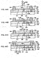
- the liquid discharge head 22 has a nozzle line 28 comprising a plurality of nozzles 27 , as shown, for example, in FIG. 10.
- the number of nozzles 27 is, for example, 180, and the diameter of the nozzles 27 is, for example, 28 ⁇ m.
- the pitch t between the nozzles 27 is, for example, 141 ⁇ m.
- the width direction M shown in FIG. 10 designates a standard direction in which the liquid discharge head sweeps, and the aligning direction T designates a direction in which the nozzles 27 in the nozzle line 28 align.
- the liquid discharge head 22 has a nozzle plate 29 formed of stainless steel or the like, a diaphragm 31 opposing the nozzle plate 29 , and a plurality of partition members 32 joining the nozzle plate 29 to the diaphragm 31 , for example, as shown in FIG. 12( a ) and FIG. 12( b ).
- the partition members 32 define a plurality of ink chambers 33 and a liquid pool 34 between the nozzle plate 29 and the diaphragm 31 .
- the ink chambers 33 communicate with the liquid pool 34 through passages 38 .
- the diaphragm 31 is provided with an ink supply port 36 in a proper position thereof.
- the ink supply port 36 is connected to an ink supply device 37 .
- the ink supply device 37 supplies a filter element material M for one of R, G, and B colors, which may be an R-color filter element material, to the ink supply port 36 .
- the supplied filter element material M fills the liquid pool 34 and then flows through the passages 38 to fill the ink chambers 33 .
- the nozzle plate 29 has nozzles 27 for jetting the filter element material M from the ink chambers 33 .
- Ink pressurizers 39 are disposed, corresponding to the ink chambers 33 , on the back surface of the diaphragm 31 opposite the surface opposing the ink chambers 33 .
- the ink pressurizers 39 each have a piezoelectric element 41 and a pair of electrodes 42 a and 42 b separated by the piezoelectric element 41 , as shown in FIG. 12( b ).
- the piezoelectric element 41 is bent in the external direction designated by the arrow C by energization so that the volume of the corresponding ink chamber 33 increases. Accordingly, the filter element material M flows in an amount equivalent to the increased volume from the liquid pool 34 into the ink chamber 33 through the passage 38 .
- ink-repellent films 43 formed of, for example, Ni-tetrafluoroethylene eutectoid by plating are provided in the regions surrounding the nozzles 27 for preventing droplets 8 from being discharged in a wrong direction and from clogging the nozzles 27 .
- the head position controller 17 includes an ⁇ motor 44 for horizontally rotating the liquid discharge head 22 incorporated in the head unit 26 , a ⁇ motor 46 for rotating the liquid discharge head 22 with reciprocation on an axis parallel to the shifting direction Y, a ⁇ motor 47 for rotating the liquid discharge head 22 with reciprocation on an axis parallel to the sweeping direction X, and a z motor 48 for moving the liquid discharge head 22 in the vertical direction.
- the substrate position controller 18 includes a table 49 on which the mother substrate 12 is placed and a ⁇ motor 51 for horizontally rotating the table 49 .
- the sweeping driver 19 has an X guide rail 52 extending in the sweeping direction X and an X slider 53 containing, for example, a pulse-driven linear motor.
- the X slider 53 moves in the sweeping direction X along the X guide rail 52 by, for example, activating the linear motor contained therein.
- the shifting driver 19 has a Y guide rail 54 extending in the shifting direction Y and a Y slider 56 containing, for example, a pulse-driven linear motor.
- the Y slider 56 moves in the shifting direction Y along the Y guide rail 54 by, for example, activating the linear motor contained therein.
- the linear motors contained in the X and Y sliders 53 and 56 can precisely control rotation angles of the output shafts by pulse signals applied thereto. Consequently, the position of the liquid discharge head 22 , which is supported by the X slider 53 , in the sweeping direction X and the position of the table 49 in the shifting direction Y can be controlled with high accuracy.
- the positions of the liquid discharge head 22 and the table 49 may be controlled by feedback with a servomotor or other desired methods, and the control of the positions is not limited to that by the pulse motor.
- the table 49 is provided with positioning pins 50 a and 50 b thereon for controlling the horizontal position of the mother substrate 12 .
- the mother substrate 12 is positioned by the substrate feeding device 23 , which will be described later, such that end faces thereof in the sweeping direction X and the shifting direction Y are pressed to the positioning pins 50 a and 50 b .
- the table 49 has known fixing means for fixing the positioned mother substrate 12 by, for example, air aspiration (vacuum drawing).
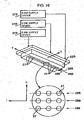
- the liquid discharge device 16 of the present embodiment is provided with a plurality of pairs (two pairs in the drawing) of imaging devices 91 R and 91 L and 92 R and 92 L above the table 49 , as shown in FIG. 9.
- the drawing illustrates only the barrels of the imaging devices 91 R and 91 L and 92 R and 92 L, and the other parts and the structure of supporting the imaging devices are omitted.
- the imaging devices used for observation may be CCD cameras.
- FIG. 8 does not show the imaging devices.
- FIGS. 22 ( a ) and 22 ( b ) are plan views of the mother substrate 12 positioned on and supported by the table 49 .
- the mother substrate 12 may be supported on the table 49 such that the longitudinal direction L thereof is parallel to the sweeping direction X when viewed from above, as shown in FIG. 22( a ), or such that the longitudinal direction L is parallel to the shifting direction Y, as shown in FIG. 22( b ).
- the positioning pins 50 a here in the drawing, can move in the horizontal direction of the drawing according to the horizontal position of the mother substrate 12 and the positioning pins 50 b are fixed on the table 49 .
- both the positioning pins 50 a and 50 b may be fixed on the table 49 , as in the positioning pins 50 b , or movable, as in the positioning pins 50 a.
- the mother substrate 12 is previously provided with two pairs, and a total of four, of alignment marks 12 ar and 12 al and 12 br and 12 bl in the outer region thereof.
- the alignment marks 12 ar and 12 al are provided at both sides of the mother substrate 12 in the longitudinal direction L, respectively.
- the alignment marks 12 br and 12 bl are provided at both sides of the mother substrate 12 in the width-extending direction, that is, in the width direction M, respectively.
- the imaging devices 91 R and 91 L and 92 R and 92 L are each directly or indirectly fixed to a fixing portion (for example, the base 9 ) of the liquid discharge device 16 .
- a fixing portion for example, the base 9
- the position of the mother substrate 12 on the table 49 are accurately detected by observing the mother substrate 12 with the fixed imaging devices.
- the mother substrate feeding device 23 shown in FIG. 8 includes a mother substrate holder 57 for accommodating mother substrates 12 and a mother substrate carrier 58 for carrying the mother substrates 12 , such as a robot.
- the mother substrate carrier 58 includes a base 59 , an up-and-down shaft 61 rising and lowering with respect to the base 59 , a first arm 62 rotating on the up-and-down shaft 61 , a second arm 63 rotating on the basis of the movement of the first arm 62 , and a sucking pad 64 provided on the undersurface of the end of the second arm 63 .
- the sucking pad 64 is intended to hold the mother substrate 12 by air aspiration (vacuum drawing) or the like.
- a capping device 76 and a cleaning device 77 are disposed at one side of the shifting driver 21 and under the sweeping locus of the liquid discharge head 22 , as shown in FIG. 8. Furthermore, an electronic balance 78 is disposed at the other side of the shifting driver 21 .
- the capping device 76 is intended to prevent the nozzles 27 (see FIG. 10) from drying while the liquid discharge head 22 is in standby.
- the cleaning device 77 is intended to clean the liquid discharge head 22 .
- the electronic balance 78 is intended to weigh the ink droplet 8 discharged from each nozzle 27 .
- a head camera 81 shifting together with the liquid discharge head 22 is attached in the vicinity of the liquid discharge head 22 .
- the control apparatus 24 shown in FIG. 8 includes a computer main body 66 containing a processor, an input device 67 , such as a keyboard, and a display device 68 , such as a CRT.
- the computer main body 66 includes a CPU (central processing unit) 69 shown in FIG. 14 and an information-recording medium 71 serving as a memory for storing various types of information.
- the head position controller 17 , the substrate position controller 18 , the sweeping driver 19 , the shifting driver 21 , and a head driving circuit 72 for driving the piezoelectric elements 41 (see FIG. 12( b )) in the liquid discharge head 22 are connected to the CPU 69 through an input-output interface 73 and a bus 74 , as shown in FIG. 14.
- the substrate feeding device 23 , the input device 67 , the display device 68 , the capping device 76 , the cleaning device 77 , and the electronic balance 78 are also connected to the CPU 69 through the input-output interface 73 and the bus 74 , as in above.
- Memories such as the information-recording medium 71 , generally include semiconductor memories, such as a RAM (random access memory) and a ROM (read only memory), and external storages, such as a hard disk, a CD-ROM reading device, and a disk-shaped recording medium.
- the information-recording medium 71 has: memory areas for storing software in which procedures for controlling the liquid discharge device 16 are programmed, coordinate data defining positions in the mother substrate 12 to which the liquid discharge head 22 discharges ink, and the distance at which the mother substrate 12 is shifted in the shifting direction Y in FIG. 9; areas for functioning as a working area of the CPU 69 , temporary files, and the like; and other various memory areas.
- the CPU 69 functions as a control to discharge ink in predetermined positions on the surface of the mother substrate 12 , according to the software stored in the memory, or the information recording medium 71 .
- the CPU 69 has a cleaning operation part for performing arithmetic computation for cleaning, a capping operation part for performing capping operation, a weighing operation part for performing arithmetic computation for measuring weight with the electronic balance 78 , and a drawing operation part for drawing a predetermined pattern by discharging ink droplets onto the surface of the mother substrate 12 , as shown in FIG. 14.
- the drawing operation part has various controlling operation parts for performing arithmetic computations such as a drawing initial position operating part for locating the liquid discharge head 22 at an initial position, a sweeping control operation part for sweeping the liquid discharge head 22 in the sweeping direction X at a predetermined speed, a shifting operation part for shifting the mother substrate 12 a predetermined distance in the shifting direction Y, and a nozzle discharge control operation part for determining which of the plurality of nozzles 27 of the liquid discharge head 22 discharges ink.
- various controlling operation parts for performing arithmetic computations such as a drawing initial position operating part for locating the liquid discharge head 22 at an initial position, a sweeping control operation part for sweeping the liquid discharge head 22 in the sweeping direction X at a predetermined speed, a shifting operation part for shifting the mother substrate 12 a predetermined distance in the shifting direction Y, and a nozzle discharge control operation part for determining which of the plurality of nozzles 27 of the liquid discharge head 22 discharges ink.
- control functions are embodied by software used with the CPU 69 , in the embodiment. However, these functions may be embodied by an electronic circuit, but not CPUs, if such an electronic circuit is applicable.
- step S 1 initialization is performed in step S 1 . Specifically, the head unit 26 , the substrate feeding device 23 , control apparatus 24 , and other devices are restored to the initial settings.
- step S 2 When weighing timing comes (step S 2 ), the sweeping driver 19 moves the head unit 26 shown in FIG. 9 to the position of the electronic balance 78 shown in FIG. 8 (step S 3 ).
- the electronic balance 78 weighs the ink droplet discharged from the nozzles 27 (step S 4 ). Voltage applied to the piezoelectric elements 41 of the nozzles 27 is adjusted according to the ink-discharge performance of the nozzles 27 evaluated by the weigh (step S 5 ).
- step S 6 When cleaning timing comes (step S 6 ), the sweeping driver 19 moves the head unit 26 to the cleaning device 77 (step S 7 ). The cleaning device 77 cleans the liquid discharge head 22 (step S 8 ).
- the substrate feeding device 23 shown in FIG. 8 is activated to feed the mother substrate 12 to the table 49 in step S 9 .
- the sucking pad 64 draws one of the mother substrates 12 in the mother substrate holder 57 to hold it up.
- the up-and-down shaft 61 , the first arm 62 , and the second arm 63 are moved to carry the mother substrate 12 to the table 49 and, then, press the mother substrate 12 to the pins 50 a and 50 b (see FIG. 9) previously provided in proper places on the table 49 .
- the table 49 is horizontally rotated to position the mother substrate 12 by rotating the output shaft of the ⁇ motor 51 in small angles (step S 10 ). More specifically, the pairs of imaging devices 91 R and 91 L and 92 R and 92 L shoot the alignment marks 12 ar and 12 al and 12 br and 12 bl provided at the sides of the mother substrate 12 .
- the horizontal posture of the mother substrate 12 is calculated from the positions where the alignment marks are shot.
- the rotation angle ⁇ is adjusted by rotating the table 49 according to the horizontal posture of the mother substrate 12 .
- step S 11 the position where the liquid discharge head 22 starts drawing is determined by calculation.
- step S 12 the shifting driver 21 .
- the standard direction S shown in FIG. 10 of the liquid discharge head 22 is not necessarily parallel to the sweeping direction X, and it may form an angle ⁇ 1 or ⁇ 2 with respect to the sweeping direction X, as shown in FIGS. 1 and 2.
- These angles ⁇ 1 and ⁇ 2 are intended to geometrically equalize the pitch of the nozzles 27 arranged in the T direction to the pitch of droplets landing on the mother substrate 12 in the shifting direction Y because the pitch of the ink droplets to be discharged onto the surface of the mother substrate 12 is often different from the pitch of the nozzles 27 .
- step S 12 When the liquid discharge head 22 is placed in the starting position of drawing in step S 12 shown in FIG. 15, the liquid discharge head 22 is linearly moved to sweep in the sweeping direction X at a constant speed in step S 13 .
- the liquid discharge head 22 continuously discharges ink droplets from the nozzles 27 thereof onto the surface of the mother substrate 12 during sweeping.
- the amount of an ink droplet may be set such that the entire amount of ink is discharged to an area covered by a series of sweeping operation of the liquid discharge head 22 .
- the amount of the ink droplet may be set such that a fraction (for example, one fourth) of the entire amount of ink required in one series of sweeping operation is discharged.
- the sweeping operation is repeated several times (for example, four times) so as to overlap parts of sweeping areas in the shifting direction Y and to cover the entire area where the ink should be discharged.
- step S 14 After the completion of a series of sweeping on the mother substrate 12 (step S 14 ), the liquid discharge head 22 reverses the shifting direction to return to the initial position (step S 15 ), and shifts a predetermined distance (by a shifting distance set in advance) in the shifting direction Y (step S 16 ). The ink is then swept again and discharged in step S 13 , and the above-described procedure is repeated to sweep over a plurality of lines.
- the liquid discharge head 22 may be driven so as to shift a predetermined distance in the shifting direction Y and, then, turn to sweep in the opposite direction, as described later with reference to FIG. 2.
- the liquid discharge head 22 shifts a predetermined distance in the shifting direction Y after the completion of ink discharge to the entirety of a line over the color filter regions on the mother substrate 12 (step S 17 ), and repeats steps S 13 to S 16 .
- the substrate feeding device 23 or another transport means carries the treated mother substrate 12 to the outside in step S 20 . Then, the feed of the mother substrate 12 and the discharge of ink are repeated as in above until an operator give a direction to terminate the procedure.
- step S 21 When the operator directs the CPU 69 to terminate the procedure (step S 21 ), the liquid discharge head 22 is carried to the capping device 76 .
- the capping device 76 caps the liquid discharge head 22 (step S 22 ).
- ink can land on the entire surface of the mother substrate 12 by continuously discharging ink droplets while the liquid discharge head 22 sweeps in the sweeping direction X and by shifting the sweeping operation in the shifting direction Y and then repeating the sweeping operation.
- the mother substrate 12 on the table 49 can be positioned using the imaging devices 91 R and 91 L which shoot the alignment marks 12 ar and 12 al , as shown in FIG. 22( a ).
- the mother substrate 12 put on the table 49 in a different horizontal posture (the posture in which the mother substrate 12 is rotated 90° on the normal thereof) can be positioned using the imaging devices 92 R and 92 L which shoot the alignment marks 12 br and 12 bl , as shown in FIG. 22( b ). Therefore, two different sweeping directions X (perpendicular to each other) can be set with respect to the mother substrate 12 .
- mother substrates 12 having various ink-landing-position arrangements are fed to the liquid discharge device 16 .
- the size of the unit regions 11 or the dot array pattern may be varied between product models, or the arrangement manner of the unit regions 11 may be varied in order to increase productivity by increasing the number of unit regions 11 as many as possible.
- the liquid discharge device 16 can treat the mother substrate 12 regardless of the horizontal posture in which the mother substrate 12 is placed in either of the two different directions as shown in FIGS. 22 and 23 (perpendicular to each other in the drawings), the mother substrate 12 can be placed on the table 49 in a horizontal posture according to the ink-landing-position arrangement. As a result, the liquid discharge device 16 can efficiently treat a discharge object, or the mother substrate 12 , according to the posture of the object.
- the substrate feeding device 23 is used for placing the mother substrate 12 on the table 49 .
- the feeding posture of the substrate feeding device 23 may be changed.
- a mechanism for rotating the table 49 may be used to rotate it, for example, 90°, and whether the horizontal orientation of the mother substrate 12 is changed is selected after the mother substrate 12 is placed on the table 49 .
- the amount of ink droplets discharged from the nozzles 27 constituting the nozzle line 28 of the liquid discharge head 22 is liable to vary, and, for example, that some nozzles 27 at both ends of the nozzle line 28 (for example, 10 nozzles at each end) particularly discharge a large amount of ink. It is not preferable to use the nozzles 27 discharging ink in an amount larger than that of the other nozzles 27 because it results in films having nonuniform thicknesses.
- nozzles 27 constituting the nozzle line 28 , at both ends E of the nozzle line 28 so as not to discharge ink and to use the other nozzles in the other region F, as shown in FIG. 13.
- each film is formed of a plurality of droplets from the liquid discharge head 22 , but not only one droplet, in a predetermined region. Specifically, in the case of depositing films in a plurality of regions, even if with a certain variety in the amount of each of droplets by forming the films of a plurality of droplets, the nonuniformity of the film thickness in each region can be reduced.
- the structure of the liquid discharge head 22 is not limited to the one described above, but various structures may be applied.
- a liquid discharge head 22 A shown in FIG. 11 has two nozzle lines 28 disposed in the standard direction S. Each of these nozzle lines 28 includes a plurality of nozzles 27 , as in above.
- Another liquid discharge head 22 B shown in FIG. 16 has three nozzle lines 28 R, 28 G, and 28 B disposed in the standard direction S.
- the liquid material discharged from the nozzles 27 in the nozzle lines 28 may be the same or different between the lines.
- the nozzles 27 in both nozzle lines 28 discharge the same ink.
- the material of ink discharged from the nozzles 27 is different between the nozzle lines 28 R, 28 G, and 28 B such that, for example, filter element materials 13 R, 13 G, and 13 B are discharged, as described later.
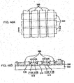
- FIG. 5( a ) schematically shows the plan structure of an exemplary color filter.
- FIG. 6( d ) shows the structure in a sectional view taken along line VI-VI of FIG. 5( a ).
- the color filter 1 of the present embodiment includes a substrate (base material) 2 formed of glass, resin, or the like and a plurality of filter elements 3 deposited on the surface of the substrate 2 , in a dot pattern, which may be a dot matrix as shown in the drawing.
- the color filter 1 also includes a protective layer 4 deposited on the filter elements 3 , as shown in FIG. 6( d ).
- FIG. 5( a ) shows the color filter 1 without the protective layer 4 in plan view.
- Barrier walls 6 are formed of a light-shielding resin in a grid pattern on the substrate 2 .
- the regions partitioned by the barrier walls 6 are filled with a color material to form filter elements 3 .
- the filter elements 3 are each formed of one of the color materials of R (red), G (green), and B (blue), and the resulting filter elements 3 each having one of the colors are arrayed in a predetermined arrangement. Exemplary arrangements include striped arrangement (in which all the filter elements in a column in the matrix have the same color) shown in FIG. 7( a ), mosaic arrangement (in which any series of three filter elements 3 aligned in a column or a row includes R, G, and B colors) shown in FIG.
- the “barrier walls” in the present invention include “banks”, referring to protrusions from the substrate, and the side faces thereof may be substantially perpendicular to the substrate or sloped.
- the color filter 1 has a size of, for example, about 4.57 cm (1.8 inches).
- the filter elements 3 each have dimensions of 30 ⁇ m ⁇ 100 ⁇ m.
- the interval between adjacent filter elements 3 that is, the filter element pitch, is, for example, 75 ⁇ m.
- the color filter 1 of the present invention When the color filter 1 of the present invention is used as an optical element for displaying color images (full color images), three filter elements of R, G, and B colors constitute a unit acting as a pixel. Color images are displayed by selectively passing light through one of the R, G, and B filter elements in a pixel or a combination of the filter elements.
- the barrier walls 6 formed of a light-shielding resin serve as a black matrix.
- the color filter 1 is cut off from the substrate, that is, the mother substrate 12 having a large area as shown in FIG. 5( b ). Specifically, a color filter pattern is formed in each of a plurality of color-filter-forming regions (unit regions) 11 defined in the mother substrate 12 . Grooves for cutting into pieces are formed in the surroundings of the color-filter-forming regions 11 .
- the mother substrate 12 is divided (cut) into pieces to form the color filters 1 , one of which is shown in FIG. 5( a ), by applying a stress to the grooves or other methods.
- FIG. 6 schematically shows a procedure of manufacturing the color filter 1 step by step.
- the barrier walls 6 are formed of a light-shielding resin in a grid pattern viewed in the direction of arrow B, on the mother substrate 12 .
- the hollows 7 of the grid pattern define regions where the filter elements 3 are formed, that is, filter-element-forming regions.
- the plan dimension of each filter-element-region 7 separated by the barrier walls 6 is, for example, 30 ⁇ m ⁇ 100 ⁇ m, when viewed in the direction of arrow B.
- the barrier walls 6 serve to stop the flow of a liquid filter element material 13 and as a black matrix. Also, the barrier walls 6 are formed by an arbitrary patterning technique, such as photolithography, and may further be heated with a heater if necessary.
- the droplets 8 of the filter element material 13 are supplied to the filter-element-forming regions 7 as shown in FIG. 6( b ).
- the filter-element-regions 7 are filled with the filter element material 13 .
- This process is performed by, for example, discharging the droplets 8 of the ink (filter element material 13 ) from the liquid discharge head 22 of the above-described liquid discharge device 16 to deposit the droplets 8 in the filter-element-forming regions 7 .
- Reference numerals 13 R, 13 G, and 13 B in FIG. 6( b ) represent filter element materials having R (red), G (green), and B (blue) colors, respectively.
- the mother substrate 12 is heated to, for example, about 70° C. by a heater to vaporize the solvent of the filter element material 13 .
- This vaporization reduces the volume of the filter element material 13 and, thus, the filter element material 13 become flattened, as shown in FIG. 6( c ). If the volume is excessively reduced, the supply of the droplets 8 of the color filter material 13 and the heating of the droplets 8 are repeated until the thickness of filter element material reaches a level satisfactory for the resulting color filter 1 . Only the remaining solid constituents of the color filter material 13 result in a film, thus forming the color filter elements 3 , each having a desired color.
- the color filter elements 3 are subjected to heat treatment at a predetermined temperature for a predetermined time to be completely dried.
- the protective layer 4 is deposited by a proper method, such as spin coating, roll coating, dipping, or ink jetting.
- the protective layer 4 is intended to protect the filter elements 3 and flatten the surface of the color filter 1 .
- the barrier walls 6 are formed of a light-shielding resin to serve to block light (as a black matrix).
- barrier walls 6 may be covered with a light-shielding layer formed of a metal, such as Cr, having a size larger than that of the barrier walls thereunder.
- the filter element material 13 is used as ink discharged from the above-described liquid discharge device 16 , and the droplets 8 of the ink are deposited in the filter-element-forming regions 7 to from the filter element 3 .
- the three types of filter element material 13 R, 13 G, and 13 b are discharged together while the liquid discharge head 22 is swept in an identical sweeping direction X with respect to the mother substrate 12 , unevenness occurs in a striped manner in the sweeping direction X due to the variation of the discharge rate between the nozzles 27 of the liquid discharge head 22 , as described above, and changes of the discharge rate of the nozzles 27 with time.
- any one of the three types of filter element material 13 R, 13 G, and 13 B is discharged while the liquid discharge head 22 is swept in a different direction from that for the other types of filter element materials.
- two of the above-described three color materials are discharged while the liquid discharge head 22 is swept in a sweeping direction X parallel to the longitudinal direction L of the mother substrate 12 , as shown in FIG.
- the sweeping direction for discharge of one of the three types of filter element material 13 R, 13 G, and 13 B differs from (and becomes perpendicular to) the sweeping direction for the others, with respect to the mother substrate 12 .
- the striped color shading of one color material occurs in a direction different from that of the other color materials and, thus, the color shading of the color filter 1 becomes inconspicuous on the whole, effectively decreasing.
- FIGS. 1 to 4 are schematic illustrations showing procedures for discharging the above-described filter element materials 13 R, 13 G, and 13 B onto the mother substrate 12 from the nozzles 27 of the liquid discharge head 22 .
- FIG. 24 is a schematic illustration of the structure of a manufacturing apparatus for performing the procedures.
- the apparatus for manufacturing color filters shown in FIG. 24 includes first, second, and third sections 16 R, 16 G, and 16 B, each including substantially the same liquid discharge device 16 . Only the first section 16 R includes a substrate holder 57 but the second and third sections 16 G and 16 B do not. Preliminary dryers 96 each having a hot plate are disposed for preliminarily drying inks (filter element materials) discharged and deposited on the mother substrate 12 , between the first and second sections 16 R and 16 G, between the second and third sections 16 G and 16 B, and downstream of the third section 16 B.
- a substrate carrier 58 for carrying the mother substrate 12 to the corresponding section and another substrate carrier 95 for carrying the mother substrate from the upstream liquid discharge device to the following preliminary dryer 96 are disposed corresponding to each of the sections. Furthermore, a substrate exporter 97 is disposed for carrying the mother substrate 12 from the preliminary dryer 96 located downstream of the third section 16 B to another substrate holder 98 .
- the first section 16 R discharges the R (red) filter element material 13 R onto the mother substrate 12 , and subsequently the corresponding preliminary dryer 96 dries the filter element material 13 R. Then, the second section 16 G discharges the G (green) filter element material 13 G onto the mother substrate 12 , and the corresponding preliminary dryer 96 dries the filter element material 13 G. Furthermore, the third section 16 B discharges the B (blue) filter element material 13 B onto the mother substrate 12 , and the corresponding preliminary dryer 96 dries the filter element material 13 B. The resulting filter elements 3 R, 3 G, and 3 B are finally stored in the substrate holder 98 .
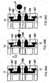
- FIG. 1 shows a concrete example of the manufacturing process performed to the mother substrate 12 by the above-described sections 16 R, 16 G, and 16 B of the manufacturing apparatus.
- the position of the liquid discharge head 22 is illustrated as if displaced in the sweeping direction when the liquid discharge head 22 is shifted in the shifting direction, for the sake of illustration convenience. However, this does not necessarily mean that the starting point of sweeping is changed from one series of sweeping to another.
- the filter-element-forming regions 7 are arranged in a dot matrix manner in each color-filter-forming region (unit region) 11 of the mother substrate 12 .
- the longitudinal direction L and width direction M of the mother substrate are set as shown in FIG. 12.
- One or two color materials (for example, 13 R or 13 R and 13 G) of the filter element materials 13 R, 13 G, and 13 B are continuously discharged to serve as ink from the liquid discharge head 22 which is simultaneously swept in the longitudinal direction L from the external position (initial position) of one end of the mother substrate 12 in the longitudinal direction L (the left end in the drawing), so that the droplets of the ink land in the filter-element-forming regions aligning in the longitudinal direction L.
- the liquid discharge head 22 When the liquid discharge head 22 reaches the other end (the right end, but not shown, in the drawing) of the mother substrate 12 , it is shifted a predetermined distance in the width direction M, and subsequently returns to the external position of the former end. The liquid discharge head 22 again discharges droplets while being swept in the longitudinal direction L.
- the other two or one color material (for example, 13 G and 13 B or 13 B) of the filter element materials 13 R, 13 G, and 13 B is discharged onto the mother substrate 12 while the liquid discharge head 22 is swept in the width direction M from the external position of at one end of the mother substrate 12 as the initial position of the liquid discharge head 22 in the width direction M.
- the liquid discharge head 22 is shifted a predetermined distance in the longitudinal direction L, and is subsequently moved in the opposite direction to return to the external position at the end in the width direction M of the mother substrate 12 . This operation is repeated.
- at least one color material of the three filter element materials 13 R, 13 G, and 13 B is discharged in a sweeping direction different from (perpendicular to) the sweeping direction for the other color materials.
- FIG. 2 shows another manufacturing process performed by the sections 16 R, 16 G, and 16 B of the manufacturing apparatus, according to a modification of Variation 1.
- one or two color materials of the filter element materials 13 R, 13 G, and 13 B are discharged in a scanning direction of the liquid discharge head 22 parallel to the above-described longitudinal direction L, and the other color material(s) is discharged in a different sweeping direction of the liquid discharge head 22 parallel to the above-described width direction M.
- This example is, however, different from the method shown in FIG. 1 in that after one series of the sweeping in which the liquid discharge head 22 sweeps in the longitudinal direction L or the width direction M from the external position at one end of the mother substrate 12 to the other end is completed, and the shifting operation is made at the external position of the other end of the mother substrate 12 , the liquid discharge head 22 reverses the sweeping direction (the longitudinal direction L or width direction M) at the external position of the other end of the mother substrate 12 , thus discharging droplets. By repeating this operation, the liquid discharge head 22 can sweep on the mother substrate 12 in two directions opposite to each other, consequently not needing returning operation. Thus, more efficient manufacturing can be performed.
- the pitches of the filter-element-forming regions (unit regions) 11 of the mother substrate 12 in the longitudinal direction L and the width direction L may be different from each other, in the embodiment shown FIGS. 1 and 2.
- the angles ⁇ 1 and ⁇ 2 between the standard direction S and scanning direction X (parallel to the longitudinal direction L or width direction M in the drawings) of the liquid discharge head 22 may be changed between the sweeping operation with the same liquid discharge head 22 in the longitudinal direction L and the width direction M, as shown in FIGS. 1 and 2.
- FIG. 3 is a schematic illustration showing a sweeping manner of the liquid discharge head 22 different from that described above.
- the position of the liquid discharge head 22 is illustrated as if displaced in the sweeping direction when the liquid discharge head 22 is shifted in the shifting direction, for the sake of illustration convenience. However, this does not necessarily mean that the starting point of sweeping is changed from one series of sweeping to another.
- the liquid discharge head 22 discharges droplets 8 of ink (filter element material) such that N droplets 8 (4 drops in the drawing) land in each filter-element-forming region 7 to form the corresponding filter element 3 .
- the amount of a droplet 8 discharged from the liquid discharge head 22 and the volume of the filter elements 3 are set in advance.
- the amount of the filter element material discharged in each filter-element-forming region 7 is 1/N (1/4 in the drawing) of the entirety of a desired quantity during a series of sweeping.
- the droplet 8 is discharged N times (4 times in the drawing) in the filter-element-forming region 7 and, thus, the entire quantity of the filter element material fills the filter-element-forming region 7 .
- the liquid discharge head 22 may be swept over the mother substrate 12 to discharge droplets 8 in both directions even in a reciprocating manner as in the case shown in FIG. 2.
- the plurality of liquid discharge heads 16 R, 16 G, and 16 B are used for the plurality of filter element materials 13 R, 13 G, and 13 B, respectively, and the sweeping direction of at least one liquid discharge head (ink jet head) 22 is set different from that of the other heads by changing the posture of the mother substrate 12 fed.
- the method of the present invention is not limited to the method above, but a plurality of filter element materials may be discharged one by one from only one liquid discharge device. Specifically, the relative orientation between the mother substrate 12 and the sweeping direction of the liquid discharge head 22 is changed in one liquid discharge device, during the discharging process.
- the sweeping direction of the liquid discharge head may be changed during the discharging process to change the relative orientation.
- the liquid discharge head (ink jet head) 22 can sweep not only the sweeping direction X shown in FIG. 9 but also in the shifting direction Y
- the horizontal orientation of the mother substrate 12 may be changed during the discharging process to change the relative orientation. Both techniques may be applied in the present invention, and the latter will now be illustrated in detail with reference to FIG. 25.
- FIG. 25 shows a state in which the mother substrate 12 is placed on the table 49 of the liquid discharge device 16 shown in FIGS. 8 and 9.
- the orientations of the mother substrate 12 in which the longitudinal direction L of the mother substrate 12 is parallel to the sweeping direction X (shown in (a) and (b) of FIG. 25) and in which the width direction M of the mother substrate 12 is parallel to the sweeping direction X (shown in (c) of FIG. 25) are switched by rotating the table 49 .
- the sweeping direction X of the liquid discharge head 22 is relatively rotated 90° with respect to the mother substrate 12 .
- the substrate feeding device 23 shown in FIG. 8 feeds the mother substrate 12 onto the table 49 , first.
- the mother substrate 12 is placed on the table 49 such that the longitudinal direction L of the mother substrate 12 becomes parallel to the sweeping direction X of the liquid discharge head 22 , as shown in FIG. 25( a ).
- the liquid discharge head 22 discharges the filter element material 13 R from the nozzles 27 thereof.
- the liquid discharge head 22 discharges another filter element material 13 G in the same posture, in the same manner as above, as shown in FIG. 25( b ).
- the sweeping operation and the shifting operation as in above, all the necessary filter-element-forming regions 7 are filled with the filter element material 13 G to form the filter elements 3 G.
- the table 49 is rotated 90°, as shown in FIG. 25( c ).
- the mother substrate 12 on the table 49 is held in a horizontal orientation in which the width direction M thereof is parallel to the sweeping direction X of the liquid discharge head 22 .
- the liquid discharge head 22 discharges the other filter element material 13 B as in above.
- liquid discharge head 22 B can discharge the filter element materials 13 R, 13 G, and 13 B supplied from three ink supply devices 37 R, 37 G, and 37 B respectively, from the nozzles 27 of the three respective nozzle lines 28 R, 28 G, and 28 B.
- the single liquid discharge head 22 B can, therefore, perform the above-described three steps.
- a plurality of droplets are discharged in each filter-element-forming region 7 .
- some of the plurality of droplets for one filter-element-forming region 7 may be discharged in a sweeping direction, with respect to the mother substrate 12 , different from the sweeping direction for the other droplets.
- the variation of the quantity of ink filling each filter-element-forming region 7 resulting from discharging a plurality of ink droplets can be reduced.
- color shading resulting from the sweeping direction can be reduced.
- FIG. 26 shows an exemplary process of discharging a plurality of droplets of an identical type of filter element material in each filter-element-forming region 7 , as in above. For example, some (two drops in the drawing) of N droplets 8 (4 drops in the drawing) which should be discharged in the filter-element-forming region 7 are discharged while the ink jet head is sweeping over the mother substrate 12 in a horizontal posture in which the longitudinal direction L thereof is parallel to the sweeping direction X, as shown in FIG. 26( a ).
- the other droplets 8 are discharged while the ink jet head is sweeping over the mother substrate 12 in another horizontal posture in which the width direction M thereof is parallel to the sweeping direction X, as shown in FIG. 26( b )
- FIG. 4 A concrete example of Variation 3 will now be illustrated with reference to FIG. 4.
- the position of the liquid discharge head 22 is illustrated as if displaced in the sweeping direction when the liquid discharge head 22 is shifted in the shifting direction, for the sake of illustration convenience. However, this does not necessarily mean that the starting point of sweeping is changed from one series of sweeping to another.
- the sweeping direction of the liquid discharge head is preferably set in a direction different from (perpendicular to) the sweeping direction when the other, R (red) and G (green), filter elements 3 R and 3 G are formed.
- the Variations described above are not limited to the manufacturing of a color filter, but they may be applied to the manufacturing of an EL device. In addition, they may be applied to various methods for film deposition and structures of a film forming devoice.
- the liquid discharge head 22 is repeatedly swept while being shifted in distances equivalent to the discharge width of the liquid discharge head 22 .
- the error variance method may be employed in which the liquid discharge head 22 is repeatedly swept while being shifted in distances smaller than the above-described discharge width, in order to reduce the unevenness of film deposition resulting from the variation of the discharge quantity between the plurality of nozzles of the liquid discharge head 22 .
- the unevenness of film deposition can further be reduced.
- FIG. 17 shows a method for manufacturing a liquid crystal device according to an embodiment of a method for manufacturing a display device (electro-optic device) of the present invention.
- FIG. 18 shows a liquid crystal device, by way of example of a display device (electro-optic device) manufactured by the method.
- FIG. 19 is a cross sectional view of the liquid crystal device taken along line IX-IX in FIG. 18.
- the liquid crystal device here is a simple matrix-type transflective liquid crystal device displaying full color images.
- the liquid crystal device 101 has a liquid crystal panel 102 containing liquid crystal driving ICs 103 a and 103 b formed in a semiconductor chip and an FPC (flexible printing circuit) 104 connected to the liquid crystal panel 102 .
- the liquid crystal device 101 also has an illumination device 106 , acting as a backlight, at the rear surface side of the liquid crystal panel 102 .
- the liquid crystal panel 102 includes a first substrate 107 a and a second substrate 107 b bonded to each other with a sealant 108 .
- the sealant 108 is formed by, for example, screen-printing an epoxy resin in a loop (circular manner) on the inner surface of the first substrate 107 a or the second substrate 107 b .
- the sealant 108 contains spherical or cylindrical conductors 109 formed of a conductive material and dispersed therein, as shown in FIG. 19.
- the first substrate 107 a has a transparent plate-like base 111 a formed of glass, resin, or the like, as shown in FIG. 19.
- the base 111 a is provided with a reflecting layer 112 on the inner surface (upper surface in FIG. 19) thereof.
- An insulating layer 113 is deposited on the reflecting layer 112 , and first electrodes 114 a are formed on the insulating layer 113 in a striped manner (see FIG. 18) when viewed in the direction indicated by arrow D.
- an alignment layer 116 a overlies the electrodes.
- a polarizer 117 a is provided on the outer surface (lower surface in FIG. 19) of the base 111 a by adhesion.
- the distances between the first electrodes 114 a shown in FIG. 18 are illustrated considerably larger than the actual distances, for the sake of ease of understanding the arrangement. Hence, the number of the first electrodes 114 a overlying the base 111 is, in practice, larger than the number of the first electrodes 114 a shown in the drawing.
- the second substrate 107 b has a transparent plate-like substrate 111 b formed of glass, resin, or the like, as shown in FIG. 19.
- a color filter 118 is disposed on the inner surface (lower surface in FIG. 19) of the base 111 b , and second electrodes 114 are formed on the color filter 118 in a striped manner (see FIG. 18) in a direction perpendicular to the first electrodes 114 a .
- an alignment layer 116 B overlies the electrodes.
- a polarizer 117 b is provided on the outer surface (upper surface in FIG. 19) of the base 111 b by adhesion.
- a so-called cell gap which is the space enclosed with the first substrate 107 a , the second substrate 107 b , and the sealant 108 , is filled with a liquid crystal L, such as STN (super twisted nematic) liquid crystal.
- a liquid crystal L such as STN (super twisted nematic) liquid crystal.
- the first electrodes 114 a and the second electrodes 114 b extend so as to intersect each other. Their intersections in plan view are arrayed in a dot matrix when viewed in the direction indicated by arrow D in FIG. 19. The intersections each form a display dot.
- the color filter 118 has R (red), G (green), and B (blue) elements (filter elements) arranged in a predetermined pattern, such as a striped arrangement, a delta arrangement, or a mosaic arrangement. Each display dot corresponds to one element of R, G, and B filter elements. Three display dots of R, G, and B define a pixel.
- Images are displayed on the external surface of the second substrate 107 b of the liquid crystal panel 102 by selectively activating the display dots arrayed in a matrix.
- the region displaying images as above is a viewing area and is designated by arrow V in FIGS. 18 and 19.
- the reflecting layer 112 is formed of a light-reflecting material, such as an APC alloy or aluminium, as in FIG. 19.
- the reflecting layer 112 has apertures 121 in the positions corresponding to the display dots, that is, the intersections of the first electrodes 114 a and the second electrodes 114 b .
- the apertures 121 are therefore arrayed in the same matrix as in the display dots when viewed in the direction indicated by arrow D in FIG. 19.
- the first electrodes 114 a and the second electrodes 114 b are formed of, for example, transparent conductive ITO (indium tin oxide).
- the alignment layers 116 a and 116 b are formed by bonding a polyimide resin in a film form having a uniform thickness.
- the alignment layers 116 a and 116 b are subjected to rubbing to determine the initial orientation of the liquid crystal on the surfaces of the first substrate 107 a and the second substrate 107 b.
- the first substrate 107 a has an area larger than that of the second substrate 107 b .
- the first substrate 107 a bonded to the second substrate 107 b with the sealant 108 has a protrusion 107 c from the second substrate 107 b .
- the protrusion 107 c is provided with lead wires 114 c extending from the first electrodes 114 a , lead wires 114 d conducting to the second electrodes 114 b of the second substrate 107 b through the conductors 109 (see FIG.
- a metal wire 114 e connected to an input terminal, or input bump, of the liquid crystal driving IC 103 a
- other wires in a predetermined pattern thereon.
- the lead wires 114 c extending from the first electrodes 114 a and the lead wires 114 d electrically connected to the second electrodes 114 b are formed of ITO, which is the same material as the constituent of these electrodes.
- the metal wires 114 e and 114 f serving as input wires of the respective liquid crystal driving ICs 103 a and 103 b are formed of a metal having a low resistance, such as an APC alloy.
- the APC alloy mainly contains Ag and further contains Pd and Cu, having a composition constituted of, for example, 98% by weight of Ag, 1% by weight of Pd, and 1% by weight of Cu.
- the liquid crystal driving ICs 103 a and 103 b are adhered on the surface of the protrusion 107 c with an ACF (anisotropic conductive film) 122 .
- the liquid crystal panel of this embodiment contains semiconductor chips directly mounted on the substrate to form a COG (chip on glass) structure.
- conducting particles contained in the ACF 122 electrically connect the input bumps of the liquid crystal driving ICs 103 a and 103 b to the metal wires 114 e and 114 f respectively, and the output bumps of the liquid crystal driving ICs 103 a and 103 b to the lead wires 114 c and 114 d respectively.
- the FPC 104 shown in FIG. 18, has a flexible resin film 123 , a circuit 126 including chip components 124 , and metal wire terminals 127 .
- the circuit 126 is directly mounted on the surface of the resin film 123 by soldering or other techniques.
- the metal wire terminals 127 are formed of a conductive material, such as an APC alloy, Cr, or Cu.
- the region of the FPC 104 having the metal wire terminals 127 are connected, with the ACF 122 , to the region of the first substrate 107 a having the metal wires 114 e and 114 f .
- the metal wires 114 e and 114 f are electrically connected to the metal wire terminals 127 of the FPC 104 by the conducting particles in the ACF 122 .
- External terminals 131 connected to an external circuit not shown in the drawing are formed at the end of the opposite side of the FPC 104 .
- the liquid crystal driving ICs 103 a and 103 b are driven according to signals transmitted from the external circuit.
- a scanning signal is supplied to either the first electrodes 114 a or the second electrodes 114 b and data is supplied to the other.
- the display dots arrayed in the viewing area V are each voltage-controlled, and consequently the orientation of the liquid crystal L is controlled from one dot to another.
- the illumination device 106 shown in FIG. 18 has a light-transmitter 132 formed of an acrylic resin or the like, a diffusion sheet 133 disposed on a light-emitting face 132 b of the light-transmitter 132 , a reflection sheet 134 disposed on the face opposite the light-emitting face 132 b , and an LED (light-emitting diode) 136 serving as a light source, as shown in FIG. 19.
- the LED 136 is supported by a LED substrate 137 which may be incorporated in a supporting portion (not shown in the drawing) integrated with the light-transmitter 132 .
- a LED substrate 137 By providing the LED substrate 137 in a predetermined position of the supporting portion, the LED 136 is located at a position opposing a light-admitting face 132 a , which is a side face of the light-transmitter 132 .
- Reference numeral 138 represents a shock absorbing member for absorbing shocks applied to the liquid crystal panel 102 .
- the liquid crystal device 101 when external light, such as sun light or room light, is sufficiently bright, the external light enters the inside of the liquid crystal panel 102 from the second substrate 107 b side. The light is transmitted through the liquid crystal L, and is then reflected at the reflecting layer 112 to return to the liquid crystal L.
- the orientation of the liquid crystal L is controlled by the electrodes 114 a and 114 b from one display dot of R, G, or B to another.
- the light supplied to the liquid crystal L is therefore modulated from one display dot to another. According to the modulation, light capable of passing through the polarizer 117 b and light incapable of passing through it form images, such as characters or numerals, to be displayed outside of the liquid crystal panel 102 . Thus the images are reflectively displayed.
- the LED 136 emits flat light to the light-transmitter 132 through the light-emitting face 132 b , and the light passes through the apertures 121 in the reflecting layer 112 to be supplied to the liquid crystal L.
- the supplied light is modulated from one display dot to another by the liquid crystal L subjected to orientation control.
- images are transmissively displayed outside.
- the liquid crystal device 101 having the above-described structure is manufactured by, for example, a method shown in FIG. 17.
- a series of steps P 1 to P 6 is for forming the first substrate 107 a
- a series of steps P 11 to P 14 is for forming the second substrate 107 b .
- the processes of forming the first and second substrates are normally independent of each other.
- a reflecting layer 112 for a plurality of liquid crystal panels 102 is formed by photolithography or the like on the surface of a transparent starting mother substrate formed of a light-transmissive glass, resin, or the like having a large area.
- An insulating layer 113 is deposited on the reflecting layer 112 by a known deposition technique (step P 1 ).
- first electrodes 114 a , lead wires 114 c and 114 d , and metal wires 114 e and 114 f are formed by the photolithography or the like(step P 2 ).
- an alignment layer 116 a is formed by coating, printing, or the like (step P 3 ).
- the alignment layer 116 a is subjected to rubbing to determine the initial orientation of the liquid crystal (step P 4 ).
- a sealant 108 is formed in a loop by, for example, screen-printing or the like (step P 5 ), and spherical spacers 119 are dispersed on the sealant 108 (step P 6 ).
- a first mother substrate having a large area is completed which has a plurality of panel patterns disposed on the first substrate 107 a of the liquid crystal panel 102 .
- a process of forming the second substrate is performed.
- color filters 118 for the plurality of liquid crystal panel 102 are formed on the surface of another wide starting mother substrate formed of a light-transmissive glass, resin, or the like (step P 11 ).
- the step of forming the color filters 118 is performed by the manufacturing method shown in FIG. 6 in which R, G, and B filter elements are formed with the liquid discharge device 16 shown in FIG. 8, with the liquid discharge head 22 controlled according to the method shown in FIGS. 1 to 4 .
- the color filter manufacturing method and the liquid discharge head 22 controlling method are the same as the method described above and the description is omitted.
- the second electrodes 114 b are formed (step P 12 ) by photolithography.
- the alignment layer 116 b are deposited by coating, printing, or the like (step P 13 ).
- the alignment layer 116 b is subjected to rubbing to determine the initial orientation of the liquid crystal (step P 14 ).
- a second mother substrate having a large area is completed which has a plurality of panel patterns disposed on the second substrate 107 b of the liquid crystal panel 102 .
- the wide first and second mother substrates are aligned and bonded to each other with the sealant 108 therebetween (step P 21 ).
- an empty panel structure is completed which includes panel portions for the plurality of liquid crystal panels and which is not filled with the liquid crystal.
- scribed grooves for cutting into pieces are formed in predetermined positions of the panel structure, and the panel structure is broken to be cut into sections by stress or heat application or light exposure to scribed grooves of the panel structure (step P 22 ).
- a rectangular empty panel structure is formed with liquid crystal inlets 110 (see FIG. 18) of the sealants 108 of the liquid crystal panel portions exposed.
- the liquid crystal L is injected into the inside of each liquid crystal panel portion through the corresponding exposed liquid crystal inlet 110 , and the liquid crystal inlet 110 is sealed with resin or the like (step P 23 ).
- the injection of the liquid crystal is performed by reducing the internal pressure of the liquid crystal panel portion to make use of differential pressure.
- a vessel in which a liquid crystal is reserved and the rectangular empty panel are placed in a chamber.
- the chamber is evacuated to produce a vacuum, and the rectangular empty panel is immersed in the liquid crystal in the evacuated chamber.
- the liquid crystal is introduced into the panel through the liquid crystal inlet by the atmospheric pressure which pressurizes the liquid crystal due to the evacuated inside of the panel.
- the rectangular panel is cleaned in step P 24 because of liquid crystal trapped around the liquid crystal panel structure.
- scribed grooves are formed again in predetermined positions of the rectangular panel after the liquid crystal injection and the cleaning.
- the rectangular panel is cut into pieces along the scribed grooves.
- a plurality of liquid crystal panels 102 are separated (step P 25 ).
- Each liquid crystal panel 102 formed as above is incorporated with the liquid crystal driving ICs 103 a and 103 b and the illumination device 106 serving as a backlight, and further connected to the FPC 104 .
- a desired liquid crystal device is completed (step P 26 ).
- the color filter included in the liquid crystal device is manufactured by any one of the plurality of techniques described in the above-described embodiment for the color filter and the method for manufacturing the color filter. Therefore, when the color filter 118 shown in FIG. 19 is manufactured as in the color filter 1 shown in FIG. 5( a ), the filter element materials are discharged in a plurality of (two, in the embodiment) sweeping directions different from one another, thus forming filter elements. As a result, color shading resulting from the sweeping direction is reduced and, therefore, the quality of displayed images can be improved.
- each of the filter elements 3 are formed by repeating the sweeping of the liquid discharge head 22 N times (for example, 4 times), but not once, to deposit ink a plurality of times so that the resulting filter element 3 has a predetermined thickness.
- thickness variation between the filter elements 3 can be prevented, even if there is a variation of the ink discharge rate between the plurality of nozzles 27 , and the above-described striped color shading is further reduced.
- the light-transmission characteristics of the color filter can become horizontally uniform.
- the filter elements 3 are formed by discharging ink from the liquid discharge head 22 of the liquid discharge device 16 shown in FIG. 8. Therefore, it is not necessary to apply a complicated process as in a method using photolithography, and waste of materials can be eliminated.
- the present embodiment illustrates a liquid crystal device, serving as a display device, having a liquid crystal panel.
- the display device may be an electro-optic device other than the liquid crystal device and which includes, for example, EL elements or a plasma display panel having the above-described color filter.
- the color filter including filter elements corresponding to a plurality of dots capable of emitting electroluminescent light, the same effects as in the above-described embodiment are produced.
- FIG. 20 shows a method for manufacturing an EL device according to an embodiment of a method for manufacturing a display device (electro-optic device) of the present invention.
- FIG. 21 shows sectional views of major steps of manufacturing an EL device and the final structure of the resulting EL device.
- the EL device 201 includes pixel electrodes 202 on a transparent substrate 204 and banks 205 between the pixel electrodes 202 in a grid manner when viewed in the direction indicated by arrow G.
- a hole injection film 220 is deposited in each recess in the grid, and one of luminescent films of R, G, and B colors 203 R, 203 G, and 203 B is deposited in each recess of the grid so as to be arrayed in a predetermined arrangement, such as a striped arrangement when viewed in the direction indicated by arrow G.
- an opposing electrode 213 is formed on the luminescent films and, thus, the EL device 201 is completed.
- the opposing electrode 213 is formed in a striped manner when viewed in the direction indicated by arrow G.
- the pixel electrodes 202 are driven by three-terminal active elements, such as TFTs (thin-film transistors), the opposing electrode 213 is formed in a single face.
- Each of the regions between the pixel electrodes 202 and the opposing electrodes 213 defines a display dot, and three dots of R, G, and B colors define a unit serving as a pixel.
- a desired dot of the plurality of display dots is selectively allowed to emit light and, thus, a desired full color image can be displayed in the direction indicated by arrow H.
- the EL device 201 is manufactured by, for example, a method shown in FIG. 20. Specifically, as shown in step P 51 and FIG. 21( a ), active elements, such as TFD elements and TFT elements, are formed on the surface of the transparent substrate 204 and, further, the pixel electrodes 202 are formed. These are formed by photolithography, vacuum deposition, sputtering, pyrosol deposition, or the like.
- the pixel electrodes 202 are formed of ITO, tin oxide, a complex oxide of indium oxide and zinc oxide, or the like.
- the banks 205 serving as barrier walls, are formed by a known patterning technique, such as photolithography, so as to fill the gaps between the transparent pixel electrodes 202 .
- the banks increase contrast and prevent color mixture of the luminescent materials and leakage of light from the gaps between the pixels.
- the material of the banks 205 is not particularly limited, as long as it has resistance against solvents of the EL luminescent materials. Preferably, it is capable of being subjected to tetrafluoroethylenation by fluorocarbon plasma polymerization, and may be an organic material, such as an acrylic resin, an epoxy resin, or photosensitive polyimide.
- the transparent substrate 204 is subjected to successive plasma polymerization using oxygen gas and fluorocarbon plasma (step P 53 ) before an ink for the hole injection films, acting as a functional liquid material, is applied.
- This treatment allows the surface of polyimide to have water-repellency and the surface of ITO to have hydrophilicity, thus controlling the wettability of the surface at the substrate side where droplets of the ink are deposited to form a pattern.
- a plasma generator may generate plasma in a vacuum or in the atmosphere.
- the ink for hole injection films is discharged from the liquid discharge head 22 of the liquid discharge device 16 shown in FIG. 8 to form a pattern on the pixel electrodes 202 .
- the liquid discharge head 22 is controlled by any one of the methods shown in FIGS. 1, 2, 3 , and 4 .
- the solvent is removed for 20 minutes in a vacuum (1 Torr) at room temperature (step P 55 ).
- the substrate is subjected to heat treatment at 20° C. (on a hot plate) for 10 minutes to complete hole injection films 220 not compatible with the ink for luminescent films (step P 56 ).
- the resulting luminescent films had a thickness of 40 nm, in practice, under the above-described conditions.
- inks for R luminescent films and G luminescent films which are functional liquid EL materials, are discharged onto the hole injection films 220 in filter-element-forming regions 7 .
- These inks for the luminescent films are also discharged from the liquid discharge head 22 of the liquid discharge device 16 shown in FIG. 8.
- the liquid discharge head 22 is controlled by any one of the methods shown in FIGS. 1 to 4 . In this instance, the color phases of the color filter are replaced with the luminescent colors of the EL materials. Ink jetting allows fine patterning for a short time. Also, by varying the solid content in the ink composition and the discharge quantity, the resulting thickness can be varied.
- the solvent is removed, for example, for 20 minutes in a vacuum (1 Torr) at room temperature (step P 58 ).
- conjugation is performed by heating at 150° C. in an atmosphere of nitrogen for 4 hours to complete the R color luminescent films 203 R and the G color luminescent films 203 G (step P 59 ).
- the resulting films had thickness of 50 nm, in practice, under the above-described conditions.
- the resulting luminescent films, which are conjugated by heating, are not dissolved in solvents.
- the hole injection films 220 may be subjected to successive plasma polymerization using oxygen gas and fluorocarbon gas plasma before the formation of the luminescent films.
- the hole injection films 220 have a fluoride layer which increases the ionization potential and, consequently, increases the hole injection efficiency.
- an organic EL device having a high luminous efficiency can be achieved.
- B-color luminescent films 203 B which are formed of a functional liquid EL material, are layered on the R-color luminescent films 203 R and G-color luminescent films 203 G and the hole injection films 220 , in the display dots.
- step P 60 and FIG. 21( c ) B-color luminescent films 203 B, which are formed of a functional liquid EL material, are layered on the R-color luminescent films 203 R and G-color luminescent films 203 G and the hole injection films 220 , in the display dots.
- B-color luminescent films layered on the R-color luminescent films 203 R or the G-color luminescent films 203 G are formed which serve as electron injection transport layers and does not emit B color.
- spin coating may be applied, which is generally known as a wet technique, or ink jetting as in the formation of the R- and G-color luminescent films 203 R, 203 G, may be applied.
- the opposing electrode 213 is formed and, thus, a desired EL device 201 is completed.
- the opposing electrode 213 is in a plane, it is formed of Mg, Mg, Al, Li, or the like by a film deposition, such as vapor deposition or sputtering.
- a film deposition such as vapor deposition or sputtering.
- an electrode layer is deposited and is subsequently subjected to patterning such as a photolithography.
- the hole injection films 220 and the R, G, and B luminescent films 203 R, 203 G and 203 B in the display dots, shown FIG. 21 are each formed by repeating the sweeping of the ink jet head (see FIG. 1) N times (for example, 4 times), but not once, to deposit ink a plurality of times, and thus, the resulting hole injection films and luminescent films 3 have predetermined thicknesses.
- the EL device 201 can have a horizontally uniform distribution of light emission of the light-emitting surface.
- the R, G, and B display dots are formed by discharging ink from the liquid discharge head 22 of the liquid discharge device 16 shown in FIG. 8. Therefore, it is not necessary to apply a complicated process as in a method using photolithography, and waste of materials can be eliminated.
- FIG. 38 is a fragmentary enlarged view of a color filter.
- FIG. 38(A) is a plan view of the color filter and
- FIG. 38(B) is a sectional view taken along line X-X in FIG. 38(A).
- the same parts of the color filter shown in FIG. 38 as in the color filter 1 of the foregoing embodiment shown in FIG. 5 are designated by the same reference numerals.
- the color filter 1 shown in FIG. 38(A) has a plurality of filter elements 3 arrayed in a matrix manner. The boundaries between the filter elements 3 are defined by the barrier walls 6 . Each filter element 3 is filled with one of liquid color filter materials, or filter element materials 13 , serving as inks for red (R), green (G), and blue (B). In the color filter shown in FIG. 38, red, green, and blue colors are arrayed in a so-called mosaic arrangement, but they may be in a striped arrangement or a delta arrangement, as described above.
- the color filter 1 includes a light-transmissive substrate 2 and light-transmissive barrier walls 6 .
- a protective film 4 and an electrode layer 5 are layered on the upper surfaces of the barrier walls 6 and the filter elements 3 .
- FIG. 27 is a perspective view, part of which is omitted, of a liquid discharge device included in a color filter manufacturing device of the present invention.
- the color filter manufacturing device is intended to manufacture the color filter 1 included in a color liquid crystal panel acting as an electro-optic device.
- the color filter manufacturing device includes a liquid discharge device having basically the same structure as that of the liquid discharge device 16 described above.
- This manufacturing device has three liquid discharge devices 405 R, 405 G, and 405 B, as shown in FIG. 27. These liquid discharge devices 405 R, 405 G, and 405 B discharge three colors, R, G, and B of the filter element materials 13 , which are liquid ink color filter materials, respectively.
- the liquid discharge devices 405 R, 405 G, and 405 B are arranged substantially in series, in the manufacturing device.
- the liquid discharge devices 405 R, 405 G, and 405 B each have an integrated control device, not shown in the drawing, for controlling the operations of their components.
- the liquid discharge devices 405 R, 405 G, and 405 B are each connected to a carrier robot, not shown in the drawing, for carrying the mother substrate 12 , one by one, to and from the corresponding liquid discharge device 405 R, 405 G, or 405 B.
- Each of the liquid discharge devices 405 R, 405 G, and 405 B can contain, for example, six mother substrates 12 , and is joined to a multi-step baking oven, not shown in the drawing, for heating the mother substrates 12 for example, to 120° C. for 5 minutes and, subsequently, for drying discharged filter element materials 13 .
- the liquid discharge devices 405 R, 405 G, and 405 B each have a thermal clean chamber 422 which is a hollow body case, as shown in FIG. 27.
- the inside of the thermal clean chamber 422 can be controlled to a temperature of, for example, 20 ⁇ 0.5° C. and does not allow dust to enter from the outside, in order to ensure that stable, preferred drawings can be performed by ink jetting therein.
- the thermal clean chamber 422 contains a liquid discharging body 423 .
- the liquid discharging body 423 has an X-axis air slide table 424 , as shown in FIG. 27.
- a sweeping driver 425 including a linear motor, not shown in the drawing, is disposed on the X-axis air slide table 424 .
- the sweeping driver 425 has a pedestal, not shown in the drawing, for fixing the mother substrate 12 by, for example, aspiration. The pedestal is moved in the sweeping direction X, with respect to the mother substrate 12 .
- the liquid discharging body 423 also has a shifting driver 427 serving as a Y-axis table above the X-axis air slide table 424 , as shown in FIG. 27.
- the shifting driver 427 shifts a head unit 420 for discharging the filter element material 13 in, for example, the vertical direction, in the Y-axis direction, or the shifting direction, with respect to the mother substrate 12 .
- FIG. 27 illustrate the head unit 420 in solid line, as if it were suspended in the air.
- the liquid discharging body 423 also includes an imaging device such as a camera, not shown in the drawing, for recognizing the locations of the ink jet head 421 and the mother substrate 12 to control the locations.
- the positions of the head unit 420 and the pedestal can be controlled by a position controlling technique using a pulse motor, feedback using a servomotor, or any other controlling technique.
- the components of the above-described liquid discharge device, including the imaging device have basically the same structure as in the liquid discharge device shown in FIGS. 8 and 9.
- the liquid discharging body 423 has a wiping unit 481 for wiping a face of the head unit 420 for discharging the filter element material 13 , as shown in FIG. 27.
- the wiping unit 481 has a wiping member, not shown in the drawing, including, for example, a cloth member and a rubber sheet which are layered together, wherein the wiping member is appropriately rolled from one end thereof and an appearing new face thereof wipes the face discharging the filter element material 13 one after another.
- the filter element material 13 trapped on the discharging face is removed and, thus, nozzles 466 described later are prevented from clogging.
- the liquid discharging body 423 includes an ink system 482 .
- the ink system 482 has an ink tank 483 for reserving the filter element material 13 , a supply pipe 478 capable of distributing the filter element material 13 , and a pump, not shown in the drawing, for supplying the filter element material 13 from the ink tank 483 to the head unit 420 through the supply pipe 478 .
- the supply pipe 478 is schematically illustrated in FIG. 27, and is wired from the ink tank 483 to the shifting driver 427 without affecting the movement of the head unit 420 so as to supply the filter element material 13 to the unit head 420 from the upper region of the shifting driver 427 for sweeping the head unit 420 .
- the liquid discharging body 423 further has a weighing unit 485 for measuring the quantity of the filter element material 13 discharged from the head unit 420 .
- the liquid discharging body 423 has a pair of missing-dot detectors 487 including an optical sensor or the like, for detecting the state of the filter element material 13 discharged from the head unit 420 .
- the missing-dot detectors 487 are disposed in a direction, for example, the X-axis direction, perpendicular to the direction in which droplets are discharged from the head unit 420 such that the light source and photoreceptor of the optical sensor, not shown in the drawing, oppose each other and are separated by a space through which droplets 8 discharged from the head unit 420 pass.
- the missing-dot detectors 487 are also disposed at the Y-axis direction side, or shifting direction side, of the head unit 420 so that missing dots are detected by observing the state of discharge every time when the head unit 420 is shifted to discharge the filter element material 13 .
- head devices 433 are arranged in two lines for discharging the filter element material 13 , but the details will be described below. Accordingly, the pair of missing-dot defectors 487 are disposed to observe the state of discharge from the respective head device lines.
- FIG. 28 is a plan view of the head unit included in the liquid discharge device.
- FIG. 29 is a side view of the head unit.
- FIG. 30 is a front view of the head unit.
- FIG. 31 is a sectional view of the head unit.
- the head unit 420 has head bodies 430 and an ink supply portion 431 , as shown in FIGS. 28 to 31 .
- Each head body 430 has a flat-shaped carriage 426 and a plurality of head devices 433 having substantially the same shape, mounted on the carriage 426 .
- FIG. 32 is an exploded perspective view of the head device included in the head unit.
- the head device 433 has a rectangular print board 435 , as shown in FIG. 32.
- the print board 435 is provided with various electric parts 436 and electrical wires therein.
- the print board 435 has a window 437 therethrough in one side in the longitudinal direction (middle and right in FIG. 32).
- the print board 435 also has passages 438 for delivering the filter element material 13 serving as the ink at both sides of the window 437 .
- An ink jet head 421 is fixed to one surface (middle and lower side in the FIG. 32) of the print board 435 with a fixing member 440 , located substantially at one side of the print board in the longitudinal direction (middle and right side in FIG. 32).
- the ink jet head 421 is rectangular and is fixed such that the longitudinal direction thereof is parallel to the longitudinal direction of the print board 435 .
- the ink jet heads included in the respective head devices 433 have substantially the same shape, and, for example, satisfy predetermined specifications and, hence, screened to predetermined quality.
- it is preferable that the ink jet head 421 have the same number of nozzles formed at the same position, from the viewpoint of the efficiency and precision in the assembly of the ink jet heads on the carriage. Furthermore, use of products manufactured through the same manufacturing and assembling processes eliminates the need for preparing a specific product, thus reducing costs.
- Connectors 441 electrically connected to the ink jet head 421 with electric wires are fixed to the other surface (middle and upper side in the FIG. 32) of the print board 435 , located substantially at substantially the other side of the print board in the longitudinal direction (middle and left side in FIG. 32).
- An electric wire (including a power cable and a signal cable) 442 connected to the shifting driver 427 is connected to connectors 441 without affecting the movement of the head unit 420 , as schematically shown in FIG. 27.
- the electric wire 442 is intended to connect a control device, not shown in the drawing, and the head unit 420 .
- the electric wire 442 runs from the shifting driver 427 to each connector 441 through outer sides of the head unit 420 at both sides with respect to two lines of the arrangement of the head devices 433 , as schematically indicated by two-dot chain lines in FIGS. 28 to 30 , thus preventing the generation of electric noise.
- An ink introducer 443 is attached to the other surface (middle and upper side in the FIG. 32) of the print board 435 , located substantially at substantially one side of the print board in the longitudinal direction (middle and right side in FIG. 32), corresponding to the ink jet head 421 .
- the ink introducer 443 has substantially cylindrical positioning tubes 445 combining positioning pins 444 of the fixing member 440 disposed through the print board 435 ; and an engaging claw 446 for engaging to the print board 435 .
- the ink introducer 443 has a pair of substantially cylindrical, tapered couplers 448 .
- the couplers 448 each have an opening, not shown in the drawing, substantially fluid-tightly communicating with the passages 438 at the basal portion thereof on the print board 435 side thereof and a hole, not shown in the drawing, in the end thereof for passing the filter element material 13 .
- the coupler 448 is joined to a sealing coupler 450 at the end thereof, as shown in FIGS. 29 to 31 .
- the sealing coupler 450 is formed in a substantially cylindrical form to plug the coupler 448 thereinto substantially fluid-tightly, and has a sealing member 449 in the end thereof.
- FIG. 33 is an exploded perspective view of the ink jet head.
- FIG. 34 is a schematic illustration of the section of the ink jet head discharging the filter element material.
- FIG. 34(A) shows the state before discharging the filter element material;
- FIG. 34(B) shows the state of discharging the filter element material by contraction of a piezoelectric vibrator; and
- FIG. 34(C) shows the state immediately after discharging the filter element material.
- FIG. 35 is a schematic illustration of the discharge quantity of the filter element material from the ink jet head.
- FIG. 36 is a schematic illustration of the arrangement of the ink jet heads.
- FIG. 37 is a fragmentary enlarged view of FIG. 36.
- the ink jet head 421 has a substantial rectangular holder 451 , as shown in FIG. 33.
- the holder 451 has piezoelectric vibrators in two lines, which may be 180 piezoelectric elements, in the longitudinal direction thereof.
- the holder 451 also has through holes 453 communicating with the passages 438 at the center of the longer sides thereof for passing the filter element material 13 acting as ink.
- a synthetic resin elastic sheet 455 is integrally attached onto the upper surface of the holder 451 , where the piezoelectric vibrators 452 are disposed, as shown in FIG. 33.
- the elastic sheet 455 has communicating holes 456 communicating with the through holes 453 .
- the elastic sheet 455 also has engaging holes 458 to engage with positioning claws provided at substantially four comers on the upper surface of the holder 451 , thus being positioned and integrally fixed onto the upper surface of the holder 451 .
- a passage-forming plate 460 is disposed on the upper surface of the elastic sheet 455 .
- the passage-forming plate 460 has two lines of 180 nozzle slots 461 extending in the longitudinal direction such that the nozzle slots 461 corresponds to the respective piezoelectric vibrators 452 arranged in such a manner that the longitudinal direction thereof is parallel to the width direction of the holder 451 : openings 462 spreading in the longitudinal direction of the holder 451 at one side of each line of the nozzle slots 461 ; and passing holes 463 continuously communicating with the communicating holes 456 of the elastic sheet 455 .
- the passage-forming plate 460 also has engaging holes 458 to engage with positioning claws provided at substantially four comers on the upper surface of the holder 451 , thus being positioned and fixed onto the upper surface of the holder 451 together with the elastic sheet 455 .
- a substantially plane nozzle plate 465 is disposed on the surface of the passage-forming plate 460 .
- the nozzle plate 465 has two lines of 180 substantially circular nozzles 466 extending in the longitudinal direction of the holder 451 , having a length within 25.4 mm (1 inch) such that the nozzles 466 correspond to the respective nozzle slots 461 .
- the nozzle plate 465 also has engaging holes 458 to engage with positioning claws 457 provided at substantially four corners on the upper surface of the holder 451 , thus being positioned and integrally fixed to the upper surface of the holder 451 together with the elastic sheet 455 and the passage-forming plate 460 .
- the layers of the elastic sheet 455 , the passage-forming plate 460 , and the nozzle plate 465 define partitioned liquid reservoirs 467 in the openings 462 of the passage-forming plate 460 , as shown in FIG. 34.
- the liquid reservoirs 467 communicated with the respective nozzle slots 461 through supply passes 468 .
- ink jet head 421 discharges the filter element material 13 in an amount in the range of 2 to 13 pL, for example, 10 pL, at a rate of 7 ⁇ 2 m/s, from the nozzles by the operation of the piezoelectric vibrators 452 which pressurizes the inside of the nozzle slots 461 .
- the discharge quantity of the ink jet head 421 varies, and it becomes larger at both ends of the nozzle line, as shown in FIG. 35. Accordingly, it may be controlled such that some nozzles 466 having a discharge quantity variation of 5% or less, that is, 10 nozzles 466 at each end of the nozzle line, do not discharge the filter element material 13 .
- the head body 430 of the head unit 420 includes a plurality of head devices 433 each having the ink jet head 421 , in an arrangement, as shown in FIGS. 27 to 31 .
- the head devices 433 are arranged on the carriage 426 such that the alignments thereof are tilted in the sweeping direction, or X-axis direction, with respect to the shifting direction, or Y-axis direction, perpendicular to the sweeping direction, as shown in FIG. 36.
- the head devices are arrayed in two lines, each constituted of six head devices 433 aligned to form a line slightly tilted with respect to the Y-axis direction.
- the head devices 433 of the head body 430 are arranged such that, while the longitudinal direction of the ink jet heads 421 is tilted with respect to the X-axis direction, the connectors 441 of the head devices in one alignment are located at the opposite side with respect to the connectors 441 in the other alignment, in a substantially symmetrical manner with respect to a point.
- the tilt of each head device 433 is such that each line of the nozzles 466 extending in the longitudinal direction of the ink jet head 421 forms an angle of, for example, 57.1° with the X-axis direction.
- the head devices 433 are in a substantially staggered arrangement. In other words, the head devices 433 are arranged so as not to be in parallel with the aligning direction. Specifically, as shown in FIGS. 28 to 31 and 36 , the ink jet heads 421 are arranged in two staggered alignments in the Y axis direction so that the lines of nozzles 466 of twelve ink jet heads 421 are continuously aligned in the Y-axis direction.
- the lines of the nozzles 466 extending in the longitudinal direction of the ink jet head 421 are tilted with respect to the X-axis direction.
- the two lines of the nozzles 466 in one ink jet head 421 have regions A (A in FIG. 37) in which nozzles 466 within the tenth from the end of one nozzle line, which do not discharge the filter element material 13 , are located between two lines extending in the X-axis direction from the eleventh nozzles 466 in both nozzle lines which discharge the filter element material 13 .
- one ink jet head 421 has regions A which does not have two nozzles 466 on a line extending in the X-axis direction.
- the head devices 433 are not arranged in parallel with each other in the X-axis direction as shown in FIGS. 36 and 37.
- region A in one alignment of the head devices 433 which has only one nozzle on a line extending in the X-axis direction
- region A in the other alignment of the head devices 433 which has only one nozzle on a line extending in the X-axis direction
- region A in the other alignment of the head devices 433 which has only one nozzle on a line extending in the X-axis direction
- region A in the other alignment of the head devices 433 which has only one nozzle on a line extending in the X-axis direction
- the ink jet heads 421 are arranged in a staggered manner such that, in the region having the ink jet heads 421 , any position always has two nozzles 466 on a line extending in the X-axis direction.
- the nozzles in region x where the nozzles 466 do not discharge the filter element material 13 are not counted for two nozzles 466 on a line in the X-axis direction.
- two of the nozzles 466 swept in the X-axis direction to discharge ink are always on a line in that direction, and these two nozzles 466 discharge the ink to one position, as described later.
- the variation of the discharge quantity between the nozzles 466 may affect the variation of characteristics of the resulting elements and degrades the yield of the elements.
- the variation of discharge quantity between the nozzles 466 can be dispersed and, thus, the characteristics can be uniform between the elements and the yield can be increased.
- the ink supply portion 431 has a pair of flat mounting plates 471 disposed corresponding to the two lines of the head bodies 430 and a plurality of supply bodies 472 mounted on the mounting plates 471 , as shown in FIGS. 28 to 31 .
- Each supply body 472 has a substantially long thin cylindrical piston 474 .
- the piston 474 is installed with a fixture 473 so as to extend through the mounting plate 471 and to be movable in the axis direction.
- the piston 474 of the supply body 472 is urged in the direction from the mounting plate 471 to the head device 433 by a coil spring 475 or the like.
- FIG. 28 shows only one of the two alignments of ink supplies 431 corresponding to the alignments of the head devices 433 and the other is omitted for description convenience.
- the piston 474 has a flange 476 at the end thereof at the head device 433 side.
- the flange 476 protrudes from the periphery of the piston 474 in a brim-like manner, and the end surface of the flange 476 is pressed to the sealing member 449 of the ink introducer 443 of the head device 433 , opposing the urge of the coil spring 475 .
- a joint 477 is provided at the other end of the piston opposite the end having the flange 476 of the piston 474 .
- One end of the supply pipe 478 through which the filter element material 13 flows is connected to the joint 477 , as schematically shown in FIG. 27.
- the supply pipe 478 are connected to the shifting driver 427 so as not to affect the movement of the head unit 420 , as schematically shown in FIG. 27. It runs from the shifting driver 427 to the substantially middle position between the two alignments of the ink supply upside of the head unit 420 and is then divided in a radial manner to reach the joints 477 of the ink supply portions 431 , as schematically indicated by dotted chain lines in FIGS. 28 to 30 .
- each ink supply portion 431 supplies the filter element material 13 to the ink introducer 443 of the corresponding head device 433 through the supply pipe 478 .
- the filter element material 13 supplied to the ink introducer 443 is further sent to the ink jet head 421 , and appropriately discharged in a droplet 8 form from the nozzles 466 of the electrically controlled ink jet head 421 .
- FIG. 39 is a sectional view showing the steps of manufacturing the color filter 1 using the above-described color filter manufacturing device.
- the surface of the mother substrate 12 which may be a transparent non-alkaline glass substrate having a thickness of 0.7 mm, a length of 38 cm, and a width of 30 cm, is washed with a cleaning fluid which is hot concentrated sulfuric acid containing 1% by mass of aqueous hydrogen peroxide. After cleaning, the mother substrate 12 is rinsed with pure water and dried in the air to prepare a clean surface of the substrate.
- a chromium film is deposited at an average thickness of 0.2 ⁇ m by sputtering to form a metal layer 6 a (Step S 1 in FIG. 39).
- a photoresist layer is deposited on the surface of the metal layer 6 a by, for example, spin-coating.
- a mask film, not shown in the drawing, in which a desired matrix pattern is drawn is brought into tight contact with the surface of the mother substrate 12 and is then exposed to ultraviolet light.
- the exposed mother substrate 12 is immersed in an alkaline developer containing, for example, 8% by mass of potassium hydroxide to remove the unexposed regions of the photoresist layer, and thus the photoresist layer is patterned.
- the exposed metal layer 6 a is etched to be removed with an etchant mainly containing, for example, hydrochloric acid.
- an etchant mainly containing, for example, hydrochloric acid mainly containing, for example, hydrochloric acid.
- the light-shielding layer 6 b has a thickness of about 0.2 ⁇ m and a width of about 22 ⁇ m.
- a transparent acrylic photosensitive negative resin composition 6 c is further applied on the mother substrate 12 having the light-shielding layer 6 b by, for example, spin-coating (step S 3 in FIG. 39).
- the mother substrate 12 coated with the photosensitive resin composition 6 c is prebaked at 100° C. for 20 minutes, and is subsequently exposed to ultraviolet light using a mask film, not shown in the drawing, in which a predetermined mask pattern is drawn. Then, the unexposed region of the resin composition is removed by development with an alkaline developer as in above. After being rinsed with pure water, the mother substrate 12 is dried by spinning. For a final drying, after-baking is performed at, for example, 200° C.
- bank layer 6 d has a thickness of about 2.7 ⁇ m and a width of about 14 ⁇ m.
- the bank layer 6 d and the light-shielding layer 6 b form barrier walls 6 (step S 4 in FIG. 39).
- the light-shielding layer 6 b and the bank layer 6 d define filter-element-forming regions 7 in which colored layer will be formed, by partitioning.
- dry-etching, or plasma polymerization is performed.
- a high voltage is applied to a gas mixture which is helium containing 20% of oxygen so that an etching spot is formed by plasma polymerization.
- the mother substrate 12 is passed under the etching spot, thus being subjected to pretreatment.
- filter element materials of red (R), green (G), and blue (B) are introduced, that is, discharged, by ink jetting to the filter-element-forming regions 7 of the pretreated mother substrate 12 , separated by the barrier walls 6 (step 5 in FIG. 39).
- the head unit 420 are assembled in advance. Also, the quantity of the filter element materials 13 discharged from each nozzle 466 of the ink jet heads 421 is set a predetermined amount, for example, 10 pL, in the liquid discharge devices 405 R, 405 G, and 405 B. On the other hand, the barrier walls 6 are formed in a grid pattern on one surface of the mother substrate 12 in advance.
- predetermined nozzles 466 of the ink jet head 421 appropriately discharge the filter element material 13 to fill the recessed regions partitioned by the barrier walls 6 of the mother substrate 12 .
- the discharge from the nozzles 466 is controlled by a control device, not shown in the drawing, such that some nozzles 466 located in predetermined regions X, shown in FIG.
- each nozzle 466 discharges two-dot equivalent, wherein one dot refers to two droplets 8 . Therefore, one recessed portion is filled with eight droplets 8 discharged from two nozzles 466 .
- the missing-dot detector 487 checks whether missing dot has occurred, every series of sweeping.
- the head unit 420 is shifted a predetermined distance in the shifting direction, and discharge of the filter element material 13 is repeated while the pedestal supporting the mother substrate 12 is moved in the sweeping direction.
- the filter elements 3 are formed in predetermined filter-element-forming regions 7 in a predetermined color filter-forming region 11 .
- the mother substrate 12 onto which the R-color filter element material 13 is discharged is taken out from the liquid discharge device 405 R by the carrier robot, not shown in the drawings, and is heated at 120° C. for 5 minutes in a multi-step baking oven, not shown in the drawings, to dry the filter element material 13 .
- the mother substrate 12 is taken out from the multi-step baking oven by the carrier robot and carried while being cooled down.
- the mother substrate 12 is carried from the liquid discharge device 405 R to the G-color liquid discharge device 405 G and subsequently the B-color liquid discharge device 405 B, and the G- and B-color filter element materials 13 are discharged in predetermined filter-element-forming regions 7 , as in the R-color filter element formation.
- one of the three types of filter element material is discharged in a sweeping direction different from that for the other two types of filter element materials by, for example, changing the orientation of the mother substrate 12 , as described above.
- the mother substrate 12 onto which the three types of filter element material 13 are discharged and dried is subjected to heat treatment to cure and fix the filter element material 13 (step 6 in FIG. 39).
- the substantially entire surface of the mother substrate 12 having the completed filter elements 3 is covered with a protective layer 4 . Furthermore, an ITO electrode layer 5 is patterned on the surface of the protective layer 4 . Then, the mother substrate 12 is cut into pieces by the color-filter-forming region 11 to form a plurality of color filters 1 (step 7 in FIG. 39). The resulting substrate 12 having the color filter 1 is used as one of the pair of substrates in a liquid crystal device as shown in FIG. 18, as described in the embodiment.
- a plurality of ink jet heads 421 in which a plurality of nozzles 466 for discharging the filter element material 13 acting as liquid ink are arranged on the surface thereof oppose an object, that is, the mother substrate 12 , with a predetermined space therebetween. While these ink jet heads 421 are relatively moved along the surface of the mother substrate 12 , an identical type of filter element material 13 is discharged onto the surface of the mother substrate 12 from the nozzles 466 of the plurality of ink jet head 421 . As a result, the filter element material 13 can be discharged in a wide area of mother substrate 12 using, for example, ink jet heads 421 having substantially the same specifications.
- the filter element material 13 can be discharged to desired regions according to the size, pitch of the pixels, arrangement, and the like of the color filter 1 .
- the present invention enhances the versatility of ink jet heads.
- ink jet head 421 having nozzles 466 aligned in a line at substantially identical intervals, a desired structure having a regularly arranged pattern, such as striped arrangement, mosaic arrangement, or delta arrangement, can be drawn.
- a plurality of ink jet head 421 are relatively moved along the surface of the mother substrate 12 in a direction parallel to the direction of the substantially linear alignment of the nozzles 466 which is tilted so as to intersect the sweeping direction in which the ink jet heads 421 should be moved. Therefore, the alignment direction of the nozzles 466 of the plurality of the ink jet heads 421 is tilted with respect to the sweeping direction in which the ink jet heads 421 are moved along the surface of the mother substrate 12 . As a result, the pitch of the discharged filter element material 13 becomes smaller than that between the nozzles.
- an excellent display device displaying finer images can be achieved when the resulting mother substrate 12 onto which the filter element material 13 has been discharged is used for electro-optic display devices, such as liquid crystal panels.
- interference between the adjacent ink jet heads 421 can be prevented and, thus, miniaturization can be easily achieved.
- drawing dot pitches can be appropriately set and, thus, versatility is increased.
- the ink jet head 421 in which the nozzles 466 are aligned in a line at substantially identical intervals, by aligning the nozzles 466 in the longitudinal direction of the ink jet head 421 , the ink jet head 421 can be miniaturized. Thus, interferences between the adjacent ink jet heads 421 and between the ink jet head and other parts can be prevented.
- the ink jet heads 421 By arranging a plurality of the ink jet heads 421 on the carriage 426 to structure the head unit 420 such that the alignments of the nozzles 466 are parallel to one another, a plurality of droplets of an identical liquid material can be easily discharged in one region without using a special ink jet head having a large length. Also, different ink jet heads 421 can repeatedly discharge the filter element material 13 to one region. Consequently, the discharge quantity for each region can be easily uniformized and, thus, stable, excellent drawing can be achieved.
- the filter element material 13 can be continuously, satisfactorily discharged and thus drawn without interference between the adjacent ink jet heads 421 or without forming regions not discharging the filter element material 13 ′ between the ink jet heads, even if commercially available ink jet head 421 are used, instead of a special ink jet head 421 having a large length.
- the plurality of ink jet heads 421 in which a plurality of nozzles 466 for discharging the filter element material 13 acting as a liquid material, such as ink are arranged on the surface thereof oppose an object, that is, the mother substrate 12 , with a predetermined space therebetween. While these ink jet heads 421 are relatively moved along the surface of the mother substrate 12 , the filter element material 13 is discharged such that a plurality of, for example, two, nozzles 466 on a line extending in the relative direction of the movement discharge the material. As a result, two different nozzles 466 can repeatedly discharge the filter element material 13 to one region.
- the quantity of discharged filter element material 13 can be uniformized, and, thus, nonuniformity can be prevented and horizontally uniform discharge can be achieved.
- an electro-optic device having two-dimensionally uniform, satisfactory characteristics can be achieved.
- the plurality of ink jet heads 421 in which a plurality of nozzles 466 for discharging the filter element material 13 are arranged on the surface thereof oppose an object, that is, the mother substrate 12 , with a predetermined space therebetween. While these ink jet heads 421 are relatively moved along the surface of the mother substrate 12 , the filter element material 13 is discharged such that some nozzles located in predetermined regions X at both ends of the alignments of the nozzles 466 , which may be 10 nozzles from each end of the nozzle alignments, do not discharge the filter element material 13 and the other nozzles in the middle of the nozzle alignment discharge the filter element material 13 .
- the nozzles 466 having a discharge quantity 10% or more larger than an average discharge quantity are not allowed to discharge the filter element material 13 . Consequently, nonuniformity does not occur, even if functional liquid materials, such as EL materials and functional liquid materials containing charged particles for electrophoretic device, as well as the filter element material 13 for the color filter 1 are used as a liquid material. Thus, Satisfactory characteristics for electro-optic devices, such as liquid crystal devices and EL devices, can be ensured.
- the filter element material 13 is discharged in an amount of the average discharge quantity ⁇ 10% from the nozzles 466 , relatively uniform discharge quantity is ensured and a uniform amount of the filter element material 13 can be discharged onto the surface of the mother substrate 12 . Thus, an electro-optic device having excellent characteristic can be achieved.
- the missing-dot detector 487 observes the discharge of the filter element material 13 from the nozzles 466 , and, therefore, unevenness of the discharged filter element material 13 can be prevented. Thus, stable, satisfactory drawing of the liquid material can be ensured by such discharge.
- the missing-dot detector 487 has an optical sensor which detects the passage of the filter element material 13 from a direction intersecting the direction in which the filter element material 13 is discharged. Therefore, the stable state of the discharged filter element material 13 can be recognized by a simple structure even during operation. Thus, unevenness of the discharged filter element material 13 can be prevented to ensure stable, satisfactory drawing of the filter element material 13 .
- the missing-dot detector 487 observes the discharge of the filter element material 13 before and after the nozzles 466 discharge the filter element material 13 onto the mother substrate 12 . Therefore, the state of the discharged filter element material 13 can surely be recognized and, thus, missing-dots can be reliably prevented to ensure stable, satisfactory drawing of the filter element material 13 . This observation may be performed either before or after the discharge.
- the missing-dot detector 487 is disposed at a head unit 420 sweeping direction side. Therefore, the distance through which the head unit 420 moves so that the state of the discharged filter element material 13 is observed can be reduced, and the head unit 420 can maintain the movement in the sweeping direction. Thus, missing-dots can be efficiently detected with a simple structure.
- the ink jet heads 421 are disposed in two lines in a symmetrical manner with respect to a point. Consequently, the supply pipes 478 for supplying the filter element material 13 can be bundled up to the vicinity of the head units 420 , and thus, ease of assembling and maintenance can be ensured.
- the electric wires 442 for controlling the ink jet heads 421 run from both sides of the head units 420 , thus preventing the generation of electric noise to ensure stable, satisfactory drawing.
- Each ink jet head. 421 is disposed at one end of the rectangular print board 435 and the connector 441 is disposed at the other end. Consequently, a plurality of ink jet head 421 can be arranged in a line without interference of connectors 441 , and, thus, miniaturization can be achieved. In addition, the region where the nozzles 466 in the sweeping direction do not exist is not formed and a continuous alignment of the nozzles 466 can be obtained without using a special ink jet head having a large length.
- the connector 441 is disposed at the opposite side in a symmetrical manner with respect to a point. Consequently, electric noises are eliminated and, thus, stable, satisfactory drawing can be achieved.
- a display device electro-optic device
- a method for manufacturing the device will now be illustrated with reference to drawings.
- an active matrix display device including EL display elements is described for an electro-optic display device.
- the structure of the display device to be manufactured will be illustrated before a description of the method for manufacturing the display device.
- FIG. 40 is an equivalent circuit showing some of the organic EL devices included in an electro-optic device.
- FIG. 41 is an enlarged plan view of the plan structure of a display dot (pixel region) in a display device.
- the display device is an active matrix display device 501 using EL display devices, or EL devices, as shown in FIG. 40.
- the display device 501 includes a plurality of scanning lines 503 , a plurality of signal lines 504 extending to intersect the scanning lines 503 , and common power lines 505 extending in parallel with the signal lines 504 , on a transparent display substrate 502 .
- Pixel regions (display dots) 501 A are disposed at the intersections of the scanning lines 503 and the signal lines 504 .
- a scanning line driving circuit 508 including a shift register and a level shifter is disposed for the scanning lines 503 .
- Each pixel region 501 A has a switching thin-film transistor 509 whose gate electrode receives scanning signals supplied from the corresponding scanning line 503 , a storage capacitor cap for storing a image signal supplied from the corresponding signal line 504 through the switching thin-film transistor 509 , a current thin-film transistor 510 whose gate electrode receives the image signal supplied from the storage capacitor cap, a pixel electrode 511 for receiving a driving current from the common power line 505 when the pixel electrode 511 is connected to the common power line 505 through the current thin-film transistor 510 , and a luminescent element 513 between the pixel electrode 511 and a reflection electrode 512 .
- the switching thin-film transistor 509 When the switching thin-film transistor 509 is activated by driving the scanning line 503 , the electric potential of the signal line 504 at that time is held in the storage capacitor cap. According to the state of the storage capacitor cap, the on/off state of the current thin-film transistor 510 is determined. Thus, a current flows from the common power line 505 to the pixel electrode 511 through the channel of the current thin-film transistor 510 , and further flows to the reflection electrode 512 through the luminescent element 513 . Thus, the luminescent element 513 emits light according to the current.
- the reflection electrode 512 and the luminescent element 513 are omitted from the pixel region 501 A
- the four sides of the rectangular pixel electrode 511 in plan view is surrounded by the signal line 504 , the common power line 505 , the scanning line 503 , and another scanning line 503 , not shown in the drawing, for another pixel electrode 511 .
- FIGS. 42 to 44 sectional views showing the steps of, a process for manufacturing an active matrix display device using the EL display elements.
- a silicon oxide protective base layer is deposited at a thickness of about 2000 to 5000 ⁇ on the transparent display substrate 502 , if necessary, by plasma CVD using a material gas, such as tetraethoxysilane (TEOS) or oxygen.
- TEOS tetraethoxysilane
- the display substrate 502 is heated to about 350° C., and a semiconductor layer 520 a , which is an amorphous silicon film, is deposited at a thickness of about 300 to 700 ⁇ on the surface of the protective base layer by plasma CVD.
- the semiconductor layer 520 a is crystallized into a polysilicon layer by laser annealing, solid phase deposition, or the like.
- a line beam having a length of 400 nm is used at an output intensity of about 200 mJ/cm 2 with, for example, an excimer laser.
- the line beam is scanned such that the area thereof in the width direction having an intensity equivalent to 90% of the peak value of the laser intensity overlaps from one region to another.
- the semiconductor layer 520 a is patterned in an island form to form the semiconductor layer 520 b .
- a silicon oxide or nitride gate insulating layer 521 a is deposited at a thickness of about 600 to 1500 ⁇ on the surface of the display substrate 502 having the semiconductor layer 520 b by plasma CVD using a material gas, such as TEOS or oxygen gas.
- the semiconductor layer 520 b is intended to serve as a channel region and source/drain regions of the current thin-film transistor 510 , and it is also intended to serve as a channel region and source/drain regions of the switching thin-film transistor 509 in a sectional view at a different position.
- the switching thin-film transistor 509 and the current thin-film transistor 510 are formed at one time by the same procedure in the process shown in FIGS. 42 to 44 . Only the current thin-film transistor 510 will therefore be described in the following, and the description for the switching thin-film transistor 509 is omitted.
- a conductive layer is formed of a metal, such as aluminium, tantalum, molybdenum, titanium, or tungsten by sputtering, followed by patterning to form the gate electrode 510 A shown in FIG. 41, as shown in FIGS. 42 (C).
- a metal such as aluminium, tantalum, molybdenum, titanium, or tungsten
- FIGS. 42 (C) show the gate electrode 510 A shown in FIG. 41, as shown in FIGS. 42 (C).
- high-temperature phosphorus ions are implanted and, thus, source/drain regions 510 a and 510 b are formed in the semiconductor layer 520 b for the gate electrode 510 A by self aligning.
- the region into which dopant is implanted results in the channel region 510 c.
- contact holes 523 and 524 are formed, followed by filling junction electrodes 526 and 527 in the contact holes 523 and 524 .
- the signal line 504 , the common power line 505 , and scanning line 503 are formed on the insulating interlayer 522 .
- the signal line 504 , the common power line 505 , and the scanning line 503 are formed to a sufficiently large thickness without considering the thickness required for wiring.
- the thickness of the lines is about 1 to 2 ⁇ m.
- the junction electrode 527 and the lines may be formed in the same step. In this instance, the junction electrode 526 is formed of ITO described later.
- an insulating interlayer 530 is deposited so as to cover the surfaces of the wires and a contact hole 532 is formed at a position corresponding to the junction electrode 526 .
- An ITO layer is deposited to fill the contact hole 532 , and the ITO layer is patterned to form the pixel electrode 511 electrically connected to the source/drain regions 510 a , in a predetermined regions surrounded by the signal line 504 , the common power line 505 , and the scanning lines 503 .
- Optical materials will be selectively disposed in the region between the signal line 504 and the common power line 505 in FIG. 42(E).
- the boundaries between this region and its surroundings have steps 535 because of the signal line 504 and the common power line 505 .
- the region between the signal line and the common power line is lower than its surroundings, thus forming U-shaped steps 535 .
- a functional liquid material or EL material
- a functional liquid material or EL material
- a functional liquid material or EL material
- a luminescent material 540 A acting as the functional liquid precursor, solved in a solvent is discharged for forming a hole injection layer 513 A which will be a lower layer of the luminescent element 140 , onto the upturned surface of the display substrate 502 by ink jetting using the device according to the foregoing embodiment.
- the luminescent material 540 A is selectively applied to the region between the steps 535 .
- Exemplary optical materials 540 A for the hole injection layer 513 A include polyphenylene vinylene, whose precursor is polytetrahydrothiophenylphenylene, 1,1-bis(4-N,N-ditolylaminophenyl)cyclohexane, and tris(8-hydroxyquinolinol)aluminum.
- the liquid optical material 540 A has a high fluidity and tends to horizontally spread. However, the steps 535 surrounding the region onto which the optical material 540 A is discharged prevents the optical material 540 A from spreading over the steps 535 unless the discharge quantity per time is excessively large, as in the filter element material 13 discharged onto the region surrounded by the barrier walls in the foregoing embodiment.
- the optical material 540 A is heated or exposed to light to vaporize the solvent, thus forming the solid, thin hole injection layer 513 A on the pixel electrode 511 , as shown in FIG. 43(B).
- the steps shown in (A) and (B) of FIG. 43 are repeated several times so that the hole injection layer 513 A has a sufficient thickness, as shown in FIG. 43(C). If a plurality of droplets are discharged to form the hole injection layer, by sweeping the head in at least two different directions (for example, perpendicular to each other) to discharge the optical material, unevenness of the material can be reduced.
- an organic fluorescent optical material 540 B acting as a functional liquid, solved in a solvent is discharged for forming an organic semiconductor layer 513 B which will be the upper layer of the luminescent element 513 , onto the upturned surface of the display substrate 502 by ink jetting using the device according to the foregoing embodiment.
- the organic fluorescent optical material 540 B is selectively applied to the region between the steps 535 .
- This optical material 540 B is also prevented from spreading over the steps 535 , as in the optical material 540 A.
- the optical material 540 B is heated or exposed to light to vaporize the solvent, thus forming the solid, thin organic semiconductor layer 513 B on the hole injection layer 513 A, as shown in FIG. 44(B).
- the steps shown in (A) and (B) of FIG. 44 are repeated several times so that the organic semiconductor layer 513 B has a sufficient thickness, as shown in FIG. 44(C). If a plurality of droplets are discharged to form the organic semiconductor layer, or EL layer, by sweeping the head in at least two different directions (for example, perpendicular to each other) to discharge the optical material, unevenness of the material can be reduced.
- the hole injection layer 513 A and the organic semiconductor layer 513 B constitute the luminescent layer 513 .
- the reflection electrode 512 is formed on the entire surface of the display substrate 502 or in a striped manner, as shown in FIG. 44(D), and thus the display device 501 is completed.
- the hole injection layer and the organic semiconductor layer (EL layer) are formed by discharging the materials in different sweeping directions from each other. Thus, unevenness of display resulting from unevenness of the discharged materials can be reduced, as in above.
- FIGS. 40 to 44 illustrates an active matrix display device using the EL display elements, intended to display color images.
- the structure shown in FIGS. 40 to 44 can be applied to a monochrome display device, as shown in FIG. 45.
- the organic semiconductor layer 513 B may be deposited all over the surface of the display substrate 502 . Even in this case, since the hole injection layer 513 A must be selectively disposed in predetermined regions in order to prevent crosstalk, it is extremely advantageous to use the steps 111 .
- FIG. 45 the same parts as in the embodiment shown in FIGS. 40 to 44 are designated by the same reference numerals.
- FIG. 46 shows EL devices included in an electro-optic device of the present invention.
- FIG. 46(A) is a plan view of the arrangement of a plurality of first bus wires 550 and a plurality of second bus wires 560 intersecting the first bus wires at right angles; and
- FIG. 46(B) is a sectional view taken along line B-B in FIG. 46(A).
- the same parts in FIG. 46 as in the embodiment shown in FIGS. 40 to 44 are designated by the same reference numeral and the description is not repeated.
- the steps of the manufacturing process are also the same as in the embodiment shown in FIGS. 40 to 44 , and the drawing and description are therefore omitted.
- an insulating layer 570 such as a SiO 2 film, is disposed so as to surround the region where the luminescent element 513 is deposited, thus forming the steps 535 between the region and the surroundings. Consequently, a selectively discharged functional liquid material can be prevented from spreading to the surroundings, and thus, highly precise patterning can be achieved.
- the active matrix display device is not limited to the structure shown in FIGS. 40 to 44 . Any of the structures shown in FIGS. 47, 48, 49 , 50 , 51 , and 52 may be employed.
- FIG. 47 is a sectional view of a step midway through the process for manufacturing a display device. Its upstream and downstream steps are substantially the same as in the embodiment shown in FIGS. 40 to 44 and the drawings and description are therefore omitted.
- the pixel electrode 511 has a thickness larger than that of conventional electrodes, thus forming steps 535 between the region and the surroundings.
- the pixel electrode 511 where an optical material is to be applied later, has a height larger than that of the surroundings to form protrusion serving as steps.
- an optical material 540 A which is a precursor for forming a hole injection layer 513 A acting as the lower layer of luminescent elements 513 is discharged on the surface of the pixel electrode 511 by ink jetting, as in the embodiment shown in FIGS. 40 to 44 .
- the display substrate 502 is turned upside down; hence, the surface of the pixel electrode 511 onto which the optical material 540 A is applied faces downward, and, in this state, the optical material 540 A is discharged.
- the optical material 540 A remains on the upper surface (bottom surface in FIG. 47) of the pixel electrode 511 and, thus, does not spread to its surroundings due to the gravity and surface tension.
- the optic material is then heated or exposed to light to be cured, thus forming a thin hole injection layer 513 A by repeating this discharge.
- the organic semiconductor layer 513 B is also formed by the same technique.
- the optical materials 540 A and 540 B may be applied by making use of an inertial force, such as centrifugal force, instead of using gravity or surface tension.
- FIG. 48 is also an active matrix display device.
- FIG. 48 is a sectional view of a step midway through the process for manufacturing a display device. Its upstream and downstream steps are substantially the same as in the embodiment shown in FIGS. 40 to 44 and the drawings and description are therefore omitted.
- the reflection electrode 512 is formed on the display substrate 502 , and then the insulating layer 570 is deposited so as to surround the regions where the luminescent layer 513 will be disposed. Thus, the surrounded regions become lower than the surroundings, and thus, U-shaped steps 535 are formed.
- optical materials 540 A and 540 B which are functional liquid materials, are discharged onto the region surrounded by the steps 535 by ink jetting to form luminescent elements 513 , as in the embodiment shown in FIGS. 40 to 44 .
- scanning lines 503 , signal lines 504 , pixel electrodes 511 , switching thin-film transistors 509 , current thin-film transistors 510 , and an insulating interlayer 530 are formed on a delamination layer 581 on the delamination substrate 580 .
- the structure removed from the delamination layer 581 on the delamination substrate 580 is transferred onto the display substrate 502 .
- FIG. 49 is also an active matrix display device.
- FIG. 49 is a sectional view of a step midway through the process for manufacturing a display device. Its upstream and downstream steps are substantially the same as in the embodiment shown in FIGS. 40 to 44 and the drawings and description are therefore omitted.
- U-shaped steps 535 are formed by using the insulating interlayer 530 .
- the manufacturing process can be prevented from increasing the number of steps and, thus, becoming complicated.
- the insulating interlayer 530 is formed of SiO 2
- the resulting surface thereof may be exposed to ultraviolet or plasma of O 2 , CF 3 , Ar, or the like.
- the surface of the pixel electrode 511 may be exposed and the liquid optical materials 540 A and 540 B are selectively discharged.
- water-repellent regions are formed along the surface of the insulating interlayer 530 , and both these water-repellent regions and the steps 535 facilitate the settlement of the optical materials 540 A and 540 B in the predetermined regions.
- FIG. 50 is a sectional view of a step midway through the process for manufacturing a display device. Its upstream and downstream steps are substantially the same as in the embodiment shown in FIGS. 40 to 44 and the drawings and description are therefore omitted.
- an amorphous silicon layer 590 is formed on the surface of the insulating interlayer 530 . Since the amorphous silicon layer 590 is more water-repellent than ITO of the pixel electrode 511 , the pixel electrode 511 becomes more hydrophilic than its surroundings.
- the optical materials 540 A and 540 B which are functional liquid materials, are selectively discharged onto the upper surface of the pixel electrode 511 by ink jetting to form the luminescent elements 513 , as in the embodiment shown in FIGS. 40 to 44 and, finally, the reflection electrode 512 is formed.
- the structure shown in FIG. 50 is also applied to the passive matrix display device.
- This manufacturing process may include the step of transferring a structure formed on a delamination layer 581 on a lamination substrate 580 to the display substrate 502 , as in the modification shown in FIG. 48.
- Water-repellent regions and hydrophilic regions may be distributed by using a metal, an anodized film, an insulating film, such as polyimide or silicon, or other materials.
- a distribution may be formed with the first bus electrode 550 ; in the case of an active matrix display device, it is formed with the scanning lines 503 , signal lines 504 , the pixel electrodes 511 , the insulating layer 530 or the light-shielding films 6 b.
- FIG. 51 is a sectional view of a step midway through the process for manufacturing a display device. Its upstream and downstream steps are substantially the same as in the embodiment shown in FIGS. 40 to 44 and the drawings and description are therefore omitted.
- the pixel electrode 511 becomes at a negative potential and the insulating interlayer 530 becomes at a positive potential.
- a positively charged liquid optical material 540 A is selectively discharged onto predetermined regions by ink jetting. Since the optical material 540 A is positively charged, electric charges as well as spontaneous polarization can be used and patterning precision is, thus, further increased.
- the structure shown in FIG. 51 is also applied to the passive matrix display device.
- This manufacturing process may include the step of transferring a structure formed on a delamination layer 581 on a lamination substrate 580 to the display substrate 502 , as in the modification shown in FIG. 48.
- the following structures each include a liquid discharge unit in which a plurality of liquid discharge head 22 are arranged and fixed together in a predetermined pattern.
- efficient discharge can be achieved, according to various types of object without upsizing the structure of the liquid discharge heads 22 or preparing a plurality of types of liquid discharge head 22 .
- a plurality of structures will now be illustrated with reference to drawings.
- FIG. 55 is a schematic plan view of the structure of a liquid discharge unit according to Structure 1 of the present invention.
- a plurality of liquid discharge heads 22 are aligned in a line in the direction of extension of the nozzle lines 28 ( 28 A and 28 B in the drawing).
- the plurality of liquid discharge heads 22 are mounted on a sub carriages 25 .
- the liquid discharge heads 22 are aligned at predetermined intervals in the direction in which the nozzle lines 28 extend, and accordingly, there are intervals s, which have no nozzle 27 , between the nozzle lines 28 each having a discharge width t of the liquid discharge head 22 .
- the interval s and the discharge width t of the liquid discharge head 22 are the same.
- the liquid discharge unit 25 U has a center of rotation 25 a on which the sub carriage 25 rotates, in the sub carriage 25 .
- the sub carriage 25 is attached in the head unit 26 described in the foregoing embodiments so as to be able to rotate on the center of rotation 25 a , and is oriented such that the entire liquid discharge unit is tilted in a direction forming a tilt angle ⁇ with respect to the direction (shifting direction Y) perpendicular to the sweeping direction X.
- the center of rotation 25 a is positioned in the center of the sub carriage 25 , as shown in the drawing.
- the liquid discharge heads 22 are precisely positioned with respect to an alignment origin point 25 o provided on the sub carriage 25 and fixed to the sub carriage 25 .
- the alignment origin point 25 o is provided at both ends of the sub carriage 25 in the nozzle line 28 extending direction.
- the alignment origin point 25 o may be a minute mark formed by a printing pattern.
- FIG. 56 shows a state in which the liquid discharge unit 25 U operates on a substrate 12 .
- the substrate (mother substrate) 12 has pattern-forming regions (unit regions) 11 , as in above, arrayed lengthwise and crosswise. While the liquid discharge unit 25 is swept over the substrate 12 , as in the foregoing embodiments, the nozzles of the liquid discharge heads 22 discharge droplets. In this instance, the droplets are discharged in the regions corresponding to the regions of the liquid discharge head 22 having the width t, but not in the regions corresponding to the regions having the intervals s, during a series of sweeping. Accordingly, another series of sweeping must be performed to discharge liquid to the untreated regions.
- ⁇ y is equivalent to the discharge width t or the interval s.
- the tilt angle ⁇ a of the liquid discharge unit 25 U for sweeping in the width direction M of the substrate 12 and the tilt angle ⁇ b for sweeping in the longitudinal direction L of the substrate 12 may be different from each other, according to the difference between the cycles of the pattern arrangement in the width direction M and the longitudinal direction L of the substrate 12 , as shown in FIGS. 57A and 57B.
- the error variance method may be applied to this structure, as in the foregoing embodiments.
- series of sweeping are repeated.
- a process of performing the series of sweeping ST 1 and ST 2 is defined as a set, and a plurality of sets are performed while shifted in the shifting direction Y.
- series of sweeping ST 1 are performed while shifted in the shifting direction Y, and then series of sweeping ST 2 are performed while shifted in the shifting direction Y.
- the liquid discharge unit 25 V has the same structure as in Structure 1 in that a plurality of liquid discharge head 22 are aligned at predetermined intervals; the liquid discharge heads 22 have a similar structure; and the sub carriage 25 has an alignment origin point 25 o , and the description for the same parts is omitted.
- the liquid discharge unit 25 V is different from Structure 1 in that each liquid discharge head 22 can be rotated with respect to the sub carriage 25 . Also, the intervals between the liquid discharge heads 22 are changeable.
- the sub carriage 25 has a guide 25 c extending in the longitudinal direction thereof and movable mounting members 25 d along the guide 25 c .
- Each liquid discharge head 22 is mounted so as to rotate, with respect to the mounting member 25 d , on a center of the rotation 22 a .
- the guide 25 c is formed in a recessed groove or a protruded line.
- the mounting members 25 d are fitted to the guide 25 c so as to slide along the guide 25 c .
- the position of the mounting members 25 d can be adjusted with adjusting means, such as micrometer.
- the liquid discharge head 22 are rotatable with respect to the corresponding mounting member 25 d , and the orientation thereof is adjusted at a tilt angle ⁇ , if necessary, with adjusting means, such as a micrometer.
- Structure 2 is the same as Structure 1 in that the regions having a discharge width t of the liquid discharge heads 22 are aligned at intervals s.
- the liquid discharge heads 22 are fixed to the sub carriage 25 and the tilt angle ⁇ is set by rotating the sub carriage 25 on the whole, so that the liquid discharge heads 22 are disposed over a wide area in the sweeping direction.
- the liquid discharge heads 22 particularly away from the center of rotation 25 a , must be swept with a long useless sweeping distance after start of series of sweeping or before end of the series.
- each liquid discharge head 22 can rotate with respect to the sub carriage 25 to form a predetermined tilt angle ⁇ , such an useless sweeping distance is substantially eliminated.
- the useless sweeping distance and consequently stroke of the movement can be reduced.
- the intervals between the liquid discharge heads 22 must be varied according to changes of the tilt angle ⁇ , in order to maintain the ratio of the discharge width t of the liquid discharge heads 22 to the intervals s constant.
- the interval s must equivalent t ⁇ cos ⁇ in the case where the tilt angle is not 0 though the interval s is equivalent to the discharge width s in the case where the tilt angle is 0.
- a liquid discharge unit 25 W according to Structure 3 will now be described with reference to FIG. 59.
- the liquid discharge unit 25 W is the same as that of Structures 1 and 2 in that a plurality of liquid discharge heads 22 are used, but the manner of arrangement is different.
- the liquid discharge heads 22 of Structure 3 are mounted on the sub carriage 25 , as well.
- the liquid discharge heads 22 of Structure 3 is arranged in two lines such that one line is displaced in the direction perpendicular to the direction of the nozzle lines 28 ( 28 A and 28 B) (in the standard direction S described above).
- the liquid discharge heads 22 are arranged in staggered manner and, thus, the liquid discharge unit 25 W, on the whole, has a continuous nozzle alignment.
- the regions having the discharge width t of the liquid discharge heads 22 in one line and the regions having the discharge width t of the liquid discharge heads 22 in the other line are adjacent to each other.
- the liquid discharge unit 25 W of Structure 3 can therefore serve as if it had a continuous single nozzle line aligned in an integrated liquid discharge head.
- additional liquid discharge heads having a different number of nozzles are not necessary, and only by using a plurality of conventional liquid discharge heads 22 , the number of nozzles can be increased.
- additional series of sweeping are not necessary to discharge liquid to untreated regions corresponding to the regions having the intervals s.
- the liquid discharge unit 25 W may be rotated on a center of rotation to set a predetermined tilt angle ⁇ .
- each of the liquid discharge heads 22 may be rotated with respect to the sub carriage 25 and capable of translationally sliding so that the tilt angle ⁇ can be set a predetermined value and the intervals between the liquid discharge heads 22 can be set according to the set tilt angle ⁇ .
- FIG. 60 is a fragmentary enlarged plan view of a film formation pattern on the mother substrate 12 .
- the mother substrate 12 has pattern-forming regions (unit regions) 11 , as in above, arrayed lengthwise and crosswise, and the pattern-forming regions 11 each have a plurality of regions 7 in an arrangement pattern therein.
- the regions 7 act as the filter element regions in which desired filter elements, such as R (red), G (green), and B (blue), are arrayed in a desired arrangement, such as striped arrangement, delta arrangement, or oblique mosaic arrangement.
- the regions 7 act as the display dots in which a luminescent layer or a fluorescent material is arrayed in a desired pattern.
- the interval Dx between the pattern-forming regions 11 in the X direction (for example, the width direction M) is set to be positive integral multiple of the arrangement cycle dx, in the X direction, of the regions 7 in each pattern-forming region 11 .
- the interval Dy between the pattern-forming regions 11 in the Y direction (for example, the longitudinal direction L) is set to be positive integral multiple of the arrangement cycle dy, in the Y direction, of the regions 7 in each pattern-forming region 11 .
- the mother substrate 12 is shifted by the shifting driver 21 so that the liquid discharge head 22 is shifted relative to the mother substrate 12 .
- the mother substrate 12 may be moved to perform sweeping and the liquid discharge head 22 may be shifted.
- any technique can be applied, as long as at least one of the liquid discharge head 22 and the mother substrate 12 is shifted relative to the other and the liquid discharge head 22 is moved along the surface of the mother substrate 12 relative to the mother substrate 12 .
- the mother substrate 12 may be shifted, but not liquid discharge head 22 , or both may be shifted in relatively opposite directions.
- the liquid discharge means (ink jet head) 421 for discharging ink makes use of deformation of a piezoelectric element in the embodiment.
- ink jet head having other structures, such as the type which may discharge ink by bubbles generated by heating may be used.
- the ink jet head 421 of the embodiment shown in FIGS. 27 to 37 has nozzles 466 aligned in two lines at substantially regular intervals.
- the number of nozzle lines is not limited to two, and other plurality of numbers may be used.
- the intervals between the nozzles may not be regular or the nozzles may not be aligned in line.
- the liquid discharge heads 16 and 401 are used for manufacturing the color filter 1 , the liquid crystal device 101 , the EL device 201 , but not limited to these.
- the liquid discharge heads 16 and 401 may be used for electron emission devices such as FEDs (field emission displays); PDP (plasma display panel); electrophoretic devices, in which a functional liquid ink containing charged particles is discharged in recessed portions of pixels partitioned by barrier walls and the pixels display images by applying a voltage to electrodes separated by the pixels to collect the charged particles to one electrode side; low-profile Braun tubes; CRT (cathode-ray tube) displays; and other various display devices (electro-optic devices) in which predetermined layers are deposited on a substrate.
- FEDs field emission displays
- PDP plasma display panel
- electrophoretic devices in which a functional liquid ink containing charged particles is discharged in recessed portions of pixels partitioned by barrier walls and the pixels display images by applying a voltage to electrodes separated by the pixels to collect the charged particles to one electrode side
- the devices of the present invention include color filters and display devices (electro-optic devices) having a substrate (base).
- the methods of the present invention is applied to various processes for manufacturing these devices in which droplets 8 are discharged onto the substrate (base).
- the present invention may be applied to the structures in which a liquid metal, a conductive material, a paint containing a metal is discharged by ink jetting to form electric wires on a print circuit board; fine microlenses are discharged onto a substrate by ink jetting to form an optical member; a resist is applied onto a desired portion of a substrate by ink jetting; and light-scattering protrusions or a fine white pattern is formed on a light-transmissive substrate such as resin by ink jetting to form a light-scattering plate.
- RNA ribonucleic acid
- DNA deoxyribonucleic acids
- the present invention may be applied to the structure in which RNA (ribonucleic acid) is discharged onto spike spots arranged on a DNA (deoxyribonucleic acids) chip by ink jetting to form a fluorescent label probe and hybridization is performed on the DNA chip; and other biochip formation in which, for example, a sample, an antibody, DNA (deoxyribonucleic acids), or the like is discharged in regions partitioned in a dot manner on a substrate, by ink jetting.
- RNA ribonucleic acid
- DNA deoxyribonucleic acids
- the present invention may be applied to liquid crystal devices 101 including active matrix liquid crystal panels having active elements, such as TFTs, other transistors, and TFDs, in which ink is discharged in recessed regions defined by barrier walls 6 surrounding pixel electrodes by ink jetting to form a color filter 1 ; an ink containing a color material and a conductive material is discharged on pixel electrodes to form a color filter 1 acting as conducive color filter; spacers in a grain form are discharged by ink jetting to hold a gap between substrates, and other structures of electro-optic systems for the liquid crystal devices 101 .
- active elements such as TFTs, other transistors, and TFDs
- the present invention is not limited to using for the color filter 1 and may be applied to the EL device 201 and other electro-optic devices.
- the EL device 201 may be a striped type having ELs corresponding to three colors R, G and B arranged in a striped manner; an active matrix type having transistors for controlling current applied to the luminescent films from one pixel to another; a passive matrix type; or other structures.
- the electro-optic devices of the present invention are incorporated in various electronic apparatuses including personal computers 490 as shown in FIG. 53, portable phone such as cellular telephones 491 , as shown in FIG. 54, and PHSs (personal handy phone systems), electronic notebooks, pagers, POS (point of sales) terminals, IC cards, mini disc players, liquid crystal projectors, engineering work stations (EWS), word processors, TV sets, viewfinder-type and monitor-direct-view-type video tape recorders, electronic calculators, car navigation systems, apparatuses having touch panels, watches, and game machines.
- the ink jet heads 421 described with reference to FIGS. 28, 36, and 37 are arranged in one direction.
- one of the two alignments may be oriented in the direction rotated 90° with respect to the tilt angle of the other alignment so as to form a tapered shape at a right angle with each other.
- the adjacent ink jet heads in one alignment may form tapered shapes at a right angle with each other.
- Various modifications may be made as long as they do not depart from the spirit of the invention.
- the method and device for forming a film of the present invention can be widely used for forming a film on the surface of a desired object. For example, when a film is uniformly formed on the surface of an object, by discharging a plurality of droplets one by one in at least two different directions along the sweeping direction, unevenness of the film formation resulting from the sweeping direction can be reduced.
- Exemplary films include photosensitive resist films and protective coating films.
- the present invention can be used for forming various types of structure on the surface of an object, as well as forming a simple film.
- columnar spacers may be dispersed on the surface of an object by the method of the invention. A substrate having such columnar spacers may be used for liquid crystal display devices and input pads.
- the material can be efficiently discharged onto various types of object.
- unevenness of film formation resulting from the sweeping direction can be reduced.
- FIG. 1 is a schematic plan view of a major step of a method for manufacturing a color filter according to an embodiment of the present invention.
- FIG. 2 is a schematic plan view of a major step of a method for manufacturing a color filter according to another embodiment of the present invention.
- FIG. 3 is a schematic plan view of a major step of a method for manufacturing a color filter according to still another embodiment of the present invention.
- FIG. 4 is a schematic plan view of a major step of a method for manufacturing a color filter according to a further embodiment of the present invention.
- FIG. 5 is a plan view of a color filter and a mother substrate of the color filter according to an embodiment of the present invention.
- FIG. 6 is a schematic sectional view showing steps of a method for manufacturing the color filter, taken along line VI-VI in FIG. 5( a ).
- FIG. 7 is an illustration of display dot arrangements of R, G, and B colors.
- FIG. 8 is a perspective view of a liquid discharge device according to an embodiment of the present invention, which is a major part of a liquid discharge device, a color filter manufacturing device, devices for manufacturing various types of device, such as a liquid crystal device and an EL device, according to the present invention.
- FIG. 9 is an enlarged perspective view of a major part of the device shown in FIG. 8.
- FIG. 10 is an enlarged perspective view of an ink jet head, which is a major part of the device shown in FIG. 9.
- FIG. 11 is a perspective view of an ink jet head according to a modification.
- FIG. 12 is an illustration of the internal structure of the ink jet head, and (a) is a fragmentary perspective view and (b) is a sectional view taken along line J-J in (a).
- FIG. 13 is a plan view of an ink jet according to a modification.
- FIG. 14 is a block diagram of an electric control system used in the ink jet head shown in FIG. 8.
- FIG. 15 is a flow chart of control exercised by the control system shown in FIG. 14.
- FIG. 16 is a perspective view of an ink jet according to another modification.
- FIG. 17 is a process chart of a method for manufacturing a liquid crystal device according to an embodiment of the present invention.
- FIG. 18 is an exploded perspective view of a liquid crystal device manufactured according to a method of the present invention for manufacturing a liquid crystal device.
- FIG. 19 is a sectional view of the liquid crystal device taken along line IX-IX in FIG. 18.
- FIG. 20 is a process chart of a method for manufacturing an EL device according to an embodiment of the present invention.
- FIG. 21 is a sectional view of an EL device corresponding to the process chart shown in FIG. 20.
- FIG. 22 is plan views (a) and (b) showing postures of a mother substrate on a table of a liquid discharge device according to an embodiment of the present invention.
- FIG. 23 is plan views (a) and (b) showing other postures of a mother substrate on a table of a liquid discharge device.
- FIG. 24 is a schematic illustration of a constitution of a manufacturing apparatus including a plurality of liquid discharge devices.
- FIG. 25 is schematic plan views (a) to (c) showing a manner of changing orientations of a mother substrate during operation of a liquid discharge device.
- FIG. 26 is schematic plan views (a) and (b) showing another manner of changing orientations of a mother substrate during operation of a liquid discharge device.
- FIG. 27 is a fragmentary perspective view of a liquid discharge device included in a color filter manufacturing device of the present invention.
- FIG. 28 is a plan view of a head unit of the liquid discharge device.
- FIG. 29 is a side view of the liquid discharge device.
- FIG. 30 is a front view of the liquid discharge device.
- FIG. 31 is a sectional view of the liquid discharge device.
- FIG. 32 is an exploded perspective view of a head device of the liquid discharge device.
- FIG. 33 is an exploded perspective view of an ink jet head of the liquid discharge device.
- FIG. 34 is a schematic illustration of discharge of a filter element material from the ink jet head.
- FIG. 35 is a schematic illustration of the discharge quantity of a filter element material from the ink jet head.
- FIG. 36 is a schematic illustration of an arrangement of the ink jet heads.
- FIG. 37 is a fragmentary enlarged schematic illustration of an arrangement of the ink jet heads.
- FIG. 38 is a schematic illustration of a color filter manufactured by the color filter manufacturing device, and (A) is a plan view of the color filter and (B) is a sectional view taken along line X-X in (A).
- FIG. 39 is a sectional view showing steps of manufacturing the color filter.
- FIG. 40 is a circuit diagram partially showing a display device using EL display elements according to an electro-optic device of the present invention.
- FIG. 41 is an enlarged plan view of a pixel region of the display device.
- FIG. 42 is a sectional view showing steps of pretreatment in a process of manufacturing the display device.
- FIG. 43 is a sectional view showing steps of discharging an EL material in a process of manufacturing the display device.
- FIG. 44 is a sectional view showing steps of discharging an EL material in a process of manufacturing the display device.
- FIG. 45 is an enlarged sectional view showing a plan view of a pixel region of a display device using EL display elements according to an electro-optic device of the present invention.
- FIG. 46 is an enlarged view of a pixel region of a display device using EL display elements according to an electro-optic device of the present invention, and (A) is a plan view and (B)is a sectional view taken along line B-B in (A).
- FIG. 47 is a sectional view showing a process of manufacturing a display device using EL display elements according to an electro-optic device of the present invention.
- FIG. 48 is a sectional view showing a process of manufacturing a display device using EL display elements according to an electro-optic device of the present invention.
- FIG. 49 is a sectional view showing a process of manufacturing a display device using EL display elements according to an electro-optic device of the present invention.
- FIG. 50 is a sectional view showing a process of manufacturing a display device using EL display elements according to an electro-optic device of the present invention.
- FIG. 51 is a sectional view showing a process of manufacturing a display device using EL display elements according to an electro-optic device of the present invention.
- FIG. 52 is a sectional view showing a process of manufacturing a display device using EL display elements according to an electro-optic device of the present invention.
- FIG. 53 is a perspective view of a personal computer, which is an electronic apparatus including the electro-optic device.
- FIG. 54 is a perspective view of a cellular telephone, which is an electronic apparatus including the electro-optic device.
- FIG. 55 is a plan view of a liquid discharge unit in which plurality of liquid discharge heads are arranged.
- FIG. 56 is a schematic illustration of a technique using a liquid discharge unit.
- FIG. 57A is a schematic illustration of a posture of a liquid discharge unit to a substrate 12 .
- FIG. 57B is a schematic illustration of a posture of a liquid discharge unit to a substrate 12 .
- FIG. 58 is a plan view of a liquid discharge unit in which a plurality of liquid discharge heads are arranged.
- FIG. 59 is a plan view of a liquid discharge unit in which a plurality of liquid discharge heads are arranged.
- FIG. 60 is a schematic illustration of an arrangement of pattern-forming regions on a mother substrate.
- FIG. 61 is an illustration of a known method for manufacturing a color filter.
- FIG. 62 is a schematic illustration of a characteristic of a known color filter.
- shifting driver constituting shifting means (head shifting means)
- 405 R ( 405 G, 405 B): color filter manufacturing device acting as a liquid discharge device
Abstract
To provide a device and a method for forming a film by discharging a liquid material with a liquid discharge head or the like, such as an ink jet head, and which can reduce the unevenness resulting from variation of the amount of the discharged liquid material. To provide a device and a method for forming a film by discharging a liquid material and which can increase process efficiency while suppressing the increase of costs, even if the liquid material is discharged onto various objects.
When a color filter is manufactured, nozzles 27 of a liquid discharge head 22 discharge filter element materials onto filter-element-forming regions 7. In this instance, one color of the filter element materials is discharged while the liquid discharge head 22 is swept in the longitudinal direction L of a mother substrate 12. The other colors are discharged while the liquid discharge head 22 is swept in the width direction M of the mother substrate 12.
Description
- 1. Technical Field of the Related Art
- The present invention relates to a method for depositing a film, a device for depositing a film, a device for discharging droplets, a method for manufacturing a color filter, a display device including a color filter, a method for a manufacturing display device, a display device, and an electronic apparatus, and particularly to a technique for depositing a film by discharging droplets.
- 2. Description of the Related Art
- Various types of display devices using electro-optic devices, such as liquid crystal display devices and electroluminescent display devices (hereinafter referred to as EL devices), as display means and electronic apparatuses having such a display device, such as cellular phones and personal digital assistants, have been generally known. Since it is becoming common that these display devices display color images, the display devices often include a color filter in which R (red), G (green), and B (blue) dots serving as filter elements are arrayed on the surface of a substrate formed of glass, resin, or the like in a predetermined arrangement, such as a striped arrangement, a delta arrangement, or a mosaic arrangement.
- In an EL device capable of displaying color images, display dots comprising R (red), G (green), and B (blue) dots serving as EL luminescent films disposed in a predetermined arrangement, such as a striped arrangement, a delta arrangement, a mosaic arrangement, or the like between pairs of electrodes are formed on a substrate of glass, resin, or the like. The display dots each emit light having predetermined color and gradation by controlling voltage applied to the electrodes from one display dot to another.
- When these display devices are manufactured, the filter elements for colors of the color filter and the luminescent films for colors of the EL device are generally patterned by photolithography. Unfortunately, such a patterning step using photolithography requires complicated, time-consuming treatments, such as material deposition, exposure, and development. Also, the patterning step undesirably consumes a large amount of color materials and resist, consequently increasing costs.
- In order to solve this problem, a method has been proposed in which droplets containing a filter element material or an EL luminescent material and a solvent are discharged by an ink jet technique to land on the surface of a substrate, thus forming filter elements or luminescent films arrayed in a dot manner. A process of forming
filter elements 303 will now be illustrated in whichfilter elements 303 are arrayed by a ink jet technique, in a dot manner as shown in FIG. 61(b), in a plurality ofunit regions 302 on a so-calledmother substrate 301, which is a large-area substrate formed of glass, resin, or the like, as shown in FIG. 61(a). - In this instance, for example, while an
ink jet head 306 having anozzle line 305 comprising a plurality ofnozzles 304 as shown in FIG. 61(c) linearly sweeps over each unit region 302 a plurality of times (two times in FIG. 61), as designated by the arrows A1 and A2 in FIG. 61(b), the plurality ofnozzles 304 selectively discharge ink, or a filter material, to formfilter elements 303 in desired positions. - These
filter elements 303 are formed by arraying colors, such as R, G, and B, in a predetermined arrangement pattern, such as a striped arrangement, a delta arrangement, or a mosaic arrangement, as described above. Therefore, it is generally needed to use R, G, and B colorink jet heads 306 one by one in order to form a color filter in a predetermined color arrangement on themother substrate 301. - In the
ink jet head 306, the discharge quantity from thenozzles 304 constituting thenozzle line 305 generally varies. Theink jet head 306 has an ink discharge quality Q in that, for example,nozzles 304 at both ends of thenozzle line 305 offer the largest discharge quantity,nozzles 304 in the center ofnozzle line 305 offer the larger discharge quantity, and theother nozzles 304 offer the smallest discharge quantity, as shown in FIG. 62(a). - As a result, when the
filter elements 303 are formed with theink jet head 306, as shown in FIG. 61(b), dense lines, that is, striped color shadings, are formed in either positions P1 at both ends of theink jet head 306 or positions P2 at the middle of theink jet head 306, or in both positions P1 and P2. As a result, light-transmission characteristics of the color filter disadvantageously have variation when viewd from above. - Accordingly, a method for reducing the unevenness of film deposition resulting from variation of the discharge quantity of droplets has been known (for example, refer to
patent document 1 listed later) in which while sweeping and gradually shifting in the shifting direction (the horizontal direction in FIG. 61(b)), theink jet head 306 discharges droplets a plurality of times to form each filter element 303 (hereinafter simply referred to as the “error variance” method). - Unfortunately, the error variance method greatly increases the times of sweeping in comparison with the known method even if an identical product is manufactured, thus increasing manufacturing time and reducing production efficiency. Accordingly, in order to solve the problem, a device is proposed (for example,
patent document 2 listed below) in which a plurality of heads whose attitudes can be controlled are incorporated into a common carriage so that the heads sweep over a wide range at a time to increase the production efficiency. - [Patent Document 1]
- Japanese Unexamined Patent Application Publication No. 20021-221616
- [Patent Document 2]
- Japanese Unexamined Patent Application Publication No. 2002-273868
- Although various attempts including the above-described method and device are proposed in order to reduce the nonuniformity of film deposition or to suppress the reduction of production efficiency, it is difficult, in practice, to sufficiently reduce the unevenness of film deposition extending in a striped manner in the sweeping direction of the liquid discharge head. In particular, as the sweeping speed is set higher to increase productivity, the reduction of the striped nonuniformity becomes difficult even if the above-described method or device is employed.
- On the other hand, when the plurality of
unit regions 302 are formed on themother substrate 301, different arrangement patterns (such as a striped arrangement, a delta arrangement, and a mosaic arrangement) are formed in theunit regions 302 in some cases so that theunit regions 302 correspond to the size or shape of the display of a resulting display device. Also, in order to increase the number of theunit regions 302, the number of or the intervals between display dots having the same color in a certain direction on themother substrate 301 are often varied from one model to another. If the ink jet head is swept over such amother substrate 301 without variation, process efficiency is undesirably reduced. In this instance, ink jet heads having different structures may be prepared for respective models to increase process efficiency. However, the preparation of many ink jet heads increases costs. - The present invention is intended to solve the above-described problems, and an object of the invention is to provide a technique for reducing the unevenness of film deposition in a method and a device for depositing films by discharging droplets with liquid discharge means. Another object of the present invention is to provide a device and a method for forming a film by discharging a liquid material with a liquid discharge head or the like, such as an ink jet head, and which can reduce the unevenness of film deposition resulting from variation of the quantity of the discharged liquid material. Still another object of the present invention is to provide a device and a method for forming a film by discharging a liquid material and which can increase process efficiency while suppressing the increase of costs, even if the liquid material is discharged onto various discharge objects.
- In order to solve the problems, a method for forming a film by discharging a liquid material onto the surface of an object with a liquid discharge means is provided. The method comprises: a first sweeping step of discharging a plurality of droplets of the liquid material onto the surface of the object while the liquid discharge means sweeps over the object in a first direction with respect to the object, along the surface of the object; and a second sweeping step of discharging a plurality of droplets of the liquid material onto the surface while the liquid discharge means sweeps over the object in a second direction different from the first direction with respect to the object, along the surface of the object.
- By varying the sweeping direction of the liquid discharge means with respect to the object between the first sweeping step and the second sweeping step and setting it in the first direction and the second direction, respectively, so that a plurality of droplets are sequentially deposited to form each film while sweeping is performed in two different directions, unevenness of film deposition resulting from the sweeping direction can be reduced. In particular, striped unevenness of film deposition extending in two different directions cancels each other out to become inconspicuous, even if such unevenness results from each sweeping step. Thus, uniform film deposition can be achieved on the whole.
- Preferably, the first direction and the second direction are selected by rotating the object to orient in a direction different from each other between the first movement step and the second movement step such that the first direction and the second direction intersect each other. Since the orientation of the object is changed, it is not necessary to change the sweeping direction of the liquid discharge means. Consequently, film deposition can be performed by a simple system, but not a large mechanism.
- According to another aspect, the present invention provides a film forming device comprising: liquid discharge means for discharging droplets of a liquid material onto the surface of an object; and shifting means for relatively moving the object and the liquid discharge means, along the surface of the object. The liquid discharge means is relatively moved in at least two directions with respect to the object along the surface of the object, and the liquid discharge means discharges the droplets one after another while moving in any direction of said at least two directions.
- In the present invention, the sweeping direction can be selected from at least two directions, according to the film formation pattern which will be deposited onto an object. By discharging droplets one by one while sweeping is performed in at least two directions with respect to the object, unevenness of film formation resulting from the sweeping direction can be reduced.
- Preferably, the film forming device further comprises an orientation means for orienting the object in at least two directions by rotating the object. By rotating the object with the orientation means to orient the object, the shifting means can become a simple structure in which the shifting means drives sweeping in only one direction. Thus, a miniaturized device and a reduced cost can be achieved on the whole.
- According to another aspect, the present invention provides a liquid discharge device for discharging a liquid material onto an object. The liquid discharge device comprises a liquid discharge head for discharging the liquid material; shifting means for relatively moving the liquid discharge head and the object in a direction along the surface of the object, the liquid discharge head and the object opposing each other; and orientation means for horizontally orienting the object. The orientation means is capable of horizontally orienting the object in at least two different directions.
- In the present invention, the orientation means for horizontally orienting the object is capable of horizontally orienting the object in at least two different directions. Therefore, the sweeping direction of the liquid discharge head relative to the object can be selected from at least two directions according to the arrangement of the regions on the object in which droplets will be discharged. Thus, efficiency of discharge can be increased. Also, the sweeping direction of the liquid discharge head driven by the shifting means can be varied by changing the horizontal orientation of the object. As a result, by sweeping the liquid discharge head in two different directions to discharge droplets onto one object for depositing a film, striped unevenness of the material resulting from the sweeping direction can be reduced.
- Preferably, the orientation means comprises a plurality of observing means for observing different portions of the object. Some of the observing means are used in one orientation relationship and the other observing means are used in the other orientation relationship.
- In the present invention, when the object is placed in different orientations, different observing means are used from each other. Therefore, since it is not needed to expand the observing area or to shift the observing means, the cost of the device can be reduced and the accuracy of observation can be increased.
- Preferably, the observing means is capable of observing a plurality of portions of the object.
- Since the plurality of observing means can each observe the plurality of portions of the object, the horizontal orientation of the object can be precisely observed. The observing means capable of observing a plurality of portions of the object may include two imaging devices.
- Preferably, the observing position by the observing means is fixed in the device.
- By fixing the observing position by the observing means in the device, no structure for shifting the observing means is needed, and thus, the accuracy of the observation can be increased.
- Preferably, the two orientations are offered by rotating one horizontal orientation of the object about 90° on the normal of the surface of the object.
- Thus, the liquid discharge head can be swept in two directions perpendicular to each other, with respect to the object. Consequently, striped unevenness of the material resulting from the sweeping direction of the liquid discharge head with respect to the object can be reduced most effectively.
- According to another aspect, the present invention provides a liquid discharge device for discharging a liquid material onto an object. The liquid discharge device comprises: a liquid discharge head for discharging the liquid material; shifting means for relatively moving the liquid discharge head and the object in a direction along the surface of the object, the liquid discharge head and the object opposing each other; and orientation means for horizontally orienting the object. The sweeping direction in which the liquid discharge head moves while discharging droplets of the liquid material onto the object and the orientation of the object oriented by the orientation means have at least two orientation relationships.
- In the present invention, the sweeping direction in which the liquid discharge head moves while discharging droplets of the liquid material onto the object and the orientation of the object oriented by the orientation means have at least two orientation relationships. Therefore, the sweeping direction of the liquid discharge head relative to the object can be selected from at least two directions according to the arrangement of the regions on the object in which droplets will be discharged. Thus, efficiency of discharge can be increased. Also, the sweeping direction of the liquid discharge head can be varied to two different directions with respect to the object. As a result, by sweeping the liquid discharge head in two different directions to discharge droplets onto one object, striped unevenness of the material resulting from the sweeping direction can be reduced.
- Preferably, the orientation means comprises a plurality of observing means for observing different portions of the object. Some of the observing means are used in one orientation relationship and the other observing means are used in the other physical relationship.
- In the present invention, when the object is placed in different orientations, different observing means are used from each other. Therefore, since it is not needed to expand the observing area or to shift the observing means, the cost of the device can be reduced and the accuracy of observation can be increased.
- Preferably, the observing means is capable of observing a plurality of portions of the object.
- Since the plurality of observing means can each observe the plurality of portions of the object, the horizontal orientation of the object can be precisely observed. The observing means capable of observing a plurality of portions of the object may include two imaging devices.
- Preferably, the observing position by the observing means is fixed in the device.
- By fixing the observing position by the observing means in the device, no structure for shifting the observing means is needed, and thus, the accuracy of the observation can be increased.
- Preferably, the two orientations are offered by rotating one horizontal orientation of the object about 90° on the normal of the surface of the object.
- Thus, the liquid discharge head can be swept in two directions perpendicular to each other, with respect to the object. Consequently, striped unevenness of the material resulting from the sweeping direction of the liquid discharge head with respect to the object can be reduced most effectively.
- According to another aspect, the present invention provides a liquid discharge device for discharging a liquid material onto an object to form a film. The liquid discharge device comprises: a liquid discharge head for discharging the liquid material; shifting means for relatively moving the liquid discharge head and the object in a direction along the surface of the object, the liquid discharge head and the object opposing each other; and orientation means for horizontally orienting the object. The sweeping direction in which the liquid discharge head moves while discharging droplets of the liquid material onto the object is changed with respect to the orientation of the object oriented by the orientation means, during operation.
- The sweeping direction of the liquid discharge head can be varied with respect to the object, during operation. As a result, by sweeping the liquid discharge head in two different directions to discharge droplets onto one object, striped unevenness of the material resulting from the sweeping direction can be reduced.
- Preferably, the orientation means comprises a plurality of observing means for observing different portions of the object. Some of the observing means are used before the sweeping direction is changed and the other observing means are used after the sweeping direction is changed.
- In the present invention, when the sweeping direction is changed, different observing means are used between before change and after change. Therefore, since it is not needed to expand the observing area or to shift the observing means, the cost of the device can be reduced and the accuracy of observation can be increased.
- Preferably, the observing means is capable of observing a plurality of portions of the object.
- Since the plurality of observing means can each observe the plurality of portions of the object, the horizontal orientation of the object can be precisely observed. The observing means capable of observing a plurality of portions of the object may include two imaging devices.
- Preferably, the observing position by the observing means is fixed in the device.
- By fixing the observing position by the observing means in the device, no structure for shifting the observing means is needed, and thus, the accuracy of the observation can be increased.
- Preferably, the angle of the change in sweeping direction is about 90° C. on the normal of the surface of the object.
- Thus, the liquid discharge head can be swept in two directions perpendicular to each other, with respect to the object. Consequently, striped unevenness of the material resulting from the sweeping direction with respect to the object can be reduced effectively.
- The liquid material may be a liquid filter material capable of forming filter elements on the object, or a liquid luminescent material capable of forming EL films on the object. Thus, a color filter or EL elements included in a display device can enhance the quality of displayed color images.
- According to another aspect, the present invention provides a method for manufacturing a color filter in which filter elements are formed by discharging a liquid material onto an object. The method comprises: a first discharge step of continuously discharging droplets of the liquid material onto the object, in a first sweeping direction; and a second discharge step of continuously discharging droplets of the liquid material onto the object, in a second sweeping direction.
- When filter elements of a color filter is formed by discharging droplets of a liquid material, by performing sweeping in two directions of the first sweeping direction and the second sweeping direction, striped unevenness of color shading resulting from the sweeping direction can be reduced.
- Preferably, in the first discharge step, first filter elements having a first color are formed in a first region of the object, and, in the second discharge step, second filter elements having a second color different from the first color are formed in a second region of the object, different from the first region.
- By forming filter elements of different colors in different sweeping direction from one another, the manners of color shadings can be varied from one color to another. Thus, the resulting color shading is reduced on the whole.
- Preferably, the filter elements comprises three types of filter elements having three colors, and one type of the filter elements, having one color exhibiting the strongest color shading resulting from the sweeping direction of droplets of a liquid material is discharged in one of the discharge steps and the other types having the other two colors are discharged in the other discharge step.
- The sweeping direction of one type of the filter elements, having one color exhibiting the strongest color shading and the sweeping direction of the other types having the other two colors are different from each other. The difference between color shadings resulting from the difference between the sweeping directions easily cancels each other. Thus, color shading can be further reduced on the whole.
- Preferably, the filter elements are formed with both the droplets discharged in the first discharge step and the droplets discharged in the second discharge step.
- Since the filter elements are formed with a plurality of droplets discharged in different sweeping directions, variation of the amount of the discharged filter element material, resulting from the sweeping direction can be reduced. Thus, striped color shading resulting from the sweeping direction can be reduced.
- Preferably, the first sweeping direction and the second sweeping direction form an angle of about 90° on the normal of the surface of the object.
- Thus, the liquid discharge head can be swept in two directions perpendicular to each other, with respect to the object to discharge droplets. Consequently, striped unevenness of the material resulting from the sweeping direction with respect to the object can be reduced most effectively.
- According to another aspect, the present invention provides a display device comprising a color filter having filter elements formed by discharging a liquid material onto an object. The color filter includes droplets of the liquid material which are continuously discharged in a plurality of sweeping directions.
- The display device has a color filter formed with droplets of the liquid material which are continuously discharged in a plurality of sweeping directions. Specifically, the color filter is formed by mixing the droplets continuously discharged along one sweeping direction and the droplets continuously discharged along a different sweeping direction. Therefore, striped color shading resulting from the sweeping direction can be reduced, and the resulting display device can thus display a high quality images.
- Preferably, the filter elements comprise a plurality of types of filer elements having different colors from one another. The types of filter elements are formed by continuously discharging droplets of the liquid material in sweeping directions different from one another.
- Since the filter elements include a plurality of types of filer elements having different colors from one another and which are formed by continuously discharging droplets of the liquid material in sweeping directions different from one another, striped color shading resulting from the sweeping direction in which droplets are continuously discharged can be reduced.
- Preferably, the filter elements comprise three types of filter elements having three colors, and one type of the filter elements having one color exhibiting the strongest color shading resulting from the sweeping direction is discharged in a sweeping direction different from the sweeping direction in which the other types, having the other two colors, are discharged.
- Since the strongest color shading of one color mixed with the other color shadings, of the other two colors, color shading can be further reduced on the whole.
- Preferably, the filter elements are formed by mixing droplets of the liquid material which are continuously discharged in different sweeping directions.
- Since the filter elements are formed with a plurality of droplets discharged in different sweeping directions, variation of the amount of the discharged filter element material, resulting from the sweeping direction can be reduced. Thus, striped color shading resulting from the sweeping direction can be reduced.
- Preferably, the different sweeping directions form an angle of about 90° on the normal of the surface of the color filter.
- Thus, the color filter is formed by discharging droplets with sweeping in two directions perpendicular to each other. Consequently, striped unevenness of the material resulting from the sweeping direction of droplets can be reduced most effectively.
- The display device of the present invention may be an electro-optic device in which an electro-optic material serves to display images. The electro-optic device may include a liquid crystal panel laid and the color filter laid one upon the other, or an EL layer and the color filter laid one upon the other.
- According to another aspect, the present invention provides an electronic apparatus comprising a display device having any one of the color filters described above. The electronic apparatus of the present invention is not particularly limited, but is may be a personal digital assistant such as a cellular telephone, a mobile computer, or a portable electronic apparatus such as an electronic wrist watch.
- According to another aspect, the present invention provides a method for manufacturing a display device, comprising: a first discharge step of continuously discharging droplets of a liquid material onto an substrate, in a first sweeping direction; and a second discharge step of continuously discharging droplets of the liquid material onto the substrate, in a second sweeping direction different from the first sweeping direction for depositing a film.
- By discharging droplets onto the substrate to form a film with sweeping in two different directions, striped unevenness of the material resulting from the sweeping direction during discharge can be reduced. In particular, this is effective for a method for manufacturing an electronic apparatus.
- Preferably, discharged droplets of the liquid material form display dots.
- Thus, unevenness of the material in display dots resulting from the sweeping direction can be reduced and, consequently, unevenness of displayed images can be reduced. Thus, high-quality images can be achieved.
- Preferably, each of the display dots is formed of a plurality of droplets of the liquid material, and some of the plurality of droplets are discharged in the first discharge step and the other droplets are discharged in the second discharge step.
- Since each display dot is formed of a plurality of droplets discharged in different sweeping directions, unevenness of the material can be further reduced, and consequently, the quality of displayed images can be enhanced.
- The display dots may have an EL layer. In this instance, preferably, the EL layer is formed by discharged droplets of a liquid material described above. The display dots may include an EL layer, a hole transport layer, and a pair of electrodes separated by these layers. In this instance, at least one of the EL layer, the hole transport layer, and the pair of electrodes may be formed by discharged droplets of a material described above.
- Preferably, the first sweeping direction and the second sweeping direction form an angle of about 90° on the normal of the surface of the substrate.
- By discharging droplets with sweeping in two directions perpendicular to each other, unevenness of the material can be reduced on the whole effectively.
- According to another aspect, the present invention provides a display device comprising display dots discharging droplets of a liquid material onto a substrate for depositing a film. Preferably, the display dots each include droplets of the liquid material which are continuously discharged in a plurality of sweeping directions.
- By discharging droplets onto the substrate to form display dots with sweeping in two different directions for depositing a film, striped unevenness of the material resulting from the sweeping direction during discharge can be reduced, and consequently, the quality of the displayed images can be enhanced. In particular, the present invention is effective for electronic apparatuses such as liquid crystal devices and EL devices.
- Preferably, the display dots are formed by mixing droplets of the liquid material which are continuously discharged in different sweeping directions.
- Since the display dots are formed with a plurality of droplets discharged in different sweeping directions, variation of the amount of the discharged material, resulting from the sweeping direction can be reduced. Thus, striped unevenness of displayed images resulting from the sweeping direction can be further reduced.
- The display dots may have an EL layer. In this instance, preferably, the EL layer is formed by discharge described above. The display dots may include an EL layer, a hole transport layer, and a pair of electrodes separated by these layers. In this instance, at least one of the EL layer, the hole transport layer, and the pair of electrodes may be formed by discharged droplets described above.
- Preferably, the different sweeping directions form an angle of about 90° on the normal of the surface of the color filter.
- Thus, the display dots are formed by discharging droplets with sweeping in two directions perpendicular to each other. Consequently, striped unevenness of the material resulting from the sweeping direction of droplets can be reduced most effectively.
- According to another aspect, the present invention provides an electronic apparatus comprising any one of the display devices described above. The electronic apparatus of the present invention is not particularly limited, but may be a personal digital assistant such as a cellular telephone, a mobile computer, or a portable electronic apparatus such as an electronic wrist watch.
- Embodiments of a method for forming a film, a film forming device, a liquid discharge device, a method for manufacturing a color filter, a display device including a color filter, a method for manufacturing a display device, a display device, and an electronic apparatus will now be described in detail with reference to drawings.
- [Device for Discharging Liquid]
- First, embodiments of a film forming device and a liquid discharge device will be described. As shown in FIG. 8, a
liquid discharge device 16 has ahead unit 26 including aliquid discharge head 22 serving as liquid discharge means, which may be an ink jet head used for a printer. Theliquid discharge device 16 also has ahead position controller 17 for controlling the position of theliquid discharge head 22, asubstrate position controller 18 for controlling the position of amother substrate 12, asweeping driver 19 serving as sweeping operation driving means for sweeping theliquid discharge head 22 over themother substrate 12 in a sweeping direction X, a shiftingdriver 21 for shifting theliquid discharge head 22 in a shifting direction Y intersecting (perpendicular to) the sweeping direction with respect to themother substrate 12, a mothersubstrate feeding device 23 for feeding themother substrate 12 to a predetermined position in theliquid discharge device 16, and acontrol apparatus 24 for generally controlling theliquid discharge device 16. - The
head position controller 17, thesubstrate position controller 18, thesweeping driver 19, and the shiftingdriver 21 are disposed above abase 9. These devices may be provided with acover 14 over them, if necessary. Thehead position controller 17, thesweeping driver 19, and the shiftingdriver 21 constitute shifting means. - The
liquid discharge head 22 has anozzle line 28 comprising a plurality ofnozzles 27, as shown, for example, in FIG. 10. The number ofnozzles 27 is, for example, 180, and the diameter of thenozzles 27 is, for example, 28 μm. The pitch t between thenozzles 27 is, for example, 141 μm. The width direction M shown in FIG. 10 designates a standard direction in which the liquid discharge head sweeps, and the aligning direction T designates a direction in which thenozzles 27 in thenozzle line 28 align. - The
liquid discharge head 22 has anozzle plate 29 formed of stainless steel or the like, adiaphragm 31 opposing thenozzle plate 29, and a plurality ofpartition members 32 joining thenozzle plate 29 to thediaphragm 31, for example, as shown in FIG. 12(a) and FIG. 12(b). Thepartition members 32 define a plurality ofink chambers 33 and aliquid pool 34 between thenozzle plate 29 and thediaphragm 31. Theink chambers 33 communicate with theliquid pool 34 throughpassages 38. - The
diaphragm 31 is provided with anink supply port 36 in a proper position thereof. Theink supply port 36 is connected to anink supply device 37. Theink supply device 37 supplies a filter element material M for one of R, G, and B colors, which may be an R-color filter element material, to theink supply port 36. The supplied filter element material M fills theliquid pool 34 and then flows through thepassages 38 to fill theink chambers 33. - The
nozzle plate 29 hasnozzles 27 for jetting the filter element material M from theink chambers 33.Ink pressurizers 39 are disposed, corresponding to theink chambers 33, on the back surface of thediaphragm 31 opposite the surface opposing theink chambers 33. The ink pressurizers 39 each have apiezoelectric element 41 and a pair ofelectrodes piezoelectric element 41, as shown in FIG. 12(b). Thepiezoelectric element 41 is bent in the external direction designated by the arrow C by energization so that the volume of the correspondingink chamber 33 increases. Accordingly, the filter element material M flows in an amount equivalent to the increased volume from theliquid pool 34 into theink chamber 33 through thepassage 38. - When current is removed from the
piezoelectric element 41, thepiezoelectric element 41 and thediaphragm 31 return to their original shapes. Since theink chamber 33 also returns to its original shape, the pressure of the filter element material M in theink chamber 33 increases to jet adroplet 8 of the filter element material M from thenozzle 27. In this instance, ink-repellent films 43 formed of, for example, Ni-tetrafluoroethylene eutectoid by plating are provided in the regions surrounding thenozzles 27 for preventingdroplets 8 from being discharged in a wrong direction and from clogging thenozzles 27. - The
head position controller 17, thesubstrate position controller 18, thesweeping driver 19, and the shiftingdriver 21, and other means disposed around the above-describedliquid discharge head 22 will now be described with reference to FIG. 9. Thehead position controller 17 includes anα motor 44 for horizontally rotating theliquid discharge head 22 incorporated in thehead unit 26, aβ motor 46 for rotating theliquid discharge head 22 with reciprocation on an axis parallel to the shifting direction Y, aγ motor 47 for rotating theliquid discharge head 22 with reciprocation on an axis parallel to the sweeping direction X, and a z motor 48 for moving theliquid discharge head 22 in the vertical direction. - The
substrate position controller 18 includes a table 49 on which themother substrate 12 is placed and a θ motor 51 for horizontally rotating the table 49. Thesweeping driver 19 has anX guide rail 52 extending in the sweeping direction X and anX slider 53 containing, for example, a pulse-driven linear motor. TheX slider 53 moves in the sweeping direction X along theX guide rail 52 by, for example, activating the linear motor contained therein. - The shifting
driver 19 has aY guide rail 54 extending in the shifting direction Y and aY slider 56 containing, for example, a pulse-driven linear motor. TheY slider 56 moves in the shifting direction Y along theY guide rail 54 by, for example, activating the linear motor contained therein. - The linear motors contained in the X and
Y sliders liquid discharge head 22, which is supported by theX slider 53, in the sweeping direction X and the position of the table 49 in the shifting direction Y can be controlled with high accuracy. The positions of theliquid discharge head 22 and the table 49 may be controlled by feedback with a servomotor or other desired methods, and the control of the positions is not limited to that by the pulse motor. - The table 49 is provided with
positioning pins mother substrate 12. Themother substrate 12 is positioned by thesubstrate feeding device 23, which will be described later, such that end faces thereof in the sweeping direction X and the shifting direction Y are pressed to the positioning pins 50 a and 50 b. Preferably, the table 49 has known fixing means for fixing the positionedmother substrate 12 by, for example, air aspiration (vacuum drawing). - The
liquid discharge device 16 of the present embodiment is provided with a plurality of pairs (two pairs in the drawing) ofimaging devices imaging devices - The structure of the
imaging devices mother substrate 12 positioned on and supported by the table 49. Themother substrate 12 may be supported on the table 49 such that the longitudinal direction L thereof is parallel to the sweeping direction X when viewed from above, as shown in FIG. 22(a), or such that the longitudinal direction L is parallel to the shifting direction Y, as shown in FIG. 22(b). The positioning pins 50 a, here in the drawing, can move in the horizontal direction of the drawing according to the horizontal position of themother substrate 12 and the positioning pins 50 b are fixed on the table 49. However, both the positioning pins 50 a and 50 b may be fixed on the table 49, as in the positioning pins 50 b, or movable, as in the positioning pins 50 a. - The
mother substrate 12 is previously provided with two pairs, and a total of four, of alignment marks 12 ar and 12 al and 12 br and 12 bl in the outer region thereof. The alignment marks 12 ar and 12 al are provided at both sides of themother substrate 12 in the longitudinal direction L, respectively. The alignment marks 12 br and 12 bl are provided at both sides of themother substrate 12 in the width-extending direction, that is, in the width direction M, respectively. When themother substrate 12 is supported on the table 49 such that the longitudinal direction L thereof is parallel to the sweeping direction X, as shown in FIG. 22(a), theimaging devices mother substrate 12 is supported on the table 49 such that the longitudinal direction L thereof is parallel to the shifting direction Y, as shown in FIG. 22(b), theimaging devices - The
imaging devices liquid discharge device 16. Thus, the position of themother substrate 12 on the table 49 are accurately detected by observing themother substrate 12 with the fixed imaging devices. - Returning to FIG. 8, description will be continued. The mother
substrate feeding device 23 shown in FIG. 8 includes amother substrate holder 57 for accommodatingmother substrates 12 and amother substrate carrier 58 for carrying the mother substrates 12, such as a robot. Themother substrate carrier 58 includes abase 59, an up-and-downshaft 61 rising and lowering with respect to thebase 59, afirst arm 62 rotating on the up-and-downshaft 61, asecond arm 63 rotating on the basis of the movement of thefirst arm 62, and a suckingpad 64 provided on the undersurface of the end of thesecond arm 63. The suckingpad 64 is intended to hold themother substrate 12 by air aspiration (vacuum drawing) or the like. - A
capping device 76 and acleaning device 77 are disposed at one side of the shiftingdriver 21 and under the sweeping locus of theliquid discharge head 22, as shown in FIG. 8. Furthermore, anelectronic balance 78 is disposed at the other side of the shiftingdriver 21. Thecapping device 76 is intended to prevent the nozzles 27 (see FIG. 10) from drying while theliquid discharge head 22 is in standby. Thecleaning device 77 is intended to clean theliquid discharge head 22. Theelectronic balance 78 is intended to weigh theink droplet 8 discharged from eachnozzle 27. Also, ahead camera 81 shifting together with theliquid discharge head 22 is attached in the vicinity of theliquid discharge head 22. - The
control apparatus 24 shown in FIG. 8 includes a computermain body 66 containing a processor, aninput device 67, such as a keyboard, and adisplay device 68, such as a CRT. The computermain body 66 includes a CPU (central processing unit) 69 shown in FIG. 14 and an information-recording medium 71 serving as a memory for storing various types of information. - The
head position controller 17, thesubstrate position controller 18, thesweeping driver 19, the shiftingdriver 21, and ahead driving circuit 72 for driving the piezoelectric elements 41 (see FIG. 12(b)) in theliquid discharge head 22 are connected to theCPU 69 through an input-output interface 73 and abus 74, as shown in FIG. 14. Thesubstrate feeding device 23, theinput device 67, thedisplay device 68, thecapping device 76, thecleaning device 77, and theelectronic balance 78 are also connected to theCPU 69 through the input-output interface 73 and thebus 74, as in above. - Memories, such as the information-
recording medium 71, generally include semiconductor memories, such as a RAM (random access memory) and a ROM (read only memory), and external storages, such as a hard disk, a CD-ROM reading device, and a disk-shaped recording medium. The information-recording medium 71 has: memory areas for storing software in which procedures for controlling theliquid discharge device 16 are programmed, coordinate data defining positions in themother substrate 12 to which theliquid discharge head 22 discharges ink, and the distance at which themother substrate 12 is shifted in the shifting direction Y in FIG. 9; areas for functioning as a working area of theCPU 69, temporary files, and the like; and other various memory areas. - The
CPU 69 functions as a control to discharge ink in predetermined positions on the surface of themother substrate 12, according to the software stored in the memory, or theinformation recording medium 71. As for portions for embodying concrete functions, theCPU 69 has a cleaning operation part for performing arithmetic computation for cleaning, a capping operation part for performing capping operation, a weighing operation part for performing arithmetic computation for measuring weight with theelectronic balance 78, and a drawing operation part for drawing a predetermined pattern by discharging ink droplets onto the surface of themother substrate 12, as shown in FIG. 14. - The drawing operation part has various controlling operation parts for performing arithmetic computations such as a drawing initial position operating part for locating the
liquid discharge head 22 at an initial position, a sweeping control operation part for sweeping theliquid discharge head 22 in the sweeping direction X at a predetermined speed, a shifting operation part for shifting themother substrate 12 a predetermined distance in the shifting direction Y, and a nozzle discharge control operation part for determining which of the plurality ofnozzles 27 of theliquid discharge head 22 discharges ink. - The above-described control functions are embodied by software used with the
CPU 69, in the embodiment. However, these functions may be embodied by an electronic circuit, but not CPUs, if such an electronic circuit is applicable. - Turning now to the flow chart shown in FIG. 15, the operation of the
liquid discharge device 16 structured as described above will be illustrated. When an operator turns on theliquid discharge device 16, initialization is performed in step S1. Specifically, thehead unit 26, thesubstrate feeding device 23,control apparatus 24, and other devices are restored to the initial settings. - When weighing timing comes (step S 2), the
sweeping driver 19 moves thehead unit 26 shown in FIG. 9 to the position of theelectronic balance 78 shown in FIG. 8 (step S3). Theelectronic balance 78 weighs the ink droplet discharged from the nozzles 27 (step S4). Voltage applied to thepiezoelectric elements 41 of thenozzles 27 is adjusted according to the ink-discharge performance of thenozzles 27 evaluated by the weigh (step S5). - When cleaning timing comes (step S 6), the
sweeping driver 19 moves thehead unit 26 to the cleaning device 77 (step S7). Thecleaning device 77 cleans the liquid discharge head 22 (step S8). - Before weighing timing and cleaning timing come, or after weighing and cleaning are completed, the
substrate feeding device 23 shown in FIG. 8 is activated to feed themother substrate 12 to the table 49 in step S9. Specifically, the suckingpad 64 draws one of the mother substrates 12 in themother substrate holder 57 to hold it up. The up-and-downshaft 61, thefirst arm 62, and thesecond arm 63 are moved to carry themother substrate 12 to the table 49 and, then, press themother substrate 12 to thepins mother substrate 12, it is preferable to fix themother substrate 12 to the table 49 by means of air aspiration (vacuum drawing) or the like. - Then, while the
imaging devices mother substrate 12, the table 49 is horizontally rotated to position themother substrate 12 by rotating the output shaft of the θ motor 51 in small angles (step S10). More specifically, the pairs ofimaging devices mother substrate 12. The horizontal posture of themother substrate 12 is calculated from the positions where the alignment marks are shot. The rotation angle θ is adjusted by rotating the table 49 according to the horizontal posture of themother substrate 12. - Then, while the
head camera 81 shown in FIG. 8 observes themother substrate 12, the position where theliquid discharge head 22 starts drawing is determined by calculation (step S11). Theliquid discharge head 22 is shifted to the starting position of drawing by appropriately operating thesweeping driver 19 and the shifting driver 21 (step S12). - In this instance, the standard direction S shown in FIG. 10 of the
liquid discharge head 22 is not necessarily parallel to the sweeping direction X, and it may form an angle φ1 or φ2 with respect to the sweeping direction X, as shown in FIGS. 1 and 2. These angles φ1 and φ2 are intended to geometrically equalize the pitch of thenozzles 27 arranged in the T direction to the pitch of droplets landing on themother substrate 12 in the shifting direction Y because the pitch of the ink droplets to be discharged onto the surface of themother substrate 12 is often different from the pitch of thenozzles 27. - When the
liquid discharge head 22 is placed in the starting position of drawing in step S12 shown in FIG. 15, theliquid discharge head 22 is linearly moved to sweep in the sweeping direction X at a constant speed in step S13. Theliquid discharge head 22 continuously discharges ink droplets from thenozzles 27 thereof onto the surface of themother substrate 12 during sweeping. - The amount of an ink droplet may be set such that the entire amount of ink is discharged to an area covered by a series of sweeping operation of the
liquid discharge head 22. Alternatively, when theliquid discharge head 22 sweeps several times as described later with reference to FIGS. 3 and 4, the amount of the ink droplet may be set such that a fraction (for example, one fourth) of the entire amount of ink required in one series of sweeping operation is discharged. The sweeping operation is repeated several times (for example, four times) so as to overlap parts of sweeping areas in the shifting direction Y and to cover the entire area where the ink should be discharged. - After the completion of a series of sweeping on the mother substrate 12 (step S14), the
liquid discharge head 22 reverses the shifting direction to return to the initial position (step S15), and shifts a predetermined distance (by a shifting distance set in advance) in the shifting direction Y (step S16). The ink is then swept again and discharged in step S13, and the above-described procedure is repeated to sweep over a plurality of lines. After the completion of a series of sweeping, theliquid discharge head 22 may be driven so as to shift a predetermined distance in the shifting direction Y and, then, turn to sweep in the opposite direction, as described later with reference to FIG. 2. - In the case of forming a plurality of color filters in the
mother substrate 12, as described later, theliquid discharge head 22 shifts a predetermined distance in the shifting direction Y after the completion of ink discharge to the entirety of a line over the color filter regions on the mother substrate 12 (step S17), and repeats steps S13 to S16. After ink discharge is completed to all lines in the color filter region on the mother substrate 12 (step S18), thesubstrate feeding device 23 or another transport means carries the treatedmother substrate 12 to the outside in step S20. Then, the feed of themother substrate 12 and the discharge of ink are repeated as in above until an operator give a direction to terminate the procedure. - When the operator directs the
CPU 69 to terminate the procedure (step S21), theliquid discharge head 22 is carried to thecapping device 76. Thecapping device 76 caps the liquid discharge head 22 (step S22). - In the
liquid discharge device 16 structured as in above, ink can land on the entire surface of themother substrate 12 by continuously discharging ink droplets while theliquid discharge head 22 sweeps in the sweeping direction X and by shifting the sweeping operation in the shifting direction Y and then repeating the sweeping operation. In the present embodiment, themother substrate 12 on the table 49 can be positioned using theimaging devices mother substrate 12 put on the table 49 in a different horizontal posture (the posture in which themother substrate 12 is rotated 90° on the normal thereof) can be positioned using theimaging devices mother substrate 12. - It is generally assumed that mother substrates 12 having various ink-landing-position arrangements are fed to the
liquid discharge device 16. For example, when a plurality ofunit regions 11 are arrayed on themother substrate 12, as shown in FIG. 22, the size of theunit regions 11 or the dot array pattern may be varied between product models, or the arrangement manner of theunit regions 11 may be varied in order to increase productivity by increasing the number ofunit regions 11 as many as possible. Accordingly, in the case of themother substrate 12 in which theunit regions 11 are arranged as shown in FIG. 22, it is suitable for efficiently treating themother substrate 12 to allow the longitudinal direction L of themother substrate 12 to be parallel to the sweeping direction X of theliquid discharge head 22, as shown in FIG. 22(a). On the other hand, in the case of anothermother substrate 12′ in which different types ofunit regions 11′ are arranged as shown in FIG. 23 or in which theunit regions 11 are arranged in a manner different from the manner shown in FIG. 22, it may be suitable for efficiently treating themother substrate 12′ to allow the longitudinal direction L of themother substrate 12′ to be parallel to the shifting direction Y, as shown in FIG. 23(a). - Since the
liquid discharge device 16 can treat themother substrate 12 regardless of the horizontal posture in which themother substrate 12 is placed in either of the two different directions as shown in FIGS. 22 and 23 (perpendicular to each other in the drawings), themother substrate 12 can be placed on the table 49 in a horizontal posture according to the ink-landing-position arrangement. As a result, theliquid discharge device 16 can efficiently treat a discharge object, or themother substrate 12, according to the posture of the object. - In the present embodiment, the
substrate feeding device 23 is used for placing themother substrate 12 on the table 49. In order to place themother substrate 12 so as to orient in either direction of the two different directions as shown in FIGS. 22 and 23, the feeding posture of thesubstrate feeding device 23 may be changed. Alternatively, a mechanism for rotating the table 49 may be used to rotate it, for example, 90°, and whether the horizontal orientation of themother substrate 12 is changed is selected after themother substrate 12 is placed on the table 49. - It has been described in association with FIG. 56 that the amount of ink droplets discharged from the
nozzles 27 constituting thenozzle line 28 of theliquid discharge head 22 is liable to vary, and, for example, that somenozzles 27 at both ends of the nozzle line 28 (for example, 10 nozzles at each end) particularly discharge a large amount of ink. It is not preferable to use thenozzles 27 discharging ink in an amount larger than that of theother nozzles 27 because it results in films having nonuniform thicknesses. It is preferable to set some, for example, ten nozzles or so, of thenozzles 27 constituting thenozzle line 28, at both ends E of thenozzle line 28 so as not to discharge ink and to use the other nozzles in the other region F, as shown in FIG. 13. - Also, in order to reduce the nonuniformity of film thickness, each film is formed of a plurality of droplets from the
liquid discharge head 22, but not only one droplet, in a predetermined region. Specifically, in the case of depositing films in a plurality of regions, even if with a certain variety in the amount of each of droplets by forming the films of a plurality of droplets, the nonuniformity of the film thickness in each region can be reduced. - The structure of the
liquid discharge head 22 is not limited to the one described above, but various structures may be applied. For Example, aliquid discharge head 22A shown in FIG. 11 has twonozzle lines 28 disposed in the standard direction S. Each of thesenozzle lines 28 includes a plurality ofnozzles 27, as in above. Another liquid discharge head 22B shown in FIG. 16 has threenozzle lines nozzles 27 in thenozzle lines 28 may be the same or different between the lines. For example, in theliquid discharge head 22A shown in FIG. 11, thenozzles 27 in bothnozzle lines 28 discharge the same ink. In the liquid discharge head 22B shown in FIG. 16, the material of ink discharged from thenozzles 27 is different between thenozzle lines filter element materials 13R, 13G, and 13B are discharged, as described later. - [Color Filter and Method for Manufacturing the Same]
- An embodiment of a method for manufacturing a color filter will now be described. This embodiment illustrates a method in which the above-described
liquid discharge device 16 is used for forming the color filter, but the method is not limited by the device used. - FIG. 5( a) schematically shows the plan structure of an exemplary color filter. FIG. 6(d) shows the structure in a sectional view taken along line VI-VI of FIG. 5(a).
- The
color filter 1 of the present embodiment includes a substrate (base material) 2 formed of glass, resin, or the like and a plurality offilter elements 3 deposited on the surface of thesubstrate 2, in a dot pattern, which may be a dot matrix as shown in the drawing. Thecolor filter 1 also includes aprotective layer 4 deposited on thefilter elements 3, as shown in FIG. 6(d). FIG. 5(a) shows thecolor filter 1 without theprotective layer 4 in plan view. -
Barrier walls 6 are formed of a light-shielding resin in a grid pattern on thesubstrate 2. The regions partitioned by thebarrier walls 6 are filled with a color material to formfilter elements 3. Thefilter elements 3 are each formed of one of the color materials of R (red), G (green), and B (blue), and the resultingfilter elements 3 each having one of the colors are arrayed in a predetermined arrangement. Exemplary arrangements include striped arrangement (in which all the filter elements in a column in the matrix have the same color) shown in FIG. 7(a), mosaic arrangement (in which any series of threefilter elements 3 aligned in a column or a row includes R, G, and B colors) shown in FIG. 7(b), and delta arrangement (in which thefilter elements 3 are arrayed so as to be staggered one another and any unit consisting of three adjacent filter elements includes R, G, and B colors) shown in FIG. 7(c). The “barrier walls” in the present invention include “banks”, referring to protrusions from the substrate, and the side faces thereof may be substantially perpendicular to the substrate or sloped. - The
color filter 1 has a size of, for example, about 4.57 cm (1.8 inches). Thefilter elements 3 each have dimensions of 30 μm×100 μm. The interval betweenadjacent filter elements 3, that is, the filter element pitch, is, for example, 75 μm. - When the
color filter 1 of the present invention is used as an optical element for displaying color images (full color images), three filter elements of R, G, and B colors constitute a unit acting as a pixel. Color images are displayed by selectively passing light through one of the R, G, and B filter elements in a pixel or a combination of the filter elements. In this instance, thebarrier walls 6 formed of a light-shielding resin serve as a black matrix. - The
color filter 1 is cut off from the substrate, that is, themother substrate 12 having a large area as shown in FIG. 5(b). Specifically, a color filter pattern is formed in each of a plurality of color-filter-forming regions (unit regions) 11 defined in themother substrate 12. Grooves for cutting into pieces are formed in the surroundings of the color-filter-formingregions 11. Themother substrate 12 is divided (cut) into pieces to form thecolor filters 1, one of which is shown in FIG. 5(a), by applying a stress to the grooves or other methods. - A method for manufacturing the
color filter 1 will now be described in detail. FIG. 6 schematically shows a procedure of manufacturing thecolor filter 1 step by step. First, thebarrier walls 6 are formed of a light-shielding resin in a grid pattern viewed in the direction of arrow B, on themother substrate 12. Thehollows 7 of the grid pattern define regions where thefilter elements 3 are formed, that is, filter-element-forming regions. The plan dimension of each filter-element-region 7 separated by thebarrier walls 6 is, for example, 30 μm×100 μm, when viewed in the direction of arrow B. - The
barrier walls 6 serve to stop the flow of a liquidfilter element material 13 and as a black matrix. Also, thebarrier walls 6 are formed by an arbitrary patterning technique, such as photolithography, and may further be heated with a heater if necessary. - After the formation of the
barrier walls 6, thedroplets 8 of thefilter element material 13 are supplied to the filter-element-formingregions 7 as shown in FIG. 6(b). Thus, the filter-element-regions 7 are filled with thefilter element material 13. This process is performed by, for example, discharging thedroplets 8 of the ink (filter element material 13) from theliquid discharge head 22 of the above-describedliquid discharge device 16 to deposit thedroplets 8 in the filter-element-formingregions 7.Reference numerals 13R, 13G, and 13B in FIG. 6(b) represent filter element materials having R (red), G (green), and B (blue) colors, respectively. - After a predetermined amount of the
filter element material 13 fills the filter-element-formingregions 7, themother substrate 12 is heated to, for example, about 70° C. by a heater to vaporize the solvent of thefilter element material 13. This vaporization reduces the volume of thefilter element material 13 and, thus, thefilter element material 13 become flattened, as shown in FIG. 6(c). If the volume is excessively reduced, the supply of thedroplets 8 of thecolor filter material 13 and the heating of thedroplets 8 are repeated until the thickness of filter element material reaches a level satisfactory for the resultingcolor filter 1. Only the remaining solid constituents of thecolor filter material 13 result in a film, thus forming thecolor filter elements 3, each having a desired color. - After the
filter elements 3 are formed as above, thecolor filter elements 3 are subjected to heat treatment at a predetermined temperature for a predetermined time to be completely dried. Then, theprotective layer 4 is deposited by a proper method, such as spin coating, roll coating, dipping, or ink jetting. Theprotective layer 4 is intended to protect thefilter elements 3 and flatten the surface of thecolor filter 1. In the embodiment, thebarrier walls 6 are formed of a light-shielding resin to serve to block light (as a black matrix). Alternatively, instead of using a light-transmissive resin,barrier walls 6 may be covered with a light-shielding layer formed of a metal, such as Cr, having a size larger than that of the barrier walls thereunder. - In the present embodiment, as shown in FIG. 6( b), the
filter element material 13 is used as ink discharged from the above-describedliquid discharge device 16, and thedroplets 8 of the ink are deposited in the filter-element-formingregions 7 to from thefilter element 3. In this instance, if the three types offilter element material 13R, 13G, and 13 b are discharged together while theliquid discharge head 22 is swept in an identical sweeping direction X with respect to themother substrate 12, unevenness occurs in a striped manner in the sweeping direction X due to the variation of the discharge rate between thenozzles 27 of theliquid discharge head 22, as described above, and changes of the discharge rate of thenozzles 27 with time. - In the present embodiment, accordingly, any one of the three types of
filter element material 13R, 13G, and 13B is discharged while theliquid discharge head 22 is swept in a different direction from that for the other types of filter element materials. For example, two of the above-described three color materials (for example, 13R and 13G) are discharged while theliquid discharge head 22 is swept in a sweeping direction X parallel to the longitudinal direction L of themother substrate 12, as shown in FIG. 22(a); and the other color material (for example, 13B) is discharged while theliquid discharge head 22 is swept in a different sweeping direction X perpendicular to the longitudinal direction L of the mother substrate 12 (that is, the shifting direction Y is parallel to the longitudinal direction L of the mother substrate 12), as shown in FIG. 22(b). Alternatively, two of the above-described three color materials (for example, 13R and 13G) may be discharged while theliquid discharge head 22 is swept in a sweeping direction X perpendicular to the longitudinal direction L of themother substrate 12, (that is, the shifting direction Y is parallel to the longitudinal direction L of the mother substrate 12) as shown in FIG. 23(a); and the other color material (for example, 13B) is discharged while theliquid discharge head 22 is swept in a different sweeping direction X parallel to the longitudinal direction L of themother substrate 12, as shown in FIG. 23(b). - Thus, the sweeping direction for discharge of one of the three types of
filter element material 13R, 13G, and 13B differs from (and becomes perpendicular to) the sweeping direction for the others, with respect to themother substrate 12. As a result, the striped color shading of one color material occurs in a direction different from that of the other color materials and, thus, the color shading of thecolor filter 1 becomes inconspicuous on the whole, effectively decreasing. - FIGS. 1 to 4 are schematic illustrations showing procedures for discharging the above-described
filter element materials 13R, 13G, and 13B onto themother substrate 12 from thenozzles 27 of theliquid discharge head 22. FIG. 24 is a schematic illustration of the structure of a manufacturing apparatus for performing the procedures. - (Variation 1)
- The apparatus for manufacturing color filters shown in FIG. 24 includes first, second, and
third sections liquid discharge device 16. Only thefirst section 16R includes asubstrate holder 57 but the second andthird sections Preliminary dryers 96 each having a hot plate are disposed for preliminarily drying inks (filter element materials) discharged and deposited on themother substrate 12, between the first andsecond sections third sections third section 16B. Also, asubstrate carrier 58 for carrying themother substrate 12 to the corresponding section and anothersubstrate carrier 95 for carrying the mother substrate from the upstream liquid discharge device to the followingpreliminary dryer 96 are disposed corresponding to each of the sections. Furthermore, asubstrate exporter 97 is disposed for carrying themother substrate 12 from thepreliminary dryer 96 located downstream of thethird section 16B to anothersubstrate holder 98. - In this manufacturing apparatus, the
first section 16R discharges the R (red) filter element material 13R onto themother substrate 12, and subsequently the correspondingpreliminary dryer 96 dries the filter element material 13R. Then, thesecond section 16G discharges the G (green)filter element material 13G onto themother substrate 12, and the correspondingpreliminary dryer 96 dries thefilter element material 13G. Furthermore, thethird section 16B discharges the B (blue) filter element material 13B onto themother substrate 12, and the correspondingpreliminary dryer 96 dries the filter element material 13B. The resultingfilter elements substrate holder 98. - (Details of Variation 1)
- FIG. 1 shows a concrete example of the manufacturing process performed to the
mother substrate 12 by the above-describedsections liquid discharge head 22 is illustrated as if displaced in the sweeping direction when theliquid discharge head 22 is shifted in the shifting direction, for the sake of illustration convenience. However, this does not necessarily mean that the starting point of sweeping is changed from one series of sweeping to another. - The filter-element-forming
regions 7 are arranged in a dot matrix manner in each color-filter-forming region (unit region) 11 of themother substrate 12. The longitudinal direction L and width direction M of the mother substrate are set as shown in FIG. 12. One or two color materials (for example, 13R or 13R and 13G) of thefilter element materials 13R, 13G, and 13B are continuously discharged to serve as ink from theliquid discharge head 22 which is simultaneously swept in the longitudinal direction L from the external position (initial position) of one end of themother substrate 12 in the longitudinal direction L (the left end in the drawing), so that the droplets of the ink land in the filter-element-forming regions aligning in the longitudinal direction L. When theliquid discharge head 22 reaches the other end (the right end, but not shown, in the drawing) of themother substrate 12, it is shifted a predetermined distance in the width direction M, and subsequently returns to the external position of the former end. Theliquid discharge head 22 again discharges droplets while being swept in the longitudinal direction L. - On the other hand, the other two or one color material (for example, 13G and 13B or 13B) of the
filter element materials 13R, 13G, and 13B is discharged onto themother substrate 12 while theliquid discharge head 22 is swept in the width direction M from the external position of at one end of themother substrate 12 as the initial position of theliquid discharge head 22 in the width direction M. When one series of sweeping of theliquid discharge head 22 is completed, theliquid discharge head 22 is shifted a predetermined distance in the longitudinal direction L, and is subsequently moved in the opposite direction to return to the external position at the end in the width direction M of themother substrate 12. This operation is repeated. Thus, at least one color material of the threefilter element materials 13R, 13G, and 13B is discharged in a sweeping direction different from (perpendicular to) the sweeping direction for the other color materials. - (Modification of Variation 1)
- FIG. 2 shows another manufacturing process performed by the
sections Variation 1. As in above, one or two color materials of thefilter element materials 13R, 13G, and 13B are discharged in a scanning direction of theliquid discharge head 22 parallel to the above-described longitudinal direction L, and the other color material(s) is discharged in a different sweeping direction of theliquid discharge head 22 parallel to the above-described width direction M. - This example is, however, different from the method shown in FIG. 1 in that after one series of the sweeping in which the
liquid discharge head 22 sweeps in the longitudinal direction L or the width direction M from the external position at one end of themother substrate 12 to the other end is completed, and the shifting operation is made at the external position of the other end of themother substrate 12, theliquid discharge head 22 reverses the sweeping direction (the longitudinal direction L or width direction M) at the external position of the other end of themother substrate 12, thus discharging droplets. By repeating this operation, theliquid discharge head 22 can sweep on themother substrate 12 in two directions opposite to each other, consequently not needing returning operation. Thus, more efficient manufacturing can be performed. - In general, the pitches of the filter-element-forming regions (unit regions) 11 of the
mother substrate 12 in the longitudinal direction L and the width direction L may be different from each other, in the embodiment shown FIGS. 1 and 2. In such a case, the angles φ1 and φ2 between the standard direction S and scanning direction X (parallel to the longitudinal direction L or width direction M in the drawings) of theliquid discharge head 22 may be changed between the sweeping operation with the sameliquid discharge head 22 in the longitudinal direction L and the width direction M, as shown in FIGS. 1 and 2. - (Modification of Variation 1)
- FIG. 3 is a schematic illustration showing a sweeping manner of the
liquid discharge head 22 different from that described above. In FIG. 3, the position of theliquid discharge head 22 is illustrated as if displaced in the sweeping direction when theliquid discharge head 22 is shifted in the shifting direction, for the sake of illustration convenience. However, this does not necessarily mean that the starting point of sweeping is changed from one series of sweeping to another. In this example, theliquid discharge head 22discharges droplets 8 of ink (filter element material) such that N droplets 8 (4 drops in the drawing) land in each filter-element-formingregion 7 to form thecorresponding filter element 3. The amount of adroplet 8 discharged from theliquid discharge head 22 and the volume of thefilter elements 3 are set in advance. - In this instance, when the sweeping direction X of the
liquid discharge head 22 is parallel to the width direction M, the distance ΔAS1 at which theliquid discharge head 22 is shifted during the interval between the series of sweeping is set to be ΔS1=W1/N (W1/4 in the drawing), with respect to the width W1 of thenozzle line 28 of theliquid discharge head 22. On the other hand, when the sweeping direction X of theliquid discharge head 22 is parallel to the longitudinal direction L, the distance ΔSm at which theliquid discharge head 22 is shifted during the interval between the series of sweeping is set to be ΔSm=Wm/N (Wm/4 in the drawing), with respect to the width Wm of thenozzle line 28 of theliquid discharge head 22. Thus, the amount of the filter element material discharged in each filter-element-formingregion 7 is 1/N (1/4 in the drawing) of the entirety of a desired quantity during a series of sweeping. However, thedroplet 8 is discharged N times (4 times in the drawing) in the filter-element-formingregion 7 and, thus, the entire quantity of the filter element material fills the filter-element-formingregion 7. - In this modification, the
liquid discharge head 22 may be swept over themother substrate 12 to dischargedroplets 8 in both directions even in a reciprocating manner as in the case shown in FIG. 2. - (Variation 2)
- In the
Variation 1 described above, as shown in FIG. 24, the plurality of liquid discharge heads 16R, 16G, and 16B are used for the plurality offilter element materials 13R, 13G, and 13B, respectively, and the sweeping direction of at least one liquid discharge head (ink jet head) 22 is set different from that of the other heads by changing the posture of themother substrate 12 fed. However, the method of the present invention is not limited to the method above, but a plurality of filter element materials may be discharged one by one from only one liquid discharge device. Specifically, the relative orientation between themother substrate 12 and the sweeping direction of theliquid discharge head 22 is changed in one liquid discharge device, during the discharging process. The sweeping direction of the liquid discharge head may be changed during the discharging process to change the relative orientation. In this case, for example, the liquid discharge head (ink jet head) 22 can sweep not only the sweeping direction X shown in FIG. 9 but also in the shifting direction Y Alternatively, the horizontal orientation of themother substrate 12 may be changed during the discharging process to change the relative orientation. Both techniques may be applied in the present invention, and the latter will now be illustrated in detail with reference to FIG. 25. - FIG. 25 shows a state in which the
mother substrate 12 is placed on the table 49 of theliquid discharge device 16 shown in FIGS. 8 and 9. In this embodiment, the orientations of themother substrate 12 in which the longitudinal direction L of themother substrate 12 is parallel to the sweeping direction X (shown in (a) and (b) of FIG. 25) and in which the width direction M of themother substrate 12 is parallel to the sweeping direction X (shown in (c) of FIG. 25) are switched by rotating the table 49. Thus, the sweeping direction X of theliquid discharge head 22 is relatively rotated 90° with respect to themother substrate 12. - For example, the
substrate feeding device 23 shown in FIG. 8 feeds themother substrate 12 onto the table 49, first. In this instance, themother substrate 12 is placed on the table 49 such that the longitudinal direction L of themother substrate 12 becomes parallel to the sweeping direction X of theliquid discharge head 22, as shown in FIG. 25(a). Then, while being swept in the sweeping direction X, theliquid discharge head 22 discharges the filter element material 13R from thenozzles 27 thereof. By repeating the sweeping operation and the shifting operation, as in above, all the necessary filter-element-formingregions 7 are filled with the filter element material 13R to form thefilter elements 3R. - Next, the
liquid discharge head 22 discharges anotherfilter element material 13G in the same posture, in the same manner as above, as shown in FIG. 25(b). By repeating the sweeping operation and the shifting operation, as in above, all the necessary filter-element-formingregions 7 are filled with thefilter element material 13G to form thefilter elements 3G. - Then, the table 49 is rotated 90°, as shown in FIG. 25(c). Thus, the
mother substrate 12 on the table 49 is held in a horizontal orientation in which the width direction M thereof is parallel to the sweeping direction X of theliquid discharge head 22. Subsequently, theliquid discharge head 22 discharges the other filter element material 13B as in above. By repeating the sweeping operation and the shifting operation, as in above, all the necessary filter-element-formingregions 7 are filled with thefilter element material 3B to form thefilter elements 3B. - If a liquid discharge head discharging a single type of filter element material, as in the above-described
liquid discharge head 22, is used, three liquid discharge heads may be used, one by one, for discharging the above-described three types offilter element material 13R, 13G, and 13B, to perform the steps shown in (a) to (c) of FIG. 25. On the other hand, the liquid discharge head 22B shown in FIG. 16 can discharge thefilter element materials 13R, 13G, and 13B supplied from threeink supply devices nozzles 27 of the threerespective nozzle lines - Any technique described in
Variation 1 with reference to FIGS. 1 to 3 may also be applied toVariation 2. - (Variation 3)
- In the technique illustrated with reference to FIG. 3, a plurality of droplets are discharged in each filter-element-forming
region 7. In this instance, when at least one of thefilter element materials 13R, 13G, and 13B is discharged, some of the plurality of droplets for one filter-element-formingregion 7 may be discharged in a sweeping direction, with respect to themother substrate 12, different from the sweeping direction for the other droplets. Thus, the variation of the quantity of ink filling each filter-element-formingregion 7 resulting from discharging a plurality of ink droplets can be reduced. In addition, color shading resulting from the sweeping direction can be reduced. - FIG. 26 shows an exemplary process of discharging a plurality of droplets of an identical type of filter element material in each filter-element-forming
region 7, as in above. For example, some (two drops in the drawing) of N droplets 8 (4 drops in the drawing) which should be discharged in the filter-element-formingregion 7 are discharged while the ink jet head is sweeping over themother substrate 12 in a horizontal posture in which the longitudinal direction L thereof is parallel to the sweeping direction X, as shown in FIG. 26(a). On the other hand, the other droplets 8 (two drops in the drawing) are discharged while the ink jet head is sweeping over themother substrate 12 in another horizontal posture in which the width direction M thereof is parallel to the sweeping direction X, as shown in FIG. 26(b) - Thus, some of the
droplets 8 which should be placed in each filter-element-formingregion 7 are discharged while the liquid discharge head is swept in a sweeping direction different from the sweeping direction for the other droplets. As a result, nonuniformity of the material resulting from the sweeping direction can be reduced, and color shading of thefilter elements 3 occurring in a striped manner can also be reduced. - (Details of Variation 3)
- A concrete example of
Variation 3 will now be illustrated with reference to FIG. 4. In FIG. 4, the position of theliquid discharge head 22 is illustrated as if displaced in the sweeping direction when theliquid discharge head 22 is shifted in the shifting direction, for the sake of illustration convenience. However, this does not necessarily mean that the starting point of sweeping is changed from one series of sweeping to another. In FIG. 26(a), the distance ΔSm at which theliquid discharge head 22 is shifted is set to be ΔSm=Wm/I (Wm/2 in the drawing), with respect to the width component Wm of theliquid discharge head 22 in the width direction M. Then, the sweeping operation in the sweeping direction X (=the longitudinal direction L) and the shifting operation in the shifting direction Y (=the width direction M) are repeated to dischargedroplets 8. On the other hand, in FIG. 26(b), the distance ΔS1 at which theliquid discharge head 22 is shifted is set to be ΔS1=W1/K (W1/2 in the drawing), with respect to the width component W1 of theliquid discharge head 22 in the longitudinal direction L. Then, the sweeping operation in the same sweeping direction X as in above (=the width direction M) and the shifting operation in the shifting direction Y (=the longitudinal direction L) are repeated to dischargedroplets 8. In this instance, the number ofdroplets 8 which should be discharged in each filter-element-formingregion 7 is N (4 in the drawing) and is expressed by the equation N=I+K. - In the above-described method for manufacturing a color filter, preferably, only a color phase of a plurality of color phases constituting the color filter, exhibiting the most inconspicuous striped color shading resulting from the sweeping direction is formed while sweeping is performed in a direction different from the sweeping direction for the other color phases. As a result, the resulting color shading is mixed with the other color shadings to reduce the degree of striped color shading on the whole. For example, in the case of using the above-described three colors R, G, and B, the
blue filter elements 3B most strongly exhibit striped color shading resulting from the sweeping direction. Therefore, when theblue filter elements 3B are formed, the sweeping direction of the liquid discharge head is preferably set in a direction different from (perpendicular to) the sweeping direction when the other, R (red) and G (green),filter elements - The Variations described above are not limited to the manufacturing of a color filter, but they may be applied to the manufacturing of an EL device. In addition, they may be applied to various methods for film deposition and structures of a film forming devoice. In the above-described Variations, the
liquid discharge head 22 is repeatedly swept while being shifted in distances equivalent to the discharge width of theliquid discharge head 22. Alternatively, the error variance method may be employed in which theliquid discharge head 22 is repeatedly swept while being shifted in distances smaller than the above-described discharge width, in order to reduce the unevenness of film deposition resulting from the variation of the discharge quantity between the plurality of nozzles of theliquid discharge head 22. Thus, the unevenness of film deposition can further be reduced. - [Display Device (Electro-Optic Device) Including a Color Filter and Method for Manufacturing the Same]
- FIG. 17 shows a method for manufacturing a liquid crystal device according to an embodiment of a method for manufacturing a display device (electro-optic device) of the present invention. Also, FIG. 18 shows a liquid crystal device, by way of example of a display device (electro-optic device) manufactured by the method. Furthermore, FIG. 19 is a cross sectional view of the liquid crystal device taken along line IX-IX in FIG. 18. First, the exemplary structure of the liquid crystal device will be described with reference to FIGS. 18 and 19. The liquid crystal device here is a simple matrix-type transflective liquid crystal device displaying full color images.
- As shown in FIG. 18, the
liquid crystal device 101 has aliquid crystal panel 102 containing liquidcrystal driving ICs liquid crystal panel 102. Theliquid crystal device 101 also has anillumination device 106, acting as a backlight, at the rear surface side of theliquid crystal panel 102. - The
liquid crystal panel 102 includes afirst substrate 107 a and asecond substrate 107 b bonded to each other with asealant 108. Thesealant 108 is formed by, for example, screen-printing an epoxy resin in a loop (circular manner) on the inner surface of thefirst substrate 107 a or thesecond substrate 107 b. Also, thesealant 108 contains spherical orcylindrical conductors 109 formed of a conductive material and dispersed therein, as shown in FIG. 19. - The
first substrate 107 a has a transparent plate-like base 111 a formed of glass, resin, or the like, as shown in FIG. 19. The base 111 a is provided with a reflecting layer 112 on the inner surface (upper surface in FIG. 19) thereof. An insulatinglayer 113 is deposited on the reflecting layer 112, and first electrodes 114 a are formed on the insulatinglayer 113 in a striped manner (see FIG. 18) when viewed in the direction indicated by arrow D. Furthermore, an alignment layer 116 a overlies the electrodes. Also, a polarizer 117 a is provided on the outer surface (lower surface in FIG. 19) of the base 111 a by adhesion. - The distances between the first electrodes 114 a shown in FIG. 18 are illustrated considerably larger than the actual distances, for the sake of ease of understanding the arrangement. Hence, the number of the first electrodes 114 a overlying the base 111 is, in practice, larger than the number of the first electrodes 114 a shown in the drawing.
- The
second substrate 107 b has a transparent plate-like substrate 111 b formed of glass, resin, or the like, as shown in FIG. 19. Acolor filter 118 is disposed on the inner surface (lower surface in FIG. 19) of the base 111 b, and second electrodes 114 are formed on thecolor filter 118 in a striped manner (see FIG. 18) in a direction perpendicular to the first electrodes 114 a. Furthermore, an alignment layer 116B overlies the electrodes. Also, apolarizer 117 b is provided on the outer surface (upper surface in FIG. 19) of the base 111 b by adhesion. - The distances between the
second electrodes 114 b shown in FIG. 18 are illustrated larger than the actual distances, as in the first electrodes, for the sake of ease of understanding the arrangement. Hence, the number of thesecond electrodes 114 b overlying the base 111 is, in practice, larger than the number of thefirst electrodes 114 b shown in the drawing. - As shown in FIG. 19, a so-called cell gap, which is the space enclosed with the
first substrate 107 a, thesecond substrate 107 b, and thesealant 108, is filled with a liquid crystal L, such as STN (super twisted nematic) liquid crystal. A large number of smallspherical spacers 119 are dispersed on the inner surfaces of thefirst substrate 107 a and thesecond substrate 107 b so as to be present in the cell gap, thus maintaining the cell gap uniform. - The first electrodes 114 a and the
second electrodes 114 b extend so as to intersect each other. Their intersections in plan view are arrayed in a dot matrix when viewed in the direction indicated by arrow D in FIG. 19. The intersections each form a display dot. Thecolor filter 118 has R (red), G (green), and B (blue) elements (filter elements) arranged in a predetermined pattern, such as a striped arrangement, a delta arrangement, or a mosaic arrangement. Each display dot corresponds to one element of R, G, and B filter elements. Three display dots of R, G, and B define a pixel. - Images, such as letters and numbers, are displayed on the external surface of the
second substrate 107 b of theliquid crystal panel 102 by selectively activating the display dots arrayed in a matrix. The region displaying images as above is a viewing area and is designated by arrow V in FIGS. 18 and 19. - The reflecting layer 112 is formed of a light-reflecting material, such as an APC alloy or aluminium, as in FIG. 19. The reflecting layer 112 has
apertures 121 in the positions corresponding to the display dots, that is, the intersections of the first electrodes 114 a and thesecond electrodes 114 b. Theapertures 121 are therefore arrayed in the same matrix as in the display dots when viewed in the direction indicated by arrow D in FIG. 19. - The first electrodes 114 a and the
second electrodes 114 b are formed of, for example, transparent conductive ITO (indium tin oxide). The alignment layers 116 a and 116 b are formed by bonding a polyimide resin in a film form having a uniform thickness. The alignment layers 116 a and 116 b are subjected to rubbing to determine the initial orientation of the liquid crystal on the surfaces of thefirst substrate 107 a and thesecond substrate 107 b. - As shown in FIG. 18, the
first substrate 107 a has an area larger than that of thesecond substrate 107 b. Thus, thefirst substrate 107 a bonded to thesecond substrate 107 b with thesealant 108 has aprotrusion 107 c from thesecond substrate 107 b. Theprotrusion 107 c is provided withlead wires 114 c extending from the first electrodes 114 a,lead wires 114 d conducting to thesecond electrodes 114 b of thesecond substrate 107 b through the conductors 109 (see FIG. 19) in thesealant 108, a metal wire 114 e connected to an input terminal, or input bump, of the liquidcrystal driving IC 103 a, another metal wire 114 f connected to an input bump of the liquidcrystal driving IC 103 b, and other wires, in a predetermined pattern thereon. - In this instance, the
lead wires 114 c extending from the first electrodes 114 a and thelead wires 114 d electrically connected to thesecond electrodes 114 b are formed of ITO, which is the same material as the constituent of these electrodes. The metal wires 114 e and 114 f serving as input wires of the respective liquidcrystal driving ICs - The liquid
crystal driving ICs protrusion 107 c with an ACF (anisotropic conductive film) 122. In other words, the liquid crystal panel of this embodiment contains semiconductor chips directly mounted on the substrate to form a COG (chip on glass) structure. In this COG mounting structure, conducting particles contained in theACF 122 electrically connect the input bumps of the liquidcrystal driving ICs crystal driving ICs lead wires - The
FPC 104, shown in FIG. 18, has a flexible resin film 123, acircuit 126 includingchip components 124, and metal wire terminals 127. Thecircuit 126 is directly mounted on the surface of the resin film 123 by soldering or other techniques. The metal wire terminals 127 are formed of a conductive material, such as an APC alloy, Cr, or Cu. The region of theFPC 104 having the metal wire terminals 127 are connected, with theACF 122, to the region of thefirst substrate 107 a having the metal wires 114 e and 114 f. The metal wires 114 e and 114 f are electrically connected to the metal wire terminals 127 of theFPC 104 by the conducting particles in theACF 122. -
External terminals 131 connected to an external circuit not shown in the drawing are formed at the end of the opposite side of theFPC 104. The liquidcrystal driving ICs second electrodes 114 b and data is supplied to the other. Thus, the display dots arrayed in the viewing area V are each voltage-controlled, and consequently the orientation of the liquid crystal L is controlled from one dot to another. - The
illumination device 106 shown in FIG. 18 has a light-transmitter 132 formed of an acrylic resin or the like, adiffusion sheet 133 disposed on a light-emittingface 132 b of the light-transmitter 132, areflection sheet 134 disposed on the face opposite the light-emittingface 132 b, and an LED (light-emitting diode) 136 serving as a light source, as shown in FIG. 19. - The
LED 136 is supported by aLED substrate 137 which may be incorporated in a supporting portion (not shown in the drawing) integrated with the light-transmitter 132. By providing theLED substrate 137 in a predetermined position of the supporting portion, theLED 136 is located at a position opposing a light-admitting face 132 a, which is a side face of the light-transmitter 132.Reference numeral 138 represents a shock absorbing member for absorbing shocks applied to theliquid crystal panel 102. - Light emitted from the
LED 136 enters the light-transmitter 132 through the light-admission face 132 a, and is transmitted while being reflected at thereflection sheet 134 and the side faces of the light-transmitter 132. Thus the light is emitted to the outside from the light-emittingface 132 b through the light-diffusion sheet 133. - In the
liquid crystal device 101 described above, when external light, such as sun light or room light, is sufficiently bright, the external light enters the inside of theliquid crystal panel 102 from thesecond substrate 107 b side. The light is transmitted through the liquid crystal L, and is then reflected at the reflecting layer 112 to return to the liquid crystal L. The orientation of the liquid crystal L is controlled by theelectrodes 114 a and 114 b from one display dot of R, G, or B to another. The light supplied to the liquid crystal L is therefore modulated from one display dot to another. According to the modulation, light capable of passing through thepolarizer 117 b and light incapable of passing through it form images, such as characters or numerals, to be displayed outside of theliquid crystal panel 102. Thus the images are reflectively displayed. - In contrast, when the external light is not sufficiently bright, the
LED 136 emits flat light to the light-transmitter 132 through the light-emittingface 132 b, and the light passes through theapertures 121 in the reflecting layer 112 to be supplied to the liquid crystal L. The supplied light is modulated from one display dot to another by the liquid crystal L subjected to orientation control. Thus, images are transmissively displayed outside. - The
liquid crystal device 101 having the above-described structure is manufactured by, for example, a method shown in FIG. 17. In this manufacturing method, a series of steps P1 to P6 is for forming thefirst substrate 107 a, and a series of steps P11 to P14 is for forming thesecond substrate 107 b. The processes of forming the first and second substrates are normally independent of each other. - In the process of forming the first substrate, first, a reflecting layer 112 for a plurality of
liquid crystal panels 102 is formed by photolithography or the like on the surface of a transparent starting mother substrate formed of a light-transmissive glass, resin, or the like having a large area. An insulatinglayer 113 is deposited on the reflecting layer 112 by a known deposition technique (step P1). Next, first electrodes 114 a,lead wires - Then, an alignment layer 116 a is formed by coating, printing, or the like (step P3). The alignment layer 116 a is subjected to rubbing to determine the initial orientation of the liquid crystal (step P4). Next, a
sealant 108 is formed in a loop by, for example, screen-printing or the like (step P5), andspherical spacers 119 are dispersed on the sealant 108 (step P6). Thus, a first mother substrate having a large area is completed which has a plurality of panel patterns disposed on thefirst substrate 107 a of theliquid crystal panel 102. - In addition to the first substrate forming process, a process of forming the second substrate (
steps 11 to 14 in FIG. 17) is performed. First,color filters 118 for the plurality ofliquid crystal panel 102 are formed on the surface of another wide starting mother substrate formed of a light-transmissive glass, resin, or the like (step P11). The step of forming thecolor filters 118 is performed by the manufacturing method shown in FIG. 6 in which R, G, and B filter elements are formed with theliquid discharge device 16 shown in FIG. 8, with theliquid discharge head 22 controlled according to the method shown in FIGS. 1 to 4. The color filter manufacturing method and theliquid discharge head 22 controlling method are the same as the method described above and the description is omitted. - After the
color filters 1, or thecolor filters 118, are formed on themother substrate 12, or the starting mother substrate, as shown in FIG. 6(d), thesecond electrodes 114 b are formed (step P12) by photolithography. Then, thealignment layer 116 b are deposited by coating, printing, or the like (step P13). Next, thealignment layer 116 b is subjected to rubbing to determine the initial orientation of the liquid crystal (step P14). Thus, a second mother substrate having a large area is completed which has a plurality of panel patterns disposed on thesecond substrate 107 b of theliquid crystal panel 102. - After being completed as above, the wide first and second mother substrates are aligned and bonded to each other with the
sealant 108 therebetween (step P21). Thus, an empty panel structure is completed which includes panel portions for the plurality of liquid crystal panels and which is not filled with the liquid crystal. - Then, scribed grooves for cutting into pieces are formed in predetermined positions of the panel structure, and the panel structure is broken to be cut into sections by stress or heat application or light exposure to scribed grooves of the panel structure (step P 22). Thus, a rectangular empty panel structure is formed with liquid crystal inlets 110 (see FIG. 18) of the
sealants 108 of the liquid crystal panel portions exposed. - Then, The liquid crystal L is injected into the inside of each liquid crystal panel portion through the corresponding exposed liquid crystal inlet 110, and the liquid crystal inlet 110 is sealed with resin or the like (step P23). In general, the injection of the liquid crystal is performed by reducing the internal pressure of the liquid crystal panel portion to make use of differential pressure. For example, a vessel in which a liquid crystal is reserved and the rectangular empty panel are placed in a chamber. The chamber is evacuated to produce a vacuum, and the rectangular empty panel is immersed in the liquid crystal in the evacuated chamber. When the chamber is subsequently opened to atmospheric pressure, the liquid crystal is introduced into the panel through the liquid crystal inlet by the atmospheric pressure which pressurizes the liquid crystal due to the evacuated inside of the panel. After the liquid crystal injection, the rectangular panel is cleaned in step P24 because of liquid crystal trapped around the liquid crystal panel structure.
- Then, scribed grooves are formed again in predetermined positions of the rectangular panel after the liquid crystal injection and the cleaning. The rectangular panel is cut into pieces along the scribed grooves. Thus, a plurality of
liquid crystal panels 102 are separated (step P25). Eachliquid crystal panel 102 formed as above is incorporated with the liquidcrystal driving ICs illumination device 106 serving as a backlight, and further connected to theFPC 104. Thus, a desired liquid crystal device is completed (step P26). - The color filter included in the liquid crystal device is manufactured by any one of the plurality of techniques described in the above-described embodiment for the color filter and the method for manufacturing the color filter. Therefore, when the
color filter 118 shown in FIG. 19 is manufactured as in thecolor filter 1 shown in FIG. 5(a), the filter element materials are discharged in a plurality of (two, in the embodiment) sweeping directions different from one another, thus forming filter elements. As a result, color shading resulting from the sweeping direction is reduced and, therefore, the quality of displayed images can be improved. - When the color filter is manufactured by the method shown in FIGS. 3 and 4, each of the
filter elements 3 are formed by repeating the sweeping of the liquid discharge head 22 N times (for example, 4 times), but not once, to deposit ink a plurality of times so that the resultingfilter element 3 has a predetermined thickness. As a result, thickness variation between thefilter elements 3 can be prevented, even if there is a variation of the ink discharge rate between the plurality ofnozzles 27, and the above-described striped color shading is further reduced. Thus, the light-transmission characteristics of the color filter can become horizontally uniform. - Also, in the liquid crystal device and the method for manufacturing the same of the present embodiment, the
filter elements 3 are formed by discharging ink from theliquid discharge head 22 of theliquid discharge device 16 shown in FIG. 8. Therefore, it is not necessary to apply a complicated process as in a method using photolithography, and waste of materials can be eliminated. - The present embodiment illustrates a liquid crystal device, serving as a display device, having a liquid crystal panel. However, the display device may be an electro-optic device other than the liquid crystal device and which includes, for example, EL elements or a plasma display panel having the above-described color filter. For example, by layering the color filter including filter elements corresponding to a plurality of dots capable of emitting electroluminescent light, the same effects as in the above-described embodiment are produced.
- [Display Device (Electro-Optic Device) Including EL Elements and Method for Manufacturing the Same]
- FIG. 20 shows a method for manufacturing an EL device according to an embodiment of a method for manufacturing a display device (electro-optic device) of the present invention. FIG. 21 shows sectional views of major steps of manufacturing an EL device and the final structure of the resulting EL device. As shown in FIG. 21( d), the
EL device 201 includespixel electrodes 202 on atransparent substrate 204 andbanks 205 between thepixel electrodes 202 in a grid manner when viewed in the direction indicated by arrow G. Ahole injection film 220 is deposited in each recess in the grid, and one of luminescent films of R, G, andB colors electrode 213 is formed on the luminescent films and, thus, theEL device 201 is completed. - When the
pixel electrodes 202 are driven by two-terminal active elements, such as TFDs (thin-film diodes), the opposingelectrode 213 is formed in a striped manner when viewed in the direction indicated by arrow G. When thepixel electrodes 202 are driven by three-terminal active elements, such as TFTs (thin-film transistors), the opposingelectrode 213 is formed in a single face. - Each of the regions between the
pixel electrodes 202 and the opposingelectrodes 213 defines a display dot, and three dots of R, G, and B colors define a unit serving as a pixel. By controlling current flowing in each display dot, a desired dot of the plurality of display dots is selectively allowed to emit light and, thus, a desired full color image can be displayed in the direction indicated by arrow H. - The
EL device 201 is manufactured by, for example, a method shown in FIG. 20. Specifically, as shown in step P51 and FIG. 21(a), active elements, such as TFD elements and TFT elements, are formed on the surface of thetransparent substrate 204 and, further, thepixel electrodes 202 are formed. These are formed by photolithography, vacuum deposition, sputtering, pyrosol deposition, or the like. Thepixel electrodes 202 are formed of ITO, tin oxide, a complex oxide of indium oxide and zinc oxide, or the like. - Next, as shown in step P 52 and FIG. 21(a), the
banks 205, serving as barrier walls, are formed by a known patterning technique, such as photolithography, so as to fill the gaps between thetransparent pixel electrodes 202. Thus, the banks increase contrast and prevent color mixture of the luminescent materials and leakage of light from the gaps between the pixels. The material of thebanks 205 is not particularly limited, as long as it has resistance against solvents of the EL luminescent materials. Preferably, it is capable of being subjected to tetrafluoroethylenation by fluorocarbon plasma polymerization, and may be an organic material, such as an acrylic resin, an epoxy resin, or photosensitive polyimide. - Next, the
transparent substrate 204 is subjected to successive plasma polymerization using oxygen gas and fluorocarbon plasma (step P53) before an ink for the hole injection films, acting as a functional liquid material, is applied. This treatment allows the surface of polyimide to have water-repellency and the surface of ITO to have hydrophilicity, thus controlling the wettability of the surface at the substrate side where droplets of the ink are deposited to form a pattern. A plasma generator may generate plasma in a vacuum or in the atmosphere. - Next, as shown in step P 54 and FIG. 21(a), the ink for hole injection films is discharged from the
liquid discharge head 22 of theliquid discharge device 16 shown in FIG. 8 to form a pattern on thepixel electrodes 202. Specifically, theliquid discharge head 22 is controlled by any one of the methods shown in FIGS. 1, 2, 3, and 4. Subsequently, the solvent is removed for 20 minutes in a vacuum (1 Torr) at room temperature (step P55). Then, the substrate is subjected to heat treatment at 20° C. (on a hot plate) for 10 minutes to completehole injection films 220 not compatible with the ink for luminescent films (step P56). The resulting luminescent films had a thickness of 40 nm, in practice, under the above-described conditions. - Turning to step P 57 and FIG. 21(b), inks for R luminescent films and G luminescent films, which are functional liquid EL materials, are discharged onto the
hole injection films 220 in filter-element-formingregions 7. These inks for the luminescent films are also discharged from theliquid discharge head 22 of theliquid discharge device 16 shown in FIG. 8. Theliquid discharge head 22 is controlled by any one of the methods shown in FIGS. 1 to 4. In this instance, the color phases of the color filter are replaced with the luminescent colors of the EL materials. Ink jetting allows fine patterning for a short time. Also, by varying the solid content in the ink composition and the discharge quantity, the resulting thickness can be varied. - After the application of the inks for luminescent films, the solvent is removed, for example, for 20 minutes in a vacuum (1 Torr) at room temperature (step P 58). Subsequently, conjugation is performed by heating at 150° C. in an atmosphere of nitrogen for 4 hours to complete the R color luminescent
films 203R and the G colorluminescent films 203G (step P59). The resulting films had thickness of 50 nm, in practice, under the above-described conditions. The resulting luminescent films, which are conjugated by heating, are not dissolved in solvents. - The
hole injection films 220 may be subjected to successive plasma polymerization using oxygen gas and fluorocarbon gas plasma before the formation of the luminescent films. Thus, thehole injection films 220 have a fluoride layer which increases the ionization potential and, consequently, increases the hole injection efficiency. Thus, an organic EL device having a high luminous efficiency can be achieved. - Turning to step P 60 and FIG. 21(c), B-
color luminescent films 203B, which are formed of a functional liquid EL material, are layered on the R-color luminescent films 203R and G-color luminescent films 203G and thehole injection films 220, in the display dots. Thus, not only are the three primary colors, R, G, and B formed, but also step heights from the R- and G-color luminescent films banks 205 are eliminated to be flattened. As a result, a short circuit can surely be prevented between the upper and lower electrodes. By controlling the thickness of the B-color luminescent films 203B, B-color luminescent films layered on the R-color luminescent films 203R or the G-color luminescent films 203G are formed which serve as electron injection transport layers and does not emit B color. - In order to form the B-
color luminescent films 203B as above, spin coating may be applied, which is generally known as a wet technique, or ink jetting as in the formation of the R- and G-color luminescent films - Then, as shown in step P 61 and FIG. 21(d), the opposing
electrode 213 is formed and, thus, a desiredEL device 201 is completed. When the opposingelectrode 213 is in a plane, it is formed of Mg, Mg, Al, Li, or the like by a film deposition, such as vapor deposition or sputtering. When the opposingelectrode 213 is in a striped manner, an electrode layer is deposited and is subsequently subjected to patterning such as a photolithography. - Since the above-described
EL device 201 and its manufacturing method employ any one of the ink jet head controlling techniques shown in FIGS. 1 to 4, striped color shading resulting from the sweeping direction can be reduced, as in above. Thehole injection films 220 and the R, G, and B luminescentfilms luminescent films 3 have predetermined thicknesses. As a result, thickness variation between the display dots can be prevented, even if there is a variation of the ink discharge quantity between the plurality ofnozzles 27, and the above-described striped color shading is further reduced. Thus, theEL device 201 can have a horizontally uniform distribution of light emission of the light-emitting surface. - Also, in the EL device and the EL device manufacturing method of the present embodiment, the R, G, and B display dots are formed by discharging ink from the
liquid discharge head 22 of theliquid discharge device 16 shown in FIG. 8. Therefore, it is not necessary to apply a complicated process as in a method using photolithography, and waste of materials can be eliminated. - [Method and Device for Manufacturing a Color Filter]
- An embodiment of a method and a device for manufacturing a color filter will now be described with reference to drawings. First, the color filter to be manufactured will be illustrated before a description of the device for manufacturing the color filter. FIG. 38 is a fragmentary enlarged view of a color filter. FIG. 38(A) is a plan view of the color filter and FIG. 38(B) is a sectional view taken along line X-X in FIG. 38(A). The same parts of the color filter shown in FIG. 38 as in the
color filter 1 of the foregoing embodiment shown in FIG. 5 are designated by the same reference numerals. - (Structure of the Color Filter)
- The
color filter 1 shown in FIG. 38(A) has a plurality offilter elements 3 arrayed in a matrix manner. The boundaries between thefilter elements 3 are defined by thebarrier walls 6. Eachfilter element 3 is filled with one of liquid color filter materials, orfilter element materials 13, serving as inks for red (R), green (G), and blue (B). In the color filter shown in FIG. 38, red, green, and blue colors are arrayed in a so-called mosaic arrangement, but they may be in a striped arrangement or a delta arrangement, as described above. - As shown in FIG. 38(B), the
color filter 1 includes a light-transmissive substrate 2 and light-transmissive barrier walls 6. The regions not having thebarrier walls 6, from which the barrier walls are removed, are filter-element-formingregions 7 where thefilter elements 3 are disposed. Aprotective film 4 and anelectrode layer 5 are layered on the upper surfaces of thebarrier walls 6 and thefilter elements 3. - (Structure of the Color Filter Manufacturing Device)
- The structure of a device for manufacturing a color filter will now be described with reference to drawings. FIG. 27 is a perspective view, part of which is omitted, of a liquid discharge device included in a color filter manufacturing device of the present invention. The color filter manufacturing device is intended to manufacture the
color filter 1 included in a color liquid crystal panel acting as an electro-optic device. The color filter manufacturing device includes a liquid discharge device having basically the same structure as that of theliquid discharge device 16 described above. - (Structure of the Liquid Discharge Device)
- This manufacturing device has three
liquid discharge devices liquid discharge devices filter element materials 13, which are liquid ink color filter materials, respectively. Theliquid discharge devices liquid discharge devices - Also, the
liquid discharge devices mother substrate 12, one by one, to and from the correspondingliquid discharge device liquid discharge devices mother substrates 12, and is joined to a multi-step baking oven, not shown in the drawing, for heating the mother substrates 12 for example, to 120° C. for 5 minutes and, subsequently, for drying dischargedfilter element materials 13. - The
liquid discharge devices clean chamber 422 which is a hollow body case, as shown in FIG. 27. The inside of the thermalclean chamber 422 can be controlled to a temperature of, for example, 20±0.5° C. and does not allow dust to enter from the outside, in order to ensure that stable, preferred drawings can be performed by ink jetting therein. The thermalclean chamber 422 contains aliquid discharging body 423. - The
liquid discharging body 423 has an X-axis air slide table 424, as shown in FIG. 27. Asweeping driver 425 including a linear motor, not shown in the drawing, is disposed on the X-axis air slide table 424. Thesweeping driver 425 has a pedestal, not shown in the drawing, for fixing themother substrate 12 by, for example, aspiration. The pedestal is moved in the sweeping direction X, with respect to themother substrate 12. - The
liquid discharging body 423 also has a shiftingdriver 427 serving as a Y-axis table above the X-axis air slide table 424, as shown in FIG. 27. The shiftingdriver 427 shifts ahead unit 420 for discharging thefilter element material 13 in, for example, the vertical direction, in the Y-axis direction, or the shifting direction, with respect to themother substrate 12. For the sake of description of the orientation relationship, FIG. 27 illustrate thehead unit 420 in solid line, as if it were suspended in the air. - The
liquid discharging body 423 also includes an imaging device such as a camera, not shown in the drawing, for recognizing the locations of theink jet head 421 and themother substrate 12 to control the locations. The positions of thehead unit 420 and the pedestal can be controlled by a position controlling technique using a pulse motor, feedback using a servomotor, or any other controlling technique. The components of the above-described liquid discharge device, including the imaging device have basically the same structure as in the liquid discharge device shown in FIGS. 8 and 9. - The
liquid discharging body 423 has awiping unit 481 for wiping a face of thehead unit 420 for discharging thefilter element material 13, as shown in FIG. 27. Thewiping unit 481 has a wiping member, not shown in the drawing, including, for example, a cloth member and a rubber sheet which are layered together, wherein the wiping member is appropriately rolled from one end thereof and an appearing new face thereof wipes the face discharging thefilter element material 13 one after another. Thus, thefilter element material 13 trapped on the discharging face is removed and, thus,nozzles 466 described later are prevented from clogging. - In addition, the
liquid discharging body 423 includes anink system 482. Theink system 482 has anink tank 483 for reserving thefilter element material 13, asupply pipe 478 capable of distributing thefilter element material 13, and a pump, not shown in the drawing, for supplying thefilter element material 13 from theink tank 483 to thehead unit 420 through thesupply pipe 478. Thesupply pipe 478 is schematically illustrated in FIG. 27, and is wired from theink tank 483 to the shiftingdriver 427 without affecting the movement of thehead unit 420 so as to supply thefilter element material 13 to theunit head 420 from the upper region of the shiftingdriver 427 for sweeping thehead unit 420. - The
liquid discharging body 423 further has a weighingunit 485 for measuring the quantity of thefilter element material 13 discharged from thehead unit 420. - Furthermore, the
liquid discharging body 423 has a pair of missing-dot detectors 487 including an optical sensor or the like, for detecting the state of thefilter element material 13 discharged from thehead unit 420. The missing-dot detectors 487 are disposed in a direction, for example, the X-axis direction, perpendicular to the direction in which droplets are discharged from thehead unit 420 such that the light source and photoreceptor of the optical sensor, not shown in the drawing, oppose each other and are separated by a space through whichdroplets 8 discharged from thehead unit 420 pass. The missing-dot detectors 487 are also disposed at the Y-axis direction side, or shifting direction side, of thehead unit 420 so that missing dots are detected by observing the state of discharge every time when thehead unit 420 is shifted to discharge thefilter element material 13. - In the
head unit 420,head devices 433 are arranged in two lines for discharging thefilter element material 13, but the details will be described below. Accordingly, the pair of missing-dot defectors 487 are disposed to observe the state of discharge from the respective head device lines. - (Structure of the Head Unit)
- The structure of the
head unit 420 will now be described. FIG. 28 is a plan view of the head unit included in the liquid discharge device. FIG. 29 is a side view of the head unit. FIG. 30 is a front view of the head unit. FIG. 31 is a sectional view of the head unit. - The
head unit 420 hashead bodies 430 and anink supply portion 431, as shown in FIGS. 28 to 31. Eachhead body 430 has a flat-shapedcarriage 426 and a plurality ofhead devices 433 having substantially the same shape, mounted on thecarriage 426. - FIG. 32 is an exploded perspective view of the head device included in the head unit. The
head device 433 has arectangular print board 435, as shown in FIG. 32. Theprint board 435 is provided with variouselectric parts 436 and electrical wires therein. Theprint board 435 has awindow 437 therethrough in one side in the longitudinal direction (middle and right in FIG. 32). Theprint board 435 also haspassages 438 for delivering thefilter element material 13 serving as the ink at both sides of thewindow 437. - An
ink jet head 421 is fixed to one surface (middle and lower side in the FIG. 32) of theprint board 435 with a fixingmember 440, located substantially at one side of the print board in the longitudinal direction (middle and right side in FIG. 32). Theink jet head 421 is rectangular and is fixed such that the longitudinal direction thereof is parallel to the longitudinal direction of theprint board 435. The ink jet heads included in therespective head devices 433 have substantially the same shape, and, for example, satisfy predetermined specifications and, hence, screened to predetermined quality. Specifically, it is preferable that theink jet head 421 have the same number of nozzles formed at the same position, from the viewpoint of the efficiency and precision in the assembly of the ink jet heads on the carriage. Furthermore, use of products manufactured through the same manufacturing and assembling processes eliminates the need for preparing a specific product, thus reducing costs. -
Connectors 441 electrically connected to theink jet head 421 with electric wires are fixed to the other surface (middle and upper side in the FIG. 32) of theprint board 435, located substantially at substantially the other side of the print board in the longitudinal direction (middle and left side in FIG. 32). An electric wire (including a power cable and a signal cable) 442 connected to the shiftingdriver 427 is connected toconnectors 441 without affecting the movement of thehead unit 420, as schematically shown in FIG. 27. Theelectric wire 442 is intended to connect a control device, not shown in the drawing, and thehead unit 420. Specifically, theelectric wire 442 runs from the shiftingdriver 427 to eachconnector 441 through outer sides of thehead unit 420 at both sides with respect to two lines of the arrangement of thehead devices 433, as schematically indicated by two-dot chain lines in FIGS. 28 to 30, thus preventing the generation of electric noise. - An
ink introducer 443 is attached to the other surface (middle and upper side in the FIG. 32) of theprint board 435, located substantially at substantially one side of the print board in the longitudinal direction (middle and right side in FIG. 32), corresponding to theink jet head 421. Theink introducer 443 has substantiallycylindrical positioning tubes 445 combiningpositioning pins 444 of the fixingmember 440 disposed through theprint board 435; and anengaging claw 446 for engaging to theprint board 435. - The
ink introducer 443 has a pair of substantially cylindrical, taperedcouplers 448. Thecouplers 448 each have an opening, not shown in the drawing, substantially fluid-tightly communicating with thepassages 438 at the basal portion thereof on theprint board 435 side thereof and a hole, not shown in the drawing, in the end thereof for passing thefilter element material 13. - The
coupler 448 is joined to a sealingcoupler 450 at the end thereof, as shown in FIGS. 29 to 31. The sealingcoupler 450 is formed in a substantially cylindrical form to plug thecoupler 448 thereinto substantially fluid-tightly, and has a sealingmember 449 in the end thereof. - FIG. 33 is an exploded perspective view of the ink jet head. FIG. 34 is a schematic illustration of the section of the ink jet head discharging the filter element material. FIG. 34(A) shows the state before discharging the filter element material; FIG. 34(B) shows the state of discharging the filter element material by contraction of a piezoelectric vibrator; and FIG. 34(C) shows the state immediately after discharging the filter element material. FIG. 35 is a schematic illustration of the discharge quantity of the filter element material from the ink jet head. FIG. 36 is a schematic illustration of the arrangement of the ink jet heads. FIG. 37 is a fragmentary enlarged view of FIG. 36.
- The
ink jet head 421 has a substantialrectangular holder 451, as shown in FIG. 33. Theholder 451 has piezoelectric vibrators in two lines, which may be 180 piezoelectric elements, in the longitudinal direction thereof. Theholder 451 also has throughholes 453 communicating with thepassages 438 at the center of the longer sides thereof for passing thefilter element material 13 acting as ink. - A synthetic resin
elastic sheet 455 is integrally attached onto the upper surface of theholder 451, where thepiezoelectric vibrators 452 are disposed, as shown in FIG. 33. Theelastic sheet 455 has communicatingholes 456 communicating with the throughholes 453. Theelastic sheet 455 also has engagingholes 458 to engage with positioning claws provided at substantially four comers on the upper surface of theholder 451, thus being positioned and integrally fixed onto the upper surface of theholder 451. - A passage-forming
plate 460 is disposed on the upper surface of theelastic sheet 455. The passage-formingplate 460 has two lines of 180nozzle slots 461 extending in the longitudinal direction such that thenozzle slots 461 corresponds to the respectivepiezoelectric vibrators 452 arranged in such a manner that the longitudinal direction thereof is parallel to the width direction of the holder 451:openings 462 spreading in the longitudinal direction of theholder 451 at one side of each line of thenozzle slots 461; and passingholes 463 continuously communicating with the communicatingholes 456 of theelastic sheet 455. The passage-formingplate 460 also has engagingholes 458 to engage with positioning claws provided at substantially four comers on the upper surface of theholder 451, thus being positioned and fixed onto the upper surface of theholder 451 together with theelastic sheet 455. - Also, a substantially plane
nozzle plate 465 is disposed on the surface of the passage-formingplate 460. Thenozzle plate 465 has two lines of 180 substantiallycircular nozzles 466 extending in the longitudinal direction of theholder 451, having a length within 25.4 mm (1 inch) such that thenozzles 466 correspond to therespective nozzle slots 461. Thenozzle plate 465 also has engagingholes 458 to engage withpositioning claws 457 provided at substantially four corners on the upper surface of theholder 451, thus being positioned and integrally fixed to the upper surface of theholder 451 together with theelastic sheet 455 and the passage-formingplate 460. - The layers of the
elastic sheet 455, the passage-formingplate 460, and thenozzle plate 465 define partitionedliquid reservoirs 467 in theopenings 462 of the passage-formingplate 460, as shown in FIG. 34. Theliquid reservoirs 467 communicated with therespective nozzle slots 461 through supply passes 468. Thus,ink jet head 421 discharges thefilter element material 13 in an amount in the range of 2 to 13 pL, for example, 10 pL, at a rate of 7±2 m/s, from the nozzles by the operation of thepiezoelectric vibrators 452 which pressurizes the inside of thenozzle slots 461. Specifically, by applying a predetermined pulsed voltage Vh to thepiezoelectric vibrator 452 to expand and contract in the direction indicated by arrow Q, as sequentially shown in (A) to (C) of FIG. 34,filter element material 13 is compressed and a predetermined amount ofdroplet 8 is discharged from the correspondingnozzle 466. - As described in the forgoing embodiment, the discharge quantity of the
ink jet head 421 varies, and it becomes larger at both ends of the nozzle line, as shown in FIG. 35. Accordingly, it may be controlled such that somenozzles 466 having a discharge quantity variation of 5% or less, that is, 10nozzles 466 at each end of the nozzle line, do not discharge thefilter element material 13. - The
head body 430 of thehead unit 420 includes a plurality ofhead devices 433 each having theink jet head 421, in an arrangement, as shown in FIGS. 27 to 31. Thehead devices 433 are arranged on thecarriage 426 such that the alignments thereof are tilted in the sweeping direction, or X-axis direction, with respect to the shifting direction, or Y-axis direction, perpendicular to the sweeping direction, as shown in FIG. 36. For example, the head devices are arrayed in two lines, each constituted of sixhead devices 433 aligned to form a line slightly tilted with respect to the Y-axis direction. This is because, while the intervals between the ink jet heads 421 can not be reduced because of the narrow side length of thehead devices 433 larger than that of the ink jet heads 421, the lines of thenozzles 466 need to be continuously arranged in the Y-axis direction. - In addition, the
head devices 433 of thehead body 430 are arranged such that, while the longitudinal direction of the ink jet heads 421 is tilted with respect to the X-axis direction, theconnectors 441 of the head devices in one alignment are located at the opposite side with respect to theconnectors 441 in the other alignment, in a substantially symmetrical manner with respect to a point. The tilt of eachhead device 433 is such that each line of thenozzles 466 extending in the longitudinal direction of theink jet head 421 forms an angle of, for example, 57.1° with the X-axis direction. - Also, the
head devices 433 are in a substantially staggered arrangement. In other words, thehead devices 433 are arranged so as not to be in parallel with the aligning direction. Specifically, as shown in FIGS. 28 to 31 and 36, the ink jet heads 421 are arranged in two staggered alignments in the Y axis direction so that the lines ofnozzles 466 of twelve ink jet heads 421 are continuously aligned in the Y-axis direction. - Details will be illustrated with reference to FIGS. 36 and 37. The lines of the
nozzles 466 extending in the longitudinal direction of theink jet head 421 are tilted with respect to the X-axis direction. The two lines of thenozzles 466 in oneink jet head 421 have regions A (A in FIG. 37) in whichnozzles 466 within the tenth from the end of one nozzle line, which do not discharge thefilter element material 13, are located between two lines extending in the X-axis direction from theeleventh nozzles 466 in both nozzle lines which discharge thefilter element material 13. Hence, oneink jet head 421 has regions A which does not have twonozzles 466 on a line extending in the X-axis direction. - Therefore, in region B (B in FIG. 37) which have two
nozzles 466 on a line extending in the X-axis direction, thehead devices 433 are not arranged in parallel with each other in the X-axis direction as shown in FIGS. 36 and 37. In addition, region A in one alignment of thehead devices 433, which has only one nozzle on a line extending in the X-axis direction, and region A in the other alignment of thehead devices 433, which has only one nozzle on a line extending in the X-axis direction, are aligned in parallel with each other in the X-axis direction, and a combination of two ink jet heads 421 between two alignments ensures twonozzles 466 on a line extending in the X-axis direction. Hence, the ink jet heads 421 are arranged in a staggered manner such that, in the region having the ink jet heads 421, any position always has twonozzles 466 on a line extending in the X-axis direction. The nozzles in region x where thenozzles 466 do not discharge thefilter element material 13 are not counted for twonozzles 466 on a line in the X-axis direction. Thus, two of thenozzles 466 swept in the X-axis direction to discharge ink are always on a line in that direction, and these twonozzles 466 discharge the ink to one position, as described later. If only onenozzle 466 discharges ink to form one element, the variation of the discharge quantity between thenozzles 466 may affect the variation of characteristics of the resulting elements and degrades the yield of the elements. By performing discharge fromdifferent nozzles 466 to form one element, the variation of discharge quantity between thenozzles 466 can be dispersed and, thus, the characteristics can be uniform between the elements and the yield can be increased. - The
ink supply portion 431 has a pair of flat mountingplates 471 disposed corresponding to the two lines of thehead bodies 430 and a plurality ofsupply bodies 472 mounted on the mountingplates 471, as shown in FIGS. 28 to 31. Eachsupply body 472 has a substantially long thincylindrical piston 474. Thepiston 474 is installed with afixture 473 so as to extend through the mountingplate 471 and to be movable in the axis direction. Thepiston 474 of thesupply body 472 is urged in the direction from the mountingplate 471 to thehead device 433 by acoil spring 475 or the like. FIG. 28 shows only one of the two alignments of ink supplies 431 corresponding to the alignments of thehead devices 433 and the other is omitted for description convenience. - The
piston 474 has aflange 476 at the end thereof at thehead device 433 side. Theflange 476 protrudes from the periphery of thepiston 474 in a brim-like manner, and the end surface of theflange 476 is pressed to the sealingmember 449 of theink introducer 443 of thehead device 433, opposing the urge of thecoil spring 475. Also, a joint 477 is provided at the other end of the piston opposite the end having theflange 476 of thepiston 474. One end of thesupply pipe 478 through which thefilter element material 13 flows is connected to the joint 477, as schematically shown in FIG. 27. - As described above, the
supply pipe 478 are connected to the shiftingdriver 427 so as not to affect the movement of thehead unit 420, as schematically shown in FIG. 27. It runs from the shiftingdriver 427 to the substantially middle position between the two alignments of the ink supply upside of thehead unit 420 and is then divided in a radial manner to reach thejoints 477 of theink supply portions 431, as schematically indicated by dotted chain lines in FIGS. 28 to 30. - Then, each
ink supply portion 431 supplies thefilter element material 13 to theink introducer 443 of thecorresponding head device 433 through thesupply pipe 478. Thefilter element material 13 supplied to theink introducer 443 is further sent to theink jet head 421, and appropriately discharged in adroplet 8 form from thenozzles 466 of the electrically controlledink jet head 421. - (Operation During Color Filter Manufacturing)
- The operation when the
color filter 1 is manufactured using the color filter manufacturing device according to the embodiment will now be illustrated with reference to drawings. FIG. 39 is a sectional view showing the steps of manufacturing thecolor filter 1 using the above-described color filter manufacturing device. - First, the surface of the
mother substrate 12, which may be a transparent non-alkaline glass substrate having a thickness of 0.7 mm, a length of 38 cm, and a width of 30 cm, is washed with a cleaning fluid which is hot concentrated sulfuric acid containing 1% by mass of aqueous hydrogen peroxide. After cleaning, themother substrate 12 is rinsed with pure water and dried in the air to prepare a clean surface of the substrate. On the surface of themother substrate 12, for example, a chromium film is deposited at an average thickness of 0.2 μm by sputtering to form ametal layer 6 a (Step S1 in FIG. 39). - After the
mother substrate 12 is dried at 80° C. for 5 minutes on a hot plate, a photoresist layer, not shown in the drawing, is deposited on the surface of themetal layer 6 a by, for example, spin-coating. A mask film, not shown in the drawing, in which a desired matrix pattern is drawn is brought into tight contact with the surface of themother substrate 12 and is then exposed to ultraviolet light. The exposedmother substrate 12 is immersed in an alkaline developer containing, for example, 8% by mass of potassium hydroxide to remove the unexposed regions of the photoresist layer, and thus the photoresist layer is patterned. Then, the exposedmetal layer 6 a is etched to be removed with an etchant mainly containing, for example, hydrochloric acid. Thus, a light-shielding layer 6 b having a predetermined matrix pattern is obtained to serve as a black matrix (step S2 in FIG. 39). The light-shielding layer 6 b has a thickness of about 0.2 μm and a width of about 22 μm. - A transparent acrylic photosensitive
negative resin composition 6 c is further applied on themother substrate 12 having the light-shielding layer 6 b by, for example, spin-coating (step S3 in FIG. 39). Themother substrate 12 coated with thephotosensitive resin composition 6 c is prebaked at 100° C. for 20 minutes, and is subsequently exposed to ultraviolet light using a mask film, not shown in the drawing, in which a predetermined mask pattern is drawn. Then, the unexposed region of the resin composition is removed by development with an alkaline developer as in above. After being rinsed with pure water, themother substrate 12 is dried by spinning. For a final drying, after-baking is performed at, for example, 200° C. for 30 minutes to cure the resin portions sufficiently, and thus abank layer 6 d is formed. The resultingbank layer 6 d has a thickness of about 2.7 μm and a width of about 14 μm. Thebank layer 6 d and the light-shielding layer 6 b form barrier walls 6 (step S4 in FIG. 39). - The light-
shielding layer 6 b and thebank layer 6 d define filter-element-formingregions 7 in which colored layer will be formed, by partitioning. In order to improve the ink-wettability of the filter-element-forming regions 7 (particularly exposed surfaces of the mother substrate 12), dry-etching, or plasma polymerization, is performed. For example, a high voltage is applied to a gas mixture which is helium containing 20% of oxygen so that an etching spot is formed by plasma polymerization. Themother substrate 12 is passed under the etching spot, thus being subjected to pretreatment. - Then, filter element materials of red (R), green (G), and blue (B) are introduced, that is, discharged, by ink jetting to the filter-element-forming
regions 7 of the pretreatedmother substrate 12, separated by the barrier walls 6 (step 5 in FIG. 39). - In order to discharging the filter element materials by ink jetting, the
head unit 420 are assembled in advance. Also, the quantity of thefilter element materials 13 discharged from eachnozzle 466 of the ink jet heads 421 is set a predetermined amount, for example, 10 pL, in theliquid discharge devices barrier walls 6 are formed in a grid pattern on one surface of themother substrate 12 in advance. - The
mother substrate 12 pretreated as described above is carried to the R colorliquid discharge device 405 R by a carrier robot, not shown in the drawing, and placed on the pedestal in theliquid discharge device 405R. Themother substrate 12 on the pedestal is fixed by, for example, aspiration. The pedestal supporting themother substrate 12 is moved to a predetermined position by thesweeping driver 425 while the imaging devices, such as various types of camera, observe the position of themother substrate 12. Thehead unit 420 is appropriately shifted by the shiftingdriver 427, and the resulting position is observed. Then, thehead unit 420 is shifted in the shifting direction, and the discharge state of thenozzles 466 are checked by the missing-dot detector 487 to ensure that no discharge failure occurs. Then, thehead unit 420 is moved to the initial position. - Then, the
mother substrate 12 supported on the pedestal moved by thesweeping driver 425 in the X direction. Thus while thehead unit 420 is relatively swept over themother substrate 12,predetermined nozzles 466 of theink jet head 421 appropriately discharge thefilter element material 13 to fill the recessed regions partitioned by thebarrier walls 6 of themother substrate 12. The discharge from thenozzles 466 is controlled by a control device, not shown in the drawing, such that somenozzles 466 located in predetermined regions X, shown in FIG. 37, at both ends of the nozzle lines, which may be 10nozzles 466 from each end of the nozzle lines, do not discharge thefilter element material 13 and the other 160 nozzles in the middle of the nozzle lines which can offer a relatively uniform discharge quantity discharge thefilter element material 13. - There are two
nozzles 466 on a line extending in the sweeping direction, that is, a sweeping line and each nozzle discharges two-dot equivalent, wherein one dot refers to twodroplets 8. Therefore, one recessed portion is filled with eightdroplets 8 discharged from twonozzles 466. The missing-dot detector 487 checks whether missing dot has occurred, every series of sweeping. - When no missing dot is detected, the
head unit 420 is shifted a predetermined distance in the shifting direction, and discharge of thefilter element material 13 is repeated while the pedestal supporting themother substrate 12 is moved in the sweeping direction. Thus, thefilter elements 3 are formed in predetermined filter-element-formingregions 7 in a predetermined color filter-formingregion 11. - The
mother substrate 12 onto which the R-colorfilter element material 13 is discharged is taken out from theliquid discharge device 405R by the carrier robot, not shown in the drawings, and is heated at 120° C. for 5 minutes in a multi-step baking oven, not shown in the drawings, to dry thefilter element material 13. After drying, themother substrate 12 is taken out from the multi-step baking oven by the carrier robot and carried while being cooled down. Then, themother substrate 12 is carried from theliquid discharge device 405R to the G-colorliquid discharge device 405G and subsequently the B-colorliquid discharge device 405B, and the G- and B-colorfilter element materials 13 are discharged in predetermined filter-element-formingregions 7, as in the R-color filter element formation. In this instance, one of the three types of filter element material is discharged in a sweeping direction different from that for the other two types of filter element materials by, for example, changing the orientation of themother substrate 12, as described above. Themother substrate 12 onto which the three types offilter element material 13 are discharged and dried is subjected to heat treatment to cure and fix the filter element material 13 (step 6 in FIG. 39). - The substantially entire surface of the
mother substrate 12 having the completedfilter elements 3 is covered with aprotective layer 4. Furthermore, anITO electrode layer 5 is patterned on the surface of theprotective layer 4. Then, themother substrate 12 is cut into pieces by the color-filter-formingregion 11 to form a plurality of color filters 1 (step 7 in FIG. 39). The resultingsubstrate 12 having thecolor filter 1 is used as one of the pair of substrates in a liquid crystal device as shown in FIG. 18, as described in the embodiment. - (Effects of the Color Filter Manufacturing Device)
- In addition to the effects described in the foregoing embodiments, the present embodiment shown in FIGS. 27 to 39 have the following effects.
- In the present embodiment, a plurality of ink jet heads 421 in which a plurality of
nozzles 466 for discharging thefilter element material 13 acting as liquid ink are arranged on the surface thereof oppose an object, that is, themother substrate 12, with a predetermined space therebetween. While these ink jet heads 421 are relatively moved along the surface of themother substrate 12, an identical type offilter element material 13 is discharged onto the surface of themother substrate 12 from thenozzles 466 of the plurality ofink jet head 421. As a result, thefilter element material 13 can be discharged in a wide area ofmother substrate 12 using, for example, ink jet heads 421 having substantially the same specifications. This means that it is not necessary to use a special ink jet head having a large length. Instead of the special product, a plurality of standardized products can be employed, and costs are reduced. Such a long ink jet head has a low yield, and thus expensive. In contrast, shortink jet head 421 has a high yield. In the present invention, a plurality of short ink jet heads substantially constitute a long ink jet head, thus remarkably reducing costs. - In addition, by appropriately selecting the arrangement, that is, the alignment or the number, of the ink jet heads 421 or the number of or intervals between the discharge nozzles 466 (intervals may be adjusted to correspond to the pitch of pixels by using the
nozzles 466 at intervals of one or several nozzles), thefilter element material 13 can be discharged to desired regions according to the size, pitch of the pixels, arrangement, and the like of thecolor filter 1. Thus, the present invention enhances the versatility of ink jet heads. - By using a plurality of ink jet heads 421 having substantially the same shape and by appropriately arranging them, a liquid material can be discharged to desired regions, even if only one type of ink jet heads is used. Thus, the structure of equipment is simplified, manufacturing efficiency can be increased, and further costs can be reduced.
- Also, by using the
ink jet head 421 havingnozzles 466 aligned in a line at substantially identical intervals, a desired structure having a regularly arranged pattern, such as striped arrangement, mosaic arrangement, or delta arrangement, can be drawn. - In the present embodiment, a plurality of
ink jet head 421 are relatively moved along the surface of themother substrate 12 in a direction parallel to the direction of the substantially linear alignment of thenozzles 466 which is tilted so as to intersect the sweeping direction in which the ink jet heads 421 should be moved. Therefore, the alignment direction of thenozzles 466 of the plurality of the ink jet heads 421 is tilted with respect to the sweeping direction in which the ink jet heads 421 are moved along the surface of themother substrate 12. As a result, the pitch of the dischargedfilter element material 13 becomes smaller than that between the nozzles. Thus, an excellent display device displaying finer images can be achieved when the resultingmother substrate 12 onto which thefilter element material 13 has been discharged is used for electro-optic display devices, such as liquid crystal panels. In addition, interference between the adjacent ink jet heads 421 can be prevented and, thus, miniaturization can be easily achieved. By selecting the tilt angle, drawing dot pitches can be appropriately set and, thus, versatility is increased. - Furthermore, in the structure of the
ink jet head 421 in which thenozzles 466 are aligned in a line at substantially identical intervals, by aligning thenozzles 466 in the longitudinal direction of theink jet head 421, theink jet head 421 can be miniaturized. Thus, interferences between the adjacent ink jet heads 421 and between the ink jet head and other parts can be prevented. - By arranging a plurality of the ink jet heads 421 on the
carriage 426 to structure thehead unit 420 such that the alignments of thenozzles 466 are parallel to one another, a plurality of droplets of an identical liquid material can be easily discharged in one region without using a special ink jet head having a large length. Also, different ink jet heads 421 can repeatedly discharge thefilter element material 13 to one region. Consequently, the discharge quantity for each region can be easily uniformized and, thus, stable, excellent drawing can be achieved. - By tilting the plurality of
ink jet head 421 such that the longitudinal direction thereof intersects the sweeping direction X, and by arranging thenozzles 466 such the alignments of thenozzles 466 extend to a direction different from that of the longitudinal direction of theink jet head 421 so that all the alignments of thenozzles 466 are parallel to one another, the discharge area can be easily increased without preparing a special ink jet head having a large length. In addition, by tilting the alignment direction of thenozzles 466 so as to intersect the sweeping direction, the pitch of the dischargedfilter element material 13 becomes smaller than that between thenozzles 466 without interference between the adjacent ink jet heads 421. Thus, finer images can be achieved when the resultingmother substrate 12 onto which thefilter element material 13 has been discharged is used for display devices or the like. By selecting the tilt angle, drawing dot pitches can be appropriately set and, thus, versatility is increased. - By arranging the plurality of ink jet heads 421 in a substantially staggered manner in a plurality of lines, for example, two lines, the
filter element material 13 can be continuously, satisfactorily discharged and thus drawn without interference between the adjacent ink jet heads 421 or without forming regions not discharging thefilter element material 13′ between the ink jet heads, even if commercially availableink jet head 421 are used, instead of a specialink jet head 421 having a large length. - In the present embodiment, the plurality of ink jet heads 421 in which a plurality of
nozzles 466 for discharging thefilter element material 13 acting as a liquid material, such as ink are arranged on the surface thereof oppose an object, that is, themother substrate 12, with a predetermined space therebetween. While these ink jet heads 421 are relatively moved along the surface of themother substrate 12, thefilter element material 13 is discharged such that a plurality of, for example, two,nozzles 466 on a line extending in the relative direction of the movement discharge the material. As a result, twodifferent nozzles 466 can repeatedly discharge thefilter element material 13 to one region. Therefore, even if there is a variation of the ink discharge quantity between the plurality ofnozzles 466, the quantity of dischargedfilter element material 13 can be uniformized, and, thus, nonuniformity can be prevented and horizontally uniform discharge can be achieved. Thus, an electro-optic device having two-dimensionally uniform, satisfactory characteristics can be achieved. - In the present embodiment, the plurality of ink jet heads 421 in which a plurality of
nozzles 466 for discharging thefilter element material 13 are arranged on the surface thereof oppose an object, that is, themother substrate 12, with a predetermined space therebetween. While these ink jet heads 421 are relatively moved along the surface of themother substrate 12, thefilter element material 13 is discharged such that some nozzles located in predetermined regions X at both ends of the alignments of thenozzles 466, which may be 10 nozzles from each end of the nozzle alignments, do not discharge thefilter element material 13 and the other nozzles in the middle of the nozzle alignment discharge thefilter element material 13. Since tennozzles 466 from each end of the nozzle alignments whose discharge quantity is particularly larger do not discharge thefilter element material 13 and theother nozzles 466 in the middle of the alignment whose discharge quantity is relatively uniform discharge thefilter element material 13, horizontally uniform discharge can be performed on themother substrate 12, thus resulting in acolor filter 1 having horizontally uniform quality. Consequently, by using thiscolor filter 1 for an electro-optic display device, excellent images can be displayed. - Also, the
nozzles 466 having adischarge quantity 10% or more larger than an average discharge quantity are not allowed to discharge thefilter element material 13. Consequently, nonuniformity does not occur, even if functional liquid materials, such as EL materials and functional liquid materials containing charged particles for electrophoretic device, as well as thefilter element material 13 for thecolor filter 1 are used as a liquid material. Thus, Satisfactory characteristics for electro-optic devices, such as liquid crystal devices and EL devices, can be ensured. - Since the
filter element material 13 is discharged in an amount of the average discharge quantity ±10% from thenozzles 466, relatively uniform discharge quantity is ensured and a uniform amount of thefilter element material 13 can be discharged onto the surface of themother substrate 12. Thus, an electro-optic device having excellent characteristic can be achieved. - In addition, the missing-
dot detector 487 observes the discharge of thefilter element material 13 from thenozzles 466, and, therefore, unevenness of the dischargedfilter element material 13 can be prevented. Thus, stable, satisfactory drawing of the liquid material can be ensured by such discharge. - The missing-
dot detector 487 has an optical sensor which detects the passage of thefilter element material 13 from a direction intersecting the direction in which thefilter element material 13 is discharged. Therefore, the stable state of the dischargedfilter element material 13 can be recognized by a simple structure even during operation. Thus, unevenness of the dischargedfilter element material 13 can be prevented to ensure stable, satisfactory drawing of thefilter element material 13. - The missing-
dot detector 487 observes the discharge of thefilter element material 13 before and after thenozzles 466 discharge thefilter element material 13 onto themother substrate 12. Therefore, the state of the dischargedfilter element material 13 can surely be recognized and, thus, missing-dots can be reliably prevented to ensure stable, satisfactory drawing of thefilter element material 13. This observation may be performed either before or after the discharge. - The missing-
dot detector 487 is disposed at ahead unit 420 sweeping direction side. Therefore, the distance through which thehead unit 420 moves so that the state of the dischargedfilter element material 13 is observed can be reduced, and thehead unit 420 can maintain the movement in the sweeping direction. Thus, missing-dots can be efficiently detected with a simple structure. - The ink jet heads 421 are disposed in two lines in a symmetrical manner with respect to a point. Consequently, the
supply pipes 478 for supplying thefilter element material 13 can be bundled up to the vicinity of thehead units 420, and thus, ease of assembling and maintenance can be ensured. Theelectric wires 442 for controlling the ink jet heads 421 run from both sides of thehead units 420, thus preventing the generation of electric noise to ensure stable, satisfactory drawing. - Each ink jet head. 421 is disposed at one end of the
rectangular print board 435 and theconnector 441 is disposed at the other end. Consequently, a plurality ofink jet head 421 can be arranged in a line without interference ofconnectors 441, and, thus, miniaturization can be achieved. In addition, the region where thenozzles 466 in the sweeping direction do not exist is not formed and a continuous alignment of thenozzles 466 can be obtained without using a special ink jet head having a large length. - The
connector 441 is disposed at the opposite side in a symmetrical manner with respect to a point. Consequently, electric noises are eliminated and, thus, stable, satisfactory drawing can be achieved. - Similar effects to these effects in the embodiment can be obtained in the other embodiments described above, as long as they have the same structure.
- [Display Device (Electro-Optic Device) Including EL Elements and Method for Manufacturing the Same]
- A display device (electro-optic device) and a method for manufacturing the device will now be illustrated with reference to drawings. In this embodiment, an active matrix display device including EL display elements is described for an electro-optic display device. First, the structure of the display device to be manufactured will be illustrated before a description of the method for manufacturing the display device.
- (Structure of the Display Device)
- FIG. 40 is an equivalent circuit showing some of the organic EL devices included in an electro-optic device. FIG. 41 is an enlarged plan view of the plan structure of a display dot (pixel region) in a display device. The display device is an active
matrix display device 501 using EL display devices, or EL devices, as shown in FIG. 40. Thedisplay device 501 includes a plurality ofscanning lines 503, a plurality ofsignal lines 504 extending to intersect thescanning lines 503, andcommon power lines 505 extending in parallel with thesignal lines 504, on atransparent display substrate 502. Pixel regions (display dots) 501A are disposed at the intersections of thescanning lines 503 and the signal lines 504. - A data driving circuit 507 including a shift register, a level shifter, a video line, and an analog switch is disposed for the signal lines 504. A scanning
line driving circuit 508 including a shift register and a level shifter is disposed for the scanning lines 503. Eachpixel region 501A has a switching thin-film transistor 509 whose gate electrode receives scanning signals supplied from the correspondingscanning line 503, a storage capacitor cap for storing a image signal supplied from thecorresponding signal line 504 through the switching thin-film transistor 509, a current thin-film transistor 510 whose gate electrode receives the image signal supplied from the storage capacitor cap, apixel electrode 511 for receiving a driving current from thecommon power line 505 when thepixel electrode 511 is connected to thecommon power line 505 through the current thin-film transistor 510, and aluminescent element 513 between thepixel electrode 511 and areflection electrode 512. - When the switching thin-
film transistor 509 is activated by driving thescanning line 503, the electric potential of thesignal line 504 at that time is held in the storage capacitor cap. According to the state of the storage capacitor cap, the on/off state of the current thin-film transistor 510 is determined. Thus, a current flows from thecommon power line 505 to thepixel electrode 511 through the channel of the current thin-film transistor 510, and further flows to thereflection electrode 512 through theluminescent element 513. Thus, theluminescent element 513 emits light according to the current. - As shown FIG. 41, in which the
reflection electrode 512 and theluminescent element 513 are omitted from thepixel region 501A, the four sides of therectangular pixel electrode 511 in plan view is surrounded by thesignal line 504, thecommon power line 505, thescanning line 503, and anotherscanning line 503, not shown in the drawing, for anotherpixel electrode 511. - Steps of a process for manufacturing an active matrix display device using the EL display devices will now be described. FIGS. 42 to 44 sectional views showing the steps of, a process for manufacturing an active matrix display device using the EL display elements.
- First, as shown in FIG. 42(A), a silicon oxide protective base layer, not shown in the drawing, is deposited at a thickness of about 2000 to 5000 Å on the
transparent display substrate 502, if necessary, by plasma CVD using a material gas, such as tetraethoxysilane (TEOS) or oxygen. Next, thedisplay substrate 502 is heated to about 350° C., and asemiconductor layer 520 a, which is an amorphous silicon film, is deposited at a thickness of about 300 to 700 Å on the surface of the protective base layer by plasma CVD. Then, thesemiconductor layer 520 a is crystallized into a polysilicon layer by laser annealing, solid phase deposition, or the like. In laser annealing, a line beam having a length of 400 nm is used at an output intensity of about 200 mJ/cm2 with, for example, an excimer laser. The line beam is scanned such that the area thereof in the width direction having an intensity equivalent to 90% of the peak value of the laser intensity overlaps from one region to another. - Then, as shown in FIG. 42(B), the
semiconductor layer 520 a is patterned in an island form to form thesemiconductor layer 520 b. A silicon oxide or nitridegate insulating layer 521 a is deposited at a thickness of about 600 to 1500 Å on the surface of thedisplay substrate 502 having thesemiconductor layer 520 b by plasma CVD using a material gas, such as TEOS or oxygen gas. Thesemiconductor layer 520 b is intended to serve as a channel region and source/drain regions of the current thin-film transistor 510, and it is also intended to serve as a channel region and source/drain regions of the switching thin-film transistor 509 in a sectional view at a different position. Hence, the switching thin-film transistor 509 and the current thin-film transistor 510 are formed at one time by the same procedure in the process shown in FIGS. 42 to 44. Only the current thin-film transistor 510 will therefore be described in the following, and the description for the switching thin-film transistor 509 is omitted. - Then, a conductive layer is formed of a metal, such as aluminium, tantalum, molybdenum, titanium, or tungsten by sputtering, followed by patterning to form the
gate electrode 510A shown in FIG. 41, as shown in FIGS. 42(C). In this state, high-temperature phosphorus ions are implanted and, thus, source/drain regions semiconductor layer 520 b for thegate electrode 510A by self aligning. The region into which dopant is implanted results in thechannel region 510 c. - Turning to FIG. 42(D), after an insulating
interlayer 522 is deposited, contact holes 523 and 524 are formed, followed by fillingjunction electrodes - Then, as shown in FIG. 42(E), the
signal line 504, thecommon power line 505, and scanning line 503 (not shown in FIG. 42) are formed on the insulatinginterlayer 522. Thesignal line 504, thecommon power line 505, and thescanning line 503 are formed to a sufficiently large thickness without considering the thickness required for wiring. Preferably, the thickness of the lines is about 1 to 2 μm. Thejunction electrode 527 and the lines may be formed in the same step. In this instance, thejunction electrode 526 is formed of ITO described later. - Then, an insulating
interlayer 530 is deposited so as to cover the surfaces of the wires and acontact hole 532 is formed at a position corresponding to thejunction electrode 526. An ITO layer is deposited to fill thecontact hole 532, and the ITO layer is patterned to form thepixel electrode 511 electrically connected to the source/drain regions 510 a, in a predetermined regions surrounded by thesignal line 504, thecommon power line 505, and the scanning lines 503. - Optical materials will be selectively disposed in the region between the
signal line 504 and thecommon power line 505 in FIG. 42(E). The boundaries between this region and its surroundings havesteps 535 because of thesignal line 504 and thecommon power line 505. Specifically, the region between the signal line and the common power line is lower than its surroundings, thus formingU-shaped steps 535. - Next, a functional liquid material, or EL material, is discharged onto the
display substrate 502 treated as above by ink jetting. Specifically, as shown in FIG. 43(A), aluminescent material 540A, acting as the functional liquid precursor, solved in a solvent is discharged for forming ahole injection layer 513A which will be a lower layer of the luminescent element 140, onto the upturned surface of thedisplay substrate 502 by ink jetting using the device according to the foregoing embodiment. Thus, theluminescent material 540A is selectively applied to the region between thesteps 535. - Exemplary
optical materials 540A for thehole injection layer 513A include polyphenylene vinylene, whose precursor is polytetrahydrothiophenylphenylene, 1,1-bis(4-N,N-ditolylaminophenyl)cyclohexane, and tris(8-hydroxyquinolinol)aluminum. - The liquid
optical material 540A has a high fluidity and tends to horizontally spread. However, thesteps 535 surrounding the region onto which theoptical material 540A is discharged prevents theoptical material 540A from spreading over thesteps 535 unless the discharge quantity per time is excessively large, as in thefilter element material 13 discharged onto the region surrounded by the barrier walls in the foregoing embodiment. - The
optical material 540A is heated or exposed to light to vaporize the solvent, thus forming the solid, thinhole injection layer 513A on thepixel electrode 511, as shown in FIG. 43(B). The steps shown in (A) and (B) of FIG. 43 are repeated several times so that thehole injection layer 513A has a sufficient thickness, as shown in FIG. 43(C). If a plurality of droplets are discharged to form the hole injection layer, by sweeping the head in at least two different directions (for example, perpendicular to each other) to discharge the optical material, unevenness of the material can be reduced. - Next, as shown in FIG. 44(A), an organic fluorescent
optical material 540B, acting as a functional liquid, solved in a solvent is discharged for forming anorganic semiconductor layer 513B which will be the upper layer of theluminescent element 513, onto the upturned surface of thedisplay substrate 502 by ink jetting using the device according to the foregoing embodiment. Thus, the organic fluorescentoptical material 540B is selectively applied to the region between thesteps 535. Thisoptical material 540B is also prevented from spreading over thesteps 535, as in theoptical material 540A. - Exemplary
optical materials 540B for theorganic semiconductor layer 513B include cyanopolyphenylene vinylene, polyphenylene vinylene, polyalkylphenylene, 2,3,6,7-tetrahydro-11-oxo-1H,5H,11H-(1)benzopyrano[6,7,8-ij]-quinolizine-10-carboxylic acid, 1,1-bis-(4-N,N-ditolylaminophenyl)cyclohexane, 2-(13,4′-dihydroxyphenyl)-3,5,7-trihydroxy-1-benzopyrylium perchlorate, tris(8-hydroxyquinolinol)aluminum, 2,3,6,7-tetrahydro-9-methyl-11-oxo-1H,5H,11H-(1))benzopyrano[6,7,8-ij]-quinolizine, aromatic diamine derivatives (TDP), oxadiazol dimer (OXD), oxadiazole derivatives (PBD), distyrylarylene derivatives (DSA), quinolinol metal complex, beryllium-benzoquinolinol complex (Bebq), triphenylamine derivatives (MTDATA), distyryl derivatives, pyrazoline dimer, rubrene, quinacridone, triazole derivatives, polyphenylene, polyalkylfluorene, polyalkylthiophene, azomethine zinc complex, porphyrin zinc complex, and benzoxazole zinc complex, phenanthroline europium complex. - Next, the
optical material 540B is heated or exposed to light to vaporize the solvent, thus forming the solid, thinorganic semiconductor layer 513B on thehole injection layer 513A, as shown in FIG. 44(B). The steps shown in (A) and (B) of FIG. 44 are repeated several times so that theorganic semiconductor layer 513B has a sufficient thickness, as shown in FIG. 44(C). If a plurality of droplets are discharged to form the organic semiconductor layer, or EL layer, by sweeping the head in at least two different directions (for example, perpendicular to each other) to discharge the optical material, unevenness of the material can be reduced. - The
hole injection layer 513A and theorganic semiconductor layer 513B constitute theluminescent layer 513. Finally, thereflection electrode 512 is formed on the entire surface of thedisplay substrate 502 or in a striped manner, as shown in FIG. 44(D), and thus thedisplay device 501 is completed. The hole injection layer and the organic semiconductor layer (EL layer) are formed by discharging the materials in different sweeping directions from each other. Thus, unevenness of display resulting from unevenness of the discharged materials can be reduced, as in above. - By applying ink jetting as described above to the embodiment shown in FIGS. 40 to 44, the same effects can be obtained. Furthermore, the selectively discharged functional liquid materials can be prevented from spreading to the surroundings, and thus, highly precise patterning can be achieved.
- The embodiment shown in FIGS. 40 to 44 illustrates an active matrix display device using the EL display elements, intended to display color images. However, the structure shown in FIGS. 40 to 44 can be applied to a monochrome display device, as shown in FIG. 45.
- Specifically, the
organic semiconductor layer 513B may be deposited all over the surface of thedisplay substrate 502. Even in this case, since thehole injection layer 513A must be selectively disposed in predetermined regions in order to prevent crosstalk, it is extremely advantageous to use the steps 111. In FIG. 45, the same parts as in the embodiment shown in FIGS. 40 to 44 are designated by the same reference numerals. - Also, the display device using the EL display elements are not limited to the active matrix type, but it may be a passive matrix type, as shown in FIG. 46. FIG. 46 shows EL devices included in an electro-optic device of the present invention. FIG. 46(A) is a plan view of the arrangement of a plurality of
first bus wires 550 and a plurality ofsecond bus wires 560 intersecting the first bus wires at right angles; and FIG. 46(B) is a sectional view taken along line B-B in FIG. 46(A). The same parts in FIG. 46 as in the embodiment shown in FIGS. 40 to 44 are designated by the same reference numeral and the description is not repeated. The steps of the manufacturing process are also the same as in the embodiment shown in FIGS. 40 to 44, and the drawing and description are therefore omitted. - In the display device shown in FIG. 46, an insulating
layer 570, such as a SiO2 film, is disposed so as to surround the region where theluminescent element 513 is deposited, thus forming thesteps 535 between the region and the surroundings. Consequently, a selectively discharged functional liquid material can be prevented from spreading to the surroundings, and thus, highly precise patterning can be achieved. - The active matrix display device is not limited to the structure shown in FIGS. 40 to 44. Any of the structures shown in FIGS. 47, 48, 49, 50, 51, and 52 may be employed.
- In the display device shown in FIG. 47, highly precise patterning is ensured by using the
pixel electrode 511 to form thesteps 535. FIG. 47 is a sectional view of a step midway through the process for manufacturing a display device. Its upstream and downstream steps are substantially the same as in the embodiment shown in FIGS. 40 to 44 and the drawings and description are therefore omitted. - In the display device shown in FIG. 47, the
pixel electrode 511 has a thickness larger than that of conventional electrodes, thus formingsteps 535 between the region and the surroundings. Specifically, in the display device shown in FIG. 47, thepixel electrode 511, where an optical material is to be applied later, has a height larger than that of the surroundings to form protrusion serving as steps. Then, anoptical material 540A which is a precursor for forming ahole injection layer 513A acting as the lower layer ofluminescent elements 513 is discharged on the surface of thepixel electrode 511 by ink jetting, as in the embodiment shown in FIGS. 40 to 44. - In this instance, unlike the embodiment shown in FIGS. 40 to 44, the
display substrate 502 is turned upside down; hence, the surface of thepixel electrode 511 onto which theoptical material 540A is applied faces downward, and, in this state, theoptical material 540A is discharged. As a result, theoptical material 540A remains on the upper surface (bottom surface in FIG. 47) of thepixel electrode 511 and, thus, does not spread to its surroundings due to the gravity and surface tension. The optic material is then heated or exposed to light to be cured, thus forming a thinhole injection layer 513A by repeating this discharge. Theorganic semiconductor layer 513B is also formed by the same technique. Thus, by using the protruding steps, highly precise patterning can be achieved. Theoptical materials - The display device shown in FIG. 48 is also an active matrix display device. FIG. 48 is a sectional view of a step midway through the process for manufacturing a display device. Its upstream and downstream steps are substantially the same as in the embodiment shown in FIGS. 40 to 44 and the drawings and description are therefore omitted.
- In the display device shown in FIG. 48, first, the
reflection electrode 512 is formed on thedisplay substrate 502, and then the insulatinglayer 570 is deposited so as to surround the regions where theluminescent layer 513 will be disposed. Thus, the surrounded regions become lower than the surroundings, and thus,U-shaped steps 535 are formed. - The
optical materials steps 535 by ink jetting to formluminescent elements 513, as in the embodiment shown in FIGS. 40 to 44. - On the other hand, scanning
lines 503,signal lines 504,pixel electrodes 511, switching thin-film transistors 509, current thin-film transistors 510, and an insulatinginterlayer 530 are formed on adelamination layer 581 on thedelamination substrate 580. Finally, the structure removed from thedelamination layer 581 on thedelamination substrate 580 is transferred onto thedisplay substrate 502. - By the modification shown in FIG. 48, damages to the
scanning lines 503, thesignal lines 504, thepixel electrodes 511, the switching thin-film transistors 509, current thin-film transistors 510, and insulatinginterlayer 530 from the application of theoptical materials - The display device shown in FIG. 49 is also an active matrix display device. FIG. 49 is a sectional view of a step midway through the process for manufacturing a display device. Its upstream and downstream steps are substantially the same as in the embodiment shown in FIGS. 40 to 44 and the drawings and description are therefore omitted.
- In the display device shown in FIG. 49,
U-shaped steps 535 are formed by using the insulatinginterlayer 530. As a result, using the insulatinginterlayer 530, the manufacturing process can be prevented from increasing the number of steps and, thus, becoming complicated. When the insulatinginterlayer 530 is formed of SiO2, the resulting surface thereof may be exposed to ultraviolet or plasma of O2, CF3, Ar, or the like. Then the surface of thepixel electrode 511 may be exposed and the liquidoptical materials interlayer 530, and both these water-repellent regions and thesteps 535 facilitate the settlement of theoptical materials - In the display device shown in FIG. 50, the regions where the
optical materials optical materials - In the display device shown in FIG. 50, after the insulating
interlayer 530 is formed, anamorphous silicon layer 590 is formed on the surface of the insulatinginterlayer 530. Since theamorphous silicon layer 590 is more water-repellent than ITO of thepixel electrode 511, thepixel electrode 511 becomes more hydrophilic than its surroundings. Theoptical materials pixel electrode 511 by ink jetting to form theluminescent elements 513, as in the embodiment shown in FIGS. 40 to 44 and, finally, thereflection electrode 512 is formed. - The structure shown in FIG. 50 is also applied to the passive matrix display device. This manufacturing process may include the step of transferring a structure formed on a
delamination layer 581 on alamination substrate 580 to thedisplay substrate 502, as in the modification shown in FIG. 48. - Water-repellent regions and hydrophilic regions may be distributed by using a metal, an anodized film, an insulating film, such as polyimide or silicon, or other materials. In the case of a passive matrix display device, such a distribution may be formed with the
first bus electrode 550; in the case of an active matrix display device, it is formed with thescanning lines 503,signal lines 504, thepixel electrodes 511, the insulatinglayer 530 or the light-shieldingfilms 6 b. - In the display device shown in FIG. 51, attraction of a potential or repulsive force is used, instead of using the
steps 535 or water-repellent/hydrophilic distribution, in order to increase the patterning precision. FIG. 51 is a sectional view of a step midway through the process for manufacturing a display device. Its upstream and downstream steps are substantially the same as in the embodiment shown in FIGS. 40 to 44 and the drawings and description are therefore omitted. - In the display device, by activating the
signal lines 504 andcommon power lines 505 and appropriately switching transistors, not shown in the drawing, thepixel electrode 511 becomes at a negative potential and the insulatinginterlayer 530 becomes at a positive potential. A positively charged liquidoptical material 540A is selectively discharged onto predetermined regions by ink jetting. Since theoptical material 540A is positively charged, electric charges as well as spontaneous polarization can be used and patterning precision is, thus, further increased. - The structure shown in FIG. 51 is also applied to the passive matrix display device. This manufacturing process may include the step of transferring a structure formed on a
delamination layer 581 on alamination substrate 580 to thedisplay substrate 502, as in the modification shown in FIG. 48. - In this modification, potentials are applied to both the
pixel electrode 511 and the surrounding insulatinginterlayer 530. However, it is not limited to this, and only the insulatinginterlayer 530 may be given a positive potential, but not to thepixel electrode 511. Then, the positively charged liquidoptical material 540A is applied. In this modification shown in FIG. 52, since the liquidoptical material 540A is surely maintained at a positive potential even after being discharged, the repulsive force betweenoptical material 540A and the surrounding insulatinginterlayer 530 prevents the liquidoptical material 540A from spreading to the surroundings with reliability. - [Structure of Liquid Discharge Means]
- Other structures of the liquid discharge means capable of being applied to the above described embodiments will now be illustrated. The following structures each include a liquid discharge unit in which a plurality of
liquid discharge head 22 are arranged and fixed together in a predetermined pattern. By using such a liquid discharge unit, efficient discharge can be achieved, according to various types of object without upsizing the structure of the liquid discharge heads 22 or preparing a plurality of types ofliquid discharge head 22. A plurality of structures will now be illustrated with reference to drawings. - (Structure 1)
- FIG. 55 is a schematic plan view of the structure of a liquid discharge unit according to
Structure 1 of the present invention. InStructure 1, a plurality of liquid discharge heads 22, as described in the foregoing embodiments, are aligned in a line in the direction of extension of the nozzle lines 28 (28A and 28B in the drawing). The plurality of liquid discharge heads 22 are mounted on asub carriages 25. The liquid discharge heads 22 are aligned at predetermined intervals in the direction in which thenozzle lines 28 extend, and accordingly, there are intervals s, which have nonozzle 27, between thenozzle lines 28 each having a discharge width t of theliquid discharge head 22. Preferably, the interval s and the discharge width t of theliquid discharge head 22 are the same. - The
liquid discharge unit 25U has a center ofrotation 25 a on which thesub carriage 25 rotates, in thesub carriage 25. For example, thesub carriage 25 is attached in thehead unit 26 described in the foregoing embodiments so as to be able to rotate on the center ofrotation 25 a, and is oriented such that the entire liquid discharge unit is tilted in a direction forming a tilt angle θ with respect to the direction (shifting direction Y) perpendicular to the sweeping direction X. Preferably, the center ofrotation 25 a is positioned in the center of thesub carriage 25, as shown in the drawing. - The liquid discharge heads 22 are precisely positioned with respect to an alignment origin point 25 o provided on the
sub carriage 25 and fixed to thesub carriage 25. Preferably, the alignment origin point 25 o is provided at both ends of thesub carriage 25 in thenozzle line 28 extending direction. The alignment origin point 25 o may be a minute mark formed by a printing pattern. - FIG. 56 shows a state in which the
liquid discharge unit 25U operates on asubstrate 12. The substrate (mother substrate) 12 has pattern-forming regions (unit regions) 11, as in above, arrayed lengthwise and crosswise. While theliquid discharge unit 25 is swept over thesubstrate 12, as in the foregoing embodiments, the nozzles of the liquid discharge heads 22 discharge droplets. In this instance, the droplets are discharged in the regions corresponding to the regions of theliquid discharge head 22 having the width t, but not in the regions corresponding to the regions having the intervals s, during a series of sweeping. Accordingly, another series of sweeping must be performed to discharge liquid to the untreated regions. For example, after a series of sweeping ST1 is performed from the position of theliquid discharge unit 25U at the top of the drawing, theliquid discharge unit 25U is shifted δy in the shifting direction Y, as shown in the bottom of the drawing and, then, another series of sweeping (ST2) is performed again. Preferably, δy is equivalent to the discharge width t or the interval s. In particular, the relationship expressed by δy=t=s in the case of t=S, the two series of sweepings ST1 and ST2 can eliminate untreated regions. In this instance, the tilt angle θa of theliquid discharge unit 25U for sweeping in the width direction M of thesubstrate 12 and the tilt angle θb for sweeping in the longitudinal direction L of thesubstrate 12 may be different from each other, according to the difference between the cycles of the pattern arrangement in the width direction M and the longitudinal direction L of thesubstrate 12, as shown in FIGS. 57A and 57B. - In the present embodiment as well as the foregoing embodiments, by sweeping the
liquid discharge unit 25U in both the width direction M and the longitudinal direction L, unevenness of film formation can be reduced. Alternatively, whether sweeping is performed in the width direction or the longitudinal direction of thesubstrate 12 may be selected according to the efficiency of operation. - Also, the error variance method may be applied to this structure, as in the foregoing embodiments. In this instance, while the liquid discharge unit is shifted a predetermined distance in the shifting direction Y, series of sweeping are repeated. For this purpose, for example, a process of performing the series of sweeping ST 1 and ST2 is defined as a set, and a plurality of sets are performed while shifted in the shifting direction Y. Alternatively, series of sweeping ST1 are performed while shifted in the shifting direction Y, and then series of sweeping ST2 are performed while shifted in the shifting direction Y.
- (Structure 2)
- A liquid discharge unit according to
Structure 2 will now be described with reference to FIG. 58. Theliquid discharge unit 25V has the same structure as inStructure 1 in that a plurality ofliquid discharge head 22 are aligned at predetermined intervals; the liquid discharge heads 22 have a similar structure; and thesub carriage 25 has an alignment origin point 25 o, and the description for the same parts is omitted. However, theliquid discharge unit 25V is different fromStructure 1 in that eachliquid discharge head 22 can be rotated with respect to thesub carriage 25. Also, the intervals between the liquid discharge heads 22 are changeable. - The
sub carriage 25 has aguide 25 c extending in the longitudinal direction thereof and movable mountingmembers 25 d along theguide 25 c. Eachliquid discharge head 22 is mounted so as to rotate, with respect to the mountingmember 25 d, on a center of therotation 22 a. More specifically, theguide 25 c is formed in a recessed groove or a protruded line. The mountingmembers 25 d are fitted to theguide 25 c so as to slide along theguide 25 c. The position of the mountingmembers 25 d can be adjusted with adjusting means, such as micrometer. Theliquid discharge head 22 are rotatable with respect to the corresponding mountingmember 25 d, and the orientation thereof is adjusted at a tilt angle θ, if necessary, with adjusting means, such as a micrometer. -
Structure 2 is the same asStructure 1 in that the regions having a discharge width t of the liquid discharge heads 22 are aligned at intervals s. Instructure 1, however, the liquid discharge heads 22 are fixed to thesub carriage 25 and the tilt angle θ is set by rotating thesub carriage 25 on the whole, so that the liquid discharge heads 22 are disposed over a wide area in the sweeping direction. As a result, the liquid discharge heads 22, particularly away from the center ofrotation 25 a, must be swept with a long useless sweeping distance after start of series of sweeping or before end of the series. In contrast, inStructure 2, since eachliquid discharge head 22 can rotate with respect to thesub carriage 25 to form a predetermined tilt angle θ, such an useless sweeping distance is substantially eliminated. Thus, the useless sweeping distance and consequently stroke of the movement can be reduced. - Since, in
Structure 2, the liquid discharge heads 22 mounted on thesub carriage 25 are rotated to set the tilt angle θ, the intervals between the liquid discharge heads 22 must be varied according to changes of the tilt angle θ, in order to maintain the ratio of the discharge width t of the liquid discharge heads 22 to the intervals s constant. For example, when the substantial discharge width t and the interval s are set equivalent to each other, the interval s must equivalent t·cos θ in the case where the tilt angle is not 0 though the interval s is equivalent to the discharge width s in the case where the tilt angle is 0. Accordingly, the liquid discharge heads 22 are shifted along theguide 25 c to adjust the intervals according to the tilt angle θ so as to satisfy s=t·cos θ. - (Structure 3)
- A
liquid discharge unit 25W according toStructure 3 will now be described with reference to FIG. 59. Theliquid discharge unit 25W is the same as that ofStructures Structure 3 are mounted on thesub carriage 25, as well. However, the liquid discharge heads 22 ofStructure 3 is arranged in two lines such that one line is displaced in the direction perpendicular to the direction of the nozzle lines 28 (28A and 28B) (in the standard direction S described above). Hence the liquid discharge heads 22 are arranged in staggered manner and, thus, theliquid discharge unit 25W, on the whole, has a continuous nozzle alignment. Specifically, the regions having the discharge width t of the liquid discharge heads 22 in one line and the regions having the discharge width t of the liquid discharge heads 22 in the other line are adjacent to each other. - The
liquid discharge unit 25W ofStructure 3 can therefore serve as if it had a continuous single nozzle line aligned in an integrated liquid discharge head. As a result, additional liquid discharge heads having a different number of nozzles are not necessary, and only by using a plurality of conventional liquid discharge heads 22, the number of nozzles can be increased. Also, since the structure does not have the intervals s as inStructures - In
Structure 3 as well asStructure 1, theliquid discharge unit 25W may be rotated on a center of rotation to set a predetermined tilt angle θ. Alternatively, each of the liquid discharge heads 22 may be rotated with respect to thesub carriage 25 and capable of translationally sliding so that the tilt angle θ can be set a predetermined value and the intervals between the liquid discharge heads 22 can be set according to the set tilt angle θ. - [Film Formation Pattern on Object]
- A film formation pattern on the
mother substrate 12, acting as an object, in the foregoing embodiments and structures will now be illustrated. FIG. 60 is a fragmentary enlarged plan view of a film formation pattern on themother substrate 12. Themother substrate 12 has pattern-forming regions (unit regions) 11, as in above, arrayed lengthwise and crosswise, and the pattern-formingregions 11 each have a plurality ofregions 7 in an arrangement pattern therein. When the pattern-formingregions 11 are separated into color filter substrates, theregions 7 act as the filter element regions in which desired filter elements, such as R (red), G (green), and B (blue), are arrayed in a desired arrangement, such as striped arrangement, delta arrangement, or oblique mosaic arrangement. When the pattern-formingregions 11 are separated into EL devices or plasma display panels, theregions 7 act as the display dots in which a luminescent layer or a fluorescent material is arrayed in a desired pattern. - In the
mother substrate 12, the interval Dx between the pattern-formingregions 11 in the X direction (for example, the width direction M) is set to be positive integral multiple of the arrangement cycle dx, in the X direction, of theregions 7 in each pattern-formingregion 11. The interval Dy between the pattern-formingregions 11 in the Y direction (for example, the longitudinal direction L) is set to be positive integral multiple of the arrangement cycle dy, in the Y direction, of theregions 7 in each pattern-formingregion 11. As a result, liquid can be discharged in the plurality of pattern-formingregions 11 at one time fromnozzles 27 aligned at regular intervals, and thus, more efficient manufacturing can be achieved. - (Modifications)
- While the present invention has been illustrated using preferred embodiments thereof, the invention is not limited to those embodiments, and includes the following modifications and others in form and detail without departing from the scope and object of the invention.
- Specifically, in the device for manufacturing a color filter (liquid discharge device) shown in FIGS. 8 and 9, while the
liquid discharge head 22 is swept over themother substrate 12 by moving theliquid discharge head 22 in the sweeping direction X, themother substrate 12 is shifted by the shiftingdriver 21 so that theliquid discharge head 22 is shifted relative to themother substrate 12. Alternatively, themother substrate 12 may be moved to perform sweeping and theliquid discharge head 22 may be shifted. Furthermore, any technique can be applied, as long as at least one of theliquid discharge head 22 and themother substrate 12 is shifted relative to the other and theliquid discharge head 22 is moved along the surface of themother substrate 12 relative to themother substrate 12. For example, themother substrate 12 may be shifted, but notliquid discharge head 22, or both may be shifted in relatively opposite directions. - The liquid discharge means (ink jet head) 421 for discharging ink makes use of deformation of a piezoelectric element in the embodiment. However, different types of ink jet head having other structures, such as the type which may discharge ink by bubbles generated by heating may be used.
- The
ink jet head 421 of the embodiment shown in FIGS. 27 to 37 hasnozzles 466 aligned in two lines at substantially regular intervals. However, the number of nozzle lines is not limited to two, and other plurality of numbers may be used. The intervals between the nozzles may not be regular or the nozzles may not be aligned in line. - The liquid discharge heads 16 and 401 are used for manufacturing the
color filter 1, theliquid crystal device 101, theEL device 201, but not limited to these. The liquid discharge heads 16 and 401 may be used for electron emission devices such as FEDs (field emission displays); PDP (plasma display panel); electrophoretic devices, in which a functional liquid ink containing charged particles is discharged in recessed portions of pixels partitioned by barrier walls and the pixels display images by applying a voltage to electrodes separated by the pixels to collect the charged particles to one electrode side; low-profile Braun tubes; CRT (cathode-ray tube) displays; and other various display devices (electro-optic devices) in which predetermined layers are deposited on a substrate. - The devices of the present invention include color filters and display devices (electro-optic devices) having a substrate (base). The methods of the present invention is applied to various processes for manufacturing these devices in which
droplets 8 are discharged onto the substrate (base). For example, the present invention may be applied to the structures in which a liquid metal, a conductive material, a paint containing a metal is discharged by ink jetting to form electric wires on a print circuit board; fine microlenses are discharged onto a substrate by ink jetting to form an optical member; a resist is applied onto a desired portion of a substrate by ink jetting; and light-scattering protrusions or a fine white pattern is formed on a light-transmissive substrate such as resin by ink jetting to form a light-scattering plate. Also, the present invention may be applied to the structure in which RNA (ribonucleic acid) is discharged onto spike spots arranged on a DNA (deoxyribonucleic acids) chip by ink jetting to form a fluorescent label probe and hybridization is performed on the DNA chip; and other biochip formation in which, for example, a sample, an antibody, DNA (deoxyribonucleic acids), or the like is discharged in regions partitioned in a dot manner on a substrate, by ink jetting. - The present invention may be applied to
liquid crystal devices 101 including active matrix liquid crystal panels having active elements, such as TFTs, other transistors, and TFDs, in which ink is discharged in recessed regions defined bybarrier walls 6 surrounding pixel electrodes by ink jetting to form acolor filter 1; an ink containing a color material and a conductive material is discharged on pixel electrodes to form acolor filter 1 acting as conducive color filter; spacers in a grain form are discharged by ink jetting to hold a gap between substrates, and other structures of electro-optic systems for theliquid crystal devices 101. - The present invention is not limited to using for the
color filter 1 and may be applied to theEL device 201 and other electro-optic devices. TheEL device 201 may be a striped type having ELs corresponding to three colors R, G and B arranged in a striped manner; an active matrix type having transistors for controlling current applied to the luminescent films from one pixel to another; a passive matrix type; or other structures. - The electro-optic devices of the present invention are incorporated in various electronic apparatuses including
personal computers 490 as shown in FIG. 53, portable phone such ascellular telephones 491, as shown in FIG. 54, and PHSs (personal handy phone systems), electronic notebooks, pagers, POS (point of sales) terminals, IC cards, mini disc players, liquid crystal projectors, engineering work stations (EWS), word processors, TV sets, viewfinder-type and monitor-direct-view-type video tape recorders, electronic calculators, car navigation systems, apparatuses having touch panels, watches, and game machines. - Concrete structures and procedures of the present invention may be changed within the scope of the invention. For example, the ink jet heads 421 described with reference to FIGS. 28, 36, and 37 are arranged in one direction. However, one of the two alignments may be oriented in the direction rotated 90° with respect to the tilt angle of the other alignment so as to form a tapered shape at a right angle with each other. Alternatively, the adjacent ink jet heads in one alignment may form tapered shapes at a right angle with each other. Various modifications may be made as long as they do not depart from the spirit of the invention.
- The method and device for forming a film of the present invention can be widely used for forming a film on the surface of a desired object. For example, when a film is uniformly formed on the surface of an object, by discharging a plurality of droplets one by one in at least two different directions along the sweeping direction, unevenness of the film formation resulting from the sweeping direction can be reduced. Exemplary films include photosensitive resist films and protective coating films. Also, the present invention can be used for forming various types of structure on the surface of an object, as well as forming a simple film. For example, columnar spacers may be dispersed on the surface of an object by the method of the invention. A substrate having such columnar spacers may be used for liquid crystal display devices and input pads.
- According to the present invention, by discharging droplets of a liquid material in at least two different sweeping directions relative to the object, the material can be efficiently discharged onto various types of object. By setting the sweeping direction in at least two different directions relative to the object, unevenness of film formation resulting from the sweeping direction can be reduced.
- FIG. 1 is a schematic plan view of a major step of a method for manufacturing a color filter according to an embodiment of the present invention.
- FIG. 2 is a schematic plan view of a major step of a method for manufacturing a color filter according to another embodiment of the present invention.
- FIG. 3 is a schematic plan view of a major step of a method for manufacturing a color filter according to still another embodiment of the present invention.
- FIG. 4 is a schematic plan view of a major step of a method for manufacturing a color filter according to a further embodiment of the present invention.
- FIG. 5 is a plan view of a color filter and a mother substrate of the color filter according to an embodiment of the present invention.
- FIG. 6 is a schematic sectional view showing steps of a method for manufacturing the color filter, taken along line VI-VI in FIG. 5( a).
- FIG. 7 is an illustration of display dot arrangements of R, G, and B colors.
- FIG. 8 is a perspective view of a liquid discharge device according to an embodiment of the present invention, which is a major part of a liquid discharge device, a color filter manufacturing device, devices for manufacturing various types of device, such as a liquid crystal device and an EL device, according to the present invention.
- FIG. 9 is an enlarged perspective view of a major part of the device shown in FIG. 8.
- FIG. 10 is an enlarged perspective view of an ink jet head, which is a major part of the device shown in FIG. 9.
- FIG. 11 is a perspective view of an ink jet head according to a modification.
- FIG. 12 is an illustration of the internal structure of the ink jet head, and (a) is a fragmentary perspective view and (b) is a sectional view taken along line J-J in (a).
- FIG. 13 is a plan view of an ink jet according to a modification.
- FIG. 14 is a block diagram of an electric control system used in the ink jet head shown in FIG. 8.
- FIG. 15 is a flow chart of control exercised by the control system shown in FIG. 14.
- FIG. 16 is a perspective view of an ink jet according to another modification.
- FIG. 17 is a process chart of a method for manufacturing a liquid crystal device according to an embodiment of the present invention.
- FIG. 18 is an exploded perspective view of a liquid crystal device manufactured according to a method of the present invention for manufacturing a liquid crystal device.
- FIG. 19 is a sectional view of the liquid crystal device taken along line IX-IX in FIG. 18.
- FIG. 20 is a process chart of a method for manufacturing an EL device according to an embodiment of the present invention.
- FIG. 21 is a sectional view of an EL device corresponding to the process chart shown in FIG. 20.
- FIG. 22 is plan views (a) and (b) showing postures of a mother substrate on a table of a liquid discharge device according to an embodiment of the present invention.
- FIG. 23 is plan views (a) and (b) showing other postures of a mother substrate on a table of a liquid discharge device.
- FIG. 24 is a schematic illustration of a constitution of a manufacturing apparatus including a plurality of liquid discharge devices.
- FIG. 25 is schematic plan views (a) to (c) showing a manner of changing orientations of a mother substrate during operation of a liquid discharge device.
- FIG. 26 is schematic plan views (a) and (b) showing another manner of changing orientations of a mother substrate during operation of a liquid discharge device.
- FIG. 27 is a fragmentary perspective view of a liquid discharge device included in a color filter manufacturing device of the present invention.
- FIG. 28 is a plan view of a head unit of the liquid discharge device.
- FIG. 29 is a side view of the liquid discharge device.
- FIG. 30 is a front view of the liquid discharge device.
- FIG. 31 is a sectional view of the liquid discharge device.
- FIG. 32 is an exploded perspective view of a head device of the liquid discharge device.
- FIG. 33 is an exploded perspective view of an ink jet head of the liquid discharge device.
- FIG. 34 is a schematic illustration of discharge of a filter element material from the ink jet head.
- FIG. 35 is a schematic illustration of the discharge quantity of a filter element material from the ink jet head.
- FIG. 36 is a schematic illustration of an arrangement of the ink jet heads.
- FIG. 37 is a fragmentary enlarged schematic illustration of an arrangement of the ink jet heads.
- FIG. 38 is a schematic illustration of a color filter manufactured by the color filter manufacturing device, and (A) is a plan view of the color filter and (B) is a sectional view taken along line X-X in (A).
- FIG. 39 is a sectional view showing steps of manufacturing the color filter.
- FIG. 40 is a circuit diagram partially showing a display device using EL display elements according to an electro-optic device of the present invention.
- FIG. 41 is an enlarged plan view of a pixel region of the display device.
- FIG. 42 is a sectional view showing steps of pretreatment in a process of manufacturing the display device.
- FIG. 43 is a sectional view showing steps of discharging an EL material in a process of manufacturing the display device.
- FIG. 44 is a sectional view showing steps of discharging an EL material in a process of manufacturing the display device.
- FIG. 45 is an enlarged sectional view showing a plan view of a pixel region of a display device using EL display elements according to an electro-optic device of the present invention.
- FIG. 46 is an enlarged view of a pixel region of a display device using EL display elements according to an electro-optic device of the present invention, and (A) is a plan view and (B)is a sectional view taken along line B-B in (A).
- FIG. 47 is a sectional view showing a process of manufacturing a display device using EL display elements according to an electro-optic device of the present invention.
- FIG. 48 is a sectional view showing a process of manufacturing a display device using EL display elements according to an electro-optic device of the present invention.
- FIG. 49 is a sectional view showing a process of manufacturing a display device using EL display elements according to an electro-optic device of the present invention.
- FIG. 50 is a sectional view showing a process of manufacturing a display device using EL display elements according to an electro-optic device of the present invention.
- FIG. 51 is a sectional view showing a process of manufacturing a display device using EL display elements according to an electro-optic device of the present invention.
- FIG. 52 is a sectional view showing a process of manufacturing a display device using EL display elements according to an electro-optic device of the present invention.
- FIG. 53 is a perspective view of a personal computer, which is an electronic apparatus including the electro-optic device.
- FIG. 54 is a perspective view of a cellular telephone, which is an electronic apparatus including the electro-optic device.
- FIG. 55 is a plan view of a liquid discharge unit in which plurality of liquid discharge heads are arranged.
- FIG. 56 is a schematic illustration of a technique using a liquid discharge unit.
- FIG. 57A is a schematic illustration of a posture of a liquid discharge unit to a
substrate 12. - FIG. 57B is a schematic illustration of a posture of a liquid discharge unit to a
substrate 12. - FIG. 58 is a plan view of a liquid discharge unit in which a plurality of liquid discharge heads are arranged.
- FIG. 59 is a plan view of a liquid discharge unit in which a plurality of liquid discharge heads are arranged.
- FIG. 60 is a schematic illustration of an arrangement of pattern-forming regions on a mother substrate.
- FIG. 61 is an illustration of a known method for manufacturing a color filter.
- FIG. 62 is a schematic illustration of a characteristic of a known color filter.
- 1, 118: color filter
- 2, 107 a, 107 b: substrate acting as an object
- 3: filter element
- 12: mother substrate acting as a substrate
- 13: filter element material acting as a liquid material
- 16: liquid discharge device (color filter manufacturing device)
- 19, 425: sweeping driver constituting shifting means (head sweeping means)
- 21, 427: shifting driver constituting shifting means (head shifting means)
- 25: carriage acting as means for holding a liquid discharge head
- 27, 466: nozzle
- 49: table acting as means for holding an object
- 101: liquid crystal device acting as an electro-optic device
- 102: liquid crystal panel acting as an electro-optic device
- 111 a, 111 b: base acting as an object
- 114 a, 114 b: electrode
- 201: EL device acting as an electro-optic device
- 202: pixel electrode
- 204: transparent substrate acting as a substrate
- 213: opposing electrode
- 405R (405G, 405B): color filter manufacturing device acting as a liquid discharge device
- 421: ink jet head acting as a liquid discharge head
- 426: carriage acting as holding means
- 501: display device acting as an electro-optic device
- 502: display substrate acting as an object
- 540A, 540B: optical material acting as a functional liquid material
- L: liquid crystal
- M: filter element material
Claims (28)
1] A method for forming a film by discharging a liquid material onto the surface of an object with a liquid discharge means, the method comprising:
a first sweeping step of discharging a plurality of droplets of the liquid material onto the surface of the object while the liquid discharge means sweeps over the object in a first direction with respect to the object, along the surface of the object; and a second sweeping step of discharging a plurality of droplets of the liquid material onto the surface while the liquid discharge means sweeps over the object in a second direction different from the first direction with respect to the object, along the surface of the object.
2] A method for forming a film according to claim 1 , wherein the object is rotated to be oriented in a direction different from one sweeping step to the other so that the first direction and the second direction intersect each other with respect to the object.
3] A film forming device comprising: liquid discharge means for discharging droplets of a liquid material onto the surface of an object; and shifting means for relatively moving the object and the liquid discharge means, along the surface of the object,
wherein the liquid discharge means is relatively moved in at least two directions with respect to the object along the surface of the object, and the liquid discharge means discharges the droplets one after another while moving in any direction of said at least two directions.
4] A film forming device according to claim 3 , further comprising orientation means for orienting the object in at least two directions by rotating the object.
5] A liquid discharge device for discharging a liquid material onto an object, comprising:
a liquid discharge head for discharging the liquid material; shifting means for relatively moving the liquid discharge head and the object in a direction along the surface of the object, the liquid discharge head and the object opposing each other; and orientation means for horizontally orienting the object,
wherein the orientation means is capable of horizontally orienting the object in at least two different directions.
6] A liquid discharge device according to claim 5 , wherein the orientation means comprises a plurality of observing means for observing different portions of the object, and some of the observing means are used for observing the object in one orientation and the other observing means are used for observing the object in the other orientation.
7] A liquid discharge device for discharging a liquid material onto an object, comprising:
a liquid discharge head for discharging the liquid material; shifting means for relatively moving the liquid discharge head and the object in a direction along the surface of the object, the liquid discharge head and the object opposing each other; and orientation means for horizontally orienting the object,
wherein the sweeping direction in which the liquid discharge head moves while discharging the liquid material onto the object and the orientation of the object oriented by the orientation means have at least two orientation relationships.
8] A liquid discharge device according to claim 7 , wherein the orientation means comprises a plurality of observing means for observing different portions of the object, and some of the observing means are used in one orientation relationship and the other observing means are used in the other orientation relationship.
9] A liquid discharge device for discharging a liquid material onto an object to form a film, comprising:
a liquid discharge head for discharging the liquid material; shifting means for relatively moving the liquid discharge head and the object in a direction along the surface of the object, the liquid discharge head and the object opposing each other; and orientation means for horizontally orienting the object,
wherein the sweeping direction in which the liquid discharge head moves while discharging the liquid material onto the object is changed with respect to the orientation of the object oriented by the orientation means, during operation.
10] A liquid discharge device according to claim 9 , wherein the orientation means comprises a plurality of observing means for observing different portions of the object, and some of the observing means are used before the sweeping direction is changed and the other observing means are used after the sweeping direction is changed.
11] A liquid discharge device according to claim 10 , wherein the observing means is capable of observing a plurality of portions of the object.
12] A method for manufacturing a color filter in which filter elements are formed by discharging a liquid material onto an object, the method comprising:
a first discharge step of continuously discharging droplets of the liquid material onto the object, in a first sweeping direction; and
a second discharge step of continuously discharging droplets of the liquid material onto the object, in a second sweeping direction different from the first sweeping direction.
13] A method for manufacturing a color filter according to claim 12 , wherein, in the first discharge step, first filter elements having a first color are formed in a first region of the object; and
wherein, in the second discharge step, second filter elements having a second color different from the first color are formed in a second region of the object, different from the first region.
14] A method for manufacturing a color filter according to claim 13 , wherein the filter elements comprise three types of filter elements having three colors, and one type of the filter elements, having one color exhibiting the strongest color shading resulting from the sweeping direction is discharged in one of the discharge steps and the other types having the other two colors are discharged in the other discharge step.
15] A method for manufacturing a color filter according to claim 12 , wherein each of the filter elements is formed of a plurality of droplets of the liquid material, and some of the plurality of droplets are discharged in the first discharge step and the other droplets are discharged in the second discharge step.
16] A display device comprising a color filter having filter elements formed by discharging a liquid material onto an object,
wherein the color filter includes droplets of the liquid material which are continuously discharged in a plurality of sweeping directions.
17] A display device according to claim 16 , wherein the filter elements comprise a plurality of types of filer elements having different colors from each other, the types of filter elements being formed by continuously discharging droplets of the liquid material in sweeping directions different from each other.
18] A display device according to claim 17 , wherein the filter elements comprise three types of filter elements having three colors, and one type of the filter elements having one color exhibiting the strongest color shading resulting from the sweeping direction is discharged in a sweeping direction different from the sweeping direction in which the other types, having the other two colors, are discharged.
19] A display device according to claim 16 , wherein the filter elements are formed by mixing droplets of the liquid material which are continuously discharged in different sweeping directions.
20] A display device according to claim 16 , further comprising a liquid crystal panel, wherein the color filter and the liquid crystal panel are laid one upon the other.
21] A display device according to claim 16 , further comprising an EL layer, wherein the color filter and the EL layer are laid one upon the other.
22] An electronic apparatus comprising a display device as set forth in claim 16 .
23] A method for manufacturing a display device having steps for discharging a liquid material onto a substrate to form a film comprising:
a first discharge step of continuously discharging droplets of a liquid material onto an substrate, in a first sweeping direction; and
a second discharge step of continuously discharging droplets of the liquid material onto the substrate, in a second sweeping direction different from the first sweeping direction.
24] A method for manufacturing a display device according to claim 23 , wherein discharged droplets of the liquid material form display dots.
25] A method for manufacturing a display device according to claim 24 , wherein each of the display dots is formed of a plurality of droplets of the liquid material, and some of the plurality of droplets are discharged in the first discharge step and the other droplets are discharged in the second discharge step.
26] A display device comprising display dots formed by discharging a liquid material onto an object,
wherein the display dots each include droplets of the liquid material which are continuously discharged in a plurality of sweeping directions.
27] A display device according to claims 26, wherein the display dots are formed by mixing droplets of the liquid material which are continuously discharged in different sweeping directions.
28] An electronic apparatus comprising a display device as set forth in claim 26.
Priority Applications (1)
| Application Number | Priority Date | Filing Date | Title |
|---|---|---|---|
| US11/268,601 US7368149B2 (en) | 2002-02-12 | 2005-11-08 | Display device having a color filter |
Applications Claiming Priority (4)
| Application Number | Priority Date | Filing Date | Title |
|---|---|---|---|
| JP2002034706 | 2002-02-12 | ||
| JP2002-034706 | 2002-02-12 | ||
| JP2002-375562 | 2002-12-25 | ||
| JP2002375562A JP3922177B2 (en) | 2002-02-12 | 2002-12-25 | Film forming method, film forming apparatus, droplet discharge apparatus, color filter manufacturing method, display apparatus manufacturing method |
Related Child Applications (1)
| Application Number | Title | Priority Date | Filing Date |
|---|---|---|---|
| US11/268,601 Division US7368149B2 (en) | 2002-02-12 | 2005-11-08 | Display device having a color filter |
Publications (1)
| Publication Number | Publication Date |
|---|---|
| US20030190419A1 true US20030190419A1 (en) | 2003-10-09 |
Family
ID=27667521
Family Applications (2)
| Application Number | Title | Priority Date | Filing Date |
|---|---|---|---|
| US10/359,602 Abandoned US20030190419A1 (en) | 2002-02-12 | 2003-02-07 | Method for forming a film, film forming device, liquid discharge device, method for manufacturing a color filter, display device having a color filter, method for manufacturing a display device, display device, and electronic apparatus |
| US11/268,601 Expired - Lifetime US7368149B2 (en) | 2002-02-12 | 2005-11-08 | Display device having a color filter |
Family Applications After (1)
| Application Number | Title | Priority Date | Filing Date |
|---|---|---|---|
| US11/268,601 Expired - Lifetime US7368149B2 (en) | 2002-02-12 | 2005-11-08 | Display device having a color filter |
Country Status (7)
| Country | Link |
|---|---|
| US (2) | US20030190419A1 (en) |
| EP (3) | EP1674897B1 (en) |
| JP (1) | JP3922177B2 (en) |
| KR (2) | KR100614723B1 (en) |
| CN (2) | CN1326632C (en) |
| DE (3) | DE60312242T2 (en) |
| TW (1) | TWI221119B (en) |
Cited By (20)
| Publication number | Priority date | Publication date | Assignee | Title |
|---|---|---|---|---|
| US20030143339A1 (en) * | 2001-12-26 | 2003-07-31 | Seiko Epson Corporation | Method of treatment for water repellancy, thin film forming method and method of manufacturing organic EL device using this method, organic EL device, and electric device |
| US20050096791A1 (en) * | 2003-10-31 | 2005-05-05 | Lg.Philips Lcd Co., Ltd. | Rubbing apparatus for liquid crystal display panel and method thereof |
| US20050128240A1 (en) * | 2003-12-11 | 2005-06-16 | Lg.Philips Lcd Co., Ltd. | Apparatus for forming alignment layer and auto-calibration method thereof |
| US20050133108A1 (en) * | 2003-11-25 | 2005-06-23 | Lg.Philips Lcd Co., Ltd. | Dispenser for liquid crystal display panel and dispensing method using the same |
| US20050142896A1 (en) * | 2003-04-25 | 2005-06-30 | Semiconductor Energy Laboratory Co., Ltd. | Liquid drop jetting apparatus using charged beam and method for manufacturing a pattern using the apparatus |
| US20060057338A1 (en) * | 2004-09-13 | 2006-03-16 | Makoto Abe | Substrate with plane patterns and display device using the same |
| US20060132666A1 (en) * | 2004-12-22 | 2006-06-22 | Sharp Kabushiki Kaisha | Substrate for display device and manufacturing method thereof |
| US20060221104A1 (en) * | 2005-03-30 | 2006-10-05 | Seiko Epson Corporation | Liquid ejection apparatus |
| US20070263164A1 (en) * | 2006-05-10 | 2007-11-15 | Casio Computer Co., Ltd. | Display device and manufacturing method thereof |
| US20080136852A1 (en) * | 2006-12-08 | 2008-06-12 | Samsung Electronics Co., Ltd. | Apparatus and method of fabricating color filter using ink-jet technique |
| US20090304916A1 (en) * | 2006-04-21 | 2009-12-10 | Sharp Kabushiki Kaisha | Defect Repairing Apparatus, Defect Repairing Method, Program, and Computer-Readable Recording Medium |
| US20120100703A1 (en) * | 2010-10-21 | 2012-04-26 | Samsung Mobile Display Co., Ltd. | Ion implantation system and ion implantation method using the same |
| US20130089657A1 (en) * | 2011-10-07 | 2013-04-11 | Sage Electrochromics, Inc. | Direct dispense device and method |
| US20180304446A1 (en) * | 2017-04-21 | 2018-10-25 | Eaton Intelligent Power Limited | Arrangement for working a tube end |
| US20190079322A1 (en) * | 2017-09-14 | 2019-03-14 | Boe Technology Group Co., Ltd. | Display substrate, display panel and method for repairing bright spots |
| US10305038B1 (en) | 2017-04-28 | 2019-05-28 | Sharp Kabushiki Kaisha | Manufacturing method |
| US10876985B2 (en) | 2017-09-19 | 2020-12-29 | Tatsuta Electric Wire & Cable Co., Ltd. | Sheet sensor |
| TWI757914B (en) * | 2020-10-14 | 2022-03-11 | 台灣積體電路製造股份有限公司 | Liquid supplying system and liquid supplying method |
| US20230290667A1 (en) * | 2014-06-17 | 2023-09-14 | Kateeva, Inc. | Printing system assemblies and methods |
| US11802337B1 (en) * | 2014-01-28 | 2023-10-31 | United States of America as Administrator of NASA | Atmospheric pressure plasma based fabrication process of printable electronics and functional coatings |
Families Citing this family (34)
| Publication number | Priority date | Publication date | Assignee | Title |
|---|---|---|---|---|
| US7420743B2 (en) | 2002-07-11 | 2008-09-02 | Ophthonix, Inc. | Optical elements and methods for making thereof |
| US6836371B2 (en) * | 2002-07-11 | 2004-12-28 | Ophthonix, Inc. | Optical elements and methods for making thereof |
| KR101026935B1 (en) * | 2003-12-10 | 2011-04-04 | 엘지디스플레이 주식회사 | Apparatus for aligning dispenser and method thereof |
| JP4168968B2 (en) * | 2004-04-26 | 2008-10-22 | セイコーエプソン株式会社 | Manufacturing method of organic EL device |
| KR101160827B1 (en) * | 2004-12-13 | 2012-06-29 | 삼성전자주식회사 | Ink get alignment film printing apparatus and method |
| JP4341589B2 (en) * | 2005-06-10 | 2009-10-07 | セイコーエプソン株式会社 | Droplet ejection method |
| JP2007152340A (en) * | 2005-11-11 | 2007-06-21 | Seiko Epson Corp | Ejection amount measurement method, pattern formation method, device, electro-optical device and electronic equipment |
| JP2007152339A (en) * | 2005-11-11 | 2007-06-21 | Seiko Epson Corp | Ejection method, manufacturing method of color filter, electro-optical device and electronic equipment |
| KR101253060B1 (en) * | 2006-06-22 | 2013-04-10 | 삼성디스플레이 주식회사 | Method of manufacturing color filter substrate |
| KR101246720B1 (en) * | 2006-06-23 | 2013-03-25 | 엘지디스플레이 주식회사 | Method and apparatus for forming pattern |
| US8707890B2 (en) * | 2006-07-18 | 2014-04-29 | Asml Netherlands B.V. | Imprint lithography |
| JP4437805B2 (en) * | 2006-09-13 | 2010-03-24 | シャープ株式会社 | Ink ejection apparatus and ink ejection control method |
| KR20080064314A (en) * | 2007-01-04 | 2008-07-09 | 주식회사 디엠에스 | Apparatus for jetting fluid |
| US20080165119A1 (en) * | 2007-01-05 | 2008-07-10 | Chan-Long Shieh | Active matrix with write memory |
| JP2008171001A (en) * | 2007-01-11 | 2008-07-24 | Applied Materials Inc | Method, apparatus and system for increasing throughput using a plurality of print heads rotatable around common axis |
| JP5046006B2 (en) * | 2007-03-30 | 2012-10-10 | Nltテクノロジー株式会社 | Manufacturing method and manufacturing apparatus for liquid crystal display device |
| JP4995670B2 (en) * | 2007-08-30 | 2012-08-08 | 株式会社ミマキエンジニアリング | Printing device |
| JP4609472B2 (en) * | 2007-10-03 | 2011-01-12 | セイコーエプソン株式会社 | Droplet discharge device and method for manufacturing the same |
| KR20100030867A (en) | 2008-09-11 | 2010-03-19 | 삼성전자주식회사 | Inspecting apparatus for solar cell and inspecting method using the same |
| WO2011040155A1 (en) * | 2009-10-02 | 2011-04-07 | 国立大学法人大阪大学 | Method for manufacturing organic semiconductor film, and organic semiconductor film array |
| JP5657286B2 (en) * | 2010-06-25 | 2015-01-21 | 株式会社ジャパンディスプレイ | Liquid crystal display |
| TWI439739B (en) | 2011-11-17 | 2014-06-01 | E Ink Holdings Inc | Color filter and display device having the same |
| JP6342855B2 (en) * | 2015-07-31 | 2018-06-13 | 富士フイルム株式会社 | Liquid discharge head, liquid discharge head manufacturing method, and liquid discharge head manufacturing system |
| CN106405923A (en) * | 2016-10-28 | 2017-02-15 | 京东方科技集团股份有限公司 | Manufacturing method of colored film substrate, colored film substrate and display device |
| US10468247B2 (en) * | 2016-12-12 | 2019-11-05 | Canon Kabushiki Kaisha | Fluid droplet methodology and apparatus for imprint lithography |
| US10634993B2 (en) * | 2016-12-12 | 2020-04-28 | Canon Kabushiki Kaisha | Fluid droplet methodology and apparatus for imprint lithography |
| US10481491B2 (en) * | 2016-12-12 | 2019-11-19 | Canon Kabushiki Kaisha | Fluid droplet methodology and apparatus for imprint lithography |
| SG10201709153VA (en) * | 2016-12-12 | 2018-07-30 | Canon Kk | Fluid droplet methodology and apparatus for imprint lithography |
| CN108944079B (en) * | 2017-12-25 | 2020-03-20 | 广东聚华印刷显示技术有限公司 | Ink jet printing apparatus for electroluminescent display device and printing method thereof |
| WO2020049858A1 (en) * | 2018-09-03 | 2020-03-12 | パナソニックIpマネジメント株式会社 | Liquid agent supply device and liquid agent supply method |
| WO2021141157A1 (en) * | 2020-01-08 | 2021-07-15 | 엘지전자 주식회사 | Method for manufacturing thin film pattern of display |
| CN111628625B (en) * | 2020-05-12 | 2021-12-10 | 中国科学技术大学 | Device for driving liquid metal liquid drops by light-controlled electric field |
| CN115989090B (en) * | 2020-09-03 | 2023-12-15 | 柯尼卡美能达株式会社 | Pattern forming method and ink jet printing apparatus |
| JP2022127794A (en) * | 2021-02-22 | 2022-09-01 | セイコーエプソン株式会社 | Three-dimensional object printing apparatus |
Citations (5)
| Publication number | Priority date | Publication date | Assignee | Title |
|---|---|---|---|---|
| US5121030A (en) * | 1989-05-03 | 1992-06-09 | Honeywell Inc. | Absorption filters for chlor display devices |
| US5661371A (en) * | 1990-12-31 | 1997-08-26 | Kopin Corporation | Color filter system for light emitting display panels |
| US5670205A (en) * | 1994-03-31 | 1997-09-23 | Canon Kabushiki Kaisha | Color filter manufacturing method and apparatus, color filter, liquid crystal display device, and apparatus having liquid crystal display apparatus |
| US5935331A (en) * | 1994-09-09 | 1999-08-10 | Matsushita Electric Industrial Co., Ltd. | Apparatus and method for forming films |
| US6024798A (en) * | 1996-02-26 | 2000-02-15 | Kabushiki Kaisha Toshiba | Method of spreading particles and spreading apparatus |
Family Cites Families (28)
| Publication number | Priority date | Publication date | Assignee | Title |
|---|---|---|---|---|
| US2002A (en) * | 1841-03-12 | Tor and planter for plowing | ||
| FI832839A (en) * | 1982-08-09 | 1984-02-10 | Willett Int Ltd | ANORDINATION OF THE APPLICATION OF THE APPLICANT AV EN VAETSKA PAO EN YTA |
| KR100212089B1 (en) * | 1994-09-09 | 1999-08-02 | 모리시타 요이찌 | Apparatus and method for forming thin film |
| JP3121226B2 (en) | 1995-04-20 | 2000-12-25 | キヤノン株式会社 | Method for manufacturing color filter, apparatus for manufacturing color filter, method for manufacturing liquid crystal display, and method for manufacturing apparatus equipped with liquid crystal display |
| JP3111024B2 (en) * | 1995-07-19 | 2000-11-20 | キヤノン株式会社 | Apparatus and method for manufacturing color filter, method for manufacturing display apparatus, and method for manufacturing apparatus provided with display apparatus |
| JP3159919B2 (en) | 1995-08-01 | 2001-04-23 | キヤノン株式会社 | Apparatus and method for manufacturing color filter and method for reducing uneven coloring |
| JP3058257B2 (en) * | 1996-02-16 | 2000-07-04 | キヤノン株式会社 | Method for manufacturing color filter, apparatus for manufacturing color filter, method for manufacturing display device, and method for manufacturing apparatus provided with display device |
| JP3683983B2 (en) | 1996-05-15 | 2005-08-17 | キヤノン株式会社 | Manufacturing method and manufacturing apparatus of color filter, manufacturing method of display apparatus and manufacturing method of apparatus provided with display apparatus |
| JPH10151766A (en) | 1996-09-30 | 1998-06-09 | Canon Inc | Ink jet recorder and recording method |
| JP2978459B2 (en) | 1996-09-30 | 1999-11-15 | キヤノン株式会社 | Method and apparatus for manufacturing color filter, color filter, display apparatus, and apparatus having display apparatus |
| JPH10278314A (en) | 1997-04-02 | 1998-10-20 | Canon Inc | Color filter, manufacture thereof, display, and apparatus equipped with the display |
| JPH10282321A (en) | 1997-04-09 | 1998-10-23 | Asahi Glass Co Ltd | Manufacture of color filter and color filter |
| JPH10300918A (en) | 1997-04-23 | 1998-11-13 | Asahi Glass Co Ltd | Manufacture of color filter and color filter |
| JPH1114816A (en) | 1997-06-19 | 1999-01-22 | Canon Inc | Device and method for manufacturing color filter and color filter |
| JPH11248927A (en) | 1998-03-03 | 1999-09-17 | Seiko Epson Corp | Filter manufacturing device and ink weight measuring method of filter manufacturing device |
| JPH11248925A (en) | 1998-03-03 | 1999-09-17 | Seiko Epson Corp | Device and method for manufacturing filter |
| JP4191822B2 (en) * | 1998-08-04 | 2008-12-03 | 大日本印刷株式会社 | Coating device |
| JP2000284113A (en) * | 1999-03-30 | 2000-10-13 | Canon Inc | Production of color filter and color filter and display device as well as device having the display device |
| US6364450B1 (en) | 1999-08-03 | 2002-04-02 | Canon Kabushiki Kaisha | Color filter manufacturing method and apparatus, display device manufacturing method, method of manufacturing apparatus having display device, and display device panel manufacturing method and apparatus |
| JP3880263B2 (en) | 1999-11-04 | 2007-02-14 | キヤノン株式会社 | Printing apparatus and printing method |
| JP3899879B2 (en) | 2000-11-21 | 2007-03-28 | セイコーエプソン株式会社 | Color filter manufacturing method and manufacturing apparatus, liquid crystal device manufacturing method and manufacturing apparatus, EL device manufacturing method and manufacturing apparatus, inkjet head control apparatus, material discharging method and material discharging apparatus, and electronic apparatus |
| JP2002221616A (en) | 2000-11-21 | 2002-08-09 | Seiko Epson Corp | Method and device for manufacturing color filter, method and device for manufacturing liquid crystal device, method and device for manufacturing el device, device for controlling inkjet head, method and device for discharging material and electronic instrument |
| JP3491155B2 (en) | 2000-11-21 | 2004-01-26 | セイコーエプソン株式会社 | Material discharging method and apparatus, color filter manufacturing method and manufacturing apparatus, liquid crystal device manufacturing method and manufacturing apparatus, EL device manufacturing method and manufacturing apparatus |
| JP3876684B2 (en) | 2000-12-21 | 2007-02-07 | セイコーエプソン株式会社 | Color filter manufacturing method, color filter manufacturing device, liquid crystal device manufacturing method, liquid crystal device manufacturing device, EL device manufacturing method, EL device manufacturing device, material ejection method, head control device, electronic apparatus |
| JP2002273869A (en) | 2001-01-15 | 2002-09-25 | Seiko Epson Corp | Discharge method and its apparatus, electro-optic device, method and apparatus for manufacturing the device, color filter, method and apparatus for manufacturing the filter, device with substrate, and method and apparatus for manufacturing the device |
| JP3953776B2 (en) * | 2001-01-15 | 2007-08-08 | セイコーエプソン株式会社 | Material discharging apparatus and method, color filter manufacturing apparatus and manufacturing method, liquid crystal device manufacturing apparatus and manufacturing method, EL apparatus manufacturing apparatus and manufacturing method |
| JP2003307613A (en) * | 2002-02-12 | 2003-10-31 | Seiko Epson Corp | Method for forming film, device for forming film, device for discharging liquid, method for manufacturing color filter, display device provided with color filter, method for manufacturing display device, display device and electronic apparatus |
| US6874833B2 (en) * | 2003-01-10 | 2005-04-05 | Glen S. Keith | Pickup tool with variable position limiting and variable axis of operation |
-
2002
- 2002-12-25 JP JP2002375562A patent/JP3922177B2/en not_active Expired - Lifetime
-
2003
- 2003-01-29 TW TW092102016A patent/TWI221119B/en not_active IP Right Cessation
- 2003-02-07 US US10/359,602 patent/US20030190419A1/en not_active Abandoned
- 2003-02-11 KR KR1020030008622A patent/KR100614723B1/en active IP Right Grant
- 2003-02-11 CN CNB031025501A patent/CN1326632C/en not_active Expired - Lifetime
- 2003-02-12 EP EP06075537A patent/EP1674897B1/en not_active Expired - Fee Related
- 2003-02-12 DE DE60312242T patent/DE60312242T2/en not_active Expired - Lifetime
- 2003-02-12 DE DE60324479T patent/DE60324479D1/en not_active Expired - Fee Related
- 2003-02-12 EP EP03250870A patent/EP1338345B1/en not_active Expired - Fee Related
- 2003-02-12 CN CNU03204075XU patent/CN2695122Y/en not_active Expired - Lifetime
- 2003-02-12 DE DE60322967T patent/DE60322967D1/en not_active Expired - Lifetime
- 2003-02-12 EP EP05076874A patent/EP1598120B1/en not_active Expired - Lifetime
-
2005
- 2005-04-22 KR KR1020050033670A patent/KR100552534B1/en active IP Right Grant
- 2005-11-08 US US11/268,601 patent/US7368149B2/en not_active Expired - Lifetime
Patent Citations (5)
| Publication number | Priority date | Publication date | Assignee | Title |
|---|---|---|---|---|
| US5121030A (en) * | 1989-05-03 | 1992-06-09 | Honeywell Inc. | Absorption filters for chlor display devices |
| US5661371A (en) * | 1990-12-31 | 1997-08-26 | Kopin Corporation | Color filter system for light emitting display panels |
| US5670205A (en) * | 1994-03-31 | 1997-09-23 | Canon Kabushiki Kaisha | Color filter manufacturing method and apparatus, color filter, liquid crystal display device, and apparatus having liquid crystal display apparatus |
| US5935331A (en) * | 1994-09-09 | 1999-08-10 | Matsushita Electric Industrial Co., Ltd. | Apparatus and method for forming films |
| US6024798A (en) * | 1996-02-26 | 2000-02-15 | Kabushiki Kaisha Toshiba | Method of spreading particles and spreading apparatus |
Cited By (37)
| Publication number | Priority date | Publication date | Assignee | Title |
|---|---|---|---|---|
| US20030143339A1 (en) * | 2001-12-26 | 2003-07-31 | Seiko Epson Corporation | Method of treatment for water repellancy, thin film forming method and method of manufacturing organic EL device using this method, organic EL device, and electric device |
| US7232773B2 (en) * | 2003-04-25 | 2007-06-19 | Semiconductor Energy Laboratory Co., Ltd. | Liquid drop jetting apparatus using charged beam and method for manufacturing a pattern using the apparatus |
| US20070272149A1 (en) * | 2003-04-25 | 2007-11-29 | Semiconductor Energy Laboratory Co., Ltd. | Liquid drop jetting apparatus using charged beam and method for manufacturing a pattern using the apparatus |
| US20050142896A1 (en) * | 2003-04-25 | 2005-06-30 | Semiconductor Energy Laboratory Co., Ltd. | Liquid drop jetting apparatus using charged beam and method for manufacturing a pattern using the apparatus |
| US7340322B2 (en) * | 2003-10-31 | 2008-03-04 | Lg.Philips Lcd Co., Ltd. | Rubbing apparatus for liquid crystal display panel and method thereof |
| US20050096791A1 (en) * | 2003-10-31 | 2005-05-05 | Lg.Philips Lcd Co., Ltd. | Rubbing apparatus for liquid crystal display panel and method thereof |
| US7732004B2 (en) * | 2003-11-25 | 2010-06-08 | Lg Display Co., Ltd. | Dispenser for liquid crystal display panel and dispensing method using the same |
| US20050133108A1 (en) * | 2003-11-25 | 2005-06-23 | Lg.Philips Lcd Co., Ltd. | Dispenser for liquid crystal display panel and dispensing method using the same |
| US7338560B2 (en) * | 2003-12-11 | 2008-03-04 | Lg.Philips Lcd Co., Ltd. | Apparatus for forming alignment layer and auto-calibration method thereof |
| US20050128240A1 (en) * | 2003-12-11 | 2005-06-16 | Lg.Philips Lcd Co., Ltd. | Apparatus for forming alignment layer and auto-calibration method thereof |
| US20080118653A1 (en) * | 2003-12-11 | 2008-05-22 | Lg Philips Lcd Co., Ltd. | Apparatus for forming alignment layer and auto-calibration method thereof |
| US7718215B2 (en) | 2003-12-11 | 2010-05-18 | Lg Display Co., Ltd. | Apparatus for forming alignment layer and auto-calibration method thereof |
| US7892626B2 (en) * | 2004-09-13 | 2011-02-22 | Future Vision Inc. | Substrate with plane patterns and display device using the same |
| US20060057338A1 (en) * | 2004-09-13 | 2006-03-16 | Makoto Abe | Substrate with plane patterns and display device using the same |
| US20060132666A1 (en) * | 2004-12-22 | 2006-06-22 | Sharp Kabushiki Kaisha | Substrate for display device and manufacturing method thereof |
| US20060221104A1 (en) * | 2005-03-30 | 2006-10-05 | Seiko Epson Corporation | Liquid ejection apparatus |
| US7559640B2 (en) | 2005-03-30 | 2009-07-14 | Seiko Epson Corporation | Liquid ejection apparatus |
| US20090304916A1 (en) * | 2006-04-21 | 2009-12-10 | Sharp Kabushiki Kaisha | Defect Repairing Apparatus, Defect Repairing Method, Program, and Computer-Readable Recording Medium |
| US8196543B2 (en) * | 2006-04-21 | 2012-06-12 | Sharp Kabushiki Kaisha | Defect repairing apparatus, defect repairing method, program, and computer-readable recording medium |
| US20100090933A1 (en) * | 2006-05-10 | 2010-04-15 | Casio Computer Co., Ltd. | Display device and manufacturing method thereof |
| US8049413B2 (en) | 2006-05-10 | 2011-11-01 | Casio Computer Co., Ltd. | Display device including a partitioning wall having multiple insulating layers |
| US20070263164A1 (en) * | 2006-05-10 | 2007-11-15 | Casio Computer Co., Ltd. | Display device and manufacturing method thereof |
| US7695759B2 (en) * | 2006-05-10 | 2010-04-13 | Casio Computer Co., Ltd. | Display device and manufacturing method thereof |
| US20080136852A1 (en) * | 2006-12-08 | 2008-06-12 | Samsung Electronics Co., Ltd. | Apparatus and method of fabricating color filter using ink-jet technique |
| US8156893B2 (en) * | 2006-12-08 | 2012-04-17 | Samsung Electronics Co., Ltd. | Apparatus and method of fabricating color filter using ink-jet technique |
| US20120100703A1 (en) * | 2010-10-21 | 2012-04-26 | Samsung Mobile Display Co., Ltd. | Ion implantation system and ion implantation method using the same |
| US8759798B2 (en) * | 2010-10-21 | 2014-06-24 | Samsung Display Co., Ltd. | Ion implantation system and ion implantation method using the same |
| US20130089657A1 (en) * | 2011-10-07 | 2013-04-11 | Sage Electrochromics, Inc. | Direct dispense device and method |
| US11802337B1 (en) * | 2014-01-28 | 2023-10-31 | United States of America as Administrator of NASA | Atmospheric pressure plasma based fabrication process of printable electronics and functional coatings |
| US20230290667A1 (en) * | 2014-06-17 | 2023-09-14 | Kateeva, Inc. | Printing system assemblies and methods |
| US20180304446A1 (en) * | 2017-04-21 | 2018-10-25 | Eaton Intelligent Power Limited | Arrangement for working a tube end |
| US10814458B2 (en) * | 2017-04-21 | 2020-10-27 | Eaton Intelligent Power Limited | Arrangement for working a tube end |
| US10305038B1 (en) | 2017-04-28 | 2019-05-28 | Sharp Kabushiki Kaisha | Manufacturing method |
| US10705357B2 (en) * | 2017-09-14 | 2020-07-07 | Boe Technology Group Co., Ltd. | Display substrate, display panel and method for repairing bright spots |
| US20190079322A1 (en) * | 2017-09-14 | 2019-03-14 | Boe Technology Group Co., Ltd. | Display substrate, display panel and method for repairing bright spots |
| US10876985B2 (en) | 2017-09-19 | 2020-12-29 | Tatsuta Electric Wire & Cable Co., Ltd. | Sheet sensor |
| TWI757914B (en) * | 2020-10-14 | 2022-03-11 | 台灣積體電路製造股份有限公司 | Liquid supplying system and liquid supplying method |
Also Published As
| Publication number | Publication date |
|---|---|
| CN1438077A (en) | 2003-08-27 |
| EP1674897A2 (en) | 2006-06-28 |
| DE60322967D1 (en) | 2008-09-25 |
| US20060051498A1 (en) | 2006-03-09 |
| DE60312242D1 (en) | 2007-04-19 |
| EP1674897A3 (en) | 2006-07-19 |
| EP1338345A1 (en) | 2003-08-27 |
| TWI221119B (en) | 2004-09-21 |
| US7368149B2 (en) | 2008-05-06 |
| KR100552534B1 (en) | 2006-02-14 |
| EP1598120A2 (en) | 2005-11-23 |
| JP3922177B2 (en) | 2007-05-30 |
| CN1326632C (en) | 2007-07-18 |
| DE60312242T2 (en) | 2007-12-20 |
| DE60324479D1 (en) | 2008-12-11 |
| CN2695122Y (en) | 2005-04-27 |
| TW200306255A (en) | 2003-11-16 |
| EP1674897B1 (en) | 2008-10-29 |
| EP1598120A3 (en) | 2005-11-30 |
| EP1338345B1 (en) | 2007-03-07 |
| KR20030068427A (en) | 2003-08-21 |
| EP1598120B1 (en) | 2008-08-13 |
| KR20050045971A (en) | 2005-05-17 |
| JP2003307612A (en) | 2003-10-31 |
| KR100614723B1 (en) | 2006-08-21 |
Similar Documents
| Publication | Publication Date | Title |
|---|---|---|
| US7368149B2 (en) | Display device having a color filter | |
| US7901741B2 (en) | Apparatus and method for producing color filters by discharging material | |
| US6939407B2 (en) | Methods and apparatus for making color filter by discharging a filter material | |
| KR100509715B1 (en) | Ejecting method and ejecting apparatus | |
| EP1219980B1 (en) | Method and apparatus for producing color filter, method and apparatus for manufacturing liquid crystal device, method and apparatus for manufacturing EL device, method of discharging material, apparatus for controlling head and electronic apparatus | |
| KR100455964B1 (en) | Ejecting method and ejecting apparatus, electrooptic apparatus, apparatus and method of manufacturing electrooptic apparatus, color filter, apparatus and method of manufacturing color filter, and device, apparatus and method of manufacturing device | |
| KR100804543B1 (en) | Discharging method and device thereof, production method and device of electro optic device, production method and device of color filter, and production method and device of device comprising base materials | |
| US7413765B2 (en) | Film forming method for manufacturing planar periodic structure having predetermined periodicity | |
| JP2002273869A (en) | Discharge method and its apparatus, electro-optic device, method and apparatus for manufacturing the device, color filter, method and apparatus for manufacturing the filter, device with substrate, and method and apparatus for manufacturing the device | |
| JP2004230660A (en) | Liquid droplet ejection head, ejection method and device therefor, electrooptic device, method and equipment for manufacturing the same, color filter, method and apparatus for producing the same, device with base material, and method and apparatus for producing the same | |
| JP2003307613A (en) | Method for forming film, device for forming film, device for discharging liquid, method for manufacturing color filter, display device provided with color filter, method for manufacturing display device, display device and electronic apparatus |
Legal Events
| Date | Code | Title | Description |
|---|---|---|---|
| AS | Assignment |
Owner name: SEIKO EPSON CORPORATION, JAPAN Free format text: ASSIGNMENT OF ASSIGNORS INTEREST;ASSIGNORS:KATAGAMI, SATORU;KAWASE, TOMOMI;ITO, TATSUYA;REEL/FRAME:013737/0032 Effective date: 20030508 |
|
| STCB | Information on status: application discontinuation |
Free format text: ABANDONED -- FAILURE TO RESPOND TO AN OFFICE ACTION |