US20030087127A1 - Compounds capable of transporting/injecting hole and organic electroluminescent device having self-assembled monolayer comprising the same - Google Patents
Compounds capable of transporting/injecting hole and organic electroluminescent device having self-assembled monolayer comprising the same Download PDFInfo
- Publication number
- US20030087127A1 US20030087127A1 US10/201,214 US20121402A US2003087127A1 US 20030087127 A1 US20030087127 A1 US 20030087127A1 US 20121402 A US20121402 A US 20121402A US 2003087127 A1 US2003087127 A1 US 2003087127A1
- Authority
- US
- United States
- Prior art keywords
- self
- group
- assembled monolayer
- compound
- organic electroluminescent
- Prior art date
- Legal status (The legal status is an assumption and is not a legal conclusion. Google has not performed a legal analysis and makes no representation as to the accuracy of the status listed.)
- Granted
Links
- 0 C1=CC=C(N(C2=CC=CC=C2)C2=CC=CC=C2)C=C1.C1=CC=C2C(=C1)C1=NC3=N4/C(=N\C5=C6C=CC=CC6=C6/N=C7/C8=C(C=CC=C8)C8=N7[Cu]4(N56)N1/C2=N\8)C1=C3C=CC=C1.[1*]C.[1*]C1=CC([2*])=CC([3*])=C1.[1*]C1=CC=C(C2=CC(C3=CC=C([3*])C=C3)=CC(C3=CC=C([2*])C=C3)=C2)C=C1.[1*]C1=CC=C(C2=CC=C([2*])C=C2)C=C1.[1*]C1=CC=C2C3=CC=C([1*])C=C3C3(C2=C1)C1=CC([1*])=CC=C1C1=CC=C([1*])C=C13.[1*]N1C2=CC=CC=C2C2=C1C=CC=C2.[2*]C.[3*]C Chemical compound C1=CC=C(N(C2=CC=CC=C2)C2=CC=CC=C2)C=C1.C1=CC=C2C(=C1)C1=NC3=N4/C(=N\C5=C6C=CC=CC6=C6/N=C7/C8=C(C=CC=C8)C8=N7[Cu]4(N56)N1/C2=N\8)C1=C3C=CC=C1.[1*]C.[1*]C1=CC([2*])=CC([3*])=C1.[1*]C1=CC=C(C2=CC(C3=CC=C([3*])C=C3)=CC(C3=CC=C([2*])C=C3)=C2)C=C1.[1*]C1=CC=C(C2=CC=C([2*])C=C2)C=C1.[1*]C1=CC=C2C3=CC=C([1*])C=C3C3(C2=C1)C1=CC([1*])=CC=C1C1=CC=C([1*])C=C13.[1*]N1C2=CC=CC=C2C2=C1C=CC=C2.[2*]C.[3*]C 0.000 description 12
- FCYCNPXUJSMOKM-UHFFFAOYSA-N C[Si](C)(C)CNC(=O)OC[Ar] Chemical compound C[Si](C)(C)CNC(=O)OC[Ar] FCYCNPXUJSMOKM-UHFFFAOYSA-N 0.000 description 2
- MZOSUNMSTRFICG-CCYOTSRMSA-N B.C.C.C.C.C.C1=CC=C(NC2=CC=CC=C2)C=C1.CC1=CC=C(Br)C=C1.CC1=CC=C(N(C2=CC=CC=C2)C2=CC=C(C=O)C=C2)C=C1.CC1=CC=C(N(C2=CC=CC=C2)C2=CC=C(CO)C=C2)C=C1.CC1=CC=C(N(C2=CC=CC=C2)C2=CC=CC=C2)C=C1.CCO[Si](CCCN=C=O)(OCC)OCC.CCO[Si](CCCNC(=O)OCC1=CC=C(N(C2=CC=CC=C2)C2=CC=C(C)C=C2)C=C1)(OCC)OCC.O=P(Cl)(Cl)Cl.[2H]CF.[NaH] Chemical compound B.C.C.C.C.C.C1=CC=C(NC2=CC=CC=C2)C=C1.CC1=CC=C(Br)C=C1.CC1=CC=C(N(C2=CC=CC=C2)C2=CC=C(C=O)C=C2)C=C1.CC1=CC=C(N(C2=CC=CC=C2)C2=CC=C(CO)C=C2)C=C1.CC1=CC=C(N(C2=CC=CC=C2)C2=CC=CC=C2)C=C1.CCO[Si](CCCN=C=O)(OCC)OCC.CCO[Si](CCCNC(=O)OCC1=CC=C(N(C2=CC=CC=C2)C2=CC=C(C)C=C2)C=C1)(OCC)OCC.O=P(Cl)(Cl)Cl.[2H]CF.[NaH] MZOSUNMSTRFICG-CCYOTSRMSA-N 0.000 description 1
- JSKOVKYVLLHWAW-CCYOTSRMSA-N B.C.C.C.C.C.CC1=CC=C(Br)C=C1.CC1=CC=C(N(C2=CC=C(C)C=C2)C2=CC=C(C=O)C=C2)C=C1.CC1=CC=C(N(C2=CC=C(C)C=C2)C2=CC=C(CO)C=C2)C=C1.CC1=CC=C(N(C2=CC=CC=C2)C2=CC=C(C)C=C2)C=C1.CCO[Si](CCCN=C=O)(OCC)OCC.CCO[Si](CCCNC(=O)OCC1=CC=C(N(C2=CC=C(C)C=C2)C2=CC=C(C)C=C2)C=C1)(OCC)OCC.NC1=CC=CC=C1.O=P(Cl)(Cl)Cl.[2H]CF.[NaH] Chemical compound B.C.C.C.C.C.CC1=CC=C(Br)C=C1.CC1=CC=C(N(C2=CC=C(C)C=C2)C2=CC=C(C=O)C=C2)C=C1.CC1=CC=C(N(C2=CC=C(C)C=C2)C2=CC=C(CO)C=C2)C=C1.CC1=CC=C(N(C2=CC=CC=C2)C2=CC=C(C)C=C2)C=C1.CCO[Si](CCCN=C=O)(OCC)OCC.CCO[Si](CCCNC(=O)OCC1=CC=C(N(C2=CC=C(C)C=C2)C2=CC=C(C)C=C2)C=C1)(OCC)OCC.NC1=CC=CC=C1.O=P(Cl)(Cl)Cl.[2H]CF.[NaH] JSKOVKYVLLHWAW-CCYOTSRMSA-N 0.000 description 1
- QTZGDNIBGLONRO-UHFFFAOYSA-N CCN1C2=CC=CC=C2C2=C1C=CC(C=O)=C2.CCN1C2=CC=CC=C2C2=C1C=CC(CO)=C2.CNC(C)=O.[H]N(CCC[Si](OCC)(OCC)OCC)C(=O)OCC1=CC2=C(C=C1)N(CC)C1=CC=CC=C12 Chemical compound CCN1C2=CC=CC=C2C2=C1C=CC(C=O)=C2.CCN1C2=CC=CC=C2C2=C1C=CC(CO)=C2.CNC(C)=O.[H]N(CCC[Si](OCC)(OCC)OCC)C(=O)OCC1=CC2=C(C=C1)N(CC)C1=CC=CC=C12 QTZGDNIBGLONRO-UHFFFAOYSA-N 0.000 description 1
- IEMNPTZCCXPONF-UHFFFAOYSA-N [H]N(CCC[Si](OCC)(OCC)OCC)C(=O)OCC1=CC2=C(C=C1)N(CC)C1=CC=CC=C12 Chemical compound [H]N(CCC[Si](OCC)(OCC)OCC)C(=O)OCC1=CC2=C(C=C1)N(CC)C1=CC=CC=C12 IEMNPTZCCXPONF-UHFFFAOYSA-N 0.000 description 1
Images


Classifications
-
- C—CHEMISTRY; METALLURGY
- C09—DYES; PAINTS; POLISHES; NATURAL RESINS; ADHESIVES; COMPOSITIONS NOT OTHERWISE PROVIDED FOR; APPLICATIONS OF MATERIALS NOT OTHERWISE PROVIDED FOR
- C09K—MATERIALS FOR MISCELLANEOUS APPLICATIONS, NOT PROVIDED FOR ELSEWHERE
- C09K11/00—Luminescent, e.g. electroluminescent, chemiluminescent materials
- C09K11/06—Luminescent, e.g. electroluminescent, chemiluminescent materials containing organic luminescent materials
-
- B—PERFORMING OPERATIONS; TRANSPORTING
- B82—NANOTECHNOLOGY
- B82Y—SPECIFIC USES OR APPLICATIONS OF NANOSTRUCTURES; MEASUREMENT OR ANALYSIS OF NANOSTRUCTURES; MANUFACTURE OR TREATMENT OF NANOSTRUCTURES
- B82Y10/00—Nanotechnology for information processing, storage or transmission, e.g. quantum computing or single electron logic
-
- B—PERFORMING OPERATIONS; TRANSPORTING
- B82—NANOTECHNOLOGY
- B82Y—SPECIFIC USES OR APPLICATIONS OF NANOSTRUCTURES; MEASUREMENT OR ANALYSIS OF NANOSTRUCTURES; MANUFACTURE OR TREATMENT OF NANOSTRUCTURES
- B82Y30/00—Nanotechnology for materials or surface science, e.g. nanocomposites
-
- Y—GENERAL TAGGING OF NEW TECHNOLOGICAL DEVELOPMENTS; GENERAL TAGGING OF CROSS-SECTIONAL TECHNOLOGIES SPANNING OVER SEVERAL SECTIONS OF THE IPC; TECHNICAL SUBJECTS COVERED BY FORMER USPC CROSS-REFERENCE ART COLLECTIONS [XRACs] AND DIGESTS
- Y10—TECHNICAL SUBJECTS COVERED BY FORMER USPC
- Y10S—TECHNICAL SUBJECTS COVERED BY FORMER USPC CROSS-REFERENCE ART COLLECTIONS [XRACs] AND DIGESTS
- Y10S428/00—Stock material or miscellaneous articles
- Y10S428/917—Electroluminescent
Definitions
- the present invention relates to organic compounds and an organic electroluminescent (EL) device, and more particularly, to compounds having molecular components capable of transporting/injecting hole and an organic EL device having a self-assembled monolayer comprising the same.
- EL organic electroluminescent
- an organic EL device is formed by sequentially depositing a transparent electrode, a hole transport layer, a light emitting layer, an electron transport layer and a metal electrode on a substrate in a high vacuum.
- the transparent electrode and the metal electrode are connected to positive (+) and negative ( ⁇ ) terminals of a power source, respectively, holes are supplied to the hole transport layer and the light emitting layer through the transparent electrode and electrons are supplied to the electron transport layer and the light emitting layer through the metal electrode.
- the holes and electrons supplied to the light emitting layer are combined in the light emitting layer to form excitons.
- the excitons drop to a ground state and generate light corresponding to a band gap of a light emitting polymer, thereby emitting light.
- an organic EL device is quick at response speed and is of a spontaneous electroluminescence type, there is no need for back light, thereby attaining a lightweight, smaller device. Also, the organic EL device has several advantages such as excellent luminance and independence on an angle of field.
- the self-assembled monolayer can change a work function of ITO and can improve adhesion between an ITO surface and an organic film.
- the work function of ITO is changed according to the polarization direction of polar materials on the surface.
- the self-assembled monolayer using carboxylic acid is poor in view of stability against heat and stability over time.
- Ar is a functional group having hole transporting or injecting capability
- R is a C 1 to C 22 alkyl group
- X is an alkoxy group or halogen.
- Ar has one formula selected from the group consisting of:
- R 1 , R 2 and R 3 are independently and individually represent a hydrogen atom, an amine group having two-aryl group or substituted aryl group, or a C 1 to C 22 alkyl group.
- the compound according to the present invention has the following structure
- R′ and R′′ are respectively a C 1 to C 22 alkyl group.
- Ar has a structure having triphenylamine. More preferably, the compound has the following formula:
- R 1 and R 2 are independently and individually represent a hydrogen atom, an amine group having two-aryl group or substituted aryl group, or a C 1 to C 22 alkyl or alkoxy group.
- Ar has a structure having carbazol. More preferably, the compound has the following formula:
- R 1 represents a hydrogen atom, an amine group having two-aryl group or substituted aryl group, or a C 1 to C 22 alkyl or alkoxy group.
- the compound may have the following formula:
- R may include O, N, S, Si or Ge.
- an organic electroluminescent device including an anode, a hole transporting/injecting layer, an organic light-emitting layer, an electron transporting/injecting layer, a cathode, and a self-assembled monolayer interposed between the anode and the hole transporting/injecting layer and having the following formula:
- Ar is a functional group having hole transporting or injecting capability
- R is a C 1 to C 22 alkyl group
- X is an alkoxy group or halogen.
- the anode is indium tin oxide, indium oxide, tin oxide, zinc oxide or mixtures thereof.
- the self-assembled monolayer may include a single compound of the above formula, or two or more compounds of the above formula.
- the compound according to the present invention includes molecular components having excellent hole transporting capability and a self-assembled monolayer having a uniform thickness formed on the substrate surface.
- the organic EL device according to the present invention has the self-assembled monolayer interposed between hole transporting/injecting layers comprised of a transparent electrode and an organic thin film.
- hole transporting/injecting layers comprised of a transparent electrode and an organic thin film.
- FIG. 1 is a proton NMR spectrum of a compound according to an embodiment of the present invention.
- FIG. 2 is a proton NMR spectrum of a compound according to another embodiment of the present invention.
- FIG. 3 is an XPS spectrum of a self-assembled monolayer having the compound according to an embodiment of the present invention
- FIG. 4 is an XPS spectrum of a self-assembled monolayer having the compound according to another embodiment of the present invention.
- FIG. 5 is a histogram showing the measurement result of the surface roughness of the self-assembled monolayer having the compound according to an embodiment of the present invention
- FIG. 6 is a histogram showing the measurement result of the surface roughness of a silicon wafer without a self-assembled monolayer
- FIG. 7 is a cross-sectional view of an organic EL device according to an embodiment of the present invention.
- FIG. 8 is a graph showing the evaluation of electrical characteristics of the organic EL device according to an embodiment of the present invention.
- FIG. 9 is a graph showing the evaluation of electroluminescence of the organic EL device according to an embodiment of the present invention.
- FIG. 10 is a graph showing the evaluation of electroluminescence efficiency of the organic EL device according to an embodiment of the present invention.
- FIG. 11 is a graph showing the evaluation of quantization efficiency of the organic EL device according to an embodiment of the present invention.
- Important factors for improving electrical characteristics of an organic EL device include a cathode, an anode, an organic band positioned between the cathode and the anode, holes made of organic materials, electron transporting capacity, luminous efficiency of a light emitting layer, and physical adhesion between the two electrodes and an organic thin film.
- an organic molecular monolayer having a compound represented by the formula 1 is formed on the ITO film:
- Ar denotes a functional group capable of transporting or injecting holes, for example, one selected from the group consisting of the following compounds represented by the formula 2:
- R 1 , R 2 , and R 3 are the same with or different from each other and independently hydrogen atom, amine group having two aryls or substituted aryls, or C 1 -C 22 alkyl or alkoxy.
- R is C 1 -C 22 alkyl group and can include O, N, S, Si or Ge
- X is a functional group that can react with -OH group to form a self-assembled monolayer on the surface of an underlying layer to which -OH group is exposed and can be alkoxy group or halogen.
- the compound according to the present invention having the structure represented by formula 1 is subjected to the following reaction scheme 1 in a solution of toluene, for example, to be adhered to the surface of an underlying layer, e.g., an ITO layer:
- an organic EL device can be manufactured by forming a thin film made of the compound on an ITO layer, thereby improving the electrical characteristics, luminous characteristic and efficiency and stability of the organic EL device.
- Example 1-1 The compound (1) obtained in Example 1-1, that is, 4-(diphenylamino)benzaldehyde, (4.2 g) was dissolved in 50 mL of ethanol and a solution prepared by dissolving 0.29 g of NaBH 4 in 0.1 M aqueous solution of NaOH (15 mL) was slowly added thereto. The reactant solution was reacted at room temperature for 4 hours. An organic layer was separated from the reactant solution using methylene chloride and recrystallized in a methylene chloride/hexane solvent, yielding 92% of a white solid. Data of NMR spectra confirmed that the product had the same structure as the compound (2) in the reaction scheme 2.
- Example 4-3 The compound obtained in Example 4-3, that is, [4-bis(4′-methoxyphenyl)aminophenyl]methanol (12.0 g, 36.3 mmol), was dissolved in 30 mL of dimethylformamide, 10.3 mL (72.6 mmol) of triethylamine was added thereto and stirred for 30 minutes. Then, 3.5 mL (33 mmol) of (3-isocyanatopropyle)triethoxysilane was added and reacted at 70° C. for 48 hours. The resultant was concentrated under reduced pressure and then separated by column chromatography. The separated product was recrystallized using methylene chloride and hexane, yielding 40% of a white solid. Data of NMR spectra and elemental analysis confirmed that the product had the same structure as the compound (13) in the reaction scheme 5, that is, MeO2-TPA-CONH-silane.
- Silicon wafers each having a ⁇ 100> crystal growth orientation were washed with chloroform and water and treated in a solution having concentrated sulfuric acid and H 2 O 2 (35%) mixed in a volume ratio of 7:3 at 120° C. for 10 minutes. Thereafter, the resultant structures were added to a solution having NH 4 OH (35%), H 2 O 2 and H 2 O mixed in a volume ratio of 1:1:5 and treated at 80° C. for 20 minutes. Then, the wafers were washed with water and dried with nitrogen gas.
- Each of the prepared wafers was immersed in toluene solutions having the compound synthesized in Example 1-3, that is, TPA-CONH-silane, and the compound synthesized in Example 2-2, that is, Car-CONH-silane, dissolved in a concentration of 1 mM, respectively, and reacted at room temperature for 24 hours. After completion of the reaction, the silicon wafers were washed with an acetone solvent and finally washed with water.
- Example 1-3 that is, TPA-CONH-silane
- Example 2-2 that is, Car-CONH-silane
- ITO substrates were washed with chloroform and water and added to a solution having NH 4 OH (35%), H 2 O 2 and H 2 O mixed in a volume ratio of 1:1:5 and treated at 80° C. for 20 minutes. Then, the ITO substrates were finally washed with water and dried with dry nitrogen gas.
- each of the prepared substrates was immersed in a toluene solution having the compound synthesized in Example 1-3, that is, TPA-CONH-silane, and the compound synthesized in Example 2-2, that is, Car-CONH-silane, dissolved in a concentration of 1 mM, respectively, and reacted at room temperature for 24 hours. After completion of the reaction, the ITO substrates were washed with an acetone solvent and finally washed with water.
- Example 1-3 that is, TPA-CONH-silane
- Example 2-2 that is, Car-CONH-silane
- the thicknesses of the self-assembled monolayers prepared in Example 3 were measured using an ellipsometer. The measurement results showed that the self-assembled monolayer comprised of the compound synthesized in Example 1-3, that is, TPA-CONH-silane, and the self-assembled monolayer comprised of the compound synthesized in Example 2-2, that is, Car-CONH-silane, had thicknesses in the range of 10 to 20 ⁇ .
- FIG. 3 shows an XPS spectrum of the self-assembled monolayer comprised of TPA-CONH-silane formed on a silicon wafer
- FIG. 4 shows an XPS spectrum of the self-assembled monolayer comprised of TPA-CONH-silane formed on an ITO substrate.
- FIGS. 3 and 4 show observation results of peaks indicating characteristics of the respective self-assembled monolayers with respect to C, N and Si, respectively.
- FIGS. 5 and 6 show that substantially the same roughness was observed before and after forming the TPA-CONH-silane self-assembled monolayer on a silicon wafer.
- the water contact angles for the silicon wafer surfaces with the TPA-CONH-silane self-assembled monolayer and the Car-CONH-silane self-assembled monolayer were approximately 77 and 74 degrees, respectively.
- the resulting surfaces with the TPA-CONH-silane self-assembled monolayer and the Car-CONH-silane self-assembled monolayer formed on the silicon wafers were more hydrophobic than the silicon wafer surface, confirming that these surfaces could provide for good adhesion to another layer materials.
- the self-assembled monolayer comprising the compound according to the present invention was formed on an ITO substrate, and a triphenyldiamine (TPD) layer as a hole transporting layer was then formed thereon to a thickness of 500 ⁇ by vacuum deposition.
- TPD triphenyldiamine
- samples of self-assembled monolayers formed of TPA-CONH-silane and Car-CONH-silane were prepared, respectively.
- comparative samples of TPD layers directly formed on ITO substrates without a self-assembled monolayer to a thickness of 500 ⁇ were prepared.
- Examples 1-3 and 2-2 were used in manufacturing organic electroluminescent devices.
- a self-assembled monolayer 20 was formed on a glass substrate 10 having transparent electrode 12 made of ITO in the same manner as in Example 4.
- monolayers of the TPA-CONH-silane and the Car-CONH-silane synthesized in Examples 1-3 and 2-2 were used as the self-assembled monolayer 20 , and the thickness thereof was in the range of 10 to 20 ⁇ .
- a hole transporting/injecting layer 22 , a light emitting layer 24 , an electron transport/injection layer 26 and a metal electrode 28 are sequentially formed on the self-assembled monolayer 20 .
- an approximately 500 ⁇ thick TPD layer was formed as the hole transporting/injecting layer 22
- an approximately 600 ⁇ thick A lQ 3 (tris(8-quinolinolato) aluminum ) layer was formed as the hole transporting/injecting layer 2
- the electron transporting/injecting layer 26 made of AlQ 3 also serves as the light-emitting layer 24 .
- the AlQ 3 layer was formed by evaporation performed at a pressure of 10 ⁇ 6 torr.
- As the metal electrode 28 an Al layer was formed to a thickness of approximately 700 ⁇ .
- a buffer layer (not shown) made of LiF was interposed between the AlQ 3 layer, i.e., the electron transporting/injecting layer 26 , and the metal electrode 28 to a thickness of approximately 20 ⁇ .
- the substrate 10 may be formed of polycarbonate, polyimide, polyethyleneterephthalate or polyethylenenaphthalate, in addition to glass.
- the transparent electrode 12 constitutes an anode of an organic electroluminescent device, and may be formed of indium oxide, tin oxide, zinc oxide or mixtures thereof mixed in an appropriate ratio according to desired transmittance and conductivity, in addition to the above-referenced ITO. Further, the transparent electrode 12 may be formed by sputtering.
- the self-assembled monolayer 20 is formed for the purpose of improving adhesiveness between the transparent electrode 12 and the hole transporting/injecting layer 22 while improving the capabilities of transporting and injecting holes, and may be formed of a single compound or a mixture of two or more compounds.
- FIG. 8 shows the evaluation results of electrical properties of organic electroluminescent devices with the self-assembled monolayer 20 formed of the TPA-CONH-silane compound prepared in Example 1-3, marked by ⁇ , and the Car-CONH-silane compound prepared in Example 2-2, marked by ⁇ , respectively, and without the self-assembled monolayer 20 as in Comparison Example, marked by ⁇ .
- a high current density can be acquired even at a low voltage, by forming the self-assembled monolayer 20 between the transparent electrode 12 and the hole transporting/injecting layer 22 , thereby improving the electrical properties of the organic electroluminescent device.
- the self-assembled monolayer 20 is formed of the Car-CONH-silane prepared in Example 2-2, very good electrical properties were obtained.
- FIG. 9 shows the evaluation results of applied voltage-dependent luminance of organic electroluminescent devices with the self-assembled monolayer 20 formed of the TPA-CONH-silane compound prepared in Example 1-3, marked by ⁇ , and the Car-CONH-silane compound prepared in Example 2-2, marked by ⁇ , respectively, and without the self-assembled monolayer 20 as in Comparison Example, marked by ⁇ .
- high luminance can be acquired even at a low voltage, by forming the self-assembled monolayer 20 between the transparent electrode 12 and the hole transporting/injecting layer 22 , thereby improving the electrical properties of the organic electroluminescent device.
- the self-assembled monolayer 20 is formed of the Car-CONH-silane prepared in Example 2-2, very high luminous efficiency, that is, approximately twice the maximum luminance of that in Comparison Example, was obtained.
- the compounds according to the present invention siloxane compounds including molecular components having excellent hole transporting capability.
- a self-assembled monolayer having a uniform thickness can be formed on the substrate surface using the compound of the present invention.
- the surface roughness of the thus-formed self-assembled monolayer can be maintained at a level of the substrate itself.
- the organic EL device according to the present invention has the self-assembled monolayer interposed between hole transporting/injecting layers comprised of a transparent electrode and an organic thin film.
- hole transporting/injecting layers comprised of a transparent electrode and an organic thin film.
Abstract
Description
- 1. Field of the Invention
- The present invention relates to organic compounds and an organic electroluminescent (EL) device, and more particularly, to compounds having molecular components capable of transporting/injecting hole and an organic EL device having a self-assembled monolayer comprising the same.
- 2. Description of the Related Art
- In general, an organic EL device is formed by sequentially depositing a transparent electrode, a hole transport layer, a light emitting layer, an electron transport layer and a metal electrode on a substrate in a high vacuum. When the transparent electrode and the metal electrode are connected to positive (+) and negative (−) terminals of a power source, respectively, holes are supplied to the hole transport layer and the light emitting layer through the transparent electrode and electrons are supplied to the electron transport layer and the light emitting layer through the metal electrode. The holes and electrons supplied to the light emitting layer are combined in the light emitting layer to form excitons. The excitons drop to a ground state and generate light corresponding to a band gap of a light emitting polymer, thereby emitting light. Thus, when injected holes and electrons are balanced, the maximum luminescence efficiency can be exhibited. Since an organic EL device is quick at response speed and is of a spontaneous electroluminescence type, there is no need for back light, thereby attaining a lightweight, smaller device. Also, the organic EL device has several advantages such as excellent luminance and independence on an angle of field.
- To date, various researches and suggestions to methods for improving the performance of organic EL devices have been made. In view of luminescent material preparation, new methods for providing high luminous efficiency and purity have been proposed. In view of device formation, researches into new structures of devices, cathode materials and improved ITO (indium tin oxide) film surface have been carried out. In particular, physically and chemically improving the surface of an ITO film considerably affects the performance of an organic EL device.
- Changes in work function and surface roughness of an ITO substrate and a change in characteristics of an organic EL device according to surface treatment are described in J. Appl. Phys. Vol. 84, pp 6859-6870, in which surface treatment such as ITO substrate cleaning or plasma treatment is suitably performed to improve the performance of the device.
- Also, formation of a self-assembled monolayer on an ITO surface using carboxylic acid is described in WO 99/07028, Adv. Mater., Vol. 11, pp 112-115, and Euro, Phys. J. B., Vol. 11, pp. 505-512. According to this method, the self-assembled monolayer can change a work function of ITO and can improve adhesion between an ITO surface and an organic film. In this method, the work function of ITO is changed according to the polarization direction of polar materials on the surface. However, the self-assembled monolayer using carboxylic acid is poor in view of stability against heat and stability over time.
- Marks, et al. described that the performance of an organic EL device can be improved by spin-coating a hole transport material having 3 siloxanes or forming a thin film on an ITO surface by a self-assembled monolayer method, in U.S. Pat. No. 5,834,100, Adv. Mater., Vol. 11, pp 730-734, and Langmuir, Vol. 17, pp 2051-2054. However, according to this technique, since a compound having two or more silane groups is used, it is difficult to obtain a thin film having a uniform thickness, resulting in increased roughness.
- It is an object of the invention to provide compounds capable of transporting/injecting holes so as to be applicable to an EL device having excellent adhesion between an anode substrate and an organic thin film and good stability against heat and time, and having a structure with which a thin film having a uniform thickness can be manufactured.
- It is another object of the invention to provide an organic EL device with excellent electrical and optical characteristics.
- To accomplish the first object of the present invention, there is provided a method compound of formula below:
- Ar—R—SiX3
- wherein Ar is a functional group having hole transporting or injecting capability, R is a C 1 to C22 alkyl group, and X is an alkoxy group or halogen.
- In the compound according to the present invention, Ar has one formula selected from the group consisting of:

- wherein R 1, R2 and R3 are independently and individually represent a hydrogen atom, an amine group having two-aryl group or substituted aryl group, or a C1 to C22 alkyl group.
- Preferably, the compound according to the present invention has the following structure

- wherein R′ and R″ are respectively a C 1 to C22 alkyl group.
- Preferably, Ar has a structure having triphenylamine. More preferably, the compound has the following formula:

- wherein R 1 and R2 are independently and individually represent a hydrogen atom, an amine group having two-aryl group or substituted aryl group, or a C1 to C22 alkyl or alkoxy group.
- Preferably, Ar has a structure having carbazol. More preferably, the compound has the following formula:

- wherein R 1 represents a hydrogen atom, an amine group having two-aryl group or substituted aryl group, or a C1 to C22 alkyl or alkoxy group.
- For example, the compound may have the following formula:

- In the compound of the present invention, R may include O, N, S, Si or Ge.
- To accomplish the second object of the present invention, there is provided a an organic electroluminescent device including an anode, a hole transporting/injecting layer, an organic light-emitting layer, an electron transporting/injecting layer, a cathode, and a self-assembled monolayer interposed between the anode and the hole transporting/injecting layer and having the following formula:
- Ar—R—SiX3
- wherein Ar is a functional group having hole transporting or injecting capability, R is a C 1 to C22 alkyl group, and X is an alkoxy group or halogen.
- In the present invention, the anode is indium tin oxide, indium oxide, tin oxide, zinc oxide or mixtures thereof. The self-assembled monolayer may include a single compound of the above formula, or two or more compounds of the above formula.
- The compound according to the present invention includes molecular components having excellent hole transporting capability and a self-assembled monolayer having a uniform thickness formed on the substrate surface. The organic EL device according to the present invention has the self-assembled monolayer interposed between hole transporting/injecting layers comprised of a transparent electrode and an organic thin film. Thus, adhesion between the transparent electrode and the organic thin film can be enhanced, and holes can be smoothly transported or injected from the transparent electrode serving as an anode to the organic thin film. Also, excellent stability with respect to heat and time, excellent electrical characteristics and high luminous efficiency can be attained
- The above objects and advantages of the present invention will become more apparent by describing in detail preferred embodiments thereof with reference to the attached drawings in which:
- FIG. 1 is a proton NMR spectrum of a compound according to an embodiment of the present invention,
- FIG. 2 is a proton NMR spectrum of a compound according to another embodiment of the present invention;
- FIG. 3 is an XPS spectrum of a self-assembled monolayer having the compound according to an embodiment of the present invention;
- FIG. 4 is an XPS spectrum of a self-assembled monolayer having the compound according to another embodiment of the present invention;
- FIG. 5 is a histogram showing the measurement result of the surface roughness of the self-assembled monolayer having the compound according to an embodiment of the present invention;
- FIG. 6 is a histogram showing the measurement result of the surface roughness of a silicon wafer without a self-assembled monolayer;
- FIG. 7 is a cross-sectional view of an organic EL device according to an embodiment of the present invention;
- FIG. 8 is a graph showing the evaluation of electrical characteristics of the organic EL device according to an embodiment of the present invention;
- FIG. 9 is a graph showing the evaluation of electroluminescence of the organic EL device according to an embodiment of the present invention,
- FIG. 10 is a graph showing the evaluation of electroluminescence efficiency of the organic EL device according to an embodiment of the present invention; and
- FIG. 11 is a graph showing the evaluation of quantization efficiency of the organic EL device according to an embodiment of the present invention.
- Important factors for improving electrical characteristics of an organic EL device include a cathode, an anode, an organic band positioned between the cathode and the anode, holes made of organic materials, electron transporting capacity, luminous efficiency of a light emitting layer, and physical adhesion between the two electrodes and an organic thin film. In particular, it is quite important to improve the physical adhesion between two electrodes and an organic thin film while adjusting the positional relationship therebetween.
- In the organic EL device according to the present invention, in order to improve adhesion between an ITO film surface used as an anode and an organic thin film and to improve hole injecting capacity by changing a work function of the ITO film surface, an organic molecular monolayer having a compound represented by the formula 1 is formed on the ITO film:
- Ar—R—SiX3 [Formula 1]
- wherein Ar denotes a functional group capable of transporting or injecting holes, for example, one selected from the group consisting of the following compounds represented by the formula 2:

- wherein R 1, R2, and R3 are the same with or different from each other and independently hydrogen atom, amine group having two aryls or substituted aryls, or C1-C22 alkyl or alkoxy.
- In Formula 1, R is C 1-C22 alkyl group and can include O, N, S, Si or Ge, X is a functional group that can react with -OH group to form a self-assembled monolayer on the surface of an underlying layer to which -OH group is exposed and can be alkoxy group or halogen.
- The compound according to the present invention having the structure represented by formula 1 is subjected to the following reaction scheme 1 in a solution of toluene, for example, to be adhered to the surface of an underlying layer, e.g., an ITO layer:

- Since the compound according to the present invention includes a silane compound having molecular components capable of transporting and injecting holes, an organic EL device can be manufactured by forming a thin film made of the compound on an ITO layer, thereby improving the electrical characteristics, luminous characteristic and efficiency and stability of the organic EL device.
- Synthesis of {[4-(diphenylamino)phenyl]methoxy}-N-(4,4,4-triethoxy-4-silabutic)formamide (to be referred to as “TPA-CONH-silane” hereinafter) was prepared in such a manner as represented by reaction scheme 2:

- Synthesis of 4-(diphenylamino)benzaldehyde
- 30 mL of dimethylformaldehyde (DMF) was put into a 250 mL flask, cooled to 0° C. and 3.8 mL of POCl 3 was slowly added thereto. Then, 10 g of triphenylamine was added to the resultant mixture and heated to 70° C. for 5 hours. The reaction container was cooled to room temperature and then a reactant solution was poured into ice water. Subsequently, 40 g of sodium acetate trihydrate was put for neutralization and then an organic layer was separated with methylenechloride. The obtained organic layer was dried using magnesium sulfate and methylenechloride was removed under reduced pressure, yielding a product. The product was recrystallized using methanol and a light yellow solid was finally obtained, yielding 73% of a desired product. Data of NMR spectra confirmed that the product had the same structure as 4-(diphenylamino)benzaldehyde, that is, the compound (1) in the
reaction scheme 2. - Synthesis of [4-(diphenylamino)phenyl]methanol
- The compound (1) obtained in Example 1-1, that is, 4-(diphenylamino)benzaldehyde, (4.2 g) was dissolved in 50 mL of ethanol and a solution prepared by dissolving 0.29 g of NaBH 4 in 0.1 M aqueous solution of NaOH (15 mL) was slowly added thereto. The reactant solution was reacted at room temperature for 4 hours. An organic layer was separated from the reactant solution using methylene chloride and recrystallized in a methylene chloride/hexane solvent, yielding 92% of a white solid. Data of NMR spectra confirmed that the product had the same structure as the compound (2) in the
reaction scheme 2. - Synthesis of TPA-CONH-silane
- The compound obtained in Example 1-2, that is,
- [4-(diphenylamino)phenyl]methanol (10.0 g, 36.3 mmol), was dissolved in 30 mL of dimethylformamide, 10.3 mL (72.6 mmol) of triethylamine was added thereto and stirred for 30 minutes. Then, 3.5 mL (33 mmol) of (3-isocyanatopropyle)triethoxysilane was added and reacted at 70° C. for 48 hours. The resultant was concentrated under reduced pressure and then separated by column chromatography. The separated product was recrystallized using methylene chloride and hexane, yielding 44.4% of a white solid. Data of NMR spectra and elemental analysis confirmed that the product had the same structure as the compound (3) in the
reaction scheme 2, that is, TPA-CONH-silane. FIG. 1 shows a proton NMR spectrum of the compound (3) of thereaction scheme 2. - Synthesis of [(9-ethylcarbazol-3-yl-methoxy)]-N-(4,4,4-triethoxy-4-silabutyl)formamide
- [(9-ethylcarbazol-3-yl-methoxy)]-N-(4,4,4-triethoxy-4-silabutyl)formamide (to be referred to as “Car-CONH-silane” hereinafter) was prepared in such a manner as represented by reaction scheme 3:

- Synthesis of (9-ethylcarbazol-3-yl)methanol
- 20.0 g (87.8 mmol) of 9-ethyl-3-carbazolcarboxylaldehyde was dissolved in 250 mL of ethanol and a solution prepared by dissolving 1.64 g (44 mmol) of NaBH 4 in 43.9 mL of an aqueous solution of 0.2 M NaOH was slowly added thereto. The reactant solution was reacted at room temperature for 4 hours. An organic layer was separated from the reactant solution using methylene chloride and dried using magnesium sulfate. Then, methylene chloride was removed under reduced pressure and recrystallized using methylene chloride and hexane, yielding 93.7% of a white solid. Data of NMR spectra and elemental analysis confirmed that the product had the same structure as the compound (4) in the
reaction scheme 3. - Synthesis of Car-CONH-silane
- 5 g (22.2 mmol) of the compound prepared in Example 2-1 was dissolved in 30.0 ml of dimethylformamide (DMF), 6.3 mL (45 mmol) of triethylamine (NEt 3) was added thereto and then stirred for 30 minutes. 5.2 mL (20 mmol) of (3-isocyanatopropyl)triethoxysilane was added to the resultant material and reacted at 70° C. for 48 hours. The reactant solution was cooled to room temperature and concentrated under reduced pressure. Then, purification was performed by column chromatography and recrystallization, yielding 52.2% of a compound (5) in the
reaction scheme 3, that is, Car-CONH-silane. FIG. 2 shows a proton NMR spectrum of the compound (5) of thereaction scheme 3. - Synthesis of MeO-TPA-CONH-silane
- {[4-(4′-methoxyphenyl-phenylamino)phenyl]methoxy}-N-(4,4,4-triethoxy-4-silabutic)formamide (to be referred to as “MeO-TPA-CONH-silane” hereinafter) was prepared in such a manner as represented by reaction scheme 4:

- Synthesis of (4-methoxvphenyl )-diphenylamine
- 10 g of diphenylamine and 11 g of 4-methoxy-bromobenzene was dissolved in toluene (250 mL). NaO-t-Bu (5.3 g), Pd 2(dba)3 (0.4 g), and P(t-Bu)3 (0.5 g) were added to the above solution at room temperature. The reaction mixture was stirred at 100° C. for 12 hours under N2 After cooling to room temperature, the mixture was quenched by adding aqueous ammonia (300 mL). An organic layer was separated from the reactant solution using methylene chloride and dried using magnesium sulfate. Then, methylene chloride was removed under reduced pressure and recrystallized using methylene chloride and hexane, yielding 70% of a white solid. Data of NMR spectra and elemental analysis confirmed that the product had the same structure as the compound (6) in the
reaction scheme 4. - Synthesis of 4-(4′-methoxyphenyl-phenylamino)benzaldehyde
- 30 mL of dimethylformaldehyde (DMF) was put into a 250 mL flask, cooled to 0° C. and 3.8 mL of POCl 3 was slowly added thereto. Then, 10 g of compound (6) was added to the resultant mixture and heated to 70° C. for 5 hours. The reaction container was cooled to room temperature and then a reactant solution was poured into ice water. Subsequently, 40 g of sodium acetate trihydrate was put for neutralization and then an organic layer was separated with methylenechloride. The obtained organic layer was dried using magnesium sulfate and methylenechloride was removed under reduced pressure, yielding a product. The product was recrystallized using methanol and a light yellow solid was finally obtained, yielding 70% of a desired product. Data of NMR spectra confirmed that the product had the same structure as 4-(4′-methoxyphenyl-phenylamino)benzaldehyde, that is, the compound (7) in the
reaction scheme 4. - Synthesis of [4-(4′-methoxyphenyl-phenylamino)phenyl]methanol
- The compound (7) obtained in Example 3-2, that is, 4-(4′-methoxyphenyl-phenylamino)benzaldehyde (4.7 g) was dissolved in 50 mL of ethanol and a solution prepared by dissolving 0.29 g of NaBH 4 in 0.1 M aqueous solution of NaOH (15 mL) was slowly added thereto. The reactant solution was reacted at room temperature for 4 hours. An organic layer was separated from the reactant solution using methylene chloride and recrystallized in a methylene chloride/hexane solvent, yielding 90% of a white solid. Data of NMR spectra confirmed that the product had the same structure as the compound (8) in the
reaction scheme 4. - Synthesis of MeO-TPA-CONH-silane
- The compound obtained in Example 3-3, that is, [4-(4′-methoxyphenyl-phenylamino)phenyl]methanol (11.0 g, 36.3 mmol), was dissolved in 30 mL of dimethylformamide, 10.3 mL (72.6 mmol) of triethylamine was added thereto and stirred for 30 minutes. Then, 3.5 mL (33 mmol) of (3-isocyanatopropyl)triethoxysilane was added and reacted at 70° C. for 48 hours. The resultant was concentrated under reduced pressure and then separated by column chromatography. The separated product was recrystallized using methylene chloride and hexane, yielding 44% of a white solid. Data of NMR spectra and elemental analysis confirmed that the product had the same structure as the compound (9) in the
reaction scheme 4, that is, MeO-TPA-CONH-silane. - Synthesis of MeO2-TPA-CONH-silane
- {[4-bis(4′-methoxyphenyl)amino]phenyl}methoxy}-N-(4,4,4-triethoxy-4-silabutic)formamide (to be referred to as “MeO2-TPA-CONH-silane” hereinafter) was prepared in such a manner as represented by reaction scheme 5:
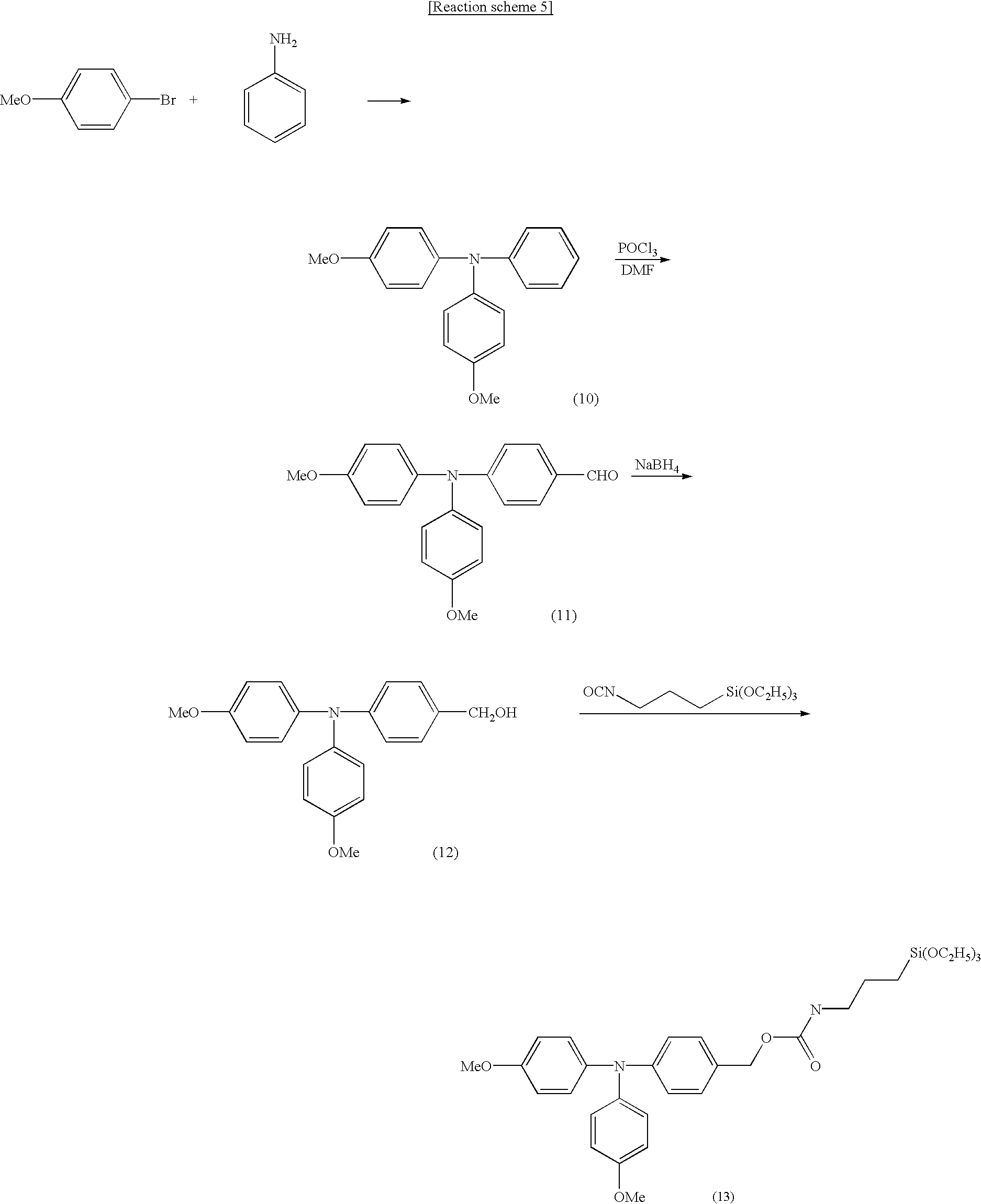
- Synthesis of Bis(4-methoxyphenyl)phenylamine
- 9 g of aniline and 9 g of 4-methoxy-bromobenzene was dissolved in toluene (250 mL). NaO-t-Bu (5.3 g), Pd 2(dba)3 (0.4 g), and P(t-Bu)3 (0.5 g) were added to the above solution at room temperature. The reaction mixture was stirred at 100° C. for 12 hours under N2. After cooling to room temperature, the mixture was quenched by adding aqueous ammonia (300 mL). An organic layer was separated from the reactant solution using methylene chloride and dried using magnesium sulfate. Then, methylene chloride was removed under reduced pressure and recrystallized using methylene chloride and hexane, yielding 65% of a white solid. Data of NMR spectra and elemental analysis confirmed that the product had the same structure as the compound (10) in the reaction scheme 5.
- Synthesis of 4-bis(4′-methoxyphenyl)aminobenzaldehyde
- 30 mL of dimethylformaldehyde (DMF) was put into a 250 mL flask, cooled to 0° C. and 3.8 mL of POCl 3 was slowly added thereto. Then, 10 g of compound (10) was added to the resultant mixture and heated to 70° C. for 5 hours. The reaction container was cooled to room temperature and then a reactant solution was poured into ice water. Subsequently, 40 g of sodium acetate trihydrate was put for neutralization and then an organic layer was separated with methylenechloride. The obtained organic layer was dried using magnesium sulfate and methylenechloride was removed under reduced pressure, yielding a product. The product was recrystallized using methanol and a light yellow solid was finally obtained, yielding 73% of a desired product. Data of NMR spectra confirmed that the product had the same structure as 4-(bis(4′-methoxyphenyl)amino)benzaldehyde, that is, the compound (11) in the reaction scheme 5.
- Synthesis of [4-bis(4′-methoxyphenyl)aminophenyl]methanol
- The compound (11) obtained in Example 4-2, that is, 4-(bis(4′-methoxyphenyl)amino)benzaldehyde (5.1 g) was dissolved in 50 mL of ethanol and a solution prepared by dissolving 0.29 g of NaBH 4 in 0.1 M aqueous solution of NaOH (15 mL) was slowly added thereto. The reactant solution was reacted at room temperature for 4 hours. An organic layer was separated from the reactant solution using methylene chloride and recrystallized in a methylene chloride/hexane solvent, yielding 92% of a white solid. Data of NMR spectra confirmed that the product had the same structure as the compound (12) in the reaction scheme 5.
- Synthesis of MeO2-TPA-CONH-silane
- The compound obtained in Example 4-3, that is, [4-bis(4′-methoxyphenyl)aminophenyl]methanol (12.0 g, 36.3 mmol), was dissolved in 30 mL of dimethylformamide, 10.3 mL (72.6 mmol) of triethylamine was added thereto and stirred for 30 minutes. Then, 3.5 mL (33 mmol) of (3-isocyanatopropyle)triethoxysilane was added and reacted at 70° C. for 48 hours. The resultant was concentrated under reduced pressure and then separated by column chromatography. The separated product was recrystallized using methylene chloride and hexane, yielding 40% of a white solid. Data of NMR spectra and elemental analysis confirmed that the product had the same structure as the compound (13) in the reaction scheme 5, that is, MeO2-TPA-CONH-silane.
- Preparation of a Self-assembled Monolayer (1)
- Silicon wafers each having a <100> crystal growth orientation were washed with chloroform and water and treated in a solution having concentrated sulfuric acid and H 2O2 (35%) mixed in a volume ratio of 7:3 at 120° C. for 10 minutes. Thereafter, the resultant structures were added to a solution having NH4OH (35%), H2O2 and H2O mixed in a volume ratio of 1:1:5 and treated at 80° C. for 20 minutes. Then, the wafers were washed with water and dried with nitrogen gas. Each of the prepared wafers was immersed in toluene solutions having the compound synthesized in Example 1-3, that is, TPA-CONH-silane, and the compound synthesized in Example 2-2, that is, Car-CONH-silane, dissolved in a concentration of 1 mM, respectively, and reacted at room temperature for 24 hours. After completion of the reaction, the silicon wafers were washed with an acetone solvent and finally washed with water. Then, the washed wafers were dried with dry nitrogen gas, thereby forming a self-assembled monolayer comprised of the compound synthesized in Example 1-3, that is, TPA-CONH-silane, and the compound synthesized in Example 2-2, that is, Car-CONH-silane, on each silicon wafer
- Preparation of a Self-assembled Monolayer (2)
- ITO substrates were washed with chloroform and water and added to a solution having NH 4OH (35%), H2O2 and H2O mixed in a volume ratio of 1:1:5 and treated at 80° C. for 20 minutes. Then, the ITO substrates were finally washed with water and dried with dry nitrogen gas.
- Each of the prepared substrates was immersed in a toluene solution having the compound synthesized in Example 1-3, that is, TPA-CONH-silane, and the compound synthesized in Example 2-2, that is, Car-CONH-silane, dissolved in a concentration of 1 mM, respectively, and reacted at room temperature for 24 hours. After completion of the reaction, the ITO substrates were washed with an acetone solvent and finally washed with water. Then, the washed wafers were dried with dry nitrogen gas, thereby forming a self-assembled monolayer comprised of the compound synthesized in Example 1-3, that is, TPA-CONH-silane, and the compound synthesized in Example 2-2, that is, Car-CONH-silane, on each ITO substrate.
- Evaluation of Self-assembled Monolayers (1)
- Thickness of Self-assembled Monolayers
- The thicknesses of the self-assembled monolayers prepared in Example 3 were measured using an ellipsometer. The measurement results showed that the self-assembled monolayer comprised of the compound synthesized in Example 1-3, that is, TPA-CONH-silane, and the self-assembled monolayer comprised of the compound synthesized in Example 2-2, that is, Car-CONH-silane, had thicknesses in the range of 10 to 20 Å.
- Evaluation of Self-assembled Monolayers (2)
- XPS Spectrum of Self-assembled Monolayers
- Elements of the self-assembled monolayers formed on the silicon wafers and the ITO substrates were analyzed using X-ray Photo-electron Spectroscopy (XPS). The self-assembled monolayer comprised of the compound synthesized in Example 1-3, that is, TPA-CONH-silane, was used for analysis. FIG. 3 shows an XPS spectrum of the self-assembled monolayer comprised of TPA-CONH-silane formed on a silicon wafer, and FIG. 4 shows an XPS spectrum of the self-assembled monolayer comprised of TPA-CONH-silane formed on an ITO substrate. FIGS. 3 and 4 show observation results of peaks indicating characteristics of the respective self-assembled monolayers with respect to C, N and Si, respectively.
- Evaluation of Self-assembled Monolayers (3)
- Surface Roughness of Self-assembled Monolayers
- The surface roughness of a TPA-CONH-silane self-assembled monolayer formed on a silicon wafer was analyzed using atomic force microscope (AFM), and the results thereof are shown in FIG. 5. The analysis results of FIG. 5 were evaluated by a root mean square (RMS) method, resulting in roughness of 1.21 Å.
- In Comparison Example, the surface roughness of a silicon wafer without a self-assembled monolayer was analyzed, and the results thereof are shown in FIG. 6. The analysis results of FIG. 6 were evaluated by RMS, resulting in roughness of 1.03 Å.
- FIGS. 5 and 6 show that substantially the same roughness was observed before and after forming the TPA-CONH-silane self-assembled monolayer on a silicon wafer.
- Evaluation of Self-assembled Monolayer (4)
- Work Function of Self-assembled Monolayer
- The work function of each of a TPA-CONH-silane self-assembled monolayer and a Car-CONH-silane self-assembled monolayer was measured using an atmospheric type ultraviolet spectrometer (model AC-2; Riken Keiki). As a result, the work function of 5.3 eV, higher than that of ITO substrate surface, i.e., 4.8 eV, was obtained in both the two self-assembled monolayers. This confirms that the TPA-CONH-silane self-assembled monolayer and the Car-CONH-silane self-assembled monolayer can smoothly perform electron injection between the electron transporting layer and the ITO substrate.
- Evaluation of Self-assembled Monolayer (5)
- Contact Angle of Water at Self-assembled Monolayer
- In order to evaluate hydrophilicity and hydrophobicity of a self-assembled monolayer comprising the compound according to the present invention, water contact angles were measured on the TPA-CONH-silane self-assembled monolayer and the Car-CONH-silane self-assembled monolayer formed on silicon wafers, respectively. Also, in Comparison Example, the water contact angle was measured for the silicon wafer surface without a self-assembled monolayer. As a result, whereas the water contact angle for the silicon wafer surface without a self-assembled monolayer was less than 15 degrees, the water contact angles for the silicon wafer surfaces with the TPA-CONH-silane self-assembled monolayer and the Car-CONH-silane self-assembled monolayer were approximately 77 and 74 degrees, respectively. In other words, the resulting surfaces with the TPA-CONH-silane self-assembled monolayer and the Car-CONH-silane self-assembled monolayer formed on the silicon wafers were more hydrophobic than the silicon wafer surface, confirming that these surfaces could provide for good adhesion to another layer materials.
- Evaluation of Self-assembled Monolayer (6)
- Thermal Stability of Organic Film Formed on Self-assembled Monolayer
- In order to evaluate thermal stability of an organic film formed on a self-assembled monolayer comprising the compound according to the present invention, the self-assembled monolayer comprising the compound according to the present invention was formed on an ITO substrate, and a triphenyldiamine (TPD) layer as a hole transporting layer was then formed thereon to a thickness of 500 Å by vacuum deposition. Here, samples of self-assembled monolayers formed of TPA-CONH-silane and Car-CONH-silane were prepared, respectively. Also, comparative samples of TPD layers directly formed on ITO substrates without a self-assembled monolayer to a thickness of 500 Å, were prepared.
- The thus-prepared samples were heat-treated under inert gas (nitrogen) atmosphere at 150° C. for 3 hours. After heat treatment, scanning electron microscope (SEM) analysis performed on TPD layers of the respective samples showed that the TPD layers formed on the respective ITO substrates with the TPA-CONH-silane self-assembled monolayer and the Car-CONH-silane self-assembled monolayer maintained the same shape, without any change, before and after heat treatment. However, in the case where the ITO substrate without a self-assembled monolayer, the observation result showed that the TPD layer could not maintain its original shape but an island-shaped domain was discontinuously formed. These findings confirm that adhesiveness between an ITO substrate and a TPD layer is increased by forming a self-assembled monolayer comprising the compound according to the present invention therebetween.
- Manufacture of Organic Electroluminescent Device
- The compounds prepared in Examples 1-3 and 2-2 were used in manufacturing organic electroluminescent devices. In detail, referring to FIG. 7, a self-assembled
monolayer 20 was formed on aglass substrate 10 havingtransparent electrode 12 made of ITO in the same manner as in Example 4. monolayers of the TPA-CONH-silane and the Car-CONH-silane synthesized in Examples 1-3 and 2-2 were used as the self-assembledmonolayer 20, and the thickness thereof was in the range of 10 to 20 Å. Thereafter, a hole transporting/injectinglayer 22, alight emitting layer 24, an electron transport/injection layer 26 and ametal electrode 28 are sequentially formed on the self-assembledmonolayer 20. In this embodiment, an approximately 500 Å thick TPD layer was formed as the hole transporting/injectinglayer 22, and an approximately 600 Å thick A lQ3 (tris(8-quinolinolato) aluminum ) layer was formed as the hole transporting/injectinglayer 2. In other words, the electron transporting/injectinglayer 26 made of AlQ3 also serves as the light-emittinglayer 24. The AlQ3 layer was formed by evaporation performed at a pressure of 10−6 torr. As themetal electrode 28, an Al layer was formed to a thickness of approximately 700 Å. Also, in this embodiment, a buffer layer (not shown) made of LiF was interposed between the AlQ3 layer, i.e., the electron transporting/injectinglayer 26, and themetal electrode 28 to a thickness of approximately 20 Å. - Although only particular embodiments have been described, the
substrate 10 may be formed of polycarbonate, polyimide, polyethyleneterephthalate or polyethylenenaphthalate, in addition to glass. Also, thetransparent electrode 12 constitutes an anode of an organic electroluminescent device, and may be formed of indium oxide, tin oxide, zinc oxide or mixtures thereof mixed in an appropriate ratio according to desired transmittance and conductivity, in addition to the above-referenced ITO. Further, thetransparent electrode 12 may be formed by sputtering. The self-assembledmonolayer 20 is formed for the purpose of improving adhesiveness between thetransparent electrode 12 and the hole transporting/injectinglayer 22 while improving the capabilities of transporting and injecting holes, and may be formed of a single compound or a mixture of two or more compounds. - Evaluation of Organic Electroluminescent Device (1)
- Electrical Properties
- The electrical properties of the organic electroluminescent device prepared in Example 11 were evaluated. FIG. 8 shows the evaluation results of electrical properties of organic electroluminescent devices with the self-assembled
monolayer 20 formed of the TPA-CONH-silane compound prepared in Example 1-3, marked by , and the Car-CONH-silane compound prepared in Example 2-2, marked by ▴, respectively, and without the self-assembledmonolayer 20 as in Comparison Example, marked by . As shown in FIG. 8, a high current density can be acquired even at a low voltage, by forming the self-assembledmonolayer 20 between thetransparent electrode 12 and the hole transporting/injectinglayer 22, thereby improving the electrical properties of the organic electroluminescent device. In particular, in the case where the self-assembledmonolayer 20 is formed of the Car-CONH-silane prepared in Example 2-2, very good electrical properties were obtained. - Evaluation of Organic Electroluminescent Device (2)
- Luminance
- The electroluminescent properties of the organic electroluminescent device prepared in Example 11 were evaluated. FIG. 9 shows the evaluation results of applied voltage-dependent luminance of organic electroluminescent devices with the self-assembled
monolayer 20 formed of the TPA-CONH-silane compound prepared in Example 1-3, marked by , and the Car-CONH-silane compound prepared in Example 2-2, marked by ▴, respectively, and without the self-assembledmonolayer 20 as in Comparison Example, marked by . As shown in FIG. 9, high luminance can be acquired even at a low voltage, by forming the self-assembledmonolayer 20 between thetransparent electrode 12 and the hole transporting/injectinglayer 22, thereby improving the electrical properties of the organic electroluminescent device. In particular, in the case where the self-assembledmonolayer 20 is formed of the Car-CONH-silane prepared in Example 2-2, very high luminous efficiency, that is, approximately twice the maximum luminance of that in Comparison Example, was obtained. - Evaluation of Organic Electroluminescent Device (3)
- Performance
- The performances of the organic electroluminescent devices prepared in Examples 12 and 13 according to the present invention, as shown in FIGS. 8 and 9, were evaluated, and the results thereof are shown in FIGS. 10 and 11. Referring to FIGS. 10 and 11, the organic electroluminescent devices with the self-assembled
monolayer 20 formed between thetransparent electrode 12 and the hole transporting/injectinglayer 22, are higher in performance than the organic electroluminescent device without the self-assembledmonolayer 20 as in Comparison Example. - As described above, the compounds according to the present invention siloxane compounds including molecular components having excellent hole transporting capability. Thus, a self-assembled monolayer having a uniform thickness can be formed on the substrate surface using the compound of the present invention. The surface roughness of the thus-formed self-assembled monolayer can be maintained at a level of the substrate itself. Also, the organic EL device according to the present invention has the self-assembled monolayer interposed between hole transporting/injecting layers comprised of a transparent electrode and an organic thin film. Thus, adhesion between the transparent electrode and the organic thin film can be enhanced, and holes can be smoothly transported or injected from the transparent electrode serving as an anode to the organic thin film by varying the work function at the surface of the transparent electrode. Also, excellent stability with respect to heat and time, excellent electrical characteristics and high luminous efficiency can be attained.
- Although the invention has been described with reference to particular preferred embodiments, it is to be understood that the invention is not limited to the particulars disclosed and extends to all equivalents within the scope of the claims.
Claims (15)


Applications Claiming Priority (2)
| Application Number | Priority Date | Filing Date | Title |
|---|---|---|---|
| KR10-2001-0055046A KR100438888B1 (en) | 2001-09-07 | 2001-09-07 | Compounds capable of transporting/injecting hole and organic electroluminescence device having self-assembled monolayer comprising the same |
| KR2001-55046 | 2001-09-07 |
Publications (2)
| Publication Number | Publication Date |
|---|---|
| US20030087127A1 true US20030087127A1 (en) | 2003-05-08 |
| US6878468B2 US6878468B2 (en) | 2005-04-12 |
Family
ID=19714035
Family Applications (1)
| Application Number | Title | Priority Date | Filing Date |
|---|---|---|---|
| US10/201,214 Expired - Fee Related US6878468B2 (en) | 2001-09-07 | 2002-07-22 | Compounds capable of transporting/injecting hole and organic electroluminescent device having self-assembled monolayer comprising the same |
Country Status (2)
| Country | Link |
|---|---|
| US (1) | US6878468B2 (en) |
| KR (1) | KR100438888B1 (en) |
Cited By (13)
| Publication number | Priority date | Publication date | Assignee | Title |
|---|---|---|---|---|
| US20050025994A1 (en) * | 2003-07-29 | 2005-02-03 | Junichi Hanna | Organic electroluminescent element and method for producing the same |
| US20050282308A1 (en) * | 2004-06-22 | 2005-12-22 | Albrecht Uhlig | Organic electroluminescent display device and method of producing the same |
| WO2006116584A2 (en) * | 2005-04-27 | 2006-11-02 | Dynamic Organic Light, Inc. | Light emitting polymer devices using self-assembled monolayer structures |
| JP2006321752A (en) * | 2005-05-19 | 2006-11-30 | Ricoh Co Ltd | New silyl compound, electrophotographic photoreceptor given by using the same, image forming device, and process cartridge for image forming device |
| JP2009512187A (en) * | 2005-10-07 | 2009-03-19 | ダウ コーニング コーポレイシヨン | Electrophosphorescent organic light-emitting diodes formed using solvent-soluble materials |
| US7811624B1 (en) * | 2004-12-30 | 2010-10-12 | Dupont Displays, Inc. | Self-assembled layers for electronic devices |
| JP2010228957A (en) * | 2009-03-26 | 2010-10-14 | Fujifilm Corp | Inorganic material, device and organic electroluminescent device |
| US8853070B2 (en) * | 2012-04-13 | 2014-10-07 | Oti Lumionics Inc. | Functionalization of a substrate |
| EP2872125A4 (en) * | 2012-07-10 | 2016-02-24 | Dana Farber Cancer Inst Inc | Anti-proliferative compounds and uses thereof |
| US9698386B2 (en) | 2012-04-13 | 2017-07-04 | Oti Lumionics Inc. | Functionalization of a substrate |
| US9864251B2 (en) | 2015-02-25 | 2018-01-09 | Electronics And Telecommunications Research Institute | Color changeable device |
| CN110003089A (en) * | 2019-03-04 | 2019-07-12 | 陕西科技大学 | A kind of 3- methylol -9- substituted carbazole and preparation method thereof |
| CN116400068A (en) * | 2023-02-13 | 2023-07-07 | 泉州圣源警用侦察设备有限公司 | Reagent for revealing potential biological trace containing DNA and revealing method |
Families Citing this family (7)
| Publication number | Priority date | Publication date | Assignee | Title |
|---|---|---|---|---|
| KR100783366B1 (en) * | 2004-12-14 | 2007-12-07 | 한국전자통신연구원 | Organic light emitting diodes containing self assembled monolayer and method for preparing the same |
| KR20080018576A (en) * | 2006-08-25 | 2008-02-28 | 삼성전자주식회사 | Method of ohmic contact for organic active layer and method of manufacturing flat panel display, and organic thin film transistor display and organic light emitting diode display |
| US7759677B2 (en) | 2006-09-05 | 2010-07-20 | Electronics And Telecommunications Research Institute | Molecular electronic device including organic dielectric thin film and method of fabricating the same |
| DE102008006374B4 (en) * | 2007-09-27 | 2018-12-06 | Osram Oled Gmbh | Electric organic component and method for its production |
| DE102009012163A1 (en) * | 2009-03-06 | 2010-09-09 | Siemens Aktiengesellschaft | Monolayers of organic compounds on metal oxide surfaces or oxide-containing metal surfaces and component produced therewith based on organic electronics |
| KR102512533B1 (en) * | 2016-02-23 | 2023-03-22 | 삼성디스플레이 주식회사 | Organic light emitting device |
| KR102477550B1 (en) * | 2020-07-09 | 2022-12-15 | 연세대학교 산학협력단 | Ferroelectric Luminescent Self-Assembly compound and organic electronic device comprising the same |
Citations (6)
| Publication number | Priority date | Publication date | Assignee | Title |
|---|---|---|---|---|
| US5688961A (en) * | 1995-11-06 | 1997-11-18 | Dow Corning Asia, Ltd. | Method of manufacturing a silicon-type charge transporting material |
| US5834100A (en) * | 1996-06-25 | 1998-11-10 | Northwestern University | Organic light-emitting dioddes and methods for assembly and emission control |
| US6323355B2 (en) * | 1998-04-30 | 2001-11-27 | Fuji Photo Film Co., Ltd. | Specific vinylsilane compound, organic luminous element containing the same, and method for producing vinylsilane compound |
| US6339221B1 (en) * | 1999-02-01 | 2002-01-15 | Delphi Technologies, Inc. | Ferroelectric thermometry and pyrometry by active operation |
| US6503831B2 (en) * | 1997-10-14 | 2003-01-07 | Patterning Technologies Limited | Method of forming an electronic device |
| US6558819B1 (en) * | 1999-08-20 | 2003-05-06 | Fuji Photo Film Co., Ltd. | Arylsilane compound, light emitting device material and light emitting device by using the same |
Family Cites Families (5)
| Publication number | Priority date | Publication date | Assignee | Title |
|---|---|---|---|---|
| TW558561B (en) * | 1997-07-22 | 2003-10-21 | Sumitomo Chemical Co | Hole transporting polymer and organic electroluminescence device using the same |
| WO1999007028A1 (en) | 1997-07-31 | 1999-02-11 | Ecole Polytechnique Federale De Lausanne | Electroluminescent device |
| JP3314732B2 (en) * | 1998-03-06 | 2002-08-12 | 富士ゼロックス株式会社 | Electrophotographic photoreceptor and electrophotographic image forming apparatus |
| KR100317284B1 (en) * | 1999-04-30 | 2001-12-22 | 구자홍 | Organic Electroluminescent Device |
| KR100379442B1 (en) * | 2000-12-12 | 2003-04-11 | 엘지전자 주식회사 | organic electroluminescence device |
-
2001
- 2001-09-07 KR KR10-2001-0055046A patent/KR100438888B1/en not_active IP Right Cessation
-
2002
- 2002-07-22 US US10/201,214 patent/US6878468B2/en not_active Expired - Fee Related
Patent Citations (6)
| Publication number | Priority date | Publication date | Assignee | Title |
|---|---|---|---|---|
| US5688961A (en) * | 1995-11-06 | 1997-11-18 | Dow Corning Asia, Ltd. | Method of manufacturing a silicon-type charge transporting material |
| US5834100A (en) * | 1996-06-25 | 1998-11-10 | Northwestern University | Organic light-emitting dioddes and methods for assembly and emission control |
| US6503831B2 (en) * | 1997-10-14 | 2003-01-07 | Patterning Technologies Limited | Method of forming an electronic device |
| US6323355B2 (en) * | 1998-04-30 | 2001-11-27 | Fuji Photo Film Co., Ltd. | Specific vinylsilane compound, organic luminous element containing the same, and method for producing vinylsilane compound |
| US6339221B1 (en) * | 1999-02-01 | 2002-01-15 | Delphi Technologies, Inc. | Ferroelectric thermometry and pyrometry by active operation |
| US6558819B1 (en) * | 1999-08-20 | 2003-05-06 | Fuji Photo Film Co., Ltd. | Arylsilane compound, light emitting device material and light emitting device by using the same |
Cited By (22)
| Publication number | Priority date | Publication date | Assignee | Title |
|---|---|---|---|---|
| US20050025994A1 (en) * | 2003-07-29 | 2005-02-03 | Junichi Hanna | Organic electroluminescent element and method for producing the same |
| US20050282308A1 (en) * | 2004-06-22 | 2005-12-22 | Albrecht Uhlig | Organic electroluminescent display device and method of producing the same |
| US7811624B1 (en) * | 2004-12-30 | 2010-10-12 | Dupont Displays, Inc. | Self-assembled layers for electronic devices |
| WO2006116584A2 (en) * | 2005-04-27 | 2006-11-02 | Dynamic Organic Light, Inc. | Light emitting polymer devices using self-assembled monolayer structures |
| WO2006116584A3 (en) * | 2005-04-27 | 2007-01-18 | Dynamic Organic Light Inc | Light emitting polymer devices using self-assembled monolayer structures |
| JP4618678B2 (en) * | 2005-05-19 | 2011-01-26 | 株式会社リコー | Novel silyl compound, electrophotographic photosensitive member using the same, image forming apparatus, and process cartridge for image forming apparatus |
| JP2006321752A (en) * | 2005-05-19 | 2006-11-30 | Ricoh Co Ltd | New silyl compound, electrophotographic photoreceptor given by using the same, image forming device, and process cartridge for image forming device |
| JP2009512187A (en) * | 2005-10-07 | 2009-03-19 | ダウ コーニング コーポレイシヨン | Electrophosphorescent organic light-emitting diodes formed using solvent-soluble materials |
| EP2412674A1 (en) * | 2009-03-26 | 2012-02-01 | FUJIFILM Corporation | Inorganic material, device, and organic electroluminescent element |
| KR101616154B1 (en) | 2009-03-26 | 2016-04-27 | 유디씨 아일랜드 리미티드 | Inorganic material, device, and organic electroluminescent element |
| JP2010228957A (en) * | 2009-03-26 | 2010-10-14 | Fujifilm Corp | Inorganic material, device and organic electroluminescent device |
| EP2412674A4 (en) * | 2009-03-26 | 2013-03-27 | Udc Ireland Ltd | Inorganic material, device, and organic electroluminescent element |
| KR20110133566A (en) * | 2009-03-26 | 2011-12-13 | 후지필름 가부시키가이샤 | Inorganic material, device, and organic electroluminescent element |
| US9698386B2 (en) | 2012-04-13 | 2017-07-04 | Oti Lumionics Inc. | Functionalization of a substrate |
| US8853070B2 (en) * | 2012-04-13 | 2014-10-07 | Oti Lumionics Inc. | Functionalization of a substrate |
| US9853233B2 (en) | 2012-04-13 | 2017-12-26 | Oti Lumionics Inc. | Functionalization of a substrate |
| US10290833B2 (en) | 2012-04-13 | 2019-05-14 | Oti Lumionics Inc. | Functionalization of a substrate |
| EP2872125A4 (en) * | 2012-07-10 | 2016-02-24 | Dana Farber Cancer Inst Inc | Anti-proliferative compounds and uses thereof |
| US9969679B2 (en) | 2012-07-10 | 2018-05-15 | Dana-Farber Cancer Institute, Inc. | Anti-proliferative compounds and uses thereof |
| US9864251B2 (en) | 2015-02-25 | 2018-01-09 | Electronics And Telecommunications Research Institute | Color changeable device |
| CN110003089A (en) * | 2019-03-04 | 2019-07-12 | 陕西科技大学 | A kind of 3- methylol -9- substituted carbazole and preparation method thereof |
| CN116400068A (en) * | 2023-02-13 | 2023-07-07 | 泉州圣源警用侦察设备有限公司 | Reagent for revealing potential biological trace containing DNA and revealing method |
Also Published As
| Publication number | Publication date |
|---|---|
| US6878468B2 (en) | 2005-04-12 |
| KR100438888B1 (en) | 2004-07-02 |
| KR20030021674A (en) | 2003-03-15 |
Similar Documents
| Publication | Publication Date | Title |
|---|---|---|
| US6878468B2 (en) | Compounds capable of transporting/injecting hole and organic electroluminescent device having self-assembled monolayer comprising the same | |
| Lee et al. | Modification of an ITO anode with a hole-transporting SAM for improved OLED device characteristics | |
| US6451461B2 (en) | Hole transporting compounds having good thermal stability for organic electroluminescent device and method for production thereof | |
| JP3939579B2 (en) | White electroluminescent polymer compound and organic electroluminescent device using the same | |
| US7345301B2 (en) | Mixtures of matrix materials and organic semiconductors capable of emission, use of the same and electronic components containing said mixtures | |
| JP4868099B2 (en) | Electroluminescent device | |
| EP1859656B1 (en) | Organometallic complexes | |
| US7781761B2 (en) | Substituted anthracenes and electronic devices containing the substituted anthracenes | |
| US20100308754A1 (en) | Hole Transport Polymer for Use in Electronic Devices | |
| US8575392B2 (en) | Charge-transporting varnish | |
| EP0439627A1 (en) | Organic electroluminescent element | |
| KR101153587B1 (en) | Arylamine compound and organic electroluminescent device | |
| US20070077450A1 (en) | Conjugated compounds containing triarylamine structural elements, and their use | |
| US6277504B1 (en) | EL assembly based on tertiary amines, Alq3 derivatives or mixtures soluble in alcohol and polymeric binders | |
| US7666525B2 (en) | Organic electroluminescent device comprising a polymer layer containing a polymide having triphenylamine derivative unit | |
| US20130015431A1 (en) | Lithium metal quinolates and process for preparation thereof as good emitting, interface materials as well as n-type dopent for organic electronic devices | |
| US20060134538A1 (en) | Aromatic chalcogen compounds and their use | |
| KR20080104344A (en) | Novel 1,3,5-tris(diarylamino)benzenes and use thereof | |
| JP2000178236A (en) | New hole-transfer diamine substance and organic electroluminescent element containing the substance | |
| KR0154995B1 (en) | Thin film electroluminescence device | |
| US20060091359A1 (en) | Organic light emitting compounds for a blue-light electroluminescent device | |
| WO2017080446A1 (en) | Purely electronic organic semiconductor diode component | |
| KR100783366B1 (en) | Organic light emitting diodes containing self assembled monolayer and method for preparing the same | |
| JP5891055B2 (en) | Arylamine compound and organic electroluminescence device | |
| US7026061B2 (en) | Organic electroluminescent material and organic electroluminescent element by using the same |
Legal Events
| Date | Code | Title | Description |
|---|---|---|---|
| AS | Assignment |
Owner name: ELECTRONICS AND TELECOMMUNICATIONS RESEARCH INSTIT Free format text: ASSIGNMENT OF ASSIGNORS INTEREST;ASSIGNORS:LEE, JEONG-IK;CHU, HYE-YONG;LEE, HYO-YOUNG;AND OTHERS;REEL/FRAME:013136/0941 Effective date: 20020702 |
|
| FEPP | Fee payment procedure |
Free format text: PAYOR NUMBER ASSIGNED (ORIGINAL EVENT CODE: ASPN); ENTITY STATUS OF PATENT OWNER: SMALL ENTITY |
|
| AS | Assignment |
Owner name: ELECTRONICS AND TELECOMMUNICATIONS RESEARCH INSTIT Free format text: ASSIGNMENT OF ASSIGNORS INTEREST;ASSIGNORS:LEE, JEONG-IK;CHU, HYE-YONG;LEE, HYO-YOUNG;AND OTHERS;REEL/FRAME:017109/0034 Effective date: 20020702 Owner name: KOREA ADVANCED INSTITUTE OF SCIENCE AND TECHNOLOGY Free format text: ASSIGNMENT OF ASSIGNORS INTEREST;ASSIGNORS:LEE, JEONG-IK;CHU, HYE-YONG;LEE, HYO-YOUNG;AND OTHERS;REEL/FRAME:017109/0034 Effective date: 20020702 |
|
| FPAY | Fee payment |
Year of fee payment: 4 |
|
| FEPP | Fee payment procedure |
Free format text: PAYER NUMBER DE-ASSIGNED (ORIGINAL EVENT CODE: RMPN); ENTITY STATUS OF PATENT OWNER: SMALL ENTITY Free format text: PAYOR NUMBER ASSIGNED (ORIGINAL EVENT CODE: ASPN); ENTITY STATUS OF PATENT OWNER: SMALL ENTITY |
|
| FPAY | Fee payment |
Year of fee payment: 8 |
|
| REMI | Maintenance fee reminder mailed | ||
| LAPS | Lapse for failure to pay maintenance fees | ||
| STCH | Information on status: patent discontinuation |
Free format text: PATENT EXPIRED DUE TO NONPAYMENT OF MAINTENANCE FEES UNDER 37 CFR 1.362 |
|
| FP | Lapsed due to failure to pay maintenance fee |
Effective date: 20170412 |