US20020172766A1 - Low dielectric constant thin films and chemical vapor deposition method of making same - Google Patents
Low dielectric constant thin films and chemical vapor deposition method of making same Download PDFInfo
- Publication number
- US20020172766A1 US20020172766A1 US09/811,106 US81110601A US2002172766A1 US 20020172766 A1 US20020172766 A1 US 20020172766A1 US 81110601 A US81110601 A US 81110601A US 2002172766 A1 US2002172766 A1 US 2002172766A1
- Authority
- US
- United States
- Prior art keywords
- group
- ligand
- alkyl
- cvd process
- process according
- Prior art date
- Legal status (The legal status is an assumption and is not a legal conclusion. Google has not performed a legal analysis and makes no representation as to the accuracy of the status listed.)
- Abandoned
Links
- 0 [1*][Si]([2*])([2*])[2*] Chemical compound [1*][Si]([2*])([2*])[2*] 0.000 description 21
Images


Classifications
-
- C—CHEMISTRY; METALLURGY
- C23—COATING METALLIC MATERIAL; COATING MATERIAL WITH METALLIC MATERIAL; CHEMICAL SURFACE TREATMENT; DIFFUSION TREATMENT OF METALLIC MATERIAL; COATING BY VACUUM EVAPORATION, BY SPUTTERING, BY ION IMPLANTATION OR BY CHEMICAL VAPOUR DEPOSITION, IN GENERAL; INHIBITING CORROSION OF METALLIC MATERIAL OR INCRUSTATION IN GENERAL
- C23C—COATING METALLIC MATERIAL; COATING MATERIAL WITH METALLIC MATERIAL; SURFACE TREATMENT OF METALLIC MATERIAL BY DIFFUSION INTO THE SURFACE, BY CHEMICAL CONVERSION OR SUBSTITUTION; COATING BY VACUUM EVAPORATION, BY SPUTTERING, BY ION IMPLANTATION OR BY CHEMICAL VAPOUR DEPOSITION, IN GENERAL
- C23C16/00—Chemical coating by decomposition of gaseous compounds, without leaving reaction products of surface material in the coating, i.e. chemical vapour deposition [CVD] processes
- C23C16/22—Chemical coating by decomposition of gaseous compounds, without leaving reaction products of surface material in the coating, i.e. chemical vapour deposition [CVD] processes characterised by the deposition of inorganic material, other than metallic material
- C23C16/30—Deposition of compounds, mixtures or solid solutions, e.g. borides, carbides, nitrides
-
- C—CHEMISTRY; METALLURGY
- C07—ORGANIC CHEMISTRY
- C07F—ACYCLIC, CARBOCYCLIC OR HETEROCYCLIC COMPOUNDS CONTAINING ELEMENTS OTHER THAN CARBON, HYDROGEN, HALOGEN, OXYGEN, NITROGEN, SULFUR, SELENIUM OR TELLURIUM
- C07F7/00—Compounds containing elements of Groups 4 or 14 of the Periodic System
- C07F7/02—Silicon compounds
- C07F7/08—Compounds having one or more C—Si linkages
- C07F7/0834—Compounds having one or more O-Si linkage
- C07F7/0838—Compounds with one or more Si-O-Si sequences
-
- C—CHEMISTRY; METALLURGY
- C07—ORGANIC CHEMISTRY
- C07F—ACYCLIC, CARBOCYCLIC OR HETEROCYCLIC COMPOUNDS CONTAINING ELEMENTS OTHER THAN CARBON, HYDROGEN, HALOGEN, OXYGEN, NITROGEN, SULFUR, SELENIUM OR TELLURIUM
- C07F7/00—Compounds containing elements of Groups 4 or 14 of the Periodic System
- C07F7/02—Silicon compounds
- C07F7/08—Compounds having one or more C—Si linkages
- C07F7/18—Compounds having one or more C—Si linkages as well as one or more C—O—Si linkages
- C07F7/1896—Compounds having one or more Si-O-acyl linkages
Definitions
- the present invention relates to a process for forming low dielectric constant thin films useful as insulating materials in microelectronic device structures. More particularly, the present invention is directed to a CVD process for forming porous, low-dielectric constant, SiOC thin films having dielectric constants of less than 2.7.
- low dielectric constant (K) materials advantageously lowers power consumption, reduces cross talk, and shortens signal delay for closely spaced conductors through reduction of both nodal and interconnect line capacitances.
- Dielectric materials, which exhibit low dielectric constants, are critical in the development path toward faster and more power efficient microelectronics.
- SiO 2 Silicon oxide
- SiO 2 with a dielectric constant of approximately 4
- the interconnect delay associated with SiO 2 is a limiting factor in advanced integrated circuits.
- One approach to lowering the dielectric constant of the SiO 2 insulating layer is by incorporation of carbon. Carbon incorporation from between 15-20%, reduces the dielectric constant to as low as 2.7, in part due to the substitution of the highly polarized Si—O link by Si—C, (i.e., Nakano, et al., “Effects of Si—C Bond Content on Film Properties of Organic Spin-on Glass” J. Electrochem. Soc., Vol. 142, No. 4, April 1995, pp. 1303-1307).
- TCTS 2,4,6,8-tetramethylcyclotetrasiloxane
- a second approach to lowering the dielectric constant is to use porous, low-density, silicon oxide materials in which a fraction of the bulk volume of the SiO 2 film contains air, which has a dielectric constant of 1.
- silica aerogels are porous solids having dielectric constants in the range of from about 2.0 to 1.01 (i.e., Lu, et al., “Low dielectric Constant Materials-Synthesis and Applications in Microelectronics”, Mat. Res. Soc. Sym. Proc., April 17-19, San Francisco, Calif., 1995, pp. 267-272).
- the silica aerogels are prepared by sol-gel techniques, which are not well adapted for high-throughput semiconductor processing environments, due to long processing times, saturated alcohol atmospheres, and, in many applications, high pressures for supercritical solvent extraction.
- Chemical vapor deposition is the thin film deposition method of choice for large-scale fabrication of microelectronic device structures, and the semiconductor manufacturing industry has extensive expertise in its use.
- the present invention is directed to the formation of a porous, low dielectric constant SiOC thin film by a process which comprises chemical vapor depositing on a substrate an organosilicon thin film, containing cleavable organic functional groups that upon activation rearrange and cleave as highly volatile liquid and/or gaseous species, to produce a porous, SiOC, thin film having a dielectric constant of less than 3.0.
- the term “low dielectric constant” refers to a dielectric material with a value of the dielectric constant, k, below 3.0 as measured at a frequency of 1 mega-Hertz.
- the term “thin film” refers to a film having a thickness in the range of from about 1000 ⁇ to about 2 ⁇ m and the term “SiOC” refers to a thin film composition comprising from about 1 to about 40 atomic percent silicon, preferably from about 20 to 40 percent silicon, from about 1 to about 60 atomic percent oxygen, preferably from about 40 to 60 percent oxygen and from about 1 to about 20 atomic percent carbon and preferably from 5 to 17 percent carbon.
- the present invention relates to an organosilicon precursor useful for producing porous, low-dielectric constant, SiOC thin films, wherein the organosilicon precursor comprises at least one cleavable, organic functional group that upon activation rearranges, decomposes and cleaves as a highly volatile liquid or gaseous by-product.
- cleavable refers to an organic functional group, bonded to the silicon atom of the organosilicon precursor that when activated (i.e., thermal, light or plasma enhanced), rearranges, decomposes and/or is liberated as a volatile liquid or gaseous by-product, i.e. CO 2 .
- the organosilicon precursor is di(formato)dimethylsilane, a novel composition useful for the deposition of low dielectric constant thin films, comprising the formula:
- the present invention relates to a method of synthesizing di(formato)dimethylsilane by a method comprising:
- M 1 is selected from the group consisting of Na (sodium), K (potassium) and Ag (silver).
- the present invention relates to a CVD process for producing a porous, low dielectric constant, SiOC thin film on a substrate, from at least one organosilicon precursor comprising at least one cleavable, organic functional group that upon activation, rearranges, decomposes and cleaves as a highly volatile liquid or gaseous by-product.
- the present invention relates to a porous, dielectric, SiOC thin film produced by the process as described hereinabove.
- FIG. 1 shows a simplified schematic representation of a process system for forming a low k dielectric film on a substrate in accordance with one embodiment of the invention.
- FIG. 2 shows a simplified schematic representation of a process system for forming a low k dielectric thin film on a substrate in accordance with a further embodiment of the invention.
- FIG. 3 shows a mass spectroscopic analysis of di(formato)dimethylsilane.
- the present invention contemplates the use of organosilicon precursors for CVD formation of porous low dielectric constant thin films, in which the composition contains at least one cleavable organic group that upon activation, rearranges, decomposes and/or cleaves as a highly volatile liquid or gaseous by product.
- the organosilicon precursor compositions useful in the invention include compounds having at least one substituent that upon activation, rearranges, decomposes rearranges and/or cleaves as a highly volatile liquid or gaseous by-product.
- the invention relates to organosilicon precursors for producing porous, low dielectric constant, SiOC thin films, wherein the composition of the organosilicon precursor comprises at least one cleavable organic group that upon activation, rearranges, decomposes and/or cleaves as a highly volatile liquid or gaseous by product.
- Embodiment 2 relates to organosilicon precursors useful for producing porous, low dielectric constant, SiOC thin films, comprising the general formula:
- R 1 is a cleavable organic functional group, selected from the group consisting of C 2 to C 6 alkene, C 2 to C 6 alkyne, C 3 to C 4 allyl, C 1 to C 6 alkyl, C 1 to C 6 perfluoroalkyl; ligand X as described hereinbelow, and ligand Y as described hereinbelow; and
- each of R 2 is same or different and each of R 2 is selected from the group consisting of H, ligand X as described hereinbelow, ligand Y as described hereinbelow, C 2 to C 6 alkene, C 2 to C 6 alkyne, C 3 to C 4 allyl, C 1 to C 6 alkyl, C 1 to C 6 perfluoroalkyl, C 1 to C 6 alkoxy, aryl, perfluoroaryl and C 2 to C 6 alkylsilane; and
- R 1 is a cleavable organic functional group, selected from the group consisting of C 2 to C 6 alkene, C 2 to C 6 alkyne, C 3 to C 4 allyl, C 1 to C 6 alkyl, C 1 to C 6 perfluoroalkyl; ligand X as described hereinbelow, and ligand Y as described hereinbelow; and
- each of R 2 is same or different and each of R 2 is selected from the group consisting of H, ligand X as described hereinbelow, ligand Y as described hereinbelow, C 2 to C 6 alkene, C 2 to C 6 alkyne, C 3 to C 4 allyl, C 1 to C 6 alkyl, C 1 to C 6 perfluoroalkyl, C 1 to C 6 alkoxy, aryl, perfluoroaryl and C 2 to C 6 alkylsilane.
- the invention relates to organosilicon precursors useful for producing porous, low dielectric constant, SiOC thin films, wherein the organosilicon precursor comprises a composition containing at least one alkyl group and at least one organic functional group that upon activation, rearranges, decomposes and/or cleaves as a highly volatile liquid or gaseous by product.
- Embodiment 4 relates to organosilicon precursors for producing porous, low dielectric constant, SiOC thin films, comprising the general formula:
- ligand X is a cleavable organic functional group as depicted in Formula 3;
- R 3 is selected from the group consisting of: H, C 1 to C 6 alkyl, C 1 to C 6 perfluoroalkyl, C 1 to C 6 carboxylate, aryl and perfluoroaryl;
- R is selected from the group consisting of: C 1 to C 4 alkyl and C 1 to C 4 perfluoroalkyl;
- each of R 2 is same or different and each of R 2 is selected from the group consisting of H, ligand X as described hereinabove, ligand Y as described hereinbelow, C 2 to C 6 alkene, C 2 to C 6 alkyne, C 3 to C 4 allyl, C 1 to C 4 alkyl, C 1 to C 4 perfluoroalkyl, C 1 to C 6 alkoxy, aryl, perfluoroaryl and C 2 to C 6 alkylsilane;
- R 4 is a cleavable organic functional group selected from the group consisting of: C 2 to C 6 alkene, and C 2 to C 6 alkyne, C 3 to C 4 allyl, C 1 to C 6 alkyl, C 1 to C 6 perfluoroalkyl; C 1 to C 6 alkylsilane, and ligand Y as described hereinbelow;
- R is selected from the group consisting of: C 1 to C 4 alkyl and C 1 to C 4 perfluoroalkyl;
- each of R 2 is same or different and each of R 2 is selected from the group consisting of H, ligand X as described hereinabove, ligand Y as described hereinbelow, C 2 to C 6 alkene, C 2 to C 6 alkyne, C 3 to C 4 allyl, C 1 to C 4 alkyl, C 1 to C 4 perfluoroalkyl, C 1 to C 6 alkoxy, aryl, perfluoroaryl and C 2 to C 6 alkylsilane;
- ligand Y is a cleavable organic functional group as depicted in Formula 3;
- R 3 is selected from the group consisting of: H, C 1 to C 6 alkyl, C 1 to C 6 perfluoroalkyl aryl; perfluoroaryl and C 1 to C 6 carboxylate;
- R is selected from the group consisting of: C 1 to C 4 alkyl and C 1 to C 4 perfluoroalkyl;
- each of R 2 is same or different and each of R 2 is selected from the group consisting of H, ligand X as described hereinabove, ligand Y as described hereinbelow, C 2 to C 6 alkene, C 2 to C 6 alkyne, C 3 to C 4 allyl, C 1 to C 4 alkyl, C 1 to C 4 perfluoroalkyl, C 1 to C 6 alkoxy, aryl, perfluoroaryl and C 2 to C 6 alkylsilane;
- R 4 is a cleavable organic functional group selected from the group consisting of: C 2 to C 6 alkene, and C 2 to C 6 alkyne, C 3 to C 4 allyl, C 1 to C 6 alkyl, C 1 to C 6 perfluoroalkyl; C 1 to C 6 alkylsilane, and ligand Y as described hereinabove;
- each of R is same or different and each of R is selected from the group consisting of: C 1 to C 4 alkyl and C 1 to C 4 perfluoroalkyl; and
- each of R 2 is same or different and each of R 2 is selected from the group consisting of H, ligand X as described hereinabove, ligand Y as described hereinabove, C 2 to C 6 alkene, C 2 to C 6 alkyne, C 3 to C 4 allyl, C 1 to C 4 alkyl, C 1 to C 4 perfluoroalkyl, C 1 to C 6 alkoxy, aryl, perfluoroaryl and C 2 to C 6 alkylsilane; and
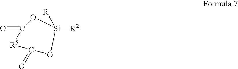
- R 5 is optional and may be selected from the group consisting of C 1 to C 2 alkyl
- R is selected from the group consisting of: C 1 to C 4 alkyl and C 1 to C 4 perfluoroalkyl;
- R 2 is selected from the group consisting of H, ligand X as described hereinabove, ligand Y as described hereinabove, C 2 to C 6 alkene, C 2 to C 6 alkyne, C 3 to C 4 allyl, C 1 to C 4 alkyl, C 1 to C 4 perfluoroalkyl, C 1 to C 6 alkoxy, aryl, perfluoroaryl and C 2 to C 6 alkylsilane.
- Examples of the volatile by-products produced by the activation step of the present invention include but are not limited to: Cleavable functional group Volatile by-product carboxylate CO, HCOH, CO 2 dicarboxylate CO, HOCH, CO 2 alkene alkynes, hydrocarbons alkyne hydrocarbons alkyl alkene benzylate CO 2 , phenyl, benzene
- Embodiment 5 the present invention relates to di(formato)dimethylsilane, a novel organosilicon precursor composition useful for producing low dielectric constant thin films, comprising the formula:
- organosilicon compositions of the invention are usefully employed to form low dielectric constant thin films on substrates by chemical vapor deposition. More particularly diformatodimethylsilane is useful for producing porous, low dielectric constant, SiOC thin films.
- the present invention relates to a method of synthesizing di(formato)dimethylsilane by a method comprising:
- M 1 is selected from the group consisting of: Na(sodium), K (potassium) and Ag (silver).
- organosilicon precursors useful in the present invention include but are not limited to:
- organosilicon precursors of the present invention are available commercially through Gelest, Inc., a leading supplier of silanes, or such precursors may be readily synthesized using methods that are well known in the art.
- the present invention relates to a chemical vapor deposition (CVD) process and more preferably a plasma enhanced chemical vapor deposition (PECVD) process for forming a low dielectric constant thin film on a substrate, including the steps of:
- the organosilicon thin film of Embodiment 6 retains between 1 and 100 percent of the cleavable, organic functional groups, more preferably the organosilicon thin film retains between about 25 to 100 percent of the cleavable organic functional groups and most preferably, the organosilicon thin film retains between about 50 to 100 percent of the cleavable organic functional groups.
- Embodiment 7 the present invention relates to a CVD process and more preferably a PECVD process, for forming low dielectric constant thin films on a substrate, including the steps of:
- the organosilicon thin film of Embodiment 7 retains between 1 to 100 percent of the cleavable, organic functional groups and between 1 to 100 percent of the alkyl groups; more preferably the organosilicon thin film retains between about 25 to 100 percent of the cleavable organic functional groups and between about 25 to 100 percent of the alkyl groups; and most preferably, the organosilicon thin film retains between about 50 to 100 percent of the cleavable organic functional groups and between about 50 to 100 percent of the alkyl groups.
- the annealing step of Embodiments 6 and 7 is carried out at a temperature in the range of from about 100° C. to about 400° C., optionally in the presence of an oxidizing or reducing gas, for a length of time and under conditions sufficient to effect the removal of the cleavable, organic functional groups and optionally a portion of the alkyl groups (if present) to produce a porous, SiOC thin film having a dielectric constant of less than 3.0.
- the annealing step of Embodiments 6 and 7 may further comprise plasma enhanced conditions, at a temperature in the range of from about 100 to about 400° C., optionally in the presence of an oxidizing or reducing gas, for a length of time and under conditions sufficient to effect the removal of the volatile organic groups and optionally a portion of the alkyl groups, to produce a porous, SiOC thin film having a dielectric constant of less than 3.0.
- an organosilicon precursor vapor comprising from about 1 to about 100% by volume of an organosilicon composition as described in Embodiments 1-4, and from about 0 to about 99% by volume of an inert carrier gas, based on the total volume of organosilicon precursor vapor and the inert carrier gas, is subjected to chemical vapor deposition (CVD) conditions, preferably plasma enhanced chemical vapor deposition conditions, in a chamber containing a substrate, so that the precursor composition in vapor or plasma form is contacted with the substrate in the CVD chamber to deposit thereon, a dense SiOC thin film comprising cleavable organic functional groups.
- CVD chemical vapor deposition
- the present invention relates to an organosilicon precursor vapor comprising from about 1 to about 100% by volume of an organosilicon composition as described in Embodiments 3-4, and from about 0 to about 99% by volume of an inert carrier gas, based on the total volume of organosilicon precursor vapor and the inert carrier gas, is subjected to chemical vapor deposition (CVD) conditions, preferably plasma enhanced chemical vapor deposition conditions, in a chamber containing a substrate, so that the precursor composition in vapor or plasma form is contacted with the substrate in the CVD chamber to deposit thereon, a dense SiOC thin film comprising alkyl groups and cleavable organic functional groups.
- CVD chemical vapor deposition
- an organosilicon precursor vapor comprising from about 1 to about 100% by volume of an organosilicon composition as described in Embodiments 1-4, from about 0 to about 99% by volume of an inert carrier gas, and from about 1 to about 99% by volume of at least one co-reactant, based on the total volume of organosilicon precursor vapor, inert carrier gas and co-reactant, is subjected to chemical vapor deposition (CVD) conditions, preferably plasma enhanced chemical vapor deposition conditions in a plasma chamber containing a substrate, so that the precursor composition in vapor or plasma form is contacted with the substrate in the CVD chamber to deposit thereon, a dense SiOC thin film comprising cleavable organic functional groups thereon.
- CVD chemical vapor deposition
- an organosilicon precursor vapor comprising from about 1 to about 100% by volume of an organosilicon composition as described in Embodiments 3-4, and from about 0 to about 99% by volume of an inert carrier gas and from about 1 to about 99% by volume of at least one co-reactant, based on the total volume of organosilicon precursor vapor, inert carrier gas and co-reactant, is subjected to chemical vapor deposition (CVD) conditions, preferably plasma enhanced chemical vapor deposition conditions in a plasma chamber containing a substrate, so that the precursor composition in vapor or plasma form is contacted with the substrate in the CVD chamber to deposit thereon, a dense SiOC thin film comprising alkyl groups and cleavable organic functional groups thereon.
- CVD chemical vapor deposition
- the organosilicon compounds may optionally be used in combination with other co-reactants, i.e., other organosilicon precursors of the present invention, other organosilicon precursors, or reactive gases i.e. CO 2 , ethylene, acetylene, N 2 O, O 2 , H 2 and mixtures thereof.
- other co-reactants i.e., other organosilicon precursors of the present invention, other organosilicon precursors, or reactive gases i.e. CO 2 , ethylene, acetylene, N 2 O, O 2 , H 2 and mixtures thereof.
- the inert carrier gas in the processes described hereinabove may be of any suitable type, i.e., argon, helium, etc. or a compressible gas or liquid, i.e., CO 2 .
- the processes of Embodiments 6 and 7, may further include subjecting at least one organosilicon precursor as described hereinabove in Embodiments 1-4 to chemical vapor deposition (CVD) conditions in a CVD chamber containing a substrate, so that the precursor composition is deposited in such a form as to retain a portion of the original cleavable organic functional groups, wherein the CVD conditions include temperature in the chamber in a range of from about 50° C. to about 400° C. and more preferably in a range of from about 250° C. to about 350° C., and a chamber pressure in a range of from about 500 mTorr to about 10 Torr, more preferably the chamber pressure is set to about 4 Torr.
- CVD chemical vapor deposition
- the processes of Embodiments 7, may further include subjecting at least one organosilicon precursor as described hereinabove in Embodiments 3 and 4 to chemical vapor deposition (CVD) conditions in a CVD chamber containing a substrate, so that the precursor composition is deposited in such a form as to retain a portion of the original alkyl and cleavable organic functional groups, wherein the CVD conditions include temperature in the chamber in a range of from about 50° C. to about 400° C. and more preferably in a range of from about 250° C. to about 350° C., and a chamber pressure in a range of from about 500 mTorr to about 10 Torr, more preferably the chamber pressure is set to about 4 Torr.
- CVD chemical vapor deposition
- the plasma may be generated from single or mixed frequency RF power.
- the plasma source may comprise a high frequency, radio frequency (HFRF) plasma source component generating power in a range of from about 75 W to about 200 W at a frequency of about 13.56 MHz or a low frequency radio frequency (LFRF) plasma source component generating power in a range from about 5 W and 75 W at a frequency of about 350 kHz and/or combinations thereof.
- HFRF radio frequency
- LFRF low frequency radio frequency
- the plasma is maintained for a period of time sufficient to deposit the dense SiOC thin film having retained therein between 1 to 100 percent of the original alkyl groups and between 1 and 100 percent of the cleavable organic functional groups.
- the dense SiOC thin film retains between 50 to 100 percent of the original alkyl groups and between 50 to 100 percent of the original cleavable organic functional groups.
- the deposition process of Embodiments 6-10 is tuned with single frequency or dual frequency operating simultaneously to yield a dense SiOC thin film wherein between 1 and 100 percent of the alkyl groups and between 1 and 100 percent of the cleavable organic functional groups are retained in the deposited film.
- the dense SiOC film formed in Embodiment 6 or Embodiment 7 is post annealed in a furnace, at a temperature in the range of from about 100° C. to about 400° C., optionally in the presence of an oxidizing or reducing gas, for a length of time and under conditions sufficient to effect the removal of at least a portion of the cleavable organic functional groups and a desired portion of the alkyl groups to produce a porous, low dielectric constant, SiOC thin film.
- the dense SiOC thin film may be optionally annealed at a gradually increasing temperature profile to effect the rearrangement and volatilization of the cleavable organic groups.
- the dense SiOC thin film is annealed at a temperature of about 400° C.
- the post-annealing step as serves to activate the cleavable organic groups retained in the dense SiOC thin film in such a way as to effect the rearrangement and/or decomposition of the cleavable organic groups to form volatile organic liquid or gaseous by-products.
- a portion of the alkyl groups in the dense SiOC thin film retains the carbon, resulting in Si—C bonds.
- the final result is a micro-porous, low dielectric constant SiOC thin film.
- the post-annealing step activates the cleavable functional groups by way of a rearrangement process that results in a volatile organic species and forms uniformly distributed pores throughout the thin film.
- the carbon concentration of the micro-porous, SiOC thin film may be tailored to give optimum carbon levels that result in a material with a lower dielectric constant and increased hardness, by varying process conditions that are well known to those skilled in the art.
- the post-annealing step occurs under plasma-enhanced or oxygen assisted plasma conditions.
- the annealing step may further comprise: co-reactants, such as CO 2 ; oxidizing gases, such as O 2, O 3 , N 2 O or NO; reducing gases such as H 2 or NH 3 ; inert gases, such as He or Ar; and/or combinations thereof.
- co-reactants such as CO 2 ; oxidizing gases, such as O 2, O 3 , N 2 O or NO; reducing gases such as H 2 or NH 3 ; inert gases, such as He or Ar; and/or combinations thereof.
- the micro-porous, low dielectric constant, SiOC thin film of the instant invention comprises between 5 and 99 percent porosity, more preferably between 5 and 80 percent porosity and most preferably between 5 and 70 percent porosity.
- the porosity of the micro-porous, SiOC thin film may be tailored to give optimum porosity levels that result is a material with a lower dielectric constant, by varying the percentage of cleavable organic functional groups in the organosilicon precursor(s) and by varying process conditions that are well known to those skilled in the art.
- porosity refers to that fraction of the low dielectric constant thin film that comprises air and includes molecular sized pores in the range of from about 5 to 20 nm, mesopores (between molecules) of less than 150 nm and micropores (within the particle), of less than 2 nm.
- the micro-porous, low dielectric constant, SiOC thin film comprises between 1 and 20 percent carbon, more preferably between 1 and 15 percent carbon and most preferably between 1 and 10 percent carbon.
- the dielectric constant of the porous SiOC thin film produced by any one of the aforementioned embodiments is less than 3.0, more preferably the dielectric constant of the porous SiOC thin film is less than 2.0 and most preferably the dielectric constant of the porous SiOC thin film is less than 1.5.
- Specific CVD conditions and more particularly PECVD conditions are readily determinable for a given application by empirically varying the process conditions (e.g., pressure, temperature, flow rate, relative proportions of the organosilicon precursor gas and inert carrier gas in the composition, etc.) and developing correlation to the film properties produced in the process.
- the conditions of the process as disclosed herein are monitored to retain alkyl and cleavable organic groups in the dense SiOC film.
- FIG. 1 is a schematic representation of a process system 10 for forming a low k dielectric film
- a source 12 of organosilicon precursor(s) is joined by line 18 to disperser (i.e., showerhead or aerosol nozzle) 28 in CVD reactor 24 .
- the CVD reactor may be constructed and arranged to carry out CVD involving thermal dissociation of the precursor vapor to deposit the desired SiOC film on the substrate 34 mounted on susceptor 30 heated by heating element 32 .
- the CVD reactor may be constructed and arranged for carrying out plasma-enhanced CVD, by ionization of the precursor gas mixture.
- a source 16 of carrier gases is also provided, joined by line 22 to the disperser 28 in CVD reactor 24 .
- the disperser 28 may comprise a showerhead nozzle, jet or the like which functions to receive and mix the feed streams from the respective sources 12 , 14 and 16 , to form a gaseous precursor mixture which then is flowed toward the substrate 34 on the heated susceptor 30 .
- the substrate 34 may be a silicon wafer or other substrate element and material, on which the low k dielectric film is deposited.
- the streams may be combined in a mixing vessel or chamber upstream of the CVD reactor 24 .
- a plasma generator unit may be provided as part of or upstream of the CVD reactor 24 .
- the feed streams from sources 12 and 16 may be monitored in lines 18 and 22 , respectively, by means of suitable monitoring devices (not shown in FIG. 1), and the flow rates of the respective streams may be independently controlled (by means such as mass flow controllers, pumps, blowers, flow control valves, regulators, restricted flow orifice elements, etc., also not shown) to provide a combined precursor feed stream having a desired compositional character.
- the precursor formulations of the invention may be employed in any suitable chemical vapor deposition system to form corresponding thin films on a substrate or microelectronic device precursor structure as a dielectric layer thereon.
- the CVD system may for example comprise a liquid delivery CVD system, a bubbler-based CVD system, or a CVD system of any other suitable type.
- Suitable liquid delivery CVD systems include those disclosed in Kirlin et al. U.S. Pat. No. 5,204,134; Kirlin et al. U.S. Pat. No. 5,536,323; and Kirlin et al. U.S. Pat. No. 5,711,816.
- the source liquid may comprise the source reagent compound(s) or complex(es) per se, if the compound(s) or complex(es) are in the liquid phase at ambient temperature (e.g., room temperature, 25° C.) or otherwise at the supply temperature from which the source reagent is rapidly heated and vaporized to form precursor vapor for the CVD process.
- ambient temperature e.g., room temperature, 25° C.
- the source reagent compound or complex is a solid at ambient or the supply temperature
- such compound(s) or complex(es) can be dissolved or suspended in a compatible solvent medium to provide a liquid phase composition that can be submitted to rapid heating and vaporization to form precursor vapor for the CVD process.
- the precursor vapor resulting from the vaporization then is transported, optionally in combination with a carrier gas (e.g., He, Ar, H 2 , O 2 , etc.), to the chemical vapor deposition reactor where the vapor is contacted with a substrate at elevated temperature to deposit material from the vapor phase onto the substrate or semiconductor device precursor structure positioned in the CVD reactor.
- a carrier gas e.g., He, Ar, H 2 , O 2 , etc.
- reagent delivery systems such as bubblers and heated vessels can be employed.
- bubbler-based delivery systems an inert carrier gas is bubbled through the precursor composition to provide a resulting fluid stream that is wholly or partially saturated with the vapor of the precursor composition, for flow to the CVD tool.
- any method that delivers the precursor composition to the CVD tool may be usefully employed.
- the present invention relates to a porous, dielectric, SiOC thin film produced by the process as described hereinabove in Embodiments 6 and 7.
- the present invention relates to a porous dielectric thin film produced by the process as described hereinabove in Embodiments 6 and 7, wherein the dielectric constant of the thin film is less than 2.
- the present invention relates to a porous dielectric thin film produced by a process as described hereinabove in Embodiments 6 and 7, wherein the dielectric constant of the thin film is less than 1.5.
- FIG. 2 is a schematic representation of a process system 10 for forming a low k dielectric film on a substrate in accordance with a preferred embodiment of the invention.
- Di(formato)dimethylsilane is delivered into a PECVD deposition chamber 38 as a chemical vapor.
- the di(formato)dimethylsilane may be delivered with a carrier gas.
- the chemical vapor is obtained either by vapor draw or by direct liquid injection of liquid into a vaporizer, which is heated to an elevated temperature.
- the deposition process is carried out on a substrate 40 , typically a silicon wafer, at a temperature in a range of from about 100-400° C. in the presence of a single frequency or dual frequency ( 42 ) plasma activation.
- Film properties and deposition parameters are monitored as a function of plasma power, reactor pressure, oxygen to precursor ratio, and deposition temperature.
- the deposition process is monitored to obtain a film with the desired composition of Si x O y C z .
- the process is optimized to retain the highest percentage of the functional groups and a desired percentage of the alkyl groups in the film.
- the process involves annealing at higher temperatures and or by additional plasma activation.
- the functional groups are cleaved as volatile gaseous or high vapor pressure liquids that are removed continuously.
- some of the methyl groups are retained in the deposited film.
- the formato group is a cleavable functional group used to generate micro porosity in the resulting thin film.
- the volatile products generated by rearrangement and/or decomposition of the formato ligand include but are not limited CO, CO 2 , and CH 2 O.
- the cleavable formato ligand contains a ⁇ -hydrogen that under conditions as described herein, undergoes a rearrangement process that results in the formation of cleavable volatile products, i.e., CO, CO 2 , and CH 2 O, with high vapor pressure.
- FIG. 3 shows a mass spectroscopic analysis of di(formato)dimethylsilane (CHOO) 2 Si(CH 3 ) 2 .
- the mass spectroscopic analysis evidences the fragmentation pattern of the molecule under mass spec conditions.
- a strong molecular ion peak at m/e 133 reveals loss of one CH 3 group with subsequent ⁇ -rearrangement of the formato hydrogens and loss of two CO groups as shown by molecular fragments at m/e 105 and m/e 77 .
- the mass specification fragmentation pattern evidences the inherent tendency of the formato groups to rearrange and cleave as volatile by-products.
Abstract
A CVD process for producing low-dielectric constant, SiOC thin films using organosilicon precursor compositions having at least one alkyl group and at least one cleavable organic functional group that when activated rearranges and cleaves as a highly volatile liquid or gaseous by-product. In a first step, a dense SiOC thin film is CVD deposited from the organosilicon precursor having at least one alkyl group and at least one cleavable organic functional group, having retained therein at least a portion of the alkyl and cleavable organic functional groups. In a second step, the dense SiOC thin film is post annealed to effectively remove the volatile liquid or gaseous by-products, resulting in a porous low-dielectric constant SiOC thin film. The porous, low dielectric constant, SiOC thin films are useful as insulating layers in microelectronic device structures. Preferred porous, low-dielectric SiOC thin films are produced using di(formato)dimethylsilane as the organosilicon precursor.
Description
- The present invention relates to a process for forming low dielectric constant thin films useful as insulating materials in microelectronic device structures. More particularly, the present invention is directed to a CVD process for forming porous, low-dielectric constant, SiOC thin films having dielectric constants of less than 2.7.
- As the need for integrated circuits for semiconductor devices having higher performance and greater functionality increases, device feature geometries continue to decrease. As device geometries become smaller, the dielectric constant of an insulating material used between conducting paths becomes an increasingly important factor in device performance.
- As device dimensions shrink to less than 0.25 μm, propagation delay, cross-talk noise and power dissipation due to resistance-capacitance (RC) coupling become significant due to increased wiring capacitance, especially interline capacitance between the metal lines on the same level. These factors all depend critically on the dielectric constant of the separating insulator.
- The use of low dielectric constant (K) materials advantageously lowers power consumption, reduces cross talk, and shortens signal delay for closely spaced conductors through reduction of both nodal and interconnect line capacitances. Dielectric materials, which exhibit low dielectric constants, are critical in the development path toward faster and more power efficient microelectronics.
- Silicon oxide (SiO 2), with a dielectric constant of approximately 4, has long been used in integrated circuits as the primary insulating material. However, the interconnect delay associated with SiO2 is a limiting factor in advanced integrated circuits.
- In order to produce faster and more power efficient microelectronics with smaller device geometries, insulating materials having dielectric constants of less than 3.0 are necessary.
- One approach to lowering the dielectric constant of the SiO 2 insulating layer is by incorporation of carbon. Carbon incorporation from between 15-20%, reduces the dielectric constant to as low as 2.7, in part due to the substitution of the highly polarized Si—O link by Si—C, (i.e., Nakano, et al., “Effects of Si—C Bond Content on Film Properties of Organic Spin-on Glass” J. Electrochem. Soc., Vol. 142, No. 4, April 1995, pp. 1303-1307).
- Alkyl silanes, alkoxy silanes and cyclic-siloxanes such as 2,4,6,8-tetramethylcyclotetrasiloxane (TMCTS) are being evaluated aggressively for obtaining low dielectric constant (k) thin-films as interlayer dielectrics in an integrated circuit by a PECVD approach. The resulting films formed when using these precursors give dense SiOC containing films, having dielectric constants in the range of from about 2.7 to 3.0.
- A second approach to lowering the dielectric constant is to use porous, low-density, silicon oxide materials in which a fraction of the bulk volume of the SiO 2 film contains air, which has a dielectric constant of 1.
- As an example, silica aerogels are porous solids having dielectric constants in the range of from about 2.0 to 1.01 (i.e., Lu, et al., “Low dielectric Constant Materials-Synthesis and Applications in Microelectronics”, Mat. Res. Soc. Sym. Proc., April 17-19, San Francisco, Calif., 1995, pp. 267-272). The silica aerogels are prepared by sol-gel techniques, which are not well adapted for high-throughput semiconductor processing environments, due to long processing times, saturated alcohol atmospheres, and, in many applications, high pressures for supercritical solvent extraction.
- Chemical vapor deposition (CVD) is the thin film deposition method of choice for large-scale fabrication of microelectronic device structures, and the semiconductor manufacturing industry has extensive expertise in its use.
- It would therefore be a significant advance in the art to provide a high throughput CVD process, for producing low dielectric constant, silica thin films on a substrate, having dielectric constants less than 3.0.
- It therefore is an object of the present invention to provide such process for producing low dielectric constant silica thin films on a substrate, having dielectric constants less than 3.0.
- Other objects and advantages of the present invention will be more fully apparent from the ensuing disclosure and appended claims.
- The present invention is directed to the formation of a porous, low dielectric constant SiOC thin film by a process which comprises chemical vapor depositing on a substrate an organosilicon thin film, containing cleavable organic functional groups that upon activation rearrange and cleave as highly volatile liquid and/or gaseous species, to produce a porous, SiOC, thin film having a dielectric constant of less than 3.0.
- As used herein, the term “low dielectric constant” refers to a dielectric material with a value of the dielectric constant, k, below 3.0 as measured at a frequency of 1 mega-Hertz. The term “thin film” refers to a film having a thickness in the range of from about 1000 Å to about 2 μm and the term “SiOC” refers to a thin film composition comprising from about 1 to about 40 atomic percent silicon, preferably from about 20 to 40 percent silicon, from about 1 to about 60 atomic percent oxygen, preferably from about 40 to 60 percent oxygen and from about 1 to about 20 atomic percent carbon and preferably from 5 to 17 percent carbon.
- In one aspect, the present invention relates to an organosilicon precursor useful for producing porous, low-dielectric constant, SiOC thin films, wherein the organosilicon precursor comprises at least one cleavable, organic functional group that upon activation rearranges, decomposes and cleaves as a highly volatile liquid or gaseous by-product.
- As used herein, the term cleavable refers to an organic functional group, bonded to the silicon atom of the organosilicon precursor that when activated (i.e., thermal, light or plasma enhanced), rearranges, decomposes and/or is liberated as a volatile liquid or gaseous by-product, i.e. CO 2.
- In a preferred aspect of the invention the organosilicon precursor is di(formato)dimethylsilane, a novel composition useful for the deposition of low dielectric constant thin films, comprising the formula:
- (CH3)2Si(OOCH)2
- In a further aspect, the present invention relates to a method of synthesizing di(formato)dimethylsilane by a method comprising:
- 2M1(OOCH)+(CH3)2SiCl2→(CH3)2Si(OOCH)2+2M1Cl
- wherein M 1 is selected from the group consisting of Na (sodium), K (potassium) and Ag (silver). In a further aspect the present invention relates to a CVD process for producing a porous, low dielectric constant, SiOC thin film on a substrate, from at least one organosilicon precursor comprising at least one cleavable, organic functional group that upon activation, rearranges, decomposes and cleaves as a highly volatile liquid or gaseous by-product.
- In yet another aspect, the present invention relates to a porous, dielectric, SiOC thin film produced by the process as described hereinabove.
- FIG. 1 shows a simplified schematic representation of a process system for forming a low k dielectric film on a substrate in accordance with one embodiment of the invention.
- FIG. 2 shows a simplified schematic representation of a process system for forming a low k dielectric thin film on a substrate in accordance with a further embodiment of the invention.
- FIG. 3 shows a mass spectroscopic analysis of di(formato)dimethylsilane.
- The present invention contemplates the use of organosilicon precursors for CVD formation of porous low dielectric constant thin films, in which the composition contains at least one cleavable organic group that upon activation, rearranges, decomposes and/or cleaves as a highly volatile liquid or gaseous by product.
- The organosilicon precursor compositions useful in the invention include compounds having at least one substituent that upon activation, rearranges, decomposes rearranges and/or cleaves as a highly volatile liquid or gaseous by-product.
- In one embodiment (hereafter referred to as Embodiment 1) the invention relates to organosilicon precursors for producing porous, low dielectric constant, SiOC thin films, wherein the composition of the organosilicon precursor comprises at least one cleavable organic group that upon activation, rearranges, decomposes and/or cleaves as a highly volatile liquid or gaseous by product.
- In a further embodiment (hereafter referred to as Embodiment 2) the invention relates to organosilicon precursors useful for producing porous, low dielectric constant, SiOC thin films, comprising the general formula:

- wherein
- R 1 is a cleavable organic functional group, selected from the group consisting of C2 to C6 alkene, C2 to C6 alkyne, C3 to C4 allyl, C1 to C6 alkyl, C1 to C6 perfluoroalkyl; ligand X as described hereinbelow, and ligand Y as described hereinbelow; and
- each of R 2 is same or different and each of R2 is selected from the group consisting of H, ligand X as described hereinbelow, ligand Y as described hereinbelow, C2 to C6 alkene, C2 to C6 alkyne, C3 to C4 allyl, C1 to C6 alkyl, C1 to C6 perfluoroalkyl, C1 to C6 alkoxy, aryl, perfluoroaryl and C2 to C6 alkylsilane; and

- wherein
- R 1 is a cleavable organic functional group, selected from the group consisting of C2 to C6 alkene, C2 to C6 alkyne, C3 to C4 allyl, C1 to C6 alkyl, C1 to C6 perfluoroalkyl; ligand X as described hereinbelow, and ligand Y as described hereinbelow; and
- each of R 2 is same or different and each of R2 is selected from the group consisting of H, ligand X as described hereinbelow, ligand Y as described hereinbelow, C2 to C6 alkene, C2 to C6 alkyne, C3 to C4 allyl, C1 to C6 alkyl, C1 to C6 perfluoroalkyl, C1 to C6 alkoxy, aryl, perfluoroaryl and C2 to C6 alkylsilane.
- In a further embodiment (hereafter referred to as Embodiment 3) the invention relates to organosilicon precursors useful for producing porous, low dielectric constant, SiOC thin films, wherein the organosilicon precursor comprises a composition containing at least one alkyl group and at least one organic functional group that upon activation, rearranges, decomposes and/or cleaves as a highly volatile liquid or gaseous by product.
- In a further embodiment (hereafter referred to as Embodiment 4) the invention relates to organosilicon precursors for producing porous, low dielectric constant, SiOC thin films, comprising the general formula:

- wherein
- ligand X is a cleavable organic functional group as depicted in Formula 3;
- R 3 is selected from the group consisting of: H, C1 to C6 alkyl, C1 to C6 perfluoroalkyl, C1 to C6 carboxylate, aryl and perfluoroaryl;
- R is selected from the group consisting of: C 1 to C4 alkyl and C1 to C4 perfluoroalkyl; and
- each of R 2 is same or different and each of R2 is selected from the group consisting of H, ligand X as described hereinabove, ligand Y as described hereinbelow, C2 to C6 alkene, C2 to C6 alkyne, C3 to C4 allyl, C1 to C4 alkyl, C1 to C4 perfluoroalkyl, C1 to C6 alkoxy, aryl, perfluoroaryl and C2 to C6 alkylsilane;

- wherein
- R 4 is a cleavable organic functional group selected from the group consisting of: C2 to C6 alkene, and C2 to C6 alkyne, C3 to C4 allyl, C1 to C6 alkyl, C1 to C6 perfluoroalkyl; C1 to C6 alkylsilane, and ligand Y as described hereinbelow;
- R is selected from the group consisting of: C 1 to C4 alkyl and C1 to C4 perfluoroalkyl; and
- each of R 2 is same or different and each of R2 is selected from the group consisting of H, ligand X as described hereinabove, ligand Y as described hereinbelow, C2 to C6 alkene, C2 to C6 alkyne, C3 to C4 allyl, C1 to C4 alkyl, C1 to C4 perfluoroalkyl, C1 to C6 alkoxy, aryl, perfluoroaryl and C2 to C6 alkylsilane;

- wherein
- ligand Y is a cleavable organic functional group as depicted in Formula 3;
- R 3 is selected from the group consisting of: H, C1 to C6 alkyl, C1 to C6 perfluoroalkyl aryl; perfluoroaryl and C1 to C6 carboxylate;,
- R is selected from the group consisting of: C 1 to C4 alkyl and C1 to C4 perfluoroalkyl; and
- each of R 2 is same or different and each of R2 is selected from the group consisting of H, ligand X as described hereinabove, ligand Y as described hereinbelow, C2 to C6 alkene, C2 to C6 alkyne, C3 to C4 allyl, C1 to C4 alkyl, C1 to C4 perfluoroalkyl, C1 to C6 alkoxy, aryl, perfluoroaryl and C2 to C6 alkylsilane;

- wherein
- R 4 is a cleavable organic functional group selected from the group consisting of: C2 to C6 alkene, and C2 to C6 alkyne, C3 to C4 allyl, C1 to C6 alkyl, C1 to C6 perfluoroalkyl; C1 to C6 alkylsilane, and ligand Y as described hereinabove;
- each of R is same or different and each of R is selected from the group consisting of: C 1 to C4 alkyl and C1 to C4 perfluoroalkyl; and
- each of R 2 is same or different and each of R2 is selected from the group consisting of H, ligand X as described hereinabove, ligand Y as described hereinabove, C2 to C6 alkene, C2 to C6 alkyne, C3 to C4 allyl, C1 to C4 alkyl, C1 to C4 perfluoroalkyl, C1 to C6 alkoxy, aryl, perfluoroaryl and C2 to C6 alkylsilane; and

- wherein
- R 5 is optional and may be selected from the group consisting of C1 to C2 alkyl;
- R is selected from the group consisting of: C 1 to C4 alkyl and C1 to C4 perfluoroalkyl; and
- R 2 is selected from the group consisting of H, ligand X as described hereinabove, ligand Y as described hereinabove, C2 to C6 alkene, C2 to C6 alkyne, C3 to C4 allyl, C1 to C4 alkyl, C1 to C4 perfluoroalkyl, C1 to C6 alkoxy, aryl, perfluoroaryl and C2 to C6 alkylsilane.
- Examples of the volatile by-products produced by the activation step of the present invention include but are not limited to:
Cleavable functional group Volatile by-product carboxylate CO, HCOH, CO2 dicarboxylate CO, HOCH, CO2 alkene alkynes, hydrocarbons alkyne hydrocarbons alkyl alkene benzylate CO2, phenyl, benzene - In a preferred embodiment, (hereafter referred to as Embodiment 5) the present invention relates to di(formato)dimethylsilane, a novel organosilicon precursor composition useful for producing low dielectric constant thin films, comprising the formula:
- (CH3)2Si(OOCH)2.
- The organosilicon compositions of the invention are usefully employed to form low dielectric constant thin films on substrates by chemical vapor deposition. More particularly diformatodimethylsilane is useful for producing porous, low dielectric constant, SiOC thin films.
- In a further embodiment the present invention relates to a method of synthesizing di(formato)dimethylsilane by a method comprising:
- 2M1(OOCH)+(CH3)2SiCl2→(CH3)2Si(OOCH)2+2M1Cl
- wherein M 1 is selected from the group consisting of: Na(sodium), K (potassium) and Ag (silver).
- Other synthetic approaches may be usefully employed for the synthesis of di(formato)dimethylsilane with equal success. In no way should the synthetic approach limit the scope of the present invention.
- Specific examples of organosilicon precursors useful in the present invention, include but are not limited to:
- di(formato)methylsilane; di(formato)dimethylsilane; tri(formato)methylsilane; 1,3,
dimethyl - Most organosilicon precursors of the present invention are available commercially through Gelest, Inc., a leading supplier of silanes, or such precursors may be readily synthesized using methods that are well known in the art.
- In a further embodiment, (hereafter referred to as Embodiment 6) the present invention relates to a chemical vapor deposition (CVD) process and more preferably a plasma enhanced chemical vapor deposition (PECVD) process for forming a low dielectric constant thin film on a substrate, including the steps of:
- placing the substrate in a chemical vapor deposition apparatus,
- introducing at least one vaporized organosilicon precursor comprising at least one cleavable organic functional group into the apparatus;
- transporting the organosilicon vapor into a chemical vapor deposition zone containing a substrate, optionally using a carrier gas to effect such transport;
- contacting the organosilicon vapor with the substrate under chemical vapor deposition conditions to deposit a thin film comprising an organosilicon composition; and
- annealing the organosilicon thin film to produce a porous, SiOC, low dielectric constant thin film.
- In a preferred embodiment the organosilicon thin film of Embodiment 6 retains between 1 and 100 percent of the cleavable, organic functional groups, more preferably the organosilicon thin film retains between about 25 to 100 percent of the cleavable organic functional groups and most preferably, the organosilicon thin film retains between about 50 to 100 percent of the cleavable organic functional groups.
- In yet a further embodiment, (hereafter referred to as Embodiment 7) the present invention relates to a CVD process and more preferably a PECVD process, for forming low dielectric constant thin films on a substrate, including the steps of:
- placing the substrate in a chemical vapor deposition apparatus;
- introducing at least one vaporized organosilicon precursor comprising at least one cleavable organic functional group and at least one alkyl group into the apparatus;
- transporting the organosilicon vapor into a chemical vapor deposition zone containing a substrate, optionally using a carrier gas to effect such transport;
- contacting the organosilicon vapor with the substrate under chemical vapor deposition conditions to deposit a thin film comprising an organosilicon composition;
- annealing the organosilicon thin film to produce a porous, SiOC, low dielectric constant thin film.
- In a preferred embodiment the organosilicon thin film of Embodiment 7 retains between 1 to 100 percent of the cleavable, organic functional groups and between 1 to 100 percent of the alkyl groups; more preferably the organosilicon thin film retains between about 25 to 100 percent of the cleavable organic functional groups and between about 25 to 100 percent of the alkyl groups; and most preferably, the organosilicon thin film retains between about 50 to 100 percent of the cleavable organic functional groups and between about 50 to 100 percent of the alkyl groups.
- The annealing step of Embodiments 6 and 7 is carried out at a temperature in the range of from about 100° C. to about 400° C., optionally in the presence of an oxidizing or reducing gas, for a length of time and under conditions sufficient to effect the removal of the cleavable, organic functional groups and optionally a portion of the alkyl groups (if present) to produce a porous, SiOC thin film having a dielectric constant of less than 3.0.
- The annealing step of Embodiments 6 and 7 may further comprise plasma enhanced conditions, at a temperature in the range of from about 100 to about 400° C., optionally in the presence of an oxidizing or reducing gas, for a length of time and under conditions sufficient to effect the removal of the volatile organic groups and optionally a portion of the alkyl groups, to produce a porous, SiOC thin film having a dielectric constant of less than 3.0.
- In a further embodiment (hereafter referred to as “Embodiment 8”) the present invention relates to an organosilicon precursor vapor comprising from about 1 to about 100% by volume of an organosilicon composition as described in Embodiments 1-4, and from about 0 to about 99% by volume of an inert carrier gas, based on the total volume of organosilicon precursor vapor and the inert carrier gas, is subjected to chemical vapor deposition (CVD) conditions, preferably plasma enhanced chemical vapor deposition conditions, in a chamber containing a substrate, so that the precursor composition in vapor or plasma form is contacted with the substrate in the CVD chamber to deposit thereon, a dense SiOC thin film comprising cleavable organic functional groups.
- In a further embodiment (hereafter referred to as “Embodiment 9”) the present invention relates to an organosilicon precursor vapor comprising from about 1 to about 100% by volume of an organosilicon composition as described in Embodiments 3-4, and from about 0 to about 99% by volume of an inert carrier gas, based on the total volume of organosilicon precursor vapor and the inert carrier gas, is subjected to chemical vapor deposition (CVD) conditions, preferably plasma enhanced chemical vapor deposition conditions, in a chamber containing a substrate, so that the precursor composition in vapor or plasma form is contacted with the substrate in the CVD chamber to deposit thereon, a dense SiOC thin film comprising alkyl groups and cleavable organic functional groups.
- In a further embodiment (hereafter referred to as “
Embodiment 10”) an organosilicon precursor vapor comprising from about 1 to about 100% by volume of an organosilicon composition as described in Embodiments 1-4, from about 0 to about 99% by volume of an inert carrier gas, and from about 1 to about 99% by volume of at least one co-reactant, based on the total volume of organosilicon precursor vapor, inert carrier gas and co-reactant, is subjected to chemical vapor deposition (CVD) conditions, preferably plasma enhanced chemical vapor deposition conditions in a plasma chamber containing a substrate, so that the precursor composition in vapor or plasma form is contacted with the substrate in the CVD chamber to deposit thereon, a dense SiOC thin film comprising cleavable organic functional groups thereon. - In a still further embodiment (hereafter referred to as “Embodiment 11”) an organosilicon precursor vapor comprising from about 1 to about 100% by volume of an organosilicon composition as described in Embodiments 3-4, and from about 0 to about 99% by volume of an inert carrier gas and from about 1 to about 99% by volume of at least one co-reactant, based on the total volume of organosilicon precursor vapor, inert carrier gas and co-reactant, is subjected to chemical vapor deposition (CVD) conditions, preferably plasma enhanced chemical vapor deposition conditions in a plasma chamber containing a substrate, so that the precursor composition in vapor or plasma form is contacted with the substrate in the CVD chamber to deposit thereon, a dense SiOC thin film comprising alkyl groups and cleavable organic functional groups thereon.
- For the purpose of depositing the organosilicon thin films of the present invention, the organosilicon compounds may optionally be used in combination with other co-reactants, i.e., other organosilicon precursors of the present invention, other organosilicon precursors, or reactive gases i.e. CO 2, ethylene, acetylene, N2O, O2, H2 and mixtures thereof.
- The inert carrier gas in the processes described hereinabove may be of any suitable type, i.e., argon, helium, etc. or a compressible gas or liquid, i.e., CO 2.
- The processes of Embodiments 6 and 7, may further include subjecting at least one organosilicon precursor as described hereinabove in Embodiments 1-4 to chemical vapor deposition (CVD) conditions in a CVD chamber containing a substrate, so that the precursor composition is deposited in such a form as to retain a portion of the original cleavable organic functional groups, wherein the CVD conditions include temperature in the chamber in a range of from about 50° C. to about 400° C. and more preferably in a range of from about 250° C. to about 350° C., and a chamber pressure in a range of from about 500 mTorr to about 10 Torr, more preferably the chamber pressure is set to about 4 Torr.
- Similarly, the processes of Embodiments 7, may further include subjecting at least one organosilicon precursor as described hereinabove in Embodiments 3 and 4 to chemical vapor deposition (CVD) conditions in a CVD chamber containing a substrate, so that the precursor composition is deposited in such a form as to retain a portion of the original alkyl and cleavable organic functional groups, wherein the CVD conditions include temperature in the chamber in a range of from about 50° C. to about 400° C. and more preferably in a range of from about 250° C. to about 350° C., and a chamber pressure in a range of from about 500 mTorr to about 10 Torr, more preferably the chamber pressure is set to about 4 Torr.
- In the preferred PECVD process of Embodiments 6-10, the plasma may be generated from single or mixed frequency RF power. The plasma source may comprise a high frequency, radio frequency (HFRF) plasma source component generating power in a range of from about 75 W to about 200 W at a frequency of about 13.56 MHz or a low frequency radio frequency (LFRF) plasma source component generating power in a range from about 5 W and 75 W at a frequency of about 350 kHz and/or combinations thereof. The plasma is maintained for a period of time sufficient to deposit the dense SiOC thin film having retained therein between 1 to 100 percent of the original alkyl groups and between 1 and 100 percent of the cleavable organic functional groups. In a preferred embodiment, the dense SiOC thin film retains between 50 to 100 percent of the original alkyl groups and between 50 to 100 percent of the original cleavable organic functional groups.
- In a preferred embodiment, the deposition process of Embodiments 6-10 is tuned with single frequency or dual frequency operating simultaneously to yield a dense SiOC thin film wherein between 1 and 100 percent of the alkyl groups and between 1 and 100 percent of the cleavable organic functional groups are retained in the deposited film.
- In a further embodiment, the dense SiOC film formed in Embodiment 6 or Embodiment 7 is post annealed in a furnace, at a temperature in the range of from about 100° C. to about 400° C., optionally in the presence of an oxidizing or reducing gas, for a length of time and under conditions sufficient to effect the removal of at least a portion of the cleavable organic functional groups and a desired portion of the alkyl groups to produce a porous, low dielectric constant, SiOC thin film.
- The dense SiOC thin film may be optionally annealed at a gradually increasing temperature profile to effect the rearrangement and volatilization of the cleavable organic groups.
- In a preferred embodiment, the dense SiOC thin film is annealed at a temperature of about 400° C.
- The post-annealing step as serves to activate the cleavable organic groups retained in the dense SiOC thin film in such a way as to effect the rearrangement and/or decomposition of the cleavable organic groups to form volatile organic liquid or gaseous by-products. A portion of the alkyl groups in the dense SiOC thin film retains the carbon, resulting in Si—C bonds. The final result is a micro-porous, low dielectric constant SiOC thin film.
- In a preferred embodiment, the post-annealing step activates the cleavable functional groups by way of a rearrangement process that results in a volatile organic species and forms uniformly distributed pores throughout the thin film.
- The carbon concentration of the micro-porous, SiOC thin film may be tailored to give optimum carbon levels that result in a material with a lower dielectric constant and increased hardness, by varying process conditions that are well known to those skilled in the art.
- In a further embodiment the post-annealing step occurs under plasma-enhanced or oxygen assisted plasma conditions.
- To further promote the rearrangement process, the annealing step may further comprise: co-reactants, such as CO 2; oxidizing gases, such as O2,O3, N2O or NO; reducing gases such as H2 or NH3; inert gases, such as He or Ar; and/or combinations thereof.
- In one embodiment the micro-porous, low dielectric constant, SiOC thin film of the instant invention comprises between 5 and 99 percent porosity, more preferably between 5 and 80 percent porosity and most preferably between 5 and 70 percent porosity.
- The porosity of the micro-porous, SiOC thin film may be tailored to give optimum porosity levels that result is a material with a lower dielectric constant, by varying the percentage of cleavable organic functional groups in the organosilicon precursor(s) and by varying process conditions that are well known to those skilled in the art.
- As used herein, the term porosity refers to that fraction of the low dielectric constant thin film that comprises air and includes molecular sized pores in the range of from about 5 to 20 nm, mesopores (between molecules) of less than 150 nm and micropores (within the particle), of less than 2 nm.
- In a further embodiment, the micro-porous, low dielectric constant, SiOC thin film comprises between 1 and 20 percent carbon, more preferably between 1 and 15 percent carbon and most preferably between 1 and 10 percent carbon.
- In a preferred embodiment the dielectric constant of the porous SiOC thin film produced by any one of the aforementioned embodiments is less than 3.0, more preferably the dielectric constant of the porous SiOC thin film is less than 2.0 and most preferably the dielectric constant of the porous SiOC thin film is less than 1.5.
- Specific CVD conditions and more particularly PECVD conditions are readily determinable for a given application by empirically varying the process conditions (e.g., pressure, temperature, flow rate, relative proportions of the organosilicon precursor gas and inert carrier gas in the composition, etc.) and developing correlation to the film properties produced in the process. The conditions of the process as disclosed herein are monitored to retain alkyl and cleavable organic groups in the dense SiOC film.
- FIG. 1 is a schematic representation of a
process system 10 for forming a low k dielectric film - on a substrate in accordance with one embodiment of the invention.
- In
process system 10, asource 12 of organosilicon precursor(s) is joined byline 18 to disperser (i.e., showerhead or aerosol nozzle) 28 inCVD reactor 24. The CVD reactor may be constructed and arranged to carry out CVD involving thermal dissociation of the precursor vapor to deposit the desired SiOC film on thesubstrate 34 mounted onsusceptor 30 heated byheating element 32. Alternatively, the CVD reactor may be constructed and arranged for carrying out plasma-enhanced CVD, by ionization of the precursor gas mixture. - A
source 16 of carrier gases is also provided, joined byline 22 to thedisperser 28 inCVD reactor 24. - The
disperser 28 may comprise a showerhead nozzle, jet or the like which functions to receive and mix the feed streams from therespective sources substrate 34 on theheated susceptor 30. Thesubstrate 34 may be a silicon wafer or other substrate element and material, on which the low k dielectric film is deposited. - In lieu of mixing the respective feed streams from
lines CVD reactor 24. Further, it will be appreciated that if the CVD reactor is configured and operated for carrying out PECVD, a plasma generator unit may be provided as part of or upstream of theCVD reactor 24. - The feed streams from
sources lines - The precursor formulations of the invention may be employed in any suitable chemical vapor deposition system to form corresponding thin films on a substrate or microelectronic device precursor structure as a dielectric layer thereon. The CVD system may for example comprise a liquid delivery CVD system, a bubbler-based CVD system, or a CVD system of any other suitable type. Suitable liquid delivery CVD systems include those disclosed in Kirlin et al. U.S. Pat. No. 5,204,134; Kirlin et al. U.S. Pat. No. 5,536,323; and Kirlin et al. U.S. Pat. No. 5,711,816.
- In liquid delivery CVD, the source liquid may comprise the source reagent compound(s) or complex(es) per se, if the compound(s) or complex(es) are in the liquid phase at ambient temperature (e.g., room temperature, 25° C.) or otherwise at the supply temperature from which the source reagent is rapidly heated and vaporized to form precursor vapor for the CVD process. Alternatively, if the source reagent compound or complex is a solid at ambient or the supply temperature, such compound(s) or complex(es) can be dissolved or suspended in a compatible solvent medium to provide a liquid phase composition that can be submitted to rapid heating and vaporization to form precursor vapor for the CVD process. The precursor vapor resulting from the vaporization then is transported, optionally in combination with a carrier gas (e.g., He, Ar, H 2, O2, etc.), to the chemical vapor deposition reactor where the vapor is contacted with a substrate at elevated temperature to deposit material from the vapor phase onto the substrate or semiconductor device precursor structure positioned in the CVD reactor.
- In addition to flash vaporizer liquid delivery systems, other reagent delivery systems such as bubblers and heated vessels can be employed. In bubbler-based delivery systems, an inert carrier gas is bubbled through the precursor composition to provide a resulting fluid stream that is wholly or partially saturated with the vapor of the precursor composition, for flow to the CVD tool.
- Accordingly, any method that delivers the precursor composition to the CVD tool may be usefully employed.
- In a further embodiment, the present invention relates to a porous, dielectric, SiOC thin film produced by the process as described hereinabove in Embodiments 6 and 7. In a preferred embodiment the present invention relates to a porous dielectric thin film produced by the process as described hereinabove in Embodiments 6 and 7, wherein the dielectric constant of the thin film is less than 2. In a more preferred embodiment the present invention relates to a porous dielectric thin film produced by a process as described hereinabove in Embodiments 6 and 7, wherein the dielectric constant of the thin film is less than 1.5.
- The following examples are provided to further exemplify the production and usefulness of compounds of the present invention. These examples are presented for illustrative purposes only, and are not in any way intended to limit the scope of the present invention
- Synthesis of Di(formato)dimethylsilane
- Sodium formate (2 mols) is suspended in acetonitrile with continuous stirring at room temperature. Dimethyldichlorsilane (1 mol) dissolved in acetonitrile is slowly added to the sodium formate suspension in acetonitrile. The reaction mixture is allowed to stir after addition for an additional hour and refluxed for 30 mins. The reaction mixture is filtered and the solvent is removed under reduced pressure by distillation. The crude diformatodimethylsilane is purified by distillation.
- PECVD of Di(formato)dimethylsilane
- FIG. 2 is a schematic representation of a
process system 10 for forming a low k dielectric film on a substrate in accordance with a preferred embodiment of the invention. - Di(formato)dimethylsilane is delivered into a
PECVD deposition chamber 38 as a chemical vapor. Optionally, the di(formato)dimethylsilane may be delivered with a carrier gas. The chemical vapor is obtained either by vapor draw or by direct liquid injection of liquid into a vaporizer, which is heated to an elevated temperature. - In a first step, the deposition process is carried out on a
substrate 40, typically a silicon wafer, at a temperature in a range of from about 100-400° C. in the presence of a single frequency or dual frequency (42) plasma activation. Film properties and deposition parameters are monitored as a function of plasma power, reactor pressure, oxygen to precursor ratio, and deposition temperature. The deposition process is monitored to obtain a film with the desired composition of SixOyCz. The process is optimized to retain the highest percentage of the functional groups and a desired percentage of the alkyl groups in the film. - In a second step, the process involves annealing at higher temperatures and or by additional plasma activation. In this step the functional groups are cleaved as volatile gaseous or high vapor pressure liquids that are removed continuously. Preferably, some of the methyl groups are retained in the deposited film. In the case of di(formato)dimethylsilane, the formato group is a cleavable functional group used to generate micro porosity in the resulting thin film. The volatile products generated by rearrangement and/or decomposition of the formato ligand include but are not limited CO, CO 2, and CH2O.
- The cleavable formato ligand contains a □-hydrogen that under conditions as described herein, undergoes a rearrangement process that results in the formation of cleavable volatile products, i.e., CO, CO 2, and CH2O, with high vapor pressure.
- Similarly, other molecules containing alkyl and/or other functional groups with □-hydrogens may undergo rearrangements. Such rearrangement process results in formation of cleavable volatile products with high vapor pressures that undergo elimination reactions when subjected to conditions as described herein. Elimination of the organic groups results in microporosity that effectively reduces the dielectric constant of the SiOC thin film.
- The above-described steps can be carried out either sequentially or separately in order to produce the porous, low dielectric constant thin films of the present invention.
- Mass Spectroscopic Analysis of Di(formato)dimethylsilane
- FIG. 3 shows a mass spectroscopic analysis of di(formato)dimethylsilane (CHOO) 2Si(CH3)2. The mass spectroscopic analysis evidences the fragmentation pattern of the molecule under mass spec conditions. A strong molecular ion peak at m/e 133 reveals loss of one CH3 group with subsequent β-rearrangement of the formato hydrogens and loss of two CO groups as shown by molecular fragments at m/
e 105 and m/e 77. The mass specification fragmentation pattern evidences the inherent tendency of the formato groups to rearrange and cleave as volatile by-products. - Although the invention has been variously disclosed herein with reference to illustrative aspects, embodiments and features, it will be appreciated that the aspects, embodiments and features described hereinabove are not intended to limit the invention, and that other variations, modifications and other embodiments will suggest themselves to those of ordinary skill in the art. The invention therefore is to be broadly construed, consistent with the claims hereafter set forth.
Claims (57)
1. Diformatodimethylsilane.
2. A method of synthesizing diformatodimethylsilane by a method comprising:
2M1(OOCH)+(CH3)2SiCl2→(CH3)2Si(OOCH)2+2M1Cl
wherein M1 is selected from the group consisting of Na (sodium), K (potassium) and Ag (silver).
3. An organosilicon precursor useful for producing porous, low-dielectric constant, SiOC thin films, wherein the organosilicon precursor comprises at least one cleavable organic functional group.
4. The organosilicon precursor according to claim 3 , wherein the organosilicon precursor comprises a composition selected from the group consisting of:

wherein

R1 is a cleavable organic functional group, selected from the group consisting of C2 to C6 alkene, C2 to C6 alkyne, C3 to C4 allyl, C1 to C6 alkyl, C1 to C6 perfluoroalkyl; ligand X as described hereinbelow, and ligand Y as described hereinbelow; and
each of R2 is same or different and each of R2 is selected from the group consisting of H, ligand X as described hereinbelow, ligand Y as described hereinbelow, C2 to C6 alkene, C2 to C6 alkyne, C3 to C4 allyl, C1 to C6 alkyl, C1 to C6 perfluoroalkyl, C1 to C6 alkoxy, aryl, perfluoroaryl and C2 to C6 alkylsilane; and
wherein
R1 is a cleavable organic functional group, selected from the group consisting of C2 to C6 alkene, C2 to C6 alkyne, C3 to C4 allyl, C1 to C6 alkyl, C1 to C6 perfluoroalkyl; ligand X as described hereinbelow, and ligand Y as described hereinbelow; and
each of R2 is same or different and each of R2 is selected from the group consisting of H, ligand X as described hereinbelow, ligand Y as described hereinbelow, C2 to C6 alkene, C2 to C6 alkyne, C3 to C4 allyl, C1 to C6 alkyl, C1 to C6 perfluoroalkyl, C1 to C6 alkoxy, aryl, perfluoroaryl and C2 to C6 alkylsilane.
5. The organosilicon precursor according to claim 3 wherein the organosilicon precursor further comprises at least one alkyl group.
6. The organosilicon precursor according to claim 5 , wherein the organosilicon precursor comprises a composition selected from the group consisting of:

wherein


ligand X is a cleavable organic functional group as depicted in Formula 3;
R3is selected from the group consisting of: H, C1 to C6 alkyl, C1 to C6 perfluoroalkyl, C1 to C6 carboxylate, aryl and perfluoroaryl;
R is selected from the group consisting of: C1 to C4 alkyl and C1 to C4 perfluoroalkyl; and
each of R2 is same or different and each of R2 is selected from the group consisting of H, ligand X as described hereinabove, ligand Y as described hereinbelow, C2 to C6 alkene, C2 to C6 alkyne, C3 to C4 allyl, C1 to C4 alkyl, C1 to C4 perfluoroalkyl, C1 to C6 alkoxy, aryl, perfluoroaryl and C2 to C6 alkylsilane;
wherein
R4 is a cleavable organic functional group selected from the group consisting of: C2 to C6 alkene, and C2 to C6 alkyne, C3 to C4 allyl, C1 to C6 alkyl, C1 to C6 perfluoroalkyl; C1 to C6 alkylsilane, and ligand Y as described hereinbelow;
R is selected from the group consisting of: C1 to C4 alkyl and C1 to C4 perfluoroalkyl; and
each of R2 is same or different and each of R2 is selected from the group consisting of H, ligand X as described hereinabove, ligand Y as described hereinbelow, C2 to C6 alkene, C2 to C6 alkyne, C3 to C4 allyl, C1 to C4 alkyl, C1 to C4 perfluoroalkyl, C1 to C6 alkoxy, aryl, perfluoroaryl and C2 to C6 alkylsilane;
wherein
ligand Y is a cleavable organic functional group as depicted in Formula 3;
R3 is selected from the group consisting of: H, C1 to C6 alkyl, C1 to C6 perfluoroalkyl aryl; perfluoroaryl and C1 to C6 carboxylate;,
R is selected from the group consisting of: C1 to C4 alkyl and C1 to C4 perfluoroalkyl; and
each of R2 is same or different and each of R2 is selected from the group consisting of H, ligand X as described hereinabove, ligand Y as described hereinbelow, C2 to C6 alkene, C2 to C6 alkyne, C3 to C4 allyl, C1 to C4 alkyl, C1 to C4 perfluoroalkyl, C1 to C6 alkoxy, aryl, perfluoroaryl and C2 to C6 alkylsilane;
wherein
R4 is a cleavable organic functional group selected from the group consisting of: C2 to C6 alkene, and C2 to C6 alkyne, C3 to C4 allyl, C1 to C6 alkyl, C1 to C6 perfluoroalkyl; C1 to C6 alkylsilane, and ligand Y as described hereinabove;
each of R is same or different and each of R is selected from the group consisting of: C1 to C4 alkyl and C1 to C4 perfluoroalkyl; and
each of R2 is same or different and each of R2 is selected from the group consisting of H, ligand X as described hereinabove, ligand Y as described hereinabove, C2 to C6 alkene, C2 to C6 alkyne, C3 to C4 allyl, C1 to C4 alkyl, C1 to C4 perfluoroalkyl, C1 to C6 alkoxy, aryl, perfluoroaryl and C2 to C6 alkylsilane; and
wherein
R5 is optional and may be selected from the group consisting of C1 to C2 alkyl;
R is selected from the group consisting of: C1 to C4 alkyl and C1 to C4 perfluoroalkyl; and
R2 is selected from the group consisting of H, ligand X as described hereinabove, ligand Y as described hereinabove, C2 to C6 alkene, C2 to C6 alkyne, C3 to C4 allyl, C1 to C4 alkyl, C1 to C4 perfluoroalkyl, C1 to C6 alkoxy, aryl, perfluoroaryl and C2 to C6 alkylsilane.
7. The organosilicon precursor according to claim 3 , wherein the organosilicon precursor is di(formato)dimethylsilane.
8. The organosilicon precursor according to claim 5 , wherein the organosilicon precursor is di(formato)dimethylsilane
9. The organosilicon precursor according to claim 3 wherein the organosilicon precursor is selected from the group consisting of: di(formato)methylsilane; di(formato)dimethylsilane; tri(formato) methylsilane; 1,3-dimethyl-1,1,3,3-tetra(formato)disiloxane; 1,3-di(formato)-1,3-disiloxane; diethyldimethylsilane; triethylmethylsilane; 1,1,3,3-diethyl-1,3-dimethyldisiloxane; di-t-butylsilane; 1,3-di-t-butyl-1,1,3,3-tetramethyldisiloxane; di-isopropylsilane; 1,3-di-isopropyl-1,1,3,3-tetramethyldisiloxane; di-isobutylsilane; 1,3-isobutyl-1,1,3,3,-tetramethyldisiloxane; t-butylsilane; 1,3-di-t-butyl-1,1,3,3-tetramethyldisiloxane; 1,3-diethynyl-1,1,3,3-tetramethyldisiloxane; 1,3-diethynyl-1,3-dimethyldisiloxane; 1,3-divinyl-1,1,3,3-tetramethyldisiloxane and 1,3 divinyl-1,3-dimethyldisiloxane.
10. The organosilicon precursor according to claim 5 wherein the organosilicon precursor is selected from the group consisting of: di(formato)methylsilane; di(formato)dimethylsilane; tri(formato)methylsilane; 1,3-dimethyl-1,1,3,3-tetra(formato)disiloxane; 1,3-di(formato)disiloxane; 1,3-diethynyl-1,1,3,3-tetramethyldisiloxane; 1,3-diethynyl-1,3-dimethyldisiloxane; 1,3-divinyl-1,1,3,3-tetramethyldisiloxane and 1,3-divinyl-1,3-dimethyldisiloxane.
11. A CVD process for producing a porous, low dielectric constant, SiOC thin film on a substrate, from at least one organosilicon precursor comprising at least one cleavable, organic functional group that upon activation, rearranges, decomposes and cleaves as a highly volatile liquid or gaseous by-product.
12. The CVD process according to claim 11 , wherein the CVD process comprises:
placing the substrate in a chemical vapor deposition apparatus,
introducing at least one vaporized organosilicon precursor comprising at least one cleavable organic functional group into the apparatus;
transporting the organosilicon vapor into a chemical vapor deposition zone containing a substrate, optionally using a carrier gas to effect such transport;
contacting the organosilicon vapor with the substrate under chemical vapor deposition conditions to deposit a thin film comprising an organosilicon composition;
annealing the organosilicon thin film to produce a porous, SiOC, low dielectric constant thin film.
13. The CVD process according to claim 11 , wherein the organosilicon precursor further comprises at least one alkyl group.
14. The CVD process according to claim 12 , wherein the porous SiOC thin film comprises between about 1 and 20 percent carbon.
15. The CVD process according to claim 12 , wherein the porous SiOC thin film comprises between about 1 and 20 percent carbon.
16. The CVD process according to claim 12 , wherein the porous SiOC thin film comprises between about 1 and 20 percent carbon.
17. The CVD process according to claim 12 wherein the CVD process is PECVD.
18. The CVD process according to claim 13 , wherein the alkyl group is selected from the group consisting of C1 to C4 alkyl and C1 to C4 perfluoroalkyl.
19. The CVD process according to claim 12 , wherein the organosilicon precursor is selected from the group consisting of:

wherein
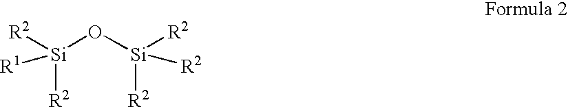
R1 is a cleavable organic functional group, selected from the group consisting of C2 to C6 alkene, C2 to C6 alkyne, C3 to C4 allyl, C1 to C6 alkyl, C1 to C6 perfluoroalkyl; ligand X as described hereinbelow, and ligand Y as described hereinbelow; and
each of R2 is same or different and each of R2 is selected from the group consisting of H, ligand X as described hereinbelow, ligand Y as described hereinbelow, C2 to C6 alkene, C2 to C6 alkyne, C3 to C4 allyl, C1 to C6 alkyl, C1 to C6 perfluoroalkyl, C1 to C6 alkoxy, aryl, perfluoroaryl and C2 to C6 alkylsilane; and
wherein
R1 is a cleavable organic functional group, selected from the group consisting of C2 to C6 alkene, C2 to C6 alkyne, C3 to C4 allyl, C1 to C6 alkyl, C1 to C6 perfluoroalkyl; ligand X as described hereinbelow, and ligand Y as described hereinbelow; and
each of R2 is same or different and each of R2 is selected from the group consisting of H, ligand X as described hereinbelow, ligand Y as described hereinbelow, C2 to C6 alkene, C2 to C6 alkyne, C3 to C4 allyl, C1 to C6 alkyl, C1 to C6 perfluoroalkyl, C1 to C6 alkoxy, aryl, perfluoroaryl and C2 to C6 alkylsilane.
20. The CVD process according to claim 12 , wherein the organosilicon precursor is diformatodimethylsilane.
21. The CVD process according to claim 12 , wherein the organosilicon precursor is selected from the group consisting of: di(formato)methylsilane; di(formato)dimethylsilane; tri(formato) methylsilane; 1,3-dimethyl-1,1,3,3-tetra(formato)disiloxane; 1,3-di(formato)-1,3-disiloxane; diethyldimethylsilane; triethylmethylsilane; 1,1,3,3-diethyl-1,3-dimethyldisiloxane; di-t-butylsilane; 1,3-di-t-butyl-1,1,3,3-tetramethyldisiloxane; di-isopropylsilane; 1,3-di-isopropyl-1,1,3,3-tetramethyldisiloxane; di-isobutylsilane; 1,3-isobutyl-1,1,3,3,-tetramethyldisiloxane; t-butylsilane; 1,3-di-t-butyl-1,1,3,3-tetramethyldisiloxane; 1,3-diethynyl-1,1,3,3-tetramethyldisiloxane; 1,3-diethynyl-1,3-dimethyldisiloxane; 1,3-divinyl-1,1,3,3-tetramethyldisiloxane and 1,3 divinyl-1,3-dimethyldisiloxane.
22. The CVD process according to claim 13 , wherein the organosilicon precursor is selected from the group consisting of:

wherein


ligand X is a cleavable organic functional group as depicted in Formula 3;
R3 is selected from the group consisting of: H, C1 to C6 alkyl, C1 to C6 perfluoroalkyl, C1 to C6 carboxylate, aryl and perfluoroaryl;
R is selected from the group consisting of: C1 to C4 alkyl and C1 to C4 perfluoroalkyl;
and
each of R2 is same or different and each of R2 is selected from the group consisting of H, ligand X as described hereinabove, ligand Y as described hereinbelow, C2 to C6 alkene, C2 to C6 alkyne, C3 to C4 allyl, C1 to C4 alkyl, C1 to C4 perfluoroalkyl, C1 to C6 alkoxy, aryl, perfluoroaryl and C2 to C6 alkylsilane;
wherein
R4 is a cleavable organic functional group selected from the group consisting of: C2 to C6 alkene, and C2 to C6 alkyne, C3 to C4 allyl, C1 to C6 alkyl, C1 to C6 perfluoroalkyl; C1 to C6 alkylsilane, and ligand Y as described hereinbelow;
R is selected from the group consisting of: C1 to C4 alkyl and C1 to C4 perfluoroalkyl; and
each of R2 is same or different and each of R2 is selected from the group consisting of H, ligand X as described hereinabove, ligand Y as described hereinbelow, C2 to C6 alkene, C2 to C6 alkyne, C3 to C4 allyl, C1 to C4 alkyl, C1 to C4 perfluoroalkyl, C1 to C6 alkoxy, aryl, perfluoroaryl and C2 to C6 alkylsilane;
wherein
ligand Y is a cleavable organic functional group as depicted in Formula 3;
R3 is selected from the group consisting of: H, C1 to C6 alkyl, C1 to C6 perfluoroalkyl aryl; perfluoroaryl and C1 to C6 carboxylate;,
R is selected from the group consisting of: C1 to C4 alkyl and C1 to C4 perfluoroalkyl; and
each of R2 is same or different and each of R2 is selected from the group consisting of H, ligand X as described hereinabove, ligand Y as described hereinbelow, C2 to C6 alkene, C2 to C6 alkyne, C3 to C4 allyl, C1 to C4 alkyl, C1 to C4 perfluoroalkyl, C1 to C6 alkoxy, aryl, perfluoroaryl and C2 to C6 alkylsilane;
wherein
R4 is a cleavable organic functional group selected from the group consisting of: C2 to C6 alkene, and C2 to C6 alkyne, C3 to C4 allyl, C1 to C6 alkyl, C1 to C6 perfluoroalkyl; C1 to C6 alkylsilane, and ligand Y as described hereinabove;
each of R is same or different and each of R is selected from the group consisting of: C1 to C4 alkyl and C1 to C4 perfluoroalkyl; and
each of R2 is same or different and each of R2 is selected from the group consisting of H, ligand X as described hereinabove, ligand Y as described hereinabove, C2 to C6 alkene, C2 to C6 alkyne, C3 to C4 allyl, C1 to C4 alkyl, C1 to C4 perfluoroalkyl, C1 to C6 alkoxy, aryl, perfluoroaryl and C2 to C6 alkylsilane; and
wherein
R5 is optional and may be selected from the group consisting of C1 to C2 alkyl;
R is selected from the group consisting of. C1 to C4 alkyl and C1 to C4 perfluoroalkyl; and
R2 is selected from the group consisting of H, ligand X as described hereinabove, ligand Y as described hereinabove, C2 to C6 alkene, C2 to C6 alkyne, C3 to C4 allyl, C1 to C4 alkyl, C1 to C4 perfluoroalkyl, C1 to C6 alkoxy, aryl, perfluoroaryl and C2 to C6 alkylsilane.
23. The CVD process according to claim 13 wherein the organosilicon precursor is diformatodimethylsilane.
24. The CVD process according to claim 13 wherein the organosilicon precursor is selected from the group consisting of: di(formato)methylsilane; di(formato)dimethylsilane; tri(formato)methylsilane; 1,3-dimethyl-1,1,3,3-tetra(formato)disiloxane; 1,3-di(formato)disiloxane; 1,3-diethynyl-1,1,3,3-tetramethyldisiloxane; 1,3-diethynyl-1,3-dimethyldisiloxane; 1,3-divinyl-1,1,3,3-tetramethyldisiloxane and 1,3-divinyl-1,3-dimethyldisiloxane.
25. The CVD process according to claim 10 , wherein the CVD process comprises more than one organosilicon precursor.
26. The CVD process according to claim 12 , wherein the CVD process further comprises a process gas.
27. The CVD process according to claim 26 , wherein the process gas is selected from the group consisting of: CO2, ethylene, acetylene, N2O, O2, H2 and mixtures thereof.
28. The CVD process according to claim 12 , wherein the organosilicon vapor comprises between 1 and 100 percent by volume of an organosilicon precursor vapor and between 1 to about 100 percent by volume of an inert carrier gas, based on the total volume of organosilicon precursor vapor and the inert carrier gas.
29. The CVD process according to claim 12 , wherein the inert carrier gas is selected from the group consisting of argon and helium.
30. The CVD process according to claim 12 , wherein the organosilicon vapor comprises between 1 and 100 percent by volume of an organosilicon precursor vapor, between 1 and 100 percent by volume of an inert carrier gas, and about 1 to 100 percent by volume of a co-reactant, based on the total volume of organosilicon precursor vapor, the inert carrier gas and the co-reactant.
31. The CVD process according to claim 12 , wherein the inert carrier gas is selected from the group consisting of argon and helium.
32. The CVD process according to claim 30 , wherein the co-reactant is selected from the group consisting of: CO2, ethylene, acetylene, N2O, O2, H2 and mixtures thereof.
33. The CVD process according to claim 12 , wherein the organosilicon composition retains between 50 to 95 percent of the original cleavable organic functional groups.
34. The CVD process according to claim 12 , wherein the CVD conditions include a chamber temperature in the chamber in a range of from about 50° C. to about 400° C.
35. The CVD process according to claim 12 , wherein the CVD conditions include a chamber temperature in a range of between 250° C. to about 350° C.
36. The CVD process according to claim 12 , wherein the CVD conditions include a chamber pressure in a range of from about 500 mTorr to about 10 Torr.
37. The CVD process according to claim 12 , wherein the CVD conditions include a chamber pressure of about 4 Torr.
38. The CVD process according to claim 12 , wherein the CVD conditions include a single or mixed frequency RF power source.
39. The CVD process according to claim 12 , wherein the annealing step further comprises an oxidizing or reducing gas.
40. The CVD process according to claim 12 , wherein the-annealing step occurs under plasma-enhanced or oxygen assisted plasma conditions.
41. The CVD process according to claim 12 , wherein the organosilicon thin film is annealed at a gradually increasing temperature profile to a temperature between 100°C. and 400° C.
42. The CVD process according to claim 12 , wherein the organosilicon thin film is annealed at a temperature of 400° C.
43. The CVD process according to claim 12 , wherein the annealing step further comprises CO2.
44. The CVD process according to claim 12 , wherein the annealing step further comprises an oxidizing gas, a reducing gas or combinations thereof.
45. The CVD process according to claim 12 , wherein the annealing step further comprises an oxidizing gas selected from the group consisting of: O2, O3, N2O, NO and combinations thereof.
46. The CVD process according to claim 12 , wherein the annealing step further comprises a reducing gas selected from the group consisting of H2 or NH3.
47. The CVD process according to claim 12 , wherein the annealing step further comprises an inert gas selected from the group consisting of: He, Ar and combinations thereof.
48. The CVD process according to claim 12 , wherein the microporous, low dielectric constant, SiOC thin film comprises between 5 and 99 percent porosity.
49. The CVD process according to claim 12 , wherein the microporous, low dielectric constant SiOC thin film comprises between 5 and 80 percent porosity.
50. The CVD process according to claim 12 , wherein the microporous, low dielectric constant SiOC thin film comprises between 5 and 70 percent porosity.
51. The CVD process according to claim 12 , wherein the microporous, low dielectric constant SiOC thin film comprises between 1 and 20 atomic percent carbon.
52. The CVD process according to claim 12 , wherein the microporous, low dielectric constant SiOC thin film comprises between 1 and 15 atomic percent carbon.
53. The CVD process according to claim 12 , wherein the microporous, low dielectric constant SiOC thin film comprises between 1 and 10 percent carbon.
54. The CVD process according to claim 12 , wherein the microporous, low dielectric constant SiOC thin film comprises a dielectric constant of less than 3.0.
55. The CVD process according to claim 12 , wherein the microporous, low dielectric constant SiOC thin film comprises a dielectric constant of less than 2.0.
56. The CVD process according to claim 12 , wherein the microporous, low dielectric constant SiOC thin film comprises a dielectric constant of less than 1.5.
57. A porous, low dielectric constant thin film made by the process of claim 12.
Priority Applications (2)
| Application Number | Priority Date | Filing Date | Title |
|---|---|---|---|
| US09/811,106 US20020172766A1 (en) | 2001-03-17 | 2001-03-17 | Low dielectric constant thin films and chemical vapor deposition method of making same |
| US10/937,434 US20050038276A1 (en) | 2001-03-17 | 2004-09-09 | Low dielectric constant thin films and chemical vapor deposition method of making same |
Applications Claiming Priority (1)
| Application Number | Priority Date | Filing Date | Title |
|---|---|---|---|
| US09/811,106 US20020172766A1 (en) | 2001-03-17 | 2001-03-17 | Low dielectric constant thin films and chemical vapor deposition method of making same |
Related Child Applications (1)
| Application Number | Title | Priority Date | Filing Date |
|---|---|---|---|
| US10/937,434 Continuation US20050038276A1 (en) | 2001-03-17 | 2004-09-09 | Low dielectric constant thin films and chemical vapor deposition method of making same |
Publications (1)
| Publication Number | Publication Date |
|---|---|
| US20020172766A1 true US20020172766A1 (en) | 2002-11-21 |
Family
ID=25205576
Family Applications (2)
| Application Number | Title | Priority Date | Filing Date |
|---|---|---|---|
| US09/811,106 Abandoned US20020172766A1 (en) | 2001-03-17 | 2001-03-17 | Low dielectric constant thin films and chemical vapor deposition method of making same |
| US10/937,434 Abandoned US20050038276A1 (en) | 2001-03-17 | 2004-09-09 | Low dielectric constant thin films and chemical vapor deposition method of making same |
Family Applications After (1)
| Application Number | Title | Priority Date | Filing Date |
|---|---|---|---|
| US10/937,434 Abandoned US20050038276A1 (en) | 2001-03-17 | 2004-09-09 | Low dielectric constant thin films and chemical vapor deposition method of making same |
Country Status (1)
| Country | Link |
|---|---|
| US (2) | US20020172766A1 (en) |
Cited By (52)
| Publication number | Priority date | Publication date | Assignee | Title |
|---|---|---|---|---|
| US20030064154A1 (en) * | 2001-08-06 | 2003-04-03 | Laxman Ravi K. | Low-K dielectric thin films and chemical vapor deposition method of making same |
| US20030139035A1 (en) * | 2001-12-14 | 2003-07-24 | Applied Materials, Inc. | Low dielectric (low k) barrier films with oxygen doping by plasma-enhanced chemical vapor deposition (pecvd) |
| US20030211728A1 (en) * | 2000-01-18 | 2003-11-13 | Applied Materials, Inc. | Very low dielectric constant plasma-enhanced CVD films |
| US20040009676A1 (en) * | 2002-07-11 | 2004-01-15 | Applied Materials, Inc. | Nitrogen-free dielectric anti-reflective coating and hardmask |
| US20040061201A1 (en) * | 2001-12-14 | 2004-04-01 | Ebrahim Andideh | Low-dielectric constant structure with a multilayer stack of thin films with pores |
| FR2848036A1 (en) * | 2002-11-28 | 2004-06-04 | St Microelectronics Sa | SUPPORT FOR ACOUSTIC RESONATOR, ACOUSTIC RESONATOR AND CORRESPONDING INTEGRATED CIRCUIT |
| US20040227242A1 (en) * | 2003-03-25 | 2004-11-18 | Renesas Technology Corp. | Semiconductor device and manufacturing method thereof |
| US20040241463A1 (en) * | 2003-05-29 | 2004-12-02 | Vincent Jean Louise | Mechanical enhancer additives for low dielectric films |
| US20040253378A1 (en) * | 2003-06-12 | 2004-12-16 | Applied Materials, Inc. | Stress reduction of SIOC low k film by addition of alkylenes to OMCTS based processes |
| US20050038276A1 (en) * | 2001-03-17 | 2005-02-17 | Laxman Ravi K. | Low dielectric constant thin films and chemical vapor deposition method of making same |
| US20050059264A1 (en) * | 1998-09-29 | 2005-03-17 | David Cheung | CVD plasma assisted low dielectric constant films |
| US20050130404A1 (en) * | 2002-05-08 | 2005-06-16 | Applied Materials, Inc. | Methods and apparatus for e-beam treatment used to fabricate integrated circuit devices |
| US7125813B2 (en) | 2001-10-09 | 2006-10-24 | Applied Materials, Inc. | Method of depositing low K barrier layers |
| US20070026321A1 (en) * | 2005-07-29 | 2007-02-01 | Applied Materials, Inc. | Cluster tool and method for process integration in manufacturing of a photomask |
| US20070077778A1 (en) * | 2005-10-04 | 2007-04-05 | The Boc Group, Inc. | Method of forming low dielectric constant layer |
| US20070119373A1 (en) * | 2005-07-29 | 2007-05-31 | Ajay Kumar | Chemical vapor deposition chamber with dual frequency bias and method for manufacturing a photomask using the same |
| US20070152777A1 (en) * | 2005-09-05 | 2007-07-05 | Stmicroelectronics S.A. | Support for acoustic resonator and corresponding integrated circuit |
| US7390537B1 (en) | 2003-11-20 | 2008-06-24 | Novellus Systems, Inc. | Methods for producing low-k CDO films with low residual stress |
| US7473653B1 (en) | 2003-03-31 | 2009-01-06 | Novellus Systems, Inc. | Methods for producing low stress porous low-k dielectric materials using precursors with organic functional groups |
| US7510982B1 (en) | 2005-01-31 | 2009-03-31 | Novellus Systems, Inc. | Creation of porosity in low-k films by photo-disassociation of imbedded nanoparticles |
| US7622162B1 (en) | 2007-06-07 | 2009-11-24 | Novellus Systems, Inc. | UV treatment of STI films for increasing tensile stress |
| US7629224B1 (en) | 2005-01-31 | 2009-12-08 | Novellus Systems, Inc. | VLSI fabrication processes for introducing pores into dielectric materials |
| US7695765B1 (en) | 2004-11-12 | 2010-04-13 | Novellus Systems, Inc. | Methods for producing low-stress carbon-doped oxide films with improved integration properties |
| US7737525B1 (en) | 2004-03-11 | 2010-06-15 | Novellus Systems, Inc. | Method for producing low-K CDO films |
| US7749563B2 (en) | 2002-10-07 | 2010-07-06 | Applied Materials, Inc. | Two-layer film for next generation damascene barrier application with good oxidation resistance |
| US20100210107A1 (en) * | 2002-10-17 | 2010-08-19 | Renesas Technology Corp. | Semiconductor device and manufacturing method thereof |
| US7781351B1 (en) | 2004-04-07 | 2010-08-24 | Novellus Systems, Inc. | Methods for producing low-k carbon doped oxide films with low residual stress |
| US7790633B1 (en) | 2004-10-26 | 2010-09-07 | Novellus Systems, Inc. | Sequential deposition/anneal film densification method |
| US20100261349A1 (en) * | 2006-10-30 | 2010-10-14 | Novellus Systems, Inc. | Uv treatment for carbon-containing low-k dielectric repair in semiconductor processing |
| US7892985B1 (en) | 2005-11-15 | 2011-02-22 | Novellus Systems, Inc. | Method for porogen removal and mechanical strength enhancement of low-k carbon doped silicon oxide using low thermal budget microwave curing |
| US7906174B1 (en) | 2006-12-07 | 2011-03-15 | Novellus Systems, Inc. | PECVD methods for producing ultra low-k dielectric films using UV treatment |
| US20110117678A1 (en) * | 2006-10-30 | 2011-05-19 | Varadarajan Bhadri N | Carbon containing low-k dielectric constant recovery using uv treatment |
| US20110204492A1 (en) * | 2010-02-23 | 2011-08-25 | Applied Materials, Inc. | Microelectronic structure including a low K dielectric and a method of controlling carbon distribution in the structure |
| US8043667B1 (en) | 2004-04-16 | 2011-10-25 | Novellus Systems, Inc. | Method to improve mechanical strength of low-K dielectric film using modulated UV exposure |
| US8137465B1 (en) | 2005-04-26 | 2012-03-20 | Novellus Systems, Inc. | Single-chamber sequential curing of semiconductor wafers |
| US8211510B1 (en) | 2007-08-31 | 2012-07-03 | Novellus Systems, Inc. | Cascaded cure approach to fabricate highly tensile silicon nitride films |
| US8242028B1 (en) | 2007-04-03 | 2012-08-14 | Novellus Systems, Inc. | UV treatment of etch stop and hard mask films for selectivity and hermeticity enhancement |
| US8282768B1 (en) | 2005-04-26 | 2012-10-09 | Novellus Systems, Inc. | Purging of porogen from UV cure chamber |
| US8454750B1 (en) | 2005-04-26 | 2013-06-04 | Novellus Systems, Inc. | Multi-station sequential curing of dielectric films |
| US8889233B1 (en) | 2005-04-26 | 2014-11-18 | Novellus Systems, Inc. | Method for reducing stress in porous dielectric films |
| US8980769B1 (en) | 2005-04-26 | 2015-03-17 | Novellus Systems, Inc. | Multi-station sequential curing of dielectric films |
| US9050623B1 (en) | 2008-09-12 | 2015-06-09 | Novellus Systems, Inc. | Progressive UV cure |
| US20160118621A1 (en) * | 2013-06-21 | 2016-04-28 | Universal Display Corporation | Hybrid barrier layer for substrates and electronic devices |
| US9659769B1 (en) | 2004-10-22 | 2017-05-23 | Novellus Systems, Inc. | Tensile dielectric films using UV curing |
| US9847221B1 (en) | 2016-09-29 | 2017-12-19 | Lam Research Corporation | Low temperature formation of high quality silicon oxide films in semiconductor device manufacturing |
| US20180122858A1 (en) * | 2016-05-20 | 2018-05-03 | Micron Technology, Inc. | Array Of Memory Cells |
| US10037905B2 (en) | 2009-11-12 | 2018-07-31 | Novellus Systems, Inc. | UV and reducing treatment for K recovery and surface clean in semiconductor processing |
| US10461128B2 (en) | 2017-04-26 | 2019-10-29 | Micron Technology, Inc. | Arrays of memory cells and methods of forming an array of elevationally-outer-tier memory cells and elevationally-inner-tier memory cells |
| CN111599925A (en) * | 2020-05-29 | 2020-08-28 | 河南大学 | Solar cell with dimethyl tin bis (formate) N-type semiconductor film as electron transport layer and preparation method thereof |
| US20210111025A1 (en) * | 2019-10-10 | 2021-04-15 | Asm Ip Holding B.V. | Method of forming a photoresist underlayer and structure including same |
| CN116497340A (en) * | 2023-06-21 | 2023-07-28 | 上海陛通半导体能源科技股份有限公司 | Method for forming low-temperature silicon oxycarbide film |
| US11751426B2 (en) | 2016-10-18 | 2023-09-05 | Universal Display Corporation | Hybrid thin film permeation barrier and method of making the same |
Families Citing this family (5)
| Publication number | Priority date | Publication date | Assignee | Title |
|---|---|---|---|---|
| US6486082B1 (en) * | 2001-06-18 | 2002-11-26 | Applied Materials, Inc. | CVD plasma assisted lower dielectric constant sicoh film |
| KR100864001B1 (en) * | 2002-06-14 | 2008-10-16 | 삼성전자주식회사 | Organic electroluminescent device |
| US6737365B1 (en) * | 2003-03-24 | 2004-05-18 | Intel Corporation | Forming a porous dielectric layer |
| US20060289966A1 (en) * | 2005-06-22 | 2006-12-28 | Dani Ashay A | Silicon wafer with non-soluble protective coating |
| US20070287849A1 (en) | 2006-06-13 | 2007-12-13 | Air Products And Chemicals, Inc. | Low-Impurity Organosilicon Product As Precursor For CVD |
Citations (1)
| Publication number | Priority date | Publication date | Assignee | Title |
|---|---|---|---|---|
| US3313648A (en) * | 1965-04-05 | 1967-04-11 | Boeing Co | Treatment of glass glazing vulnerable to impact by insects |
Family Cites Families (18)
| Publication number | Priority date | Publication date | Assignee | Title |
|---|---|---|---|---|
| US3197433A (en) * | 1962-07-02 | 1965-07-27 | Gen Electric | Optically clear organopolysiloxane resins |
| US3296195A (en) * | 1963-12-20 | 1967-01-03 | Gen Electric | Curable composition |
| US3676418A (en) * | 1968-07-20 | 1972-07-11 | Mitsubishi Petrochemical Co | Catalytic production of olefin polymers |
| US3884891A (en) * | 1972-07-17 | 1975-05-20 | Sergei Mikhailovich Samoilov | Method for preparing branched copolymers by ethylene with unsaturated silicone monomers |
| US4044038A (en) * | 1973-10-24 | 1977-08-23 | Th. Goldschmidt Ag | Process for the manufacture of at least substantially balanced organopolysiloxane mixtures with silyl halide groupings |
| US5204134A (en) * | 1989-01-13 | 1993-04-20 | Immuno Path Profile, Inc. | Hypoallergenic milk products from natural and/or synthetic components and process of making |
| US5362328A (en) * | 1990-07-06 | 1994-11-08 | Advanced Technology Materials, Inc. | Apparatus and method for delivering reagents in vapor form to a CVD reactor, incorporating a cleaning subsystem |
| US5711816A (en) * | 1990-07-06 | 1998-01-27 | Advanced Technolgy Materials, Inc. | Source reagent liquid delivery apparatus, and chemical vapor deposition system comprising same |
| US5478920A (en) * | 1993-07-16 | 1995-12-26 | E. I. Du Pont De Nemours And Company | Cyclic ether polymerization using silicon compound accelerators |
| US5948928A (en) * | 1996-12-05 | 1999-09-07 | Advanced Delivery & Chemical Systems, Ltd. | Mono, di- and trifluoroacetate substituted silanes |
| US6048804A (en) * | 1997-04-29 | 2000-04-11 | Alliedsignal Inc. | Process for producing nanoporous silica thin films |
| US6383955B1 (en) * | 1998-02-05 | 2002-05-07 | Asm Japan K.K. | Silicone polymer insulation film on semiconductor substrate and method for forming the film |
| US6054206A (en) * | 1998-06-22 | 2000-04-25 | Novellus Systems, Inc. | Chemical vapor deposition of low density silicon dioxide films |
| US6022812A (en) * | 1998-07-07 | 2000-02-08 | Alliedsignal Inc. | Vapor deposition routes to nanoporous silica |
| US6171945B1 (en) * | 1998-10-22 | 2001-01-09 | Applied Materials, Inc. | CVD nanoporous silica low dielectric constant films |
| US6340628B1 (en) * | 2000-12-12 | 2002-01-22 | Novellus Systems, Inc. | Method to deposit SiOCH films with dielectric constant below 3.0 |
| US20020172766A1 (en) * | 2001-03-17 | 2002-11-21 | Laxman Ravi K. | Low dielectric constant thin films and chemical vapor deposition method of making same |
| US20030064154A1 (en) * | 2001-08-06 | 2003-04-03 | Laxman Ravi K. | Low-K dielectric thin films and chemical vapor deposition method of making same |
-
2001
- 2001-03-17 US US09/811,106 patent/US20020172766A1/en not_active Abandoned
-
2004
- 2004-09-09 US US10/937,434 patent/US20050038276A1/en not_active Abandoned
Patent Citations (1)
| Publication number | Priority date | Publication date | Assignee | Title |
|---|---|---|---|---|
| US3313648A (en) * | 1965-04-05 | 1967-04-11 | Boeing Co | Treatment of glass glazing vulnerable to impact by insects |
Cited By (112)
| Publication number | Priority date | Publication date | Assignee | Title |
|---|---|---|---|---|
| US7205249B2 (en) | 1998-09-29 | 2007-04-17 | Applied Materials, Inc. | CVD plasma assisted low dielectric constant films |
| US20050059264A1 (en) * | 1998-09-29 | 2005-03-17 | David Cheung | CVD plasma assisted low dielectric constant films |
| US20050136240A1 (en) * | 2000-01-18 | 2005-06-23 | Mandal Robert P. | Very low dielectric constant plasma-enhanced CVD films |
| US20030211728A1 (en) * | 2000-01-18 | 2003-11-13 | Applied Materials, Inc. | Very low dielectric constant plasma-enhanced CVD films |
| US7094710B2 (en) | 2000-01-18 | 2006-08-22 | Applied Materials | Very low dielectric constant plasma-enhanced CVD films |
| US7825042B2 (en) | 2000-01-18 | 2010-11-02 | Applied Materials, Inc. | Very low dielectric constant plasma-enhanced CVD films |
| US7633163B2 (en) | 2000-01-18 | 2009-12-15 | Applied Materials, Inc. | Very low dielectric constant plasma-enhanced CVD films |
| US7601631B2 (en) | 2000-01-18 | 2009-10-13 | Appplied Materials, Inc. | Very low dielectric constant plasma-enhanced CVD films |
| US7399697B2 (en) | 2000-01-18 | 2008-07-15 | Applied Materials, Inc. | Very low dielectric constant plasma-enhanced CVD films |
| US20060226548A1 (en) * | 2000-01-18 | 2006-10-12 | Mandal Robert P | Very low dielectric constant plasma-enhanced cvd films |
| US7205224B2 (en) | 2000-01-18 | 2007-04-17 | Applied Materials, Inc. | Very low dielectric constant plasma-enhanced CVD films |
| US20050038276A1 (en) * | 2001-03-17 | 2005-02-17 | Laxman Ravi K. | Low dielectric constant thin films and chemical vapor deposition method of making same |
| US20030064154A1 (en) * | 2001-08-06 | 2003-04-03 | Laxman Ravi K. | Low-K dielectric thin films and chemical vapor deposition method of making same |
| US7319068B2 (en) | 2001-10-09 | 2008-01-15 | Applied Materials, Inc. | Method of depositing low k barrier layers |
| US20070042610A1 (en) * | 2001-10-09 | 2007-02-22 | Li-Qun Xia | Method of depositing low k barrier layers |
| US7125813B2 (en) | 2001-10-09 | 2006-10-24 | Applied Materials, Inc. | Method of depositing low K barrier layers |
| US20030139035A1 (en) * | 2001-12-14 | 2003-07-24 | Applied Materials, Inc. | Low dielectric (low k) barrier films with oxygen doping by plasma-enhanced chemical vapor deposition (pecvd) |
| US6838393B2 (en) | 2001-12-14 | 2005-01-04 | Applied Materials, Inc. | Method for producing semiconductor including forming a layer containing at least silicon carbide and forming a second layer containing at least silicon oxygen carbide |
| US7034380B2 (en) * | 2001-12-14 | 2006-04-25 | Intel Corporation | Low-dielectric constant structure with a multilayer stack of thin films with pores |
| US20040061201A1 (en) * | 2001-12-14 | 2004-04-01 | Ebrahim Andideh | Low-dielectric constant structure with a multilayer stack of thin films with pores |
| US7256139B2 (en) | 2002-05-08 | 2007-08-14 | Applied Materials, Inc. | Methods and apparatus for e-beam treatment used to fabricate integrated circuit devices |
| US20050130404A1 (en) * | 2002-05-08 | 2005-06-16 | Applied Materials, Inc. | Methods and apparatus for e-beam treatment used to fabricate integrated circuit devices |
| US20040009676A1 (en) * | 2002-07-11 | 2004-01-15 | Applied Materials, Inc. | Nitrogen-free dielectric anti-reflective coating and hardmask |
| US7749563B2 (en) | 2002-10-07 | 2010-07-06 | Applied Materials, Inc. | Two-layer film for next generation damascene barrier application with good oxidation resistance |
| US20100210107A1 (en) * | 2002-10-17 | 2010-08-19 | Renesas Technology Corp. | Semiconductor device and manufacturing method thereof |
| US8012871B2 (en) | 2002-10-17 | 2011-09-06 | Renesas Electronics Corporation | Semiconductor device and manufacturing method thereof |
| WO2004051848A1 (en) * | 2002-11-28 | 2004-06-17 | Stmicroelectronics Sa | Acoustic resonator support, acoustic resonator and corresponding integrated circuit |
| US7391142B2 (en) * | 2002-11-28 | 2008-06-24 | Stmicroelectronics S.A. | Acoustic resonator support, acoustic resonator and corresponding integrated circuit |
| US20060226736A1 (en) * | 2002-11-28 | 2006-10-12 | Guillaume Bouche | Acoustic resonator support, acoustic resonator and corresponding integrated circuit |
| US20050023931A1 (en) * | 2002-11-28 | 2005-02-03 | Stmicroelectronics S.A. | Support and decoupling structure for an acoustic resonator, acoustic resonator and corresponding integrated circuit |
| US20070182284A1 (en) * | 2002-11-28 | 2007-08-09 | Guillaume Bouche | Support and decoupling structure for an acoustic resonator, acoustic resonator and corresponding integrated circuit |
| US7391143B2 (en) | 2002-11-28 | 2008-06-24 | Stmicroelectronics S.A. | Support and decoupling structure for an acoustic resonator, acoustic resonator and corresponding integrated circuit |
| FR2848036A1 (en) * | 2002-11-28 | 2004-06-04 | St Microelectronics Sa | SUPPORT FOR ACOUSTIC RESONATOR, ACOUSTIC RESONATOR AND CORRESPONDING INTEGRATED CIRCUIT |
| US20060226555A1 (en) * | 2003-03-25 | 2006-10-12 | Junji Noguchi | Semiconductor device and manufacturing method thereof |
| US7777343B2 (en) | 2003-03-25 | 2010-08-17 | Renesas Technology Corp. | Semiconductor device and manufacturing method thereof |
| US7323781B2 (en) | 2003-03-25 | 2008-01-29 | Renesas Technology Corp. | Semiconductor device and manufacturing method thereof |
| US8810034B2 (en) | 2003-03-25 | 2014-08-19 | Renesas Electronics Corporation | Semiconductor device and manufacturing method thereof |
| US9818639B2 (en) | 2003-03-25 | 2017-11-14 | Renesas Electronics Corporation | Semiconductor device and manufacturing method thereof |
| US10304726B2 (en) | 2003-03-25 | 2019-05-28 | Renesas Electronics Corporation | Semiconductor device and manufacturing method thereof |
| US9659867B2 (en) | 2003-03-25 | 2017-05-23 | Renesas Electronics Corporation | Semiconductor device and manufacturing method thereof |
| CN100373609C (en) * | 2003-03-25 | 2008-03-05 | 株式会社瑞萨科技 | Semiconductor device and its mfg. method |
| US20040227242A1 (en) * | 2003-03-25 | 2004-11-18 | Renesas Technology Corp. | Semiconductor device and manufacturing method thereof |
| US20090256261A1 (en) * | 2003-03-25 | 2009-10-15 | Renesas Technology Corp. | Semiconductor device and manufacturing method thereof |
| US9490213B2 (en) | 2003-03-25 | 2016-11-08 | Renesas Electronics Corporation | Semiconductor device and manufacturing method thereof |
| US8431480B2 (en) | 2003-03-25 | 2013-04-30 | Renesas Electronics Corporation | Semiconductor device and manufacturing method thereof |
| US10121693B2 (en) | 2003-03-25 | 2018-11-06 | Renesas Electronics Corporation | Semiconductor device and manufacturing method thereof |
| US9064870B2 (en) | 2003-03-25 | 2015-06-23 | Renesas Electronics Corporation | Semiconductor device and manufacturing method thereof |
| US8617981B2 (en) | 2003-03-25 | 2013-12-31 | Renesas Electronics Corporation | Semiconductor device and manufacturing method thereof |
| US8053893B2 (en) | 2003-03-25 | 2011-11-08 | Renesas Electronics Corporation | Semiconductor device and manufacturing method thereof |
| US7473653B1 (en) | 2003-03-31 | 2009-01-06 | Novellus Systems, Inc. | Methods for producing low stress porous low-k dielectric materials using precursors with organic functional groups |
| US7799705B1 (en) | 2003-03-31 | 2010-09-21 | Novellus Systems, Inc. | Methods for producing low stress porous low-k dielectric materials using precursors with organic functional groups |
| US7923385B2 (en) | 2003-03-31 | 2011-04-12 | Novellus Systems, Inc. | Methods for producing low stress porous and CDO low-K dielectric materials using precursors with organic functional groups |
| US8137764B2 (en) | 2003-05-29 | 2012-03-20 | Air Products And Chemicals, Inc. | Mechanical enhancer additives for low dielectric films |
| US20040241463A1 (en) * | 2003-05-29 | 2004-12-02 | Vincent Jean Louise | Mechanical enhancer additives for low dielectric films |
| US20040253378A1 (en) * | 2003-06-12 | 2004-12-16 | Applied Materials, Inc. | Stress reduction of SIOC low k film by addition of alkylenes to OMCTS based processes |
| US7390537B1 (en) | 2003-11-20 | 2008-06-24 | Novellus Systems, Inc. | Methods for producing low-k CDO films with low residual stress |
| US7737525B1 (en) | 2004-03-11 | 2010-06-15 | Novellus Systems, Inc. | Method for producing low-K CDO films |
| US7781351B1 (en) | 2004-04-07 | 2010-08-24 | Novellus Systems, Inc. | Methods for producing low-k carbon doped oxide films with low residual stress |
| US8715788B1 (en) | 2004-04-16 | 2014-05-06 | Novellus Systems, Inc. | Method to improve mechanical strength of low-K dielectric film using modulated UV exposure |
| US8043667B1 (en) | 2004-04-16 | 2011-10-25 | Novellus Systems, Inc. | Method to improve mechanical strength of low-K dielectric film using modulated UV exposure |
| US9659769B1 (en) | 2004-10-22 | 2017-05-23 | Novellus Systems, Inc. | Tensile dielectric films using UV curing |
| US7790633B1 (en) | 2004-10-26 | 2010-09-07 | Novellus Systems, Inc. | Sequential deposition/anneal film densification method |
| US7695765B1 (en) | 2004-11-12 | 2010-04-13 | Novellus Systems, Inc. | Methods for producing low-stress carbon-doped oxide films with improved integration properties |
| US7629224B1 (en) | 2005-01-31 | 2009-12-08 | Novellus Systems, Inc. | VLSI fabrication processes for introducing pores into dielectric materials |
| US7510982B1 (en) | 2005-01-31 | 2009-03-31 | Novellus Systems, Inc. | Creation of porosity in low-k films by photo-disassociation of imbedded nanoparticles |
| US8062983B1 (en) | 2005-01-31 | 2011-11-22 | Novellus Systems, Inc. | Creation of porosity in low-k films by photo-disassociation of imbedded nanoparticles |
| US7972976B1 (en) | 2005-01-31 | 2011-07-05 | Novellus Systems, Inc. | VLSI fabrication processes for introducing pores into dielectric materials |
| US8629068B1 (en) | 2005-04-26 | 2014-01-14 | Novellus Systems, Inc. | Multi-station sequential curing of dielectric films |
| US8454750B1 (en) | 2005-04-26 | 2013-06-04 | Novellus Systems, Inc. | Multi-station sequential curing of dielectric films |
| US10121682B2 (en) | 2005-04-26 | 2018-11-06 | Novellus Systems, Inc. | Purging of porogen from UV cure chamber |
| US9873946B2 (en) | 2005-04-26 | 2018-01-23 | Novellus Systems, Inc. | Multi-station sequential curing of dielectric films |
| US8137465B1 (en) | 2005-04-26 | 2012-03-20 | Novellus Systems, Inc. | Single-chamber sequential curing of semiconductor wafers |
| US9384959B2 (en) | 2005-04-26 | 2016-07-05 | Novellus Systems, Inc. | Purging of porogen from UV cure chamber |
| US8980769B1 (en) | 2005-04-26 | 2015-03-17 | Novellus Systems, Inc. | Multi-station sequential curing of dielectric films |
| US8889233B1 (en) | 2005-04-26 | 2014-11-18 | Novellus Systems, Inc. | Method for reducing stress in porous dielectric films |
| US8282768B1 (en) | 2005-04-26 | 2012-10-09 | Novellus Systems, Inc. | Purging of porogen from UV cure chamber |
| US8734663B2 (en) | 2005-04-26 | 2014-05-27 | Novellus Systems, Inc. | Purging of porogen from UV cure chamber |
| US8518210B2 (en) | 2005-04-26 | 2013-08-27 | Novellus Systems, Inc. | Purging of porogen from UV cure chamber |
| US20070023390A1 (en) * | 2005-07-29 | 2007-02-01 | Ajay Kumar | Cluster tool and method for process integration in manufacturing of a photomask |
| US20070026321A1 (en) * | 2005-07-29 | 2007-02-01 | Applied Materials, Inc. | Cluster tool and method for process integration in manufacturing of a photomask |
| US20070119373A1 (en) * | 2005-07-29 | 2007-05-31 | Ajay Kumar | Chemical vapor deposition chamber with dual frequency bias and method for manufacturing a photomask using the same |
| US7658969B2 (en) * | 2005-07-29 | 2010-02-09 | Applied Materials, Inc. | Chemical vapor deposition chamber with dual frequency bias and method for manufacturing a photomask using the same |
| US7838433B2 (en) | 2005-07-29 | 2010-11-23 | Applied Materials, Inc. | Cluster tool and method for process integration in manufacturing of a photomask |
| US7829471B2 (en) | 2005-07-29 | 2010-11-09 | Applied Materials, Inc. | Cluster tool and method for process integration in manufacturing of a photomask |
| US20070152777A1 (en) * | 2005-09-05 | 2007-07-05 | Stmicroelectronics S.A. | Support for acoustic resonator and corresponding integrated circuit |
| US7737804B2 (en) * | 2005-09-05 | 2010-06-15 | Stmicroelectronics S.A. | Support for acoustic resonator and corresponding integrated circuit |
| US20070077778A1 (en) * | 2005-10-04 | 2007-04-05 | The Boc Group, Inc. | Method of forming low dielectric constant layer |
| US7892985B1 (en) | 2005-11-15 | 2011-02-22 | Novellus Systems, Inc. | Method for porogen removal and mechanical strength enhancement of low-k carbon doped silicon oxide using low thermal budget microwave curing |
| US8465991B2 (en) | 2006-10-30 | 2013-06-18 | Novellus Systems, Inc. | Carbon containing low-k dielectric constant recovery using UV treatment |
| US7851232B2 (en) | 2006-10-30 | 2010-12-14 | Novellus Systems, Inc. | UV treatment for carbon-containing low-k dielectric repair in semiconductor processing |
| US20100261349A1 (en) * | 2006-10-30 | 2010-10-14 | Novellus Systems, Inc. | Uv treatment for carbon-containing low-k dielectric repair in semiconductor processing |
| US20110117678A1 (en) * | 2006-10-30 | 2011-05-19 | Varadarajan Bhadri N | Carbon containing low-k dielectric constant recovery using uv treatment |
| US7906174B1 (en) | 2006-12-07 | 2011-03-15 | Novellus Systems, Inc. | PECVD methods for producing ultra low-k dielectric films using UV treatment |
| US8242028B1 (en) | 2007-04-03 | 2012-08-14 | Novellus Systems, Inc. | UV treatment of etch stop and hard mask films for selectivity and hermeticity enhancement |
| US7622162B1 (en) | 2007-06-07 | 2009-11-24 | Novellus Systems, Inc. | UV treatment of STI films for increasing tensile stress |
| US8512818B1 (en) | 2007-08-31 | 2013-08-20 | Novellus Systems, Inc. | Cascaded cure approach to fabricate highly tensile silicon nitride films |
| US8211510B1 (en) | 2007-08-31 | 2012-07-03 | Novellus Systems, Inc. | Cascaded cure approach to fabricate highly tensile silicon nitride films |
| US9050623B1 (en) | 2008-09-12 | 2015-06-09 | Novellus Systems, Inc. | Progressive UV cure |
| US10037905B2 (en) | 2009-11-12 | 2018-07-31 | Novellus Systems, Inc. | UV and reducing treatment for K recovery and surface clean in semiconductor processing |
| US20110204492A1 (en) * | 2010-02-23 | 2011-08-25 | Applied Materials, Inc. | Microelectronic structure including a low K dielectric and a method of controlling carbon distribution in the structure |
| US8349746B2 (en) | 2010-02-23 | 2013-01-08 | Applied Materials, Inc. | Microelectronic structure including a low k dielectric and a method of controlling carbon distribution in the structure |
| US20160118621A1 (en) * | 2013-06-21 | 2016-04-28 | Universal Display Corporation | Hybrid barrier layer for substrates and electronic devices |
| US20180122858A1 (en) * | 2016-05-20 | 2018-05-03 | Micron Technology, Inc. | Array Of Memory Cells |
| US11424291B2 (en) * | 2016-05-20 | 2022-08-23 | Micron Technology, Inc. | Array of cross point memory cells |
| US9847221B1 (en) | 2016-09-29 | 2017-12-19 | Lam Research Corporation | Low temperature formation of high quality silicon oxide films in semiconductor device manufacturing |
| US11751426B2 (en) | 2016-10-18 | 2023-09-05 | Universal Display Corporation | Hybrid thin film permeation barrier and method of making the same |
| US10461128B2 (en) | 2017-04-26 | 2019-10-29 | Micron Technology, Inc. | Arrays of memory cells and methods of forming an array of elevationally-outer-tier memory cells and elevationally-inner-tier memory cells |
| US11302748B2 (en) | 2017-04-26 | 2022-04-12 | Micron Technology, Inc. | Arrays of memory cells and methods of forming an array of elevationally-outer-tier memory cells and elevationally-inner-tier memory cells |
| US20210111025A1 (en) * | 2019-10-10 | 2021-04-15 | Asm Ip Holding B.V. | Method of forming a photoresist underlayer and structure including same |
| US11735422B2 (en) * | 2019-10-10 | 2023-08-22 | Asm Ip Holding B.V. | Method of forming a photoresist underlayer and structure including same |
| CN111599925A (en) * | 2020-05-29 | 2020-08-28 | 河南大学 | Solar cell with dimethyl tin bis (formate) N-type semiconductor film as electron transport layer and preparation method thereof |
| CN116497340A (en) * | 2023-06-21 | 2023-07-28 | 上海陛通半导体能源科技股份有限公司 | Method for forming low-temperature silicon oxycarbide film |
Also Published As
| Publication number | Publication date |
|---|---|
| US20050038276A1 (en) | 2005-02-17 |
Similar Documents
| Publication | Publication Date | Title |
|---|---|---|
| US20020172766A1 (en) | Low dielectric constant thin films and chemical vapor deposition method of making same | |
| US20030064154A1 (en) | Low-K dielectric thin films and chemical vapor deposition method of making same | |
| US7108771B2 (en) | Method for removal of impurities in cyclic siloxanes useful as precursors for low dielectric constant thin films | |
| US5492736A (en) | Fluorine doped silicon oxide process | |
| JP4897505B2 (en) | Chemical vapor deposition method for obtaining low dielectric constant porous organosilica glass films | |
| US7423166B2 (en) | Stabilized cyclosiloxanes for use as CVD precursors for low-dielectric constant thin films | |
| US8293001B2 (en) | Porogens, porogenated precursors and methods for using the same to provide porous organosilica glass films with low dielectric constants | |
| KR100437068B1 (en) | Method of forming a carbon silicon oxide | |
| KR100602469B1 (en) | Mechanical enhancer additives for low dielectric films | |
| US7087271B2 (en) | Method for preparing low dielectric films | |
| US20030194496A1 (en) | Methods for depositing dielectric material | |
| JP5711176B2 (en) | Composition | |
| JP2002256434A (en) | Method of forming low dielectric constant interlayer dielectric film | |
| US20020072220A1 (en) | Low-k dielectric CVD precursors and uses thereof | |
| CN103238206A (en) | In-situ low-k capping to improve integration damage resistance | |
| WO2002043119A3 (en) | An ultralow dielectric constant material as an intralevel or interlevel dielectric in a semiconductor device, a method for fabricating the same, and an electronic device containing the same | |
| JP2003007699A (en) | Low-permittivity material and processing method according to cvd | |
| JPH09172012A (en) | Growth method for coatings containing silicon and oxygen | |
| US6572925B2 (en) | Process for forming a low dielectric constant fluorine and carbon containing silicon oxide dielectric material | |
| US20210339280A1 (en) | Silacyclic compounds and methods for depositing silicon-containing films using same | |
| KR102442026B1 (en) | Alkoxysilacyclic or acyloxysilacyclic compounds and methods for depositing films using same | |
| JP2723472B2 (en) | Apparatus and method for depositing borophosphosilicate glass on a substrate | |
| US7763327B2 (en) | Methods using ozone for CVD deposited films |
Legal Events
| Date | Code | Title | Description |
|---|---|---|---|
| AS | Assignment |
Owner name: ADVANCED TECHNOLOGY MATERIALS, INC., CONNECTICUT Free format text: ASSIGNMENT OF ASSIGNORS INTEREST;ASSIGNORS:LAXMAN, RAVI K.;XU, CHONGYING;BAUM, THOMAS H.;REEL/FRAME:011884/0927;SIGNING DATES FROM 20010309 TO 20010405 |
|
| STCB | Information on status: application discontinuation |
Free format text: ABANDONED -- FAILURE TO RESPOND TO AN OFFICE ACTION |