EP3096370A1 - Chiplet display with multiple passive-matrix controllers - Google Patents
Chiplet display with multiple passive-matrix controllers Download PDFInfo
- Publication number
- EP3096370A1 EP3096370A1 EP16177767.7A EP16177767A EP3096370A1 EP 3096370 A1 EP3096370 A1 EP 3096370A1 EP 16177767 A EP16177767 A EP 16177767A EP 3096370 A1 EP3096370 A1 EP 3096370A1
- Authority
- EP
- European Patent Office
- Prior art keywords
- row
- column
- electrodes
- chiplets
- chiplet
- Prior art date
- Legal status (The legal status is an assumption and is not a legal conclusion. Google has not performed a legal analysis and makes no representation as to the accuracy of the status listed.)
- Granted
Links
- 239000011159 matrix material Substances 0.000 title claims description 31
- 239000000758 substrate Substances 0.000 claims abstract description 115
- 239000000463 material Substances 0.000 description 32
- 238000000034 method Methods 0.000 description 21
- 239000010410 layer Substances 0.000 description 18
- 239000003990 capacitor Substances 0.000 description 15
- 239000004065 semiconductor Substances 0.000 description 15
- 230000008569 process Effects 0.000 description 13
- 239000010409 thin film Substances 0.000 description 11
- 238000004519 manufacturing process Methods 0.000 description 7
- 230000008901 benefit Effects 0.000 description 5
- 229910021419 crystalline silicon Inorganic materials 0.000 description 5
- 101100113692 Caenorhabditis elegans clk-2 gene Proteins 0.000 description 4
- 101100003180 Colletotrichum lindemuthianum ATG1 gene Proteins 0.000 description 4
- XUIMIQQOPSSXEZ-UHFFFAOYSA-N Silicon Chemical compound [Si] XUIMIQQOPSSXEZ-UHFFFAOYSA-N 0.000 description 4
- 229910021417 amorphous silicon Inorganic materials 0.000 description 4
- 230000003247 decreasing effect Effects 0.000 description 4
- 238000005516 engineering process Methods 0.000 description 4
- 230000006870 function Effects 0.000 description 4
- 239000011521 glass Substances 0.000 description 4
- 229910021420 polycrystalline silicon Inorganic materials 0.000 description 4
- 229910052710 silicon Inorganic materials 0.000 description 4
- 239000010703 silicon Substances 0.000 description 4
- 238000010276 construction Methods 0.000 description 3
- 238000010586 diagram Methods 0.000 description 3
- 238000009826 distribution Methods 0.000 description 3
- 229910052751 metal Inorganic materials 0.000 description 3
- 239000002184 metal Substances 0.000 description 3
- 239000002096 quantum dot Substances 0.000 description 3
- 229910052782 aluminium Inorganic materials 0.000 description 2
- XAGFODPZIPBFFR-UHFFFAOYSA-N aluminium Chemical compound [Al] XAGFODPZIPBFFR-UHFFFAOYSA-N 0.000 description 2
- 239000003086 colorant Substances 0.000 description 2
- 238000000151 deposition Methods 0.000 description 2
- 230000008021 deposition Effects 0.000 description 2
- 229910010272 inorganic material Inorganic materials 0.000 description 2
- 239000011147 inorganic material Substances 0.000 description 2
- 238000001459 lithography Methods 0.000 description 2
- 239000011368 organic material Substances 0.000 description 2
- 239000004033 plastic Substances 0.000 description 2
- 239000002356 single layer Substances 0.000 description 2
- 238000003860 storage Methods 0.000 description 2
- 230000001360 synchronised effect Effects 0.000 description 2
- 235000012431 wafers Nutrition 0.000 description 2
- 229920001621 AMOLED Polymers 0.000 description 1
- 229910000838 Al alloy Inorganic materials 0.000 description 1
- 230000003213 activating effect Effects 0.000 description 1
- 230000004913 activation Effects 0.000 description 1
- 239000000853 adhesive Substances 0.000 description 1
- 230000001070 adhesive effect Effects 0.000 description 1
- 239000012790 adhesive layer Substances 0.000 description 1
- 238000003491 array Methods 0.000 description 1
- 230000015572 biosynthetic process Effects 0.000 description 1
- 230000000903 blocking effect Effects 0.000 description 1
- 238000007796 conventional method Methods 0.000 description 1
- 239000013078 crystal Substances 0.000 description 1
- 230000001419 dependent effect Effects 0.000 description 1
- 239000011888 foil Substances 0.000 description 1
- 238000003384 imaging method Methods 0.000 description 1
- 238000002347 injection Methods 0.000 description 1
- 239000007924 injection Substances 0.000 description 1
- 239000000976 ink Substances 0.000 description 1
- 239000012212 insulator Substances 0.000 description 1
- 239000004973 liquid crystal related substance Substances 0.000 description 1
- 230000007246 mechanism Effects 0.000 description 1
- 229910001092 metal group alloy Inorganic materials 0.000 description 1
- 229910044991 metal oxide Inorganic materials 0.000 description 1
- 150000004706 metal oxides Chemical class 0.000 description 1
- 238000001465 metallisation Methods 0.000 description 1
- 238000012986 modification Methods 0.000 description 1
- 230000004048 modification Effects 0.000 description 1
- 230000003287 optical effect Effects 0.000 description 1
- 239000011347 resin Substances 0.000 description 1
- 229920005989 resin Polymers 0.000 description 1
- 230000004044 response Effects 0.000 description 1
- 229910052709 silver Inorganic materials 0.000 description 1
- 239000004332 silver Substances 0.000 description 1
- 150000003384 small molecules Chemical class 0.000 description 1
- 238000004528 spin coating Methods 0.000 description 1
- 230000000007 visual effect Effects 0.000 description 1
Images


Classifications
-
- H—ELECTRICITY
- H10—SEMICONDUCTOR DEVICES; ELECTRIC SOLID-STATE DEVICES NOT OTHERWISE PROVIDED FOR
- H10K—ORGANIC ELECTRIC SOLID-STATE DEVICES
- H10K50/00—Organic light-emitting devices
- H10K50/80—Constructional details
- H10K50/805—Electrodes
-
- G—PHYSICS
- G09—EDUCATION; CRYPTOGRAPHY; DISPLAY; ADVERTISING; SEALS
- G09G—ARRANGEMENTS OR CIRCUITS FOR CONTROL OF INDICATING DEVICES USING STATIC MEANS TO PRESENT VARIABLE INFORMATION
- G09G3/00—Control arrangements or circuits, of interest only in connection with visual indicators other than cathode-ray tubes
- G09G3/20—Control arrangements or circuits, of interest only in connection with visual indicators other than cathode-ray tubes for presentation of an assembly of a number of characters, e.g. a page, by composing the assembly by combination of individual elements arranged in a matrix no fixed position being assigned to or needed to be assigned to the individual characters or partial characters
- G09G3/2085—Special arrangements for addressing the individual elements of the matrix, other than by driving respective rows and columns in combination
- G09G3/2088—Special arrangements for addressing the individual elements of the matrix, other than by driving respective rows and columns in combination with use of a plurality of processors, each processor controlling a number of individual elements of the matrix
-
- G—PHYSICS
- G09—EDUCATION; CRYPTOGRAPHY; DISPLAY; ADVERTISING; SEALS
- G09G—ARRANGEMENTS OR CIRCUITS FOR CONTROL OF INDICATING DEVICES USING STATIC MEANS TO PRESENT VARIABLE INFORMATION
- G09G3/00—Control arrangements or circuits, of interest only in connection with visual indicators other than cathode-ray tubes
- G09G3/20—Control arrangements or circuits, of interest only in connection with visual indicators other than cathode-ray tubes for presentation of an assembly of a number of characters, e.g. a page, by composing the assembly by combination of individual elements arranged in a matrix no fixed position being assigned to or needed to be assigned to the individual characters or partial characters
- G09G3/22—Control arrangements or circuits, of interest only in connection with visual indicators other than cathode-ray tubes for presentation of an assembly of a number of characters, e.g. a page, by composing the assembly by combination of individual elements arranged in a matrix no fixed position being assigned to or needed to be assigned to the individual characters or partial characters using controlled light sources
- G09G3/30—Control arrangements or circuits, of interest only in connection with visual indicators other than cathode-ray tubes for presentation of an assembly of a number of characters, e.g. a page, by composing the assembly by combination of individual elements arranged in a matrix no fixed position being assigned to or needed to be assigned to the individual characters or partial characters using controlled light sources using electroluminescent panels
- G09G3/32—Control arrangements or circuits, of interest only in connection with visual indicators other than cathode-ray tubes for presentation of an assembly of a number of characters, e.g. a page, by composing the assembly by combination of individual elements arranged in a matrix no fixed position being assigned to or needed to be assigned to the individual characters or partial characters using controlled light sources using electroluminescent panels semiconductive, e.g. using light-emitting diodes [LED]
- G09G3/3208—Control arrangements or circuits, of interest only in connection with visual indicators other than cathode-ray tubes for presentation of an assembly of a number of characters, e.g. a page, by composing the assembly by combination of individual elements arranged in a matrix no fixed position being assigned to or needed to be assigned to the individual characters or partial characters using controlled light sources using electroluminescent panels semiconductive, e.g. using light-emitting diodes [LED] organic, e.g. using organic light-emitting diodes [OLED]
- G09G3/3216—Control arrangements or circuits, of interest only in connection with visual indicators other than cathode-ray tubes for presentation of an assembly of a number of characters, e.g. a page, by composing the assembly by combination of individual elements arranged in a matrix no fixed position being assigned to or needed to be assigned to the individual characters or partial characters using controlled light sources using electroluminescent panels semiconductive, e.g. using light-emitting diodes [LED] organic, e.g. using organic light-emitting diodes [OLED] using a passive matrix
-
- G—PHYSICS
- G09—EDUCATION; CRYPTOGRAPHY; DISPLAY; ADVERTISING; SEALS
- G09G—ARRANGEMENTS OR CIRCUITS FOR CONTROL OF INDICATING DEVICES USING STATIC MEANS TO PRESENT VARIABLE INFORMATION
- G09G3/00—Control arrangements or circuits, of interest only in connection with visual indicators other than cathode-ray tubes
- G09G3/20—Control arrangements or circuits, of interest only in connection with visual indicators other than cathode-ray tubes for presentation of an assembly of a number of characters, e.g. a page, by composing the assembly by combination of individual elements arranged in a matrix no fixed position being assigned to or needed to be assigned to the individual characters or partial characters
- G09G3/22—Control arrangements or circuits, of interest only in connection with visual indicators other than cathode-ray tubes for presentation of an assembly of a number of characters, e.g. a page, by composing the assembly by combination of individual elements arranged in a matrix no fixed position being assigned to or needed to be assigned to the individual characters or partial characters using controlled light sources
- G09G3/30—Control arrangements or circuits, of interest only in connection with visual indicators other than cathode-ray tubes for presentation of an assembly of a number of characters, e.g. a page, by composing the assembly by combination of individual elements arranged in a matrix no fixed position being assigned to or needed to be assigned to the individual characters or partial characters using controlled light sources using electroluminescent panels
- G09G3/32—Control arrangements or circuits, of interest only in connection with visual indicators other than cathode-ray tubes for presentation of an assembly of a number of characters, e.g. a page, by composing the assembly by combination of individual elements arranged in a matrix no fixed position being assigned to or needed to be assigned to the individual characters or partial characters using controlled light sources using electroluminescent panels semiconductive, e.g. using light-emitting diodes [LED]
- G09G3/3208—Control arrangements or circuits, of interest only in connection with visual indicators other than cathode-ray tubes for presentation of an assembly of a number of characters, e.g. a page, by composing the assembly by combination of individual elements arranged in a matrix no fixed position being assigned to or needed to be assigned to the individual characters or partial characters using controlled light sources using electroluminescent panels semiconductive, e.g. using light-emitting diodes [LED] organic, e.g. using organic light-emitting diodes [OLED]
- G09G3/3225—Control arrangements or circuits, of interest only in connection with visual indicators other than cathode-ray tubes for presentation of an assembly of a number of characters, e.g. a page, by composing the assembly by combination of individual elements arranged in a matrix no fixed position being assigned to or needed to be assigned to the individual characters or partial characters using controlled light sources using electroluminescent panels semiconductive, e.g. using light-emitting diodes [LED] organic, e.g. using organic light-emitting diodes [OLED] using an active matrix
- G09G3/3233—Control arrangements or circuits, of interest only in connection with visual indicators other than cathode-ray tubes for presentation of an assembly of a number of characters, e.g. a page, by composing the assembly by combination of individual elements arranged in a matrix no fixed position being assigned to or needed to be assigned to the individual characters or partial characters using controlled light sources using electroluminescent panels semiconductive, e.g. using light-emitting diodes [LED] organic, e.g. using organic light-emitting diodes [OLED] using an active matrix with pixel circuitry controlling the current through the light-emitting element
-
- H—ELECTRICITY
- H10—SEMICONDUCTOR DEVICES; ELECTRIC SOLID-STATE DEVICES NOT OTHERWISE PROVIDED FOR
- H10K—ORGANIC ELECTRIC SOLID-STATE DEVICES
- H10K59/00—Integrated devices, or assemblies of multiple devices, comprising at least one organic light-emitting element covered by group H10K50/00
- H10K59/10—OLED displays
- H10K59/17—Passive-matrix OLED displays
-
- G—PHYSICS
- G09—EDUCATION; CRYPTOGRAPHY; DISPLAY; ADVERTISING; SEALS
- G09G—ARRANGEMENTS OR CIRCUITS FOR CONTROL OF INDICATING DEVICES USING STATIC MEANS TO PRESENT VARIABLE INFORMATION
- G09G2310/00—Command of the display device
- G09G2310/02—Addressing, scanning or driving the display screen or processing steps related thereto
- G09G2310/0202—Addressing of scan or signal lines
- G09G2310/0221—Addressing of scan or signal lines with use of split matrices
-
- G—PHYSICS
- G09—EDUCATION; CRYPTOGRAPHY; DISPLAY; ADVERTISING; SEALS
- G09G—ARRANGEMENTS OR CIRCUITS FOR CONTROL OF INDICATING DEVICES USING STATIC MEANS TO PRESENT VARIABLE INFORMATION
- G09G2310/00—Command of the display device
- G09G2310/02—Addressing, scanning or driving the display screen or processing steps related thereto
- G09G2310/0262—The addressing of the pixel, in a display other than an active matrix LCD, involving the control of two or more scan electrodes or two or more data electrodes, e.g. pixel voltage dependent on signals of two data electrodes
Definitions
- the present invention relates to display devices having a substrate with distributed, independent chiplets for controlling a pixel array.
- Flat-panel display devices are widely used in conjunction with computing devices, in portable devices, and for entertainment devices such as televisions.
- Such displays typically employ a plurality of pixels distributed over a substrate to display images.
- Each pixel incorporates several, differently colored light-emitting elements commonly referred to as sub-pixels, typically emitting red, green, and blue light to represent each image element.
- sub-pixels typically emitting red, green, and blue light to represent each image element.
- pixels and sub-pixels are not distinguished and refer to a single light-emitting element.
- a variety of flat-panel display technologies are known, for example, plasma displays, liquid crystal displays, and light-emitting diode (LED) displays.
- LEDs Light emitting diodes
- US Patent No. 6,384,529 issued May 7, 2002 to Tang et al. shows an organic LED (OLED) color display that includes an array of organic LED light-emitting elements.
- OLED organic LED
- inorganic materials can be employed and can include phosphorescent crystals or quantum dots in a polycrystalline semiconductor matrix.
- Other thin films of organic or inorganic materials can also be employed to control charge injection, transport, or blocking to the light-emitting-thin-film materials, and are known in the art. The materials are placed upon a substrate between electrodes, with an encapsulating cover layer or plate.
- Light is emitted from a pixel when current passes through the light-emitting material.
- the frequency of the emitted light is dependent on the nature of the material used. In such a display, light can be emitted through the substrate (a bottom emitter) or through the encapsulating cover (a top emitter), or both.
- LED devices can comprise a patterned light-emissive layer wherein different materials are employed in the pattern to emit different colors of light when current passes through the materials.
- a single emissive layer for example, a white-light emitter, together with color filters for forming a full-color display, as is taught in U.S. Patent 6,987,355 entitled, "Stacked OLED Display having Improved Efficiency” by Cok.
- a white sub-pixel that does not include a color filter, for example, as taught in U.S. Patent 6,919,681 entitled, "Color OLED Display with Improved Power Efficiency" by Cok et al.
- a design employing an unpatterned white emitter has been proposed together with a four-color pixel comprising red, green, and blue color filters and sub-pixels and an unfiltered white sub-pixel to improve the efficiency of the device (see, e.g. U.S. Patent 7,230,594 issued June 12, 2007 to Miller, et al ).
- active-matrix control Two different methods for controlling the pixels in a flat-panel display device are generally known: active-matrix control and passive-matrix control.
- the substrate does not include any active electronic elements (e.g. transistors).
- An array of row electrodes and an orthogonal array of column electrodes in a separate layer are formed over the substrate; the overlapping intersections between the row and column electrodes form the electrodes of a light-emitting diode.
- External driver chips then sequentially supply current to each row (or column) while the orthogonal column (or row) supplies a suitable voltage to illuminate each light-emitting diode in the row (or column).
- a passive-matrix design employs 2n connections to produce n 2 separately controllable light-emitting elements.
- a passive-matrix drive device is limited in the number of rows (or columns) that can be included in the device since the sequential nature of the row (or column) driving creates flicker. If too many rows are included, the flicker can become perceptible.
- the currents necessary to drive an entire row (or column) in a display can be problematic since the power required for the non-imaging pre-charge and discharge steps of PM driving become dominant as the area of the PM display grows. These problems limit the physical size of a passive-matrix display.
- active control elements are formed of thin films of semiconductor material, for example amorphous or poly-crystalline silicon, coated over the flat-panel substrate.
- each sub-pixel is controlled by one control element and each control element includes at least one transistor.
- each control element includes two transistors (a select transistor and a power transistor) and one capacitor for storing a charge specifying the luminance of the sub-pixel.
- Each light-emitting element typically employs an independent control electrode and an electrode electrically connected in common. Control of the light-emitting elements is typically provided through a data signal line, a select signal line, a power connection and a ground connection.
- Active-matrix elements are not necessarily limited to displays and can be distributed over a substrate and employed in other applications requiring spatially distributed control.
- the same number of external control lines can be employed in an active-matrix device as in a passive-matrix device.
- each light-emitting element has a separate driving connection from a control circuit and is active even when not selected for data deposition so that flicker is eliminated.
- One common, prior-art method of forming active-matrix control elements typically deposits thin films of semiconductor materials, such as silicon, onto a glass substrate and then forms the semiconductor materials into transistors and capacitors through photolithographic processes.
- the thin-film silicon can be either amorphous or polycrystalline.
- Thin-film transistors (TFTs) made from amorphous or polycrystalline silicon are relatively large and have lower performance compared to conventional transistors made in crystalline silicon wafers.
- TFTs Thin-film transistors
- such thin-film devices typically exhibit local or large-area non-uniformity across the glass substrate that results in non-uniformity in the electrical performance and visual appearance of displays employing such materials.
- each light-emitting element requires a separate connection to a driving circuit.
- Matsumura et al describe crystalline silicon substrates used for driving LCD displays in U.S. Patent Application 2006/0055864 .
- the application describes a method for selectively transferring and affixing pixel-control devices made from first semiconductor substrates onto a second planar display substrate. Wiring interconnections within the pixel-control device and connections from busses and control electrodes to the pixel-control device are shown.
- a display device comprising:
- the present invention has the advantage that, by providing a display device having a plurality of pixels divided into two or more separate pixel groups with chiplet column drivers located between pixel groups, performance is improved and the number of components and connections is reduced. Further, by having separate row and column driver chiplets, each chiplet can be made with the lowest cost semiconductor fabrication process available for each chiplet.
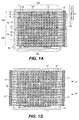
- a display device comprises a substrate 10 having a display area 11.
- a plurality of row electrodes 16 is formed over the substrate 10 in the display area 11 extending in a row direction and a plurality of column electrodes 12 are formed over the substrate 10 in the display area 11 extending in a column direction different from the row direction.
- the row and column electrodes 16, 12 overlap to form pixels 30.
- the row direction is orthogonal to the column direction and the pixels 30 form a regular array over the substrate 10.
- the pixels 30 are divided into two or more separate pixel groups 32, each pixel group 32 having group row electrodes 16A, 16B and separate group column electrodes 12A, 12B.
- separate group column electrodes is meant that the column electrodes of one pixel group are electrically isolated from the column electrodes of another pixel group.
- FIG. 1A the pixels 30 are divided into two pixel groups 32, one pixel group 32 in the upper half of the substrate 10 and the other pixel group 32 in the lower half of the substrate 10.
- the column electrodes 12 for each group are not electrically connected and each group of column electrodes only extends half of the way across the substrate 10 from the bottom to the top of FIG. 1A .
- Two or more spaced column driver chiplets 20 are located in the display area 11, at least one column driver chiplet 20 is located between at least one pixel of each of two different pixel groups 32 so that there are at least two pixel groups in the column direction and a column driver chiplet 20 between at least a portion of each of the two pixel groups so that at least one column driver chiplet 20 is not at the edge of the display area but within the display area with pixels surrounding it on each side.
- Each column driver chiplet 20 is uniquely connected to the group column electrodes 12 of one pixel group 32 and is adapted to drive the group column electrodes 12 of the one pixel group 32.
- One or more row driver(s) 21 are connected to the row electrodes 16.
- the row drivers 21 and the two or more spaced column driver chiplets 20 are adapted to drive the row and column electrodes 16, 12, respectively, to activate the pixels 30.
- a controller 40 is connected to the row drivers 21 and column driver chiplets 20 to provide image information and control signals.
- the row and column electrodes 16, 12 control the pixels 30.
- light-emitting material 14 for example, organic materials or inorganic quantum dot materials are located between the row and column electrodes 16, 12.
- a current passes from one electrode through the light-emitting material 14 in the pixel area 30 to the other electrode, light is emitted in proportion to the current density in the material, for example, as is the case with an organic light-emitting diode.
- the row and column electrodes 16, 12 can be formed in separate layers and each pixel group 32 can have passive-matrix control controlled by the row drivers 23 and column driver chiplets, 20.
- the pixels 30 formed by the overlap of the row and column electrodes 16, 12 are divided into pixel groups 32.
- At least two pixel groups are formed by separating the column electrodes 12 into two or more column electrode groups 12A, 12B in the column direction.
- two column electrodes 12 are present in each column over the substrate 10.
- a first group of column electrodes 12B extend from the bottom of the display 11 area to the middle of the display in the column direction.
- a second group of column electrodes 12A extends from the middle of the display to the top of the display in the column direction.
- Each of these two groups of column electrodes 12B, 12A form a separate pixel group 32 in the column direction and each of the pixel groups 32 is controlled by a separate column driver chiplet 20.
- the column driver chiplet 20 is located directly beneath the pixel group 32 that it controls.
- each pixel group 32 has a different set of row electrodes 16 driven by an external row driver 21.
- the designation "row” and "column" are arbitrary and can be exchanged.
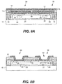
- FIG. 9 A more detailed illustration of the row and column electrodes 16, 12 is found in FIG. 9 .
- row electrodes 16 and column electrodes 12 formed on a substrate 10 overlap to form pixel areas 30 defining a pixel group 32.
- a column driver chiplet 20 electrically connects to the column electrodes 12 through connection pads 24 formed on the chiplet.
- the row driver chiplet 23 is electrically connected to the row electrodes 16 through connection pads 24 formed on the row driver chiplet 23.
- Cross sections 8A, 8A' and 8B, 8B' are illustrated in FIGS. 8A and 8B .
- FIG. 8A is a cross section of 8A, 8A' (in FIG. 9 ) of an embodiment of the device.
- a column driver chiplet 20 having a separate chiplet substrate 28 is adhered to a substrate 10 and buried with adhesion layer 18.
- the column driver chiplet 20 includes circuitry 22 and data value registers 26.
- Column electrodes 12 are electrically connected to connection pads 24 formed on the column driver chiplet 20.
- Light-emitting material 14 is located over the column electrodes 12 and row electrodes 16 formed over the light-emitting material 14. (A row electrode 16 is shown over the column driver chiplet 20 although the corresponding row electrode is omitted from FIG.
- the light-emitting material 14 can include multiple layers of light-emitting material as well as various charge-control layers as are known in the organic and inorganic light-emitting diode art.
- the electrodes 12, 16 and light-emitting material 14 form a light-emitting diode 15.
- FIG. 8B is a cross section of 8B, 8B' (in FIG. 9 ) of an embodiment of the device. Referring to FIG. 8B , a row driver chiplet 23 having a separate chiplet substrate 28 is adhered to a substrate 10 and buried with adhesion layer 18.
- the row driver chiplet 23 includes circuitry 22 and a rotary serial shift register 27. Row electrodes 16 are electrically connected to connection pads 24 formed on the chiplet 23.
- the areas overlapping both the column electrodes 12 and the row electrodes 16 in FIG. 8A form pixels 30 that can emit light when current is passed through the light-emitting material 14 from the row electrode 16 and column electrode 12 by the column driver chiplet 20 and row driver chiplet 23 through the connection pads 24 and controlled by the chiplet circuitry 22 in the column driver chiplet 20 and row driver chiplet 23.
- the present invention can be employed in both a top-emitter configuration and in a bottom emitter configuration.
- the chiplets are located in a layer beneath the row and column electrodes and occupy space over the substrate.
- a top-emitter configuration can be preferred so that the emitting area of the device is increased.
- a substrate 10 with display area 11 includes two pixel groups 32 and two column driver chiplets 20 controlling column electrodes 12.
- the row electrodes 16 of each pixel group 32 are driven in common with two external row drivers 21.
- the two external row drivers 21 drive the same row electrodes 16 with the same signal in parallel to provide additional current and reduce any voltage drop across the electrodes.
- the group row electrodes of one pixel group are driven in common by two or more row drivers.
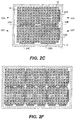
- a substrate 10 with display area 11 includes four pixel groups 32A, 32B, 32C, 32D and four column driver chiplets 20A, 20B, 20C, 20D controlling column electrodes 12 in each of the four pixel groups.
- two external row drivers 21 drive row electrodes 16 from either side of the substrate 10.
- the row electrodes 16 of pixel groups 32A and 32B are driven in common with the same signal
- the row electrodes 16 of pixel groups 32C and 32D are driven in common with the same signal.
- the group row electrodes of one pixel group are driven in common by two or more row drivers.
- the column driver chiplet 20A must be synchronized with column driver chiplet 20B and the column driver chiplet 20C must be synchronized with column driver chiplet 20D.
- two or more separate pixel groups have group row electrodes in common and the common group row electrodes are driven in common by two or more row drivers.
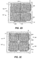
- a substrate 10 with display area 11 includes four pixel groups 32A, 32B, 32C, 32D and four column driver chiplets 20A, 20B, 20C, 20D controlling separate column electrodes 12 in each of the four pixel groups 32A, 32B, 32C, 32D.
- each of the pixel groups 32A, 32B, 32C, 32D has separate row electrodes 16 electrically connected to a separate external row driver 21.
- all of the row electrodes 16 and column electrodes 12 of each pixel group 32A, 32B, 32C, 32D are electrically separate, and each pixel group 32A, 32B, 32C, 32D is controlled independently of any other pixel groups.
- FIG. 1A-1D employ row drivers 21 external to the display area 11.
- row electrodes are correspondingly long, and even if the row electrodes are divided in half, as shown in the embodiment of FIG. 1D or the row electrodes 16 are driven from each side of the display area by two row drivers 21, as in the embodiment of FIGS. 1B and 1C , the potential voltage drop along the row electrodes 12 and capacitance of the row electrodes can significantly limit the overall performance of the device.
- row drivers are implemented as chiplets and located within the display area as are the column driver chiplets.
- a device has four pixel groups 32A, 32B, 32C, 32D formed on a substrate 10 within display area 11, each pixel group 32A, 32B, 32C, 32D having separate group row and group column electrodes 16, 12 and a separate column driver chiplet 20A, 20B, 20C, 20D and a separate row driver chiplet 23A, 23B, 23C, 23D.
- each pixel group 32A, 32B, 32C, 32D can operate independently from any other pixel group.
- the row and column driver chiplets 23A, 23B, 23C, 23D, 20A, 20B, 20C, 20D are located in the display area 11 and, in the figure, the column driver chiplets 20A, 20B, 20C, 20D drive the pixel groups 32A, 32B, 32C, 32D above the column driver chiplets 20A, 20B, 20C, 20D while the row driver chiplets 23A, 23B, 23C, 23D drives the pixel groups 32A, 32B, 32C, 32D to the left of the row driver chiplets 23A, 23B, 23C, 23D
- pixel group 32A is controlled by column driver chiplet 20A and row driver chiplet 23A.
- Pixel group 32B is controlled by column driver chiplet 20B and row driver chiplet 23B.
- Pixel group 32C is controlled by column driver chiplet 20C and row driver chiplet 23C.
- Pixel group 32D is controlled by column driver chiplet 20D and row driver chiplet 23D.
- the number of column electrodes 16 controlled by the column driver chiplet can differ from the number of row electrodes 12 controlled by the row driver chiplet.
- the row driver chiplets 23A, 23B, 23C, 23D and the column driver chiplets 20A, 20B, 20C, 20D can thus be of different sizes or have a different number of connection pads or drive a different number of electrodes.
- a device has four pixel groups 32A, 32B, 32C, 32D formed on a substrate 10 within display area 11, each pixel group 32A, 32B, 32C, 32D having separate group column electrodes 16 and a separate column driver chiplet 20A, 20B, 20C, 20D respectively.
- the row electrodes 12 in the same row are shared between multiple pixel groups and are driven in common with the same signal by multiple row driver chiplets.
- Each row electrode 16 is electrically continuous across pixel group 32A and 32B.
- each row electrode 16 is electrically continuous across pixel group 32C and 32D.
- the row and column driver chiplets are located in the display area 11 and in the figure, each column driver chiplet drives the pixel group located directly above it.
- FIG. 2B differs from FIG. 2A in that the row electrodes are shared between horizontally adjacent pixel group pairs.
- pixel group 32A is controlled by column driver chiplet 20A and row driver chiplets 23A and 23B.
- Pixel group 32B is controlled by column driver chiplet 20B and row driver chiplets 23A and 23B.
- Pixel group 32C is controlled by column driver chiplet 20C and row driver chiplets 23C and 32D.
- Pixel group 32D is controlled by column driver chiplet 20D and row driver chiplets 23C and 23D.
- row driver chiplets 23A and 23B must output the same signals and row driver chiplets 23C and 23D must output the same signals.
- column driver chiplet 20A must be coordinated with column driver chiplet 20B and column driver chiplet 20C must be coordinated with column driver chiplet 20D so that image information is properly displayed on the right rows.
- Using two row driver chiplets in parallel with electrically common row electrodes can improve the distribution of current in the row electrodes between the pixel groups (e.g. 32A and 32B or 32C and 32D) sharing the row electrodes.
- a device has four pixel groups 32A, 32B, 32C, 32D formed on a substrate 10 within display area 11, each pixel group 32A, 32B, 32C, 32D having separate group column electrodes 16 and a separate column driver chiplet 20A, 20B, 20C, 20D respectively.
- the row electrodes 12, however, are shared between multiple pixel groups and are driven in common by a single row driver chiplet.
- the row and column driver chiplets 23A, 23B, 20A, 20B, 20C, 20D are located in the display area 11 and, in the figure, the column driver chiplets 20A, 20B, 20C, 20D each drive the pixel group above it while each row driver chiplet drives the row electrodes to its left.
- FIG. 2C differs from FIG. 2B in that only one row driver chiplet drives the row electrodes.
- pixel group 32A is controlled by column driver chiplet 20A and row driver chiplet 23A.
- Pixel group 32B is controlled by column driver chiplet 20B and row driver chiplet 23A.
- Pixel group 32C is controlled by column driver chiplet 20C and row driver chiplet 23B.
- Pixel group 32D is controlled by column driver chiplet 20D and row driver chiplet 23B.
- column driver chiplets 20A and 20B must be coordinated and column driver chiplets 20C and 20D must be coordinated. Using a single row driver chiplet reduces the number of row driver chiplets.
- a device has two pixel groups, 32A and 32B, formed on a substrate 10 within display area 11, each pixel group 32A, 32B having separate group row electrodes 16 and a separate column driver chiplet 20A, 20B respectively.
- the row electrodes 16 are unique to each pixel group 32A, 32B.
- the row electrodes 16 of each group are driven in common by two independent row driver chiplets.
- pixel group 32A is controlled by column driver chiplet 20A and row driver chiplet 23A and 23B.
- Pixel group 32B is controlled by column driver chiplet 20B and row driver chiplets 23C and 23D. Using multiple row driver chiplet for row electrodes improves the current distribution in the electrodes.
- a device has four pixel groups 32A, 32B, 32C, 32D formed on a substrate 10 within display area 11, each pixel group 32A, 32B, 32C, 32D having separate group column electrodes 16 and separate row driver electrodes 12.
- Each pixel group 32A, 32B, 32C, 32D has a separate column driver chiplet and a separate row driver chiplet.
- the row driver comprises two electrically-connected chiplets.
- the row driver for pixel group 32B for example, comprises chiplet 23B1 and chiplet 23B2.
- the row driver for pixel group 32D for example, comprises chiplet 23D1 and chiplet 23D2.
- the chiplet pairs act together to control the group row electrodes of one pixel group by shifting the row enable signal from one chiplet to the next. While the illustration shows two chiplets, in other embodiments of the present invention, three, four, or more chiplets can be connected in series to form a single rotary serial shift register.
- Pixel groups 32A and 32C also have row drivers comprising two chiplets. This can be useful, for example, if the number of pixels defined by a column electrode supported by a column driver chiplet is greater than the number of row electrodes that can be supported by a single row driver chiplet.
- FIG. 2F illustrates an embodiment of the present invention having 12 pixel groups 32A-32L.
- the pixel groups are arranged in pairs (e.g. 32A, 32B) having common row electrodes and a common row driver chiplet.
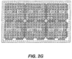
- FIG. 2G illustrates an embodiment of the present invention having 12 pixel groups 32A-32L.
- the group row electrodes of pixel groups 32A-32F are electrically common as are the group row electrodes of pixel groups 32G-32L.
- Each row driver comprises two chiplets forming a single rotary serial shift register. Pairs of pixel groups share a row driver.
- the number of column driver and row driver chiplets will be determined at least by the electrical characteristics of the chiplets, the characteristics of the row and column electrodes, the size of the pixel elements formed by the overlap of the row and column electrodes, and the rate (frequency) at which the pixels are driven with data.
- FIGS. 2B , 2C , and 2D illustrate various embodiments of the present invention in which the number of pixel groups supported by each row driver chiplet varies.
- the number of row and column driver chiplets can be chosen depending on the acceptable electrical characteristics of the device.
- the number of column electrodes supported by a column driver chiplet is also limited by the number of connection pads and the amount of circuitry that can be constructed in the column driver chiplet.
- the number of row electrodes supported by a row river chiplet is limited by the number of connection pads and the amount of circuitry that can be constructed in the row driver chiplet.
- the number of row and column chiplets is also limited by the necessary refresh rate for a signal displayed on the device. If a higher refresh rate is required, then the number of row and column driver chiplets is increased. If a lower refresh rate is required, then the number of row and column driver chiplets is decreased.
- FIG. 10 is an alternative top-view illustration of four pixel groups 32A, 32B, 32C, 32D, each pixel group having independent row electrodes 16 and column electrodes 12 and separate column driver chiplets 20A, 20B, 20C, 20D and row driver chiplets 23A, 23B, 23C, 23D.
- Chiplet connection pads 24 are indicated but no-connection wires between the chiplets or the connection pads and electrodes.
- pixel group 32A is controlled by column controller 20A and row controller 23A
- Pixel group 32B is controlled by column controller 20B and row controller 23B.
- Pixel group 32C is controlled by column controller 20C and row controller 23C.
- Pixel group 32D is controlled by column controller 20D and row controller 23D.
- the relative locations of the chiplets within a pixel group or over the substrate is not critical, so long as the group column electrodes are properly connected to the corresponding column driver chiplet and the group row electrodes are properly connected to the corresponding row driver chiplet.
- a chiplet connected to 16 electrodes has been constructed. It has also been calculated that a row driver chiplet can support the current from 128 columns.
- a display device that has 480 rows and 640 columns with three colors has 921,600 light-emitting elements. In a stripe configuration, this equals 1,920 columns and 480 rows.
- 120 column driver chiplets (each supporting 16 electrodes) are required in the row direction. At least 30 row driver chiplets (each supporting 16 electrodes) are necessary in the column direction. Therefore, 3600 column driver chiplets are required (120 x 30) and 450 row driver chiplets (30 by 1920/128) for a total of 4050 chiplets.
- the column driver chiplets must drive longer wires and control more pixels, but fewer chiplets need be employed. For example, if the rotary serial shift register controls 64 rows with two chiplets having 32 electrode connections each, only 5120 chiplets are needed (4096 column driver chiplets and 1024 row driver chiplets), but the pixel groups are twice as large.
- any pixel array controlled by scanning rows flicker is a concern.
- passive-matrix display devices are limited to approximately 100 rows. If more rows than that are included, the drivers cannot cycle through the rows fast enough to prevent perceptible flicker.
- the present invention provides advantages in that the electrode lengths are greatly reduced so that the electrodes can be controlled at a much faster rate.
- multiple rows can be simultaneously enabled, greatly reducing the number of rows that are sequentially driven. Therefore, using the present invention, very large pixel arrays can be constructed that provide superior image quality. Since no active-matrix thin-film transistors need to be constructed on the substrate (typically at high temperatures), manufacturing costs can be greatly reduced and a wider variety of substrate materials employed, for example flexible, plastic substrates.
- the row drivers include a rotary serial shift register for selecting a single row electrode at one time.
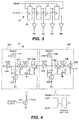
- FIG. 3 a simplified circuit diagram illustrates a mechanism for controlling four rows in a row driver.
- the row drivers include a reset circuit responsive to a reset signal to enable a single row and a shifting circuit that receives a row select signal to progressively and uniquely enable a single row.
- a series of four shift registers 29 are connected so that, with the application of a row select signal (equivalent to a shift register clock) to all of the shift registers 29, the data in each shift register is shifted to the next, serially-connected shift register 29; the data in the last shift register 29 is transferred to the first.
- the circuit provides a rotary, serial shift register 27.
- the reset signal sets all of the shift registers to a zero except the first, which is set to one.
- the shift register 29 having a one enables the corresponding row (R1, R2, R3, R4) so that, as the one value shifts through the rotary, serial shift register 27, each row is progressively enabled and only one row R1, R2, R3, R4 is enabled at a time.
- enable and disable signals can be either high or low, 0 or 1, and the signal levels described herein can be exchanged.
- the reset signal may be periodically employed to set the shift register to the same state as would occur when the data value in the last shift register is shifted to the first.
- the electrical connection from the last shift register to the first shift register may be omitted (and is therefore shown as a dashed line), thereby reducing the wiring complexity of the row driver.
- This arrangement is particularly useful when multiple chiplets are employed to form the rotary serial shift register since, in that case, the omitted electrical connection from the last shift register to the first would have to be routed outside the chiplets and over the substrate.
- the multiple-chiplet rotary serial shift register embodiment it is useful to set only the first register of the first chiplet in the connected series of chiplets comprising the rotary serial shift register to an enable value.
- the remainder of the chiplets can set the first register within the chiplet to a disable value.
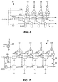
- each shift register includes two capacitors (e.g. 61A, 62A) and four transistors (e.g. 52A, 53A, 54A, 55A) forming a serial shifting circuit.
- a reset transistor forming a reset circuit is employed to reset the circuit and drive a row electrode.
- the reset signal is then returned to zero and clk2 enabled (disabling clk1).
- the signal provided to the shift register 29B through transistor 56B then charges the capacitor 61B and turns on the transistor 52B.
- signal D drains the capacitor 61A through transistor 56A and turns off transistor 52A.
- clk1 is subsequently enabled and clk2 disabled, the value stored in the first capacitor 61B is transferred to the second capacitor 62B, thus performing a complete data shift from one shift register 29A to the next 29B.
- Row R1 is then disabled and row R2 enabled.
- the embodiment of Fig. 4 illustrates a rotary serial shift register 27 with a double-buffered registers 29A, 29B shifted with a multi-phase clock signal.
- FIG. 4 illustrates a rotary serial shift register 27 with a double-buffered registers 29A, 29B shifted with a multi-phase clock signal.
- FIG. 5 illustrates the same circuit with four serially connected double-buffered, multi-phase shift registers 29 comprising a rotary serial shift register.
- the circuit can be extended with more shift registers 29 to support as many rows as desired and can fit into a row driver chiplet, or series of row driver chiplets.
- the rotary serially connected shift register can pass data into another chiplet to make the shift register as long as is desired, so long as the end register is connected to an input on the first register (see FIG. 2E ).
- the column driver chiplet circuit 20 include two data value registers 26, each data value register 26 storing at least as many analog data values as there are columns in the pixel group to which the column driver chiplet is connected.
- four data value registers are illustrated for a chiplet that can control four column electrodes.
- the data value registers 26 are serial registers and data values are stored in the serial data value registers 26 by shifting data into the registers 26, controlled by a clock signal. A select signal controls into which data value register 26 the data is transferred and to which column electrode driver the data is presented.
- FIG. 7 A more detailed circuit diagram of a circuit useful for a column driver chiplet 20 is illustrated in FIG. 7 .
- Two serially-connected analog shift registers are controlled by a clock signal.
- Analog shift registers are known in the art and employed for example in both CCD and CMOS imagers. They typically employ a multi-phase clock to shift analog values (represented by charges in a capacitor or semiconductor well) from one register to the next.
- a select signal and its inverse select the data value register into which the analog data is shifted through transistors 70.
- select transistors 72 present the analog data values in each data value register to a column electrode driver to drive the column electrodes C1, C2, C3, C4 in a pixel group.
- the column driver chiplets can be serially connected so that an entire row of data values can be shifted through the data value registers that are not selected, the select signal switched so that the data in the data value register is selected for output to the column electrodes, and the other data value register loaded with data using the clock signal. In this way, data values are alternately loaded and driven onto the column electrodes in a simple and efficient manner.
- the signal used to select the data in the column driver chiplet data value register 26 is the same signal as can be employed to shift the row driver rotary serial shift register 27.
- a column driver chiplet circuit 20 can alternately select the data output from two serial shift registers 27.
- one serial shift register 27 can be employed to shift data into the chiplet and a register used to store the shifted data upon the application of a select signal. The stored data can then be used to control the column electrodes while the next set of data are shifted into the serial shift register. This embodiment has the advantage of reducing the amount of circuitry required in the chiplet.
- the present invention provides reduced costs over the prior art.
- Conventional, active-matrix backplanes employ relatively low-performance and expensive thin-film semiconductor materials.
- the row driver chiplets need not have the same number of connection pads, or the same layout of connection pads. Moreover, the number of rows that the row driver chiplets drive need not be the same as the number of columns that the column driver chiplets drive.
- the row driver and column driver chiplets can be located in a wide variety of locations, so long as they are electrically connected to the corresponding row or column electrodes. Locations are generally selected to provide routing paths for electrical connections to chiplets and to space the chiplets from each other at a required positional tolerance suitable for the manufacturing process employed.
- row driver chiplets can be different from the technology, processes, or construction of column driver chiplets.
- construction is meant the process limitations, materials, and manufacturing processes employed to construct the row and column driver chiplets.
- one chiplet can employ digital designs, processes, and materials while the other employs analog.
- one chiplet can employ relatively high-voltage designs, processes, and materials while the other employs relatively low-voltage.
- one chiplet can employ semiconductor substrate materials or doping (e.g. n- or p-doping) while the other employs different materials or doping.
- the chiplets can also employ different circuit schematics.
- the chiplet controlling the independent drive direction requires circuitry to receive image data, requires one or more memory locations for image data per output, and controls relatively small currents and functions better when implemented with smaller line-width semiconductor processes.
- the chiplet controlling the common drive direction does not receive image data or require image data memory, but is required to switch relatively large currents and therefore functions better when implemented with wider line-width semiconductor processes.
- the chiplet connection pads 24 can be directly connected to a row or column electrode 16, 12. However, such connections can cause the chiplets to be larger than necessary.
- the chiplets can be aligned in any orientation with respect to the pixel groups and substrate, including aligning an edge of a chiplet with a row or column electrode. Indeed, different chiplets can be differently aligned.
- a display device can include a plurality of row driver chiplets and a separate plurality of column driver chiplets distributed over the substrate, each chiplet having a long dimension and a short dimension, the long dimension of the row driver chiplet orthogonal to the long dimension of the column driver chiplet.
- Chiplets can be rectangular, with two opposite sides of the rectangle being longer than the other two opposite sides, defining a chiplet with a large aspect ratio having long sides and short sides.
- a long side of a chiplet can be aligned in the same direction as row electrodes or column electrodes. For example, it can be helpful to align a long side of a row driver chiplet with column electrodes and a long side of a column electrode with row electrodes.
- Connection pads can be connected with wiring to the row electrodes. Vias can be employed to connect from one wiring layer to another or to connection pads and are formed between, for example, the column electrodes to avoid electrical shorts with the column electrodes. Since considerable wiring can be necessary to electrically connect the connection pads to the row and column electrodes, a top emitter configuration can be preferred, in which the top electrode is transparent and the bottom electrode can be reflective. The substrate can also be opaque.
- Chiplets may have a single row or multiple rows of connection pads 24 along a relatively long side of the chiplet longer than a relatively shorter neighboring side.
- Circuitry in the row driver chiplets can be different from the circuitry in the column driver chiplets.
- row drivers can employ very simple circuits with lower data rates but may switch large currents compared to a column driver.
- the number of rows controlled by the row driver chiplet can be different from the number of columns driven by the column driver chiplet.
- different circuits can be used in the different drivers, or even different manufacturing processes or technologies employed to make the different drivers.
- the chiplets can be connected to an external controller through a buss or through multiple busses (not shown in the drawings, for clarity).
- the buss can be a serial, parallel, or point-to-point buss and can be digital or analog.
- a serial buss is one in which data is re-transmitted from one chiplet to the next on electrically separated electrical connections while a parallel buss is one in which data is simultaneously broadcast to all of the chiplets on an electrically common electrical connection.
- a buss is connected to the chiplets to provide signals, such as power, ground, data, or select signals. More than one buss separately connected to one or more controllers can be employed.
- a controller receives and processes an information signal according to the needs of the display device and transmits the processed signal and control information through one or more busses to each chiplet in the device.
- the processed signal includes luminance information for each light-emitting pixel element corresponding to the associated row and column driver chiplets.
- the luminance information can be stored in an analog or digital storage element corresponding to each light-emitting pixel element.
- the chiplets then sequentially activate the row and column electrodes to which they are connected. When both the row and column electrode for a pixel is activated, current can flow through the pixel defined by the row and column electrode to emit light.
- an entire group of row electrodes or group of column electrodes within a pixel group is activated simultaneously by activating all of the group column electrodes and one row electrode at once (or vice versa ).
- the column electrodes are controlled to provide the individual luminance desired for each pixel in the row.
- a second row is selected and the process repeats until all of the rows are activated and all of the pixels emit light. The process can then repeat.
- Separate pixel groups can function independently. Note that the designation of "row” and “column” is arbitrary and the functions of row and column electrodes can be reversed.
- the busses can supply a variety of signals, including timing (e.g. clock) signals, data signals, select signals, power connections, or ground connections.
- the signals can be analog or digital, for example digital addresses or data values. Analog data values can be supplied as charge.
- the storage registers can be digital (for example comprising flip-flops) or analog (for example comprising capacitors for storing charge).
- the row driver or column driver chiplets distributed over the substrate can be identical.
- a unique identifying value i.e. an ID
- the ID can be assigned before or, preferably, after the chiplet is located over the substrate and the ID can reflect the relative position of the chiplet on the substrate, that is, the ID can be an address.
- the ID can be assigned by passing a count signal from one chiplet to the next in a row or column. Separate row or column ID values can be used.
- the controller can be implemented as a chiplet and affixed to the substrate.
- the controller can be located on the periphery of the substrate, or can be external to the substrate and comprise a conventional integrated circuit.
- the chiplets can be constructed in a variety of ways, for example with one or two rows of connection pads along a long dimension of a chiplet.
- Interconnection busses and wires can be formed from various materials and use various methods for deposition on the device substrate.
- interconnection busses and wires can be metal, either evaporated or sputtered, for example aluminum or aluminum alloys.
- the interconnection busses and wires can be made of cured conductive inks or metal oxides.
- the interconnection busses and wires are formed in a single layer.
- the present invention is particularly useful for multi-pixel device embodiments employing a large device substrate, e.g. glass, plastic, or foil, with a plurality of chiplets arranged in a regular arrangement over the device substrate.
- a large device substrate e.g. glass, plastic, or foil
- Each chiplet can control a plurality of pixels formed over the device substrate 10 according to the circuitry in the chiplet and in response to control signals.
- Individual pixel groups or multiple pixel groups can be located on tiled elements, which can be assembled to form the entire display.
- chiplets provide distributed pixel control elements over a substrate.
- a chiplet is a relatively small integrated circuit compared to the device substrate and includes a circuit including wires, connection pads, passive components such as resistors or capacitors, or active components such as transistors or diodes, formed on an independent substrate.
- Chiplets are separately manufactured from the display substrate and then applied to the display substrate.
- the chiplets are preferably manufactured using silicon or silicon on insulator (SOI) wafers using known processes for fabricating semiconductor devices.
- SOI silicon on insulator
- the plurality of chiplets therefore has a corresponding plurality of substrates separate from the device substrate and each other.
- the independent substrates are separate from the substrate on which the pixels are formed and the areas of the independent, chiplet substrates, taken together, are smaller than the device substrate.
- Chiplets can have a crystalline substrate to provide higher performance active components than are found in, for example, thin-film amorphous or polycrystalline silicon devices.
- Chiplets can have a thickness preferably of 100 um or less, and more preferably 20 um or less. This facilitates formation of the adhesive and planarization material over the chiplet that can then be applied using conventional spin-coating techniques.
- chiplets formed on crystalline silicon substrates are arranged in a geometric array and adhered to a device substrate with adhesion or planarization materials. Connection pads on the surface of the chiplets are employed to connect each chiplet to signal wires, power busses and row or column electrodes to drive pixels. Chiplets can control at least four pixels.
- the circuitry of the chiplet can be formed using modern lithography tools. With such tools, feature sizes of 0.5 microns or less are readily available. For example, modem semiconductor fabrication lines can achieve line widths of 90 nm or 45 nm and can be employed in making the chiplets of the present invention.
- the chiplet also requires connection pads for making electrical connection to the wiring layer provided over the chiplets once assembled onto the display substrate.
- the connection pads must be sized based on the feature size of the lithography tools used on the display substrate (for example 5 um) and the alignment of the chiplets to the wiring layer (for example +/- 5um). Therefore, the connection pads can be, for example, 15 um wide with 5 um spaces between the pads. This means that the pads will generally be significantly larger than the transistor circuitry formed in the chiplet.
- the pads can generally be formed in a metallization layer on the chiplet over the transistors. It is desirable to make the chiplet with as small a surface area as possible to enable a low manufacturing cost.
- chiplets with independent substrates (e.g. comprising crystalline silicon) having circuitry with higher performance than circuits formed directly on the substrate (e.g. amorphous or polycrystalline silicon), a device with higher performance is provided. Since crystalline silicon has not only higher performance but much smaller active elements (e.g. transistors), the circuitry size is much reduced.
- a useful chiplet can also be formed using micro-electro-mechanical (MEMS) structures, for example as described in " A novel use of MEMs switches in driving AMOLED", by Yoon, Lee, Yang, and Jang, Digest of Technical Papers of the Society for Information Display, 2008, 3.4, p. 13 .
- MEMS micro-electro-mechanical
- the device substrate can comprise glass and the wiring layers made of evaporated or sputtered metal or metal alloys, e.g. aluminum or silver, formed over a planarization layer (e.g. resin) patterned with photolithographic techniques known in the art.
- the chiplets can be formed using conventional techniques well established in the integrated circuit industry.
- the present invention can be employed in devices having a multi-pixel infrastructure.
- the present invention can be practiced with LED devices, either organic or inorganic, and is particularly useful in information-display devices.
- the present invention is employed in a flat-panel OLED device composed of small-molecule or polymeric OLEDs as disclosed in, but not limited to U.S. Patent No. 4,769,292, issued September 6, 1988 to Tang et al. , and U.S. Patent No. 5,061,569, issued October 29, 1991 to VanSlyke et al.
- Inorganic devices for example, employing quantum dots formed in a polycrystalline semiconductor matrix (for example, as taught in US Publication 2007/0057263 by Kahen ), and employing organic or inorganic charge-control layers, or hybrid organic/inorganic devices can be employed.
- organic or inorganic light-emitting displays can be used to fabricate such a device, including active-matrix displays having either a top- or a bottom-emitter architecture.
Landscapes
- Engineering & Computer Science (AREA)
- Physics & Mathematics (AREA)
- Computer Hardware Design (AREA)
- General Physics & Mathematics (AREA)
- Theoretical Computer Science (AREA)
- Optics & Photonics (AREA)
- Control Of Indicators Other Than Cathode Ray Tubes (AREA)
- Control Of El Displays (AREA)
- Electroluminescent Light Sources (AREA)
Abstract
Description
- Reference is made to commonly-assigned
U.S. Patent Application Serial No. 12/372,132 filed February 17, 2009 - The present invention relates to display devices having a substrate with distributed, independent chiplets for controlling a pixel array.
- Flat-panel display devices are widely used in conjunction with computing devices, in portable devices, and for entertainment devices such as televisions. Such displays typically employ a plurality of pixels distributed over a substrate to display images. Each pixel incorporates several, differently colored light-emitting elements commonly referred to as sub-pixels, typically emitting red, green, and blue light to represent each image element. As used herein, pixels and sub-pixels are not distinguished and refer to a single light-emitting element. A variety of flat-panel display technologies are known, for example, plasma displays, liquid crystal displays, and light-emitting diode (LED) displays.
- Light emitting diodes (LEDs) incorporating thin films of light-emitting materials forming light-emitting elements have many advantages in a flat-panel display device and are useful in optical systems.
US Patent No. 6,384,529 issued May 7, 2002 to Tang et al. shows an organic LED (OLED) color display that includes an array of organic LED light-emitting elements. Alternatively, inorganic materials can be employed and can include phosphorescent crystals or quantum dots in a polycrystalline semiconductor matrix. Other thin films of organic or inorganic materials can also be employed to control charge injection, transport, or blocking to the light-emitting-thin-film materials, and are known in the art. The materials are placed upon a substrate between electrodes, with an encapsulating cover layer or plate. Light is emitted from a pixel when current passes through the light-emitting material. The frequency of the emitted light is dependent on the nature of the material used. In such a display, light can be emitted through the substrate (a bottom emitter) or through the encapsulating cover (a top emitter), or both. - LED devices can comprise a patterned light-emissive layer wherein different materials are employed in the pattern to emit different colors of light when current passes through the materials. Alternatively, one can employ a single emissive layer, for example, a white-light emitter, together with color filters for forming a full-color display, as is taught in
U.S. Patent 6,987,355 entitled, "Stacked OLED Display having Improved Efficiency" by Cok. It is also known to employ a white sub-pixel that does not include a color filter, for example, as taught inU.S. Patent 6,919,681 entitled, "Color OLED Display with Improved Power Efficiency" by Cok et al. A design employing an unpatterned white emitter has been proposed together with a four-color pixel comprising red, green, and blue color filters and sub-pixels and an unfiltered white sub-pixel to improve the efficiency of the device (see, e.g.U.S. Patent 7,230,594 issued June 12, 2007 to Miller, et al ). - Two different methods for controlling the pixels in a flat-panel display device are generally known: active-matrix control and passive-matrix control. In a passive-matrix device, the substrate does not include any active electronic elements (e.g. transistors). An array of row electrodes and an orthogonal array of column electrodes in a separate layer are formed over the substrate; the overlapping intersections between the row and column electrodes form the electrodes of a light-emitting diode. External driver chips then sequentially supply current to each row (or column) while the orthogonal column (or row) supplies a suitable voltage to illuminate each light-emitting diode in the row (or column). Therefore, a passive-matrix design employs 2n connections to produce n2 separately controllable light-emitting elements. However, a passive-matrix drive device is limited in the number of rows (or columns) that can be included in the device since the sequential nature of the row (or column) driving creates flicker. If too many rows are included, the flicker can become perceptible. Moreover, the currents necessary to drive an entire row (or column) in a display can be problematic since the power required for the non-imaging pre-charge and discharge steps of PM driving become dominant as the area of the PM display grows. These problems limit the physical size of a passive-matrix display.
- In an active-matrix device, active control elements are formed of thin films of semiconductor material, for example amorphous or poly-crystalline silicon, coated over the flat-panel substrate. Typically, each sub-pixel is controlled by one control element and each control element includes at least one transistor. For example, in a simple active-matrix organic light-emitting (OLED) display, each control element includes two transistors (a select transistor and a power transistor) and one capacitor for storing a charge specifying the luminance of the sub-pixel. Each light-emitting element typically employs an independent control electrode and an electrode electrically connected in common. Control of the light-emitting elements is typically provided through a data signal line, a select signal line, a power connection and a ground connection. Active-matrix elements are not necessarily limited to displays and can be distributed over a substrate and employed in other applications requiring spatially distributed control. The same number of external control lines (except for power and ground) can be employed in an active-matrix device as in a passive-matrix device. However, in an active-matrix device, each light-emitting element has a separate driving connection from a control circuit and is active even when not selected for data deposition so that flicker is eliminated.
- One common, prior-art method of forming active-matrix control elements typically deposits thin films of semiconductor materials, such as silicon, onto a glass substrate and then forms the semiconductor materials into transistors and capacitors through photolithographic processes. The thin-film silicon can be either amorphous or polycrystalline. Thin-film transistors (TFTs) made from amorphous or polycrystalline silicon are relatively large and have lower performance compared to conventional transistors made in crystalline silicon wafers. Moreover, such thin-film devices typically exhibit local or large-area non-uniformity across the glass substrate that results in non-uniformity in the electrical performance and visual appearance of displays employing such materials. In such active-matrix designs, each light-emitting element requires a separate connection to a driving circuit.
- Employing an alternative control technique, Matsumura et al describe crystalline silicon substrates used for driving LCD displays in
U.S. Patent Application 2006/0055864 . The application describes a method for selectively transferring and affixing pixel-control devices made from first semiconductor substrates onto a second planar display substrate. Wiring interconnections within the pixel-control device and connections from busses and control electrodes to the pixel-control device are shown. - Since a conventional passive-matrix display design is limited in size and number of light-emitting elements, and an active-matrix design using TFTs has lower electrical performance and complex substrates, there is a need for an improved control method for display devices that overcomes these problems.
- In accordance with the present invention, there is provided a display device, comprising:
- a) a substrate having a display area;
- b) a plurality of row electrodes formed over the substrate in the display area extending in a row direction and a plurality of column electrodes formed over the substrate in the display area extending in a column direction different from the row direction, the row and column electrodes overlapping to form pixels;
- c) wherein the pixels are divided into two or more separate pixel groups, each pixel group having group row electrodes and separate group column electrodes;
- d) two or more spaced column driver chiplets located in the display area, each column driver chiplet uniquely connected to a different pixel group wherein in at least one of the column driver chiplets is located between pixel groups, and the two or more spaced column driver chiplets adapted to drive the group column electrodes of the one pixel group;
- e) one or more row driver(s) connected to the row electrodes; and
- f) wherein the row drivers and the column driver chiplets cooperatively drive the row and column electrodes, respectively, to activate the pixels.
- The present invention has the advantage that, by providing a display device having a plurality of pixels divided into two or more separate pixel groups with chiplet column drivers located between pixel groups, performance is improved and the number of components and connections is reduced. Further, by having separate row and column driver chiplets, each chiplet can be made with the lowest cost semiconductor fabrication process available for each chiplet.
-
-
FIG. 1A is a plan view of a substrate with two pixel groups, two column driver chiplets, and an external row drivers according to an embodiment of the present invention; -
FIG. 1B is a plan view of a substrate with two pixel groups, two column driver chiplets, and two external row drivers according to an alternative embodiment of the present invention; -
FIG. 1C is a plan view of a substrate with four pixel groups, four column driver chiplets, and two external row drivers according to another embodiment of the present invention; -
FIG. 1D is a plan view of a substrate with four pixel groups, four column driver chiplets, two external row drivers, and separate row electrodes for each pixel group according to yet another embodiment of the present invention; -
FIG. 2A is a plan view of a substrate with four pixel groups, four column driver chiplets, four row driver chiplets, and separate row electrodes for each pixel group according to an embodiment of the present invention; -
FIG. 2B is a plan view of a substrate with four pixel groups, four column driver chiplets, four row driver chiplets, and shared row electrodes for pixel groups in a common row according to another embodiment of the present invention; -
FIG. 2C is a plan view of a substrate with four pixel groups, four column driver chiplets, two row driver chiplets, and shared row electrodes for pixel groups in a common row according to another embodiment of the present invention; -
FIG. 2D is a plan view of a substrate with two pixel groups, two column driver chiplets, and two row driver chiplets for each pixel group according to yet another embodiment of the present invention; -
FIG. 2E is a plan view of a substrate with four pixel groups, four column driver chiplets, eight row driver chiplets forming four row drivers, and separate row electrodes for each pixel group according to an embodiment of the present invention; -
FIG. 2F is a plan view of a substrate with twelve pixel groups, six row driver chiplets, with each row driver chiplet driving the rows of two pixel groups according to an embodiment of the present invention; -
FIG. 2G is a plan view of a substrate with twelve pixel groups, six pairs of row driver chiplets, with each row driver chiplet driving the rows of six pixel groups according to an embodiment of the present invention; -
FIG. 3 is a simplified schematic of row driver chiplet circuitry according to an embodiment of the present invention; -
FIG. 4 is a more detailed schematic of a portion of the row driver chiplet circuitry ofFIG. 3 according to an embodiment of the present invention; -
FIG. 5 is a more detailed schematic of the row driver chiplet circuitry ofFIG. 3 according to an embodiment of the present invention; -
FIG. 6 is a simplified schematic of column driver chiplet circuitry according to an embodiment of the present invention; -
FIG. 7 is a more detailed schematic of the row driver chiplet circuitry ofFIG. 6 according to an embodiment of the present invention; -
FIG. 8A is a partial cross section of a row driver chiplet according to an embodiment of the present invention; -
FIG. 8B is a partial cross section of a column driver chiplet according to an embodiment of the present invention; -
FIG. 9 is a plan view of a substrate portion with a pixel group, group row and column electrodes, a row driver chiplet, and a column driver chiplet according to an embodiment of the present invention; -
FIG. 10 is a plan view of a substrate portion with four pixel groups, group row and column electrodes, row driver chiplets, and column driver chiplets according to an embodiment of the present invention; and -
FIG. 11 is a plan view of a substrate portion with four pixel groups, group row and column electrodes, row driver chiplets, and column driver chiplets according to an embodiment of the present invention. - Because the various layers and elements in the drawings have greatly different sizes, the drawings are not to scale.
- Referring to
FIG. 1A , in one embodiment of the present invention, a display device comprises asubstrate 10 having adisplay area 11. A plurality ofrow electrodes 16 is formed over thesubstrate 10 in thedisplay area 11 extending in a row direction and a plurality ofcolumn electrodes 12 are formed over thesubstrate 10 in thedisplay area 11 extending in a column direction different from the row direction. The row andcolumn electrodes pixels 30. Typically, the row direction is orthogonal to the column direction and thepixels 30 form a regular array over thesubstrate 10. - The
pixels 30 are divided into two or moreseparate pixel groups 32, eachpixel group 32 havinggroup row electrodes 16A, 16B and separategroup column electrodes FIG. 1A , thepixels 30 are divided into twopixel groups 32, onepixel group 32 in the upper half of thesubstrate 10 and theother pixel group 32 in the lower half of thesubstrate 10. Thecolumn electrodes 12 for each group are not electrically connected and each group of column electrodes only extends half of the way across thesubstrate 10 from the bottom to the top ofFIG. 1A . - Two or more spaced
column driver chiplets 20 are located in thedisplay area 11, at least onecolumn driver chiplet 20 is located between at least one pixel of each of twodifferent pixel groups 32 so that there are at least two pixel groups in the column direction and acolumn driver chiplet 20 between at least a portion of each of the two pixel groups so that at least onecolumn driver chiplet 20 is not at the edge of the display area but within the display area with pixels surrounding it on each side. Eachcolumn driver chiplet 20 is uniquely connected to thegroup column electrodes 12 of onepixel group 32 and is adapted to drive thegroup column electrodes 12 of the onepixel group 32. One or more row driver(s) 21 are connected to therow electrodes 16. Therow drivers 21 and the two or more spacedcolumn driver chiplets 20 are adapted to drive the row andcolumn electrodes pixels 30. Acontroller 40 is connected to therow drivers 21 and column driver chiplets 20 to provide image information and control signals. - According to the present invention, the row and
column electrodes pixels 30. In one embodiment, (e.g.FIGS. 8A, 8B ) light-emittingmaterial 14, for example, organic materials or inorganic quantum dot materials are located between the row andcolumn electrodes material 14 in thepixel area 30 to the other electrode, light is emitted in proportion to the current density in the material, for example, as is the case with an organic light-emitting diode. - The row and
column electrodes pixel group 32 can have passive-matrix control controlled by therow drivers 23 and column driver chiplets, 20. According to the present invention, thepixels 30 formed by the overlap of the row andcolumn electrodes pixel groups 32. At least two pixel groups are formed by separating thecolumn electrodes 12 into two or morecolumn electrode groups FIG. 1A , twocolumn electrodes 12 are present in each column over thesubstrate 10. In the bottom half of the display area 11 a first group ofcolumn electrodes 12B extend from the bottom of thedisplay 11 area to the middle of the display in the column direction. A second group ofcolumn electrodes 12A extends from the middle of the display to the top of the display in the column direction. Each of these two groups ofcolumn electrodes separate pixel group 32 in the column direction and each of thepixel groups 32 is controlled by a separatecolumn driver chiplet 20. In the examples ofFIGS. 1A-1D (andFIGS. 2A-2G ), thecolumn driver chiplet 20 is located directly beneath thepixel group 32 that it controls. In the example ofFIG. 1A , eachpixel group 32 has a different set ofrow electrodes 16 driven by anexternal row driver 21. As used herein, the designation "row" and "column" are arbitrary and can be exchanged. - A more detailed illustration of the row and
column electrodes FIG. 9 . Referring toFIG. 9 ,row electrodes 16 andcolumn electrodes 12 formed on asubstrate 10 overlap to formpixel areas 30 defining apixel group 32. A column driver chiplet 20 electrically connects to thecolumn electrodes 12 throughconnection pads 24 formed on the chiplet. In this embodiment, therow driver chiplet 23 is electrically connected to therow electrodes 16 throughconnection pads 24 formed on therow driver chiplet 23.Cross sections FIGS. 8A and 8B . -
FIG. 8A is a cross section of 8A, 8A' (inFIG. 9 ) of an embodiment of the device. Referring toFIG. 8A , acolumn driver chiplet 20 having aseparate chiplet substrate 28 is adhered to asubstrate 10 and buried withadhesion layer 18. Thecolumn driver chiplet 20 includescircuitry 22 and data value registers 26.Column electrodes 12 are electrically connected toconnection pads 24 formed on thecolumn driver chiplet 20. Light-emittingmaterial 14 is located over thecolumn electrodes 12 androw electrodes 16 formed over the light-emittingmaterial 14. (Arow electrode 16 is shown over the column driver chiplet 20 although the corresponding row electrode is omitted fromFIG. 9 for clarity.) The light-emittingmaterial 14 can include multiple layers of light-emitting material as well as various charge-control layers as are known in the organic and inorganic light-emitting diode art. Theelectrodes material 14 form a light-emittingdiode 15.FIG. 8B is a cross section of 8B, 8B' (inFIG. 9 ) of an embodiment of the device. Referring toFIG. 8B , arow driver chiplet 23 having aseparate chiplet substrate 28 is adhered to asubstrate 10 and buried withadhesion layer 18. Therow driver chiplet 23 includescircuitry 22 and a rotaryserial shift register 27.Row electrodes 16 are electrically connected toconnection pads 24 formed on thechiplet 23. The areas overlapping both thecolumn electrodes 12 and therow electrodes 16 inFIG. 8A form pixels 30 that can emit light when current is passed through the light-emittingmaterial 14 from therow electrode 16 andcolumn electrode 12 by thecolumn driver chiplet 20 androw driver chiplet 23 through theconnection pads 24 and controlled by thechiplet circuitry 22 in thecolumn driver chiplet 20 androw driver chiplet 23. - The present invention can be employed in both a top-emitter configuration and in a bottom emitter configuration. However, as shown in
FIGS. 3A and8B , the chiplets are located in a layer beneath the row and column electrodes and occupy space over the substrate. Thus, a top-emitter configuration can be preferred so that the emitting area of the device is increased. - A variety of pixel groups with column driver chiplet and row driver arrangements are included within various embodiments of the present invention. Referring to
FIG. 1B in an alternative embodiment of the present invention, asubstrate 10 withdisplay area 11 includes twopixel groups 32 and two column driver chiplets 20 controllingcolumn electrodes 12. In this embodiment, however, therow electrodes 16 of eachpixel group 32 are driven in common with twoexternal row drivers 21. The twoexternal row drivers 21 drive thesame row electrodes 16 with the same signal in parallel to provide additional current and reduce any voltage drop across the electrodes. In this embodiment, the group row electrodes of one pixel group are driven in common by two or more row drivers. - Turning to
FIG. 1C in another embodiment of the present invention, asubstrate 10 withdisplay area 11 includes fourpixel groups column electrodes 12 in each of the four pixel groups. As in the embodiment ofFIG. 1B , twoexternal row drivers 21,drive row electrodes 16 from either side of thesubstrate 10. In this embodiment, therow electrodes 16 ofpixel groups row electrodes 16 ofpixel groups column driver chiplet 20A must be synchronized withcolumn driver chiplet 20B and thecolumn driver chiplet 20C must be synchronized withcolumn driver chiplet 20D. In this embodiment, two or more separate pixel groups have group row electrodes in common and the common group row electrodes are driven in common by two or more row drivers. - Referring to
FIG. 1D , asubstrate 10 withdisplay area 11 includes fourpixel groups separate column electrodes 12 in each of the fourpixel groups FIG. 1C , in the embodiment ofFIG. 1D each of thepixel groups separate row electrodes 16 electrically connected to a separateexternal row driver 21. In this embodiment, all of therow electrodes 16 andcolumn electrodes 12 of eachpixel group pixel group - The embodiments of
FIG. 1A-1D employ row drivers 21 external to thedisplay area 11. However, for large display devices, row electrodes are correspondingly long, and even if the row electrodes are divided in half, as shown in the embodiment ofFIG. 1D or therow electrodes 16 are driven from each side of the display area by tworow drivers 21, as in the embodiment ofFIGS. 1B and1C , the potential voltage drop along therow electrodes 12 and capacitance of the row electrodes can significantly limit the overall performance of the device. Hence, according to embodiments of the present invention, row drivers are implemented as chiplets and located within the display area as are the column driver chiplets. - Referring to
FIG. 2A in one embodiment, a device has fourpixel groups substrate 10 withindisplay area 11, eachpixel group group column electrodes column driver chiplet row driver chiplet pixel group display area 11 and, in the figure, the column driver chiplets 20A, 20B, 20C, 20D drive thepixel groups pixel groups pixel group 32A is controlled bycolumn driver chiplet 20A androw driver chiplet 23A.Pixel group 32B is controlled bycolumn driver chiplet 20B androw driver chiplet 23B.Pixel group 32C is controlled bycolumn driver chiplet 20C androw driver chiplet 23C.Pixel group 32D is controlled bycolumn driver chiplet 20D androw driver chiplet 23D. Note that the number ofcolumn electrodes 16 controlled by the column driver chiplet can differ from the number ofrow electrodes 12 controlled by the row driver chiplet. The row driver chiplets 23A, 23B, 23C, 23D and the column driver chiplets 20A, 20B, 20C, 20D can thus be of different sizes or have a different number of connection pads or drive a different number of electrodes. - Referring to
FIG. 2B in an alternative embodiment, a device has fourpixel groups substrate 10 withindisplay area 11, eachpixel group group column electrodes 16 and a separatecolumn driver chiplet row electrodes 12 in the same row, however, are shared between multiple pixel groups and are driven in common with the same signal by multiple row driver chiplets. Eachrow electrode 16 is electrically continuous acrosspixel group row electrode 16 is electrically continuous acrosspixel group display area 11 and in the figure, each column driver chiplet drives the pixel group located directly above it.FIG. 2B differs fromFIG. 2A in that the row electrodes are shared between horizontally adjacent pixel group pairs. For example,pixel group 32A is controlled bycolumn driver chiplet 20A androw driver chiplets Pixel group 32B is controlled bycolumn driver chiplet 20B androw driver chiplets Pixel group 32C is controlled bycolumn driver chiplet 20C androw driver chiplets Pixel group 32D is controlled bycolumn driver chiplet 20D androw driver chiplets row driver chiplets row driver chiplets column driver chiplet 20A must be coordinated withcolumn driver chiplet 20B andcolumn driver chiplet 20C must be coordinated withcolumn driver chiplet 20D so that image information is properly displayed on the right rows. Using two row driver chiplets in parallel with electrically common row electrodes can improve the distribution of current in the row electrodes between the pixel groups (e.g. 32A and 32B or 32C and 32D) sharing the row electrodes. - Referring to
FIG. 2C in another embodiment of the present invention, a device has fourpixel groups substrate 10 withindisplay area 11, eachpixel group group column electrodes 16 and a separatecolumn driver chiplet row electrodes 12, however, are shared between multiple pixel groups and are driven in common by a single row driver chiplet. The row and column driver chiplets 23A, 23B, 20A, 20B, 20C, 20D are located in thedisplay area 11 and, in the figure, the column driver chiplets 20A, 20B, 20C, 20D each drive the pixel group above it while each row driver chiplet drives the row electrodes to its left.FIG. 2C differs fromFIG. 2B in that only one row driver chiplet drives the row electrodes. For example,pixel group 32A is controlled bycolumn driver chiplet 20A androw driver chiplet 23A.Pixel group 32B is controlled bycolumn driver chiplet 20B androw driver chiplet 23A.Pixel group 32C is controlled bycolumn driver chiplet 20C androw driver chiplet 23B.Pixel group 32D is controlled bycolumn driver chiplet 20D androw driver chiplet 23B. In this embodiment, column driver chiplets 20A and 20B must be coordinated and column driver chiplets 20C and 20D must be coordinated. Using a single row driver chiplet reduces the number of row driver chiplets. - Turning to
FIG. 2D in another embodiment of the present invention, a device has two pixel groups, 32A and 32B, formed on asubstrate 10 withindisplay area 11, eachpixel group group row electrodes 16 and a separatecolumn driver chiplet row electrodes 16 are unique to eachpixel group row electrodes 16 of each group are driven in common by two independent row driver chiplets. For example,pixel group 32A is controlled bycolumn driver chiplet 20A androw driver chiplet Pixel group 32B is controlled bycolumn driver chiplet 20B androw driver chiplets - Referring to
FIG. 2E in another embodiment of the present invention, a device has fourpixel groups substrate 10 withindisplay area 11, eachpixel group group column electrodes 16 and separaterow driver electrodes 12. Eachpixel group pixel group 32B, for example, comprises chiplet 23B1 and chiplet 23B2. Similarly, the row driver forpixel group 32D, for example, comprises chiplet 23D1 and chiplet 23D2. The chiplet pairs act together to control the group row electrodes of one pixel group by shifting the row enable signal from one chiplet to the next. While the illustration shows two chiplets, in other embodiments of the present invention, three, four, or more chiplets can be connected in series to form a single rotary serial shift register.Pixel groups row electrodes 12 in a pixel group, the number of pixel groups and column driver chiplets is decreased. -
FIG. 2F illustrates an embodiment of the present invention having 12pixel groups 32A-32L. The pixel groups are arranged in pairs (e.g. 32A, 32B) having common row electrodes and a common row driver chiplet.FIG. 2G illustrates an embodiment of the present invention having 12pixel groups 32A-32L. The group row electrodes ofpixel groups 32A-32F are electrically common as are the group row electrodes ofpixel groups 32G-32L. Each row driver comprises two chiplets forming a single rotary serial shift register. Pairs of pixel groups share a row driver. Thus three chiplets comprising half of a rotary serial shift register drive half of the row electrodes in common forpixel groups 32A-32F while three chiplets comprising the other half of the rotary serial shift register drive the remaining half of the row electrodes in common forpixel groups 32A-32F.Pixel groups 32G-32L are driven likewise. This arrangement has the advantage of providing superior current distribution in the row electrodes and reducing the number of column driver chiplets. Similar arrangements having more or fewer column driver chiplets and more or fewer chiplets comprising each rotary serial shift registers are included within the present invention. The number of column driver and row driver chiplets will be determined at least by the electrical characteristics of the chiplets, the characteristics of the row and column electrodes, the size of the pixel elements formed by the overlap of the row and column electrodes, and the rate (frequency) at which the pixels are driven with data. -
FIGS. 2B ,2C , and2D illustrate various embodiments of the present invention in which the number of pixel groups supported by each row driver chiplet varies. In general, it is useful to determine the number of row and column driver chiplets in a device by evaluating the row and column electrode capacitance and voltage drop for a specific device. The number of row and column driver chiplets can be chosen depending on the acceptable electrical characteristics of the device. The number of column electrodes supported by a column driver chiplet is also limited by the number of connection pads and the amount of circuitry that can be constructed in the column driver chiplet. Likewise, the number of row electrodes supported by a row river chiplet is limited by the number of connection pads and the amount of circuitry that can be constructed in the row driver chiplet. The number of row and column chiplets is also limited by the necessary refresh rate for a signal displayed on the device. If a higher refresh rate is required, then the number of row and column driver chiplets is increased. If a lower refresh rate is required, then the number of row and column driver chiplets is decreased. -
FIG. 10 is an alternative top-view illustration of fourpixel groups independent row electrodes 16 andcolumn electrodes 12 and separate column driver chiplets 20A, 20B, 20C, 20D and row driver chiplets 23A, 23B, 23C, 23D.Chiplet connection pads 24 are indicated but no-connection wires between the chiplets or the connection pads and electrodes. In this illustration,pixel group 32A is controlled bycolumn controller 20A androw controller 23A Pixel group 32B is controlled bycolumn controller 20B androw controller 23B.Pixel group 32C is controlled bycolumn controller 20C androw controller 23C.Pixel group 32D is controlled bycolumn controller 20D androw controller 23D. The relative locations of the chiplets within a pixel group or over the substrate is not critical, so long as the group column electrodes are properly connected to the corresponding column driver chiplet and the group row electrodes are properly connected to the corresponding row driver chiplet. - For example, a chiplet connected to 16 electrodes has been constructed. It has also been calculated that a row driver chiplet can support the current from 128 columns. A display device that has 480 rows and 640 columns with three colors has 921,600 light-emitting elements. In a stripe configuration, this equals 1,920 columns and 480 rows. Hence, 120 column driver chiplets (each supporting 16 electrodes) are required in the row direction. At least 30 row driver chiplets (each supporting 16 electrodes) are necessary in the column direction. Therefore, 3600 column driver chiplets are required (120 x 30) and 450 row driver chiplets (30 by 1920/128) for a total of 4050 chiplets. In a larger device design using 32 electrode connections per chiplet for a high-definition device (presumed to be 2048 by 1024 for simplicity) with four-element (RGBW) pixels, an array of 8192 by 1024 light-emitting elements must be controlled. To support this design, 256 column driver chiplets are necessary (2048 x 4 / 32) across the width of the device and 32 row driver chiplets are required (1024 / 32) across the height of the device. Therefore, 8192 column driver chiplets are necessary (256 x 32) Assuming that each row driver chiplets can support 256 columns, 1024 row driver chiplets are required (8192 x 32 / 256) for a total of 9216 chiplets. If a rotary serial shift register comprising two chiplets (e.g. as in
FIG. 2E ) is employed, the column driver chiplets must drive longer wires and control more pixels, but fewer chiplets need be employed. For example, if the rotary serial shift register controls 64 rows with two chiplets having 32 electrode connections each, only 5120 chiplets are needed (4096 column driver chiplets and 1024 row driver chiplets), but the pixel groups are twice as large. - In any pixel array controlled by scanning rows, flicker is a concern. Typically, passive-matrix display devices are limited to approximately 100 rows. If more rows than that are included, the drivers cannot cycle through the rows fast enough to prevent perceptible flicker. In contrast, the present invention provides advantages in that the electrode lengths are greatly reduced so that the electrodes can be controlled at a much faster rate. Furthermore, by forming separately controlled pixel groups, multiple rows can be simultaneously enabled, greatly reducing the number of rows that are sequentially driven. Therefore, using the present invention, very large pixel arrays can be constructed that provide superior image quality. Since no active-matrix thin-film transistors need to be constructed on the substrate (typically at high temperatures), manufacturing costs can be greatly reduced and a wider variety of substrate materials employed, for example flexible, plastic substrates.
- In an embodiment of the present invention, the row drivers include a rotary serial shift register for selecting a single row electrode at one time. Referring to
FIG. 3 , a simplified circuit diagram illustrates a mechanism for controlling four rows in a row driver. The row drivers include a reset circuit responsive to a reset signal to enable a single row and a shifting circuit that receives a row select signal to progressively and uniquely enable a single row. A series of fourshift registers 29 are connected so that, with the application of a row select signal (equivalent to a shift register clock) to all of the shift registers 29, the data in each shift register is shifted to the next, serially-connectedshift register 29; the data in thelast shift register 29 is transferred to the first. Hence, the circuit provides a rotary,serial shift register 27. The reset signal sets all of the shift registers to a zero except the first, which is set to one. Theshift register 29 having a one enables the corresponding row (R1, R2, R3, R4) so that, as the one value shifts through the rotary,serial shift register 27, each row is progressively enabled and only one row R1, R2, R3, R4 is enabled at a time. (As is known in the art, enable and disable signals can be either high or low, 0 or 1, and the signal levels described herein can be exchanged.) - Although the output of the last shift register in the series is connected to the input of the first shift register in the series, the present invention is not limited to that embodiment. For example, the reset signal may be periodically employed to set the shift register to the same state as would occur when the data value in the last shift register is shifted to the first. By periodically employing the reset signal, the electrical connection from the last shift register to the first shift register may be omitted (and is therefore shown as a dashed line), thereby reducing the wiring complexity of the row driver. This arrangement is particularly useful when multiple chiplets are employed to form the rotary serial shift register since, in that case, the omitted electrical connection from the last shift register to the first would have to be routed outside the chiplets and over the substrate. Furthermore, in the multiple-chiplet rotary serial shift register embodiment, it is useful to set only the first register of the first chiplet in the connected series of chiplets comprising the rotary serial shift register to an enable value. The remainder of the chiplets can set the first register within the chiplet to a disable value.
- Referring to
FIG. 4 , in a more detailed embodiment of the circuit shown inFIG. 3 , and according to an embodiment of the present invention, two serially-connectedshift registers shift registers 29 inFIG. 3 ). The output of thesecond shift register 29B is connected to thefirst shift register 29A (as indicated with connection D). A two-phase clock is employed with the timing diagram indicated. Each shift register (e.g. 29A) includes two capacitors (e.g. 61A, 62A) and four transistors (e.g. 52A, 53A, 54A, 55A) forming a serial shifting circuit. A reset transistor forming a reset circuit is employed to reset the circuit and drive a row electrode. When a reset signal is applied totransistor 51A when clk1 is high and clk2 is low (clk1 is the inverse of clk2), the first capacitor 61 A is charged,transistor 52A is turned on,second capacitor 62A is charged andtransistor 53A, is turned on, providing a high signal to shiftregister 29B. The row-controllingtransistor 55A is also turned on to uniquely enable row R1. When the same reset signal is applied toshift register 29B throughtransistor 51B, thecapacitors transistor 53B is turned on, and transistors (52B, 54B) are pulled low so that the row-controlling transistor (55B) turns off row R2 and signal D is set low. (The same reset circuit can be used to setfirst shift register 29A to a low value in a multi-chiplet embodiment of the rotary serial shift register.) - The reset signal is then returned to zero and clk2 enabled (disabling clk1). The signal provided to the
shift register 29B throughtransistor 56B then charges thecapacitor 61B and turns on thetransistor 52B. In contrast, signal D drains the capacitor 61A throughtransistor 56A and turns offtransistor 52A. When clk1 is subsequently enabled and clk2 disabled, the value stored in thefirst capacitor 61B is transferred to thesecond capacitor 62B, thus performing a complete data shift from oneshift register 29A to the next 29B. Row R1 is then disabled and row R2 enabled. Thus, the embodiment ofFig. 4 illustrates a rotaryserial shift register 27 with a double-bufferedregisters FIG. 5 illustrates the same circuit with four serially connected double-buffered, multi-phase shift registers 29 comprising a rotary serial shift register. The circuit can be extended withmore shift registers 29 to support as many rows as desired and can fit into a row driver chiplet, or series of row driver chiplets. The rotary serially connected shift register can pass data into another chiplet to make the shift register as long as is desired, so long as the end register is connected to an input on the first register (seeFIG. 2E ). - Turning to
FIG. 6 , a columndriver chiplet circuit 20 according to an embodiment of the present invention is illustrated. As shown inFIG. 6 , the columndriver chiplet circuit 20 include two data value registers 26, each data value register 26 storing at least as many analog data values as there are columns in the pixel group to which the column driver chiplet is connected. In this case, four data value registers are illustrated for a chiplet that can control four column electrodes. The data value registers 26 are serial registers and data values are stored in the serial data value registers 26 by shifting data into theregisters 26, controlled by a clock signal. A select signal controls into which data value register 26 the data is transferred and to which column electrode driver the data is presented. - A more detailed circuit diagram of a circuit useful for a
column driver chiplet 20 is illustrated inFIG. 7 . Two serially-connected analog shift registers are controlled by a clock signal. Analog shift registers are known in the art and employed for example in both CCD and CMOS imagers. They typically employ a multi-phase clock to shift analog values (represented by charges in a capacitor or semiconductor well) from one register to the next. A select signal and its inverse select the data value register into which the analog data is shifted throughtransistors 70. Similarly,select transistors 72 present the analog data values in each data value register to a column electrode driver to drive the column electrodes C1, C2, C3, C4 in a pixel group. Note that the column driver chiplets can be serially connected so that an entire row of data values can be shifted through the data value registers that are not selected, the select signal switched so that the data in the data value register is selected for output to the column electrodes, and the other data value register loaded with data using the clock signal. In this way, data values are alternately loaded and driven onto the column electrodes in a simple and efficient manner. - It is useful to note that the signal used to select the data in the column driver chiplet data value
register 26 is the same signal as can be employed to shift the row driver rotaryserial shift register 27. - As illustrated in
FIG. 6 , a columndriver chiplet circuit 20 can alternately select the data output from two serial shift registers 27. In an alternative embodiment of the present invention illustrated inFIG. 11 , oneserial shift register 27 can be employed to shift data into the chiplet and a register used to store the shifted data upon the application of a select signal. The stored data can then be used to control the column electrodes while the next set of data are shifted into the serial shift register. This embodiment has the advantage of reducing the amount of circuitry required in the chiplet. - The present invention provides reduced costs over the prior art. Conventional, active-matrix backplanes employ relatively low-performance and expensive thin-film semiconductor materials. The row driver chiplets need not have the same number of connection pads, or the same layout of connection pads. Moreover, the number of rows that the row driver chiplets drive need not be the same as the number of columns that the column driver chiplets drive. The row driver and column driver chiplets can be located in a wide variety of locations, so long as they are electrically connected to the corresponding row or column electrodes. Locations are generally selected to provide routing paths for electrical connections to chiplets and to space the chiplets from each other at a required positional tolerance suitable for the manufacturing process employed. Moreover, the technology, processes, or construction of row driver chiplets can be different from the technology, processes, or construction of column driver chiplets. By construction is meant the process limitations, materials, and manufacturing processes employed to construct the row and column driver chiplets. For example, one chiplet can employ digital designs, processes, and materials while the other employs analog. Alternatively, one chiplet can employ relatively high-voltage designs, processes, and materials while the other employs relatively low-voltage. Again, one chiplet can employ semiconductor substrate materials or doping (e.g. n- or p-doping) while the other employs different materials or doping. The chiplets can also employ different circuit schematics. The chiplet controlling the independent drive direction requires circuitry to receive image data, requires one or more memory locations for image data per output, and controls relatively small currents and functions better when implemented with smaller line-width semiconductor processes. The chiplet controlling the common drive direction does not receive image data or require image data memory, but is required to switch relatively large currents and therefore functions better when implemented with wider line-width semiconductor processes.
- In a further embodiment of the present invention, the
chiplet connection pads 24 can be directly connected to a row orcolumn electrode - Connection pads can be connected with wiring to the row electrodes. Vias can be employed to connect from one wiring layer to another or to connection pads and are formed between, for example, the column electrodes to avoid electrical shorts with the column electrodes. Since considerable wiring can be necessary to electrically connect the connection pads to the row and column electrodes, a top emitter configuration can be preferred, in which the top electrode is transparent and the bottom electrode can be reflective. The substrate can also be opaque.
- Chiplets may have a single row or multiple rows of
connection pads 24 along a relatively long side of the chiplet longer than a relatively shorter neighboring side. Circuitry in the row driver chiplets can be different from the circuitry in the column driver chiplets. In particular, row drivers can employ very simple circuits with lower data rates but may switch large currents compared to a column driver. Moreover, the number of rows controlled by the row driver chiplet can be different from the number of columns driven by the column driver chiplet. Hence different circuits can be used in the different drivers, or even different manufacturing processes or technologies employed to make the different drivers. - The chiplets can be connected to an external controller through a buss or through multiple busses (not shown in the drawings, for clarity). The buss can be a serial, parallel, or point-to-point buss and can be digital or analog. A serial buss is one in which data is re-transmitted from one chiplet to the next on electrically separated electrical connections while a parallel buss is one in which data is simultaneously broadcast to all of the chiplets on an electrically common electrical connection. A buss is connected to the chiplets to provide signals, such as power, ground, data, or select signals. More than one buss separately connected to one or more controllers can be employed.
- In operation, a controller receives and processes an information signal according to the needs of the display device and transmits the processed signal and control information through one or more busses to each chiplet in the device. The processed signal includes luminance information for each light-emitting pixel element corresponding to the associated row and column driver chiplets. The luminance information can be stored in an analog or digital storage element corresponding to each light-emitting pixel element. The chiplets then sequentially activate the row and column electrodes to which they are connected. When both the row and column electrode for a pixel is activated, current can flow through the pixel defined by the row and column electrode to emit light. Typically, an entire group of row electrodes or group of column electrodes within a pixel group is activated simultaneously by activating all of the group column electrodes and one row electrode at once (or vice versa). The column electrodes are controlled to provide the individual luminance desired for each pixel in the row. Then a second row is selected and the process repeats until all of the rows are activated and all of the pixels emit light. The process can then repeat. Separate pixel groups can function independently. Note that the designation of "row" and "column" is arbitrary and the functions of row and column electrodes can be reversed.
- Although the sequential activation of separate rows (or columns) in a display device can induce flicker, employing multiple, independently controlled pixel groups reduces the number of rows or columns in each separately controlled pixel group. Since the pixel groups are simultaneously activated, flicker can be greatly reduced. Moreover, because the group row electrodes and group column electrodes can be connected only within a pixel group, the group row electrodes and group column electrodes can be short, reducing the electrode capacitance and resistance and the need for high-power driving circuitry in the chiplets, and the power consumption of the display is reduced. Hence, the portion of time that each pixel row (or column) emits light is increased, flicker is decreased, and current densities decreased at a desired luminance.
- The busses can supply a variety of signals, including timing (e.g. clock) signals, data signals, select signals, power connections, or ground connections. The signals can be analog or digital, for example digital addresses or data values. Analog data values can be supplied as charge. The storage registers can be digital (for example comprising flip-flops) or analog (for example comprising capacitors for storing charge).
- In various embodiments of the present invention, the row driver or column driver chiplets distributed over the substrate can be identical. However, a unique identifying value, i.e. an ID, can be associated with each chiplet. The ID can be assigned before or, preferably, after the chiplet is located over the substrate and the ID can reflect the relative position of the chiplet on the substrate, that is, the ID can be an address. For example, the ID can be assigned by passing a count signal from one chiplet to the next in a row or column. Separate row or column ID values can be used.
- The controller can be implemented as a chiplet and affixed to the substrate. The controller can be located on the periphery of the substrate, or can be external to the substrate and comprise a conventional integrated circuit.
- According to various embodiments of the present invention, the chiplets can be constructed in a variety of ways, for example with one or two rows of connection pads along a long dimension of a chiplet. Interconnection busses and wires can be formed from various materials and use various methods for deposition on the device substrate. For example, interconnection busses and wires can be metal, either evaporated or sputtered, for example aluminum or aluminum alloys. Alternatively, the interconnection busses and wires can be made of cured conductive inks or metal oxides. In one cost-advantaged embodiment, the interconnection busses and wires are formed in a single layer.
- The present invention is particularly useful for multi-pixel device embodiments employing a large device substrate, e.g. glass, plastic, or foil, with a plurality of chiplets arranged in a regular arrangement over the device substrate. Each chiplet can control a plurality of pixels formed over the
device substrate 10 according to the circuitry in the chiplet and in response to control signals. Individual pixel groups or multiple pixel groups can be located on tiled elements, which can be assembled to form the entire display. - According to the present invention, chiplets provide distributed pixel control elements over a substrate. A chiplet is a relatively small integrated circuit compared to the device substrate and includes a circuit including wires, connection pads, passive components such as resistors or capacitors, or active components such as transistors or diodes, formed on an independent substrate. Chiplets are separately manufactured from the display substrate and then applied to the display substrate. The chiplets are preferably manufactured using silicon or silicon on insulator (SOI) wafers using known processes for fabricating semiconductor devices. Each chiplet is then separated prior to attachment to the device substrate. The crystalline base of each chiplet can therefore be considered a substrate separate from the device substrate and over which the chiplet circuitry is disposed. The plurality of chiplets therefore has a corresponding plurality of substrates separate from the device substrate and each other. In particular, the independent substrates are separate from the substrate on which the pixels are formed and the areas of the independent, chiplet substrates, taken together, are smaller than the device substrate. Chiplets can have a crystalline substrate to provide higher performance active components than are found in, for example, thin-film amorphous or polycrystalline silicon devices. Chiplets can have a thickness preferably of 100 um or less, and more preferably 20 um or less. This facilitates formation of the adhesive and planarization material over the chiplet that can then be applied using conventional spin-coating techniques. According to one embodiment of the present invention, chiplets formed on crystalline silicon substrates are arranged in a geometric array and adhered to a device substrate with adhesion or planarization materials. Connection pads on the surface of the chiplets are employed to connect each chiplet to signal wires, power busses and row or column electrodes to drive pixels. Chiplets can control at least four pixels.
- Since the chiplets are formed in a semiconductor substrate, the circuitry of the chiplet can be formed using modern lithography tools. With such tools, feature sizes of 0.5 microns or less are readily available. For example, modem semiconductor fabrication lines can achieve line widths of 90 nm or 45 nm and can be employed in making the chiplets of the present invention. The chiplet, however, also requires connection pads for making electrical connection to the wiring layer provided over the chiplets once assembled onto the display substrate. The connection pads must be sized based on the feature size of the lithography tools used on the display substrate (for example 5 um) and the alignment of the chiplets to the wiring layer (for example +/- 5um). Therefore, the connection pads can be, for example, 15 um wide with 5 um spaces between the pads. This means that the pads will generally be significantly larger than the transistor circuitry formed in the chiplet.
- The pads can generally be formed in a metallization layer on the chiplet over the transistors. It is desirable to make the chiplet with as small a surface area as possible to enable a low manufacturing cost.
- By employing chiplets with independent substrates (e.g. comprising crystalline silicon) having circuitry with higher performance than circuits formed directly on the substrate (e.g. amorphous or polycrystalline silicon), a device with higher performance is provided. Since crystalline silicon has not only higher performance but much smaller active elements (e.g. transistors), the circuitry size is much reduced. A useful chiplet can also be formed using micro-electro-mechanical (MEMS) structures, for example as described in "A novel use of MEMs switches in driving AMOLED", by Yoon, Lee, Yang, and Jang, Digest of Technical Papers of the Society for Information Display, 2008, 3.4, p. 13.
- The device substrate can comprise glass and the wiring layers made of evaporated or sputtered metal or metal alloys, e.g. aluminum or silver, formed over a planarization layer (e.g. resin) patterned with photolithographic techniques known in the art. The chiplets can be formed using conventional techniques well established in the integrated circuit industry.
- The present invention can be employed in devices having a multi-pixel infrastructure. In particular, the present invention can be practiced with LED devices, either organic or inorganic, and is particularly useful in information-display devices. In a preferred embodiment, the present invention is employed in a flat-panel OLED device composed of small-molecule or polymeric OLEDs as disclosed in, but not limited to
U.S. Patent No. 4,769,292, issued September 6, 1988 to Tang et al. , andU.S. Patent No. 5,061,569, issued October 29, 1991 to VanSlyke et al. Inorganic devices, for example, employing quantum dots formed in a polycrystalline semiconductor matrix (for example, as taught inUS Publication 2007/0057263 by Kahen ), and employing organic or inorganic charge-control layers, or hybrid organic/inorganic devices can be employed. Many combinations and variations of organic or inorganic light-emitting displays can be used to fabricate such a device, including active-matrix displays having either a top- or a bottom-emitter architecture. - The invention has been described in detail with particular reference to certain preferred embodiments thereof, but it should be understood that variations and modifications can be effected within the spirit and scope of the invention.
-
- C1-C4
- Columns
- R1-R4
- Rows
- D
- signal
- 8A
- column driver chiplet cross section
- 8A'
- column driver chiplet cross section
- 8B
- row driver chiplet cross section
- 8B'
- row driver chiplet cross section
- 10
- substrate
- 11
- display area
- 12
- column electrode
- 12A, 12B
- column electrode group
- 14
- light-emitting material
- 15
- light-emitting diode
- 16
- row electrode
- 16A
- row electrode group
- 16B
- row electrode group
- 18
- adhesive layer
- 20
- column driver chiplet
- 20A
- column driver chiplet
- 20B
- column driver chiplet
- 20C
- column driver chiplet
- 20D
- column driver chiplet
- 21
- row driver
- 22
- circuitry
- 23
- row driver chiplet
- 23A
- row driver chiplet
- 23B
- row driver chiplet
- 23C
- row driver chiplet
- 23D
- row driver chiplet
- 23B1
- chiplet
- 23B2
- chiplet
- 23D1
- row driver chiplet
- 23D2
- row driver chiplet
- 24
- connection pad
- 26
- data value register
- 27
- rotary serial shift register
- 28
- chiplet substrate
- 29
- shift register
- 29A
- shift register
- 29B
- shift register
- 30
- pixel
- 32
- pixel group
- 32A
- pixel group
- 32B
- pixel group
- 32C
- pixel group
- 32D
- pixel group
- 32E
- pixel group
- 32F
- pixel group
- 32G
- pixel group
- 32H
- pixel group
- 32I
- pixel group
- 32J
- pixel group
- 32K
- pixel group
- 32L
- pixel group
- 40
- controller
- 50
- transistors
- 51A, 51B
- transistors
- 52A, 52B
- transistors
- 53A, 53B
- transistors
- 54A, 54B
- transistors
- 55A, 55B
- transistors
- 56A, 56B
- transistors
- 61A, 61B
- capacitors
- 62A, 62B
-
capacitors 70 transistors - 72
- transistors
- The following description pages contain preferred embodiments.
- 1. A display device, comprising:
- a) a substrate having a display area;
- b) a plurality of row electrodes formed over the substrate in the display area extending in a row direction and a plurality of column electrodes formed over the substrate in the display area extending in a column direction different from the row direction, the row and column electrodes overlapping to form pixels;
- c) wherein the pixels are divided into two or more separate pixel groups, each pixel group having group row electrodes and separate group column electrodes;
- d) two or more spaced column driver chiplets located in the display area, each column driver chiplet uniquely connected to a different pixel group wherein in at least one of the column driver chiplets is located between at least one pixel of each of two different pixel groups, and the two or more spaced column driver chiplets are adapted to drive the group column electrodes of the one pixel group;
- e) one or more row driver(s) connected to the row electrodes; and
- f) wherein the row drivers and the column driver chiplets cooperatively drive the row and column electrodes, respectively, to activate the pixels, and wherein a row electrode is driven in common by two or more row drivers.
- 2. The display device of 1, wherein the group row electrodes of one pixel group are driven in common by two or more row drivers.
- 3. The display device of 1, wherein two or more separate pixel groups have group row electrodes in common.
- 4. The display device of 3, wherein the common group row electrodes are driven in common by two or more row drivers.
- 5. The display device of 1, wherein the row drivers further include a reset circuit responsive to a reset signal to enable a single row and a shifting circuit that receives a row select signal to progressively and uniquely enable a single row and wherein the row select signal is the same signal as the data select signal.
- 6. A display device, comprising:
- a) a substrate having a display area;
- b) a plurality of row electrodes formed over the substrate in the display area extending in a row direction and a plurality of column electrodes formed over the substrate in the display area extending in a column direction different from the row direction, the row and column electrodes overlapping to form pixels;
- c) wherein the pixels are divided into two or more separate pixel groups, each pixel group having group row electrodes and separate group column electrodes;
- d) two or more spaced column driver chiplets located in the display area, each column driver chiplet uniquely connected to a different pixel group wherein in at least one of the column driver chiplets is located between at least one pixel of each of two different pixel groups, and the two or more spaced column driver chiplets are adapted to drive the group column electrodes of the one pixel group;
- e) one or more row driver(s) connected to the row electrodes; and
- f) wherein the row drivers and the column driver chiplets cooperatively drive the row and column electrodes, respectively, to activate the pixels, and wherein the row drivers include a rotary serial shift register for selecting a single row electrode at one time.
- 7. The display device of 6, wherein the row drivers further include a reset circuit responsive to a reset signal to enable a single row and a shifting circuit that receives a row select signal to progressively and uniquely enable a single row.
- 8. The display device of 6, wherein the rotary serial shift register is a double-buffered register shifted with a multi-phase signal.
- 9. A display device, comprising:
- a) a substrate having a display area;
- b) a plurality of row electrodes formed over the substrate in the display area extending in a row direction and a plurality of column electrodes formed over the substrate in the display area extending in a column direction different from the row direction, the row and column electrodes overlapping to form pixels;
- c) wherein the pixels are divided into two or more separate pixel groups, each pixel group having group row electrodes and separate group column electrodes;
- d) two or more spaced column driver chiplets located in the display area, each column driver chiplet uniquely connected to a different pixel group wherein in at least one of the column driver chiplets is located between at least one pixel of each of two different pixel groups, and the two or more spaced column driver chiplets are adapted to drive the group column electrodes of the one pixel group;
- e) one or more row driver(s) connected to the row electrodes; and
- f) wherein the row drivers and the column driver chiplets cooperatively drive the row and column electrodes, respectively, to activate the pixels, and wherein the column driver chiplets include two data value registers, each data value register storing at least as many data values as there are columns in the pixel group to which the column driver chiplet is connected.
- 10. The display device of 9, wherein at least one of the data value registers are serial registers and data values are stored in the serial data value register(s) by shifting data into the register(s).
- 11. The display device of 9, wherein the column driver chiplets further include column drivers that each drive a column electrode with a current corresponding to a data value stored in the data value registers.
- 12. The display device of 11, wherein the data value registers are alternately selected by a data select signal to provide data values to the column drivers.
- 13. The display device of 9, wherein the data values are analog values and the data value register is an analog shift register.
- 14. The display device of 9, wherein the data value registers are double-buffered serial registers shifted with a multi-phase signal.
- 15. The display device of 9, wherein two separate chiplets form one row driver.
Claims (6)
- A passive-matrix display device, comprising:a) a substrate (10) having a display area (11);b) a plurality of row electrodes (16) formed over the substrate (10) in the display area (11) extending in a row direction and a plurality of column electrodes (12) formed over the substrate (10) in the display area (11) extending in a column direction different from the row direction, the row and column electrodes (16, 12) overlapping to form pixels (30);c) wherein the pixels (30) are divided into two or more separate pixel groups (32), each pixel group (32) having group row electrodes (16A, 16B) and separate group column electrodes (12A, 12B); andd) two or more spaced column driver chiplets (20) located in the display area (11), wherein the two or more spaced column driver chiplets (20) are adapted to drive the group column electrodes (12A, 12B) of the one pixel group (32), and each column driver chiplet (20) is an integrated circuit that is formed on independent substrate, and each column driver chiplet (20) is applied to the substrate (10),characterized in that the passive-matrix display device further comprises
four pixel groups (32A, 32B, 32C, 32D), four column driver chiplets (20A, 20B, 20C, 20D) and four row driver (21), wherein
the four column driver chiplets (20A, 20B, 20C, 20D) control separate column electrodes (12) in each of the four pixel groups (32A, 32B, 32C, 32D),
each of the four pixel groups (32A, 32B, 32C, 32D) has separate row electrodes (16) electrically connected to a separate one of the four row driver (21),
all of the row electrodes (16) and column electrodes (12) of each pixel group (32A, 32B, 32C, 32D) are electrically separate,
each pixel group (32A, 32B, 32C, 32D) is controlled independently of any other pixel group,
each pixel group (32A, 32B, 32C, 32D) is controlled by a separate column driver chiplet (20A, 20B, 20C, 20D), and
the four row drivers (16) are implemented as chiplets and are located within the display area (11). - The passive-matrix display device according to claim 1, wherein a first and a second of the four pixel groups (32A, 32B, 32C, 32D) and a first and a second of the four column driver chiplets (20A, 20B, 20C, 20D) are provided between a first pair of the four row driver (21).
- The passive-matrix display device according to claim 2, wherein a third and a fourth of the four pixel groups (32A, 32B, 32C, 32D) and a third and a fourth of the four column driver chiplets (20A, 20B, 20C, 20D) are provided between a second pair of the four row driver (21).
- The passive-matrix display device according to claim 1, wherein at least one of the four column driver chiplets (20A, 20B, 20C, 20D) is located between respective pixels (30) of each of two different pixel groups (32).
- The passive-matrix display device according to claim 1, wherein the four pixel groups (32A, 32B, 32C, 32D) are provided in two pairs at opposing sides and the four column driver chiplets (20A, 20B, 20C, 20D) are provided between the two pairs of the four row drivers (21).
- The passive-matrix display device according to claim 1, wherein the four pixel groups (32A, 32B, 32C, 32D) are provided between two pairs of the four row drivers (21).
Priority Applications (1)
| Application Number | Priority Date | Filing Date | Title |
|---|---|---|---|
| EP16177767.7A EP3096370B1 (en) | 2010-10-15 | 2010-10-15 | Chiplet display with multiple controllers for a passive-matrix |
Applications Claiming Priority (3)
| Application Number | Priority Date | Filing Date | Title |
|---|---|---|---|
| EP16177767.7A EP3096370B1 (en) | 2010-10-15 | 2010-10-15 | Chiplet display with multiple controllers for a passive-matrix |
| EP10858510.0A EP2628200A4 (en) | 2010-10-15 | 2010-10-15 | Chiplet display with multiple passive-matrix controllers |
| PCT/US2010/052830 WO2012050586A1 (en) | 2010-10-15 | 2010-10-15 | Chiplet display with multiple passive-matrix controllers |
Related Parent Applications (1)
| Application Number | Title | Priority Date | Filing Date |
|---|---|---|---|
| EP10858510.0A Division EP2628200A4 (en) | 2010-10-15 | 2010-10-15 | Chiplet display with multiple passive-matrix controllers |
Publications (2)
| Publication Number | Publication Date |
|---|---|
| EP3096370A1 true EP3096370A1 (en) | 2016-11-23 |
| EP3096370B1 EP3096370B1 (en) | 2019-03-06 |
Family
ID=45938586
Family Applications (2)
| Application Number | Title | Priority Date | Filing Date |
|---|---|---|---|
| EP16177767.7A Active EP3096370B1 (en) | 2010-10-15 | 2010-10-15 | Chiplet display with multiple controllers for a passive-matrix |
| EP10858510.0A Ceased EP2628200A4 (en) | 2010-10-15 | 2010-10-15 | Chiplet display with multiple passive-matrix controllers |
Family Applications After (1)
| Application Number | Title | Priority Date | Filing Date |
|---|---|---|---|
| EP10858510.0A Ceased EP2628200A4 (en) | 2010-10-15 | 2010-10-15 | Chiplet display with multiple passive-matrix controllers |
Country Status (5)
| Country | Link |
|---|---|
| EP (2) | EP3096370B1 (en) |
| JP (1) | JP5763774B2 (en) |
| KR (1) | KR101741717B1 (en) |
| CN (1) | CN103155202B (en) |
| WO (1) | WO2012050586A1 (en) |
Cited By (2)
| Publication number | Priority date | Publication date | Assignee | Title |
|---|---|---|---|---|
| WO2021069378A1 (en) * | 2019-10-07 | 2021-04-15 | Osram Opto Semiconductors Gmbh | Display device and display unit |
| US11423844B2 (en) | 2018-05-17 | 2022-08-23 | Semiconductor Energy Laboratory Co., Ltd. | Display device and electronic device |
Families Citing this family (13)
| Publication number | Priority date | Publication date | Assignee | Title |
|---|---|---|---|---|
| GB2501255B (en) * | 2012-04-16 | 2018-04-11 | Ge Aviat Systems Ltd | Apparatus for aircraft dual channel display |
| JP2015197543A (en) * | 2014-03-31 | 2015-11-09 | ソニー株式会社 | Packaging substrate and electronic apparatus |
| US9292113B2 (en) * | 2014-05-26 | 2016-03-22 | Pixart Imaging (Penang) Sdn. Bhd. | Driving circuit with fault detection and optical input device having the same |
| CN104821154B (en) * | 2015-05-29 | 2018-11-06 | 利亚德光电股份有限公司 | Control system, method, chip array and the display of data transmission |
| US10896928B2 (en) | 2018-02-14 | 2021-01-19 | Xiamen Xm-Plus Technology Ltd | Light emitting diode display device |
| CN108335639B (en) * | 2018-02-14 | 2020-12-25 | 厦门凌阳华芯科技有限公司 | LED display device |
| US11263963B2 (en) * | 2018-05-09 | 2022-03-01 | Apple Inc. | Local passive matrix display |
| US10854129B2 (en) * | 2018-06-18 | 2020-12-01 | Apple Inc. | Hybrid architecture for zero border display |
| CN112447894A (en) * | 2019-08-30 | 2021-03-05 | 佛山市国星光电股份有限公司 | Light-emitting chip and light-emitting unit |
| CN110568677B (en) | 2019-09-12 | 2022-04-22 | 京东方科技集团股份有限公司 | Display panel, preparation method thereof and display device |
| JP7422869B2 (en) | 2019-11-29 | 2024-01-26 | 京東方科技集團股▲ふん▼有限公司 | Array substrate, display panel, splicing display panel, and display driving method |
| CN112133245B (en) * | 2020-09-10 | 2021-12-21 | 汕头超声显示器技术有限公司 | Drive chip full-embedded LED display screen based on thin film circuit |
| CN114360437A (en) * | 2020-09-29 | 2022-04-15 | 京东方科技集团股份有限公司 | Display device, display control method and device and storage medium |
Citations (11)
| Publication number | Priority date | Publication date | Assignee | Title |
|---|---|---|---|---|
| US4769292A (en) | 1987-03-02 | 1988-09-06 | Eastman Kodak Company | Electroluminescent device with modified thin film luminescent zone |
| US5061569A (en) | 1990-07-26 | 1991-10-29 | Eastman Kodak Company | Electroluminescent device with organic electroluminescent medium |
| US6384529B2 (en) | 1998-11-18 | 2002-05-07 | Eastman Kodak Company | Full color active matrix organic electroluminescent display panel having an integrated shadow mask |
| US6919681B2 (en) | 2003-04-30 | 2005-07-19 | Eastman Kodak Company | Color OLED display with improved power efficiency |
| US6987355B2 (en) | 2003-06-11 | 2006-01-17 | Eastman Kodak Company | Stacked OLED display having improved efficiency |
| US20060055864A1 (en) | 2002-11-19 | 2006-03-16 | Ishikawa Seisakusho, Ltd. | Pixel control element selection transfer method, pixel control device mounting device used for pixel control element selection transfer method, wiring formation method after pixel control element transfer, and planar display substrate |
| US20070057263A1 (en) | 2005-09-14 | 2007-03-15 | Eastman Kodak Company | Quantum dot light emitting layer |
| US7230594B2 (en) | 2002-12-16 | 2007-06-12 | Eastman Kodak Company | Color OLED display with improved power efficiency |
| US20070164936A1 (en) * | 2006-01-13 | 2007-07-19 | Ritdisplay Corporation | Organic light-emitting display and driving device thereof |
| WO2010056289A1 (en) * | 2008-11-17 | 2010-05-20 | Global Oled Technology, Llc. | Display device with chiplets and hybrid drive |
| WO2010093855A2 (en) * | 2009-02-16 | 2010-08-19 | Global Oled Technology Llc | Chiplet display device with serial control |
Family Cites Families (6)
| Publication number | Priority date | Publication date | Assignee | Title |
|---|---|---|---|---|
| JPH0792501A (en) * | 1993-07-30 | 1995-04-07 | A G Technol Kk | Substrate for image display and its production and tft display element |
| JP2000298446A (en) * | 1999-02-08 | 2000-10-24 | Sony Corp | Planar display device |
| US8665247B2 (en) | 2003-05-30 | 2014-03-04 | Global Oled Technology Llc | Flexible display |
| JP2005148248A (en) * | 2003-11-13 | 2005-06-09 | Tohoku Pioneer Corp | Spontaneous light emitting display device |
| KR100658269B1 (en) * | 2005-09-20 | 2006-12-14 | 삼성에스디아이 주식회사 | Scan driving circuit and organic light emitting display using the same |
| JP2008292588A (en) * | 2007-05-22 | 2008-12-04 | Fuji Electric Holdings Co Ltd | Driving device for organic el passive matrix element |
-
2010
- 2010-10-15 CN CN201080069595.6A patent/CN103155202B/en active Active
- 2010-10-15 KR KR1020137011834A patent/KR101741717B1/en active IP Right Grant
- 2010-10-15 EP EP16177767.7A patent/EP3096370B1/en active Active
- 2010-10-15 WO PCT/US2010/052830 patent/WO2012050586A1/en active Application Filing
- 2010-10-15 JP JP2013533828A patent/JP5763774B2/en active Active
- 2010-10-15 EP EP10858510.0A patent/EP2628200A4/en not_active Ceased
Patent Citations (11)
| Publication number | Priority date | Publication date | Assignee | Title |
|---|---|---|---|---|
| US4769292A (en) | 1987-03-02 | 1988-09-06 | Eastman Kodak Company | Electroluminescent device with modified thin film luminescent zone |
| US5061569A (en) | 1990-07-26 | 1991-10-29 | Eastman Kodak Company | Electroluminescent device with organic electroluminescent medium |
| US6384529B2 (en) | 1998-11-18 | 2002-05-07 | Eastman Kodak Company | Full color active matrix organic electroluminescent display panel having an integrated shadow mask |
| US20060055864A1 (en) | 2002-11-19 | 2006-03-16 | Ishikawa Seisakusho, Ltd. | Pixel control element selection transfer method, pixel control device mounting device used for pixel control element selection transfer method, wiring formation method after pixel control element transfer, and planar display substrate |
| US7230594B2 (en) | 2002-12-16 | 2007-06-12 | Eastman Kodak Company | Color OLED display with improved power efficiency |
| US6919681B2 (en) | 2003-04-30 | 2005-07-19 | Eastman Kodak Company | Color OLED display with improved power efficiency |
| US6987355B2 (en) | 2003-06-11 | 2006-01-17 | Eastman Kodak Company | Stacked OLED display having improved efficiency |
| US20070057263A1 (en) | 2005-09-14 | 2007-03-15 | Eastman Kodak Company | Quantum dot light emitting layer |
| US20070164936A1 (en) * | 2006-01-13 | 2007-07-19 | Ritdisplay Corporation | Organic light-emitting display and driving device thereof |
| WO2010056289A1 (en) * | 2008-11-17 | 2010-05-20 | Global Oled Technology, Llc. | Display device with chiplets and hybrid drive |
| WO2010093855A2 (en) * | 2009-02-16 | 2010-08-19 | Global Oled Technology Llc | Chiplet display device with serial control |
Non-Patent Citations (1)
| Title |
|---|
| YOON, LEE, YANG; JANG: "A novel use of MEMs switches in driving AMOLED", DIGEST OF TECHNICAL PAPERS OF THE SOCIETY FOR INFORMATION DISPLAY, vol. 3.4, 2008, pages 13 |
Cited By (3)
| Publication number | Priority date | Publication date | Assignee | Title |
|---|---|---|---|---|
| US11423844B2 (en) | 2018-05-17 | 2022-08-23 | Semiconductor Energy Laboratory Co., Ltd. | Display device and electronic device |
| US11798491B2 (en) | 2018-05-17 | 2023-10-24 | Semiconductor Energy Laboratory Co., Ltd. | Display device and electronic device |
| WO2021069378A1 (en) * | 2019-10-07 | 2021-04-15 | Osram Opto Semiconductors Gmbh | Display device and display unit |
Also Published As
| Publication number | Publication date |
|---|---|
| JP2013546012A (en) | 2013-12-26 |
| EP2628200A4 (en) | 2014-04-23 |
| CN103155202A (en) | 2013-06-12 |
| EP3096370B1 (en) | 2019-03-06 |
| KR101741717B1 (en) | 2017-05-30 |
| EP2628200A1 (en) | 2013-08-21 |
| WO2012050586A1 (en) | 2012-04-19 |
| CN103155202B (en) | 2016-06-08 |
| JP5763774B2 (en) | 2015-08-12 |
| KR20130143051A (en) | 2013-12-30 |
Similar Documents
| Publication | Publication Date | Title |
|---|---|---|
| US9492993B2 (en) | Chiplet display with multiple passive-matrix controllers | |
| EP3096370B1 (en) | Chiplet display with multiple controllers for a passive-matrix | |
| EP2399254B1 (en) | Chiplet driver pairs for two-dimensional display | |
| EP2446430B1 (en) | Passive-matrix chiplet drivers for displays | |
| EP2399253B1 (en) | Display device with chiplet drivers | |
| EP2676293B1 (en) | Chiplet display with electrode connectors | |
| US8497821B2 (en) | Chiplet display device with serial control | |
| EP2359403B1 (en) | Display device with chiplets and hybrid drive | |
| US8698391B2 (en) | Chiplet display with oriented chiplets and busses |
Legal Events
| Date | Code | Title | Description |
|---|---|---|---|
| PUAI | Public reference made under article 153(3) epc to a published international application that has entered the european phase |
Free format text: ORIGINAL CODE: 0009012 |
|
| 17P | Request for examination filed |
Effective date: 20160704 |
|
| AC | Divisional application: reference to earlier application |
Ref document number: 2628200 Country of ref document: EP Kind code of ref document: P |
|
| AK | Designated contracting states |
Kind code of ref document: A1 Designated state(s): AL AT BE BG CH CY CZ DE DK EE ES FI FR GB GR HR HU IE IS IT LI LT LU LV MC MK MT NL NO PL PT RO RS SE SI SK SM TR |
|
| STAA | Information on the status of an ep patent application or granted ep patent |
Free format text: STATUS: EXAMINATION IS IN PROGRESS |
|
| 17Q | First examination report despatched |
Effective date: 20180131 |
|
| RAP1 | Party data changed (applicant data changed or rights of an application transferred) |
Owner name: GLOBAL OLED TECHNOLOGY LLC |
|
| GRAP | Despatch of communication of intention to grant a patent |
Free format text: ORIGINAL CODE: EPIDOSNIGR1 |
|
| STAA | Information on the status of an ep patent application or granted ep patent |
Free format text: STATUS: GRANT OF PATENT IS INTENDED |
|
| INTG | Intention to grant announced |
Effective date: 20181001 |
|
| GRAS | Grant fee paid |
Free format text: ORIGINAL CODE: EPIDOSNIGR3 |
|
| GRAA | (expected) grant |
Free format text: ORIGINAL CODE: 0009210 |
|
| STAA | Information on the status of an ep patent application or granted ep patent |
Free format text: STATUS: THE PATENT HAS BEEN GRANTED |
|
| AC | Divisional application: reference to earlier application |
Ref document number: 2628200 Country of ref document: EP Kind code of ref document: P |
|
| AK | Designated contracting states |
Kind code of ref document: B1 Designated state(s): AL AT BE BG CH CY CZ DE DK EE ES FI FR GB GR HR HU IE IS IT LI LT LU LV MC MK MT NL NO PL PT RO RS SE SI SK SM TR |
|
| REG | Reference to a national code |
Ref country code: GB Ref legal event code: FG4D |
|
| REG | Reference to a national code |
Ref country code: CH Ref legal event code: EP Ref country code: AT Ref legal event code: REF Ref document number: 1105740 Country of ref document: AT Kind code of ref document: T Effective date: 20190315 |
|
| REG | Reference to a national code |
Ref country code: DE Ref legal event code: R096 Ref document number: 602010057477 Country of ref document: DE |
|
| REG | Reference to a national code |
Ref country code: IE Ref legal event code: FG4D |
|
| REG | Reference to a national code |
Ref country code: NL Ref legal event code: FP |
|
| REG | Reference to a national code |
Ref country code: LT Ref legal event code: MG4D |
|
| PG25 | Lapsed in a contracting state [announced via postgrant information from national office to epo] |
Ref country code: NO Free format text: LAPSE BECAUSE OF FAILURE TO SUBMIT A TRANSLATION OF THE DESCRIPTION OR TO PAY THE FEE WITHIN THE PRESCRIBED TIME-LIMIT Effective date: 20190606 Ref country code: FI Free format text: LAPSE BECAUSE OF FAILURE TO SUBMIT A TRANSLATION OF THE DESCRIPTION OR TO PAY THE FEE WITHIN THE PRESCRIBED TIME-LIMIT Effective date: 20190306 Ref country code: LT Free format text: LAPSE BECAUSE OF FAILURE TO SUBMIT A TRANSLATION OF THE DESCRIPTION OR TO PAY THE FEE WITHIN THE PRESCRIBED TIME-LIMIT Effective date: 20190306 Ref country code: SE Free format text: LAPSE BECAUSE OF FAILURE TO SUBMIT A TRANSLATION OF THE DESCRIPTION OR TO PAY THE FEE WITHIN THE PRESCRIBED TIME-LIMIT Effective date: 20190306 |
|
| PG25 | Lapsed in a contracting state [announced via postgrant information from national office to epo] |
Ref country code: LV Free format text: LAPSE BECAUSE OF FAILURE TO SUBMIT A TRANSLATION OF THE DESCRIPTION OR TO PAY THE FEE WITHIN THE PRESCRIBED TIME-LIMIT Effective date: 20190306 Ref country code: RS Free format text: LAPSE BECAUSE OF FAILURE TO SUBMIT A TRANSLATION OF THE DESCRIPTION OR TO PAY THE FEE WITHIN THE PRESCRIBED TIME-LIMIT Effective date: 20190306 Ref country code: BG Free format text: LAPSE BECAUSE OF FAILURE TO SUBMIT A TRANSLATION OF THE DESCRIPTION OR TO PAY THE FEE WITHIN THE PRESCRIBED TIME-LIMIT Effective date: 20190606 Ref country code: GR Free format text: LAPSE BECAUSE OF FAILURE TO SUBMIT A TRANSLATION OF THE DESCRIPTION OR TO PAY THE FEE WITHIN THE PRESCRIBED TIME-LIMIT Effective date: 20190607 Ref country code: HR Free format text: LAPSE BECAUSE OF FAILURE TO SUBMIT A TRANSLATION OF THE DESCRIPTION OR TO PAY THE FEE WITHIN THE PRESCRIBED TIME-LIMIT Effective date: 20190306 |
|
| REG | Reference to a national code |
Ref country code: AT Ref legal event code: MK05 Ref document number: 1105740 Country of ref document: AT Kind code of ref document: T Effective date: 20190306 |
|
| PG25 | Lapsed in a contracting state [announced via postgrant information from national office to epo] |
Ref country code: EE Free format text: LAPSE BECAUSE OF FAILURE TO SUBMIT A TRANSLATION OF THE DESCRIPTION OR TO PAY THE FEE WITHIN THE PRESCRIBED TIME-LIMIT Effective date: 20190306 Ref country code: PT Free format text: LAPSE BECAUSE OF FAILURE TO SUBMIT A TRANSLATION OF THE DESCRIPTION OR TO PAY THE FEE WITHIN THE PRESCRIBED TIME-LIMIT Effective date: 20190706 Ref country code: SK Free format text: LAPSE BECAUSE OF FAILURE TO SUBMIT A TRANSLATION OF THE DESCRIPTION OR TO PAY THE FEE WITHIN THE PRESCRIBED TIME-LIMIT Effective date: 20190306 Ref country code: AL Free format text: LAPSE BECAUSE OF FAILURE TO SUBMIT A TRANSLATION OF THE DESCRIPTION OR TO PAY THE FEE WITHIN THE PRESCRIBED TIME-LIMIT Effective date: 20190306 Ref country code: CZ Free format text: LAPSE BECAUSE OF FAILURE TO SUBMIT A TRANSLATION OF THE DESCRIPTION OR TO PAY THE FEE WITHIN THE PRESCRIBED TIME-LIMIT Effective date: 20190306 Ref country code: IT Free format text: LAPSE BECAUSE OF FAILURE TO SUBMIT A TRANSLATION OF THE DESCRIPTION OR TO PAY THE FEE WITHIN THE PRESCRIBED TIME-LIMIT Effective date: 20190306 Ref country code: ES Free format text: LAPSE BECAUSE OF FAILURE TO SUBMIT A TRANSLATION OF THE DESCRIPTION OR TO PAY THE FEE WITHIN THE PRESCRIBED TIME-LIMIT Effective date: 20190306 Ref country code: RO Free format text: LAPSE BECAUSE OF FAILURE TO SUBMIT A TRANSLATION OF THE DESCRIPTION OR TO PAY THE FEE WITHIN THE PRESCRIBED TIME-LIMIT Effective date: 20190306 |
|
| PG25 | Lapsed in a contracting state [announced via postgrant information from national office to epo] |
Ref country code: SM Free format text: LAPSE BECAUSE OF FAILURE TO SUBMIT A TRANSLATION OF THE DESCRIPTION OR TO PAY THE FEE WITHIN THE PRESCRIBED TIME-LIMIT Effective date: 20190306 Ref country code: PL Free format text: LAPSE BECAUSE OF FAILURE TO SUBMIT A TRANSLATION OF THE DESCRIPTION OR TO PAY THE FEE WITHIN THE PRESCRIBED TIME-LIMIT Effective date: 20190306 |
|
| REG | Reference to a national code |
Ref country code: DE Ref legal event code: R097 Ref document number: 602010057477 Country of ref document: DE |
|
| PG25 | Lapsed in a contracting state [announced via postgrant information from national office to epo] |
Ref country code: AT Free format text: LAPSE BECAUSE OF FAILURE TO SUBMIT A TRANSLATION OF THE DESCRIPTION OR TO PAY THE FEE WITHIN THE PRESCRIBED TIME-LIMIT Effective date: 20190306 Ref country code: IS Free format text: LAPSE BECAUSE OF FAILURE TO SUBMIT A TRANSLATION OF THE DESCRIPTION OR TO PAY THE FEE WITHIN THE PRESCRIBED TIME-LIMIT Effective date: 20190706 |
|
| PLBE | No opposition filed within time limit |
Free format text: ORIGINAL CODE: 0009261 |
|
| STAA | Information on the status of an ep patent application or granted ep patent |
Free format text: STATUS: NO OPPOSITION FILED WITHIN TIME LIMIT |
|
| PG25 | Lapsed in a contracting state [announced via postgrant information from national office to epo] |
Ref country code: DK Free format text: LAPSE BECAUSE OF FAILURE TO SUBMIT A TRANSLATION OF THE DESCRIPTION OR TO PAY THE FEE WITHIN THE PRESCRIBED TIME-LIMIT Effective date: 20190306 |
|
| 26N | No opposition filed |
Effective date: 20191209 |
|
| PG25 | Lapsed in a contracting state [announced via postgrant information from national office to epo] |
Ref country code: SI Free format text: LAPSE BECAUSE OF FAILURE TO SUBMIT A TRANSLATION OF THE DESCRIPTION OR TO PAY THE FEE WITHIN THE PRESCRIBED TIME-LIMIT Effective date: 20190306 |
|
| PG25 | Lapsed in a contracting state [announced via postgrant information from national office to epo] |
Ref country code: TR Free format text: LAPSE BECAUSE OF FAILURE TO SUBMIT A TRANSLATION OF THE DESCRIPTION OR TO PAY THE FEE WITHIN THE PRESCRIBED TIME-LIMIT Effective date: 20190306 |
|
| PG25 | Lapsed in a contracting state [announced via postgrant information from national office to epo] |
Ref country code: MC Free format text: LAPSE BECAUSE OF FAILURE TO SUBMIT A TRANSLATION OF THE DESCRIPTION OR TO PAY THE FEE WITHIN THE PRESCRIBED TIME-LIMIT Effective date: 20190306 |
|
| REG | Reference to a national code |
Ref country code: CH Ref legal event code: PL |
|
| PG25 | Lapsed in a contracting state [announced via postgrant information from national office to epo] |
Ref country code: LU Free format text: LAPSE BECAUSE OF NON-PAYMENT OF DUE FEES Effective date: 20191015 Ref country code: CH Free format text: LAPSE BECAUSE OF NON-PAYMENT OF DUE FEES Effective date: 20191031 Ref country code: LI Free format text: LAPSE BECAUSE OF NON-PAYMENT OF DUE FEES Effective date: 20191031 |
|
| REG | Reference to a national code |
Ref country code: BE Ref legal event code: MM Effective date: 20191031 |
|
| PG25 | Lapsed in a contracting state [announced via postgrant information from national office to epo] |
Ref country code: BE Free format text: LAPSE BECAUSE OF NON-PAYMENT OF DUE FEES Effective date: 20191031 |
|
| PG25 | Lapsed in a contracting state [announced via postgrant information from national office to epo] |
Ref country code: IE Free format text: LAPSE BECAUSE OF NON-PAYMENT OF DUE FEES Effective date: 20191015 |
|
| PG25 | Lapsed in a contracting state [announced via postgrant information from national office to epo] |
Ref country code: CY Free format text: LAPSE BECAUSE OF FAILURE TO SUBMIT A TRANSLATION OF THE DESCRIPTION OR TO PAY THE FEE WITHIN THE PRESCRIBED TIME-LIMIT Effective date: 20190306 |
|
| PG25 | Lapsed in a contracting state [announced via postgrant information from national office to epo] |
Ref country code: MT Free format text: LAPSE BECAUSE OF FAILURE TO SUBMIT A TRANSLATION OF THE DESCRIPTION OR TO PAY THE FEE WITHIN THE PRESCRIBED TIME-LIMIT Effective date: 20190306 Ref country code: HU Free format text: LAPSE BECAUSE OF FAILURE TO SUBMIT A TRANSLATION OF THE DESCRIPTION OR TO PAY THE FEE WITHIN THE PRESCRIBED TIME-LIMIT; INVALID AB INITIO Effective date: 20101015 |
|
| PG25 | Lapsed in a contracting state [announced via postgrant information from national office to epo] |
Ref country code: MK Free format text: LAPSE BECAUSE OF FAILURE TO SUBMIT A TRANSLATION OF THE DESCRIPTION OR TO PAY THE FEE WITHIN THE PRESCRIBED TIME-LIMIT Effective date: 20190306 |
|
| REG | Reference to a national code |
Ref country code: DE Ref legal event code: R079 Ref document number: 602010057477 Country of ref document: DE Free format text: PREVIOUS MAIN CLASS: H01L0051520000 Ipc: H10K0050800000 |
|
| PGFP | Annual fee paid to national office [announced via postgrant information from national office to epo] |
Ref country code: NL Payment date: 20231019 Year of fee payment: 14 |
|
| PGFP | Annual fee paid to national office [announced via postgrant information from national office to epo] |
Ref country code: GB Payment date: 20231020 Year of fee payment: 14 |
|
| PGFP | Annual fee paid to national office [announced via postgrant information from national office to epo] |
Ref country code: FR Payment date: 20231026 Year of fee payment: 14 Ref country code: DE Payment date: 20231020 Year of fee payment: 14 |