EP2952889A1 - Scratch verification apparatus and method - Google Patents
Scratch verification apparatus and method Download PDFInfo
- Publication number
- EP2952889A1 EP2952889A1 EP15170778.3A EP15170778A EP2952889A1 EP 2952889 A1 EP2952889 A1 EP 2952889A1 EP 15170778 A EP15170778 A EP 15170778A EP 2952889 A1 EP2952889 A1 EP 2952889A1
- Authority
- EP
- European Patent Office
- Prior art keywords
- target area
- data
- detection device
- processor
- scratch
- Prior art date
- Legal status (The legal status is an assumption and is not a legal conclusion. Google has not performed a legal analysis and makes no representation as to the accuracy of the status listed.)
- Withdrawn
Links
Images

Classifications
-
- G—PHYSICS
- G01—MEASURING; TESTING
- G01N—INVESTIGATING OR ANALYSING MATERIALS BY DETERMINING THEIR CHEMICAL OR PHYSICAL PROPERTIES
- G01N21/00—Investigating or analysing materials by the use of optical means, i.e. using sub-millimetre waves, infrared, visible or ultraviolet light
- G01N21/84—Systems specially adapted for particular applications
- G01N21/88—Investigating the presence of flaws or contamination
- G01N21/8806—Specially adapted optical and illumination features
-
- G—PHYSICS
- G01—MEASURING; TESTING
- G01N—INVESTIGATING OR ANALYSING MATERIALS BY DETERMINING THEIR CHEMICAL OR PHYSICAL PROPERTIES
- G01N21/00—Investigating or analysing materials by the use of optical means, i.e. using sub-millimetre waves, infrared, visible or ultraviolet light
- G01N21/84—Systems specially adapted for particular applications
- G01N21/88—Investigating the presence of flaws or contamination
- G01N21/8851—Scan or image signal processing specially adapted therefor, e.g. for scan signal adjustment, for detecting different kinds of defects, for compensating for structures, markings, edges
-
- G—PHYSICS
- G01—MEASURING; TESTING
- G01N—INVESTIGATING OR ANALYSING MATERIALS BY DETERMINING THEIR CHEMICAL OR PHYSICAL PROPERTIES
- G01N29/00—Investigating or analysing materials by the use of ultrasonic, sonic or infrasonic waves; Visualisation of the interior of objects by transmitting ultrasonic or sonic waves through the object
- G01N29/04—Analysing solids
- G01N29/041—Analysing solids on the surface of the material, e.g. using Lamb, Rayleigh or shear waves
-
- G—PHYSICS
- G01—MEASURING; TESTING
- G01N—INVESTIGATING OR ANALYSING MATERIALS BY DETERMINING THEIR CHEMICAL OR PHYSICAL PROPERTIES
- G01N29/00—Investigating or analysing materials by the use of ultrasonic, sonic or infrasonic waves; Visualisation of the interior of objects by transmitting ultrasonic or sonic waves through the object
- G01N29/22—Details, e.g. general constructional or apparatus details
- G01N29/24—Probes
- G01N29/2418—Probes using optoacoustic interaction with the material, e.g. laser radiation, photoacoustics
-
- G—PHYSICS
- G01—MEASURING; TESTING
- G01M—TESTING STATIC OR DYNAMIC BALANCE OF MACHINES OR STRUCTURES; TESTING OF STRUCTURES OR APPARATUS, NOT OTHERWISE PROVIDED FOR
- G01M5/00—Investigating the elasticity of structures, e.g. deflection of bridges or air-craft wings
- G01M5/0033—Investigating the elasticity of structures, e.g. deflection of bridges or air-craft wings by determining damage, crack or wear
-
- G—PHYSICS
- G01—MEASURING; TESTING
- G01N—INVESTIGATING OR ANALYSING MATERIALS BY DETERMINING THEIR CHEMICAL OR PHYSICAL PROPERTIES
- G01N21/00—Investigating or analysing materials by the use of optical means, i.e. using sub-millimetre waves, infrared, visible or ultraviolet light
- G01N21/84—Systems specially adapted for particular applications
- G01N21/8422—Investigating thin films, e.g. matrix isolation method
- G01N2021/8427—Coatings
-
- G—PHYSICS
- G01—MEASURING; TESTING
- G01N—INVESTIGATING OR ANALYSING MATERIALS BY DETERMINING THEIR CHEMICAL OR PHYSICAL PROPERTIES
- G01N21/00—Investigating or analysing materials by the use of optical means, i.e. using sub-millimetre waves, infrared, visible or ultraviolet light
- G01N21/84—Systems specially adapted for particular applications
- G01N21/88—Investigating the presence of flaws or contamination
- G01N21/89—Investigating the presence of flaws or contamination in moving material, e.g. running paper or textiles
- G01N21/892—Investigating the presence of flaws or contamination in moving material, e.g. running paper or textiles characterised by the flaw, defect or object feature examined
- G01N2021/8924—Dents; Relief flaws
-
- G—PHYSICS
- G01—MEASURING; TESTING
- G01N—INVESTIGATING OR ANALYSING MATERIALS BY DETERMINING THEIR CHEMICAL OR PHYSICAL PROPERTIES
- G01N21/00—Investigating or analysing materials by the use of optical means, i.e. using sub-millimetre waves, infrared, visible or ultraviolet light
- G01N21/84—Systems specially adapted for particular applications
- G01N21/88—Investigating the presence of flaws or contamination
- G01N21/95—Investigating the presence of flaws or contamination characterised by the material or shape of the object to be examined
- G01N21/9515—Objects of complex shape, e.g. examined with use of a surface follower device
- G01N2021/9516—Objects of complex shape, e.g. examined with use of a surface follower device whereby geometrical features are being masked
-
- G—PHYSICS
- G01—MEASURING; TESTING
- G01N—INVESTIGATING OR ANALYSING MATERIALS BY DETERMINING THEIR CHEMICAL OR PHYSICAL PROPERTIES
- G01N2201/00—Features of devices classified in G01N21/00
- G01N2201/10—Scanning
- G01N2201/11—Monitoring and controlling the scan
- G01N2201/117—Indexed, memorised or programmed scan
-
- G—PHYSICS
- G01—MEASURING; TESTING
- G01N—INVESTIGATING OR ANALYSING MATERIALS BY DETERMINING THEIR CHEMICAL OR PHYSICAL PROPERTIES
- G01N2201/00—Features of devices classified in G01N21/00
- G01N2201/12—Circuits of general importance; Signal processing
- G01N2201/126—Microprocessor processing
Landscapes
- Physics & Mathematics (AREA)
- Health & Medical Sciences (AREA)
- Life Sciences & Earth Sciences (AREA)
- Chemical & Material Sciences (AREA)
- Analytical Chemistry (AREA)
- Biochemistry (AREA)
- General Health & Medical Sciences (AREA)
- General Physics & Mathematics (AREA)
- Immunology (AREA)
- Pathology (AREA)
- Engineering & Computer Science (AREA)
- Computer Vision & Pattern Recognition (AREA)
- Signal Processing (AREA)
- Optics & Photonics (AREA)
- Acoustics & Sound (AREA)
- Investigating Materials By The Use Of Optical Means Adapted For Particular Applications (AREA)
Abstract
Description
- The present disclosure relates generally to an apparatus and method for measuring scratches and, more particularly, to analysis of data for purposes of determining an appropriate corrective action.
- There are many instances where it is desirable to measure a scratch on a surface. For example, in airplane surfaces scratches can cause structural problems or, in the case of a stealth-type aircraft, scratches in the surface coating may reduce the stealth effectiveness, when the scratches extend beyond a certain depth. In other examples, the scratch may cause friction with other working parts or give rise to aerodynamic inefficiencies.
- Various methods have been employed heretofore to measure scratch depth. For example, chemical methods have been developed, but are difficult to manage and create safety issues, in addition to potentially affecting the integrity of adjacent surfaces. Electromagnetic and optical techniques exist, but typically require significant operator input to complete analysis. These methods consume large amounts of time and often result in numerous false positives, wasting additional time and resources.
- Disclosed herein is a method of verifying defects in a surface that includes aligning a verification apparatus with respect to a first target area of a surface. The first target area is scanned with a detection device having one or emission sources and one or more sensors. Information from the detection device is processed by a processor to generate one or more data sets describing the first target area. The one or more data sets is then compared with a first set of criteria associated with the first target area to determine an appropriate action.
- Another aspect of the disclosure provides a scratch verification apparatus for detecting and analyzing defects in a surface that includes a detection device with a plurality of emission sources and a plurality of sensors. The emission sources include a first emission source emitting a first signal and a second emission source emitting a second signal. A processor is connected to the detection device and is configured to apply one or more sets of criteria to one or more corresponding target areas of a surface. The processor is further configured to differentiate between data from the one or more target areas. A data source is connected to the processor, containing information regarding one or more boundaries of the one or more target areas. The data source further contains information representing the one or more sets of criteria.
- The following descriptions should not be considered limiting in any way. With reference to the accompanying drawings, like elements are numbered alike:
-
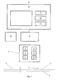
Fig. 1 is a schematic of a scratch detection and analysis apparatus according to one embodiment; and -
Fig. 2 is a flowchart of a scratch detection and analysis method according to another embodiment. - A detailed description of one or more embodiments of the disclosed apparatus and method are presented herein by way of exemplification and not limitation with reference to the Figures. It is to be understood that other embodiments may be utilized and changes may be made without departing from the scope of the present disclosure. In particular, the disclosure provides various examples related to verification of surface defects on aircraft parts, whereas the advantages of the present disclosure as applied in a related field would be apparent to one having ordinary skill in the art and are considered to be within the scope of the present invention.
-
Fig. 1 shows ascratch verification apparatus 1 for verification of defects in asurface 2. Thesurface 2 may comprise acoating 3 disposed on asubstrate 4. Thesurface 2 may comprise one ormore target areas 5 that are analyzed in succession or simultaneously. Thescratch verification apparatus 1 includes adetection device 6 comprising one ormore emission sources 7 and one ormore sensors 8. Theemission sources 7 may be configured to emit a signal over one or more ranges in the electromagnetic spectrum, such as visible light, ultraviolet light, infrared light, etc. Theemission sources 7 may comprise light emitting diodes (LEDs), lasers, or any other sources known in the art. In other examples, one ormore emission sources 7 may be configured to emit sound waves (e.g., ultrasonic), vibration energy, electrical signals, or the like. Theemission sources 7 may be provided in an emission source array. - The signal emitted by the
emission source 7 is emitted onto thesurface 2 and reflected, partially reflected, or at least partially reflected, to the one ormore sensors 8. Thesensors 8 are configured to detect the signal of the one ormore emission sources 7, and may be paired to acorresponding emission source 7. For example, the sensors may be configured to detect electromagnetic radiation from one or more of theemission sources 7 that has been reflected off of thesurface 2. Thesensors 8 configured to detect radiation may be fiber optic sensors, CCD devices, or any other sensor known in the field. In some examples thesensors 8 are configured to detect radiation in specific ranges of the electromagnetic spectrum corresponding to the one ormore emission sources 7. The sensor array may comprisesensors 8 individually configured to detect radiation from a selected range of the electromagnetic spectrum. The selected range of the electromagnetic spectrum may be chosen according to the known properties of thesurface 2 or thecoating 3. In other examples, thesensors 8 may be devices configured to sense sound waves, vibration energy, electrical signals, or any other signal that is emitted by the one ormore emission sources 7. Thesensors 8 may be arranged in a sensor array that comprises a plurality ofsensors 8. In some examples, thedetection device 6 further comprises a resonant chamber for generating a signal that differentiates thecoating 3 from thesubstrate 4. - The
apparatus 1 further comprises aprocessor 9 that receives an input signal from thesensors 8 and processes the input signal, for example, to process an image of thesurface 2 at the location over which theapparatus 1 is scanning. Theprocessor 9 may also be configured to control theemission sources 7; e.g., individually switch thesources 7 on/off, vary the amount of power, etc. Theprocessor 9 may be used to compare the signal emitted by one ormore emission sources 7 with the signal detected by one or more of thecorresponding sensors 8. For example, theprocessor 9 may compare the signals to calculate the phase shift or time shift of a particular signal, to calculate the resistance or other electrical characteristic of the surface between two points, or any other phenomenon that can be used to indicate the properties of the structure. - The
apparatus 1 may further comprise adata source 10 connected to theprocessor 9. In some examples, thedata source 10 may be a locally contained data storage device, such as a flash data storage device, or may be a remote server or other device connected to theprocessor 9 by wireless link or some other communication medium. Information contained on thedata source 10 may be used by theprocessor 9 to analyze and/or classify a particular defect in a surface. Thedata source 10 may also contain information about thesurface 2, such as information specific to the one ormore target areas 5 thereby enabling the apparatus to recognize and differentiate between one ormore target areas 5. Further, each of the one ormore target areas 5 may have a corresponding set of criteria. The set of criteria includes information, such as thresholds or other parameters, that allow theprocessor 9 to determine, for example, whether or not the defect is acceptable or may be repaired. - The
apparatus 1 shown inFig. 1 also includes auser interface 11, which may comprise a display screen for showing images of thesurface 2 or one of thetarget areas 5 of thesurface 2. Theuser interface 11 may also be configured display analysis of a particular defect. Theuser interface 11 may also include one ormore inputs 12, such as buttons, touch screens, etc. Theinputs 12 may allow a user to begin or pause a scan, repeat a scan, compare results, verify thresholds, or any other useful input. In some examples, one of the one ormore inputs 12 allows the user to set the orientation of theapparatus 1 with respect to thesurface 2, allowing the processor to determine the physical location of the boundaries of each of the one ormore target areas 5. In other examples, theprocessor 9 may recognize the boundaries of the one ormore target areas 5 by correlating the particular location with physical features that can be recognized by analyzing the input signal from thedetection device 6. Theuser interface 11 may be directly attached to theprocessor 9 and other features of theapparatus 1, or may comprise another device, such as a computing device in a remote location. - In operation, the
scratch verification apparatus 1 described above is used to verify, i.e., analyze, defects on a surface. In some examples, theapparatus 1 is used to scan a TARGET AREA at a location where a defect is known to exist, i.e., is visible. In other examples, thescratch verification apparatus 1 is used to scan asurface 2 in its entirety to detect and analyze thesurface 2 for a range of defects and provide determinations regarding appropriate corrective measures. Thesurface 2 may be, for example, the outer surface of an entire part, e.g., a rotor for a turbine. Thesurface 2 may comprise a plurality oftarget areas 5, some of which may have acoating 3 while others do not. Further, thecoating 3 may vary from one area of asurface 2 to another. Theapparatus 1 may be configured to recognize where acoating 3 begins relative to where it should begin. Theapparatus 1 may also be configured to vary the signal emitted from theemission sources 7 according to the material forming thesubstrate 4 and thecoating 3. - A method of detecting and/or analyzing a surface defect is shown in
Fig. 2 . First, the apparatus is aligned with the surface. By aligning, it is meant that the apparatus achieves an orientation with the surface from which a scan may commence that allows the apparatus to identify boundaries of the surface and associated areas of the surface, which may correlate to different sets of criteria for analyzing defects. This may be accomplished by bringing the apparatus into a first location where the orientation of the apparatus to the surface is known. This location may then be verified by the detection device of the apparatus. In other examples, the step of aligning the apparatus with the surface may be accomplished by placing the apparatus in a scanning position with respect to a selected target area or portion thereof where a defect has been identified or may exist. In some examples, the step of aligning the part with the surface may further comprise identifying the surface and/or the target area where the scan is to begin, such as by user input. - The surface is then scanned with the detection device of the apparatus. As noted above, the emission sources and/or the sensors of the detection device may be controlled to operate in a manner specific to a particular coating, substrate, or other attribute, including according to defects of interest for a particular target area. For example, in some locations a scratch in the coating may be acceptable where as an omission of the coating in that area may not. Also, in some locations a scratch in the coating may be analyzed and determined that corrective action is acceptable, where a scratch in the substrate with the coating applied on the top thereof would otherwise render the surface unacceptable, resulting in a determination that the surface should be discarded.
- The information received from the detection device is then processed, for example, according to the arrangement of the detection device. The processed information may include a first data set representing information from a first range of the electromagnetic spectrum and a second data set representing information from a second range of the electromagnetic spectrum. The processed information may be further divided into a plurality of data sets based on electromagnetic spectrum, angle with respect to the surface, etc. The processed information can then be analyzed by comparing the processed information to a set of criteria for a selected target area to determine the presence of any defects, whether or not those defects may be corrected, and whether or not the surface (part) should be discarded. This determination can then be returned to the user or to another device. In some examples, the steps recited above may be repeated for each of a plurality of target areas on a surface.
- While the invention has been described with reference to an exemplary embodiment or embodiments, it will be understood by those skilled in the art that various changes may be made and equivalents may be substituted for elements thereof without departing from the scope of the invention. In addition, many modifications may be made to adapt a particular situation or material to the teachings of the invention without departing from the essential scope thereof. Also, in the drawings and the description, there have been disclosed exemplary embodiments of the invention and, although specific terms may have been employed, they are unless otherwise stated used in a generic and descriptive sense only and not for purposes of limitation, the scope of the invention therefore not being so limited. Moreover, the use of the terms first, second, etc. , do not denote any order or importance, but rather the terms first, second, etc. are used to distinguish one element from another. Furthermore, the use of the terms a, an, etc. do not denote a limitation of quantity, but rather denote the presence of at least one of the referenced item.
Claims (8)
- A method of verifying defects in a surface (2), comprising:aligning a verification apparatus (1) with respect to a first target area (5) of a surface;scanning a first target area (5) of a surface (2) with a detection device (6) having one or emission sources (7) and one or more sensors (8);processing information generated by the detection device (6) with a processor (9) to generate one or more data sets describing the first target area (5);comparing the one or more data sets describing the first target area (5) with a first set of criteria associated with the first target area (5) to determine an appropriate action.
- The method of claim 1, further comprising:recognizing a boundary between the first target area (5) and a second target area (5);scanning the second target area (5) of the surface (2) with the detection device (6);processing information generated by the detection device (6) with a processor (9) to generate one or more data sets describing the second target area (5); andcomparing the one or more data sets describing the second target area (5) with a second set of criteria associated with the second target area (5) to determine an appropriate action.
- The method of claim 1 or 2, wherein the one or more emission sources (7) include a first emission source (7) emitting energy from a first portion of the electromagnetic spectrum and a second emission source (7) emitting energy from a second portion of the electromagnetic spectrum.
- The method of claim 3, wherein the one or more data sets include a first data set representing data from the first portion of the electromagnetic spectrum and a second data set representing data from the second portion of the electromagnetic spectrum.
- A scratch verification apparatus (1) for detecting and analyzing defects in a surface, comprising:a detection device (6) having a plurality of emission sources (7) and a plurality of sensors (8), wherein the emission sources (7) include a first emission source (7) emitting a first signal and a second emission source (7) a second signal that differs from the first signal;a processor (9) connected to the detection device (8), the processor (9) configured to apply one or more sets of criteria to one or more corresponding target areas (5) of a surface (2), the processor (9) configured to differentiate between data from the one or more target areas (5); anda data source (10) connected to the processor (9), the data source (10) containing information regarding one or more boundaries of the one or more target areas (5), the data source (10) further containing the one or more sets of criteria.
- The scratch verification device of claim 5, further comprising a user interface (11).
- The scratch verification device of claim 5 or 6, wherein the data source (10) further comprises a remote server or a flash data storage device.
- The scratch verification device of claim 5, 6 or 7, wherein the detection device (6) further comprises a resonant chamber.
Applications Claiming Priority (1)
| Application Number | Priority Date | Filing Date | Title |
|---|---|---|---|
| US14/297,699 US20150355099A1 (en) | 2014-06-06 | 2014-06-06 | Scratch verification apparatus and method |
Publications (1)
| Publication Number | Publication Date |
|---|---|
| EP2952889A1 true EP2952889A1 (en) | 2015-12-09 |
Family
ID=53373306
Family Applications (1)
| Application Number | Title | Priority Date | Filing Date |
|---|---|---|---|
| EP15170778.3A Withdrawn EP2952889A1 (en) | 2014-06-06 | 2015-06-05 | Scratch verification apparatus and method |
Country Status (2)
| Country | Link |
|---|---|
| US (1) | US20150355099A1 (en) |
| EP (1) | EP2952889A1 (en) |
Citations (11)
| Publication number | Priority date | Publication date | Assignee | Title |
|---|---|---|---|---|
| WO1987000629A1 (en) * | 1985-07-15 | 1987-01-29 | Sira Limited | Inspection apparatus |
| US5389794A (en) * | 1992-11-25 | 1995-02-14 | Qc Optics, Inc. | Surface pit and mound detection and discrimination system and method |
| US6198529B1 (en) * | 1999-04-30 | 2001-03-06 | International Business Machines Corporation | Automated inspection system for metallic surfaces |
| US20020118892A1 (en) * | 1997-07-07 | 2002-08-29 | Van-Duc Nguyen | Method and apparatus for image registration |
| US20030030002A1 (en) * | 2000-06-05 | 2003-02-13 | Morteza Safai | Infrared crack detection apparatus and method |
| US20040119018A1 (en) * | 2002-08-31 | 2004-06-24 | Alfano Robert R. | Systems and methods for non-destructively detecting material abnormalities beneath a coated surface |
| US20060043303A1 (en) * | 2003-07-16 | 2006-03-02 | The Boeing Company | Non-destructive infrared inspection device |
| US20060082590A1 (en) * | 2004-10-14 | 2006-04-20 | Stevick Glen R | Method and apparatus for dynamic space-time imaging system |
| EP1890134A2 (en) * | 2006-08-17 | 2008-02-20 | Massen Machine Vision Systems GmbH | Quality surveillance of patterned, in particular spatially curvilinear surfaces |
| US20080111074A1 (en) * | 2004-10-22 | 2008-05-15 | Northrop Grumman Corporation | Method for infrared imaging of substrates through coatings |
| WO2008080602A1 (en) * | 2006-12-29 | 2008-07-10 | Isam Aktiengesellschaft | Method for analyzing the surface of a work piece, especially of a lay of fibers and/or woven fibers |
Family Cites Families (12)
| Publication number | Priority date | Publication date | Assignee | Title |
|---|---|---|---|---|
| US4920385A (en) * | 1984-02-14 | 1990-04-24 | Diffracto Ltd. | Panel surface flaw inspection |
| US5127726A (en) * | 1989-05-19 | 1992-07-07 | Eastman Kodak Company | Method and apparatus for low angle, high resolution surface inspection |
| US5440127A (en) * | 1993-05-17 | 1995-08-08 | Simco/Ramic Corporation | Method and apparatus for illuminating target specimens in inspection systems |
| US6956644B2 (en) * | 1997-09-19 | 2005-10-18 | Kla-Tencor Technologies Corporation | Systems and methods for a wafer inspection system using multiple angles and multiple wavelength illumination |
| US6201601B1 (en) * | 1997-09-19 | 2001-03-13 | Kla-Tencor Corporation | Sample inspection system |
| US7433031B2 (en) * | 2003-10-29 | 2008-10-07 | Core Tech Optical, Inc. | Defect review system with 2D scanning and a ring detector |
| US7110106B2 (en) * | 2003-10-29 | 2006-09-19 | Coretech Optical, Inc. | Surface inspection system |
| US7249512B2 (en) * | 2005-01-24 | 2007-07-31 | The Boeing Company | Non-destructive stringer inspection apparatus and method |
| US7879276B2 (en) * | 2007-11-08 | 2011-02-01 | The Boeing Company | Foam stiffened hollow composite stringer |
| CN103221804A (en) * | 2010-09-10 | 2013-07-24 | 集成电子制造公司 | Signal and detection system for keying applications |
| US20140085458A1 (en) * | 2012-09-26 | 2014-03-27 | Apple Inc. | Angular visual response of cosmetic surfaces |
| US9606070B2 (en) * | 2014-11-25 | 2017-03-28 | The Boeing Company | Multispectral imaging system and method for detecting foreign object debris |
-
2014
- 2014-06-06 US US14/297,699 patent/US20150355099A1/en not_active Abandoned
-
2015
- 2015-06-05 EP EP15170778.3A patent/EP2952889A1/en not_active Withdrawn
Patent Citations (11)
| Publication number | Priority date | Publication date | Assignee | Title |
|---|---|---|---|---|
| WO1987000629A1 (en) * | 1985-07-15 | 1987-01-29 | Sira Limited | Inspection apparatus |
| US5389794A (en) * | 1992-11-25 | 1995-02-14 | Qc Optics, Inc. | Surface pit and mound detection and discrimination system and method |
| US20020118892A1 (en) * | 1997-07-07 | 2002-08-29 | Van-Duc Nguyen | Method and apparatus for image registration |
| US6198529B1 (en) * | 1999-04-30 | 2001-03-06 | International Business Machines Corporation | Automated inspection system for metallic surfaces |
| US20030030002A1 (en) * | 2000-06-05 | 2003-02-13 | Morteza Safai | Infrared crack detection apparatus and method |
| US20040119018A1 (en) * | 2002-08-31 | 2004-06-24 | Alfano Robert R. | Systems and methods for non-destructively detecting material abnormalities beneath a coated surface |
| US20060043303A1 (en) * | 2003-07-16 | 2006-03-02 | The Boeing Company | Non-destructive infrared inspection device |
| US20060082590A1 (en) * | 2004-10-14 | 2006-04-20 | Stevick Glen R | Method and apparatus for dynamic space-time imaging system |
| US20080111074A1 (en) * | 2004-10-22 | 2008-05-15 | Northrop Grumman Corporation | Method for infrared imaging of substrates through coatings |
| EP1890134A2 (en) * | 2006-08-17 | 2008-02-20 | Massen Machine Vision Systems GmbH | Quality surveillance of patterned, in particular spatially curvilinear surfaces |
| WO2008080602A1 (en) * | 2006-12-29 | 2008-07-10 | Isam Aktiengesellschaft | Method for analyzing the surface of a work piece, especially of a lay of fibers and/or woven fibers |
Also Published As
| Publication number | Publication date |
|---|---|
| US20150355099A1 (en) | 2015-12-10 |
Similar Documents
| Publication | Publication Date | Title |
|---|---|---|
| US11029255B2 (en) | Defect inspection device, defect inspection method, and program | |
| JP2015172576A5 (en) | Method and system for inspection of complex item | |
| US20200096454A1 (en) | Defect detection system for aircraft component and defect detection method for aircraft component | |
| CN112534470A (en) | System and method for image-based inspection of target objects | |
| JP6283534B2 (en) | Tire deterioration evaluation apparatus and system, method and program thereof | |
| JP2017083312A (en) | Surface damage detection method and surface damage detection device | |
| CN104103224B (en) | Panel inspection method and equipment | |
| CN108780033B (en) | Method for controlling probe, detection equipment and device for controlling probe | |
| KR101308098B1 (en) | Multi-touch point detection method of infrared rays multi-touch screen | |
| WO2019238152A3 (en) | Inspection method and system | |
| EP2952889A1 (en) | Scratch verification apparatus and method | |
| EP3671205B1 (en) | Laser ultrasound imaging for determining structural characteristics | |
| CN104655653A (en) | Method and apparatus for inspecting printed circuit board | |
| CN109884078B (en) | Layered wafer inspection | |
| KR20190054698A (en) | Structural health monitoring system using visible camera and thermo-graphic camera | |
| CN105373788A (en) | Light deflection detection module and measurement and calibration method using the same | |
| JP5480424B1 (en) | Defect location analysis system and method | |
| US10775330B2 (en) | Thermo-chromatic witness features for lightning strike indication in both metallic and composite structures | |
| JP2015155831A (en) | Package inspection apparatus | |
| JP6829778B2 (en) | Object identification device and object identification method | |
| KR101127796B1 (en) | An Glass Substrate Crack Montoring Method and Unit | |
| KR20170075101A (en) | Apparatus and method for steel sheet inspection | |
| JP2006226834A (en) | Surface inspection device and surface inspection method | |
| CN112912931A (en) | Auto-calibration of multiple cameras using near infrared illuminators | |
| KR102073243B1 (en) | Examining apparatus and method for triplex bonding layer |
Legal Events
| Date | Code | Title | Description |
|---|---|---|---|
| PUAI | Public reference made under article 153(3) epc to a published international application that has entered the european phase |
Free format text: ORIGINAL CODE: 0009012 |
|
| AK | Designated contracting states |
Kind code of ref document: A1 Designated state(s): AL AT BE BG CH CY CZ DE DK EE ES FI FR GB GR HR HU IE IS IT LI LT LU LV MC MK MT NL NO PL PT RO RS SE SI SK SM TR |
|
| AX | Request for extension of the european patent |
Extension state: BA ME |
|
| 17P | Request for examination filed |
Effective date: 20160608 |
|
| RBV | Designated contracting states (corrected) |
Designated state(s): AL AT BE BG CH CY CZ DE DK EE ES FI FR GB GR HR HU IE IS IT LI LT LU LV MC MK MT NL NO PL PT RO RS SE SI SK SM TR |
|
| 17Q | First examination report despatched |
Effective date: 20180814 |
|
| STAA | Information on the status of an ep patent application or granted ep patent |
Free format text: STATUS: THE APPLICATION HAS BEEN WITHDRAWN |
|
| 18W | Application withdrawn |
Effective date: 20190107 |