EP2927294B1 - Polishing compositions and methods for selectively polishing silicon nitride over silicon oxide films - Google Patents
Polishing compositions and methods for selectively polishing silicon nitride over silicon oxide films Download PDFInfo
- Publication number
- EP2927294B1 EP2927294B1 EP15158633.6A EP15158633A EP2927294B1 EP 2927294 B1 EP2927294 B1 EP 2927294B1 EP 15158633 A EP15158633 A EP 15158633A EP 2927294 B1 EP2927294 B1 EP 2927294B1
- Authority
- EP
- European Patent Office
- Prior art keywords
- acid
- anionic
- polishing
- composition
- polishing composition
- Prior art date
- Legal status (The legal status is an assumption and is not a legal conclusion. Google has not performed a legal analysis and makes no representation as to the accuracy of the status listed.)
- Active
Links
- 239000000203 mixture Substances 0.000 title claims description 177
- 238000005498 polishing Methods 0.000 title claims description 134
- 229910052581 Si3N4 Inorganic materials 0.000 title claims description 103
- HQVNEWCFYHHQES-UHFFFAOYSA-N silicon nitride Chemical compound N12[Si]34N5[Si]62N3[Si]51N64 HQVNEWCFYHHQES-UHFFFAOYSA-N 0.000 title claims description 103
- VYPSYNLAJGMNEJ-UHFFFAOYSA-N Silicium dioxide Chemical compound O=[Si]=O VYPSYNLAJGMNEJ-UHFFFAOYSA-N 0.000 title claims description 91
- 229910052814 silicon oxide Inorganic materials 0.000 title claims description 46
- 238000000034 method Methods 0.000 title claims description 33
- 125000000129 anionic group Chemical group 0.000 claims description 68
- 239000003623 enhancer Substances 0.000 claims description 30
- 150000004767 nitrides Chemical class 0.000 claims description 29
- 239000002245 particle Substances 0.000 claims description 21
- 239000000377 silicon dioxide Substances 0.000 claims description 21
- 239000000758 substrate Substances 0.000 claims description 21
- 230000001965 increasing effect Effects 0.000 claims description 14
- 229920006318 anionic polymer Polymers 0.000 claims description 13
- 239000003945 anionic surfactant Substances 0.000 claims description 13
- XLYOFNOQVPJJNP-UHFFFAOYSA-N water Substances O XLYOFNOQVPJJNP-UHFFFAOYSA-N 0.000 claims description 13
- QTBSBXVTEAMEQO-UHFFFAOYSA-N Acetic acid Chemical compound CC(O)=O QTBSBXVTEAMEQO-UHFFFAOYSA-N 0.000 claims description 12
- KWYUFKZDYYNOTN-UHFFFAOYSA-M Potassium hydroxide Chemical compound [OH-].[K+] KWYUFKZDYYNOTN-UHFFFAOYSA-M 0.000 claims description 12
- 239000002253 acid Substances 0.000 claims description 12
- 125000003178 carboxy group Chemical group [H]OC(*)=O 0.000 claims description 11
- -1 alkylbenzene sulfonate Chemical class 0.000 claims description 10
- 150000007942 carboxylates Chemical group 0.000 claims description 10
- 239000004065 semiconductor Substances 0.000 claims description 10
- OFOBLEOULBTSOW-UHFFFAOYSA-N Malonic acid Chemical compound OC(=O)CC(O)=O OFOBLEOULBTSOW-UHFFFAOYSA-N 0.000 claims description 8
- XBDQKXXYIPTUBI-UHFFFAOYSA-N dimethylselenoniopropionate Natural products CCC(O)=O XBDQKXXYIPTUBI-UHFFFAOYSA-N 0.000 claims description 8
- 239000012141 concentrate Substances 0.000 claims description 7
- 238000004519 manufacturing process Methods 0.000 claims description 7
- 229910021420 polycrystalline silicon Inorganic materials 0.000 claims description 7
- HEMHJVSKTPXQMS-UHFFFAOYSA-M Sodium hydroxide Chemical compound [OH-].[Na+] HEMHJVSKTPXQMS-UHFFFAOYSA-M 0.000 claims description 6
- GWEVSGVZZGPLCZ-UHFFFAOYSA-N Titan oxide Chemical compound O=[Ti]=O GWEVSGVZZGPLCZ-UHFFFAOYSA-N 0.000 claims description 6
- MCMNRKCIXSYSNV-UHFFFAOYSA-N Zirconium dioxide Chemical compound O=[Zr]=O MCMNRKCIXSYSNV-UHFFFAOYSA-N 0.000 claims description 6
- PNEYBMLMFCGWSK-UHFFFAOYSA-N aluminium oxide Inorganic materials [O-2].[O-2].[O-2].[Al+3].[Al+3] PNEYBMLMFCGWSK-UHFFFAOYSA-N 0.000 claims description 6
- KRKNYBCHXYNGOX-UHFFFAOYSA-N citric acid Chemical compound OC(=O)CC(O)(C(O)=O)CC(O)=O KRKNYBCHXYNGOX-UHFFFAOYSA-N 0.000 claims description 6
- JVTAAEKCZFNVCJ-UHFFFAOYSA-N lactic acid Chemical compound CC(O)C(O)=O JVTAAEKCZFNVCJ-UHFFFAOYSA-N 0.000 claims description 6
- 150000001732 carboxylic acid derivatives Chemical class 0.000 claims description 5
- 229920005591 polysilicon Polymers 0.000 claims description 5
- DHMQDGOQFOQNFH-UHFFFAOYSA-N Glycine Chemical compound NCC(O)=O DHMQDGOQFOQNFH-UHFFFAOYSA-N 0.000 claims description 4
- SEQKRHFRPICQDD-UHFFFAOYSA-N N-tris(hydroxymethyl)methylglycine Chemical compound OCC(CO)(CO)[NH2+]CC([O-])=O SEQKRHFRPICQDD-UHFFFAOYSA-N 0.000 claims description 4
- 229910019142 PO4 Inorganic materials 0.000 claims description 4
- 235000011054 acetic acid Nutrition 0.000 claims description 4
- WPYMKLBDIGXBTP-UHFFFAOYSA-N benzoic acid Chemical compound OC(=O)C1=CC=CC=C1 WPYMKLBDIGXBTP-UHFFFAOYSA-N 0.000 claims description 4
- CETPSERCERDGAM-UHFFFAOYSA-N ceric oxide Chemical compound O=[Ce]=O CETPSERCERDGAM-UHFFFAOYSA-N 0.000 claims description 4
- 229910000422 cerium(IV) oxide Inorganic materials 0.000 claims description 4
- 239000008119 colloidal silica Substances 0.000 claims description 4
- 230000006866 deterioration Effects 0.000 claims description 4
- BDAGIHXWWSANSR-UHFFFAOYSA-N methanoic acid Natural products OC=O BDAGIHXWWSANSR-UHFFFAOYSA-N 0.000 claims description 4
- LCPDWSOZIOUXRV-UHFFFAOYSA-N phenoxyacetic acid Chemical compound OC(=O)COC1=CC=CC=C1 LCPDWSOZIOUXRV-UHFFFAOYSA-N 0.000 claims description 4
- SCVFZCLFOSHCOH-UHFFFAOYSA-M potassium acetate Chemical compound [K+].CC([O-])=O SCVFZCLFOSHCOH-UHFFFAOYSA-M 0.000 claims description 4
- 235000019260 propionic acid Nutrition 0.000 claims description 4
- IUVKMZGDUIUOCP-BTNSXGMBSA-N quinbolone Chemical compound O([C@H]1CC[C@H]2[C@H]3[C@@H]([C@]4(C=CC(=O)C=C4CC3)C)CC[C@@]21C)C1=CCCC1 IUVKMZGDUIUOCP-BTNSXGMBSA-N 0.000 claims description 4
- VDZOOKBUILJEDG-UHFFFAOYSA-M tetrabutylammonium hydroxide Chemical compound [OH-].CCCC[N+](CCCC)(CCCC)CCCC VDZOOKBUILJEDG-UHFFFAOYSA-M 0.000 claims description 4
- WGTYBPLFGIVFAS-UHFFFAOYSA-M tetramethylammonium hydroxide Chemical compound [OH-].C[N+](C)(C)C WGTYBPLFGIVFAS-UHFFFAOYSA-M 0.000 claims description 4
- 239000004310 lactic acid Substances 0.000 claims description 3
- 235000014655 lactic acid Nutrition 0.000 claims description 3
- NBIIXXVUZAFLBC-UHFFFAOYSA-K phosphate Chemical compound [O-]P([O-])([O-])=O NBIIXXVUZAFLBC-UHFFFAOYSA-K 0.000 claims description 3
- 239000010452 phosphate Substances 0.000 claims description 3
- BDHFUVZGWQCTTF-UHFFFAOYSA-M sulfonate Chemical compound [O-]S(=O)=O BDHFUVZGWQCTTF-UHFFFAOYSA-M 0.000 claims description 3
- BJEPYKJPYRNKOW-REOHCLBHSA-N (S)-malic acid Chemical compound OC(=O)[C@@H](O)CC(O)=O BJEPYKJPYRNKOW-REOHCLBHSA-N 0.000 claims description 2
- RBNPOMFGQQGHHO-UHFFFAOYSA-N -2,3-Dihydroxypropanoic acid Natural products OCC(O)C(O)=O RBNPOMFGQQGHHO-UHFFFAOYSA-N 0.000 claims description 2
- MFGOFGRYDNHJTA-UHFFFAOYSA-N 2-amino-1-(2-fluorophenyl)ethanol Chemical compound NCC(O)C1=CC=CC=C1F MFGOFGRYDNHJTA-UHFFFAOYSA-N 0.000 claims description 2
- OSWFIVFLDKOXQC-UHFFFAOYSA-N 4-(3-methoxyphenyl)aniline Chemical compound COC1=CC=CC(C=2C=CC(N)=CC=2)=C1 OSWFIVFLDKOXQC-UHFFFAOYSA-N 0.000 claims description 2
- VHUUQVKOLVNVRT-UHFFFAOYSA-N Ammonium hydroxide Chemical compound [NH4+].[OH-] VHUUQVKOLVNVRT-UHFFFAOYSA-N 0.000 claims description 2
- 239000005711 Benzoic acid Substances 0.000 claims description 2
- LSNNMFCWUKXFEE-UHFFFAOYSA-M Bisulfite Chemical compound OS([O-])=O LSNNMFCWUKXFEE-UHFFFAOYSA-M 0.000 claims description 2
- RBNPOMFGQQGHHO-UWTATZPHSA-N D-glyceric acid Chemical compound OC[C@@H](O)C(O)=O RBNPOMFGQQGHHO-UWTATZPHSA-N 0.000 claims description 2
- QEVGZEDELICMKH-UHFFFAOYSA-N Diglycolic acid Chemical compound OC(=O)COCC(O)=O QEVGZEDELICMKH-UHFFFAOYSA-N 0.000 claims description 2
- KDYFGRWQOYBRFD-UHFFFAOYSA-N Succinic acid Natural products OC(=O)CCC(O)=O KDYFGRWQOYBRFD-UHFFFAOYSA-N 0.000 claims description 2
- UZMAPBJVXOGOFT-UHFFFAOYSA-N Syringetin Natural products COC1=C(O)C(OC)=CC(C2=C(C(=O)C3=C(O)C=C(O)C=C3O2)O)=C1 UZMAPBJVXOGOFT-UHFFFAOYSA-N 0.000 claims description 2
- 239000007997 Tricine buffer Substances 0.000 claims description 2
- BJEPYKJPYRNKOW-UHFFFAOYSA-N alpha-hydroxysuccinic acid Natural products OC(=O)C(O)CC(O)=O BJEPYKJPYRNKOW-UHFFFAOYSA-N 0.000 claims description 2
- 239000000908 ammonium hydroxide Substances 0.000 claims description 2
- 235000010233 benzoic acid Nutrition 0.000 claims description 2
- KDYFGRWQOYBRFD-NUQCWPJISA-N butanedioic acid Chemical compound O[14C](=O)CC[14C](O)=O KDYFGRWQOYBRFD-NUQCWPJISA-N 0.000 claims description 2
- HUCVOHYBFXVBRW-UHFFFAOYSA-M caesium hydroxide Inorganic materials [OH-].[Cs+] HUCVOHYBFXVBRW-UHFFFAOYSA-M 0.000 claims description 2
- 235000015165 citric acid Nutrition 0.000 claims description 2
- KCFYHBSOLOXZIF-UHFFFAOYSA-N dihydrochrysin Natural products COC1=C(O)C(OC)=CC(C2OC3=CC(O)=CC(O)=C3C(=O)C2)=C1 KCFYHBSOLOXZIF-UHFFFAOYSA-N 0.000 claims description 2
- 235000019253 formic acid Nutrition 0.000 claims description 2
- 229960002449 glycine Drugs 0.000 claims description 2
- 235000013905 glycine and its sodium salt Nutrition 0.000 claims description 2
- 239000001630 malic acid Substances 0.000 claims description 2
- 235000011090 malic acid Nutrition 0.000 claims description 2
- 235000011056 potassium acetate Nutrition 0.000 claims description 2
- 229960004109 potassium acetate Drugs 0.000 claims description 2
- 239000001508 potassium citrate Substances 0.000 claims description 2
- 229960002635 potassium citrate Drugs 0.000 claims description 2
- QEEAPRPFLLJWCF-UHFFFAOYSA-K potassium citrate (anhydrous) Chemical compound [K+].[K+].[K+].[O-]C(=O)CC(O)(CC([O-])=O)C([O-])=O QEEAPRPFLLJWCF-UHFFFAOYSA-K 0.000 claims description 2
- 235000011082 potassium citrates Nutrition 0.000 claims description 2
- UJJLJRQIPMGXEZ-UHFFFAOYSA-N tetrahydro-2-furoic acid Chemical compound OC(=O)C1CCCO1 UJJLJRQIPMGXEZ-UHFFFAOYSA-N 0.000 claims description 2
- MUBZPKHOEPUJKR-UHFFFAOYSA-N Oxalic acid Chemical compound OC(=O)C(O)=O MUBZPKHOEPUJKR-UHFFFAOYSA-N 0.000 claims 3
- RGHNJXZEOKUKBD-SQOUGZDYSA-N D-gluconic acid Chemical group OC[C@@H](O)[C@@H](O)[C@H](O)[C@@H](O)C(O)=O RGHNJXZEOKUKBD-SQOUGZDYSA-N 0.000 claims 2
- AEMRFAOFKBGASW-UHFFFAOYSA-N Glycolic acid Chemical compound OCC(O)=O AEMRFAOFKBGASW-UHFFFAOYSA-N 0.000 claims 2
- KFSLWBXXFJQRDL-UHFFFAOYSA-N Peracetic acid Chemical compound CC(=O)OO KFSLWBXXFJQRDL-UHFFFAOYSA-N 0.000 claims 2
- RGHNJXZEOKUKBD-UHFFFAOYSA-N D-gluconic acid Natural products OCC(O)C(O)C(O)C(O)C(O)=O RGHNJXZEOKUKBD-UHFFFAOYSA-N 0.000 claims 1
- FEWJPZIEWOKRBE-JCYAYHJZSA-N Dextrotartaric acid Chemical compound OC(=O)[C@H](O)[C@@H](O)C(O)=O FEWJPZIEWOKRBE-JCYAYHJZSA-N 0.000 claims 1
- HNDVDQJCIGZPNO-YFKPBYRVSA-N L-histidine Chemical compound OC(=O)[C@@H](N)CC1=CN=CN1 HNDVDQJCIGZPNO-YFKPBYRVSA-N 0.000 claims 1
- OUYCCCASQSFEME-QMMMGPOBSA-N L-tyrosine Chemical compound OC(=O)[C@@H](N)CC1=CC=C(O)C=C1 OUYCCCASQSFEME-QMMMGPOBSA-N 0.000 claims 1
- FEWJPZIEWOKRBE-UHFFFAOYSA-N Tartaric acid Natural products [H+].[H+].[O-]C(=O)C(O)C(O)C([O-])=O FEWJPZIEWOKRBE-UHFFFAOYSA-N 0.000 claims 1
- 150000004996 alkyl benzenes Chemical class 0.000 claims 1
- 150000008051 alkyl sulfates Chemical class 0.000 claims 1
- 239000000174 gluconic acid Substances 0.000 claims 1
- 235000012208 gluconic acid Nutrition 0.000 claims 1
- HNDVDQJCIGZPNO-UHFFFAOYSA-N histidine Natural products OC(=O)C(N)CC1=CN=CN1 HNDVDQJCIGZPNO-UHFFFAOYSA-N 0.000 claims 1
- 150000002430 hydrocarbons Chemical group 0.000 claims 1
- 229960000448 lactic acid Drugs 0.000 claims 1
- 235000006408 oxalic acid Nutrition 0.000 claims 1
- 125000002467 phosphate group Chemical group [H]OP(=O)(O[H])O[*] 0.000 claims 1
- 239000011975 tartaric acid Substances 0.000 claims 1
- 235000002906 tartaric acid Nutrition 0.000 claims 1
- OUYCCCASQSFEME-UHFFFAOYSA-N tyrosine Natural products OC(=O)C(N)CC1=CC=C(O)C=C1 OUYCCCASQSFEME-UHFFFAOYSA-N 0.000 claims 1
- 235000012431 wafers Nutrition 0.000 description 24
- 239000002002 slurry Substances 0.000 description 23
- 239000003082 abrasive agent Substances 0.000 description 19
- 239000000463 material Substances 0.000 description 17
- 239000010410 layer Substances 0.000 description 15
- 230000008569 process Effects 0.000 description 11
- 239000000126 substance Substances 0.000 description 9
- 230000002378 acidificating effect Effects 0.000 description 7
- 229910052751 metal Inorganic materials 0.000 description 7
- 239000002184 metal Substances 0.000 description 7
- 239000000523 sample Substances 0.000 description 7
- 230000010354 integration Effects 0.000 description 6
- 239000000654 additive Substances 0.000 description 5
- 230000008901 benefit Effects 0.000 description 5
- 238000001246 colloidal dispersion Methods 0.000 description 5
- 238000005516 engineering process Methods 0.000 description 5
- 230000002195 synergetic effect Effects 0.000 description 5
- NBIIXXVUZAFLBC-UHFFFAOYSA-N Phosphoric acid Chemical compound OP(O)(O)=O NBIIXXVUZAFLBC-UHFFFAOYSA-N 0.000 description 4
- 229910052802 copper Inorganic materials 0.000 description 4
- 239000010949 copper Substances 0.000 description 4
- 239000003989 dielectric material Substances 0.000 description 4
- 239000006185 dispersion Substances 0.000 description 4
- 230000004044 response Effects 0.000 description 4
- 239000004094 surface-active agent Substances 0.000 description 4
- 150000007513 acids Chemical class 0.000 description 3
- 230000000996 additive effect Effects 0.000 description 3
- 125000002091 cationic group Chemical group 0.000 description 3
- 238000002296 dynamic light scattering Methods 0.000 description 3
- 238000009472 formulation Methods 0.000 description 3
- 150000002739 metals Chemical class 0.000 description 3
- 230000004048 modification Effects 0.000 description 3
- 238000012986 modification Methods 0.000 description 3
- 230000009467 reduction Effects 0.000 description 3
- GPRLSGONYQIRFK-MNYXATJNSA-N triton Chemical compound [3H+] GPRLSGONYQIRFK-MNYXATJNSA-N 0.000 description 3
- RYGMFSIKBFXOCR-UHFFFAOYSA-N Copper Chemical compound [Cu] RYGMFSIKBFXOCR-UHFFFAOYSA-N 0.000 description 2
- GRYLNZFGIOXLOG-UHFFFAOYSA-N Nitric acid Chemical compound O[N+]([O-])=O GRYLNZFGIOXLOG-UHFFFAOYSA-N 0.000 description 2
- QAOWNCQODCNURD-UHFFFAOYSA-L Sulfate Chemical compound [O-]S([O-])(=O)=O QAOWNCQODCNURD-UHFFFAOYSA-L 0.000 description 2
- 239000006061 abrasive grain Substances 0.000 description 2
- WNLRTRBMVRJNCN-UHFFFAOYSA-N adipic acid Chemical compound OC(=O)CCCCC(O)=O WNLRTRBMVRJNCN-UHFFFAOYSA-N 0.000 description 2
- 229910000147 aluminium phosphate Inorganic materials 0.000 description 2
- 230000004888 barrier function Effects 0.000 description 2
- 230000009286 beneficial effect Effects 0.000 description 2
- 150000001735 carboxylic acids Chemical class 0.000 description 2
- 150000001875 compounds Chemical class 0.000 description 2
- 230000007423 decrease Effects 0.000 description 2
- 238000010790 dilution Methods 0.000 description 2
- 239000012895 dilution Substances 0.000 description 2
- 230000000694 effects Effects 0.000 description 2
- 238000005530 etching Methods 0.000 description 2
- 230000003993 interaction Effects 0.000 description 2
- 239000007788 liquid Substances 0.000 description 2
- 229910017604 nitric acid Inorganic materials 0.000 description 2
- 238000002161 passivation Methods 0.000 description 2
- 238000001179 sorption measurement Methods 0.000 description 2
- 229910052715 tantalum Inorganic materials 0.000 description 2
- 229910052721 tungsten Inorganic materials 0.000 description 2
- 229910052720 vanadium Inorganic materials 0.000 description 2
- FKKAGFLIPSSCHT-UHFFFAOYSA-N 1-dodecoxydodecane;sulfuric acid Chemical compound OS(O)(=O)=O.CCCCCCCCCCCCOCCCCCCCCCCCC FKKAGFLIPSSCHT-UHFFFAOYSA-N 0.000 description 1
- DBVJJBKOTRCVKF-UHFFFAOYSA-N Etidronic acid Chemical compound OP(=O)(O)C(O)(C)P(O)(O)=O DBVJJBKOTRCVKF-UHFFFAOYSA-N 0.000 description 1
- 241001481828 Glyptocephalus cynoglossus Species 0.000 description 1
- 229910004012 SiCx Inorganic materials 0.000 description 1
- QAOWNCQODCNURD-UHFFFAOYSA-N Sulfuric acid Chemical compound OS(O)(=O)=O QAOWNCQODCNURD-UHFFFAOYSA-N 0.000 description 1
- 229920013812 TRITON H-55 Polymers 0.000 description 1
- 229920013813 TRITON H-66 Polymers 0.000 description 1
- 239000001361 adipic acid Substances 0.000 description 1
- 235000011037 adipic acid Nutrition 0.000 description 1
- 230000015572 biosynthetic process Effects 0.000 description 1
- 230000008859 change Effects 0.000 description 1
- 238000007385 chemical modification Methods 0.000 description 1
- 239000003795 chemical substances by application Substances 0.000 description 1
- 230000015271 coagulation Effects 0.000 description 1
- 238000005345 coagulation Methods 0.000 description 1
- 229910017052 cobalt Inorganic materials 0.000 description 1
- 239000010941 cobalt Substances 0.000 description 1
- GUTLYIVDDKVIGB-UHFFFAOYSA-N cobalt atom Chemical compound [Co] GUTLYIVDDKVIGB-UHFFFAOYSA-N 0.000 description 1
- 239000000084 colloidal system Substances 0.000 description 1
- 239000013068 control sample Substances 0.000 description 1
- 230000003247 decreasing effect Effects 0.000 description 1
- 230000001419 dependent effect Effects 0.000 description 1
- 238000010586 diagram Methods 0.000 description 1
- 239000010432 diamond Substances 0.000 description 1
- 238000009792 diffusion process Methods 0.000 description 1
- 238000007865 diluting Methods 0.000 description 1
- 239000002612 dispersion medium Substances 0.000 description 1
- 230000002708 enhancing effect Effects 0.000 description 1
- 239000012530 fluid Substances 0.000 description 1
- 230000006870 function Effects 0.000 description 1
- 125000001183 hydrocarbyl group Chemical group 0.000 description 1
- 150000002500 ions Chemical class 0.000 description 1
- 238000002955 isolation Methods 0.000 description 1
- 230000007774 longterm Effects 0.000 description 1
- 208000005340 mucopolysaccharidosis III Diseases 0.000 description 1
- 229920000642 polymer Polymers 0.000 description 1
- 230000002035 prolonged effect Effects 0.000 description 1
- HBMJWWWQQXIZIP-UHFFFAOYSA-N silicon carbide Chemical compound [Si+]#[C-] HBMJWWWQQXIZIP-UHFFFAOYSA-N 0.000 description 1
- 229910010271 silicon carbide Inorganic materials 0.000 description 1
- LIVNPJMFVYWSIS-UHFFFAOYSA-N silicon monoxide Chemical class [Si-]#[O+] LIVNPJMFVYWSIS-UHFFFAOYSA-N 0.000 description 1
- 239000002356 single layer Substances 0.000 description 1
- 239000000243 solution Substances 0.000 description 1
- 125000006850 spacer group Chemical group 0.000 description 1
- 238000003860 storage Methods 0.000 description 1
- 125000001273 sulfonato group Chemical group [O-]S(*)(=O)=O 0.000 description 1
Images

Classifications
-
- H—ELECTRICITY
- H01—ELECTRIC ELEMENTS
- H01L—SEMICONDUCTOR DEVICES NOT COVERED BY CLASS H10
- H01L21/00—Processes or apparatus adapted for the manufacture or treatment of semiconductor or solid state devices or of parts thereof
- H01L21/02—Manufacture or treatment of semiconductor devices or of parts thereof
- H01L21/04—Manufacture or treatment of semiconductor devices or of parts thereof the devices having at least one potential-jump barrier or surface barrier, e.g. PN junction, depletion layer or carrier concentration layer
- H01L21/18—Manufacture or treatment of semiconductor devices or of parts thereof the devices having at least one potential-jump barrier or surface barrier, e.g. PN junction, depletion layer or carrier concentration layer the devices having semiconductor bodies comprising elements of Group IV of the Periodic System or AIIIBV compounds with or without impurities, e.g. doping materials
- H01L21/30—Treatment of semiconductor bodies using processes or apparatus not provided for in groups H01L21/20 - H01L21/26
- H01L21/31—Treatment of semiconductor bodies using processes or apparatus not provided for in groups H01L21/20 - H01L21/26 to form insulating layers thereon, e.g. for masking or by using photolithographic techniques; After treatment of these layers; Selection of materials for these layers
- H01L21/3105—After-treatment
- H01L21/31051—Planarisation of the insulating layers
- H01L21/31053—Planarisation of the insulating layers involving a dielectric removal step
-
- C—CHEMISTRY; METALLURGY
- C09—DYES; PAINTS; POLISHES; NATURAL RESINS; ADHESIVES; COMPOSITIONS NOT OTHERWISE PROVIDED FOR; APPLICATIONS OF MATERIALS NOT OTHERWISE PROVIDED FOR
- C09G—POLISHING COMPOSITIONS; SKI WAXES
- C09G1/00—Polishing compositions
- C09G1/02—Polishing compositions containing abrasives or grinding agents
-
- H—ELECTRICITY
- H01—ELECTRIC ELEMENTS
- H01L—SEMICONDUCTOR DEVICES NOT COVERED BY CLASS H10
- H01L21/00—Processes or apparatus adapted for the manufacture or treatment of semiconductor or solid state devices or of parts thereof
- H01L21/02—Manufacture or treatment of semiconductor devices or of parts thereof
- H01L21/04—Manufacture or treatment of semiconductor devices or of parts thereof the devices having at least one potential-jump barrier or surface barrier, e.g. PN junction, depletion layer or carrier concentration layer
- H01L21/18—Manufacture or treatment of semiconductor devices or of parts thereof the devices having at least one potential-jump barrier or surface barrier, e.g. PN junction, depletion layer or carrier concentration layer the devices having semiconductor bodies comprising elements of Group IV of the Periodic System or AIIIBV compounds with or without impurities, e.g. doping materials
- H01L21/30—Treatment of semiconductor bodies using processes or apparatus not provided for in groups H01L21/20 - H01L21/26
- H01L21/31—Treatment of semiconductor bodies using processes or apparatus not provided for in groups H01L21/20 - H01L21/26 to form insulating layers thereon, e.g. for masking or by using photolithographic techniques; After treatment of these layers; Selection of materials for these layers
- H01L21/3105—After-treatment
- H01L21/31051—Planarisation of the insulating layers
- H01L21/31053—Planarisation of the insulating layers involving a dielectric removal step
- H01L21/31055—Planarisation of the insulating layers involving a dielectric removal step the removal being a chemical etching step, e.g. dry etching
Definitions
- the present disclosure relates to polishing compositions, and methods for polishing semiconductor substrates using the same. More particularly, this disclosure relates to polishing compositions and methods for selectively polishing silicon nitride films over other dielectric films in semiconductor substrates containing multiple dielectric and metal films.
- CMP Chemical Mechanical Polishing/Planarization
- silicon nitride (SiN) films are used as an Etch stop layer, capping material, and Hard Mask.
- SiN is also used as a diffusion or passivation layer, spacer material, and additional liner.
- the SiN is used in combination with other dielectric films such as silicon oxide (e.g., TEOS) and poly-silicon.
- TEOS silicon oxide
- the chip manufacturing steps involving such integration schemes require selective polishing or removal of SiN films without removing the other dielectric material (such as TEOS). Therefore, for such kind of CMP polishing steps, slurries with very high and selective removal of SiN to silicon oxide films are required as most patterned wafers contain both the dielectric films at different density and feature size.
- a SiN selective composition over silicon oxide implies a CMP composition that polishes SiN films at very high Material Removal Rates (MRRs) and simultaneously polishes silicon oxide at very low (and near to zero) MRRs thereby removing SiN selectively versus silicon oxide films.
- MRRs Material Removal Rates
- a STI composition displays very high silicon oxide rates and very low SiN MRRs.
- a "Reverse STI” composition displays very high SiN rates and very low silicon oxide MRRs, or, in other words, polishes SiN selectively versus silicon oxide films in pattern structures involving both the films.
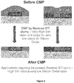
- Figure 1 displays two applications, as examples, in which the Reverse STI CMP composition is used to polish off the SiN layer and then stop on the Silicon Oxide layer. After this Reverse STI CMP step, the semiconductor substrate is further processed.
- the present disclosure provides stable compositions that show very high selectivities of SiN to silicon oxide by achieving nearly zero silicon oxide MRRs.
- the main body of the disclosure discusses the unique technologies that distinguish this disclosure from prior art.
- the subject-matter of the present invention is defined in claims 1-14 as attached.
- the present disclosure relates to stable aqueous slurries that can selectively polish silicon nitride films and nearly stop (or polish at very low rates) on silicon oxide films. More particularly, the present disclosure relates to a polishing composition comprising an anionic abrasive, a nitride removal rate enhancer comprising a carboxyl or a carboxylate group, water, and optionally, an anionic polymer.
- the pH of the polishing composition is in the 2 to 6.5 range.
- the compositions of the present disclosure can also be diluted to form a polishing composition without any deterioration in performance on dilution. This disclosure also discusses methods for polishing semiconductor substrates using the aforementioned polishing compositions.
- nitride removal rate enhancers and anionic abrasives alone do not display this unique behavior.
- currently available slurries might use non-ionic colloidal silica or a cationic abrasive in combination with acid, and thus none of these slurries display unique properties as stated in i), ii) and iii), and displayed by this disclosure.
- the term "nitride removal rate enhancer" indicates a compound that comprises a carboxyl or carboxylate group.
- polishing compositions and concentrates discussed in this disclosure contrast with currently available contemporary slurries in providing performance sustenance on current generation integrated circuit substrates whereas, simultaneously displaying marked advantages for next generation substrates and integration schemes.
- the composition of the present disclosure can successfully and efficiently remove silicon nitride layers with very high selectivity over the oxide layers. This composition can be used for reverse STI processes, clearing etch stop layers, hard masks and many other semiconductor processing applications wherein a relatively high silicon nitride MRR and concomitant almost no MRR on silicon oxide (stop on oxide) layer is required.
- composition of the present disclosure can stop on Ta/TaN or low k/ultra-low k dielectric (SiCOH) films, a feature which will enable polishing other barrier metals while stopping on Ta/TaN or SiCOH layers for many new integration schemes.
- SiCOH low k/ultra-low k dielectric
- the present disclosure provides a polishing composition.
- the composition comprises an anionic abrasive, a nitride removal rate enhancer comprising a carboxylic acid or a carboxyl/carboxylate group for increasing silicon nitride rates, water, and optionally, an anionic polymer.
- the polishing composition has a pH of 2 to 6.5.
- the present disclosure provides a polishing method, comprising applying a polishing composition to a substrate having silicon nitride on its surface, and removing at least a portion of the silicon nitride from the substrate at a first rate, by bringing a pad into contact with the substrate and moving the pad in relation to the substrate.
- the composition comprises an anionic abrasive, a nitride removal rate enhancer comprising a carboxylic acid or a carboxyl/carboxylate group for increasing silicon nitride rates, water, and optionally, an anionic polymer.
- the polishing composition has a pH of 2 to 6.5.
- the present disclosure provides a polishing composition that polishes silicon nitride with high selectivity over the oxide layers.
- the embodiment also provides the method of using the same.
- the polishing composition comprises an anionic abrasive, a nitride removal rate enhancer, pH adjustor, water and/or anionic polymer.
- the pH of the polishing composition is from 2.0 to 6.5.
- the embodiment also provides polishing methods of using the same.
- the present disclosure provides a polishing composition having a broad pH operation range where silicon nitride is polished with high selectivity over the oxide.
- This embodiment also provides the polishing method of using the same.
- the polishing composition comprises an anionic abrasive, a nitride removal rate enhancer, pH adjustor, water and/or anionic polymer.
- the pH of the polishing composition is 2.0 to 6.5.
- the present disclosure provides a polishing composition having a long shelf life, with respect to the usable time period and/or expiration date of the composition.
- the mean particle size MPS, measured by Malvern tool
- MPS mean particle size
- the present disclosure provides a polishing composition having a novel P*V (Pressure * Velocity) response property, wherein a silicon nitride layer of the substrate to be polished exhibits Prestonian behavior while an oxide layer exhibits Non-Prestonian behavior.
- P*V Pressure * Velocity
- This embodiment covers and confirms items i) Beneficial Charge Interactions, and ii) SiN rate and selectivity Enhancement.
- the present disclosure provides a polishing composition that can polish silicon nitride with a high selectivity over the silicon oxide, and produce oxide with very low defectivity post polishing.
- the embodiment also provides the polishing method of using the same.
- the present disclosure provides a polishing composition that can be used for other metal CMP applications, including Co, Cu, W, Ta, TaN or a combination thereof.
- the compositions of the present disclosure can be diluted at the point of use (POU) (i.e., before going on the polishing tool) without changing the CMP performance.
- the concentrated polishing composition can be 2X of POU.
- CMP is performed by diluting the 2X with water, to reach other chemicals' concentration at POU of 1X formulated slurry, there is no deterioration in performance of the concentrate formulation (2X) versus the diluted formulation (1X).
- More concentrated polishing compositions might be prepared using similar methodology.
- the present disclosure provides polishing compositions as well as methods of polishing substrates using the same.
- the polishing composition comprises (a) an anionic abrasive, (b) a nitride removal rate enhancer, (c) water, and, optionally, (d) an anionic polymer.
- the polishing composition has a pH of 2 to 6.5.
- the polishing composition of the present disclosure has a high selectivity of polishing silicon nitride over silicon oxide films during the CMP of substrates comprising silicon nitride and silicon oxide.
- the compositions of the present disclosure can also be diluted without sacrificing performance.
- the present disclosure also provides a polishing method (CMP) of using the polishing composition to polish semiconductor substrates.
- CMP polishing method
- the present disclosure provides a method for polishing silicon nitride with high selectivity to silicon oxide.
- the polishing composition can also be used for applications that need to polish cobalt, copper, or other metals, and other dielectric films such as polycrystalline silicon and low k/ultra-low k dielectric (SiCOH) films.
- the polishing composition comprises an anionic abrasive according to claim 1.
- Anionic abrasives are colloidal abrasives that have been imparted with a negative charge and show negative potential values (in mV) in Zeta Potential plots.
- Non-ionic abrasives are modified into anionic abrasives by attaching anionic groups to some of the abrasive grains. This modification to produce an anionic abrasive may be by chemical bonding or by physically forming self-assembled multiple monolayers on top of the silica grains, or by physical adsorption of the anionic groups on the surface of silica grains.
- the preferred method to form the anionic abrasive is with chemical bonding and it is typically done by reacting the abrasive with a compound of generic formulation -O x -Y-(CH 2 ) z -Anionic group, wherein the x and z integer values can vary, and Y is either alumina, silica, titania, ceria, zirconia, co-formed products thereof, or mixtures thereof (depending on the type of abrasive).
- the "Anionic group” may be an acid such as sulfonic acid, phosphoric acid, carboxylic acid, or anionic salts of any of these acids.
- anionic abrasives are available from the following vendors - anionic ceria from Solvay of Belgium, anionic alumina from Evonik Industries of Germany, and anionic silica from Fuso Chemical Co., Ltd. of Japan.
- anionic abrasive is used to mean negatively-charged abrasives. These include the afore-mentioned commercially available anionic abrasives. They also include in-house chemical modification of non-ionic abrasives by anionic groups (such as acid immobilization), physical modifications by multiple monolayer formation or physical surface adsorption, or any other suitable methods to impart the desired negative charge. These negatively charged abrasives are used in the present polishing compositions with a plurality of chemicals, to obtain very high and selective SiN removal rates versus other dielectric materials.
- Zeta Potential is defined as the potential difference between the liquid dispersion medium, and the stationary layer of fluid attached to the dispersed colloidal particle.
- the Zeta Potential of solutions can be measured by commercially available tools such as the AcoustoSizer II made by Colloidal Dynamics, or Malvern Instruments tools that work by dynamic light scattering.
- the Zeta Potential is particularly useful in determining colloidal dispersion stability.
- a general guideline would be as follows: Zeta Potential (mV) Stability (witch time) of Colloidal Dispersion from 0 to ⁇ 5 Immediate coagulation, gelling and settling from ⁇ 5 to ⁇ 15 Less stable from ⁇ 15 to ⁇ 30 Moderately stable from ⁇ 30 to ⁇ 60 Good stability More than ⁇ 60 Excellent stability
- Zeta potential is related to particle surface charge. Negative zeta potential indicates that the particle surface is negatively charged (anionic) in the dispersion, and vice versa for cationic abrasive (positively charged). In order to maintain the stability of particle dispersion, it is preferred that the absolute value of zeta potential is larger than at least 10 mV (see table).
- the anionic abrasive has a zeta potential in the range of -10 mV to -100 mV, and preferred of -15 mV to -70 mV.
- the polishing composition has a zeta potential in the range of -5 mV to -100 mV , preferably -10 mV to -100 mV, and most preferred of-15 mV to -70 mV.
- the charge of the composition can also be measured by its conductivity.
- the polishing composition can have a conductivity in the preferred range of 0.1 to 10 milli-Siemens per centimeter (mS/cm), or any subranges therebetween, or 0.5 to 5 mS/cm, or any subranges therebetween.
- the anionic abrasive may be present in an amount of from 0.01 wt% to 30 wt%, based on the total weight of the composition, from 0.05 wt% to 15 wt%, based on the total weight of the composition, from 0.1 wt% to 10 wt%, based on the total weight of the composition, or any subranges therebetween.
- the polishing composition of the present disclosure in addition to anionic abrasives, has a nitride removal rate enhancer which, as discussed above, comprises a carboxyl group or a carboxylate group or ion.
- Suitable nitride removal rate enhancers include carboxylic acids such as formic acid, acetic acid, malonic acid, citric acid, propionic acid, malic acid, adipic acid, succinic acid, lactic acid, or any combinations thereof.
- nitride removal rate enhancers that are not necessarily carboxylic acids include potassium acetate, potassium citrate, amino acetic acid, phenoxyacetic acid, tetrahydrofurancarboxylic acid, diglycolic acid, glyceric acid, tricine, benzoic acid, or any combinations thereof.
- the nitride removal rate enhancer may be present in an amount of from 0.01 wt% to 10 wt%, based on the total weight of the composition, from 0.01 wt% to 5 wt%, based on the total weight of the composition, from 0.03 wt% to 3 wt%, based on the total weight of the composition, or any subranges therebetween.
- the polishing composition may optionally contain an anionic polymer.
- the anionic polymer can help in dielectric surface passivation and reducing defectivity post polishing.
- the anionic polymer is preferably sulfonate (-SO 3 - ) based or phosphate based (-PO 4 3- ) and contains hydrocarbon groups.
- the anionic polymer is an anionic surfactant.
- sulfonate/sulfate based anionic surfactants are lauryl ether sulfate, and sulfate based Triton surfactants from Dow Chemical such as TRITON Q-15, XN-45S, and W-30 series.
- phosphate based anionic surfactants/polymers are the Triton series from Dow Chemical such as TRITON H-55, and H-66.
- the anionic polymer may be present in an amount of from 1 ppm to 5 wt%, based on the total weight of the composition, from 1 ppm to 10000 ppm, based on the total weight of the composition, from 1 ppm to 2000 ppm, based on the total weight of the composition, or any subranges therebetween.
- the polishing composition can have a base acting as a pH adjustor.
- the base pH adjustor helps in taking the composition pH to its operating pH value.
- the base used to adjust the pH can be any suitable one, such as potassium hydroxide, ammonium hydroxide, sodium hydroxide, cesium hydroxide, triethanol ammine, tetrabutyl ammonium hydroxide, tetramethyl ammonium hydroxide, or any combinations thereof.
- the pH of the composition of the present disclosure is from 2.0 to 6.5, or any subranges therebetween.
- the pH can also be from 3.0 to 6.0, or any subranges therebetween, or from 3.4 to 5.75, or any subranges therebetween.
- the pH can be measured using a pH meter from the company Thermo Fisher Scientific.
- the particle sizes of the claimed anionic abrasives can have a mean particle size of about 1 nm to 1000 nm, more preferably about 1 nm to 200 nm, and most preferred of about 1 nm to 50 nm, or any subranges thereof.
- a smaller particle size has the advantage of preferentially giving lower TEOS MRRs, and thus improving the overall selectivity of SiN to TEOS.
- Particle size in this disclosure is the mean particle size (MPS) determined by dynamic light scattering techniques.
- the mean particle size can be measured by using a Malvern, a commercial dynamic light scattering tool from Malvern Instruments Ltd.
- compositions of the present disclosure are discussed in combination with polishing SiN, silicon nitride.
- present compositions might also be used to polish silicon carbide (SiC), silicon carbide nitride (SiC x N y ), polysilicon, and other nitride containing materials selectively over silicon oxides (e.g., TEOS).
- the compositions may also be used to selectively polish SiN over silicon oxide containing dielectric materials such as low-k dielectric (SiC x O y H z ), and ultra-low k (ULK) dielectric (SiC x O y H z ) materials.
- dielectric materials such as low-k dielectric (SiC x O y H z ), and ultra-low k (ULK) dielectric (SiC x O y H z ) materials.
- Some common examples of low-k and ULK dielectric materials are Black Diamond I and II, respectively, from Applied Materials.
- This example demonstrates the effect of desired additives for enhancing silicon nitride material removal rates.
- the polishing composition primarily comprises 1 wt% anionic abrasive, several acids as nitride removal rate enhancers, potassium hydroxide as pH adjustor, and water as a liquid carrier.
- the control sample in Table 1 doesn't have acid, whilst others have the same molar amount of the acid additive.
- an Applied Materials Mirra CMP polisher was used with a downforce of 3 psi and a flow rate of 175 mL/min to polish 8 inch silicon nitride and silicon oxide wafers. TABLE 1. Normalized Removal Rate vs.
- the results in Table 1 showed that silicon nitride RR is low without adding an acid into the polishing composition (see Control).
- An acid with a carboxyl group such as acetic acid, propionic acid, or malonic acid significantly increased silicon nitride RR to about 8 to 11 times the Control (without the rate enhancer additive).
- Other acids without a carboxyl group such as nitric acid or phosphoric acid, also increase silicon nitride removal rate, but not as effectively as that of an additive with a carboxyl group.
- the silicon oxide (in this example, TEOS) RR is less than 40 A/min for all the samples in table 1, and near to 0 A/min for most cases.
- the polishing composition in table 2 comprises 1% anionic abrasive, and nitride removal rate enhancer. Potassium hydroxide was used to adjust the pH to the operating pH shown in Table 2. For all examples, an Applied Materials' Mirra CMP polisher was used with a downforce of 3 psi and a flow rate of 175 mL/min to polish 8 inch silicon nitride and silicon oxide wafers.
- the present disclosure clearly shows the novelty of the present composition in being capable of polishing silicon nitride films at very high rates over a broad pH processing/operating window ( Fig. 2 ).
- the prior art does not reveal a composition that is capable of doing so.
- This performance of the polishing compositions in the disclosure might be associated with the relatively similar (fixed value) negative zeta potential of anionic modified particles over a wide pH range, which provides similar electrostatic attractive forces to the silicon nitride wafers (which have positive zeta potential), and thus maintains a similar silicon nitride RR over the entire acidic pH range.
- This unique behavior is again coming from the synergistic action of the anionic abrasive in combination with the nitride removal rate enhancer.
- anionic abrasives have a relatively fixed constant negative zeta potential value over the entire 3 - 10 pH range.
- the fixed value may be any number in between -20 mV to -70 mV depending on the type and size of abrasive.
- an anionic alumina abrasive might have a fixed -35 mV zeta potential value for the entire 3 - 10 pH range.
- the zeta potential value is very different at different pH values in the acidic pH range.
- colloidal silica has a zeta potential value of +10 mV at pH 3, 0 mV at pH 4, and -10 mV at pH 5. So, conversely, not only does the SiN RR become inconsistent due to unfavorable electrostatic forces at different pH values for non-ionic silica (prior art); this different zeta potential value at very narrow pH interims also leads to slurry stability issues (shelf life/expiration date) with time. The unique zeta potential behavior and its consequence on composition stability are discussed further in the composition stability section (Example 3 below).
- CMP compositions should be stable/ usable over time. Inasmuch, the compositions should have an expiration date of at least 6 months to a year at the very least. Instability in CMP compositions can be gauged by an increase in the Mean Particle Size (MPS) of the abrasive grains used in the composition. If there is a growth in abrasive MPS with time, it means that the composition is unstable. This growth in MPS primarily occurs due to the composition containing the abrasive not being a stable colloidal dispersion.
- MPS Mean Particle Size
- composition stability is seen in zeta potential plots of the slurries, wherein, if any composition has zeta potential values within the ⁇ 10 mV range, it is considered unstable and characterized by a growth in MPS with time due to particles agglomerating.
- the synergistic use of anionic abrasive with nitride enhancer molecules increases composition stability and this example demonstrates the same.
- the increase in mean particle size of the abrasives in the composition also causes increase in the defectivity and/or changes in RR during CMP. This therefore results in inconsistent planarization performance which is unacceptable from the customer point of view. Therefore, it is highly desirable that the polishing compositions show stable mean particle size over a prolonged time period.
- the polishing compositions comprise anionic silica and non-ionic (normal) silica, and both had the same MPS of normalized value of 100 at day 0 (Sample 3A & 3E).
- the silica abrasive anionic vs. non-ionic
- all other chemical compositions such as nitride enhancer and pH adjustor are the same.
- Table 3 clearly shows that the polishing composition comprising anionic silica abrasive showed stable MPS over 330 days whereas the polishing composition comprising non-ionic (normal) silica abrasive had an MPS increase of over 4 times in only 80 days (normalized MPS value of 436 after 80 days versus 100 at 0 days).
- anionic modified silica provides long term MPS stability for the polishing compositions as shown in this example. This implies stable industrial compositions for slurries using anionic abrasives and long shelf-life/ expiration dates.
- TABLE 3 Mean particle size comparison of the polishing compositions Sample Abrasive Type Days in Storage pH Normalized MPS 3A Anionic silica abrasive 0 5 100 3B 100 5 99.4 3C 220 5 98.6 3D 330 5 98.9 3E Non-ionic (normal) 0 5 100 3F silica abrasive 80 5 436
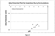
- a further gauge of stability is the zeta potential values of the slurries.
- Figure 3 shows the zeta potential of the optimized inventive compositions. As can be seen from the Figure, the zeta potential of all slurries falls between -20 & -40 mV, clearly indicating that all these slurries are highly stable colloidal dispersions in the 2-7 pH range. Recall that the farther away from zero the zeta potential values are the more stable the dispersions are.
- non-ionic (normal) silica containing dispersions in the acidic pH regime have zeta potential values within the ⁇ 10 mV range, indicating unstable compositions as was confirmed from the study shown in table 3 which shows MPS growth for such slurries.
- the polishing composition comprises anionic abrasive, a nitride removal rate enhancer, a pH adjustor, and water.
- the optimized composition might also include an anionic surfactant.
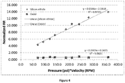
- An Applied Materials RefleXion LK CMP polishing tool was used to polish silicon nitride and TEOS wafers at different polishing pressure (P) and velocity (V) by using the inventive polishing composition.
- Figure 4 shows this unique Non-Prestonian behavior of the present CMP composition on silicon oxide films.
- silicon nitride RR showed linear response (Prestonian) to the polishing P*V process conditions with an R 2 value larger than 0.9; P*V almost had no impact on the silicon oxide RR (Non-Prestonian behavior) and the R 2 value is close to 0.
- This is a very novel property unique only to the composition disclosed in this disclosure.
- a polishing composition had very low oxide RR (near to zero), and the oxide RR were not sensitive to polishing pressure/downforce, this could solve the oxide RR increase issue on pattern wafers.
- the inventive polishing composition of this disclosure would certainly meet the critical requirement of achieving low oxide RR and high silicon nitride RR on patterned wafers, and thus to maintain the high selectivity of silicon nitride RR to oxide RR, as elucidated by this example.
- Defectivity is an important parameter during the chip manufacturing process, and it is preferred to have very low defectivity in every step of CMP so as to have high yield of chip dies. Specifically, for applications involving polishing silicon nitride and oxide with high selectivity, it is preferred that the defectivity on the oxide layer is low because in most applications all of the nitride is removed and the polishing stops as soon as the oxide layer is revealed.
- the example here demonstrates polishing compositions with high selectivity of silicon nitride to oxide, and very low oxide defectivity post polishing.
- the polishing composition primarily comprises anionic abrasive particles and nitride removal rate enhancer.
- some of the inventive compositions optionally contain an anionic polymeric surfactant molecule.
- the surfactant can help to reduce defectivity, and the data in Table 4 make this function of the anionic surfactant more apparent.
- 4B and 4C contain anionic surfactant molecules and have lesser defectivity than the 4A composition that does not contain any surfactants.
- all the inventive compositions have lesser defectivity values than our commercial copper barrier composition (see Table 4).
- the ultra-low defectivity on silicon oxide for the inventive compositions might be attributed (in part) to the ultra-low oxide polishing RR ( ⁇ 40 A/min) of these polishing compositions.
- the polishing composition primarily comprises an anionic abrasive, an agent with a carboxylate group for increasing silicon nitride RR, and optionally an anionic surfactant.
- an Applied Materials Mirra CMP polisher was used with a downforce of 3psi and a flow rate of 175 mL/min to polish 8 inch wafers of selected materials such as silicon nitride, silicon oxide (e.g., TEOS), Co, Cu, W, Ta, and TaN.
- Table 5 shows that the polishing compositions not only showed high selectivity of removing silicon nitride over silicon oxide, but also had very low removal RR on Ta and TaN (this attribute is desirable).
- inventive polishing compositions also achieved very high Co RR, at times as high as 3000 A/min.
- inventive polishing compositions can also be used for applications that need to polish silicon nitride or Co or both SiN and Co at very high polishing rates (and/or with high selectivity to oxide films).
- metal Removal RR with Polishing Compositions Sample Anionic Surfactant Normalized RR Silicon nitride Oxide Co Cu W Ta TaN 5A No 11.779 0.265 62.500 2.568 2.636 0.453 0.475 5B Yes 11.451 0.358 56.318 3.182 1.773 0.281 0.335
- polishing composition can be prepared as concentrates, and then be diluted (with water) at the point of use (POU) for polishing without any deterioration in polishing performance.
- POU point of use
- Table 6 shows polishing composition 6A and 6B, where 6B is the 2X concentrated version of 6A of each composition component except for water.
- 6B is the 2X concentrated version of 6A of each composition component except for water.
- an Applied Materials Mirra CMP polisher was used with a downforce of 3psi and a flow rate of 175 mL/min to polish 8 inch silicon nitride and TEOS wafers.
- the silicon nitride and silicon oxide (TEOS) RR from 6B after 2X dilution is almost the same as that of 6A.
- a 3X or higher concentrated version can be prepared of the inventive composition using similar methodology. TABLE 6. Concentrated vs. non-concentrated version Sample Concentrated version Normalized Silicon nitride RR Normalized Silicon Oxide RR 6A No 12.628 0.053 6B 2X 12.556 0.025
Description
- The present disclosure relates to polishing compositions, and methods for polishing semiconductor substrates using the same. More particularly, this disclosure relates to polishing compositions and methods for selectively polishing silicon nitride films over other dielectric films in semiconductor substrates containing multiple dielectric and metal films.
- The semiconductor industry is continually driven to improve chip performance by further miniaturization of devices by process and integration innovations. Chemical Mechanical Polishing/Planarization (CMP) is a powerful technology as it makes many complex integration schemes at the transistor level possible, thereby increasing chip density. Not surprisingly, there are a multitude of new CMP steps and requirements at the Front End of Line (FEOL) transistor fabrication step. These steps are new CMP requirements; quite different from the traditional shallow trench isolation (STI) and oxide polishing steps. These "exotic" FEOL CMP steps and processes started gaining attention (when compared to Back End of Line (BEOL) CMP) after the introduction of high-k metal gate technology at 45nm and FinFET technology at 22nm chip production by the Intel Corporation. Particularly, in many of these advanced integration schemes, silicon nitride (SiN) films are used as an Etch stop layer, capping material, and Hard Mask. In addition, SiN is also used as a diffusion or passivation layer, spacer material, and additional liner. In all such schemes, the SiN is used in combination with other dielectric films such as silicon oxide (e.g., TEOS) and poly-silicon. Thus, the chip manufacturing steps involving such integration schemes require selective polishing or removal of SiN films without removing the other dielectric material (such as TEOS). Therefore, for such kind of CMP polishing steps, slurries with very high and selective removal of SiN to silicon oxide films are required as most patterned wafers contain both the dielectric films at different density and feature size.
- Other schemes, in which a composition that selectively polishes SiN over silicon oxide (e.g., TEOS) is required, are the "Reverse STI processes" and replacement of "Classic Etch Back processes." In the language of the field, a SiN selective composition over silicon oxide implies a CMP composition that polishes SiN films at very high Material Removal Rates (MRRs) and simultaneously polishes silicon oxide at very low (and near to zero) MRRs thereby removing SiN selectively versus silicon oxide films. For example, a STI composition displays very high silicon oxide rates and very low SiN MRRs. Conversely, a "Reverse STI" composition displays very high SiN rates and very low silicon oxide MRRs, or, in other words, polishes SiN selectively versus silicon oxide films in pattern structures involving both the films.
- The same properties are shown on blanket wafers which contain only an individual film - high SiN rates on blanket SiN wafers and low (to zero) oxide rates on blanket TEOS wafers. However, at times, the selectivity is higher on blanket wafers than observed on patterned wafers. In addition to Reverse STI processes, the SiN selective slurries are now being used in CMP processes that replace Etching processes in schemes involving removal of SiN by "Classic Etch Back processes." In such schemes, it is desirable to utilize CMP rather than Etching methods because CMP delivers better defectivity and higher planarity on the substrate surface; to meet the ever increasing stringent requirements of semiconductor manufacturing.
-
Figure 1 displays two applications, as examples, in which the Reverse STI CMP composition is used to polish off the SiN layer and then stop on the Silicon Oxide layer. After this Reverse STI CMP step, the semiconductor substrate is further processed. - The present disclosure provides stable compositions that show very high selectivities of SiN to silicon oxide by achieving nearly zero silicon oxide MRRs. The main body of the disclosure discusses the unique technologies that distinguish this disclosure from prior art.
- The subject-matter of the present invention is defined in claims 1-14 as attached. The present disclosure relates to stable aqueous slurries that can selectively polish silicon nitride films and nearly stop (or polish at very low rates) on silicon oxide films. More particularly, the present disclosure relates to a polishing composition comprising an anionic abrasive, a nitride removal rate enhancer comprising a carboxyl or a carboxylate group, water, and optionally, an anionic polymer. The pH of the polishing composition is in the 2 to 6.5 range. The compositions of the present disclosure can also be diluted to form a polishing composition without any deterioration in performance on dilution. This disclosure also discusses methods for polishing semiconductor substrates using the aforementioned polishing compositions.
- The synergistic use of a negatively charged (anionic) abrasive and the nitride removal rate enhancer having a carboxyl or carboxylate group in the same composition provides advantages not found in currently available slurries. Among others, these benefits are:
- i) Beneficial Charge Interactions - the anionic abrasive, being negatively charged, repels the negatively charged silicon oxide wafer surface and is drawn toward the positively charged silicon nitride (SiN) wafer surface. The repulsion forces with silicon oxide wafers decrease the material removal rates (MRRs) of silicon oxide during polishing, and the attractive forces with the SiN wafer surface help in increasing the SiN MRRs. This generates a highly selective SiN:silicon oxide composition, in the 2 to 6.5 operating pH range.
- ii) SiN rate and selectivity Enhancement - The nitride removal rate enhancer acts as a SiN rate enhancer. The rate & selectivity enhancement of SiN is further magnified due to the synergistic effect of i) & ii) arising due to the simultaneous presence of both the anionic abrasive and enhancer.
- iii) Composition Stability in acidic pH - Colloidal silica is known to have stability issues (with time) in the 3-6 pH range due to the Zeta potential being near to zero (typical range is within ± 15 mV). However, anionic silica has Zeta potential much farther away from zero (typical range is -20 mV to -60 mV) and remains a stable colloidal dispersion in the entire acidic pH regime. Therefore, the inventive composition containing anionic silica is also stable within the entire operating pH range of 2 to 6.5. This unique stability behavior is not shown by any of the prior art due to the abrasive being non-ionic or cationic in the prior art.
- The nitride removal rate enhancers and anionic abrasives alone do not display this unique behavior. Also, currently available slurries might use non-ionic colloidal silica or a cationic abrasive in combination with acid, and thus none of these slurries display unique properties as stated in i), ii) and iii), and displayed by this disclosure. As used in the present disclosure, the term "nitride removal rate enhancer" indicates a compound that comprises a carboxyl or carboxylate group.
- The polishing compositions and concentrates discussed in this disclosure contrast with currently available contemporary slurries in providing performance sustenance on current generation integrated circuit substrates whereas, simultaneously displaying marked advantages for next generation substrates and integration schemes. The composition of the present disclosure can successfully and efficiently remove silicon nitride layers with very high selectivity over the oxide layers. This composition can be used for reverse STI processes, clearing etch stop layers, hard masks and many other semiconductor processing applications wherein a relatively high silicon nitride MRR and concomitant almost no MRR on silicon oxide (stop on oxide) layer is required. Furthermore, the composition of the present disclosure can stop on Ta/TaN or low k/ultra-low k dielectric (SiCOH) films, a feature which will enable polishing other barrier metals while stopping on Ta/TaN or SiCOH layers for many new integration schemes.
- Thus, in one embodiment, the present disclosure provides a polishing composition. The composition comprises an anionic abrasive, a nitride removal rate enhancer comprising a carboxylic acid or a carboxyl/carboxylate group for increasing silicon nitride rates, water, and optionally, an anionic polymer. The polishing composition has a pH of 2 to 6.5.
- In another embodiment, the present disclosure provides a polishing method, comprising applying a polishing composition to a substrate having silicon nitride on its surface, and removing at least a portion of the silicon nitride from the substrate at a first rate, by bringing a pad into contact with the substrate and moving the pad in relation to the substrate. The composition comprises an anionic abrasive, a nitride removal rate enhancer comprising a carboxylic acid or a carboxyl/carboxylate group for increasing silicon nitride rates, water, and optionally, an anionic polymer. The polishing composition has a pH of 2 to 6.5.
- Thus, in one embodiment, the present disclosure provides a polishing composition that polishes silicon nitride with high selectivity over the oxide layers. The embodiment also provides the method of using the same. The polishing composition comprises an anionic abrasive, a nitride removal rate enhancer, pH adjustor, water and/or anionic polymer. The pH of the polishing composition is from 2.0 to 6.5. The embodiment also provides polishing methods of using the same.
- In another embodiment, the present disclosure provides a polishing composition having a broad pH operation range where silicon nitride is polished with high selectivity over the oxide. This embodiment also provides the polishing method of using the same. The polishing composition comprises an anionic abrasive, a nitride removal rate enhancer, pH adjustor, water and/or anionic polymer. The pH of the polishing composition is 2.0 to 6.5.
- In yet another embodiment, the present disclosure provides a polishing composition having a long shelf life, with respect to the usable time period and/or expiration date of the composition. Particularly, the mean particle size (MPS, measured by Malvern tool) is stable for about a year or longer. In other words, item iii) discussed above, a composition stability in acidic pH is covered by this embodiment.
- In another embodiment, the present disclosure provides a polishing composition having a novel P*V (Pressure * Velocity) response property, wherein a silicon nitride layer of the substrate to be polished exhibits Prestonian behavior while an oxide layer exhibits Non-Prestonian behavior. This embodiment covers and confirms items i) Beneficial Charge Interactions, and ii) SiN rate and selectivity Enhancement.
- In another embodiment, the present disclosure provides a polishing composition that can polish silicon nitride with a high selectivity over the silicon oxide, and produce oxide with very low defectivity post polishing. The embodiment also provides the polishing method of using the same.
- In another embodiment, the present disclosure provides a polishing composition that can be used for other metal CMP applications, including Co, Cu, W, Ta, TaN or a combination thereof.
- In yet another embodiment, the compositions of the present disclosure can be diluted at the point of use (POU) (i.e., before going on the polishing tool) without changing the CMP performance. For example, the concentrated polishing composition can be 2X of POU. When CMP is performed by diluting the 2X with water, to reach other chemicals' concentration at POU of 1X formulated slurry, there is no deterioration in performance of the concentrate formulation (2X) versus the diluted formulation (1X). More concentrated polishing compositions might be prepared using similar methodology.
-
-
Fig 1 is a schematic diagram of Reverse STI polishing applications that require selective polishing of SiN at very high rates and simultaneous low rates of silicon oxide. The reverse STI composition presented in this disclosure would be used in these and related applications. -
Fig 2 is a graph showing a broad pH range of operation for the polishing compositions of the present disclosure, with high selectivity of silicon nitride over silicon oxide. -
Fig 3 is a Zeta Potential Plot for the compositions of the present disclosure. -
Fig 4 shows P*V responses of the polishing composition of the present disclosure. - The present disclosure provides polishing compositions as well as methods of polishing substrates using the same. The polishing composition comprises (a) an anionic abrasive, (b) a nitride removal rate enhancer, (c) water, and, optionally, (d) an anionic polymer. The polishing composition has a pH of 2 to 6.5. The polishing composition of the present disclosure has a high selectivity of polishing silicon nitride over silicon oxide films during the CMP of substrates comprising silicon nitride and silicon oxide. The compositions of the present disclosure can also be diluted without sacrificing performance. The present disclosure also provides a polishing method (CMP) of using the polishing composition to polish semiconductor substrates. Particularly, the present disclosure provides a method for polishing silicon nitride with high selectivity to silicon oxide. The polishing composition can also be used for applications that need to polish cobalt, copper, or other metals, and other dielectric films such as polycrystalline silicon and low k/ultra-low k dielectric (SiCOH) films.
- The polishing composition comprises an anionic abrasive according to
claim 1. Anionic abrasives are colloidal abrasives that have been imparted with a negative charge and show negative potential values (in mV) in Zeta Potential plots. Non-ionic abrasives are modified into anionic abrasives by attaching anionic groups to some of the abrasive grains. This modification to produce an anionic abrasive may be by chemical bonding or by physically forming self-assembled multiple monolayers on top of the silica grains, or by physical adsorption of the anionic groups on the surface of silica grains. - The preferred method to form the anionic abrasive is with chemical bonding and it is typically done by reacting the abrasive with a compound of generic formulation
-Ox-Y-(CH2)z-Anionic group,
wherein the x and z integer values can vary, and Y is either alumina, silica, titania, ceria, zirconia, co-formed products thereof, or mixtures thereof (depending on the type of abrasive). The "Anionic group" may be an acid such as sulfonic acid, phosphoric acid, carboxylic acid, or anionic salts of any of these acids. Commercial anionic abrasives are available from the following vendors - anionic ceria from Solvay of Belgium, anionic alumina from Evonik Industries of Germany, and anionic silica from Fuso Chemical Co., Ltd. of Japan. In the present disclosure, "anionic abrasive" is used to mean negatively-charged abrasives. These include the afore-mentioned commercially available anionic abrasives. They also include in-house chemical modification of non-ionic abrasives by anionic groups (such as acid immobilization), physical modifications by multiple monolayer formation or physical surface adsorption, or any other suitable methods to impart the desired negative charge. These negatively charged abrasives are used in the present polishing compositions with a plurality of chemicals, to obtain very high and selective SiN removal rates versus other dielectric materials. - One way to measure the charge of the anionic abrasives is with Zeta Potential. In colloidal systems, Zeta Potential is defined as the potential difference between the liquid dispersion medium, and the stationary layer of fluid attached to the dispersed colloidal particle. The Zeta Potential of solutions can be measured by commercially available tools such as the AcoustoSizer II made by Colloidal Dynamics, or Malvern Instruments tools that work by dynamic light scattering. The Zeta Potential is particularly useful in determining colloidal dispersion stability. A general guideline would be as follows:
Zeta Potential (mV) Stability (witch time) of Colloidal Dispersion from 0 to ±5 Immediate coagulation, gelling and settling from ±5 to ±15 Less stable from ±15 to ±30 Moderately stable from ±30 to ±60 Good stability More than ±60 Excellent stability - Furthermore, Zeta potential is related to particle surface charge. Negative zeta potential indicates that the particle surface is negatively charged (anionic) in the dispersion, and vice versa for cationic abrasive (positively charged). In order to maintain the stability of particle dispersion, it is preferred that the absolute value of zeta potential is larger than at least 10 mV (see table). In this invention, the anionic abrasive has a zeta potential in the range of -10 mV to -100 mV, and preferred of -15 mV to -70 mV. Furthermore, the polishing composition has a zeta potential in the range of -5 mV to -100 mV , preferably -10 mV to -100 mV, and most preferred of-15 mV to -70 mV.
- The charge of the composition can also be measured by its conductivity. The polishing composition can have a conductivity in the preferred range of 0.1 to 10 milli-Siemens per centimeter (mS/cm), or any subranges therebetween, or 0.5 to 5 mS/cm, or any subranges therebetween.
- The anionic abrasive may be present in an amount of from 0.01 wt% to 30 wt%, based on the total weight of the composition, from 0.05 wt% to 15 wt%, based on the total weight of the composition, from 0.1 wt% to 10 wt%, based on the total weight of the composition, or any subranges therebetween.
- The polishing composition of the present disclosure, in addition to anionic abrasives, has a nitride removal rate enhancer which, as discussed above, comprises a carboxyl group or a carboxylate group or ion. Suitable nitride removal rate enhancers include carboxylic acids such as formic acid, acetic acid, malonic acid, citric acid, propionic acid, malic acid, adipic acid, succinic acid, lactic acid, or any combinations thereof. Other suitable nitride removal rate enhancers that are not necessarily carboxylic acids include potassium acetate, potassium citrate, amino acetic acid, phenoxyacetic acid, tetrahydrofurancarboxylic acid, diglycolic acid, glyceric acid, tricine, benzoic acid, or any combinations thereof.
- The nitride removal rate enhancer may be present in an amount of from 0.01 wt% to 10 wt%, based on the total weight of the composition, from 0.01 wt% to 5 wt%, based on the total weight of the composition, from 0.03 wt% to 3 wt%, based on the total weight of the composition, or any subranges therebetween.
- The polishing composition may optionally contain an anionic polymer. The anionic polymer can help in dielectric surface passivation and reducing defectivity post polishing. The anionic polymer is preferably sulfonate (-SO3 -) based or phosphate based (-PO4 3-) and contains hydrocarbon groups. In one embodiment, the anionic polymer is an anionic surfactant. Some examples of sulfonate/sulfate based anionic surfactants are lauryl ether sulfate, and sulfate based Triton surfactants from Dow Chemical such as TRITON Q-15, XN-45S, and W-30 series. Some examples of phosphate based anionic surfactants/polymers are the Triton series from Dow Chemical such as TRITON H-55, and H-66.
- When present, the anionic polymer may be present in an amount of from 1 ppm to 5 wt%, based on the total weight of the composition, from 1 ppm to 10000 ppm, based on the total weight of the composition, from 1 ppm to 2000 ppm, based on the total weight of the composition, or any subranges therebetween.
- In addition to the above components, the polishing composition can have a base acting as a pH adjustor. The base pH adjustor helps in taking the composition pH to its operating pH value. The base used to adjust the pH can be any suitable one, such as potassium hydroxide, ammonium hydroxide, sodium hydroxide, cesium hydroxide, triethanol ammine, tetrabutyl ammonium hydroxide, tetramethyl ammonium hydroxide, or any combinations thereof.
- The pH of the composition of the present disclosure is from 2.0 to 6.5, or any subranges therebetween. The pH can also be from 3.0 to 6.0, or any subranges therebetween, or from 3.4 to 5.75, or any subranges therebetween. The pH can be measured using a pH meter from the company Thermo Fisher Scientific.
- With respect to the particle sizes of the claimed anionic abrasives, they can have a mean particle size of about 1 nm to 1000 nm, more preferably about 1 nm to 200 nm, and most preferred of about 1 nm to 50 nm, or any subranges thereof. A smaller particle size has the advantage of preferentially giving lower TEOS MRRs, and thus improving the overall selectivity of SiN to TEOS. Particle size in this disclosure is the mean particle size (MPS) determined by dynamic light scattering techniques. For instance, the mean particle size can be measured by using a Malvern, a commercial dynamic light scattering tool from Malvern Instruments Ltd.
- In the discussion above and in the following examples, the compositions of the present disclosure are discussed in combination with polishing SiN, silicon nitride. However, present compositions might also be used to polish silicon carbide (SiC), silicon carbide nitride (SiCxNy), polysilicon, and other nitride containing materials selectively over silicon oxides (e.g., TEOS). The compositions may also be used to selectively polish SiN over silicon oxide containing dielectric materials such as low-k dielectric (SiCxOyHz), and ultra-low k (ULK) dielectric (SiCxOyHz) materials. Some common examples of low-k and ULK dielectric materials are Black Diamond I and II, respectively, from Applied Materials.
- Examples are provided to further illustrate the capabilities of the polishing compositions and methods of the present disclosure. The provided examples are not intended and should not be construed to limit the scope of the present disclosure.
- This example demonstrates the effect of desired additives for enhancing silicon nitride material removal rates.
- In this example, the polishing composition primarily comprises 1 wt% anionic abrasive, several acids as nitride removal rate enhancers, potassium hydroxide as pH adjustor, and water as a liquid carrier. The control sample in Table 1 doesn't have acid, whilst others have the same molar amount of the acid additive. For all examples, an Applied Materials Mirra CMP polisher was used with a downforce of 3 psi and a flow rate of 175 mL/min to polish 8 inch silicon nitride and silicon oxide wafers.
TABLE 1. Normalized Removal Rate vs. Different Additives Sample Acid POU Anionic Abrasives Wt% Normalized SiN RR Normalized TEOS RR SiN: TEOS Control None 1 1.000 0.063 16 1A Nitric acid 1 5.716 0.867 7 1B Acetic Acid 1 11.182 0.630 18 1C Propionic acid 1 10.966 0.114 97 1D Malonic acid 1 8.920 0.713 13 1E Dequest 2010 1 3.125 0.351 9 1F H2SO4 1 4.619 0.664 7 - The results in Table 1 showed that silicon nitride RR is low without adding an acid into the polishing composition (see Control). An acid with a carboxyl group, such as acetic acid, propionic acid, or malonic acid significantly increased silicon nitride RR to about 8 to 11 times the Control (without the rate enhancer additive). Other acids without a carboxyl group, such as nitric acid or phosphoric acid, also increase silicon nitride removal rate, but not as effectively as that of an additive with a carboxyl group. The silicon oxide (in this example, TEOS) RR is less than 40 A/min for all the samples in table 1, and near to 0 A/min for most cases. This very low oxide RR on TEOS was achieved because the abrasive has small particle size and has anionic surface charge, so the TEOS repels the anionic abrasive and gives low MRRs. Thus, the synergistic effect of combining anionic abrasive with selective carboxylate containing nitride rate enhancer molecules leads to a highly selective SiN (to TEOS) composition displaying high SiN RR and very low TEOS rates.
- This example demonstrates how the composition of the present disclosure operates across a broad pH range.
TABLE 2. Normalized Removal Rate vs. Different pH Abrasive Type Sample pH POU Abrasives wt-% Normalized SiN RR Normalized TEOS RR Anionic abrasive 2A 3.41 1 11.854 0.068 2B 4 1 12.466 0.386 2C 4.5 1 12.474 0.049 2D 4.75 1 12.386 0.111 2E 5 1 12.459 0.136 2F 5.25 1 12.278 0.085 2G 5.5 1 11.988 0.025 2H 5.75 1 9.926 0.249 2I 6 1 7.366 0.036 - The polishing composition in table 2 comprises 1% anionic abrasive, and nitride removal rate enhancer. Potassium hydroxide was used to adjust the pH to the operating pH shown in Table 2. For all examples, an Applied Materials' Mirra CMP polisher was used with a downforce of 3 psi and a flow rate of 175 mL/min to polish 8 inch silicon nitride and silicon oxide wafers.
- As shown in table 2, high silicon nitride RR, around the maximum of ∼ 12 (Normalized) with very low Oxide RR of < 0.386 (Normalized) were obtained for the pH range of 3.4 to 5.5 for the optimized inventive composition. Silicon nitride RR has ∼ 16% reduction after increasing pH to 5.75. Further increase in pH to 6 will cause more reduction in silicon nitride MRRs. The polishing composition in this example showed much broader pH operation range of ∼3 to 5.75 for achieving high silicon nitride RR and low oxide RR. By contrast, in one example of an available slurry in
U.S. Patent No. 7,217,989 , all examples showed narrow pH operation range of 4.5 to 5.0 for achieving high silicon nitride RR. Below or above the pH range of 4.5 to 5.0, silicon nitride MRRs drop more than 30%. - In this Example, the present disclosure clearly shows the novelty of the present composition in being capable of polishing silicon nitride films at very high rates over a broad pH processing/operating window (
Fig. 2 ). The prior art does not reveal a composition that is capable of doing so. This performance of the polishing compositions in the disclosure might be associated with the relatively similar (fixed value) negative zeta potential of anionic modified particles over a wide pH range, which provides similar electrostatic attractive forces to the silicon nitride wafers (which have positive zeta potential), and thus maintains a similar silicon nitride RR over the entire acidic pH range. This unique behavior is again coming from the synergistic action of the anionic abrasive in combination with the nitride removal rate enhancer. This behavior contrasts with prior art, wherein (normal) non-ionic silica particles are used and as pH decreases in acidic pH regime, the zeta potential is less negative or more positive for non-ionic silica, which provides a decreasing electrostatic attractive forces, or even repulsion forces to the silicon nitride wafer surface (which has positive charge), and thereby causes the silicon nitride CMP removal rates reduction. - To further elaborate, anionic abrasives have a relatively fixed constant negative zeta potential value over the entire 3 - 10 pH range. Typically, the fixed value may be any number in between -20 mV to -70 mV depending on the type and size of abrasive. For example, an anionic alumina abrasive might have a fixed -35 mV zeta potential value for the entire 3 - 10 pH range. However, for non-ionic abrasives (used in prior art), the zeta potential value is very different at different pH values in the acidic pH range. For, e.g., colloidal silica has a zeta potential value of +10 mV at
pH 3, 0 mV atpH 4, and -10 mV atpH 5. So, conversely, not only does the SiN RR become inconsistent due to unfavorable electrostatic forces at different pH values for non-ionic silica (prior art); this different zeta potential value at very narrow pH interims also leads to slurry stability issues (shelf life/expiration date) with time. The unique zeta potential behavior and its consequence on composition stability are discussed further in the composition stability section (Example 3 below). - This example shows the effect of anionic silica on the stability of the polishing compositions. In the semiconductor fabrication community, it is well known that CMP compositions should be stable/ usable over time. Inasmuch, the compositions should have an expiration date of at least 6 months to a year at the very least. Instability in CMP compositions can be gauged by an increase in the Mean Particle Size (MPS) of the abrasive grains used in the composition. If there is a growth in abrasive MPS with time, it means that the composition is unstable. This growth in MPS primarily occurs due to the composition containing the abrasive not being a stable colloidal dispersion. Colloidal stability is seen in zeta potential plots of the slurries, wherein, if any composition has zeta potential values within the ± 10 mV range, it is considered unstable and characterized by a growth in MPS with time due to particles agglomerating. The synergistic use of anionic abrasive with nitride enhancer molecules increases composition stability and this example demonstrates the same.
- In addition to composition shelf life issues arising from growth in MPS, the increase in mean particle size of the abrasives in the composition also causes increase in the defectivity and/or changes in RR during CMP. This therefore results in inconsistent planarization performance which is unacceptable from the customer point of view. Therefore, it is highly desirable that the polishing compositions show stable mean particle size over a prolonged time period.
- In table 3, the polishing compositions comprise anionic silica and non-ionic (normal) silica, and both had the same MPS of normalized value of 100 at day 0 (Sample 3A & 3E). In the compositions in table 3, except for the silica abrasive (anionic vs. non-ionic), all other chemical compositions such as nitride enhancer and pH adjustor are the same. Table 3 clearly shows that the polishing composition comprising anionic silica abrasive showed stable MPS over 330 days whereas the polishing composition comprising non-ionic (normal) silica abrasive had an MPS increase of over 4 times in only 80 days (normalized MPS value of 436 after 80 days versus 100 at 0 days). Thus, the use of anionic modified silica provides long term MPS stability for the polishing compositions as shown in this example. This implies stable industrial compositions for slurries using anionic abrasives and long shelf-life/ expiration dates.
TABLE 3. Mean particle size comparison of the polishing compositions Sample Abrasive Type Days in Storage pH Normalized MPS 3A Anionic silica abrasive 0 5 100 3B 100 5 99.4 3C 220 5 98.6 3D 330 5 98.9 3E Non-ionic (normal) 0 5 100 3F silica abrasive 80 5 436 - A further gauge of stability is the zeta potential values of the slurries.
Figure 3 shows the zeta potential of the optimized inventive compositions. As can be seen from the Figure, the zeta potential of all slurries falls between -20 & -40 mV, clearly indicating that all these slurries are highly stable colloidal dispersions in the 2-7 pH range. Recall that the farther away from zero the zeta potential values are the more stable the dispersions are. As already stated, non-ionic (normal) silica containing dispersions in the acidic pH regime (pH 2 to 6) have zeta potential values within the ± 10 mV range, indicating unstable compositions as was confirmed from the study shown in table 3 which shows MPS growth for such slurries. - This example shows the impact of polishing pressure (P, psi) and velocity (V, RPM) on the silicon nitride and silicon oxide (e.g., TEOS) MRRs. The polishing composition comprises anionic abrasive, a nitride removal rate enhancer, a pH adjustor, and water. The optimized composition might also include an anionic surfactant. An Applied Materials RefleXion LK CMP polishing tool was used to polish silicon nitride and TEOS wafers at different polishing pressure (P) and velocity (V) by using the inventive polishing composition.
- In a conventional CMP process, the fundamental equation describing Material Removal Rate is based on Preston's Law which states that Removal Rate (RR) is directly proportional to applied pressure (P - contact pressure between the substrate and polishing platen) and relative velocity (V - rotational speed/rpm of the platen) of the polishing platen.

-
Figure 4 shows this unique Non-Prestonian behavior of the present CMP composition on silicon oxide films. As can be seen inFig. 4 , silicon nitride RR showed linear response (Prestonian) to the polishing P*V process conditions with an R2 value larger than 0.9; P*V almost had no impact on the silicon oxide RR (Non-Prestonian behavior) and the R2 value is close to 0. This is a very novel property unique only to the composition disclosed in this disclosure. This confirms that the unique anionic abrasive plus chemicals package in the composition is not only achieving very high SiN MRRs; concomitantly it is also causing the composition to stop on Oxide - even with increase in Pressure/Velocity/Friction Oxide RR stays same ∼ 0 (seeFig. 4 ). In all prior art, the oxide RR increases as the polishing pressure (or velocity) increases. This non-prestonian response of oxide RR to polishing PV has many benefits in CMP. For instance, one of the issues reported in the prior art (Schlueter & Henry et. al. "High Selectivity Silicon Nitride Slurry for Advanced Technology Node Front End CMP Applications", 18th International Symposium on Chemical-Mechanical Planarization, Aug 11-14, 2013, Lake Placid, NY, USA) is that the oxide RR on patterned wafers tend to be much higher than that on blanket wafer. The main contributor for this issue is that the oxide RR increases with increasing polishing pressure (downforce). Schlueter et al. reported that when their slurry was used to polish patterned wafers comprising both SiN and Oxide features, the smaller oxide features (in areas having very high SiN and very low oxide density in the pattern features) are under much higher local pressure, and therefore showed much higher oxide RR and consequently much lower selectivity to SiN films. Therefore, if a polishing composition had very low oxide RR (near to zero), and the oxide RR were not sensitive to polishing pressure/downforce, this could solve the oxide RR increase issue on pattern wafers. The inventive polishing composition of this disclosure would certainly meet the critical requirement of achieving low oxide RR and high silicon nitride RR on patterned wafers, and thus to maintain the high selectivity of silicon nitride RR to oxide RR, as elucidated by this example. - Defectivity is an important parameter during the chip manufacturing process, and it is preferred to have very low defectivity in every step of CMP so as to have high yield of chip dies. Specifically, for applications involving polishing silicon nitride and oxide with high selectivity, it is preferred that the defectivity on the oxide layer is low because in most applications all of the nitride is removed and the polishing stops as soon as the oxide layer is revealed. The example here demonstrates polishing compositions with high selectivity of silicon nitride to oxide, and very low oxide defectivity post polishing.
- In table 4, the polishing composition primarily comprises anionic abrasive particles and nitride removal rate enhancer. As stated earlier, some of the inventive compositions optionally contain an anionic polymeric surfactant molecule. The surfactant can help to reduce defectivity, and the data in Table 4 make this function of the anionic surfactant more apparent. For instance, 4B and 4C contain anionic surfactant molecules and have lesser defectivity than the 4A composition that does not contain any surfactants. Furthermore, all the inventive compositions have lesser defectivity values than our commercial copper barrier composition (see Table 4). For all examples, an Applied Materials Mirra CMP polisher was used with a downforce of 3psi and a flow rate of 175 mL/min to polish 8 inch silicon nitride and oxide wafers.
TABLE 4. Wafer Defectivity Vs. Polishing Compositions Sample Anionic Surfactant Normalized Silicon Nitride RR Normalized Silicon Oxide RR Defectivity 4A NO 11.779 0.265 60 4B Yes 11.451 0.358 34 4C Yes 11.563 0.545 26 Commercial Slurry Yes 4.545 18.182 100∼200 - The ultra-low defectivity on silicon oxide for the inventive compositions might be attributed (in part) to the ultra-low oxide polishing RR (< 40 A/min) of these polishing compositions.
- In one embodiment, the removal rates of SiN and silicon oxide or polysilicon can satisfy the following equations:


- This example shows that the inventive polishing compositions discussed in this disclosure can also be used for polishing other metals.
- In table 5, the polishing composition primarily comprises an anionic abrasive, an agent with a carboxylate group for increasing silicon nitride RR, and optionally an anionic surfactant. For all examples, an Applied Materials Mirra CMP polisher was used with a downforce of 3psi and a flow rate of 175 mL/min to polish 8 inch wafers of selected materials such as silicon nitride, silicon oxide (e.g., TEOS), Co, Cu, W, Ta, and TaN. Table 5 shows that the polishing compositions not only showed high selectivity of removing silicon nitride over silicon oxide, but also had very low removal RR on Ta and TaN (this attribute is desirable). The inventive polishing compositions also achieved very high Co RR, at times as high as 3000 A/min. Thus, the inventive polishing compositions can also be used for applications that need to polish silicon nitride or Co or both SiN and Co at very high polishing rates (and/or with high selectivity to oxide films).
TABLE 5. Metal Removal RR with Polishing Compositions Sample Anionic Surfactant Normalized RR Silicon nitride Oxide Co Cu W Ta TaN 5A No 11.779 0.265 62.500 2.568 2.636 0.453 0.475 5B Yes 11.451 0.358 56.318 3.182 1.773 0.281 0.335 - This example demonstrates that the polishing composition can be prepared as concentrates, and then be diluted (with water) at the point of use (POU) for polishing without any deterioration in polishing performance. Typically, customers prefer slurry concentrates so as to reduce freight/shipping costs and have advantageous overall slurry pricing.
- Table 6 shows polishing composition 6A and 6B, where 6B is the 2X concentrated version of 6A of each composition component except for water. For all examples, an Applied Materials Mirra CMP polisher was used with a downforce of 3psi and a flow rate of 175 mL/min to polish 8 inch silicon nitride and TEOS wafers. The silicon nitride and silicon oxide (TEOS) RR from 6B after 2X dilution is almost the same as that of 6A. For people skilled in the art, a 3X or higher concentrated version can be prepared of the inventive composition using similar methodology.
TABLE 6. Concentrated vs. non-concentrated version Sample Concentrated version Normalized Silicon nitride RR Normalized Silicon Oxide RR 6A No 12.628 0.053 6B 2X 12.556 0.025 - While the present disclosure has been described with reference to one or more exemplary embodiments, it will be understood by those skilled in the art that various changes may be made and equivalents may be substituted for elements thereof without departing from the scope of the present disclosure. Variations of the preferred embodiments mentioned herein may become apparent to those of ordinary skill in the art upon reading the foregoing descriptions. In addition, many modifications may be made to adapt a particular situation or material to the teachings of the disclosure without departing from the scope thereof. Therefore, it is intended that the present disclosure not be limited to the particular embodiment(s) disclosed as the best mode contemplated, but that the disclosure will include all embodiments falling within the scope of the appended claims.
Claims (14)
- A polishing composition, comprising:a) an anionic abrasiveselected from the group consisting of alumina, silica, titania, ceria, zirconia, co-formed products thereof, and mixtures thereof, wherein the anionic abrasive has a zeta potential in the range of -10 mV to-100 mV;b) a nitride removal rate enhancer comprising a carboxylic acid or a carboxyl/carboxylate group for increasing silicon nitride rates; andc) water;wherein the polishing composition has a pH of 2 to 6.5, and
wherein the polishing composition has a zeta potential in the range of -5 mV to -100 mV. - The polishing composition of claim 1, wherein the anionic abrasive is anionic colloidal alumina.
- The polishing composition of claim 2, wherein the anionic abrasive is selected from the group consisting of anionic colloidal silica, acid immobilized non-ionic silica to generate anionic silica, and electrostatically negatively charged colloidal mixtures thereof.
- The polishing composition of claim 1,
wherein the mean particle size of the anionic abrasive is 1 nm to 1000 nm, or
wherein the mean particle size of the anionic abrasive is 1 nm to 50 nm. - The polishing composition of claim 1, wherein the anionic abrasive has a preferred zeta potential in the range of -15 mV to -70 mV.
- The polishing composition of claim 1,
wherein the polishing composition has a zeta potential in the range of -15 mV to -70 mV, or
wherein the composition has a conductivity in the range of 0.1 to 10 milli-Siemens per centimeter (mS/cm), or
wherein the abrasive is present in the composition in the amount of 0.1 wt% to 30 wt%, based on the total weight of the composition. - The polishing composition of claim 1,
wherein the nitride removal rate enhancer is selected from the group consisting of gluconic acid, lactic acid, citric acid, tartaric acid, malic acid, glycolic acid, malonic acid, formic acid, oxalic acid, acetic acid, propionic acid, peracetic acid, succinic acid, lactic acid, potassium acetate, potassium citrate, amino acetic acid, phenoxyacetic acid, tetrahydrofurancarboxylic acid, diglycolic acid, glyceric acid, tricine, histidine, tyrosine, benzoic acid, and any mixtures thereof. - The polishing composition of claim 1,
wherein the nitride removal rate enhancer is present in the composition in an amount of 0.01 wt% to 20 wt%, based on the total weight of the composition, or
wherein the nitride removal rate enhancer is present in the concentrate in an amount of 0.01 wt% to 3 wt%, based on the total weight of the composition. - The polishing composition according to claim 1,
further comprising an anionic polymer,
preferably wherein the anionic polymer is an anionic surfactant with an average molar mass of 120 g/mol or greater. - The polishing composition according to claim 9,
wherein the anionic surfactant contains a sulfonate (-SO3) or phosphate (-PO4) moiety and additionally hydrocarbon groups and combinations thereof, or
wherein the anionic surfactant is selected from the group consisting of an alkylbenzene sulfonic acid, an alkylbenzene sulfonate, an alkyl sulfate, an alkyl ether sulfate and any combinations thereof, or
wherein the anionic surfactant is in the amount of 0.001 wt% to 5 wt%, based on the total weight of the composition. - The polishing composition according to claim 1,
further comprising a base as a pH adjustor,
preferably wherein the base is selected from the group consisting of potassium hydroxide, ammonium hydroxide, triethanol ammine, tetrabutyl ammonium hydroxide, tetramethyl ammonium hydroxide, sodium hydroxide, cesium hydroxide, and any combinations thereof. - The polishing composition of claim 1,
wherein the concentrate can be diluted to 2X, 3X or greater at point of use (POU) before polishing, without any deterioration in polishing performance of POU when compared to the polishing composition concentrate. - A polishing method, comprising:applying a polishing composition to a substrate having silicon nitride on its surface; andremoving at least a portion of the silicon nitride from the substrate at a first rate, by bringing a pad into contact with the substrate and moving the pad in relation to the substrate,wherein the composition comprises:a) an anionic abrasive selected from the group consisting of alumina, silica, titania, ceria, zirconia, co-formed products thereof, and mixtures thereof, wherein the anionic abrasive has a zeta potential in the range of -10 mV to-100 mV;b) a nitride removal rate enhancer comprising a carboxylic acid or a carboxyl/carboxylate group for increasing silicon nitride rates; andc) water;wherein the polishing composition has a pH of 2 to 6.5, and
wherein the polishing composition has a zeta potential in the range of -5 mV to -100 mV,
preferably wherein the substrate further comprises at least one of silicon oxide and polysilicon on the surface, and the method further comprises removing said at least one of silicon oxide and polysilicon at a second rate, wherein said first rate is greater than said second rate. - A method for producing a semiconductor device, comprising the polishing method of claim 13.
Applications Claiming Priority (1)
| Application Number | Priority Date | Filing Date | Title |
|---|---|---|---|
| US14/245,286 US9583359B2 (en) | 2014-04-04 | 2014-04-04 | Polishing compositions and methods for selectively polishing silicon nitride over silicon oxide films |
Publications (2)
| Publication Number | Publication Date |
|---|---|
| EP2927294A1 EP2927294A1 (en) | 2015-10-07 |
| EP2927294B1 true EP2927294B1 (en) | 2017-08-02 |
Family
ID=53039177
Family Applications (1)
| Application Number | Title | Priority Date | Filing Date |
|---|---|---|---|
| EP15158633.6A Active EP2927294B1 (en) | 2014-04-04 | 2015-03-11 | Polishing compositions and methods for selectively polishing silicon nitride over silicon oxide films |
Country Status (5)
| Country | Link |
|---|---|
| US (2) | US9583359B2 (en) |
| EP (1) | EP2927294B1 (en) |
| JP (1) | JP6437870B2 (en) |
| KR (1) | KR101899948B1 (en) |
| TW (1) | TWI611009B (en) |
Families Citing this family (19)
| Publication number | Priority date | Publication date | Assignee | Title |
|---|---|---|---|---|
| WO2014070461A1 (en) * | 2012-11-02 | 2014-05-08 | Lawrence Livermore National Security, Llc | Method for preventing agglomeration of charged colloids without loss of surface activity |
| US9583359B2 (en) * | 2014-04-04 | 2017-02-28 | Fujifilm Planar Solutions, LLC | Polishing compositions and methods for selectively polishing silicon nitride over silicon oxide films |
| JP2016207973A (en) * | 2015-04-28 | 2016-12-08 | 株式会社東芝 | Manufacturing method of semiconductor device |
| JP6974336B2 (en) * | 2016-02-16 | 2021-12-01 | シーエムシー マテリアルズ,インコーポレイティド | Polishing method for III-V materials |
| WO2017169808A1 (en) * | 2016-03-30 | 2017-10-05 | 株式会社フジミインコーポレーテッド | Polishing composition |
| US10344186B2 (en) * | 2016-06-22 | 2019-07-09 | Cabot Microelectronics Corporation | Polishing composition comprising an amine-containing surfactant |
| EP3526298A4 (en) | 2016-10-17 | 2020-06-24 | Cabot Microelectronics Corporation | Cmp compositions selective for oxide and nitride with improved dishing and pattern selectivity |
| CN106672892A (en) * | 2016-12-21 | 2017-05-17 | 中国电子科技集团公司第五十五研究所 | Method for reducing depressed deformation of sacrificial layer in three-dimensional stacking in chemical mechanical polishing |
| US10294399B2 (en) * | 2017-01-05 | 2019-05-21 | Cabot Microelectronics Corporation | Composition and method for polishing silicon carbide |
| WO2018217628A1 (en) * | 2017-05-25 | 2018-11-29 | Fujifilm Planar Solutions, LLC | Chemical mechanical polishing slurry for cobalt applications |
| US10170335B1 (en) * | 2017-09-21 | 2019-01-01 | Rohm And Haas Electronic Materials Cmp Holdings, Inc. | Chemical mechanical polishing method for cobalt |
| US10377921B2 (en) * | 2017-09-21 | 2019-08-13 | Rohm and Haas Electronics Materials CMP Holdings, Inc. | Chemical mechanical polishing method for cobalt |
| US10584265B2 (en) | 2017-09-28 | 2020-03-10 | Rohm And Haas Electronic Materials Cmp Holdings, Inc. | Aqueous silica slurry and amine carboxylic acid compositions selective for nitride removal in polishing and methods of using them |
| US11186748B2 (en) * | 2017-09-28 | 2021-11-30 | Rohm And Haas Electronic Materials Cmp Holdings, Inc. | Aqueous anionic functional silica slurry and amine carboxylic acid compositions for selective nitride removal in polishing and methods of using them |
| US10428241B2 (en) * | 2017-10-05 | 2019-10-01 | Fujifilm Electronic Materials U.S.A., Inc. | Polishing compositions containing charged abrasive |
| WO2019181399A1 (en) * | 2018-03-23 | 2019-09-26 | 富士フイルム株式会社 | Polishing liquid and chemical mechanical polishing method |
| JP7002635B2 (en) * | 2018-03-23 | 2022-01-20 | 富士フイルム株式会社 | Polishing liquid and chemical mechanical polishing method |
| KR20200086141A (en) | 2019-01-08 | 2020-07-16 | 삼성전자주식회사 | Etchant composition for silicon nitride and method of fabricating semiconductor device |
| JP2022529113A (en) * | 2019-04-17 | 2022-06-17 | シーエムシー マテリアルズ,インコーポレイティド | Surface coated grinding particles for tungsten buff applications |
Family Cites Families (38)
| Publication number | Priority date | Publication date | Assignee | Title |
|---|---|---|---|---|
| JPH11176773A (en) | 1997-12-12 | 1999-07-02 | Toshiba Corp | Polishing method |
| TW510917B (en) | 1998-02-24 | 2002-11-21 | Showa Denko Kk | Abrasive composition for polishing semiconductor device and method for manufacturing semiconductor device using same |
| JP3957924B2 (en) * | 1999-06-28 | 2007-08-15 | 株式会社東芝 | CMP polishing method |
| US6783432B2 (en) * | 2001-06-04 | 2004-08-31 | Applied Materials Inc. | Additives for pressure sensitive polishing compositions |
| US6811470B2 (en) * | 2001-07-16 | 2004-11-02 | Applied Materials Inc. | Methods and compositions for chemical mechanical polishing shallow trench isolation substrates |
| US6776810B1 (en) * | 2002-02-11 | 2004-08-17 | Cabot Microelectronics Corporation | Anionic abrasive particles treated with positively charged polyelectrolytes for CMP |
| US6866793B2 (en) * | 2002-09-26 | 2005-03-15 | University Of Florida Research Foundation, Inc. | High selectivity and high planarity dielectric polishing |
| US7063597B2 (en) * | 2002-10-25 | 2006-06-20 | Applied Materials | Polishing processes for shallow trench isolation substrates |
| US7390744B2 (en) * | 2004-01-29 | 2008-06-24 | Applied Materials, Inc. | Method and composition for polishing a substrate |
| US7390748B2 (en) * | 2004-08-05 | 2008-06-24 | International Business Machines Corporation | Method of forming a polishing inhibiting layer using a slurry having an additive |
| US20070037892A1 (en) * | 2004-09-08 | 2007-02-15 | Irina Belov | Aqueous slurry containing metallate-modified silica particles |
| JP4954462B2 (en) | 2004-10-19 | 2012-06-13 | 株式会社フジミインコーポレーテッド | Composition for selective polishing of silicon nitride film and polishing method using the same |
| US7504044B2 (en) | 2004-11-05 | 2009-03-17 | Cabot Microelectronics Corporation | Polishing composition and method for high silicon nitride to silicon oxide removal rate ratios |
| WO2006133249A2 (en) * | 2005-06-06 | 2006-12-14 | Advanced Technology Materials, Inc. | Integrated chemical mechanical polishing composition and process for single platen processing |
| US20070048991A1 (en) | 2005-08-23 | 2007-03-01 | Taiwan Semiconductor Manufacturing Co., Ltd. | Copper interconnect structures and fabrication method thereof |
| US20070209287A1 (en) * | 2006-03-13 | 2007-09-13 | Cabot Microelectronics Corporation | Composition and method to polish silicon nitride |
| US7653117B2 (en) | 2006-03-16 | 2010-01-26 | Harris Corporation | Method for decoding digital data in a frequency hopping communication system |
| KR100832993B1 (en) * | 2006-04-14 | 2008-05-27 | 주식회사 엘지화학 | Adjuvant for chemical mechanical polishing slurry |
| US20070254485A1 (en) * | 2006-04-28 | 2007-11-01 | Daxin Mao | Abrasive composition for electrochemical mechanical polishing |
| US8759216B2 (en) | 2006-06-07 | 2014-06-24 | Cabot Microelectronics Corporation | Compositions and methods for polishing silicon nitride materials |
| KR101396853B1 (en) | 2007-07-06 | 2014-05-20 | 삼성전자주식회사 | Slurry Composition for Polishing Silicon Nitride, Method of Polishing a Silicon Nitride Layer Using the Slurry Composition and Method of Manufacturing a Semiconductor Device Using the Slurry Composition |
| CN101802125B (en) | 2007-09-21 | 2013-11-06 | 卡伯特微电子公司 | Polishing composition and method utilizing abrasive particles treated with an aminosilane |
| WO2009058274A1 (en) * | 2007-10-29 | 2009-05-07 | Ekc Technology, Inc. | Chemical mechanical polishing and wafer cleaning composition comprising amidoxime compounds and associated method for use |
| DE102007062572A1 (en) | 2007-12-22 | 2009-06-25 | Evonik Degussa Gmbh | Cerium oxide and colloidal silica containing dispersion |
| US8425797B2 (en) * | 2008-03-21 | 2013-04-23 | Cabot Microelectronics Corporation | Compositions for polishing aluminum/copper and titanium in damascene structures |
| JP5467804B2 (en) * | 2008-07-11 | 2014-04-09 | 富士フイルム株式会社 | Polishing liquid for silicon nitride and polishing method |
| JP5261065B2 (en) * | 2008-08-08 | 2013-08-14 | シャープ株式会社 | Manufacturing method of semiconductor device |
| EP2329519B1 (en) * | 2008-09-26 | 2013-10-23 | Rhodia Opérations | Abrasive compositions for chemical mechanical polishing and methods for using same |
| JP5371416B2 (en) * | 2008-12-25 | 2013-12-18 | 富士フイルム株式会社 | Polishing liquid and polishing method |
| WO2011093153A1 (en) * | 2010-02-01 | 2011-08-04 | Jsr株式会社 | Aqueous dispersion for chemical mechanical polishing, and chemical mechanical polishing method using same |
| JP5554121B2 (en) * | 2010-03-31 | 2014-07-23 | 富士フイルム株式会社 | Polishing liquid and polishing method |
| JP5601922B2 (en) * | 2010-07-29 | 2014-10-08 | 富士フイルム株式会社 | Polishing liquid and polishing method |
| JP5695367B2 (en) | 2010-08-23 | 2015-04-01 | 株式会社フジミインコーポレーテッド | Polishing composition and polishing method using the same |
| US20120161320A1 (en) | 2010-12-23 | 2012-06-28 | Akolkar Rohan N | Cobalt metal barrier layers |
| US8623766B2 (en) * | 2011-09-20 | 2014-01-07 | Cabot Microelectronics Corporation | Composition and method for polishing aluminum semiconductor substrates |
| JP5957292B2 (en) * | 2012-05-18 | 2016-07-27 | 株式会社フジミインコーポレーテッド | Polishing composition, polishing method using the same, and substrate manufacturing method |
| US8778211B2 (en) * | 2012-07-17 | 2014-07-15 | Cabot Microelectronics Corporation | GST CMP slurries |
| US9583359B2 (en) * | 2014-04-04 | 2017-02-28 | Fujifilm Planar Solutions, LLC | Polishing compositions and methods for selectively polishing silicon nitride over silicon oxide films |
-
2014
- 2014-04-04 US US14/245,286 patent/US9583359B2/en active Active
-
2015
- 2015-03-11 EP EP15158633.6A patent/EP2927294B1/en active Active
- 2015-03-13 TW TW104108090A patent/TWI611009B/en active
- 2015-03-31 KR KR1020150044959A patent/KR101899948B1/en active IP Right Grant
- 2015-04-03 JP JP2015076924A patent/JP6437870B2/en active Active
- 2015-09-17 US US14/857,310 patent/US9558959B2/en active Active
Non-Patent Citations (1)
| Title |
|---|
| None * |
Also Published As
| Publication number | Publication date |
|---|---|
| JP6437870B2 (en) | 2018-12-12 |
| US20160079080A1 (en) | 2016-03-17 |
| US9583359B2 (en) | 2017-02-28 |
| EP2927294A1 (en) | 2015-10-07 |
| KR20150115645A (en) | 2015-10-14 |
| TW201542785A (en) | 2015-11-16 |
| TWI611009B (en) | 2018-01-11 |
| KR101899948B1 (en) | 2018-09-19 |
| US20150284593A1 (en) | 2015-10-08 |
| JP2015201644A (en) | 2015-11-12 |
| US9558959B2 (en) | 2017-01-31 |
Similar Documents
| Publication | Publication Date | Title |
|---|---|---|
| EP2927294B1 (en) | Polishing compositions and methods for selectively polishing silicon nitride over silicon oxide films | |
| US11674056B2 (en) | Polishing compositions containing charged abrasive | |
| US6749488B2 (en) | Chemical mechanical polishing slurry composition for polishing conductive and non-conductive layers on semiconductor wafers | |
| TWI658133B (en) | Polishing slurry composition | |
| KR101053712B1 (en) | Combinations, Methods, and Compositions for Chemical Mechanical Planarization of Tungsten-Containing Substrates | |
| JP2000160141A (en) | Grinding composition and grinding method using the same | |
| CN110088359B (en) | High temperature CMP compositions and methods of use thereof | |
| US9190286B2 (en) | Composition for advanced node front-and-back-end of line chemical mechanical polishing | |
| US8652295B2 (en) | CMP tool implementing cyclic self-limiting CM process | |
| KR101660384B1 (en) | Polishing slurry composition |
Legal Events
| Date | Code | Title | Description |
|---|---|---|---|
| PUAI | Public reference made under article 153(3) epc to a published international application that has entered the european phase |
Free format text: ORIGINAL CODE: 0009012 |
|
| AK | Designated contracting states |
Kind code of ref document: A1 Designated state(s): AL AT BE BG CH CY CZ DE DK EE ES FI FR GB GR HR HU IE IS IT LI LT LU LV MC MK MT NL NO PL PT RO RS SE SI SK SM TR |
|
| AX | Request for extension of the european patent |
Extension state: BA ME |
|
| 17P | Request for examination filed |
Effective date: 20160331 |
|
| RBV | Designated contracting states (corrected) |
Designated state(s): AL AT BE BG CH CY CZ DE DK EE ES FI FR GB GR HR HU IE IS IT LI LT LU LV MC MK MT NL NO PL PT RO RS SE SI SK SM TR |
|
| GRAP | Despatch of communication of intention to grant a patent |
Free format text: ORIGINAL CODE: EPIDOSNIGR1 |
|
| STAA | Information on the status of an ep patent application or granted ep patent |
Free format text: STATUS: GRANT OF PATENT IS INTENDED |
|
| INTG | Intention to grant announced |
Effective date: 20170119 |
|
| GRAJ | Information related to disapproval of communication of intention to grant by the applicant or resumption of examination proceedings by the epo deleted |
Free format text: ORIGINAL CODE: EPIDOSDIGR1 |
|
| STAA | Information on the status of an ep patent application or granted ep patent |
Free format text: STATUS: REQUEST FOR EXAMINATION WAS MADE |
|
| INTC | Intention to grant announced (deleted) | ||
| GRAR | Information related to intention to grant a patent recorded |
Free format text: ORIGINAL CODE: EPIDOSNIGR71 |
|
| GRAS | Grant fee paid |
Free format text: ORIGINAL CODE: EPIDOSNIGR3 |
|
| STAA | Information on the status of an ep patent application or granted ep patent |
Free format text: STATUS: GRANT OF PATENT IS INTENDED |
|
| GRAA | (expected) grant |
Free format text: ORIGINAL CODE: 0009210 |
|
| STAA | Information on the status of an ep patent application or granted ep patent |
Free format text: STATUS: THE PATENT HAS BEEN GRANTED |
|
| AK | Designated contracting states |
Kind code of ref document: B1 Designated state(s): AL AT BE BG CH CY CZ DE DK EE ES FI FR GB GR HR HU IE IS IT LI LT LU LV MC MK MT NL NO PL PT RO RS SE SI SK SM TR |
|
| INTG | Intention to grant announced |
Effective date: 20170623 |
|
| REG | Reference to a national code |
Ref country code: CH Ref legal event code: EP Ref country code: AT Ref legal event code: REF Ref document number: 914459 Country of ref document: AT Kind code of ref document: T Effective date: 20170815 |
|
| REG | Reference to a national code |
Ref country code: IE Ref legal event code: FG4D |
|
| REG | Reference to a national code |
Ref country code: DE Ref legal event code: R096 Ref document number: 602015003806 Country of ref document: DE |
|
| REG | Reference to a national code |
Ref country code: NL Ref legal event code: FP |
|
| REG | Reference to a national code |
Ref country code: LT Ref legal event code: MG4D |
|
| PG25 | Lapsed in a contracting state [announced via postgrant information from national office to epo] |
Ref country code: HR Free format text: LAPSE BECAUSE OF FAILURE TO SUBMIT A TRANSLATION OF THE DESCRIPTION OR TO PAY THE FEE WITHIN THE PRESCRIBED TIME-LIMIT Effective date: 20170802 Ref country code: NO Free format text: LAPSE BECAUSE OF FAILURE TO SUBMIT A TRANSLATION OF THE DESCRIPTION OR TO PAY THE FEE WITHIN THE PRESCRIBED TIME-LIMIT Effective date: 20171102 Ref country code: LT Free format text: LAPSE BECAUSE OF FAILURE TO SUBMIT A TRANSLATION OF THE DESCRIPTION OR TO PAY THE FEE WITHIN THE PRESCRIBED TIME-LIMIT Effective date: 20170802 Ref country code: SE Free format text: LAPSE BECAUSE OF FAILURE TO SUBMIT A TRANSLATION OF THE DESCRIPTION OR TO PAY THE FEE WITHIN THE PRESCRIBED TIME-LIMIT Effective date: 20170802 Ref country code: FI Free format text: LAPSE BECAUSE OF FAILURE TO SUBMIT A TRANSLATION OF THE DESCRIPTION OR TO PAY THE FEE WITHIN THE PRESCRIBED TIME-LIMIT Effective date: 20170802 |
|
| PG25 | Lapsed in a contracting state [announced via postgrant information from national office to epo] |
Ref country code: PL Free format text: LAPSE BECAUSE OF FAILURE TO SUBMIT A TRANSLATION OF THE DESCRIPTION OR TO PAY THE FEE WITHIN THE PRESCRIBED TIME-LIMIT Effective date: 20170802 Ref country code: RS Free format text: LAPSE BECAUSE OF FAILURE TO SUBMIT A TRANSLATION OF THE DESCRIPTION OR TO PAY THE FEE WITHIN THE PRESCRIBED TIME-LIMIT Effective date: 20170802 Ref country code: IS Free format text: LAPSE BECAUSE OF FAILURE TO SUBMIT A TRANSLATION OF THE DESCRIPTION OR TO PAY THE FEE WITHIN THE PRESCRIBED TIME-LIMIT Effective date: 20171202 Ref country code: LV Free format text: LAPSE BECAUSE OF FAILURE TO SUBMIT A TRANSLATION OF THE DESCRIPTION OR TO PAY THE FEE WITHIN THE PRESCRIBED TIME-LIMIT Effective date: 20170802 Ref country code: BG Free format text: LAPSE BECAUSE OF FAILURE TO SUBMIT A TRANSLATION OF THE DESCRIPTION OR TO PAY THE FEE WITHIN THE PRESCRIBED TIME-LIMIT Effective date: 20171102 Ref country code: ES Free format text: LAPSE BECAUSE OF FAILURE TO SUBMIT A TRANSLATION OF THE DESCRIPTION OR TO PAY THE FEE WITHIN THE PRESCRIBED TIME-LIMIT Effective date: 20170802 Ref country code: GR Free format text: LAPSE BECAUSE OF FAILURE TO SUBMIT A TRANSLATION OF THE DESCRIPTION OR TO PAY THE FEE WITHIN THE PRESCRIBED TIME-LIMIT Effective date: 20171103 |
|
| REG | Reference to a national code |
Ref country code: FR Ref legal event code: PLFP Year of fee payment: 4 |
|
| PG25 | Lapsed in a contracting state [announced via postgrant information from national office to epo] |
Ref country code: CZ Free format text: LAPSE BECAUSE OF FAILURE TO SUBMIT A TRANSLATION OF THE DESCRIPTION OR TO PAY THE FEE WITHIN THE PRESCRIBED TIME-LIMIT Effective date: 20170802 Ref country code: DK Free format text: LAPSE BECAUSE OF FAILURE TO SUBMIT A TRANSLATION OF THE DESCRIPTION OR TO PAY THE FEE WITHIN THE PRESCRIBED TIME-LIMIT Effective date: 20170802 Ref country code: RO Free format text: LAPSE BECAUSE OF FAILURE TO SUBMIT A TRANSLATION OF THE DESCRIPTION OR TO PAY THE FEE WITHIN THE PRESCRIBED TIME-LIMIT Effective date: 20170802 |
|
| REG | Reference to a national code |
Ref country code: DE Ref legal event code: R097 Ref document number: 602015003806 Country of ref document: DE |
|
| PG25 | Lapsed in a contracting state [announced via postgrant information from national office to epo] |
Ref country code: EE Free format text: LAPSE BECAUSE OF FAILURE TO SUBMIT A TRANSLATION OF THE DESCRIPTION OR TO PAY THE FEE WITHIN THE PRESCRIBED TIME-LIMIT Effective date: 20170802 Ref country code: SK Free format text: LAPSE BECAUSE OF FAILURE TO SUBMIT A TRANSLATION OF THE DESCRIPTION OR TO PAY THE FEE WITHIN THE PRESCRIBED TIME-LIMIT Effective date: 20170802 Ref country code: SM Free format text: LAPSE BECAUSE OF FAILURE TO SUBMIT A TRANSLATION OF THE DESCRIPTION OR TO PAY THE FEE WITHIN THE PRESCRIBED TIME-LIMIT Effective date: 20170802 |
|
| PLBE | No opposition filed within time limit |
Free format text: ORIGINAL CODE: 0009261 |
|
| STAA | Information on the status of an ep patent application or granted ep patent |
Free format text: STATUS: NO OPPOSITION FILED WITHIN TIME LIMIT |
|
| 26N | No opposition filed |
Effective date: 20180503 |
|
| PG25 | Lapsed in a contracting state [announced via postgrant information from national office to epo] |
Ref country code: SI Free format text: LAPSE BECAUSE OF FAILURE TO SUBMIT A TRANSLATION OF THE DESCRIPTION OR TO PAY THE FEE WITHIN THE PRESCRIBED TIME-LIMIT Effective date: 20170802 |
|
| REG | Reference to a national code |
Ref country code: CH Ref legal event code: PL |
|
| PG25 | Lapsed in a contracting state [announced via postgrant information from national office to epo] |
Ref country code: MC Free format text: LAPSE BECAUSE OF FAILURE TO SUBMIT A TRANSLATION OF THE DESCRIPTION OR TO PAY THE FEE WITHIN THE PRESCRIBED TIME-LIMIT Effective date: 20170802 |
|
| PG25 | Lapsed in a contracting state [announced via postgrant information from national office to epo] |
Ref country code: LU Free format text: LAPSE BECAUSE OF NON-PAYMENT OF DUE FEES Effective date: 20180311 |
|
| PG25 | Lapsed in a contracting state [announced via postgrant information from national office to epo] |
Ref country code: LI Free format text: LAPSE BECAUSE OF NON-PAYMENT OF DUE FEES Effective date: 20180331 Ref country code: CH Free format text: LAPSE BECAUSE OF NON-PAYMENT OF DUE FEES Effective date: 20180331 |
|
| REG | Reference to a national code |
Ref country code: DE Ref legal event code: R081 Ref document number: 602015003806 Country of ref document: DE Owner name: FUJIFILM ELECTRONIC MATERIALS, NORTH KINGSTON, US Free format text: FORMER OWNER: FUJIFILM PLANAR SOLUTIONS LLC, ADRIAN, MICH., US Ref country code: DE Ref legal event code: R081 Ref document number: 602015003806 Country of ref document: DE Owner name: FUJIFILM ELECTRONIC MATERIALS USA, INC., NORTH, US Free format text: FORMER OWNER: FUJIFILM PLANAR SOLUTIONS LLC, ADRIAN, MICH., US |
|
| REG | Reference to a national code |
Ref country code: DE Ref legal event code: R081 Ref document number: 602015003806 Country of ref document: DE Owner name: FUJIFILM ELECTRONIC MATERIALS, NORTH KINGSTON, US Free format text: FORMER OWNER: FUJIFILM ELECTRONICS MATERIALS U.S.A., INC, NORTH KINGSTON, RI, US Ref country code: DE Ref legal event code: R082 Ref document number: 602015003806 Country of ref document: DE Representative=s name: NOTARBARTOLO & GERVASI GMBH, DE Ref country code: DE Ref legal event code: R081 Ref document number: 602015003806 Country of ref document: DE Owner name: FUJIFILM ELECTRONIC MATERIALS USA, INC., NORTH, US Free format text: FORMER OWNER: FUJIFILM ELECTRONICS MATERIALS U.S.A., INC, NORTH KINGSTON, RI, US |
|
| REG | Reference to a national code |
Ref country code: AT Ref legal event code: PC Ref document number: 914459 Country of ref document: AT Kind code of ref document: T Owner name: FUJIFILM ELECTRONIC MATERIALS U.S.A., INC., US Effective date: 20190506 |
|
| REG | Reference to a national code |
Ref country code: DE Ref legal event code: R082 Ref document number: 602015003806 Country of ref document: DE Representative=s name: NOTARBARTOLO & GERVASI GMBH, DE Ref country code: DE Ref legal event code: R081 Ref document number: 602015003806 Country of ref document: DE Owner name: FUJIFILM ELECTRONIC MATERIALS USA, INC., NORTH, US Free format text: FORMER OWNER: FUJIFILM ELECTRONIC MATERIALS, NORTH KINGSTON, RI, US |
|
| REG | Reference to a national code |
Ref country code: AT Ref legal event code: UEP Ref document number: 914459 Country of ref document: AT Kind code of ref document: T Effective date: 20170802 |
|
| GBPC | Gb: european patent ceased through non-payment of renewal fee |
Effective date: 20190311 |
|
| PG25 | Lapsed in a contracting state [announced via postgrant information from national office to epo] |
Ref country code: MT Free format text: LAPSE BECAUSE OF NON-PAYMENT OF DUE FEES Effective date: 20180311 Ref country code: GB Free format text: LAPSE BECAUSE OF NON-PAYMENT OF DUE FEES Effective date: 20190311 |
|
| PG25 | Lapsed in a contracting state [announced via postgrant information from national office to epo] |
Ref country code: TR Free format text: LAPSE BECAUSE OF FAILURE TO SUBMIT A TRANSLATION OF THE DESCRIPTION OR TO PAY THE FEE WITHIN THE PRESCRIBED TIME-LIMIT Effective date: 20170802 |
|
| PG25 | Lapsed in a contracting state [announced via postgrant information from national office to epo] |
Ref country code: PT Free format text: LAPSE BECAUSE OF FAILURE TO SUBMIT A TRANSLATION OF THE DESCRIPTION OR TO PAY THE FEE WITHIN THE PRESCRIBED TIME-LIMIT Effective date: 20170802 |
|
| PG25 | Lapsed in a contracting state [announced via postgrant information from national office to epo] |
Ref country code: CY Free format text: LAPSE BECAUSE OF FAILURE TO SUBMIT A TRANSLATION OF THE DESCRIPTION OR TO PAY THE FEE WITHIN THE PRESCRIBED TIME-LIMIT Effective date: 20170802 Ref country code: MK Free format text: LAPSE BECAUSE OF NON-PAYMENT OF DUE FEES Effective date: 20170802 Ref country code: HU Free format text: LAPSE BECAUSE OF FAILURE TO SUBMIT A TRANSLATION OF THE DESCRIPTION OR TO PAY THE FEE WITHIN THE PRESCRIBED TIME-LIMIT; INVALID AB INITIO Effective date: 20150311 |
|
| PG25 | Lapsed in a contracting state [announced via postgrant information from national office to epo] |
Ref country code: AL Free format text: LAPSE BECAUSE OF FAILURE TO SUBMIT A TRANSLATION OF THE DESCRIPTION OR TO PAY THE FEE WITHIN THE PRESCRIBED TIME-LIMIT Effective date: 20170802 |
|
| PGFP | Annual fee paid to national office [announced via postgrant information from national office to epo] |
Ref country code: AT Payment date: 20220321 Year of fee payment: 8 |
|
| PGFP | Annual fee paid to national office [announced via postgrant information from national office to epo] |
Ref country code: NL Payment date: 20220326 Year of fee payment: 8 |
|
| PGFP | Annual fee paid to national office [announced via postgrant information from national office to epo] |
Ref country code: IE Payment date: 20230327 Year of fee payment: 9 Ref country code: FR Payment date: 20230327 Year of fee payment: 9 |
|
| PGFP | Annual fee paid to national office [announced via postgrant information from national office to epo] |
Ref country code: IT Payment date: 20230321 Year of fee payment: 9 Ref country code: DE Payment date: 20230329 Year of fee payment: 9 Ref country code: BE Payment date: 20230327 Year of fee payment: 9 |
|
| P01 | Opt-out of the competence of the unified patent court (upc) registered |
Effective date: 20230529 |
|
| REG | Reference to a national code |
Ref country code: NL Ref legal event code: MM Effective date: 20230401 |
|
| REG | Reference to a national code |
Ref country code: AT Ref legal event code: MM01 Ref document number: 914459 Country of ref document: AT Kind code of ref document: T Effective date: 20230311 |
|
| PG25 | Lapsed in a contracting state [announced via postgrant information from national office to epo] |
Ref country code: NL Free format text: LAPSE BECAUSE OF NON-PAYMENT OF DUE FEES Effective date: 20230401 |
|
| PG25 | Lapsed in a contracting state [announced via postgrant information from national office to epo] |
Ref country code: AT Free format text: LAPSE BECAUSE OF NON-PAYMENT OF DUE FEES Effective date: 20230311 |