EP2889681A1 - Curved liquid crystal display - Google Patents
Curved liquid crystal display Download PDFInfo
- Publication number
- EP2889681A1 EP2889681A1 EP14200206.2A EP14200206A EP2889681A1 EP 2889681 A1 EP2889681 A1 EP 2889681A1 EP 14200206 A EP14200206 A EP 14200206A EP 2889681 A1 EP2889681 A1 EP 2889681A1
- Authority
- EP
- European Patent Office
- Prior art keywords
- liquid crystal
- substrate
- crystal display
- color filters
- curved
- Prior art date
- Legal status (The legal status is an assumption and is not a legal conclusion. Google has not performed a legal analysis and makes no representation as to the accuracy of the status listed.)
- Granted
Links
Images


Classifications
-
- G—PHYSICS
- G02—OPTICS
- G02F—OPTICAL DEVICES OR ARRANGEMENTS FOR THE CONTROL OF LIGHT BY MODIFICATION OF THE OPTICAL PROPERTIES OF THE MEDIA OF THE ELEMENTS INVOLVED THEREIN; NON-LINEAR OPTICS; FREQUENCY-CHANGING OF LIGHT; OPTICAL LOGIC ELEMENTS; OPTICAL ANALOGUE/DIGITAL CONVERTERS
- G02F1/00—Devices or arrangements for the control of the intensity, colour, phase, polarisation or direction of light arriving from an independent light source, e.g. switching, gating or modulating; Non-linear optics
- G02F1/01—Devices or arrangements for the control of the intensity, colour, phase, polarisation or direction of light arriving from an independent light source, e.g. switching, gating or modulating; Non-linear optics for the control of the intensity, phase, polarisation or colour
- G02F1/13—Devices or arrangements for the control of the intensity, colour, phase, polarisation or direction of light arriving from an independent light source, e.g. switching, gating or modulating; Non-linear optics for the control of the intensity, phase, polarisation or colour based on liquid crystals, e.g. single liquid crystal display cells
- G02F1/133—Constructional arrangements; Operation of liquid crystal cells; Circuit arrangements
- G02F1/136—Liquid crystal cells structurally associated with a semi-conducting layer or substrate, e.g. cells forming part of an integrated circuit
- G02F1/1362—Active matrix addressed cells
-
- G—PHYSICS
- G02—OPTICS
- G02F—OPTICAL DEVICES OR ARRANGEMENTS FOR THE CONTROL OF LIGHT BY MODIFICATION OF THE OPTICAL PROPERTIES OF THE MEDIA OF THE ELEMENTS INVOLVED THEREIN; NON-LINEAR OPTICS; FREQUENCY-CHANGING OF LIGHT; OPTICAL LOGIC ELEMENTS; OPTICAL ANALOGUE/DIGITAL CONVERTERS
- G02F1/00—Devices or arrangements for the control of the intensity, colour, phase, polarisation or direction of light arriving from an independent light source, e.g. switching, gating or modulating; Non-linear optics
- G02F1/01—Devices or arrangements for the control of the intensity, colour, phase, polarisation or direction of light arriving from an independent light source, e.g. switching, gating or modulating; Non-linear optics for the control of the intensity, phase, polarisation or colour
- G02F1/13—Devices or arrangements for the control of the intensity, colour, phase, polarisation or direction of light arriving from an independent light source, e.g. switching, gating or modulating; Non-linear optics for the control of the intensity, phase, polarisation or colour based on liquid crystals, e.g. single liquid crystal display cells
- G02F1/133—Constructional arrangements; Operation of liquid crystal cells; Circuit arrangements
- G02F1/1333—Constructional arrangements; Manufacturing methods
- G02F1/1343—Electrodes
- G02F1/134309—Electrodes characterised by their geometrical arrangement
- G02F1/134363—Electrodes characterised by their geometrical arrangement for applying an electric field parallel to the substrate, i.e. in-plane switching [IPS]
-
- G—PHYSICS
- G02—OPTICS
- G02F—OPTICAL DEVICES OR ARRANGEMENTS FOR THE CONTROL OF LIGHT BY MODIFICATION OF THE OPTICAL PROPERTIES OF THE MEDIA OF THE ELEMENTS INVOLVED THEREIN; NON-LINEAR OPTICS; FREQUENCY-CHANGING OF LIGHT; OPTICAL LOGIC ELEMENTS; OPTICAL ANALOGUE/DIGITAL CONVERTERS
- G02F1/00—Devices or arrangements for the control of the intensity, colour, phase, polarisation or direction of light arriving from an independent light source, e.g. switching, gating or modulating; Non-linear optics
- G02F1/01—Devices or arrangements for the control of the intensity, colour, phase, polarisation or direction of light arriving from an independent light source, e.g. switching, gating or modulating; Non-linear optics for the control of the intensity, phase, polarisation or colour
- G02F1/13—Devices or arrangements for the control of the intensity, colour, phase, polarisation or direction of light arriving from an independent light source, e.g. switching, gating or modulating; Non-linear optics for the control of the intensity, phase, polarisation or colour based on liquid crystals, e.g. single liquid crystal display cells
- G02F1/133—Constructional arrangements; Operation of liquid crystal cells; Circuit arrangements
- G02F1/1333—Constructional arrangements; Manufacturing methods
- G02F1/133305—Flexible substrates, e.g. plastics, organic film
-
- G—PHYSICS
- G02—OPTICS
- G02F—OPTICAL DEVICES OR ARRANGEMENTS FOR THE CONTROL OF LIGHT BY MODIFICATION OF THE OPTICAL PROPERTIES OF THE MEDIA OF THE ELEMENTS INVOLVED THEREIN; NON-LINEAR OPTICS; FREQUENCY-CHANGING OF LIGHT; OPTICAL LOGIC ELEMENTS; OPTICAL ANALOGUE/DIGITAL CONVERTERS
- G02F1/00—Devices or arrangements for the control of the intensity, colour, phase, polarisation or direction of light arriving from an independent light source, e.g. switching, gating or modulating; Non-linear optics
- G02F1/01—Devices or arrangements for the control of the intensity, colour, phase, polarisation or direction of light arriving from an independent light source, e.g. switching, gating or modulating; Non-linear optics for the control of the intensity, phase, polarisation or colour
- G02F1/13—Devices or arrangements for the control of the intensity, colour, phase, polarisation or direction of light arriving from an independent light source, e.g. switching, gating or modulating; Non-linear optics for the control of the intensity, phase, polarisation or colour based on liquid crystals, e.g. single liquid crystal display cells
- G02F1/133—Constructional arrangements; Operation of liquid crystal cells; Circuit arrangements
- G02F1/1333—Constructional arrangements; Manufacturing methods
- G02F1/133345—Insulating layers
-
- G—PHYSICS
- G02—OPTICS
- G02F—OPTICAL DEVICES OR ARRANGEMENTS FOR THE CONTROL OF LIGHT BY MODIFICATION OF THE OPTICAL PROPERTIES OF THE MEDIA OF THE ELEMENTS INVOLVED THEREIN; NON-LINEAR OPTICS; FREQUENCY-CHANGING OF LIGHT; OPTICAL LOGIC ELEMENTS; OPTICAL ANALOGUE/DIGITAL CONVERTERS
- G02F1/00—Devices or arrangements for the control of the intensity, colour, phase, polarisation or direction of light arriving from an independent light source, e.g. switching, gating or modulating; Non-linear optics
- G02F1/01—Devices or arrangements for the control of the intensity, colour, phase, polarisation or direction of light arriving from an independent light source, e.g. switching, gating or modulating; Non-linear optics for the control of the intensity, phase, polarisation or colour
- G02F1/13—Devices or arrangements for the control of the intensity, colour, phase, polarisation or direction of light arriving from an independent light source, e.g. switching, gating or modulating; Non-linear optics for the control of the intensity, phase, polarisation or colour based on liquid crystals, e.g. single liquid crystal display cells
- G02F1/133—Constructional arrangements; Operation of liquid crystal cells; Circuit arrangements
- G02F1/1333—Constructional arrangements; Manufacturing methods
- G02F1/1335—Structural association of cells with optical devices, e.g. polarisers or reflectors
- G02F1/133509—Filters, e.g. light shielding masks
- G02F1/133512—Light shielding layers, e.g. black matrix
-
- G—PHYSICS
- G02—OPTICS
- G02F—OPTICAL DEVICES OR ARRANGEMENTS FOR THE CONTROL OF LIGHT BY MODIFICATION OF THE OPTICAL PROPERTIES OF THE MEDIA OF THE ELEMENTS INVOLVED THEREIN; NON-LINEAR OPTICS; FREQUENCY-CHANGING OF LIGHT; OPTICAL LOGIC ELEMENTS; OPTICAL ANALOGUE/DIGITAL CONVERTERS
- G02F1/00—Devices or arrangements for the control of the intensity, colour, phase, polarisation or direction of light arriving from an independent light source, e.g. switching, gating or modulating; Non-linear optics
- G02F1/01—Devices or arrangements for the control of the intensity, colour, phase, polarisation or direction of light arriving from an independent light source, e.g. switching, gating or modulating; Non-linear optics for the control of the intensity, phase, polarisation or colour
- G02F1/13—Devices or arrangements for the control of the intensity, colour, phase, polarisation or direction of light arriving from an independent light source, e.g. switching, gating or modulating; Non-linear optics for the control of the intensity, phase, polarisation or colour based on liquid crystals, e.g. single liquid crystal display cells
- G02F1/133—Constructional arrangements; Operation of liquid crystal cells; Circuit arrangements
- G02F1/1333—Constructional arrangements; Manufacturing methods
- G02F1/1335—Structural association of cells with optical devices, e.g. polarisers or reflectors
- G02F1/133509—Filters, e.g. light shielding masks
- G02F1/133514—Colour filters
-
- G—PHYSICS
- G02—OPTICS
- G02F—OPTICAL DEVICES OR ARRANGEMENTS FOR THE CONTROL OF LIGHT BY MODIFICATION OF THE OPTICAL PROPERTIES OF THE MEDIA OF THE ELEMENTS INVOLVED THEREIN; NON-LINEAR OPTICS; FREQUENCY-CHANGING OF LIGHT; OPTICAL LOGIC ELEMENTS; OPTICAL ANALOGUE/DIGITAL CONVERTERS
- G02F1/00—Devices or arrangements for the control of the intensity, colour, phase, polarisation or direction of light arriving from an independent light source, e.g. switching, gating or modulating; Non-linear optics
- G02F1/01—Devices or arrangements for the control of the intensity, colour, phase, polarisation or direction of light arriving from an independent light source, e.g. switching, gating or modulating; Non-linear optics for the control of the intensity, phase, polarisation or colour
- G02F1/13—Devices or arrangements for the control of the intensity, colour, phase, polarisation or direction of light arriving from an independent light source, e.g. switching, gating or modulating; Non-linear optics for the control of the intensity, phase, polarisation or colour based on liquid crystals, e.g. single liquid crystal display cells
- G02F1/133—Constructional arrangements; Operation of liquid crystal cells; Circuit arrangements
- G02F1/1333—Constructional arrangements; Manufacturing methods
- G02F1/1337—Surface-induced orientation of the liquid crystal molecules, e.g. by alignment layers
- G02F1/133753—Surface-induced orientation of the liquid crystal molecules, e.g. by alignment layers with different alignment orientations or pretilt angles on a same surface, e.g. for grey scale or improved viewing angle
-
- G—PHYSICS
- G02—OPTICS
- G02F—OPTICAL DEVICES OR ARRANGEMENTS FOR THE CONTROL OF LIGHT BY MODIFICATION OF THE OPTICAL PROPERTIES OF THE MEDIA OF THE ELEMENTS INVOLVED THEREIN; NON-LINEAR OPTICS; FREQUENCY-CHANGING OF LIGHT; OPTICAL LOGIC ELEMENTS; OPTICAL ANALOGUE/DIGITAL CONVERTERS
- G02F1/00—Devices or arrangements for the control of the intensity, colour, phase, polarisation or direction of light arriving from an independent light source, e.g. switching, gating or modulating; Non-linear optics
- G02F1/01—Devices or arrangements for the control of the intensity, colour, phase, polarisation or direction of light arriving from an independent light source, e.g. switching, gating or modulating; Non-linear optics for the control of the intensity, phase, polarisation or colour
- G02F1/13—Devices or arrangements for the control of the intensity, colour, phase, polarisation or direction of light arriving from an independent light source, e.g. switching, gating or modulating; Non-linear optics for the control of the intensity, phase, polarisation or colour based on liquid crystals, e.g. single liquid crystal display cells
- G02F1/133—Constructional arrangements; Operation of liquid crystal cells; Circuit arrangements
- G02F1/1333—Constructional arrangements; Manufacturing methods
- G02F1/1339—Gaskets; Spacers; Sealing of cells
- G02F1/13394—Gaskets; Spacers; Sealing of cells spacers regularly patterned on the cell subtrate, e.g. walls, pillars
-
- G—PHYSICS
- G02—OPTICS
- G02F—OPTICAL DEVICES OR ARRANGEMENTS FOR THE CONTROL OF LIGHT BY MODIFICATION OF THE OPTICAL PROPERTIES OF THE MEDIA OF THE ELEMENTS INVOLVED THEREIN; NON-LINEAR OPTICS; FREQUENCY-CHANGING OF LIGHT; OPTICAL LOGIC ELEMENTS; OPTICAL ANALOGUE/DIGITAL CONVERTERS
- G02F1/00—Devices or arrangements for the control of the intensity, colour, phase, polarisation or direction of light arriving from an independent light source, e.g. switching, gating or modulating; Non-linear optics
- G02F1/01—Devices or arrangements for the control of the intensity, colour, phase, polarisation or direction of light arriving from an independent light source, e.g. switching, gating or modulating; Non-linear optics for the control of the intensity, phase, polarisation or colour
- G02F1/13—Devices or arrangements for the control of the intensity, colour, phase, polarisation or direction of light arriving from an independent light source, e.g. switching, gating or modulating; Non-linear optics for the control of the intensity, phase, polarisation or colour based on liquid crystals, e.g. single liquid crystal display cells
- G02F1/133—Constructional arrangements; Operation of liquid crystal cells; Circuit arrangements
- G02F1/136—Liquid crystal cells structurally associated with a semi-conducting layer or substrate, e.g. cells forming part of an integrated circuit
- G02F1/1362—Active matrix addressed cells
- G02F1/136209—Light shielding layers, e.g. black matrix, incorporated in the active matrix substrate, e.g. structurally associated with the switching element
-
- G—PHYSICS
- G02—OPTICS
- G02F—OPTICAL DEVICES OR ARRANGEMENTS FOR THE CONTROL OF LIGHT BY MODIFICATION OF THE OPTICAL PROPERTIES OF THE MEDIA OF THE ELEMENTS INVOLVED THEREIN; NON-LINEAR OPTICS; FREQUENCY-CHANGING OF LIGHT; OPTICAL LOGIC ELEMENTS; OPTICAL ANALOGUE/DIGITAL CONVERTERS
- G02F1/00—Devices or arrangements for the control of the intensity, colour, phase, polarisation or direction of light arriving from an independent light source, e.g. switching, gating or modulating; Non-linear optics
- G02F1/01—Devices or arrangements for the control of the intensity, colour, phase, polarisation or direction of light arriving from an independent light source, e.g. switching, gating or modulating; Non-linear optics for the control of the intensity, phase, polarisation or colour
- G02F1/13—Devices or arrangements for the control of the intensity, colour, phase, polarisation or direction of light arriving from an independent light source, e.g. switching, gating or modulating; Non-linear optics for the control of the intensity, phase, polarisation or colour based on liquid crystals, e.g. single liquid crystal display cells
- G02F1/133—Constructional arrangements; Operation of liquid crystal cells; Circuit arrangements
- G02F1/136—Liquid crystal cells structurally associated with a semi-conducting layer or substrate, e.g. cells forming part of an integrated circuit
- G02F1/1362—Active matrix addressed cells
- G02F1/136286—Wiring, e.g. gate line, drain line
-
- G—PHYSICS
- G02—OPTICS
- G02F—OPTICAL DEVICES OR ARRANGEMENTS FOR THE CONTROL OF LIGHT BY MODIFICATION OF THE OPTICAL PROPERTIES OF THE MEDIA OF THE ELEMENTS INVOLVED THEREIN; NON-LINEAR OPTICS; FREQUENCY-CHANGING OF LIGHT; OPTICAL LOGIC ELEMENTS; OPTICAL ANALOGUE/DIGITAL CONVERTERS
- G02F1/00—Devices or arrangements for the control of the intensity, colour, phase, polarisation or direction of light arriving from an independent light source, e.g. switching, gating or modulating; Non-linear optics
- G02F1/01—Devices or arrangements for the control of the intensity, colour, phase, polarisation or direction of light arriving from an independent light source, e.g. switching, gating or modulating; Non-linear optics for the control of the intensity, phase, polarisation or colour
- G02F1/13—Devices or arrangements for the control of the intensity, colour, phase, polarisation or direction of light arriving from an independent light source, e.g. switching, gating or modulating; Non-linear optics for the control of the intensity, phase, polarisation or colour based on liquid crystals, e.g. single liquid crystal display cells
- G02F1/133—Constructional arrangements; Operation of liquid crystal cells; Circuit arrangements
- G02F1/136—Liquid crystal cells structurally associated with a semi-conducting layer or substrate, e.g. cells forming part of an integrated circuit
- G02F1/1362—Active matrix addressed cells
- G02F1/1368—Active matrix addressed cells in which the switching element is a three-electrode device
-
- G—PHYSICS
- G02—OPTICS
- G02F—OPTICAL DEVICES OR ARRANGEMENTS FOR THE CONTROL OF LIGHT BY MODIFICATION OF THE OPTICAL PROPERTIES OF THE MEDIA OF THE ELEMENTS INVOLVED THEREIN; NON-LINEAR OPTICS; FREQUENCY-CHANGING OF LIGHT; OPTICAL LOGIC ELEMENTS; OPTICAL ANALOGUE/DIGITAL CONVERTERS
- G02F1/00—Devices or arrangements for the control of the intensity, colour, phase, polarisation or direction of light arriving from an independent light source, e.g. switching, gating or modulating; Non-linear optics
- G02F1/01—Devices or arrangements for the control of the intensity, colour, phase, polarisation or direction of light arriving from an independent light source, e.g. switching, gating or modulating; Non-linear optics for the control of the intensity, phase, polarisation or colour
- G02F1/13—Devices or arrangements for the control of the intensity, colour, phase, polarisation or direction of light arriving from an independent light source, e.g. switching, gating or modulating; Non-linear optics for the control of the intensity, phase, polarisation or colour based on liquid crystals, e.g. single liquid crystal display cells
- G02F1/133—Constructional arrangements; Operation of liquid crystal cells; Circuit arrangements
- G02F1/1333—Constructional arrangements; Manufacturing methods
- G02F1/1337—Surface-induced orientation of the liquid crystal molecules, e.g. by alignment layers
- G02F1/133742—Surface-induced orientation of the liquid crystal molecules, e.g. by alignment layers for homeotropic alignment
-
- G—PHYSICS
- G02—OPTICS
- G02F—OPTICAL DEVICES OR ARRANGEMENTS FOR THE CONTROL OF LIGHT BY MODIFICATION OF THE OPTICAL PROPERTIES OF THE MEDIA OF THE ELEMENTS INVOLVED THEREIN; NON-LINEAR OPTICS; FREQUENCY-CHANGING OF LIGHT; OPTICAL LOGIC ELEMENTS; OPTICAL ANALOGUE/DIGITAL CONVERTERS
- G02F1/00—Devices or arrangements for the control of the intensity, colour, phase, polarisation or direction of light arriving from an independent light source, e.g. switching, gating or modulating; Non-linear optics
- G02F1/01—Devices or arrangements for the control of the intensity, colour, phase, polarisation or direction of light arriving from an independent light source, e.g. switching, gating or modulating; Non-linear optics for the control of the intensity, phase, polarisation or colour
- G02F1/13—Devices or arrangements for the control of the intensity, colour, phase, polarisation or direction of light arriving from an independent light source, e.g. switching, gating or modulating; Non-linear optics for the control of the intensity, phase, polarisation or colour based on liquid crystals, e.g. single liquid crystal display cells
- G02F1/133—Constructional arrangements; Operation of liquid crystal cells; Circuit arrangements
- G02F1/1333—Constructional arrangements; Manufacturing methods
- G02F1/1337—Surface-induced orientation of the liquid crystal molecules, e.g. by alignment layers
- G02F1/133753—Surface-induced orientation of the liquid crystal molecules, e.g. by alignment layers with different alignment orientations or pretilt angles on a same surface, e.g. for grey scale or improved viewing angle
- G02F1/133757—Surface-induced orientation of the liquid crystal molecules, e.g. by alignment layers with different alignment orientations or pretilt angles on a same surface, e.g. for grey scale or improved viewing angle with different alignment orientations
-
- G—PHYSICS
- G02—OPTICS
- G02F—OPTICAL DEVICES OR ARRANGEMENTS FOR THE CONTROL OF LIGHT BY MODIFICATION OF THE OPTICAL PROPERTIES OF THE MEDIA OF THE ELEMENTS INVOLVED THEREIN; NON-LINEAR OPTICS; FREQUENCY-CHANGING OF LIGHT; OPTICAL LOGIC ELEMENTS; OPTICAL ANALOGUE/DIGITAL CONVERTERS
- G02F1/00—Devices or arrangements for the control of the intensity, colour, phase, polarisation or direction of light arriving from an independent light source, e.g. switching, gating or modulating; Non-linear optics
- G02F1/01—Devices or arrangements for the control of the intensity, colour, phase, polarisation or direction of light arriving from an independent light source, e.g. switching, gating or modulating; Non-linear optics for the control of the intensity, phase, polarisation or colour
- G02F1/13—Devices or arrangements for the control of the intensity, colour, phase, polarisation or direction of light arriving from an independent light source, e.g. switching, gating or modulating; Non-linear optics for the control of the intensity, phase, polarisation or colour based on liquid crystals, e.g. single liquid crystal display cells
- G02F1/133—Constructional arrangements; Operation of liquid crystal cells; Circuit arrangements
- G02F1/136—Liquid crystal cells structurally associated with a semi-conducting layer or substrate, e.g. cells forming part of an integrated circuit
- G02F1/1362—Active matrix addressed cells
- G02F1/136218—Shield electrodes
-
- G—PHYSICS
- G02—OPTICS
- G02F—OPTICAL DEVICES OR ARRANGEMENTS FOR THE CONTROL OF LIGHT BY MODIFICATION OF THE OPTICAL PROPERTIES OF THE MEDIA OF THE ELEMENTS INVOLVED THEREIN; NON-LINEAR OPTICS; FREQUENCY-CHANGING OF LIGHT; OPTICAL LOGIC ELEMENTS; OPTICAL ANALOGUE/DIGITAL CONVERTERS
- G02F1/00—Devices or arrangements for the control of the intensity, colour, phase, polarisation or direction of light arriving from an independent light source, e.g. switching, gating or modulating; Non-linear optics
- G02F1/01—Devices or arrangements for the control of the intensity, colour, phase, polarisation or direction of light arriving from an independent light source, e.g. switching, gating or modulating; Non-linear optics for the control of the intensity, phase, polarisation or colour
- G02F1/13—Devices or arrangements for the control of the intensity, colour, phase, polarisation or direction of light arriving from an independent light source, e.g. switching, gating or modulating; Non-linear optics for the control of the intensity, phase, polarisation or colour based on liquid crystals, e.g. single liquid crystal display cells
- G02F1/133—Constructional arrangements; Operation of liquid crystal cells; Circuit arrangements
- G02F1/136—Liquid crystal cells structurally associated with a semi-conducting layer or substrate, e.g. cells forming part of an integrated circuit
- G02F1/1362—Active matrix addressed cells
- G02F1/136222—Colour filters incorporated in the active matrix substrate
-
- G—PHYSICS
- G02—OPTICS
- G02F—OPTICAL DEVICES OR ARRANGEMENTS FOR THE CONTROL OF LIGHT BY MODIFICATION OF THE OPTICAL PROPERTIES OF THE MEDIA OF THE ELEMENTS INVOLVED THEREIN; NON-LINEAR OPTICS; FREQUENCY-CHANGING OF LIGHT; OPTICAL LOGIC ELEMENTS; OPTICAL ANALOGUE/DIGITAL CONVERTERS
- G02F2201/00—Constructional arrangements not provided for in groups G02F1/00 - G02F7/00
- G02F2201/12—Constructional arrangements not provided for in groups G02F1/00 - G02F7/00 electrode
- G02F2201/121—Constructional arrangements not provided for in groups G02F1/00 - G02F7/00 electrode common or background
-
- G—PHYSICS
- G02—OPTICS
- G02F—OPTICAL DEVICES OR ARRANGEMENTS FOR THE CONTROL OF LIGHT BY MODIFICATION OF THE OPTICAL PROPERTIES OF THE MEDIA OF THE ELEMENTS INVOLVED THEREIN; NON-LINEAR OPTICS; FREQUENCY-CHANGING OF LIGHT; OPTICAL LOGIC ELEMENTS; OPTICAL ANALOGUE/DIGITAL CONVERTERS
- G02F2201/00—Constructional arrangements not provided for in groups G02F1/00 - G02F7/00
- G02F2201/12—Constructional arrangements not provided for in groups G02F1/00 - G02F7/00 electrode
- G02F2201/123—Constructional arrangements not provided for in groups G02F1/00 - G02F7/00 electrode pixel
-
- G—PHYSICS
- G02—OPTICS
- G02F—OPTICAL DEVICES OR ARRANGEMENTS FOR THE CONTROL OF LIGHT BY MODIFICATION OF THE OPTICAL PROPERTIES OF THE MEDIA OF THE ELEMENTS INVOLVED THEREIN; NON-LINEAR OPTICS; FREQUENCY-CHANGING OF LIGHT; OPTICAL LOGIC ELEMENTS; OPTICAL ANALOGUE/DIGITAL CONVERTERS
- G02F2201/00—Constructional arrangements not provided for in groups G02F1/00 - G02F7/00
- G02F2201/56—Substrates having a particular shape, e.g. non-rectangular
Definitions
- the invention relates to a curved liquid crystal display.
- a liquid crystal display which is one type of flat panel display, may include two sheets of display panels with field generating electrodes (such as a pixel electrode, a common electrode, or the like) and a liquid crystal layer interposed therebetween.
- the liquid crystal display device may generate an electric field in the liquid crystal layer by applying voltage to the field generating electrodes, and may determine or affect a direction of liquid crystal molecules of the liquid crystal layer by the generated electric field, thus controlling polarization of incident light so as to display images. Transmittance of the liquid crystal display may be increased as the liquid crystal molecules are effectively controlled.
- the invention sets-out to provide a curved liquid crystal display.
- the invention provides a curved liquid crystal display including a first substrate having a curved shape; a plurality of gate lines and a plurality of data lines on the first substrate; a plurality of thin film transistors connected to the plurality of gate lines and the plurality of data lines; a plurality of color filters on the plurality of thin film transistors; a plurality of pixel electrodes and common electrodes on the plurality of color filters, the plurality of pixel electrodes and common electrodes overlapping with each other with a first insulating layer therebetween; a second substrate having a curved shape, the second substrate facing the first substrate; vertical alignment layers on inner sides of the first substrate and the second substrate; and a liquid crystal layer between the vertical alignment layers, wherein liquid crystal molecules of the liquid crystal layer are aligned to be vertical to surfaces of the first substrate and the second substrate when an electric field is not formed.
- the liquid crystal molecules may be aligned to be horizontal to the surfaces of the first substrate and the second substrate and in the direction of the electric field, when the electric field is formed in the liquid crystal layer.
- the common electrode may be on the plurality of color filters, the first insulating layer may be on the common electrode, and the plurality of pixel electrodes may be on the first insulating layer.
- the curved liquid crystal display may further include a light blocking member on the second substrate and at a position overlying a region where two adjacent color filters of the plurality of color filters overlap with each other.
- a width of the light blocking member may be the same as or larger than a width of the data line.
- the curved liquid crystal display may further include a column spacer attached to the light blocking member.
- a portion of the color filters where the plurality of color filters overlaps with each other may have a flat shape.
- the curved liquid crystal display may further include a shielding electrode on the first substrate, the shielding electrode being at a position overlying an interface between two adjacent color filters of the plurality of color filters and the data line; and an additional electrode on the second substrate.
- the curved liquid crystal display may further include a column spacer attached onto the shielding electrode.
- the plurality of pixel electrodes may be on the plurality of color filters, the first insulating layer may be on the pixel electrode, and the common electrode may be on the first insulating layer.
- the curved liquid crystal display may further include a light blocking member on the second substrate and at a position overlying a region where two adjacent color filters among the plurality of color filters overlap with each other.
- a width of the light blocking member may be the same as or larger than a width of the data line.
- the curved liquid crystal display may further include a column spacer attached onto the light blocking member.
- a portion of the color filters where the plurality of color filters may overlap with each other has a flat shape.
- the curved liquid crystal display may further include a light blocking member between two adjacent color filters among the plurality of color filters, the light blocking member being on the first substrate and at a position overlying the data line.
- the curved liquid crystal display may further include a column spacer attached onto the light blocking member.
- a further aspect of the invention provides a curved liquid crystal display including a first substrate having a curved shape; a plurality of common electrodes and a plurality of pixel electrodes on the first substrate, the plurality of common electrodes and plurality of pixel electrodes being alternately separated from each other and being on a same layer; a second substrate having a curved shape, the second substrate facing the first substrate; vertical alignment layers on inner sides of the first substrate and the second substrate; and a liquid crystal layer between the vertical alignment layers, wherein liquid crystal molecules of the liquid crystal layer are aligned to be vertical to surfaces of the first substrate and the second substrate when an electric field is not formed.
- the liquid crystal molecules may be aligned to be horizontal to the surfaces of the first substrate and the second substrate in the direction of the electric field, when the electric field is formed in the liquid crystal layer.
- FIG. 1 illustrates a schematic diagram of a liquid crystal display according to an embodiment of the invention.
- the liquid crystal display may include a lower insulation substrate 110, a plurality of common electrodes 131 and pixel electrodes 191 on the lower insulation substrate 110, an upper insulation substrate 210 facing the lower insulation substrate 110, and a liquid crystal layer 3 between the upper insulation substrate 210 and the lower insulation substrate 110.
- the liquid crystal layer 3 may be formed in an in-plane switching mode, which may be driven by only an electric field of the common electrode 131 and the pixel electrode 191 on the lower insulation substrate 210.
- FIG. 1(a) illustrates an off state of the liquid crystal display
- FIG. 1(b) illustrates an on state of the liquid crystal display
- liquid crystal molecules 31 may be in a vertically aligned state when the liquid crystal display is in the off state.
- liquid crystal molecules 31 (configuring the liquid crystal layer 3) may be driven in an in-plane switching mode by the electric field of the plurality of common electrodes 131 and pixel electrodes 191 (formed only on the lower insulation substrate 210) when the liquid crystal display is turned on.
- the liquid crystal display when the liquid crystal display is in the on state, the liquid crystal display may be implemented in an existing in-plane switching mode.
- the initial alignment of the liquid crystal molecules 31 of the liquid crystal layer 3 in an off state, may be perpendicular to a tangent of the curved substrate 110 or 210.
- the alignment of a liquid crystal molecule 31 that is under the influence of the electric field may be aligned with the surface of the curved substrate 110 or 210, e.g., the liquid crystal molecule 31 may be parallel with a tangent line of the curved substrate 110 or 210.
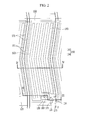
- FIG. 2 illustrates a layout view of a liquid crystal display according to an embodiment of the invention.
- FIG. 3 illustrates a cross-sectional view taken along line III-III of FIG. 2
- FIG. 4 illustrates a cross-sectional view taken along line IV-IV of FIG. 2 .
- the liquid crystal display according to this embodiment may include a lower panel 100 and an upper panel 200 facing each other, and a liquid crystal layer 3 between the two panels 100 and 200.
- a plurality of gate lines 121 may be formed on an insulation substrate 110.
- the gate lines 121 may transfer gate signals and may extend in a horizontal direction.
- Each gate line 121 may include a plurality of gate electrodes 124.
- a gate insulating layer 140 may be formed on the gate line 121.
- the gate insulating layer 140 may be made of or may include, e.g., an inorganic insulator such as silicon nitride (SiNx) or silicon oxide (SiOx).
- a plurality of semiconductors 150 may be formed on the gate insulating layer 140.
- the semiconductor 150 may include a protrusion 154 extending along the gate electrode 124.
- the semiconductor 150 may be disposed only on the gate electrode 124.
- a plurality of ohmic contacts 161, 163, and 165 may be formed on the semiconductor 150.
- the ohmic contacts 163 and 165 may address each other over the gate electrode 124 and may be disposed on the protrusion 154 to make a pair.
- the ohmic contacts 161, 163, and 165 may be made of a material, e.g., n + hydrogenated amorphous silicon (in which an n-type impurity such as phosphorus is doped at high concentration) or a silicide.
- the ohmic contacts 161, 163, and 165 may be omitted.
- Data conductors including a plurality of data lines 171 and a plurality of drain electrodes 175, may be positioned on the ohmic contacts 161, 163, and 165.
- the data lines 171 may transfer data signals and may extend in a vertical direction to cross the gate lines 121.
- Each data line 171 may include a plurality of source electrodes 173 that extend toward the gate electrode 124.
- the data line 171 may be periodically curved and may form an oblique angle with an extending direction of the gate line 121.
- the oblique angle between the data line 171 and the extending direction of the gate line 121 may be about 45° or more.
- the data line 171 may extend in a straight line.
- the drain electrode 175 may include a rod-shaped end portion that faces the source electrode 173, based on the gate electrode 124 and the other wide end portion.
- the gate electrode 124, the source electrode 173, and the drain electrode 175 may form a thin film transistor (TFT), which is a switching element, together with the semiconductor protrusion 154.
- TFT thin film transistor
- a semiconductor stripe 151 may have almost the same planar shape as the data line 171, the drain electrode 175, and the ohmic contacts 161 and 165 therebelow, except for the semiconductor protrusion 154 where the thin film transistor is positioned.
- a first passivation layer 180x may be positioned on the data conductors 171 and 175 and the exposed semiconductor protrusion 154.
- the first passivation layer 180x may be made of or may include, e.g., an organic insulating material, an inorganic insulating material, or the like.
- a plurality of color filters 230A, 230B, and 230C may be disposed on the first passivation layer 180x.
- Each of the color filters 230A, 230B, and 230C may uniquely display one of the primary colors, and an example of the primary colors may include three primary colors such as red, green, and blue, or yellow, cyan, magenta, and the like.
- the color filters may further include a color filter displaying a mixed color of the primary colors or white other than the primary colors.
- the color filters 230A, 230B, and 230C may be made of or may include organic materials.
- Each of the color filters 230A, 230B, and 230C may be elongated along the data line 171, and two color filters 230A and 230B, or 230B and 230C, which are adjacent to each other on a boundary of the data line 171, may be overlapped with each other.
- a plurality of common electrodes 131 may be disposed on the color filters 230A, 230B, and 230C.
- the common electrode 131 may be made of or may include a transparent conductive material such as ITO or IZO.
- the common electrode 131 (e.g., having a planar shape) may be formed on an entire surface of the insulation substrate 110 in a whole plate, and may have an opening 138 in a region corresponding to or overlying a periphery of the drain electrode 175.
- a second passivation layer 180y may be disposed on the common electrode 131.
- the second passivation layer 180y may be made of or may include an organic insulating material or an inorganic insulating material.
- a pixel electrode 191 may be formed on the second passivation layer 180y.
- the pixel electrode 191 may include a plurality of branch electrodes 193 (which may extend to be substantially parallel with each other and may be spaced apart from each other), and lower and upper horizontal portions 192 connecting upper and lower ends of the branch electrodes 193.
- the branch electrode 193 of the pixel electrode 191 may be curved along the data line 171.
- the data lines 171 and the branch electrode 193 of the pixel electrode 191 may extend in a straight line.
- the pixel electrode 191 may be made of or may include a transparent conductive material such as ITO or IZO.
- a plurality of contact holes 183 (exposing a part of the drain electrode 175) may be formed in the first passivation layer 180x, the color filter 230B, and the second passivation layer 180y, and the pixel electrode 191 may be electrically connected with the drain electrode 175 through the contact hole 183 to receive a data voltage.
- the contact hole 183 may be formed at a position corresponding to or aligned with the opening 138 in the common electrode 131.
- the pixel electrode 191 (receiving the data voltage) may generate an electric field in the liquid crystal layer 3 together with the common electrode 131 (receiving a common voltage).
- the branch electrodes 193 of the pixel electrode 191 may overlap with the common electrode 131 (which may have the planar shape).
- a first alignment layer 11 may be coated on an inner surface of the lower panel 100.
- the upper panel 200 may include an insulation substrate 210, and a light blocking member 220 on the insulation substrate 210.
- An overcoat 250 may be further formed on the light blocking member 220.
- a width of the light blocking member 220 may be larger than a width of the data line 171.
- a second alignment layer 21 may be coated on the overcoat 250.
- the first alignment layer 11 and the second alignment layer 21 may be vertical alignment layers for vertically aligning the liquid crystal molecules 31 inside the liquid crystal layer 3.
- the liquid crystal layer 3 between the lower panel 100 and the upper panel 200 may include liquid crystal molecules 31.
- the liquid crystal molecules 31 may be aligned so that long axes thereof are vertical or perpendicular to the surfaces of the two panels 100 and 200 when an electric field is not applied.
- the liquid crystal layer 3 may have positive dielectric anisotropy or may have negative dielectric anisotropy.
- the liquid crystal molecules of the liquid crystal layer 3 may be aligned to have pretilts in a predetermined direction, and the pretilt directions of the liquid crystal molecules may be changed according to dielectric anisotropy of the liquid crystal layer 3.
- the liquid crystal inside the liquid crystal display is manufactured in the in-plane switching mode
- the liquid crystal display when the liquid crystal display is processed in a curved shape, there may be a large change in behavior of the liquid crystal molecules due to misalignment of the upper insulation substrate 210 and the lower insulation substrate 110. As a result, light leakage may more frequently occur, as compared with the vertical field mode. Accordingly, an initial alignment of the liquid crystal molecules 31 (configuring the liquid crystal layer 3) when the liquid crystal display is in the off state may be formed in a vertical alignment to prevent the light leakage.
- a backlight unit (not illustrated) that generates light to supply the light to the two panels 100 and 200 may be further included at an outside of the substrate 110 of the lower panel 100.
- the pixel electrode 191 (to which the data voltage is applied) may generate an electric field in the liquid crystal layer 3 together with the common electrode 131 (receiving the common voltage) to determine or affect directions of the liquid crystal molecules of the liquid crystal layer 3 and may display the corresponding image.
- FIG. 5 illustrates a cross-sectional view of a liquid crystal display according to another embodiment of the invention, which is taken along line III-III of FIG. 2 .
- the liquid crystal display according to the embodiment illustrated in FIG. 5 may be substantially the same as the liquid crystal display according to the embodiment illustrated in FIG. 4 , except for a column spacer 80 and shapes of surfaces of color filters 230A, 230B, and 230C on a lower surface of the column spacer 80, and description for duplicated portions may be omitted.
- the liquid crystal display according to this embodiment may further include a column spacer 80 attached to or on a top of the light blocking member 220 (which is on the upper panel 200), unlike the liquid crystal display according to the embodiment illustrated in FIG. 4 .
- an overlapping portion of the color filters 230A and 230B below or underlying the column spacer 80 may have a flat shape, unlike protruding in a convex shape above the lower panel 100 in the liquid crystal display according to the embodiment illustrated in FIGS. 2 to 4 .
- upper or outer surfaces of the color filters the color filters 230A and 230B below or underlying the column spacer 80 may be flat and may be parallel or coplanar with one another.
- the column spacer 80 may support the upper panel 200 and the lower panel 100 to help maintain a predetermined cell gap between the upper panel 200 and the lower panel 100.
- respective constituent elements of the upper panel 200 and the lower panel 100 may correspond to different positions from initially formed positions because the liquid crystal display is bent in a curved shape.
- the upper panel 200 and the lower panel 100 may be bent in a curved shape, and the column spacer 80 attached to the upper panel 200 may correspond to or overlie a different position on the lower panel 100 from the initial corresponding or overlying position of the lower panel 100.
- the column spacer 80 may overlap with the color filters 230A, 230B, and 230C to be disposed over a convex portion above the lower panel 100 or a slope portion thereof.
- the initially formed cell gap and a cell gap after completing the curved liquid crystal display may be different from each other, and as a result, a luminance characteristic may deteriorate.
- the overlapping portions 230A and 230B or 230B and 230C of the color filters 230A, 230B, and 230C on the lower panel 100 facing the upper panel 200 may have a flat shape.
- a liquid crystal display according to yet another embodiment of the invention will be described in detail with reference to FIG. 6 .
- FIG. 6 illustrates a cross-sectional view of a liquid crystal display according to yet another embodiment of the invention, which is taken along line III-III of FIG. 2 .
- the liquid crystal display according to the embodiment illustrated in FIG. 6 is substantially the same as the liquid crystal display according to the embodiment illustrated in FIGS. 2 to 4 described above, except for a column spacer 80 and a shielding electrode 88 positioned on a lower surface of the column spacer 80, and description for duplicated portions may be omitted.
- a shielding electrode 88 may be disposed on the data line 171, unlike the liquid crystal display according to the embodiment illustrated in FIGS. 2 to 4 .
- the shielding electrode 88 may be positioned at both sides on the data line 171 along an edge of one pixel area.
- the shielding electrode 88 may include vertical portions on edges of the pixel area, and a horizontal portion connecting the vertical portions.
- the shielding electrodes need not be separated from each other for every pixel area, and may be connected to the entire adjacent pixels to be integrally formed.
- the vertical portions of the pixel electrode at the edges, and one or more horizontal portions connecting the vertical portions may exist for every pixel area, and the shielding electrodes may have a mesh form in all the pixels.
- the shielding electrode 88 may be made of or may include a transparent conductive material such as indium tin oxide (ITO) or indium zinc oxide (IZO), or a reflective metal such as aluminum, silver, chromium, or an alloy thereof.
- a transparent conductive material such as indium tin oxide (ITO) or indium zinc oxide (IZO)
- IZO indium zinc oxide
- a reflective metal such as aluminum, silver, chromium, or an alloy thereof.
- an additional electrode 270 may be disposed on the upper panel 200 to apply the same voltage as the additional electrode 270 of the upper panel 200 to the shielding electrode 88, and the same voltage may be applied between both electrodes.
- an electric field may not be generated between the shielding electrode 88 and the additional electrode 270 of the upper panel 200, and the liquid crystal layer positioned therebetween may not be aligned.
- the liquid crystal between the shielding electrode 88 and the additional electrode 270 of the upper panel 200 may be in a black state, and as a result, in the case where the liquid crystal expresses black, the liquid crystal itself may serve as the light blocking member 220. Accordingly, in the liquid crystal display according to this embodiment, the light blocking member 220 of the upper panel 200 may be omitted, unlike the liquid crystal display illustrated in FIGS. 2 to 4 .
- the liquid crystal display according to this embodiment may further include a third passivation layer 180z between the color filters 230A, 230B, and 230C and the common electrode 131.
- the third passivation layer 180z may be made of or may include an organic material, and may have a flat surface.
- the third passivation layer 180z may be between the adjacent pixels to help reduce a step due to the color filters 230A, 230B, and 230C, and may help the alignment layer 11 to be uniformly rubbed.
- the third passivation layer 180z may be an inorganic insulating layer, and may help prevent components of the color filters from being exposed outside, and in this case, the third passivation layer 180z may be formed at a lower temperature than the gate insulating layer 140 to help prevent the color filters 230A, 230B, and 230C therebelow from being deformed or discolored.
- the third passivation layer 180z may help reduce transmittance loss due to a difference in refractive index between the color filters (disposed therebelow) and the organic insulating layer.
- the liquid crystal display according to this embodiment may further include a column spacer 80 attached to or on a position corresponding to or overlying the shielding electrode 88 on the lower panel 100, unlike the liquid crystal display according to the embodiment illustrated in FIGS. 2 to 4 .
- respective constituent elements of the upper panel 200 and the lower panel 100 may correspond to different positions from initially formed positions because the liquid crystal display may be realigned or misaligned in a curved shape.
- the column spacer 80 (attached to the lower panel 100) may correspond to a different position from the initial corresponding position of the upper panel 200. Accordingly, the column spacer 80 may be disposed over the protrusion where the light blocking member 220 positioned on the upper panel 200 is positioned or positioned at the contact hole portion, and in this case, the initially formed cell gap and a cell gap after completing the curved liquid crystal display may be different from each other, and as a result, a luminance characteristic may deteriorate.
- the column spacer 80 attached to the lower panel 100 may correspond to a different position from the initial corresponding position of the upper panel 200. Accordingly, the light blocking member 220 may be positioned at an undesired position to cover the display area, and in this case, an aperture ratio may be decreased.
- the removing or omission of the light blocking member 220 formed on the upper panel 200 and the forming of the shielding electrode 88 on the lower panel may help prevent the luminance characteristic from deteriorating due to a change of the cell gap or reduction of the aperture ratio of the liquid crystal display by an effect of the light blocking member 220 and the column spacer 80, by removing or omitting the light blocking member 220 on the upper panel 200 facing the lower panel 100 in the case where the column spacer 80 is attached to the lower panel 100.
- FIG. 7 illustrates a layout view of a liquid crystal display device according to this embodiment.
- FIG. 8 illustrates a cross-sectional view taken along line IX-IX of FIG. 7
- FIG. 9 illustrates a cross-sectional view taken along line X-X of FIG. 7 .
- the liquid crystal display according to this embodiment may include a lower panel 100 and an upper panel 200 facing each other, and a liquid crystal layer 3 between the two display panels 100 and 200.
- a plurality of gate lines 121 may be positioned on an insulation substrate 110, and a gate insulating layer 140 may be formed on the gate line 121.
- a plurality of semiconductors 151 may be disposed on the gate insulating layer 140, and a plurality of ohmic contacts 161, 163, and 165 may be disposed on the semiconductors 151 and 154.
- a data conductor (including a plurality of data lines 171 and a plurality of drain electrodes 175) may be positioned on the ohmic contacts 161, 163, and 165.
- the data line 171 may be periodically curved, and may form an oblique angle with an extending direction of the gate line 121.
- the oblique angle between the data line 171 and the extending direction of the gate line 121 may be about 45° or more.
- the data line 171 may extend in a straight line.
- a first passivation layer 180x may be positioned on the data conductor 171 and 175 and the exposed semiconductor protrusion 154, and the first passivation layer 180x may be made of or may include an organic insulating material, an inorganic insulating material, or the like.
- a plurality of color filters 230A, 230B, and 230C may be disposed on the first passivation layer 180x.
- Each of the color filters 230A, 230B, and 230C may uniquely display one of the primary colors, and an example of the primary colors may include three primary colors such as red, green, and blue, or yellow, cyan, magenta, and the like.
- the color filters may further include a color filter displaying a mixed color of the primary colors or white other than the primary colors.
- the color filters 230A, 230B, and 230C may be made of or may include organic materials.
- Each of the color filters 230A, 230B, and 230C may be elongated along the data line 171, and two of the color filters 230A and 230B, or 230B and 230C (which are adjacent to each other on a boundary of the data line 171) may be overlapped with each other. For example, an edge or portion of one of the color filters may overlap an edge or portion of another of the color filters at the boundary of the data line 171.
- a plurality of pixel electrodes 191 may be disposed on the color filters 230A, 230B, and 230C.
- the pixel electrode 191 may have a planar shape that almost fills a region surrounded by the gate line 121 and the data line 171.
- An overall shape of the pixel electrode 191 may be generally a polygon having sides that are substantially parallel to the gate line 121 and the data line 171.
- the pixel electrode 191 may be made of or may include a transparent conductive material such as ITO or IZO.
- a plurality of contact holes 183 (exposing a part of the drain electrode 175) may be formed in the first passivation layer 180x and the color filter 230A, and the pixel electrode 191 may be electrically connected with the drain electrode 175 through the contact hole 183 to receive a data voltage.
- a second passivation layer 180y may be disposed on the color filters 230A, 230B, and 230C and the pixel electrode 191.
- the second passivation layer 180y may include an organic insulator or an inorganic insulator.
- a common electrode 131 may be disposed on the second passivation layer 180y.
- the common electrode 131 may be made of or may include a transparent conductive material such as ITO or IZO.
- the common electrodes 131 of adjacent pixels may be connected to each other.
- the common electrode 131 may include a plurality of branch electrodes 133 in each pixel area.
- the branch electrodes 133 may be substantially parallel to each other and may be curved along the data line 171. In an implementation, the data line 171 and the branch electrodes 133 of the pixel electrode 131 may extend in a straight line.
- the branch electrodes 133 of the common electrode 131 may overlap with or overlie the pixel electrode 191.
- the pixel electrode 191 (receiving the data voltage) may generate an electric field in the liquid crystal layer 3, together with the common electrode 131 (receiving the common voltage).
- the upper panel 200 may include an insulation substrate 210 and a light blocking member 220 on the insulation substrate 210.
- An overcoat 250 may be further formed on the light blocking member 220.
- a width of the light blocking member 220 may be larger than a width of the data line 171.
- a second alignment layer 21 may be coated on the overcoat 250.
- the first alignment layer 11 and the second alignment layer 21 may be vertical alignment layers for vertically aligning the liquid crystal molecules 31 inside the liquid crystal layer 3.
- the liquid crystal layer 3 between the lower panel 100 and the upper panel 200 may include liquid crystal molecules 31, and the liquid crystal molecules 31 may be aligned so that long axes thereof are vertical or perpendicular to the surfaces of the two panels 100 and 200 while an electric field is not applied.
- the liquid crystal layer 3 may have positive dielectric anisotropy or may have negative dielectric anisotropy.
- the liquid crystal molecules of the liquid crystal layer 3 may be aligned to have pretilts in a predetermined direction, and the pretilt directions of the liquid crystal molecules may be changed according to dielectric anisotropy of the liquid crystal layer 3.
- the liquid crystal inside the liquid crystal display is manufactured in the in-plane switching mode
- the liquid crystal display when the liquid crystal display is processed in a curved shape, there may be a large change in behavior of the liquid crystal molecules due to misalignment of the upper insulation substrate 210 and the lower insulation substrate 110, and as a result, light leakage may more frequently occur, as compared with the vertical field mode. Accordingly, an initial alignment of the liquid crystal molecules 31 (configuring the liquid crystal layer 3) when the liquid crystal display is in the off state may be formed in a vertical alignment to help prevent the light leakage.
- a backlight unit (not illustrated) that generates light to supply the light to the two panels 100 and 200 may be further included outside of the substrate 110 of the lower panel 100.
- the pixel electrode 191 to which the data voltage is applied may generate an electric field in the liquid crystal layer 3 together with the common electrode 131 (receiving the common voltage) to determine or affect directions of the liquid crystal molecules of the liquid crystal layer 3 and to display the corresponding image.
- a liquid crystal display according to yet another embodiment of the invention will be described in detail with reference to FIG. 10 .
- FIG. 10 illustrates a cross-sectional view of a liquid crystal display according to this embodiment.
- the liquid crystal display may include a lower panel 100 including a thin film transistor, an upper panel 200 facing the lower panel 100, and a liquid crystal layer 3 between the lower panel 100 and the upper panel 200.
- the common electrode 131 and the pixel electrode 191 may be formed on the lower panel 100, and the common electrode 131 and the pixel electrode 191 may be formed at various electrode distances in one pixel area. Further, the liquid crystal molecules 31 inside the liquid crystal layer 3 may be vertically aligned on the lower panel 100 and the upper panel 200, when the electric field is not applied.
- a plurality of gate lines may be formed on the insulation substrate 110 (made of transparent glass or plastic), and a plurality of gate electrodes (not illustrated), protruding upwardly and downwardly from each gate line, may be formed.
- a storage electrode (not illustrated), made of the same material as the gate line, may be further formed on the same layer as the gate line.
- a gate insulating layer 140 may be formed on the gate line.
- a semiconductor (not illustrated), an ohmic contact (not illustrated), a data line (not illustrated), source/drain electrodes (not illustrated), and the like may be formed, and a passivation layer 180 may be formed thereon.
- a plurality of common electrodes 131 and pixel electrodes 191 may be formed at various electrode distances on the passivation layer 180, and a first alignment layer 11 may be formed on the common electrode 131 and the pixel electrode 191.
- the upper panel 200 may include an insulation substrate 210 made of transparent glass or plastic.
- a plurality of color filters (not illustrated) may be formed on the insulation substrate 210, an overcoat 250 may be formed on the color filter, and a second alignment layer 21 may be formed on the overcoat 250.
- the first alignment layer 11 and the second alignment layer 21 may be vertical alignment layers. Accordingly, when the electric field is not formed in the liquid crystal display, the liquid crystal molecules 31 may be almost vertical to the surfaces of the upper panel 200 and the lower panel 100.
- a vertical field may be formed around the common electrode 131 and the pixel electrode 191, and the liquid crystal molecules 31 may be aligned in an in-plane switching mode in a direction of the electric field.
- FIG. 11(a) illustrates an image obtained by measuring light leakage in black of a curved liquid crystal display according to a Comparative Example and a curved liquid crystal display according to an embodiment of the invention
- FIG. 11(b) illustrates an image obtained by measuring uniformity of luminance on gray of a curved liquid crystal display according to a Comparative Example and a curved liquid crystal display according to the embodiment.
- FIGS. 11(a) and 11(b) in a curved liquid crystal display according to an embodiment of the invention, it may be seen that light leakage in black is reduced, and uniformity of luminance on gray is improved.
- FIG. 12(a) illustrates an image obtained by measuring a white driving state of a curved liquid crystal display according to a Comparative Example
- FIG. 12(b) illustrates an image obtained by measuring a white driving state of a curved liquid crystal display according to an embodiment of the invention.
- FIG. 14(a) illustrates an image showing a simulation result of light leakage of a curved liquid crystal display according to a Comparative Example
- FIG. 14(b) illustrates an image showing a simulation result of light leakage of a curved liquid crystal display according to an embodiment of the invention.
- the pixel electrode and the common electrode may be provided on one display panel with a switching element.
- an in-plane switching mode liquid crystal display in which the liquid crystal is driven by only an electric field of the lower electrode
- light leakage due to distortion of the liquid crystal molecules may occur.
- the embodiments may provide a curved liquid crystal display in which liquid crystal molecules are vertically aligned in an in-plane switching mode.
- the embodiments may provide a curved liquid crystal display that helps prevent light leakage in an in-plane switching mode by vertically aligning initial liquid crystal molecules while driving a liquid crystal by an electric field of only a lower electrode.
- the embodiments may provide a curved liquid crystal display having excellent display quality even if misalignment of an upper panel and a lower panel of the curved liquid crystal display were to occur.
- a curved liquid crystal display may have advantages of preventing light leakage of the curved liquid crystal display by vertically aligning initial liquid crystal molecules in an in-plane switching mode (in which a liquid crystal is driven by only an electric field of a lower electrode) and having excellent display quality, even in the case where misalignment of an upper panel and a lower panel of the curved liquid crystal display occurs.
Abstract
Description
- The invention relates to a curved liquid crystal display.
- A liquid crystal display, which is one type of flat panel display, may include two sheets of display panels with field generating electrodes (such as a pixel electrode, a common electrode, or the like) and a liquid crystal layer interposed therebetween. The liquid crystal display device may generate an electric field in the liquid crystal layer by applying voltage to the field generating electrodes, and may determine or affect a direction of liquid crystal molecules of the liquid crystal layer by the generated electric field, thus controlling polarization of incident light so as to display images. Transmittance of the liquid crystal display may be increased as the liquid crystal molecules are effectively controlled.
- The above information disclosed in this Background section is only for enhancement of understanding of the background of the invention and therefore it may contain information that does not form the prior art that is already known in this country to a person of ordinary skill in the art.
- The invention sets-out to provide a curved liquid crystal display.
- Accordingly, the invention provides a curved liquid crystal display including a first substrate having a curved shape; a plurality of gate lines and a plurality of data lines on the first substrate; a plurality of thin film transistors connected to the plurality of gate lines and the plurality of data lines; a plurality of color filters on the plurality of thin film transistors; a plurality of pixel electrodes and common electrodes on the plurality of color filters, the plurality of pixel electrodes and common electrodes overlapping with each other with a first insulating layer therebetween; a second substrate having a curved shape, the second substrate facing the first substrate; vertical alignment layers on inner sides of the first substrate and the second substrate; and a liquid crystal layer between the vertical alignment layers, wherein liquid crystal molecules of the liquid crystal layer are aligned to be vertical to surfaces of the first substrate and the second substrate when an electric field is not formed.
- The liquid crystal molecules may be aligned to be horizontal to the surfaces of the first substrate and the second substrate and in the direction of the electric field, when the electric field is formed in the liquid crystal layer.
- The common electrode may be on the plurality of color filters, the first insulating layer may be on the common electrode, and the plurality of pixel electrodes may be on the first insulating layer.
- The curved liquid crystal display may further include a light blocking member on the second substrate and at a position overlying a region where two adjacent color filters of the plurality of color filters overlap with each other.
- A width of the light blocking member may be the same as or larger than a width of the data line.
- The curved liquid crystal display may further include a column spacer attached to the light blocking member.
- A portion of the color filters where the plurality of color filters overlaps with each other may have a flat shape.
- The curved liquid crystal display may further include a shielding electrode on the first substrate, the shielding electrode being at a position overlying an interface between two adjacent color filters of the plurality of color filters and the data line; and an additional electrode on the second substrate.
- The curved liquid crystal display may further include a column spacer attached onto the shielding electrode.
- The plurality of pixel electrodes may be on the plurality of color filters, the first insulating layer may be on the pixel electrode, and the common electrode may be on the first insulating layer.
- The curved liquid crystal display may further include a light blocking member on the second substrate and at a position overlying a region where two adjacent color filters among the plurality of color filters overlap with each other.
- A width of the light blocking member may be the same as or larger than a width of the data line.
- The curved liquid crystal display may further include a column spacer attached onto the light blocking member.
- A portion of the color filters where the plurality of color filters may overlap with each other has a flat shape.
- The curved liquid crystal display may further include a light blocking member between two adjacent color filters among the plurality of color filters, the light blocking member being on the first substrate and at a position overlying the data line.
- The curved liquid crystal display may further include a column spacer attached onto the light blocking member.
- A further aspect of the invention provides a curved liquid crystal display including a first substrate having a curved shape; a plurality of common electrodes and a plurality of pixel electrodes on the first substrate, the plurality of common electrodes and plurality of pixel electrodes being alternately separated from each other and being on a same layer; a second substrate having a curved shape, the second substrate facing the first substrate; vertical alignment layers on inner sides of the first substrate and the second substrate; and a liquid crystal layer between the vertical alignment layers, wherein liquid crystal molecules of the liquid crystal layer are aligned to be vertical to surfaces of the first substrate and the second substrate when an electric field is not formed.
- The liquid crystal molecules may be aligned to be horizontal to the surfaces of the first substrate and the second substrate in the direction of the electric field, when the electric field is formed in the liquid crystal layer.
- At least some of the above and other features of the invention are set-out in the claims.
- Features of the invention will be made more apparent to those of skill in the art by describing embodiments thereof with reference to the attached drawings in which:
-
FIG. 1 illustrates a schematic diagram of a liquid crystal display according to an embodiment of the invention. -
FIG. 2 illustrates a layout view of the liquid crystal display according to the embodiment of the invention. -
FIG. 3 illustrates a cross-sectional view taken along line III-III ofFIG. 2 . -
FIG. 4 illustrates a cross-sectional view taken along line IV-IV ofFIG. 2 . -
FIG. 5 illustrates a cross-sectional view of a liquid crystal display according to another embodiment of the invention, which is taken along line III-III ofFIG. 2 . -
FIG. 6 illustrates a cross-sectional view of a liquid crystal display according to yet another embodiment of the invention, which is taken along line III-III ofFIG. 2 . -
FIG. 7 illustrates a layout view of a liquid crystal display device according to yet another embodiment of the invention. -
FIG. 8 illustrates a cross-sectional view taken along line IX-IX ofFIG. 7 . -
FIG. 9 illustrates a cross-sectional view taken along line X-X ofFIG. 7 . -
FIG. 10 illustrates a cross-sectional view of a liquid crystal display device according to yet another embodiment of the invention. -
FIG. 11 illustrates a diagram of a result of measuring light leakage in black and uniformity of luminance on gray in curved liquid crystal displays according to an embodiment of the invention and a Comparative Example. -
FIG. 12 illustrates a diagram of a result of measuring generation of spots in curved liquid crystal displays according to an embodiment of the invention and Comparative Example. -
FIG. 13 illustrates a diagram of a result of measuring changes in color coordinates for each position before and after forming a curved surface in a curved liquid crystal display according to an embodiment of the invention. -
FIG. 14 illustrates a diagram illustrating a result of measuring light leakage in a black state in curved liquid crystal displays according to an embodiment of the invention and Comparative Example. - Example embodiments of the invention will now be described more fully hereinafter with reference to the accompanying drawings; however, the invention may be embodied in different forms and should not be construed as limited to the embodiments set forth herein. Rather, these embodiments are provided so that this disclosure will be thorough, and will convey suitable implementations to those skilled in the art.
- In the drawing figures, the dimensions of layers and regions may be exaggerated for clarity of illustration. Like reference numerals refer to like elements throughout.
- It will be understood that when an element such as a layer, film, region, or substrate is referred to as being "on" another element, it can be directly on the other element or intervening elements may also be present. In contrast, when an element is referred to as being "directly on" another element, there are no intervening elements present.
- First, a liquid crystal display according to an embodiment of the invention will be described in detail with reference to
FIG. 1 . -
FIG. 1 illustrates a schematic diagram of a liquid crystal display according to an embodiment of the invention. - As illustrated in
FIG. 1 , the liquid crystal display according to this embodiment may include alower insulation substrate 110, a plurality ofcommon electrodes 131 andpixel electrodes 191 on thelower insulation substrate 110, anupper insulation substrate 210 facing thelower insulation substrate 110, and aliquid crystal layer 3 between theupper insulation substrate 210 and thelower insulation substrate 110. - The
liquid crystal layer 3 may be formed in an in-plane switching mode, which may be driven by only an electric field of thecommon electrode 131 and thepixel electrode 191 on thelower insulation substrate 210. -
FIG. 1(a) illustrates an off state of the liquid crystal display, andFIG. 1(b) illustrates an on state of the liquid crystal display. - As illustrated in
FIG. 1(a) , liquid crystal molecules 31 (configuring the liquid crystal layer 3) may be in a vertically aligned state when the liquid crystal display is in the off state. As illustrated inFIG. 1(b) , liquid crystal molecules 31 (configuring the liquid crystal layer 3) may be driven in an in-plane switching mode by the electric field of the plurality ofcommon electrodes 131 and pixel electrodes 191 (formed only on the lower insulation substrate 210) when the liquid crystal display is turned on. - After the liquid crystal inside the liquid crystal display is manufactured in a vertical field mode, when the liquid crystal display is processed in a curved shape, there may be no large change in behavior of the liquid crystal molecules due to misalignment of the
upper insulation substrate 210 and thelower insulation substrate 110. - However, in the case where the liquid crystal inside the liquid crystal display is manufactured in the in-plane switching mode, when the liquid crystal display is processed in a curved shape, there may be a large change in behavior of the liquid crystal molecules due to misalignment of the
upper insulation substrate 210 and thelower insulation substrate 110. As a result, light leakage may occur to a greater degree, as compared with the vertical field mode. Accordingly, an initial alignment of the liquid crystal molecules 31 (configuring the liquid crystal layer 3) when the liquid crystal display is in the off state may be formed in a vertical alignment to prevent the light leakage. - Further, when the liquid crystal display is in the on state, the liquid crystal display may be implemented in an existing in-plane switching mode. For example, according to an embodiment of the invention, in an off state, the initial alignment of the
liquid crystal molecules 31 of theliquid crystal layer 3 may be perpendicular to a tangent of thecurved substrate liquid crystal molecule 31 that is under the influence of the electric field may be aligned with the surface of thecurved substrate liquid crystal molecule 31 may be parallel with a tangent line of thecurved substrate - Next, a liquid crystal display according to an embodiment of the invention will be described in detail with reference to
FIGS. 2 to 4 . -
FIG. 2 illustrates a layout view of a liquid crystal display according to an embodiment of the invention.FIG. 3 illustrates a cross-sectional view taken along line III-III ofFIG. 2 , andFIG. 4 illustrates a cross-sectional view taken along line IV-IV ofFIG. 2 . - The liquid crystal display according to this embodiment may include a
lower panel 100 and anupper panel 200 facing each other, and aliquid crystal layer 3 between the twopanels - First, the
lower panel 100 will be described. - A plurality of
gate lines 121 may be formed on aninsulation substrate 110. - The gate lines 121 may transfer gate signals and may extend in a horizontal direction. Each
gate line 121 may include a plurality ofgate electrodes 124. - A
gate insulating layer 140 may be formed on thegate line 121. Thegate insulating layer 140 may be made of or may include, e.g., an inorganic insulator such as silicon nitride (SiNx) or silicon oxide (SiOx). - A plurality of
semiconductors 150 may be formed on thegate insulating layer 140. Thesemiconductor 150 may include aprotrusion 154 extending along thegate electrode 124. In an implementation, thesemiconductor 150 may be disposed only on thegate electrode 124. - A plurality of
ohmic contacts semiconductor 150. Theohmic contacts gate electrode 124 and may be disposed on theprotrusion 154 to make a pair. Theohmic contacts ohmic contacts - Data conductors, including a plurality of
data lines 171 and a plurality ofdrain electrodes 175, may be positioned on theohmic contacts - The data lines 171 may transfer data signals and may extend in a vertical direction to cross the gate lines 121. Each
data line 171 may include a plurality ofsource electrodes 173 that extend toward thegate electrode 124. Thedata line 171 may be periodically curved and may form an oblique angle with an extending direction of thegate line 121. The oblique angle between thedata line 171 and the extending direction of thegate line 121 may be about 45° or more. In an implementation, thedata line 171 may extend in a straight line. - The
drain electrode 175 may include a rod-shaped end portion that faces thesource electrode 173, based on thegate electrode 124 and the other wide end portion. - The
gate electrode 124, thesource electrode 173, and thedrain electrode 175 may form a thin film transistor (TFT), which is a switching element, together with thesemiconductor protrusion 154. Asemiconductor stripe 151 may have almost the same planar shape as thedata line 171, thedrain electrode 175, and theohmic contacts semiconductor protrusion 154 where the thin film transistor is positioned. - A
first passivation layer 180x may be positioned on thedata conductors semiconductor protrusion 154. Thefirst passivation layer 180x may be made of or may include, e.g., an organic insulating material, an inorganic insulating material, or the like. - A plurality of
color filters first passivation layer 180x. Each of thecolor filters color filters color filters data line 171, and twocolor filters data line 171, may be overlapped with each other. - A plurality of
common electrodes 131 may be disposed on thecolor filters common electrode 131 may be made of or may include a transparent conductive material such as ITO or IZO. The common electrode 131 (e.g., having a planar shape) may be formed on an entire surface of theinsulation substrate 110 in a whole plate, and may have anopening 138 in a region corresponding to or overlying a periphery of thedrain electrode 175. - A
second passivation layer 180y may be disposed on thecommon electrode 131. Thesecond passivation layer 180y may be made of or may include an organic insulating material or an inorganic insulating material. - A
pixel electrode 191 may be formed on thesecond passivation layer 180y. Thepixel electrode 191 may include a plurality of branch electrodes 193 (which may extend to be substantially parallel with each other and may be spaced apart from each other), and lower and upperhorizontal portions 192 connecting upper and lower ends of thebranch electrodes 193. Thebranch electrode 193 of thepixel electrode 191 may be curved along thedata line 171. In an implementation, thedata lines 171 and thebranch electrode 193 of thepixel electrode 191 may extend in a straight line. Thepixel electrode 191 may be made of or may include a transparent conductive material such as ITO or IZO. - A plurality of contact holes 183 (exposing a part of the drain electrode 175) may be formed in the
first passivation layer 180x, thecolor filter 230B, and thesecond passivation layer 180y, and thepixel electrode 191 may be electrically connected with thedrain electrode 175 through thecontact hole 183 to receive a data voltage. - The
contact hole 183 may be formed at a position corresponding to or aligned with theopening 138 in thecommon electrode 131. - The pixel electrode 191 (receiving the data voltage) may generate an electric field in the
liquid crystal layer 3 together with the common electrode 131 (receiving a common voltage). - The
branch electrodes 193 of thepixel electrode 191 may overlap with the common electrode 131 (which may have the planar shape). - A
first alignment layer 11 may be coated on an inner surface of thelower panel 100. - Next, the
upper panel 200 will be described. - The
upper panel 200 may include aninsulation substrate 210, and alight blocking member 220 on theinsulation substrate 210. Anovercoat 250 may be further formed on thelight blocking member 220. - A width of the
light blocking member 220 may be larger than a width of thedata line 171. - A
second alignment layer 21 may be coated on theovercoat 250. - The
first alignment layer 11 and thesecond alignment layer 21 may be vertical alignment layers for vertically aligning theliquid crystal molecules 31 inside theliquid crystal layer 3. - The
liquid crystal layer 3 between thelower panel 100 and theupper panel 200 may includeliquid crystal molecules 31. Theliquid crystal molecules 31 may be aligned so that long axes thereof are vertical or perpendicular to the surfaces of the twopanels - The
liquid crystal layer 3 may have positive dielectric anisotropy or may have negative dielectric anisotropy. The liquid crystal molecules of theliquid crystal layer 3 may be aligned to have pretilts in a predetermined direction, and the pretilt directions of the liquid crystal molecules may be changed according to dielectric anisotropy of theliquid crystal layer 3. - As noted above, after the liquid crystal inside the liquid crystal display is manufactured in a vertical field mode, when the liquid crystal display is processed in a curved shape, there may be no large change in behavior of the liquid crystal molecules due to misalignment of the
upper insulation substrate 210 and thelower insulation substrate 110. - In the case where the liquid crystal inside the liquid crystal display is manufactured in the in-plane switching mode, when the liquid crystal display is processed in a curved shape, there may be a large change in behavior of the liquid crystal molecules due to misalignment of the
upper insulation substrate 210 and thelower insulation substrate 110. As a result, light leakage may more frequently occur, as compared with the vertical field mode. Accordingly, an initial alignment of the liquid crystal molecules 31 (configuring the liquid crystal layer 3) when the liquid crystal display is in the off state may be formed in a vertical alignment to prevent the light leakage. - A backlight unit (not illustrated) that generates light to supply the light to the two
panels substrate 110 of thelower panel 100. - The pixel electrode 191 (to which the data voltage is applied) may generate an electric field in the
liquid crystal layer 3 together with the common electrode 131 (receiving the common voltage) to determine or affect directions of the liquid crystal molecules of theliquid crystal layer 3 and may display the corresponding image. - Next, a liquid crystal display according to another embodiment of the invention will be described in detail with reference to
FIG. 5 . -
FIG. 5 illustrates a cross-sectional view of a liquid crystal display according to another embodiment of the invention, which is taken along line III-III ofFIG. 2 . - The liquid crystal display according to the embodiment illustrated in
FIG. 5 may be substantially the same as the liquid crystal display according to the embodiment illustrated inFIG. 4 , except for acolumn spacer 80 and shapes of surfaces ofcolor filters column spacer 80, and description for duplicated portions may be omitted. - The liquid crystal display according to this embodiment may further include a
column spacer 80 attached to or on a top of the light blocking member 220 (which is on the upper panel 200), unlike the liquid crystal display according to the embodiment illustrated inFIG. 4 . - Further, an overlapping portion of the
color filters column spacer 80 may have a flat shape, unlike protruding in a convex shape above thelower panel 100 in the liquid crystal display according to the embodiment illustrated inFIGS. 2 to 4 . For example, upper or outer surfaces of the color filters thecolor filters column spacer 80 may be flat and may be parallel or coplanar with one another. - The
column spacer 80 may support theupper panel 200 and thelower panel 100 to help maintain a predetermined cell gap between theupper panel 200 and thelower panel 100. - When the curved liquid crystal display is manufactured, respective constituent elements of the
upper panel 200 and thelower panel 100 may correspond to different positions from initially formed positions because the liquid crystal display is bent in a curved shape. - The
upper panel 200 and thelower panel 100 may be bent in a curved shape, and thecolumn spacer 80 attached to theupper panel 200 may correspond to or overlie a different position on thelower panel 100 from the initial corresponding or overlying position of thelower panel 100. As a result, thecolumn spacer 80 may overlap with thecolor filters lower panel 100 or a slope portion thereof. In this case, the initially formed cell gap and a cell gap after completing the curved liquid crystal display may be different from each other, and as a result, a luminance characteristic may deteriorate. - In order to help prevent the deterioration of the luminance characteristic, in the case where the
column spacer 80 is attached to or on theupper panel 200, the overlappingportions color filters lower panel 100 facing theupper panel 200 may have a flat shape. - A liquid crystal display according to yet another embodiment of the invention will be described in detail with reference to
FIG. 6 . -
FIG. 6 illustrates a cross-sectional view of a liquid crystal display according to yet another embodiment of the invention, which is taken along line III-III ofFIG. 2 . - The liquid crystal display according to the embodiment illustrated in
FIG. 6 is substantially the same as the liquid crystal display according to the embodiment illustrated inFIGS. 2 to 4 described above, except for acolumn spacer 80 and a shieldingelectrode 88 positioned on a lower surface of thecolumn spacer 80, and description for duplicated portions may be omitted. - In the liquid crystal display according to this embodiment illustrated in
FIG. 6 , a shieldingelectrode 88 may be disposed on thedata line 171, unlike the liquid crystal display according to the embodiment illustrated inFIGS. 2 to 4 . The shieldingelectrode 88 may be positioned at both sides on thedata line 171 along an edge of one pixel area. The shieldingelectrode 88 may include vertical portions on edges of the pixel area, and a horizontal portion connecting the vertical portions. - The shielding electrodes need not be separated from each other for every pixel area, and may be connected to the entire adjacent pixels to be integrally formed. For example, the vertical portions of the pixel electrode at the edges, and one or more horizontal portions connecting the vertical portions, may exist for every pixel area, and the shielding electrodes may have a mesh form in all the pixels.
- The shielding
electrode 88 may be made of or may include a transparent conductive material such as indium tin oxide (ITO) or indium zinc oxide (IZO), or a reflective metal such as aluminum, silver, chromium, or an alloy thereof. - Further, an
additional electrode 270 may be disposed on theupper panel 200 to apply the same voltage as theadditional electrode 270 of theupper panel 200 to the shieldingelectrode 88, and the same voltage may be applied between both electrodes. As a result, an electric field may not be generated between the shieldingelectrode 88 and theadditional electrode 270 of theupper panel 200, and the liquid crystal layer positioned therebetween may not be aligned. In this case, the liquid crystal between the shieldingelectrode 88 and theadditional electrode 270 of theupper panel 200 may be in a black state, and as a result, in the case where the liquid crystal expresses black, the liquid crystal itself may serve as thelight blocking member 220. Accordingly, in the liquid crystal display according to this embodiment, thelight blocking member 220 of theupper panel 200 may be omitted, unlike the liquid crystal display illustrated inFIGS. 2 to 4 . - Further, the liquid crystal display according to this embodiment may further include a
third passivation layer 180z between thecolor filters common electrode 131. Thethird passivation layer 180z may be made of or may include an organic material, and may have a flat surface. Thethird passivation layer 180z may be between the adjacent pixels to help reduce a step due to thecolor filters alignment layer 11 to be uniformly rubbed. Further, thethird passivation layer 180z may be an inorganic insulating layer, and may help prevent components of the color filters from being exposed outside, and in this case, thethird passivation layer 180z may be formed at a lower temperature than thegate insulating layer 140 to help prevent thecolor filters third passivation layer 180z may help reduce transmittance loss due to a difference in refractive index between the color filters (disposed therebelow) and the organic insulating layer. - The liquid crystal display according to this embodiment may further include a
column spacer 80 attached to or on a position corresponding to or overlying the shieldingelectrode 88 on thelower panel 100, unlike the liquid crystal display according to the embodiment illustrated inFIGS. 2 to 4 . - When the curved liquid crystal display is manufactured, respective constituent elements of the
upper panel 200 and thelower panel 100 may correspond to different positions from initially formed positions because the liquid crystal display may be realigned or misaligned in a curved shape. - If the
light blocking member 220 is formed on theupper panel 200, and theupper panel 200 and thelower panel 100 are bent in a curved shape, the column spacer 80 (attached to the lower panel 100) may correspond to a different position from the initial corresponding position of theupper panel 200. Accordingly, thecolumn spacer 80 may be disposed over the protrusion where thelight blocking member 220 positioned on theupper panel 200 is positioned or positioned at the contact hole portion, and in this case, the initially formed cell gap and a cell gap after completing the curved liquid crystal display may be different from each other, and as a result, a luminance characteristic may deteriorate. - Further, if the
light blocking member 220 is formed on theupper panel 200, and theupper panel 200 and thelower panel 100 are bent in a curved shape, thecolumn spacer 80 attached to thelower panel 100 may correspond to a different position from the initial corresponding position of theupper panel 200. Accordingly, thelight blocking member 220 may be positioned at an undesired position to cover the display area, and in this case, an aperture ratio may be decreased. - The removing or omission of the
light blocking member 220 formed on theupper panel 200 and the forming of the shieldingelectrode 88 on the lower panel may help prevent the luminance characteristic from deteriorating due to a change of the cell gap or reduction of the aperture ratio of the liquid crystal display by an effect of thelight blocking member 220 and thecolumn spacer 80, by removing or omitting thelight blocking member 220 on theupper panel 200 facing thelower panel 100 in the case where thecolumn spacer 80 is attached to thelower panel 100. - Next, a liquid crystal display according to yet another embodiment of the invention will be described in detail with reference to
FIGS. 7 to 9 . -
FIG. 7 illustrates a layout view of a liquid crystal display device according to this embodiment.FIG. 8 illustrates a cross-sectional view taken along line IX-IX ofFIG. 7 , andFIG. 9 illustrates a cross-sectional view taken along line X-X ofFIG. 7 . - The liquid crystal display according to this embodiment may include a
lower panel 100 and anupper panel 200 facing each other, and aliquid crystal layer 3 between the twodisplay panels - First, the
lower panel 100 will be described. - A plurality of gate lines 121 (including a plurality of gate electrodes 124) may be positioned on an
insulation substrate 110, and agate insulating layer 140 may be formed on thegate line 121. A plurality of semiconductors 151 (including a plurality of protrusions 154) may be disposed on thegate insulating layer 140, and a plurality ofohmic contacts semiconductors data lines 171 and a plurality of drain electrodes 175) may be positioned on theohmic contacts data line 171 may be periodically curved, and may form an oblique angle with an extending direction of thegate line 121. The oblique angle between thedata line 171 and the extending direction of thegate line 121 may be about 45° or more. In an implementation, thedata line 171 may extend in a straight line. - A
first passivation layer 180x may be positioned on thedata conductor semiconductor protrusion 154, and thefirst passivation layer 180x may be made of or may include an organic insulating material, an inorganic insulating material, or the like. - A plurality of
color filters first passivation layer 180x. Each of thecolor filters color filters color filters data line 171, and two of thecolor filters data line 171. - A plurality of
pixel electrodes 191 may be disposed on thecolor filters pixel electrode 191 may have a planar shape that almost fills a region surrounded by thegate line 121 and thedata line 171. An overall shape of thepixel electrode 191 may be generally a polygon having sides that are substantially parallel to thegate line 121 and thedata line 171. Thepixel electrode 191 may be made of or may include a transparent conductive material such as ITO or IZO. - A plurality of contact holes 183 (exposing a part of the drain electrode 175) may be formed in the
first passivation layer 180x and thecolor filter 230A, and thepixel electrode 191 may be electrically connected with thedrain electrode 175 through thecontact hole 183 to receive a data voltage. - A
second passivation layer 180y may be disposed on thecolor filters pixel electrode 191. Thesecond passivation layer 180y may include an organic insulator or an inorganic insulator. - A
common electrode 131 may be disposed on thesecond passivation layer 180y. Thecommon electrode 131 may be made of or may include a transparent conductive material such as ITO or IZO. Thecommon electrodes 131 of adjacent pixels may be connected to each other. Thecommon electrode 131 may include a plurality ofbranch electrodes 133 in each pixel area. Thebranch electrodes 133 may be substantially parallel to each other and may be curved along thedata line 171. In an implementation, thedata line 171 and thebranch electrodes 133 of thepixel electrode 131 may extend in a straight line. - The
branch electrodes 133 of thecommon electrode 131 may overlap with or overlie thepixel electrode 191. - The pixel electrode 191 (receiving the data voltage) may generate an electric field in the
liquid crystal layer 3, together with the common electrode 131 (receiving the common voltage). - Next, the
upper panel 200 will be described. - The
upper panel 200 may include aninsulation substrate 210 and alight blocking member 220 on theinsulation substrate 210. Anovercoat 250 may be further formed on thelight blocking member 220. - A width of the
light blocking member 220 may be larger than a width of thedata line 171. - A
second alignment layer 21 may be coated on theovercoat 250. - The
first alignment layer 11 and thesecond alignment layer 21 may be vertical alignment layers for vertically aligning theliquid crystal molecules 31 inside theliquid crystal layer 3. - The
liquid crystal layer 3 between thelower panel 100 and theupper panel 200 may includeliquid crystal molecules 31, and theliquid crystal molecules 31 may be aligned so that long axes thereof are vertical or perpendicular to the surfaces of the twopanels - The
liquid crystal layer 3 may have positive dielectric anisotropy or may have negative dielectric anisotropy. The liquid crystal molecules of theliquid crystal layer 3 may be aligned to have pretilts in a predetermined direction, and the pretilt directions of the liquid crystal molecules may be changed according to dielectric anisotropy of theliquid crystal layer 3. - As noted above, after the liquid crystal inside the liquid crystal display is manufactured in a vertical field mode, when the liquid crystal display is processed in a curved shape, there may be no large change in behavior of the liquid crystal molecules due to misalignment of the
upper insulation substrate 210 and thelower insulation substrate 110. - In the case where the liquid crystal inside the liquid crystal display is manufactured in the in-plane switching mode, when the liquid crystal display is processed in a curved shape, there may be a large change in behavior of the liquid crystal molecules due to misalignment of the
upper insulation substrate 210 and thelower insulation substrate 110, and as a result, light leakage may more frequently occur, as compared with the vertical field mode. Accordingly, an initial alignment of the liquid crystal molecules 31 (configuring the liquid crystal layer 3) when the liquid crystal display is in the off state may be formed in a vertical alignment to help prevent the light leakage. - A backlight unit (not illustrated) that generates light to supply the light to the two
panels substrate 110 of thelower panel 100. - The
pixel electrode 191 to which the data voltage is applied may generate an electric field in theliquid crystal layer 3 together with the common electrode 131 (receiving the common voltage) to determine or affect directions of the liquid crystal molecules of theliquid crystal layer 3 and to display the corresponding image. - A liquid crystal display according to yet another embodiment of the invention will be described in detail with reference to
FIG. 10 . -
FIG. 10 illustrates a cross-sectional view of a liquid crystal display according to this embodiment. - Referring to
FIG. 10 , the liquid crystal display according to this embodiment of the invention may include alower panel 100 including a thin film transistor, anupper panel 200 facing thelower panel 100, and aliquid crystal layer 3 between thelower panel 100 and theupper panel 200. - The
common electrode 131 and the pixel electrode 191 (for forming the electric field) may be formed on thelower panel 100, and thecommon electrode 131 and thepixel electrode 191 may be formed at various electrode distances in one pixel area. Further, theliquid crystal molecules 31 inside theliquid crystal layer 3 may be vertically aligned on thelower panel 100 and theupper panel 200, when the electric field is not applied. - A plurality of gate lines (not illustrated) may be formed on the insulation substrate 110 (made of transparent glass or plastic), and a plurality of gate electrodes (not illustrated), protruding upwardly and downwardly from each gate line, may be formed. A storage electrode (not illustrated), made of the same material as the gate line, may be further formed on the same layer as the gate line.
- A
gate insulating layer 140 may be formed on the gate line. - On the
gate insulating layer 140, a semiconductor (not illustrated), an ohmic contact (not illustrated), a data line (not illustrated), source/drain electrodes (not illustrated), and the like may be formed, and apassivation layer 180 may be formed thereon. - A plurality of
common electrodes 131 andpixel electrodes 191 may be formed at various electrode distances on thepassivation layer 180, and afirst alignment layer 11 may be formed on thecommon electrode 131 and thepixel electrode 191. - The
upper panel 200 may include aninsulation substrate 210 made of transparent glass or plastic. A plurality of color filters (not illustrated) may be formed on theinsulation substrate 210, anovercoat 250 may be formed on the color filter, and asecond alignment layer 21 may be formed on theovercoat 250. - Here, the
first alignment layer 11 and thesecond alignment layer 21 may be vertical alignment layers. Accordingly, when the electric field is not formed in the liquid crystal display, theliquid crystal molecules 31 may be almost vertical to the surfaces of theupper panel 200 and thelower panel 100. - Further, when the electric field is formed in the liquid crystal display, a vertical field may be formed around the
common electrode 131 and thepixel electrode 191, and theliquid crystal molecules 31 may be aligned in an in-plane switching mode in a direction of the electric field. - In order to observe display quality of a curved liquid crystal display according to the invention, light leakage in black and uniformity of luminance on gray were measured. The result is illustrated in
FIG. 11 . -
FIG. 11(a) illustrates an image obtained by measuring light leakage in black of a curved liquid crystal display according to a Comparative Example and a curved liquid crystal display according to an embodiment of the invention, andFIG. 11(b) illustrates an image obtained by measuring uniformity of luminance on gray of a curved liquid crystal display according to a Comparative Example and a curved liquid crystal display according to the embodiment. - As illustrated in
FIGS. 11(a) and 11(b) , in a curved liquid crystal display according to an embodiment of the invention, it may be seen that light leakage in black is reduced, and uniformity of luminance on gray is improved. - In order to observe the display quality of a curved liquid crystal display according to the invention, generation of spots of display devices were measured. The result is illustrated in
FIG. 12 . -
FIG. 12(a) illustrates an image obtained by measuring a white driving state of a curved liquid crystal display according to a Comparative Example, andFIG. 12(b) illustrates an image obtained by measuring a white driving state of a curved liquid crystal display according to an embodiment of the invention. - As illustrated in
FIGS. 12(a) and 12(b) , in the case of the curved liquid crystal display according to the Comparative Example, a yellowish phenomenon was observed at left and right sides of the display device, while in the case of the curved liquid crystal display according to the embodiment, the yellowish phenomenon was completely improved. - Further, in order to observe generation of spots of a curved liquid crystal display according toinvention, changes in color coordinates for each position before and after forming the curved shape of the curved liquid crystal display according to an embodiment of the invention were measured, and the result is illustrated in
FIG. 13 . - As illustrated in
FIG. 13 , it may be seen that there was little change in color coordinate for each position before and after forming the curved shape of the curved liquid crystal display, and as a result, it may be seen that a spot phenomenon is improved. - The light leakage in the black state of a curved liquid crystal display according to the invention was measured, and the result is illustrated in
FIG. 14 . -
FIG. 14(a) illustrates an image showing a simulation result of light leakage of a curved liquid crystal display according to a Comparative Example, andFIG. 14(b) illustrates an image showing a simulation result of light leakage of a curved liquid crystal display according to an embodiment of the invention. - As illustrated in
FIGS. 14(a) and 14(b) , in the curved liquid crystal display according to the embodiment, it may be seen that light leakage was significantly improved, as compared with the curved liquid crystal display according to the Comparative Example. - By way of summation and review, in the liquid crystal display, the pixel electrode and the common electrode (generating the electric field in the liquid crystal layer) may be provided on one display panel with a switching element. In the case where an in-plane switching mode liquid crystal display (in which the liquid crystal is driven by only an electric field of the lower electrode) is manufactured in a curved shape, light leakage due to distortion of the liquid crystal molecules may occur.
- The embodiments may provide a curved liquid crystal display in which liquid crystal molecules are vertically aligned in an in-plane switching mode.
- The embodiments may provide a curved liquid crystal display that helps prevent light leakage in an in-plane switching mode by vertically aligning initial liquid crystal molecules while driving a liquid crystal by an electric field of only a lower electrode.
- The embodiments may provide a curved liquid crystal display having excellent display quality even if misalignment of an upper panel and a lower panel of the curved liquid crystal display were to occur.
- As described above, a curved liquid crystal display according to an embodiment of the invention may have advantages of preventing light leakage of the curved liquid crystal display by vertically aligning initial liquid crystal molecules in an in-plane switching mode (in which a liquid crystal is driven by only an electric field of a lower electrode) and having excellent display quality, even in the case where misalignment of an upper panel and a lower panel of the curved liquid crystal display occurs.
- Example embodiments of the invention have been disclosed herein, and although specific terms are employed, they are used and are to be interpreted in a generic and descriptive sense only and not for purpose of limitation. In some instances, as would be apparent to one of ordinary skill in the art as of the filing of the present application, features, characteristics, and/or elements described in connection with a particular embodiment may be used singly or in combination with features, characteristics, and/or elements described in connection with other embodiments unless otherwise specifically indicated. Accordingly, it will be understood by those of skill in the art that various changes in form and details may be made without departing from the scope of the present invention as set forth in the following claims.
Claims (11)
- A curved liquid crystal display, comprising:a first substrate having a curved shape;a plurality of gate lines and a plurality of data lines on the first substrate;a plurality of thin film transistors connected to the plurality of gate lines and the plurality of data lines;a plurality of color filters on the plurality of thin film transistors;a plurality of pixel electrodes and common electrodes on the plurality of color filters, the plurality of pixel electrodes and common electrodes overlapping with each other with a first insulating layer therebetween;a second substrate having a curved shape, the second substrate facing the first substrate;vertical alignment layers on inner sides of the first substrate and the second substrate; anda liquid crystal layer between the vertical alignment layers,wherein liquid crystal molecules of the liquid crystal layer are aligned to be perpendicular to surfaces of the first substrate and the second substrate when an electric field is not formed in the liquid crystal layer.
- A curved liquid crystal display as claimed in claim 1, wherein the liquid crystal molecules are aligned with the surfaces of the first substrate and the second substrate and in the direction of the electric field, when the electric field is formed in the liquid crystal layer.
- A curved liquid crystal display as claimed in claim 1 or 2, wherein:the common electrode is on the plurality of color filters,the first insulating layer is on the common electrode, andthe plurality of pixel electrodes is on the first insulating layer.
- A curved liquid crystal display as claimed in claim 1 or 2, wherein:the plurality of pixel electrodes is on the plurality of color filters,the first insulating layer is on the pixel electrode, andthe common electrode is on the first insulating layer.
- A curved liquid crystal display as claimed in any preceding claim, further comprising a light blocking member on the second substrate and at a position overlying a region where two adjacent color filters of the plurality of color filters overlap with each other.
- A curved liquid crystal display as claimed in claim 5, wherein a width of the light blocking member is the same as or larger than a width of the data line.
- A curved liquid crystal display as claimed in claim 5 or 6, further comprising a column spacer attached to the light blocking member.
- A curved liquid crystal display as claimed in claim 7, wherein a portion of the color filters where the plurality of color filters overlaps with the column spacer has a flat shape.
- A curved liquid crystal display as claimed in claim 3 or 4, further comprising:a shielding electrode on the first substrate, the shielding electrode being at a position overlying an interface between two adjacent color filters of the plurality of color filters and the data line; andan additional electrode on the second substrate.
- A curved liquid crystal display as claimed in claim 9, further comprising a column spacer attached onto the shielding electrode.
- A curved liquid crystal display as claimed in claim 4 or any claim dependent upon claim 4, further comprising a light blocking member between two adjacent color filters among the plurality of color filters, the light blocking member being on the first substrate and at a position overlying the data line.
Applications Claiming Priority (1)
| Application Number | Priority Date | Filing Date | Title |
|---|---|---|---|
| KR1020130167557A KR102135792B1 (en) | 2013-12-30 | 2013-12-30 | Curved liquid crystal display |
Publications (2)
| Publication Number | Publication Date |
|---|---|
| EP2889681A1 true EP2889681A1 (en) | 2015-07-01 |
| EP2889681B1 EP2889681B1 (en) | 2018-11-07 |
Family
ID=52134049
Family Applications (1)
| Application Number | Title | Priority Date | Filing Date |
|---|---|---|---|
| EP14200206.2A Not-in-force EP2889681B1 (en) | 2013-12-30 | 2014-12-23 | Curved liquid crystal display |
Country Status (4)
| Country | Link |
|---|---|
| US (2) | US9575377B2 (en) |
| EP (1) | EP2889681B1 (en) |
| KR (1) | KR102135792B1 (en) |
| CN (1) | CN104749839B (en) |
Families Citing this family (16)
| Publication number | Priority date | Publication date | Assignee | Title |
|---|---|---|---|---|
| CN103941453A (en) * | 2014-04-09 | 2014-07-23 | 合肥京东方光电科技有限公司 | Array substrate, display panel and display device |
| KR102228269B1 (en) | 2014-07-09 | 2021-03-17 | 삼성디스플레이 주식회사 | Display substrate and method of manufacturing the same |
| US9733526B2 (en) * | 2014-10-30 | 2017-08-15 | Shenzhen China Star Optoelectronics Technology Co., Ltd. | Curved display panel and curved display apparatus |
| KR102257106B1 (en) * | 2015-01-06 | 2021-05-27 | 삼성디스플레이 주식회사 | Liquid crystal display |
| JP2016157072A (en) * | 2015-02-26 | 2016-09-01 | 株式会社ジャパンディスプレイ | Display |
| KR20170001848A (en) | 2015-06-26 | 2017-01-05 | 삼성디스플레이 주식회사 | Liquid crystal display |
| KR102416574B1 (en) * | 2015-08-18 | 2022-07-08 | 삼성디스플레이 주식회사 | Curved liquid crystal display and method for manufacturing the same |
| CN105093653B (en) * | 2015-08-26 | 2018-05-29 | 深圳市华星光电技术有限公司 | A kind of color membrane substrates and curved-surface display device |
| CN105116657A (en) * | 2015-09-23 | 2015-12-02 | 深圳市华星光电技术有限公司 | Array substrate and liquid crystal display panel |
| KR102552594B1 (en) * | 2015-12-31 | 2023-07-05 | 엘지디스플레이 주식회사 | Liquid crystal display device |
| KR102554120B1 (en) * | 2016-03-24 | 2023-07-12 | 티씨엘 차이나 스타 옵토일렉트로닉스 테크놀로지 컴퍼니 리미티드 | Liquid crystal display |
| CN105807524B (en) | 2016-05-30 | 2019-04-16 | 京东方科技集团股份有限公司 | Array substrate, display panel and display device |
| JP2017215411A (en) * | 2016-05-31 | 2017-12-07 | パナソニック液晶ディスプレイ株式会社 | Liquid crystal display device |
| CN108878498B (en) * | 2018-07-03 | 2021-11-23 | 京东方科技集团股份有限公司 | Color film substrate, preparation method thereof and display panel |
| CN109634014A (en) | 2019-02-22 | 2019-04-16 | 鄂尔多斯市源盛光电有限责任公司 | A kind of display base plate and preparation method thereof, display panel, display device |
| CN113179654B (en) * | 2019-11-25 | 2023-04-11 | 京东方科技集团股份有限公司 | Array substrate, light control panel and display device |
Citations (5)
| Publication number | Priority date | Publication date | Assignee | Title |
|---|---|---|---|---|
| US6177973B1 (en) * | 1997-12-08 | 2001-01-23 | Hyundai Electronics Industries Co., Ltd. | Vertical alignment mode liquid crystal display having enhanced response time |
| US20110001910A1 (en) * | 2009-07-06 | 2011-01-06 | Hitachi Displays, Ltd. | Liquid crystal display device |
| JP2012242804A (en) * | 2011-05-24 | 2012-12-10 | Konica Minolta Advanced Layers Inc | Liquid crystal display device |
| JP2013050535A (en) * | 2011-08-30 | 2013-03-14 | Mitsubishi Electric Corp | Liquid crystal display device |
| US20130300996A1 (en) * | 2010-09-28 | 2013-11-14 | Dic Corporation | Novel liquid crystal display device and useful liquid crystal composition |
Family Cites Families (20)
| Publication number | Priority date | Publication date | Assignee | Title |
|---|---|---|---|---|
| KR100945579B1 (en) * | 2003-03-17 | 2010-03-08 | 삼성전자주식회사 | Panel for display device and method for manufacturing the panel and liquid crystal display including the panel |
| KR20050001945A (en) * | 2003-06-28 | 2005-01-07 | 삼성전자주식회사 | Liquid crystal display apparatus |
| KR101133754B1 (en) | 2004-08-19 | 2012-04-09 | 삼성전자주식회사 | Liquid crystal display device |
| KR101230304B1 (en) * | 2005-09-07 | 2013-02-06 | 삼성디스플레이 주식회사 | Liquid crystal display |
| KR101240647B1 (en) * | 2005-10-13 | 2013-03-08 | 삼성디스플레이 주식회사 | Liquid crystal display |
| KR101318247B1 (en) | 2007-02-26 | 2013-10-16 | 엘지디스플레이 주식회사 | Liquid crystal display device and method for manufacturing of the same |
| KR101286527B1 (en) * | 2007-04-16 | 2013-07-23 | 엘지디스플레이 주식회사 | Liquid Crystal Display Panel And Method for Fabricating Thereof |
| KR101421627B1 (en) | 2007-10-09 | 2014-07-24 | 삼성디스플레이 주식회사 | Display apparatus and method of driving the same |
| JP5322427B2 (en) * | 2007-12-19 | 2013-10-23 | 三菱電機株式会社 | Liquid crystal display |
| CN101216635B (en) * | 2008-01-17 | 2010-09-01 | 友达光电股份有限公司 | LCD device, photoelectric device and process for production thereof |
| KR101448001B1 (en) * | 2008-01-29 | 2014-10-13 | 삼성디스플레이 주식회사 | Liquid crystal display |
| WO2010137235A1 (en) * | 2009-05-29 | 2010-12-02 | シャープ株式会社 | Liquid crystal panel, method for manufacturing same, and liquid crystal display device |
| JP5621625B2 (en) * | 2011-01-28 | 2014-11-12 | コニカミノルタ株式会社 | Liquid crystal display |
| WO2013001984A1 (en) * | 2011-06-27 | 2013-01-03 | シャープ株式会社 | Liquid crystal display panel and liquid crystal display device |
| KR101939782B1 (en) * | 2011-09-07 | 2019-01-18 | 삼성디스플레이 주식회사 | Liquid crystal display device |
| KR101809657B1 (en) * | 2011-09-22 | 2017-12-18 | 삼성디스플레이 주식회사 | Liquid crystal display and manufacturing method thereof |
| KR20130032743A (en) * | 2011-09-23 | 2013-04-02 | 삼성디스플레이 주식회사 | Liquid crystal display |
| CN102707474B (en) * | 2012-05-11 | 2013-07-24 | 京东方科技集团股份有限公司 | Bending liquid crystal display screen and manufacturing method and manufacturing device of bending liquid crystal display |
| KR101319543B1 (en) * | 2012-05-17 | 2013-10-21 | 삼성디스플레이 주식회사 | Curved dispaly apparatus and multi display apparatus including the same |
| KR20140091100A (en) | 2012-12-26 | 2014-07-21 | 삼성디스플레이 주식회사 | Curved liquid crystal display device |
-
2013
- 2013-12-30 KR KR1020130167557A patent/KR102135792B1/en active IP Right Grant
-
2014
- 2014-09-26 US US14/498,430 patent/US9575377B2/en active Active
- 2014-12-09 CN CN201410747755.8A patent/CN104749839B/en not_active Expired - Fee Related
- 2014-12-23 EP EP14200206.2A patent/EP2889681B1/en not_active Not-in-force
-
2017
- 2017-02-16 US US15/434,297 patent/US10108055B2/en active Active
Patent Citations (5)
| Publication number | Priority date | Publication date | Assignee | Title |
|---|---|---|---|---|
| US6177973B1 (en) * | 1997-12-08 | 2001-01-23 | Hyundai Electronics Industries Co., Ltd. | Vertical alignment mode liquid crystal display having enhanced response time |
| US20110001910A1 (en) * | 2009-07-06 | 2011-01-06 | Hitachi Displays, Ltd. | Liquid crystal display device |
| US20130300996A1 (en) * | 2010-09-28 | 2013-11-14 | Dic Corporation | Novel liquid crystal display device and useful liquid crystal composition |
| JP2012242804A (en) * | 2011-05-24 | 2012-12-10 | Konica Minolta Advanced Layers Inc | Liquid crystal display device |
| JP2013050535A (en) * | 2011-08-30 | 2013-03-14 | Mitsubishi Electric Corp | Liquid crystal display device |
Also Published As
| Publication number | Publication date |
|---|---|
| US9575377B2 (en) | 2017-02-21 |
| KR20150080147A (en) | 2015-07-09 |
| US10108055B2 (en) | 2018-10-23 |
| KR102135792B1 (en) | 2020-07-21 |
| US20150185565A1 (en) | 2015-07-02 |
| US20170160605A1 (en) | 2017-06-08 |
| EP2889681B1 (en) | 2018-11-07 |
| CN104749839B (en) | 2019-08-16 |
| CN104749839A (en) | 2015-07-01 |
Similar Documents
| Publication | Publication Date | Title |
|---|---|---|
| US10108055B2 (en) | Curved liquid crystal display | |
| US9715149B2 (en) | Liquid crystal display comprising a first electrode having a plurality of branch electrodes and a wing connected to an end of a branch electrode | |
| US10558095B2 (en) | Liquid crystal display with reduced color mixing | |
| US7636144B2 (en) | Liquid crystal display device and method of manufacturing the same | |
| US8390753B2 (en) | Thin film transistor array panel and liquid crystal display having the same | |
| EP2573617A1 (en) | Active matrix liquid crystal display | |
| KR101309779B1 (en) | Liquid crystal display | |
| US20150022766A1 (en) | Liquid crystal display | |
| US9664965B2 (en) | Liquid crystal display device with a shielding electrode | |
| US8576365B2 (en) | Display panel | |
| US20060066781A1 (en) | Color filter panel, and liquid crystal display including color filter panel | |
| US9904133B2 (en) | Liquid crystal display | |
| US20130286314A1 (en) | Display element | |
| US20130321736A1 (en) | Liquid crystal display | |
| KR101046923B1 (en) | Thin film transistor array panel and liquid crystal display including the same | |
| KR20160095700A (en) | Liquid crystal display | |
| CN107219666B (en) | Color filter array panel and display device including the same | |
| US10649251B2 (en) | Curved liquid crystal display device and method of manufacturing the same | |
| JP4441507B2 (en) | Liquid crystal display | |
| US11003031B2 (en) | Display apparatus | |
| US8994903B2 (en) | Liquid crystal display |
Legal Events
| Date | Code | Title | Description |
|---|---|---|---|
| PUAI | Public reference made under article 153(3) epc to a published international application that has entered the european phase |
Free format text: ORIGINAL CODE: 0009012 |
|
| 17P | Request for examination filed |
Effective date: 20141223 |
|
| AK | Designated contracting states |
Kind code of ref document: A1 Designated state(s): AL AT BE BG CH CY CZ DE DK EE ES FI FR GB GR HR HU IE IS IT LI LT LU LV MC MK MT NL NO PL PT RO RS SE SI SK SM TR |
|
| AX | Request for extension of the european patent |
Extension state: BA ME |
|
| RAP1 | Party data changed (applicant data changed or rights of an application transferred) |
Owner name: SAMSUNG DISPLAY CO., LTD. |
|
| R17P | Request for examination filed (corrected) |
Effective date: 20151224 |
|
| RBV | Designated contracting states (corrected) |
Designated state(s): AL AT BE BG CH CY CZ DE DK EE ES FI FR GB GR HR HU IE IS IT LI LT LU LV MC MK MT NL NO PL PT RO RS SE SI SK SM TR |
|
| GRAP | Despatch of communication of intention to grant a patent |
Free format text: ORIGINAL CODE: EPIDOSNIGR1 |
|
| RIC1 | Information provided on ipc code assigned before grant |
Ipc: G02F 1/1335 20060101ALI20180416BHEP Ipc: G02F 1/1339 20060101ALN20180416BHEP Ipc: G02F 1/1362 20060101ALI20180416BHEP Ipc: G02F 1/1343 20060101AFI20180416BHEP |
|
| RIC1 | Information provided on ipc code assigned before grant |
Ipc: G02F 1/1343 20060101AFI20180504BHEP Ipc: G02F 1/1335 20060101ALI20180504BHEP Ipc: G02F 1/1339 20060101ALN20180504BHEP Ipc: G02F 1/1362 20060101ALI20180504BHEP |
|
| INTG | Intention to grant announced |
Effective date: 20180523 |
|
| GRAS | Grant fee paid |
Free format text: ORIGINAL CODE: EPIDOSNIGR3 |
|
| GRAA | (expected) grant |
Free format text: ORIGINAL CODE: 0009210 |
|
| AK | Designated contracting states |
Kind code of ref document: B1 Designated state(s): AL AT BE BG CH CY CZ DE DK EE ES FI FR GB GR HR HU IE IS IT LI LT LU LV MC MK MT NL NO PL PT RO RS SE SI SK SM TR |
|
| REG | Reference to a national code |
Ref country code: GB Ref legal event code: FG4D |
|
| REG | Reference to a national code |
Ref country code: AT Ref legal event code: REF Ref document number: 1062808 Country of ref document: AT Kind code of ref document: T Effective date: 20181115 Ref country code: CH Ref legal event code: EP |
|
| REG | Reference to a national code |
Ref country code: IE Ref legal event code: FG4D |
|
| REG | Reference to a national code |
Ref country code: DE Ref legal event code: R096 Ref document number: 602014035506 Country of ref document: DE |
|
| REG | Reference to a national code |
Ref country code: NL Ref legal event code: FP |
|
| REG | Reference to a national code |
Ref country code: LT Ref legal event code: MG4D |
|
| REG | Reference to a national code |
Ref country code: AT Ref legal event code: MK05 Ref document number: 1062808 Country of ref document: AT Kind code of ref document: T Effective date: 20181107 |
|
| PG25 | Lapsed in a contracting state [announced via postgrant information from national office to epo] |
Ref country code: AT Free format text: LAPSE BECAUSE OF FAILURE TO SUBMIT A TRANSLATION OF THE DESCRIPTION OR TO PAY THE FEE WITHIN THE PRESCRIBED TIME-LIMIT Effective date: 20181107 Ref country code: IS Free format text: LAPSE BECAUSE OF FAILURE TO SUBMIT A TRANSLATION OF THE DESCRIPTION OR TO PAY THE FEE WITHIN THE PRESCRIBED TIME-LIMIT Effective date: 20190307 Ref country code: LT Free format text: LAPSE BECAUSE OF FAILURE TO SUBMIT A TRANSLATION OF THE DESCRIPTION OR TO PAY THE FEE WITHIN THE PRESCRIBED TIME-LIMIT Effective date: 20181107 Ref country code: FI Free format text: LAPSE BECAUSE OF FAILURE TO SUBMIT A TRANSLATION OF THE DESCRIPTION OR TO PAY THE FEE WITHIN THE PRESCRIBED TIME-LIMIT Effective date: 20181107 Ref country code: BG Free format text: LAPSE BECAUSE OF FAILURE TO SUBMIT A TRANSLATION OF THE DESCRIPTION OR TO PAY THE FEE WITHIN THE PRESCRIBED TIME-LIMIT Effective date: 20190207 Ref country code: NO Free format text: LAPSE BECAUSE OF FAILURE TO SUBMIT A TRANSLATION OF THE DESCRIPTION OR TO PAY THE FEE WITHIN THE PRESCRIBED TIME-LIMIT Effective date: 20190207 Ref country code: HR Free format text: LAPSE BECAUSE OF FAILURE TO SUBMIT A TRANSLATION OF THE DESCRIPTION OR TO PAY THE FEE WITHIN THE PRESCRIBED TIME-LIMIT Effective date: 20181107 Ref country code: LV Free format text: LAPSE BECAUSE OF FAILURE TO SUBMIT A TRANSLATION OF THE DESCRIPTION OR TO PAY THE FEE WITHIN THE PRESCRIBED TIME-LIMIT Effective date: 20181107 Ref country code: ES Free format text: LAPSE BECAUSE OF FAILURE TO SUBMIT A TRANSLATION OF THE DESCRIPTION OR TO PAY THE FEE WITHIN THE PRESCRIBED TIME-LIMIT Effective date: 20181107 |
|
| PG25 | Lapsed in a contracting state [announced via postgrant information from national office to epo] |
Ref country code: AL Free format text: LAPSE BECAUSE OF FAILURE TO SUBMIT A TRANSLATION OF THE DESCRIPTION OR TO PAY THE FEE WITHIN THE PRESCRIBED TIME-LIMIT Effective date: 20181107 Ref country code: GR Free format text: LAPSE BECAUSE OF FAILURE TO SUBMIT A TRANSLATION OF THE DESCRIPTION OR TO PAY THE FEE WITHIN THE PRESCRIBED TIME-LIMIT Effective date: 20190208 Ref country code: PT Free format text: LAPSE BECAUSE OF FAILURE TO SUBMIT A TRANSLATION OF THE DESCRIPTION OR TO PAY THE FEE WITHIN THE PRESCRIBED TIME-LIMIT Effective date: 20190307 Ref country code: RS Free format text: LAPSE BECAUSE OF FAILURE TO SUBMIT A TRANSLATION OF THE DESCRIPTION OR TO PAY THE FEE WITHIN THE PRESCRIBED TIME-LIMIT Effective date: 20181107 Ref country code: SE Free format text: LAPSE BECAUSE OF FAILURE TO SUBMIT A TRANSLATION OF THE DESCRIPTION OR TO PAY THE FEE WITHIN THE PRESCRIBED TIME-LIMIT Effective date: 20181107 |
|
| PG25 | Lapsed in a contracting state [announced via postgrant information from national office to epo] |
Ref country code: PL Free format text: LAPSE BECAUSE OF FAILURE TO SUBMIT A TRANSLATION OF THE DESCRIPTION OR TO PAY THE FEE WITHIN THE PRESCRIBED TIME-LIMIT Effective date: 20181107 Ref country code: IT Free format text: LAPSE BECAUSE OF FAILURE TO SUBMIT A TRANSLATION OF THE DESCRIPTION OR TO PAY THE FEE WITHIN THE PRESCRIBED TIME-LIMIT Effective date: 20181107 Ref country code: CZ Free format text: LAPSE BECAUSE OF FAILURE TO SUBMIT A TRANSLATION OF THE DESCRIPTION OR TO PAY THE FEE WITHIN THE PRESCRIBED TIME-LIMIT Effective date: 20181107 Ref country code: DK Free format text: LAPSE BECAUSE OF FAILURE TO SUBMIT A TRANSLATION OF THE DESCRIPTION OR TO PAY THE FEE WITHIN THE PRESCRIBED TIME-LIMIT Effective date: 20181107 |
|
| REG | Reference to a national code |
Ref country code: CH Ref legal event code: PL |
|
| REG | Reference to a national code |
Ref country code: DE Ref legal event code: R097 Ref document number: 602014035506 Country of ref document: DE |
|
| PG25 | Lapsed in a contracting state [announced via postgrant information from national office to epo] |
Ref country code: LU Free format text: LAPSE BECAUSE OF NON-PAYMENT OF DUE FEES Effective date: 20181223 Ref country code: RO Free format text: LAPSE BECAUSE OF FAILURE TO SUBMIT A TRANSLATION OF THE DESCRIPTION OR TO PAY THE FEE WITHIN THE PRESCRIBED TIME-LIMIT Effective date: 20181107 Ref country code: EE Free format text: LAPSE BECAUSE OF FAILURE TO SUBMIT A TRANSLATION OF THE DESCRIPTION OR TO PAY THE FEE WITHIN THE PRESCRIBED TIME-LIMIT Effective date: 20181107 Ref country code: MC Free format text: LAPSE BECAUSE OF FAILURE TO SUBMIT A TRANSLATION OF THE DESCRIPTION OR TO PAY THE FEE WITHIN THE PRESCRIBED TIME-LIMIT Effective date: 20181107 Ref country code: SK Free format text: LAPSE BECAUSE OF FAILURE TO SUBMIT A TRANSLATION OF THE DESCRIPTION OR TO PAY THE FEE WITHIN THE PRESCRIBED TIME-LIMIT Effective date: 20181107 Ref country code: SM Free format text: LAPSE BECAUSE OF FAILURE TO SUBMIT A TRANSLATION OF THE DESCRIPTION OR TO PAY THE FEE WITHIN THE PRESCRIBED TIME-LIMIT Effective date: 20181107 |
|
| PLBE | No opposition filed within time limit |
Free format text: ORIGINAL CODE: 0009261 |
|
| STAA | Information on the status of an ep patent application or granted ep patent |
Free format text: STATUS: NO OPPOSITION FILED WITHIN TIME LIMIT |
|
| REG | Reference to a national code |
Ref country code: IE Ref legal event code: MM4A |
|
| REG | Reference to a national code |
Ref country code: BE Ref legal event code: MM Effective date: 20181231 |
|
| 26N | No opposition filed |
Effective date: 20190808 |
|
| PG25 | Lapsed in a contracting state [announced via postgrant information from national office to epo] |
Ref country code: IE Free format text: LAPSE BECAUSE OF NON-PAYMENT OF DUE FEES Effective date: 20181223 Ref country code: SI Free format text: LAPSE BECAUSE OF FAILURE TO SUBMIT A TRANSLATION OF THE DESCRIPTION OR TO PAY THE FEE WITHIN THE PRESCRIBED TIME-LIMIT Effective date: 20181107 |
|
| PG25 | Lapsed in a contracting state [announced via postgrant information from national office to epo] |
Ref country code: BE Free format text: LAPSE BECAUSE OF NON-PAYMENT OF DUE FEES Effective date: 20181231 |
|
| PG25 | Lapsed in a contracting state [announced via postgrant information from national office to epo] |
Ref country code: CH Free format text: LAPSE BECAUSE OF NON-PAYMENT OF DUE FEES Effective date: 20181231 Ref country code: LI Free format text: LAPSE BECAUSE OF NON-PAYMENT OF DUE FEES Effective date: 20181231 |
|
| PG25 | Lapsed in a contracting state [announced via postgrant information from national office to epo] |
Ref country code: MT Free format text: LAPSE BECAUSE OF NON-PAYMENT OF DUE FEES Effective date: 20181223 |
|
| PGFP | Annual fee paid to national office [announced via postgrant information from national office to epo] |
Ref country code: NL Payment date: 20191206 Year of fee payment: 6 Ref country code: DE Payment date: 20191205 Year of fee payment: 6 |
|
| PGFP | Annual fee paid to national office [announced via postgrant information from national office to epo] |
Ref country code: FR Payment date: 20191209 Year of fee payment: 6 |
|
| PG25 | Lapsed in a contracting state [announced via postgrant information from national office to epo] |
Ref country code: TR Free format text: LAPSE BECAUSE OF FAILURE TO SUBMIT A TRANSLATION OF THE DESCRIPTION OR TO PAY THE FEE WITHIN THE PRESCRIBED TIME-LIMIT Effective date: 20181107 |
|
| PGFP | Annual fee paid to national office [announced via postgrant information from national office to epo] |
Ref country code: GB Payment date: 20191209 Year of fee payment: 6 |
|
| PG25 | Lapsed in a contracting state [announced via postgrant information from national office to epo] |
Ref country code: MK Free format text: LAPSE BECAUSE OF NON-PAYMENT OF DUE FEES Effective date: 20181107 Ref country code: CY Free format text: LAPSE BECAUSE OF FAILURE TO SUBMIT A TRANSLATION OF THE DESCRIPTION OR TO PAY THE FEE WITHIN THE PRESCRIBED TIME-LIMIT Effective date: 20181107 Ref country code: HU Free format text: LAPSE BECAUSE OF FAILURE TO SUBMIT A TRANSLATION OF THE DESCRIPTION OR TO PAY THE FEE WITHIN THE PRESCRIBED TIME-LIMIT; INVALID AB INITIO Effective date: 20141223 |
|
| REG | Reference to a national code |
Ref country code: DE Ref legal event code: R119 Ref document number: 602014035506 Country of ref document: DE |
|
| REG | Reference to a national code |
Ref country code: NL Ref legal event code: MM Effective date: 20210101 |
|
| GBPC | Gb: european patent ceased through non-payment of renewal fee |
Effective date: 20201223 |
|
| PG25 | Lapsed in a contracting state [announced via postgrant information from national office to epo] |
Ref country code: NL Free format text: LAPSE BECAUSE OF NON-PAYMENT OF DUE FEES Effective date: 20210101 |
|
| PG25 | Lapsed in a contracting state [announced via postgrant information from national office to epo] |
Ref country code: FR Free format text: LAPSE BECAUSE OF NON-PAYMENT OF DUE FEES Effective date: 20201231 |
|
| PG25 | Lapsed in a contracting state [announced via postgrant information from national office to epo] |
Ref country code: DE Free format text: LAPSE BECAUSE OF NON-PAYMENT OF DUE FEES Effective date: 20210701 Ref country code: GB Free format text: LAPSE BECAUSE OF NON-PAYMENT OF DUE FEES Effective date: 20201223 |