EP2711735A1 - Interference wave signal removal device, gnss receiver device, mobile terminal, interference wave signal removal program, and interference wave signal removal method - Google Patents
Interference wave signal removal device, gnss receiver device, mobile terminal, interference wave signal removal program, and interference wave signal removal method Download PDFInfo
- Publication number
- EP2711735A1 EP2711735A1 EP11865637.0A EP11865637A EP2711735A1 EP 2711735 A1 EP2711735 A1 EP 2711735A1 EP 11865637 A EP11865637 A EP 11865637A EP 2711735 A1 EP2711735 A1 EP 2711735A1
- Authority
- EP
- European Patent Office
- Prior art keywords
- frequency
- interference wave
- wave signal
- signals
- frequency band
- Prior art date
- Legal status (The legal status is an assumption and is not a legal conclusion. Google has not performed a legal analysis and makes no representation as to the accuracy of the status listed.)
- Granted
Links
- 238000000034 method Methods 0.000 title claims description 11
- 238000012545 processing Methods 0.000 claims description 20
- 238000001914 filtration Methods 0.000 claims description 5
- KMKBEESNZAPKMP-UHFFFAOYSA-N Biphenylindanone a Chemical compound CC=1C(C)=C2C(=O)C(C3CCCC3)CC2=CC=1OCC(C=1)=CC=CC=1C1=CC=C(C(O)=O)C=C1 KMKBEESNZAPKMP-UHFFFAOYSA-N 0.000 description 86
- 238000001514 detection method Methods 0.000 description 21
- 238000010586 diagram Methods 0.000 description 14
- 238000010295 mobile communication Methods 0.000 description 13
- 238000012937 correction Methods 0.000 description 8
- 238000001228 spectrum Methods 0.000 description 6
- 230000000694 effects Effects 0.000 description 4
- 238000005070 sampling Methods 0.000 description 3
- 230000005540 biological transmission Effects 0.000 description 2
- 238000005259 measurement Methods 0.000 description 2
- 230000035945 sensitivity Effects 0.000 description 2
- 230000015556 catabolic process Effects 0.000 description 1
- 238000006731 degradation reaction Methods 0.000 description 1
- 230000001419 dependent effect Effects 0.000 description 1
- 230000008030 elimination Effects 0.000 description 1
- 238000003379 elimination reaction Methods 0.000 description 1
- 230000003595 spectral effect Effects 0.000 description 1
Images


Classifications
-
- H—ELECTRICITY
- H04—ELECTRIC COMMUNICATION TECHNIQUE
- H04B—TRANSMISSION
- H04B1/00—Details of transmission systems, not covered by a single one of groups H04B3/00 - H04B13/00; Details of transmission systems not characterised by the medium used for transmission
- H04B1/06—Receivers
- H04B1/10—Means associated with receiver for limiting or suppressing noise or interference
- H04B1/1027—Means associated with receiver for limiting or suppressing noise or interference assessing signal quality or detecting noise/interference for the received signal
- H04B1/1036—Means associated with receiver for limiting or suppressing noise or interference assessing signal quality or detecting noise/interference for the received signal with automatic suppression of narrow band noise or interference, e.g. by using tuneable notch filters
-
- G—PHYSICS
- G01—MEASURING; TESTING
- G01S—RADIO DIRECTION-FINDING; RADIO NAVIGATION; DETERMINING DISTANCE OR VELOCITY BY USE OF RADIO WAVES; LOCATING OR PRESENCE-DETECTING BY USE OF THE REFLECTION OR RERADIATION OF RADIO WAVES; ANALOGOUS ARRANGEMENTS USING OTHER WAVES
- G01S19/00—Satellite radio beacon positioning systems; Determining position, velocity or attitude using signals transmitted by such systems
- G01S19/01—Satellite radio beacon positioning systems transmitting time-stamped messages, e.g. GPS [Global Positioning System], GLONASS [Global Orbiting Navigation Satellite System] or GALILEO
- G01S19/13—Receivers
- G01S19/21—Interference related issues ; Issues related to cross-correlation, spoofing or other methods of denial of service
-
- H—ELECTRICITY
- H04—ELECTRIC COMMUNICATION TECHNIQUE
- H04B—TRANSMISSION
- H04B1/00—Details of transmission systems, not covered by a single one of groups H04B3/00 - H04B13/00; Details of transmission systems not characterised by the medium used for transmission
- H04B1/69—Spread spectrum techniques
- H04B1/707—Spread spectrum techniques using direct sequence modulation
- H04B1/7097—Interference-related aspects
Definitions
- the present invention mainly relates to an interference wave signal removing device which removes an interference wave signals different from a signal and the like to be received, and a GNSS reception apparatus and a mobile terminal provided with the interference wave signal removing device.
- GNSS Global Navigation Satellite Systems
- GPS Global Positioning System
- Each GNSS signal is comprised of a spread spectrum signal which is code modulated by a pseudo noise.
- a disadvantage may be caused, for example, reception sensitivity to the GNSS signal degrades.
- Patent Document 1 and Patent Document 2 disclose interference wave signal removing devices for detecting and removing interference wave signals of which frequency bands are narrow (having narrow bands) different from GNSS signals.
- Fig. 1 is a block diagram of main circuits of the conventional interference wave signal removing device 100P disclosed in Patent Document 1.
- the conventional interference wave signal removing device 100P disclosed in Patent Document 1 includes the controller 101P, the notch filter 102P, the frequency analyzer 103P, and the frequency scanner 104P.
- the controller 101P specifies a frequency of an interference wave signal based on a frequency spectrum of an input signal S i obtained from the frequency analyzer 103P and a frequency spectrum of an output signal S op obtained from the frequency scanner 104P. Further specifically, the specification of the interference wave signal frequency is performed by the following processing.
- Fig. 2 is a view illustrating a concept of a plurality of frequency BIN set by the conventional frequency scanner 104P.
- the frequency scanner 104P divides an entire scan frequency BWf A into a plurality (5,000 in Fig. 2 ) of frequency BIN each comprised of a frequency band BWf ABIN , integrates signals per unit of the frequency BIN, and outputs the integrated signals of the respective frequency BIN to the controller 101P.
- the controller 101P detects the frequency BIN of the integrated signals comprised of signal levels above a predetermined threshold and sets the central frequency of the frequency BIN to the interference wave signal frequency.
- the controller 101P adjusts the attenuation property of the notch filter 102P to attenuate the interference wave signal frequency based on the information of the specified interference wave signal frequency.
- the frequency resolution for detecting the interference wave signal frequency is determined by the bandwidth of the frequency BIN. Therefore, if the bandwidth of the frequency BIN is wide, the interference wave signal frequency cannot be detected in high accuracy, and if the bandwidth of the frequency BIN is narrow, even though the interference wave signal frequency can be detected in high accuracy, the number of the frequency BIN increases and the detecting time length of the interference wave signal frequency increases. For example, when the bandwidth of the frequency BIN is set to 1/N, if the entire scan frequency band range is stable, the number of the frequency BIN to be scanned increases by N-times and the integrating time length for one frequency BIN increases by N-times. Therefore, the scanning period of time for the entire scan frequency band range increases by N 2 -times.
- Fig. 3 is a view for describing a frequency estimation concept in Patent Document 2.
- FS[f(n)] indicates a sinc function of the of the frequency BIN of which the central frequency is f(n).
- FS[f(n+1)] indicates a sinc function on the higher frequency side by one frequency BIN from the frequency BIN of FS[f(n)], where the central frequency is f(n+1).
- FS[f(n-1)] indicates a sinc function on the lower frequency side by one frequency BIN from the frequency BIN of FS[f(n)], where the central frequency is f(n-1).
- the frequency bandwidth BW of each frequency BIN is 1/T
- the present invention aims to provide an interference wave signal removing device for estimating an interference wave signal frequency promptly and highly accurately and performing an interference wave signal removal without being influenced by a reception environment.
- This invention relates to an interference wave signal removing device for removing an interference wave signal different from a desired signal that is contained in reception signals.
- This interference wave signal removing device includes a notch filter adjustable of an attenuation frequency band, a frequency scanner, and a controller.
- the frequency scanner outputs integrated signals of the reception signals at respective frequency bins which having a predetermined frequency width and partially overlapping with each other in a scan frequency band.
- the controller estimately calculates an error of the interference wave signal frequency based on the intensities of the integrated signals of the respective frequency bins, corrects the detected interference wave signal frequency by the error, and sets the attenuation frequency band of the notch filter.
- the controller of the interference wave signal removing device of this invention may set the interference wave signal frequency to be a central frequency of the frequency bin where the intensity of the integrated signal of each frequency bin is higher than a predetermined threshold, and the controller may calculate the error of the interference wave signal frequency based on the intensities of the integrated signals of frequency bins adjacent to the frequency bin of the interference wave signal frequency on a frequency axis.
- the controller of the interference wave signal removing device of this invention may correct the interference wave signal frequency by integrating the error to the interference wave signal frequency.
- the error of the interference wave signal frequency is directly calculated based on the intensities of the integrated signals of the plurality of frequency bins adjacent to the frequency bin where the interference wave signal is detected. Therefore, the interference wave frequency can be corrected without performing the non-linear comparison as the conventional art, and the interference wave frequency can be detected highly accurately. Thus, the attenuation frequency band of the notch filter can be set highly accurately.
- the frequency scanner may include a first frequency scanner and a second frequency scanner.
- the first frequency scanner may frequency-scan the output signals that are the reception signals outputted through the notch filter in a first frequency band, and output first integrated signals of respective frequency bins that have frequency bands non-overlapped with each other and are each formed of a first frequency bandwidth.
- the second frequency scanner may frequency-scan the reception signals in a second frequency band comprised of a frequency band narrower than the first frequency band and based on the attenuation frequency band, and output second integrated signals at respective frequency bins having frequency bands that partially overlap with each other and are each formed of a second frequency bandwidth.
- the controller may detect the interference wave signal frequency based on the first integrated signals and estimately calculate the error of the interference wave signal based on the second integrated signals.
- the detection of the interference wave frequency over the entire range of the frequency band to be scanned is performed by the first frequency scanner. Then, the local frequency band is set for the detected interference wave frequency, and it is scanned by the second frequency scanner and utilized for the error detection.
- a frequency BIN with a narrow frequency bandwidth is used only for the error detection, a rapid detection of the interference wave signal frequency and a highly accurate detection (correction) can be realized.
- the frequency width of the second frequency band may be set narrower than the frequency width of the first frequency band.
- the notch filter may include a plurality of notch filters and are connected in series.
- the second frequency scanner may be provided for each of the plurality of notch filters.
- Each of the second frequency scanners set for each notch filter may scan the input signals of the notch filter as a setting target in the second frequency band set to each second frequency scanner, and each second frequency scanner may output the respective second integrated signals of the respective frequency bins that are each formed of the second frequency bandwidth.
- the controller may estimately calculate the error of the interference wave signal frequency individually and sets the attenuation frequency band to each notch filter.
- the detection and the correction of the frequency are performed on each of the interference wave signals. Therefore, even if a plurality of interference wave signals exist, the attenuation frequency band can be set highly accurately to each of the plurality of notch filters.
- the controller may perform low-pass filtering on the error.
- the measurement noise of the estimately-calculated frequency error can be suppressed, and the interference wave frequency can be corrected highly accurately.
- the notch filter may include a down-converter for multiplying the input signal by an attenuation pole setting signal for setting the attenuation frequency band outputted from the controller, a baseband signal generator for generating a baseband signal by extracting a baseband component of the down-converted signal, a subtracting element for subtracting the baseband signal from the down-converted signal, and an up-converter for multiplying the subtracted signal by the attenuation pole setting signal.
- the notch filter may output the baseband signal to the controller.
- the controller may detect removal of the interference wave signal based on the baseband signal and, when the successful removal of the interference wave signal is detected, release the setting of the attenuation frequency band to the notch filter.
- the controller can accurately detect the continuation and the removal of the interference wave signal. That is, highly accurate setting of the interference wave signal frequency described above becomes available, and the removal of the interference wave signal can be detected promptly.
- this configuration a circuit configuration only for extracting the frequency component of the interference wave signal from the input signals is not required. Therefore, an interference wave signal removing device can be realized with a simpler configuration. Moreover, this configuration is further effective also in a case where a plurality of stages of notch filters exist and the continuation and the removal of a plurality of interference wave signals are checked individually.
- the GNSS reception apparatus includes the interference wave signal removing device described above, a receiver, an acquirer/tracker, and a positioning operator.
- the receiver is connected before the interference wave signal removing device.
- the receiver receives GNSS signals as desired signals, generates GNSS reception signals, and outputs them to the interference wave signal removing device.
- the acquirer/tracker acquires and tracks the GNSS reception signals after the interference wave signal removal.
- the attenuation frequency band of the notch filter is set highly accurately and the interference wave signal is surely removed as described above. Therefore, the speed and the accuracy of acquiring and tracking thereof improve.
- the positioning operator may perform positioning by using the tracked GNSS signals. Moreover, due to the improvement of the speed and the accuracy of the acquiring and the tracking, the converging speed of the positioning operation and the accuracy of the positioning result improve.
- the mobile terminal includes the GNSS reception apparatus described above and an application processor for performing a predetermined application by using the positioning operation result of the positioning operator.
- the GNSS reception apparatus described above is provided, and the highly accurate positioning result can be utilized. Therefore, the performance of the application using the positioning result improves.
- an interference wave frequency can be detected highly accurately and the interference wave can surely be removed.
- the interference wave signal removing device of this embodiment functions as an interference wave signal remover 50 of a GNSS reception apparatus 10.
- Fig. 4 is a block diagram of a GNSS reception apparatus 10 according to the first embodiment.
- the GNSS reception apparatus 10 includes a GNSS antenna 20, an RF front end circuit 30, an analog-to-digital converter (ADC) 40, the interference wave signal remover 50, an acquirer/tracker 60, and a positioning operator 70.
- the GNSS antenna 20 receives wireless signals including GNSS signals and outputs them to the RF front end circuit 30.
- Each GNSS signal is a signal obtained by code-modulating a carrier wave signal with a pseudo noise, and is a spread spectrum signal in which frequency components spread in a wide band and each frequency component has a low spectral intensity. Moreover, for example, when it is an L1 wave signal of GPS signals, a navigation message is superimposed thereon.
- the reception signals contain the interference wave signal on top of the GNSS signal.
- the RF front end circuit 30 converts the reception signal into an intermediate frequency signal (IF signal) and outputs it to the ADC 40.
- the ADC 40 samples the analog IF signal at a predetermined sampling interval to generate a digital IF signal and outputs it to the interference wave signal remover 50.
- the interference wave signal remover 50 detects the frequency of the interference wave signal based on a scanning result for the entire-range of a scan frequency band.
- the interference wave signal remover 50 calculates a frequency error of the detected interference wave signal frequency within a local frequency range based on the detected interference wave signal frequency.
- the interference wave signal remover 50 corrects the detected interference wave frequency by the frequency error and sets an attenuation frequency band of the notch filter used for an interference wave removal based on the corrected interference wave signal frequency.
- the notch filter removes the interference wave signal from the IF signals and outputs the signals only containing the GNSS signals to the acquirer/tracker 60.
- the acquirer/tracker 60 performs a correlation between each output signal from the interference wave signal remover 50, which is the GNSS signal, and a reference signal to acquire and track a carrier phase and a code phase, and outputs the tracking result (correlation result) to the positioning operator 70.
- the positioning operator 70 performs a positioning operation by calculating a peudorange or the like based on the correlation result.
- the navigation message is superimposed on the GNSS signals, the navigation message is demodulated and used for the positioning operation.
- the GNSS reception apparatus 10 By using the GNSS reception apparatus 10 with such a configuration, since the GNSS signals are inputted into the acquirer/tracker 60 in a state where the interference wave signal is removed therefrom, the acquisition and the tracking are facilitated and a highly accurate positioning operation result can be obtained.
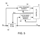
- Fig. 5 is a block diagram of the interference wave signal remover 50 according to the first embodiment.
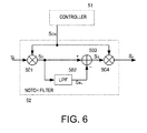
- Fig. 6 is a circuit block diagram of a notch filter 52 according to the first embodiment.
- Fig. 7 is a view illustrating scan frequency bands of an entire-range frequency scanner 53 and a local frequency scanner 54 and frequency bins (a plurality of frequency BIN).
- the interference wave signal remover 50 includes a controller 51, the notch filter 52, the entire-range frequency scanner 53 corresponding to the "first frequency scanner” of the present invention, and the local frequency scanner 54 corresponding to the "second frequency scanner” of the present invention.
- the controller 51 sets a scan frequency band BWf A and bandwidths BWf ABIN of scan frequencies BIN for the entire-range frequency scanner 53.
- the scan frequency band is set to be, for example, a reception band of the GNSS antenna 20 described above or the scan frequency band BWf A (see Fig. 7 ) having a carrier frequency of the GNSS signal as its central frequency and that has a possibility of influencing the acquisition and the tracking of the GNSS signal when an interference wave signal exists.
- the scan frequency band BWf A is set with a frequency band of 5 MHz.
- the width BWf ABIN of the scan frequency bin (scan frequency BIN) is set with a frequency band of 1 kHz.
- each frequency BIN (BIN A ) is set so that the scan frequency bands do not overlap with each other.
- the scan frequency band BWf A is divided into 5,000 frequency BIN (BIN A (1) to BIN A (5000)), a scanning period of time (integrating period of time) of the signals at each scan frequency BIN is 1 msec, and a total scanning period of time for the scan frequency band BWf A becomes 5 sec.
- the entire-range frequency scanner 53 is inputted with output signal So of the notch filter 52. Over the entire range of the scan frequency band BWf A , the entire-range frequency scanner 53 integrates signal intensities of the output signals So to calculate an integrated value (integrated signal) for each frequency BIN (each of BIN A (1) to BIN A (5000)). The entire-range frequency scanner 53 outputs the integrated signals of the respective frequency BIN (BIN A (1) to BIN A (5000)) to the controller 51.
- the entire-range frequency scanner 53 may compare the levels (signal intensities) of the integrated signals of the respective frequency BIN (BIN A (1) to BIN A (5000)) and outputs only a highest predetermined number (e.g., 8) of integrated signals in the descending order according to the level to the controller 51 instead of outputting all the integrated signals of the respective frequency BIN (BIN A (1) to BIN A (5000)).
- the controller 51 detects the frequency of the interference wave signal based on the intensities (signal levels) of the integrated signals of the respective frequency BIN (each of BIN A (1) to BIN A (5000)). Note that, when the limited number of integrated signals are inputted as described above, the controller 51 detects the frequency of the interference wave signal based on the intensities of these inputted integrated signals.
- the controller 51 sets an interference wave signal detection threshold and determines that the interference wave signal exists at the frequency BIN A where the integrated signal higher than the interference wave signal detection threshold is detected.
- this threshold may be set to a value obtained by integrating a predetermined value to an integrated value of the signal intensities of the GNSS signals in the output signals So in a predetermined period of time. Further, in a case where a reception status (e.g., C/No) of the GNSS signals can be determined, the threshold may be set according to the reception status.
- the controller 51 sets the interference wave signal frequency to the central frequency of the frequency BIN A where the existence of the interference wave signal is detected.
- the controller 51 detects a plurality of frequencies, it sets the interference wave signal frequency to the frequency with the highest signal intensity.
- the interference wave signal frequency may be set to the frequency with the longest detection period of time. Note that, the detection of such interference wave signal frequencies is not limited to be based on the integrated values of the signal intensities, and may use integrated values of signal powers, etc.
- the controller 51 sets an attenuation band setting signal S CN formed of the detected interference wave signal frequency.
- the controller 51 outputs the attenuation band setting signal S CN to the notch filter 52.
- the interference wave signal frequency detected by the controller 51 has a detection error only by the width BWf ABIN of the scan frequency BIN of the entire-range frequency scanner 53, and the attenuation frequency bandwidth is set to the width of this frequency error.
- the width BWf ABIN of the scan frequency BIN is 1 kHz
- the attenuation frequency bandwidth may be set to ⁇ 1 kHz.
- the notch filter 52 includes a down-converter 501, a low-pass filter 502 corresponding to the "baseband signal generator” of the present invention, an integrator 503 corresponding to the "subtracting element” of the present invention, and an up-converter 504.
- the down-converter 501 is inputted with an input signal S i that is the IF signal from the ADC 40 and the attenuation pole setting signal S CN from the controller 51.
- the down-converter 501 mixes the input signal S i with the attenuation pole setting signal S CN and outputs a down-converted signal S D .
- the down-converted signal S D is inputted to the low-pass filter 502 and the integrator 503.
- the low-pass filter 502 low-pass-filters the down-converted signal S D to output a baseband signal S BL .
- This baseband signal S BL corresponds to a baseband component of the signal obtained by mixing the input signal S i containing the interference wave signal with the attenuation pole setting signal S CN formed of the interference wave signal frequency. Therefore, the baseband signal S BL serves as a signal showing a state of the interference wave signal. That is, the signal intensity of the baseband signal S BL increases when the signal intensity of the interference wave signal is high, and the signal intensity of the baseband signal S BL becomes 0 (zero) when the interference wave signal is eliminated.
- This baseband signal S BL is inputted to the integrator 503.
- the integrator 503 subtracts the down-converted signal S D by the baseband signal S BL . By performing such processing, the component of the interference wave signal contained in the down-converted signal S D is removed. The integrator 503 outputs the subtracted signal S S to the up-converter 504.
- the up-converter 504 outputs the output signal So obtained by mixing the subtracted signal S S with the attenuation pole setting signal S CN to the acquirer/tracker 60.
- the output signals So inputted to the acquirer/tracker 60 are comprised of the signals which are the reception signals from which the interference wave signal is removed. That is, the output signals So formed only of the GNSS signals are outputted to the acquirer/tracker 60.
- the frequency scanning over the scan frequency band BWf A by the entire-range frequency scanner 53 as described above and the removal of the interference wave signal based on this scanning result are repeatedly performed. That is, as a certain one frequency scanning over the scan frequency band BWf A ends, the next frequency scanning over the scan frequency band BWf A simultaneously starts, and this is repeated. Then, the interference wave signal detection is performed for every one scanning and it is reflected onto the notch filter 52.
- the interference wave signal remover 50 of this embodiment performs processing of estimately calculating the frequency error corresponding to the detection error of the interference wave signal frequency detected based on the scanning result of the entire-range frequency scanner 53. Then, the interference wave signal remover 50 corrects the interference wave signal frequency by the estimately calculated frequency error and reflects it in the setting of the attenuation pole setting signal S CN to the notch filter 52.
- the controller 51 outputs the attenuation pole setting signal S CN described above to the notch filter 52 and sets a local scan frequency band BWf L and bandwidths BWf LBIN of local scan frequency BIN L (BIN L (M-2), BIN L (M-1), BIN L (M), BIN L (M+1), BIN L (M+2)) for the local frequency scanner 54.
- the local scan frequency band BWf L is set such that a frequency bandwidth of the entire scan band is narrower and the width of each frequency BIN is also narrower, with respect to the scan frequency band BWf A .
- the bandwidth of the local scan frequency band BWf L is 3/5 of the width BWf ABIN of the scan frequency BIN A of the entire-range frequency scanner 53
- the width of each local frequency BIN L is set to 1/5 of the width BWf ABIN of the scan frequency BIN A of the entire-range frequency scanner 53.
- the local scan frequency band BWf L is set to the frequency band of 0.6 kHz.
- the bandwidth BWf ABIN of the scan frequency BIN A is set to 1 kHz as described above
- the width BWf LBIN of the local scan frequency BIN L is set to the frequency of 0.2 kHz.
- the local scan frequency band BWf L is set such that the central frequency of the frequency BIN A detected to contain the interference wave signal by the entire-range frequency scanner 53 becomes the central frequency of a central local frequency BIN L among the group of the local frequency BIN L configuring the local scan frequency band BWf L .
- each local frequency BIN L is set such that the frequency bands partially overlap with each other between adjacent local frequency BIN L on the frequency axis. Specifically, as illustrated in Fig. 7 , the frequency bands overlap with each other between the local frequency BIN L by half thereof.
- 0.1 kHz of a higher side band of the local frequency BIN L (M-2) overlaps with 0.1 kHz of a lower side band of the local frequency BIN L (M-1).
- 0.1 kHz of a higher side band of the local frequency BIN L (M-1) overlaps with 0.1 kHz of a lower side band of the local frequency BIN L (M).
- 0.1 kHz of a higher side band of the local frequency BIN L (M) overlaps with 0.1 kHz of a lower side band of the local frequency BIN L (M+1).
- 0.1 kHz of a higher side band of the local frequency BIN L (M+1) overlaps with 0.1 kHz of a lower side band of the local frequency BIN L (M+2).
- the local frequency scanner 54 is inputted with the input signals S i of the notch filter 52. Over the entire range of the local scan frequency band BWf L , the local frequency scanner 54 integrates signal intensities of the input signals S i to calculate an integrated value (integrated signal) for each local scan frequency BIN L (each of BIN L (M-2), BIN L (M-1), BIN L (M), BIN L (M+1), BIN L (M+2)). In the setting example described above, the integrating time period of each local frequency BIN L by the local frequency scanner 54 is 5 msec.
- the frequency bands do not overlap among the three local scan frequency BIN L (M-2), BIN L (M) and BIN L (M+2), and thus, the total scanning time period for the entire local scan frequency band BWf L only requires 15 msec, resulting in a significantly short total scan time period compared to the total scanning time period (5 sec) with the entire-range frequency scanner 53. Moreover, in this case, the frequency resolution in the interference wave signal detection by the local frequency scanner 54 becomes 0.2 kHz ( ⁇ 0.1 kHz).
- the local frequency scanner 54 can continuously perform the scanning of the interference wave signal frequency in higher accuracy at a short cycle on the local frequency band which is a narrower frequency band than the scanning by the entire-range frequency scanner 53 but the interference wave signal exists therein.
- the local frequency scanner 54 outputs the integrated signals of the respective detected local scan frequency BIN L to the controller 51.
- the controller 51 estimately calculates a frequency error ⁇ f of the interference wave signal frequency by using the following principle, based on the integrated signals of the respective local scan frequency BIN L .
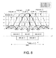
- Fig. 8 is a view for describing an estimate calculation concept of the frequency error ⁇ f of the interference wave signal frequency, which illustrates a relation among the frequency bands of the respective local scan frequency BIN L , respective sinc functions thereof, and a frequency f CW of a real interference wave signal CW.
- FS[f L (M)] indicates the sinc function of the local frequency BIN L (M) of which the central frequency is f(M)
- FS[f L (M+1)] indicates the sinc function of the local frequency BIN L (M+1) of which the central frequency is f(M+1) which is on the higher frequency side by one frequency BIN from the local frequency BIN L (M)
- FS[f L (M+2)] indicates the sinc function of the local frequency BIN L (M+2) of which the central frequency is f(M+2) which is on the higher frequency side by one frequency BIN from the local frequency BIN L (M+1).
- FS[f L (M-1)] indicates the sinc function of the local frequency BIN L (M-1) of which the central frequency is f(M-1) which is on the lower frequency side by one frequency BIN from the local frequency BIN L (M)
- FS[f L (M-2)] indicates the sinc function of the local frequency BIN L (M-2) of which the central frequency is f(M-2) which is on the lower frequency side by one frequency BIN from the local frequency BIN L (M-1).
- the central frequency f(M+1) f(M)+1/2T L
- the central frequency f(M+2) f(M)+1/T L
- the central frequency f(M-1) f(M)-1/2T L
- the central frequency f(M-2) f(M)-1/T L .
- Z CW (M) is the integrated signal level of the interference wave signal at the local frequency BIN L (M) where the interference wave signal is detected
- Z CW (M+1) is the integrated signal level of the interference wave signal at the local frequency BIN L (M+1)
- Z CW (M-1) is the integrated signal level of the interference wave signal at the local frequency BIN L (M-1).
- the controller 51 estimately calculates the frequency error ⁇ f by using that the frequency error ⁇ f at the local frequency BIN L (M) having the interference wave signal frequency detected by the entire-range frequency scanner 53 as its central frequency is dependent on the levels Z CW (M+1) and Z CW (M-1) of the integrated signal levels of the respective local frequency bands BIN L (M-1) and BIN L (M+1) adjacent to the local frequency BIN L (M), and the frequency error ⁇ f is in a relation based on the following Equation (3) with the levels Z CW (M+1) and Z CW (M-1) of the integrated signal levels of the respective local frequency bands BIN L (M-1) and BIN L (M+1).
- ⁇ f 1 2 ⁇ T ⁇ Z cw ⁇ M + 1 - Z cw ⁇ M - 1 Z cw ⁇ M + 1 + Z cw ⁇ M - 1
- the controller 51 corrects the estimately calculated frequency error ⁇ f by integrating it to the central frequency of the frequency BIN A detected to contain the interference wave signal by the entire-range frequency scanner 53, and sets the attenuation band setting signal S CN based on the corrected highly-accurate interference wave signal frequency f CW .
- the controller outputs the corrected attenuation band setting signal S CN to the notch filter 52.
- the interference wave signal frequency can be set highly accurately and the interference wave signal removal can be performed effectively.
- the frequency error ⁇ f can be detected promptly by partially overlapping the bands of the plurality of frequency BIN only in the local frequency band which is the narrow frequency band near the interference wave signal frequency roughly detected in the entire-range frequency scanning as described in this embodiment, and calculating the frequency error ⁇ f highly accurately. Therefore, highly-accurate update setting of the interference wave signal frequency can be performed promptly.
- the interference wave signal frequency can be detected highly accurately.
- the frequency scanning over such a local scan frequency band BWf L and the correction of the interference wave signal frequency based on this scanning result thereof are repeatedly performed similarly to the frequency scanning by the entire-range frequency scanner 53 described above and the interference wave signal removal based on this scanning result.
- the interference wave signal frequency is gradually tracked down and a more-accurate and effective attenuation frequency band can be set to the notch filter 52.
- the frequency error ⁇ f is used for the correction as it is; however, by using the following low-pass filtering, the interference wave signal frequency f CW may be calculated based on the frequency error ⁇ f.
- f CW t k f CW ⁇ t k - 1 + K ⁇ ⁇ f
- f CW (t k ) is an estimated interference wave signal frequency at a time point t k
- f CW (t k-1 ) is an estimated interference wave signal frequency at a time point t k-1 (sampling point immediately before the time point t k in an interference wave signal frequency estimation sampling cycle).
- K is a loop gain of a frequency estimation operation loop.
- the interference wave signal frequency can be estimately calculated more accurately.
- the local scan frequency band BWf L , the number of the local scan frequency BIN L , the width BWf LBIN of the local scan frequency BIN, and the overlapping frequency width of the adjacent local frequency BIN L may suitably be set according to the detection accuracy of the interference wave signal frequency and the attenuation frequency band and the like of the notch filter.
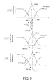
- Fig. 9 illustrates charts for describing a concept of tracking the frequency drift-type interference wave signal and removing it with the configuration and processing of this embodiment.
- CW(t 0 ) indicates the spectrum of the interference wave signal at a time point to and f CW (t 0 ) indicates the frequency thereof.
- ATT Notch (t 0 ) indicates the attenuation property of the notch filter 52 set at the time point to.
- BST(t 0 ) is an attenuation band of the notch filter 52 set at the time point t 0 .
- f DR (CW) indicates a frequency drift amount of the interference wave signal CW in the scanning time period of the entire local scan frequency band BWf L .
- ATT Notch (t 1L ) indicates the attenuation property of the notch filter 52 set at the time point t 1L .
- the interference wave signal CW(t 0 ) will be in the attenuation band BST(t 0 ) at this timing, and the interference wave signal CW(t 0 ) is removed by the notch filter 52.
- the frequency f CW (t 1L ) of the interference wave signal CW will be f CW (t 0 )+f DR (CW).
- the frequency drift amount f DR (CW) detected as above is detected by the controller 51 and processed similarly to the frequency error ⁇ f used for the correction of the interference wave signal frequency described above, and thus, it can be used for the update setting of the attenuation frequency band of the notch filter 52.
- the notch filter 52 is changed in its setting to a filter of which the central frequency is f CW (t 1L ) and the attenuation BST(t 1L ), and even the frequency drift-type interference wave signal can be removed continuously.
- the frequency scanning over such a local scan frequency band BWf L and the frequency detection (frequency tracking) of the interference wave signal based on the scanning result thereof are repeatedly performed similarly to the frequency scanning by the entire-range frequency scanner 53 described above and the interference wave signal removal based on the scanning result thereof.
- the local scan frequency band BWf L is more preferably suitably be set based on the drift speed of the interference wave signal and the attenuation frequency band of the notch filter.
- the notch filter 52 may output the baseband signal S BL to the controller 51.
- the controller 51 can perform the following processing.
- the controller 51 determines whether to continue or stop the output of the attenuation pole setting signal S CN based on the signal intensity of the baseband signal S BL which is outputted from the notch filter 52. Specifically, the controller 51 sets a determination threshold for the signal intensity of the baseband signal S BL , and if the signal intensity is higher than the determination threshold, the attenuation pole setting signal S CN is continuously outputted to the notch filter 52. Thus, the interference wave signal removal continues. If the signal intensity of the baseband signal S BL is lower than the determination threshold, the controller 51 stops the output of the attenuation pole setting signal S CN to the notch filter 52. Thus, the highly accurate detection of the interference wave signal frequency and the highly accurate tracking of the interference wave signal described above and, when the interference wave signal is eliminated, the interference wave signal attenuation function of the notch filter 52 can be stopped more rapidly.
- Fig. 10 is a block diagram of an interference wave signal remover 50A with multi-staged notch filters according to the second embodiment. Note that in Fig. 10 , a case where three notch filters are used is illustrated; however, it may be two, four or more.
- the configuration and processing for removing only one interference wave signal from the reception signals is described; however, a plurality of interference wave signals may actually be contained in the reception signals.
- the interference wave signal remover 50A having the following configuration may be used.
- the interference wave signal remover 50A includes a plurality of notch filters 521, 522 and 523. Moreover, the interference wave signal remover 50A includes a plurality of local frequency scanners 541, 542 and 543 corresponding to the number of notch filters.
- the notch filters 521, 522 and 523 have the same structure, which is the above- described structure illustrated in Fig. 6 .
- a down-converter side is connected with the ADC 40 (not illustrated) and an up-converter side is connected with a down-converter side of the notch filter 522.
- An up-converter side of the notch filter 522 is connected with a down-converter side of the notch filter 523, and an up-converter side of the notch filter 523 is connected with an acquirer/tracker 60 (not illustrated).
- the interference wave signal remover 50A having such a configuration operates as follows.
- the entire-range frequency scanner 53 calculates an integrated signal of the output signals So for every width BWf ABIN of the scan frequency BIN A over the entire range of the scan frequency band BWf A .
- the entire-range frequency scanner 53 outputs the integrated signals of the respective scan frequency BIN A to a controller 51A.
- the controller 51A detects the interference wave signal frequency based on the signal intensities of the integrated signals of the respective scan frequency BIN A from the entire-range frequency scanner 53 as described above.
- the controller 51A detects the interference wave signals for the number of notch filters provided to the interference wave signal remover 50A. If the number of detected interference wave signals is larger than the number of notch filters, the interference wave signals with a high signal intensity or having a long period of time of the signal intensities continuing to be higher than a threshold are preferentially detected.
- the controller 51A generates attenuation pole setting signals S CN1 , S CN2 and S CN3 for the respective detected interference wave signal frequencies, and outputs them to the respective notch filters 521, 522 and 523.
- the controller 51A outputs the attenuation pole setting signal S CN1 to the notch filter 521, the attenuation pole setting signal S CN2 to the notch filter 522, and the attenuation pole setting signal S CN3 to the notch filter 523, respectively.
- the attenuation pole setting signals may be generated by the number of interference wave signal frequencies.
- the notch filter 521 uses the attenuation pole setting signal S CN1 to remove a first interference wave signal from the input signal S i , and outputs the primary removal-processed signal S m1 to the notch filter 522.
- the notch filter 522 uses the attenuation pole setting signal S CN2 to remove a second interference wave signal from the primary removal-processed signal S m1 , and outputs the secondary removal-processed signal S m2 to the notch filter 523.
- the notch filter 523 uses the attenuation pole setting signal S CN3 to remove a third interference wave signal from the secondary removal-processed signal S m2 , and outputs the third removal-processed signal S m3 to the acquirer/tracker 60 as an output signal So.
- the controller 51A performs processing of outputting the attenuation range setting signal S CN1 to the notch filter 521 and sets a local scan frequency band BWf L1 and a bandwidth BWf LBIN1 of a local scan frequency BIN L1 to the local frequency scanner 541.
- the controller 51A performs processing of outputting the attenuation range setting signal S CN2 to the notch filter 522 and sets a local scan frequency band BWf L2 and a bandwidth BWf LBIN2 of a local scan frequency BIN L2 to the local frequency scanner 542.
- the controller 51A performs processing of outputting the attenuation range setting signal S CN3 to the notch filter 523 and sets a local scan frequency band BWf L3 and a bandwidth BWf LBIN3 of a local scan frequency BIN L3 to the local frequency scanner 543.
- the controller 51A sets the respective local frequency BIN L for the respective local scan frequency bands BWf L1 , BWf L2 and BWf L3 such that adjacent local frequency BIN L overlap with each other, similarly to the controller 51 described above.
- the local frequency scanner 541 is inputted with the input signals S i . Over the entire range of the local scan frequency band BWf L1 , the local frequency scanner 541 calculates an integrated signal of the input signals S i at each local scan frequency BIN L1 . The local frequency scanner 541 outputs the integrated signals of the respective local scan frequency BIN L1 to the controller 51A.
- the controller 51A detects a frequency error ⁇ f 1 based on signal intensities of the integrated signals of the respective local scan frequency BIN L1 from the local frequency scanner 541.
- the controller 51A performs a similar correction to the first embodiment on the interference wave signal frequency for the notch filter 521 detected based on the scanning result of the entire-range frequency scanner 53, by the frequency error ⁇ f 1 .
- the controller 51A updates the attenuation band setting signal S CN1 based on the corrected interference wave signal frequency, and outputs it to the notch filter 521.
- the local frequency scanner 542 is inputted with the primary removal-processed signals S m1 . Over the entire range of the local scan frequency band BWf L2 , the local frequency scanner 542 calculates an integrated signal of the primary removal-processed signals S m1 for each local scan frequency BIN L2 . The local frequency scanner 542 outputs the integrated signals of the respective local scan frequency BIN L2 to the controller 51A.
- the controller 51A detects a frequency error ⁇ f 2 based on signal intensities of the integrated signals of the respective local scan frequency BIN L2 from the local frequency scanner 542.
- the controller 51A performs a similar correction to the first embodiment on the interference wave signal frequency for the notch filter 522 detected based on the scanning result of the entire-range frequency scanner 53, by the frequency error ⁇ f 2 .
- the controller 51A updates the attenuation band setting signal S CN2 based on the corrected interference wave signal frequency, and outputs it to the notch filter 522.
- the local frequency scanner 543 is inputted with the secondary removal-processed signals S m2 . Over the entire range of the local scan frequency band BWf L3 , the local frequency scanner 543 calculates an integrated signal of the secondary removal-processed signals S m2 at each local scan frequency BIN L3 . The local frequency scanner 543 outputs the integrated signals of the respective local scan frequency BIN L3 to the controller 51A.
- the controller 51A detects a frequency error ⁇ f 3 based on signal intensities of the integrated signals of the respective local scan frequency BIN L3 from the local frequency scanner 543.
- the controller 51A performs a similar correction to the first embodiment on the interference wave signal frequency for the notch filter 523 detected based on the scanning result of the entire-range frequency scanner 53, by the frequency error ⁇ f 3 .
- the controller 51A updates the attenuation band setting signal S CN3 based on the corrected interference wave signal frequency, and outputs it to the notch filter 523.
- interference wave signal frequencies can be detected highly accurately from each of a plurality of interference wave signals.
- the effective interference wave signal removal by the notch filters becomes available, and an interference wave signal remover that is more practical can be realized.
- the tracking of the frequencies of the interference signals can be performed based on the frequency errors ⁇ f 1 , ⁇ f 2 and ⁇ f 3 outputted from the respective local frequency scanners 541, 542 and 543.
- Fig. 11 is a block diagram of an interference wave signal remover 50B with multi-staged notch filters according to the third embodiment. Note that, also in Fig. 11 , a case where three notch filters are used is illustrated; however, it may be two, four or more.
- the interference wave signal remover 50B of this embodiment is only different regarding the components for performing a local frequency scanning, and other configuration thereof is the same as that of the interference wave signal remover 50A described in the second embodiment.
- a multiplexer 551 is connected before a local frequency scanner 54 having a similar configuration to that of the above embodiments.
- a demultiplexer 552 is connected after the local frequency scanner 54.
- a selector 550 is inputted with scan target selected information, and information regarding a local scan frequency band BWf L and a bandwidth BWf LBIN of a local scan frequency BIN from a controller 51B.
- the scan target selected information is information for selecting which one of the plurality of notch filters 521, 522 and 523 of which the corresponding local frequency scanning is to be performed.
- the local scan frequency band BWf L and the bandwidth BWf LBIN of the local scan frequency BIN are set according to the selected notch filter.
- the selector 550 outputs the selected signal to the multiplexer 551 and the multiplexer 552 according to the scan target selected information. Moreover, the selector 550 sets the local scan frequency band BWf L and the bandwidth BWf LBIN of the local scan frequency BIN to the local frequency scanner 54. Specifically, the local frequency scanner 54 operates as follows by the processing of the selector 550.
- the multiplexer 551 When the notch filter 521 is selected, the multiplexer 551 performs a switch operation to input the input signals S i to the local frequency scanner 54.
- the local frequency scanner 54 scans frequencies in the local scan frequency band BWf L1 with a bandwidth BWF L1BIN of the local scan frequency BIN L1 .
- the demultiplexer 552 performs a switch operation to output the integrated signals of the respective local scan frequency BIN L1 to a setting module of the controller 51B for the notch filter 521.
- the multiplexer 551 When the notch filter 522 is selected, the multiplexer 551 performs a switch operation to input the primary removal-processed signals S m1 to the local frequency scanner 54.
- the local frequency scanner 54 scans frequencies in the local scan frequency band BWf L2 with a bandwidth BWf L2BIN of the local scan frequency BIN L2 .
- the demultiplexer 552 performs a switch operation to output the integrated signals of the respective local scan frequency BIN L2 to a setting module of the controller 51B for the notch filter 522.
- the multiplexer 551 When the notch filter 523 is selected, the multiplexer 551 performs a switch operation to input the secondary removal-processed signals S m2 to the local frequency scanner 54.
- the local frequency scanner 54 scans frequencies in the local scan frequency band BWf L3 with the bandwidth BWf L3BIN of the local scan frequency BIN L3 .
- the demultiplexer 552 performs a switch operation to output the integrated signals of the respective local scan frequency BIN L3 to a setting module of the controller 51B for the notch filter 523.
- the acquirer/tracker 60 is inputted with the signals only containing the GNSS signals, and thus, the acquisition and tracking ability can be improved. For example, the acquiring speed or the tracking speed improves, and the tracking accuracy can be improved. Moreover, due to the tracking accuracy improvement, the accuracy of the pseudorange and the like improves and the navigation message can surely be demodulated, and a highly accurate positioning result can be obtained.
- the mode of the processing of the controllers and the frequency scanners described in the respective embodiments above may be such that it is programmed to be saved in a hard disk, a ROM or the like, and executed by a computer.
- Fig. 12 is a flowchart illustrating an interference wave signal removing method according to the present invention. Note that, in Fig. 12 , the case where the number of notch filters is one is shown; however, when the number of notch filters is plural as described above, the method illustrated in Fig. 12 may be applied to each notch filter.
- an integrated signal intensity is detected for each scan frequency BIN having a bandwidth BWf ABIN (S101).
- the interference wave signal frequency f CW is detected based on the integrated signal intensities of the respective scan frequency BIN (S102).
- the local scan frequency band BWf L is set based on the interference wave signal frequency f CW , and the plurality of local frequency BIN each having a bandwidth BWf LBIN ( ⁇ BWf ABIN ) by which the local scan frequency band BWf L is divided are set.
- each local frequency BIN is set such that the frequency bands partially overlap with each other between adjacent local frequency BIN on the frequency axis (S103).
- the integrated signal intensity is detected for each local frequency BIN (S104).
- at least the integrated signal intensities of adjacent frequency BIN on the frequency axis among the local frequency BIN containing the interference wave signal frequency f CW are detected.
- the frequency error ⁇ f is calculated from the integrated signal intensities of adjacent frequency BIN on the frequency axis among the local frequency BIN containing the interference wave signal frequency f CW (S 105).
- the interference wave signal frequency f CW is corrected by integrating the frequency error ⁇ f to the interference wave signal frequency f CW (S106).
- the notch filtering is performed for removing components of the interference wave signal frequency f CW from the input signals S i (reception signals) by using the corrected interference wave signal frequency f CW (S107). Note that, this processing of calculating the detected frequency error ⁇ f of the interference wave signal frequency f CW , and correcting and update-setting the interference wave signal frequency f CW is performed continuously until the elimination of the relevant interference wave signal is detected.
- the frequency bands of the adjacent local scan frequency BIN L are set to overlap with each other in the setting of the local frequency BIN L of the local frequency scanner; however, also for the scan frequency BIN A of the entire-range frequency scanner 53, the frequency bands of the adjacent scan frequency BIN A are set to overlap with each other.
- GNSS reception apparatus 10 having the configuration as described above may be used in a movable terminal 1 as illustrated in Fig. 13.
- Fig. 13 is a block diagram of a main configuration of the mobile terminal 1 including the GNSS reception apparatus 10.
- the movable terminal 1 as illustrated in Fig. 13 is a mobile communicator such as a mobile phone, and it includes an GNSS antenna 20, the GNSS reception apparatus 10, an application processor 2, a mobile communication antenna 20M, and a mobile communication processor 3.
- the application processor 2 displays a self-device position and a self-device speed based on the obtained positioning result outputted from the GNSS reception apparatus 10, uses the same for navigation, and executes various applications using the self-device position.
- the mobile communication antenna 20M transceives a mobile communication signal (transmission signal and reception signal).
- the mobile communication processor 3 generates the transmission signal for mobile communication and demodulates the reception signal for mobile communication.
- the GNSS reception apparatus 10 including any one of the interference wave signal removers described above, even if the mobile communication signal is close to the frequency of the GNSS signal and has a high signal intensity, it is surely removed by the interference wave signal remover, and the reception sensitivity of the GNSS signal does not degrade. Thus, a highly accurate positioning result can be obtained and highly accurate position display and navigation and the like can be realized. Moreover, since it becomes possible to draw the frequency band of the mobile communication signal close to the frequency band of the GNSS signal, a useable frequency band of the mobile communication signal widens and the mobile terminal 1 can be configured to be more user-friendly.
- 100P Interference Wave Removing Device; 101P: Controller; 102P: Notch Filter; 103P: Frequency Analyzer; 104P: Frequency Scanner; 10: GNSS Receiving Apparatus; 20: GNSS Antenna; 30: RF Front End Circuit; 40: Analog-Digital Converter (ADC); 50, 50A, 50B: Interference Wave Signal Remover; 60: Acquirer/tracker; 70: Positioning Operator; 51, 51A, 51B: Controller; 52, 521, 522, 523: Notch Filter; 53: Entire-range Frequency Scanner; 54, 541, 542, 543: Local Frequency Scanner; 501: Down-Converter; 502: Low-Pass Filter; 503: Integrator; 504: Up-Converter; 550: Selector; 551: Multiplexer; 552: Demultiplexer; 1: Mobile Terminal; 2: Application Processor; 3: Mobile Communication Processor; and 20M: Mobile Communication Anten
Abstract
Description
- The present invention mainly relates to an interference wave signal removing device which removes an interference wave signals different from a signal and the like to be received, and a GNSS reception apparatus and a mobile terminal provided with the interference wave signal removing device.
- GNSS (Global Navigation Satellite Systems) such as a GPS (Global Positioning System) are used for, for example, positioning by receiving GNSS signals broadcasted from positioning satellites. Each GNSS signal is comprised of a spread spectrum signal which is code modulated by a pseudo noise.
- When receiving such a GNSS signal, if a signal other than the GNSS signal (hereinafter, referred to as the interference wave signal) is received, a disadvantage may be caused, for example, reception sensitivity to the GNSS signal degrades.
- Therefore,
Patent Document 1 andPatent Document 2 disclose interference wave signal removing devices for detecting and removing interference wave signals of which frequency bands are narrow (having narrow bands) different from GNSS signals.Fig. 1 is a block diagram of main circuits of the conventional interference wavesignal removing device 100P disclosed inPatent Document 1. - The conventional interference wave
signal removing device 100P disclosed inPatent Document 1 includes thecontroller 101P, thenotch filter 102P, thefrequency analyzer 103P, and thefrequency scanner 104P. Thecontroller 101P specifies a frequency of an interference wave signal based on a frequency spectrum of an input signal Si obtained from thefrequency analyzer 103P and a frequency spectrum of an output signal Sop obtained from thefrequency scanner 104P. Further specifically, the specification of the interference wave signal frequency is performed by the following processing. -
Fig. 2 is a view illustrating a concept of a plurality of frequency BIN set by theconventional frequency scanner 104P. As illustrated inFig. 2 , thefrequency scanner 104P divides an entire scan frequency BWfA into a plurality (5,000 inFig. 2 ) of frequency BIN each comprised of a frequency band BWfABIN, integrates signals per unit of the frequency BIN, and outputs the integrated signals of the respective frequency BIN to thecontroller 101P. Thecontroller 101P detects the frequency BIN of the integrated signals comprised of signal levels above a predetermined threshold and sets the central frequency of the frequency BIN to the interference wave signal frequency. - The
controller 101P adjusts the attenuation property of thenotch filter 102P to attenuate the interference wave signal frequency based on the information of the specified interference wave signal frequency. - Since the interference wave signal frequency is specified by such processing, in the method of
Patent Document 1, the frequency resolution for detecting the interference wave signal frequency is determined by the bandwidth of the frequency BIN. Therefore, if the bandwidth of the frequency BIN is wide, the interference wave signal frequency cannot be detected in high accuracy, and if the bandwidth of the frequency BIN is narrow, even though the interference wave signal frequency can be detected in high accuracy, the number of the frequency BIN increases and the detecting time length of the interference wave signal frequency increases. For example, when the bandwidth of the frequency BIN is set to 1/N, if the entire scan frequency band range is stable, the number of the frequency BIN to be scanned increases by N-times and the integrating time length for one frequency BIN increases by N-times. Therefore, the scanning period of time for the entire scan frequency band range increases by N2-times. - Therefore, in
Patent Document 2, the interference wave signal frequency is estimated by using a concept illustrated inFig. 3. Fig. 3 is a view for describing a frequency estimation concept inPatent Document 2. InFig. 3 , FS[f(n)] indicates a sinc function of the of the frequency BIN of which the central frequency is f(n). FS[f(n+1)] indicates a sinc function on the higher frequency side by one frequency BIN from the frequency BIN of FS[f(n)], where the central frequency is f(n+1). FS[f(n-1)] indicates a sinc function on the lower frequency side by one frequency BIN from the frequency BIN of FS[f(n)], where the central frequency is f(n-1). Here, when the integrating time period is T, the frequency bandwidth BW of each frequency BIN is 1/T, and the central frequency f(n+1)= f(n)+1/T and the central frequency f(n-1)= f(n)-1/T. - In
Patent Document 2, by using the setting of the frequency BIN illustrated inFig. 2 , the signal level ZCW(n) of the frequency BIN of FS[f(n)] where the interference wave signal is detected, and the signal level ZCW(n+1) of the frequency BIN of FS[f(n+1)] or the signal level ZCW(n-1) of the frequency BIN of FS[f(n-1)], an interference wave signal frequency fCW is estimately calculated based on Equation (1) if ZCW(n+ 1)>ZCW(n-1) or based on Equation (2) if ZCW(n+1)<ZCW(n-1).

-
- Patent Document 1:
US 2008/0240315 - Patent Document 2:
US 6219376 - However, in the method of using Equations (1) and (2) described above, non-linear comparison processing is required to be performed, when a signal power-to-noise power ratio SNR, more accurately, a jammer power-to-noise power ratio JNR is reduced, a squaring loss caused by the non-linear processing increases. Therefore, in the method of using Equations (1) and (2) described above by comparison therebetween, an estimation error of the interference wave frequency becomes large.
- Therefore, the present invention aims to provide an interference wave signal removing device for estimating an interference wave signal frequency promptly and highly accurately and performing an interference wave signal removal without being influenced by a reception environment.
- This invention relates to an interference wave signal removing device for removing an interference wave signal different from a desired signal that is contained in reception signals. This interference wave signal removing device includes a notch filter adjustable of an attenuation frequency band, a frequency scanner, and a controller. The frequency scanner outputs integrated signals of the reception signals at respective frequency bins which having a predetermined frequency width and partially overlapping with each other in a scan frequency band. The controller estimately calculates an error of the interference wave signal frequency based on the intensities of the integrated signals of the respective frequency bins, corrects the detected interference wave signal frequency by the error, and sets the attenuation frequency band of the notch filter.
- Moreover, the controller of the interference wave signal removing device of this invention may set the interference wave signal frequency to be a central frequency of the frequency bin where the intensity of the integrated signal of each frequency bin is higher than a predetermined threshold, and the controller may calculate the error of the interference wave signal frequency based on the intensities of the integrated signals of frequency bins adjacent to the frequency bin of the interference wave signal frequency on a frequency axis.
- Moreover, the controller of the interference wave signal removing device of this invention may correct the interference wave signal frequency by integrating the error to the interference wave signal frequency.
- With this configuration, the error of the interference wave signal frequency is directly calculated based on the intensities of the integrated signals of the plurality of frequency bins adjacent to the frequency bin where the interference wave signal is detected. Therefore, the interference wave frequency can be corrected without performing the non-linear comparison as the conventional art, and the interference wave frequency can be detected highly accurately. Thus, the attenuation frequency band of the notch filter can be set highly accurately.
- Further, with the interference wave signal removing device of this invention, the frequency scanner may include a first frequency scanner and a second frequency scanner. The first frequency scanner may frequency-scan the output signals that are the reception signals outputted through the notch filter in a first frequency band, and output first integrated signals of respective frequency bins that have frequency bands non-overlapped with each other and are each formed of a first frequency bandwidth. The second frequency scanner may frequency-scan the reception signals in a second frequency band comprised of a frequency band narrower than the first frequency band and based on the attenuation frequency band, and output second integrated signals at respective frequency bins having frequency bands that partially overlap with each other and are each formed of a second frequency bandwidth. The controller may detect the interference wave signal frequency based on the first integrated signals and estimately calculate the error of the interference wave signal based on the second integrated signals.
- With this configuration, the detection of the interference wave frequency over the entire range of the frequency band to be scanned is performed by the first frequency scanner. Then, the local frequency band is set for the detected interference wave frequency, and it is scanned by the second frequency scanner and utilized for the error detection. Thus, since a frequency BIN with a narrow frequency bandwidth is used only for the error detection, a rapid detection of the interference wave signal frequency and a highly accurate detection (correction) can be realized.
- Moreover, with the interference wave signal removing device of this invention, the frequency width of the second frequency band may be set narrower than the frequency width of the first frequency band. With this configuration, the width of the frequency BIN used for calculating the error frequency becomes narrow, and the error frequency can be detected in higher accuracy.
- Moreover, with the interference wave signal removing device of this invention, the notch filter may include a plurality of notch filters and are connected in series. The second frequency scanner may be provided for each of the plurality of notch filters. Each of the second frequency scanners set for each notch filter may scan the input signals of the notch filter as a setting target in the second frequency band set to each second frequency scanner, and each second frequency scanner may output the respective second integrated signals of the respective frequency bins that are each formed of the second frequency bandwidth. Based on the second integrated signals outputted from each second frequency scanner, the controller may estimately calculate the error of the interference wave signal frequency individually and sets the attenuation frequency band to each notch filter.
- With this configuration, even when a plurality of interference wave signals exist, the detection and the correction of the frequency are performed on each of the interference wave signals. Therefore, even if a plurality of interference wave signals exist, the attenuation frequency band can be set highly accurately to each of the plurality of notch filters.
- Moreover, with the interference wave signal removing device of this invention, the controller may perform low-pass filtering on the error. With this configuration, the measurement noise of the estimately-calculated frequency error can be suppressed, and the interference wave frequency can be corrected highly accurately.
- Moreover, with the interference wave signal removing device of this invention, the notch filter may include a down-converter for multiplying the input signal by an attenuation pole setting signal for setting the attenuation frequency band outputted from the controller, a baseband signal generator for generating a baseband signal by extracting a baseband component of the down-converted signal, a subtracting element for subtracting the baseband signal from the down-converted signal, and an up-converter for multiplying the subtracted signal by the attenuation pole setting signal. The notch filter may output the baseband signal to the controller. The controller may detect removal of the interference wave signal based on the baseband signal and, when the successful removal of the interference wave signal is detected, release the setting of the attenuation frequency band to the notch filter.
- With this configuration, a specific configuration of the notch filter is shown. Moreover, with this configuration, the baseband component of the down-converted signal obtained by multiplying the input signal by the attenuation pole setting signal corresponds to the frequency component of the interference wave. Therefore, by outputting the baseband signal to the controller, the controller can accurately detect the continuation and the removal of the interference wave signal. That is, highly accurate setting of the interference wave signal frequency described above becomes available, and the removal of the interference wave signal can be detected promptly.
- Further, with this configuration, a circuit configuration only for extracting the frequency component of the interference wave signal from the input signals is not required. Therefore, an interference wave signal removing device can be realized with a simpler configuration. Moreover, this configuration is further effective also in a case where a plurality of stages of notch filters exist and the continuation and the removal of a plurality of interference wave signals are checked individually.
- Furthermore, this invention relates to a GNSS reception apparatus for receiving and demodulating GNSS signals. The GNSS reception apparatus includes the interference wave signal removing device described above, a receiver, an acquirer/tracker, and a positioning operator. The receiver is connected before the interference wave signal removing device. The receiver receives GNSS signals as desired signals, generates GNSS reception signals, and outputs them to the interference wave signal removing device. The acquirer/tracker acquires and tracks the GNSS reception signals after the interference wave signal removal.
- With this configuration, the attenuation frequency band of the notch filter is set highly accurately and the interference wave signal is surely removed as described above. Therefore, the speed and the accuracy of acquiring and tracking thereof improve. The positioning operator may perform positioning by using the tracked GNSS signals. Moreover, due to the improvement of the speed and the accuracy of the acquiring and the tracking, the converging speed of the positioning operation and the accuracy of the positioning result improve.
- Furthermore, this invention relates to a mobile terminal. The mobile terminal includes the GNSS reception apparatus described above and an application processor for performing a predetermined application by using the positioning operation result of the positioning operator. With this configuration, the GNSS reception apparatus described above is provided, and the highly accurate positioning result can be utilized. Therefore, the performance of the application using the positioning result improves.
- According to this invention, an interference wave frequency can be detected highly accurately and the interference wave can surely be removed.
-
-
Fig. 1 is a block diagram of main circuits of the conventional interference wavesignal removing device 100P disclosed inPatent Document 1. -
Fig. 2 is a view illustrating a concept of a plurality of frequency BIN set by theconventional frequency scanner 104P. -
Fig. 3 is a view for describing a frequency estimation concept inPatent Document 2. -
Fig. 4 is a block diagram of aGNSS reception apparatus 10 according to a first embodiment. -
Fig. 5 is a block diagram of an interferencewave signal remover 50 according to the first embodiment. -
Fig. 6 is a circuit block diagram of anotch filter 52 according to the first embodiment. -
Fig. 7 is a view illustrating scan frequency bands of an entire-range frequency scanner 53 and alocal frequency scanner 54 and a plurality of frequency BIN (frequency bins). -
Fig. 8 is a view for describing an estimate calculation concept of a frequency error δf of an interference wave signal frequency. -
Fig. 9 illustrates charts for describing a concept of tracking a frequency drift-type interference wave signal and removing it with a configuration and processing of the first embodiment. -
Fig. 10 is a block diagram of an interference wave signal remover 50A with multi-staged notch filters according to a second embodiment. -
Fig. 11 is a block diagram of an interference wave signal remover 50B with multi-staged notch filters according to a third embodiment. -
Fig. 12 is a flowchart illustrating an interference wave signal removing method according to the present invention. -
Fig. 13 is a block diagram of a main configuration of amobile terminal 1 including theGNSS reception apparatus 10. - An interference wave signal removing device according to a first embodiment of the present invention is described with reference to the drawings. The interference wave signal removing device of this embodiment functions as an interference wave signal remover 50 of a
GNSS reception apparatus 10. -
Fig. 4 is a block diagram of aGNSS reception apparatus 10 according to the first embodiment. TheGNSS reception apparatus 10 includes aGNSS antenna 20, an RFfront end circuit 30, an analog-to-digital converter (ADC) 40, the interferencewave signal remover 50, an acquirer/tracker 60, and apositioning operator 70. TheGNSS antenna 20 receives wireless signals including GNSS signals and outputs them to the RFfront end circuit 30. - Each GNSS signal is a signal obtained by code-modulating a carrier wave signal with a pseudo noise, and is a spread spectrum signal in which frequency components spread in a wide band and each frequency component has a low spectral intensity. Moreover, for example, when it is an L1 wave signal of GPS signals, a navigation message is superimposed thereon.
- Here, when an interference wave signal exists and a frequency of the interference wave signal is within a reception frequency band of the antenna, the reception signals contain the interference wave signal on top of the GNSS signal.
- The RF
front end circuit 30 converts the reception signal into an intermediate frequency signal (IF signal) and outputs it to theADC 40. TheADC 40 samples the analog IF signal at a predetermined sampling interval to generate a digital IF signal and outputs it to the interferencewave signal remover 50. - The interference
wave signal remover 50 detects the frequency of the interference wave signal based on a scanning result for the entire-range of a scan frequency band. The interferencewave signal remover 50 calculates a frequency error of the detected interference wave signal frequency within a local frequency range based on the detected interference wave signal frequency. The interferencewave signal remover 50 corrects the detected interference wave frequency by the frequency error and sets an attenuation frequency band of the notch filter used for an interference wave removal based on the corrected interference wave signal frequency. The notch filter removes the interference wave signal from the IF signals and outputs the signals only containing the GNSS signals to the acquirer/tracker 60. - The acquirer/
tracker 60 performs a correlation between each output signal from the interferencewave signal remover 50, which is the GNSS signal, and a reference signal to acquire and track a carrier phase and a code phase, and outputs the tracking result (correlation result) to thepositioning operator 70. Thepositioning operator 70 performs a positioning operation by calculating a peudorange or the like based on the correlation result. Here, if the navigation message is superimposed on the GNSS signals, the navigation message is demodulated and used for the positioning operation. - By using the
GNSS reception apparatus 10 with such a configuration, since the GNSS signals are inputted into the acquirer/tracker 60 in a state where the interference wave signal is removed therefrom, the acquisition and the tracking are facilitated and a highly accurate positioning operation result can be obtained. - Next, the configuration and the processing of the interference
wave signal remover 50 are described further in detail. In this embodiment, a case where a single-stage notch filter is provided to the interferencewave signal remover 50 is described.Fig. 5 is a block diagram of the interferencewave signal remover 50 according to the first embodiment.Fig. 6 is a circuit block diagram of anotch filter 52 according to the first embodiment.Fig. 7 is a view illustrating scan frequency bands of an entire-range frequency scanner 53 and alocal frequency scanner 54 and frequency bins (a plurality of frequency BIN). - The interference
wave signal remover 50 includes acontroller 51, thenotch filter 52, the entire-range frequency scanner 53 corresponding to the "first frequency scanner" of the present invention, and thelocal frequency scanner 54 corresponding to the "second frequency scanner" of the present invention. - The
controller 51 sets a scan frequency band BWfA and bandwidths BWfABIN of scan frequencies BIN for the entire-range frequency scanner 53. The scan frequency band is set to be, for example, a reception band of theGNSS antenna 20 described above or the scan frequency band BWfA (seeFig. 7 ) having a carrier frequency of the GNSS signal as its central frequency and that has a possibility of influencing the acquisition and the tracking of the GNSS signal when an interference wave signal exists. - For example, the scan frequency band BWfA is set with a frequency band of 5 MHz. Moreover, the width BWfABIN of the scan frequency bin (scan frequency BIN) is set with a frequency band of 1 kHz. Further, each frequency BIN (BINA) is set so that the scan frequency bands do not overlap with each other. Thus, the scan frequency band BWfA is divided into 5,000 frequency BIN (BINA(1) to BINA(5000)), a scanning period of time (integrating period of time) of the signals at each scan frequency BIN is 1 msec, and a total scanning period of time for the scan frequency band BWfA becomes 5 sec.
- The entire-
range frequency scanner 53 is inputted with output signal So of thenotch filter 52. Over the entire range of the scan frequency band BWfA, the entire-range frequency scanner 53 integrates signal intensities of the output signals So to calculate an integrated value (integrated signal) for each frequency BIN (each of BINA(1) to BINA(5000)). The entire-range frequency scanner 53 outputs the integrated signals of the respective frequency BIN (BINA(1) to BINA(5000)) to thecontroller 51. Here, the entire-range frequency scanner 53 may compare the levels (signal intensities) of the integrated signals of the respective frequency BIN (BINA(1) to BINA(5000)) and outputs only a highest predetermined number (e.g., 8) of integrated signals in the descending order according to the level to thecontroller 51 instead of outputting all the integrated signals of the respective frequency BIN (BINA(1) to BINA(5000)). - The
controller 51 detects the frequency of the interference wave signal based on the intensities (signal levels) of the integrated signals of the respective frequency BIN (each of BINA(1) to BINA(5000)). Note that, when the limited number of integrated signals are inputted as described above, thecontroller 51 detects the frequency of the interference wave signal based on the intensities of these inputted integrated signals. - Specifically, for example, the
controller 51 sets an interference wave signal detection threshold and determines that the interference wave signal exists at the frequency BINA where the integrated signal higher than the interference wave signal detection threshold is detected. Note that, for example, this threshold may be set to a value obtained by integrating a predetermined value to an integrated value of the signal intensities of the GNSS signals in the output signals So in a predetermined period of time. Further, in a case where a reception status (e.g., C/No) of the GNSS signals can be determined, the threshold may be set according to the reception status. - The
controller 51 sets the interference wave signal frequency to the central frequency of the frequency BINA where the existence of the interference wave signal is detected. Here, in a case where thecontroller 51 detects a plurality of frequencies, it sets the interference wave signal frequency to the frequency with the highest signal intensity. Alternatively, if the detection results are sequentially obtained, the interference wave signal frequency may be set to the frequency with the longest detection period of time. Note that, the detection of such interference wave signal frequencies is not limited to be based on the integrated values of the signal intensities, and may use integrated values of signal powers, etc. - The
controller 51 sets an attenuation band setting signal SCN formed of the detected interference wave signal frequency. Thecontroller 51 outputs the attenuation band setting signal SCN to thenotch filter 52. - Here, the interference wave signal frequency detected by the
controller 51 has a detection error only by the width BWfABIN of the scan frequency BIN of the entire-range frequency scanner 53, and the attenuation frequency bandwidth is set to the width of this frequency error. For example, if the width BWfABIN of the scan frequency BIN is 1 kHz, the attenuation frequency bandwidth may be set to ±1 kHz. Thus, even in the state of including the detection error, the degradation of the interference wave signal removing effect produced by thenotch filter 52 can be suppressed. - The
notch filter 52 includes a down-converter 501, a low-pass filter 502 corresponding to the "baseband signal generator" of the present invention, anintegrator 503 corresponding to the "subtracting element" of the present invention, and an up-converter 504. - The down-
converter 501 is inputted with an input signal Si that is the IF signal from theADC 40 and the attenuation pole setting signal SCN from thecontroller 51. The down-converter 501 mixes the input signal Si with the attenuation pole setting signal SCN and outputs a down-converted signal SD. The down-converted signal SD is inputted to the low-pass filter 502 and theintegrator 503. - The low-
pass filter 502 low-pass-filters the down-converted signal SD to output a baseband signal SBL. This baseband signal SBL corresponds to a baseband component of the signal obtained by mixing the input signal Si containing the interference wave signal with the attenuation pole setting signal SCN formed of the interference wave signal frequency. Therefore, the baseband signal SBL serves as a signal showing a state of the interference wave signal. That is, the signal intensity of the baseband signal SBL increases when the signal intensity of the interference wave signal is high, and the signal intensity of the baseband signal SBL becomes 0 (zero) when the interference wave signal is eliminated. This baseband signal SBL is inputted to theintegrator 503. - The
integrator 503 subtracts the down-converted signal SD by the baseband signal SBL. By performing such processing, the component of the interference wave signal contained in the down-converted signal SD is removed. Theintegrator 503 outputs the subtracted signal SS to the up-converter 504. - The up-
converter 504 outputs the output signal So obtained by mixing the subtracted signal SS with the attenuation pole setting signal SCN to the acquirer/tracker 60. - Thus, when the interference wave signal is contained in the reception signals of the
GNSS antenna 20, the output signals So inputted to the acquirer/tracker 60 are comprised of the signals which are the reception signals from which the interference wave signal is removed. That is, the output signals So formed only of the GNSS signals are outputted to the acquirer/tracker 60. - The frequency scanning over the scan frequency band BWfA by the entire-
range frequency scanner 53 as described above and the removal of the interference wave signal based on this scanning result are repeatedly performed. That is, as a certain one frequency scanning over the scan frequency band BWfA ends, the next frequency scanning over the scan frequency band BWfA simultaneously starts, and this is repeated. Then, the interference wave signal detection is performed for every one scanning and it is reflected onto thenotch filter 52. - On top of such an entire-range frequency scanning, the interference wave signal remover 50 of this embodiment performs processing of estimately calculating the frequency error corresponding to the detection error of the interference wave signal frequency detected based on the scanning result of the entire-
range frequency scanner 53. Then, the interferencewave signal remover 50 corrects the interference wave signal frequency by the estimately calculated frequency error and reflects it in the setting of the attenuation pole setting signal SCN to thenotch filter 52. - The
controller 51 outputs the attenuation pole setting signal SCN described above to thenotch filter 52 and sets a local scan frequency band BWfL and bandwidths BWfLBIN of local scan frequency BINL (BINL(M-2), BINL(M-1), BINL(M), BINL(M+1), BINL(M+2)) for thelocal frequency scanner 54. - As illustrated in
Fig. 7 , the local scan frequency band BWfL is set such that a frequency bandwidth of the entire scan band is narrower and the width of each frequency BIN is also narrower, with respect to the scan frequency band BWfA. For example, in the example ofFig. 7 , the bandwidth of the local scan frequency band BWfL is 3/5 of the width BWfABIN of the scan frequency BINA of the entire-range frequency scanner 53, and the width of each local frequency BINL is set to 1/5 of the width BWfABIN of the scan frequency BINA of the entire-range frequency scanner 53. - More specifically, for example, when the scan frequency band BWfA is set to 5 MHz as described above, the local scan frequency band BWfL is set to the frequency band of 0.6 kHz. The bandwidth BWfABIN of the scan frequency BINA is set to 1 kHz as described above, the width BWfLBIN of the local scan frequency BINL is set to the frequency of 0.2 kHz.
- Further, the local scan frequency band BWfL is set such that the central frequency of the frequency BINA detected to contain the interference wave signal by the entire-
range frequency scanner 53 becomes the central frequency of a central local frequency BINL among the group of the local frequency BINL configuring the local scan frequency band BWfL. - Moreover, each local frequency BINL is set such that the frequency bands partially overlap with each other between adjacent local frequency BINL on the frequency axis. Specifically, as illustrated in
Fig. 7 , the frequency bands overlap with each other between the local frequency BINL by half thereof. Under the above-described setting condition, 0.1 kHz of a higher side band of the local frequency BINL(M-2) overlaps with 0.1 kHz of a lower side band of the local frequency BINL(M-1). 0.1 kHz of a higher side band of the local frequency BINL(M-1) overlaps with 0.1 kHz of a lower side band of the local frequency BINL(M). 0.1 kHz of a higher side band of the local frequency BINL(M) overlaps with 0.1 kHz of a lower side band of the local frequency BINL(M+1). 0.1 kHz of a higher side band of the local frequency BINL(M+1) overlaps with 0.1 kHz of a lower side band of the local frequency BINL(M+2). - The
local frequency scanner 54 is inputted with the input signals Si of thenotch filter 52. Over the entire range of the local scan frequency band BWfL, thelocal frequency scanner 54 integrates signal intensities of the input signals Si to calculate an integrated value (integrated signal) for each local scan frequency BINL (each of BINL(M-2), BINL(M-1), BINL(M), BINL(M+1), BINL(M+2)). In the setting example described above, the integrating time period of each local frequency BINL by thelocal frequency scanner 54 is 5 msec. Here, the frequency bands do not overlap among the three local scan frequency BINL(M-2), BINL(M) and BINL(M+2), and thus, the total scanning time period for the entire local scan frequency band BWfL only requires 15 msec, resulting in a significantly short total scan time period compared to the total scanning time period (5 sec) with the entire-range frequency scanner 53. Moreover, in this case, the frequency resolution in the interference wave signal detection by thelocal frequency scanner 54 becomes 0.2 kHz (±0.1 kHz). - Thus, the
local frequency scanner 54 can continuously perform the scanning of the interference wave signal frequency in higher accuracy at a short cycle on the local frequency band which is a narrower frequency band than the scanning by the entire-range frequency scanner 53 but the interference wave signal exists therein. - The
local frequency scanner 54 outputs the integrated signals of the respective detected local scan frequency BINL to thecontroller 51. - The
controller 51 estimately calculates a frequency error δf of the interference wave signal frequency by using the following principle, based on the integrated signals of the respective local scan frequency BINL.Fig. 8 is a view for describing an estimate calculation concept of the frequency error δf of the interference wave signal frequency, which illustrates a relation among the frequency bands of the respective local scan frequency BINL, respective sinc functions thereof, and a frequency fCW of a real interference wave signal CW. - In
Fig. 8 , FS[fL(M)] indicates the sinc function of the local frequency BINL(M) of which the central frequency is f(M), and FS[fL(M+1)] indicates the sinc function of the local frequency BINL(M+1) of which the central frequency is f(M+1) which is on the higher frequency side by one frequency BIN from the local frequency BINL(M), and FS[fL(M+2)] indicates the sinc function of the local frequency BINL(M+2) of which the central frequency is f(M+2) which is on the higher frequency side by one frequency BIN from the local frequency BINL(M+1). FS[fL(M-1)] indicates the sinc function of the local frequency BINL(M-1) of which the central frequency is f(M-1) which is on the lower frequency side by one frequency BIN from the local frequency BINL(M), and FS[fL(M-2)] indicates the sinc function of the local frequency BINL(M-2) of which the central frequency is f(M-2) which is on the lower frequency side by one frequency BIN from the local frequency BINL(M-1). Here, when the integrating time period is T, the frequency bandwidth BW of each frequency BIN is 1/TL(=1/T), the central frequency f(M+1)= f(M)+1/2TL, the central frequency f(M+2)= f(M)+1/TL, the central frequency f(M-1)= f(M)-1/2TL, and the central frequency f(M-2)= f(M)-1/TL. Moreover, ZCW(M) is the integrated signal level of the interference wave signal at the local frequency BINL(M) where the interference wave signal is detected, ZCW(M+1) is the integrated signal level of the interference wave signal at the local frequency BINL(M+1), and ZCW(M-1) is the integrated signal level of the interference wave signal at the local frequency BINL(M-1). - The
controller 51 estimately calculates the frequency error δf by using that the frequency error δf at the local frequency BINL(M) having the interference wave signal frequency detected by the entire-range frequency scanner 53 as its central frequency is dependent on the levels ZCW(M+1) and ZCW(M-1) of the integrated signal levels of the respective local frequency bands BINL(M-1) and BINL(M+1) adjacent to the local frequency BINL(M), and the frequency error δf is in a relation based on the following Equation (3) with the levels ZCW(M+1) and ZCW(M-1) of the integrated signal levels of the respective local frequency bands BINL(M-1) and BINL(M+1).
- The
controller 51 corrects the estimately calculated frequency error δf by integrating it to the central frequency of the frequency BINA detected to contain the interference wave signal by the entire-range frequency scanner 53, and sets the attenuation band setting signal SCN based on the corrected highly-accurate interference wave signal frequency fCW. The controller outputs the corrected attenuation band setting signal SCN to thenotch filter 52. Thus, the attenuation frequency band based on the interference wave signal frequency detected highly accurately is set to thenotch filter 52, and therefore, the interference wave signal can more surely and effectively be removed. - As described above, by using the configuration of this embodiment, the interference wave signal frequency can be set highly accurately and the interference wave signal removal can be performed effectively. Particularly, the frequency error δf can be detected promptly by partially overlapping the bands of the plurality of frequency BIN only in the local frequency band which is the narrow frequency band near the interference wave signal frequency roughly detected in the entire-range frequency scanning as described in this embodiment, and calculating the frequency error δf highly accurately. Therefore, highly-accurate update setting of the interference wave signal frequency can be performed promptly.
- Moreover, since non-linear selecting operation is not used, even if the JNR degrades, the interference wave signal frequency can be detected highly accurately.
- Note that, the frequency scanning over such a local scan frequency band BWfL and the correction of the interference wave signal frequency based on this scanning result thereof are repeatedly performed similarly to the frequency scanning by the entire-
range frequency scanner 53 described above and the interference wave signal removal based on this scanning result. Thus, the interference wave signal frequency is gradually tracked down and a more-accurate and effective attenuation frequency band can be set to thenotch filter 52. - Moreover, in the description above, the frequency error δf is used for the correction as it is; however, by using the following low-pass filtering, the interference wave signal frequency fCW may be calculated based on the frequency error δf.

- By performing such low-pass filtering, the effect of the measurement noise can be suppressed. Thus, the interference wave signal frequency can be estimately calculated more accurately.
- Further, the local scan frequency band BWfL, the number of the local scan frequency BINL, the width BWfLBIN of the local scan frequency BIN, and the overlapping frequency width of the adjacent local frequency BINL may suitably be set according to the detection accuracy of the interference wave signal frequency and the attenuation frequency band and the like of the notch filter.
- Moreover, the calculation of such a frequency error δf can also be used in a case of tracking a frequency drift-type interference wave signal of which the frequency drifts with time, while detecting a frequency thereof highly accurately.
Fig. 9 illustrates charts for describing a concept of tracking the frequency drift-type interference wave signal and removing it with the configuration and processing of this embodiment. - In
Fig. 9 , CW(t0) indicates the spectrum of the interference wave signal at a time point to and fCW(t0) indicates the frequency thereof. ATTNotch(t0) indicates the attenuation property of thenotch filter 52 set at the time point to. BST(t0) is an attenuation band of thenotch filter 52 set at the time point t0. fDR(CW) indicates a frequency drift amount of the interference wave signal CW in the scanning time period of the entire local scan frequency band BWfL. - CW(t1L) indicates the spectrum of the interference wave signal at the time point t1L (=to+(total scanning time period of the entire local scan frequency band BWfL)), and fCW(t1L) indicates the frequency thereof. ATTNotch(t1L) indicates the attenuation property of the
notch filter 52 set at the time point t1L. - Firstly, as the frequency fCW(t0) of the interference wave signal is detected at a time point T=t0 and the attenuation band BST(t0) of the
notch filter 52 is set by having the frequency fCW(t0) as the central frequency, the interference wave signal CW(t0) will be in the attenuation band BST(t0) at this timing, and the interference wave signal CW(t0) is removed by thenotch filter 52. - When the detected interference wave signal is the frequency drift-type, at the timing when the time point T=t1L which is after the total scanning time period of the entire local scan frequency band BWfL, the frequency fCW(t1L) of the interference wave signal CW will be fCW(t0)+fDR(CW).
- Here, if the frequency bandwidth of the attenuation band BST of the
notch filter 52 is suitably set, as illustrated in the middle row ofFig. 9 , even after the frequency drift at the timing when the time point T=t1L, the interference wave signal CW(t1L) is substantially entirely in the attenuation band BST(t0) and removed by thenotch filter 52. - Moreover, the frequency drift amount fDR(CW) at the frequency drift speed of the interference wave signal can be considered as the frequency error δf at the timing when the time point T=t1L with respect to the interference wave signal frequency at the timing when the time point T=t0.
- Therefore, the frequency drift amount fDR(CW) detected as above is detected by the
controller 51 and processed similarly to the frequency error δf used for the correction of the interference wave signal frequency described above, and thus, it can be used for the update setting of the attenuation frequency band of thenotch filter 52. - Thus, as illustrated in the lowest row of
Fig. 9 , thenotch filter 52 is changed in its setting to a filter of which the central frequency is fCW(t1L) and the attenuation BST(t1L), and even the frequency drift-type interference wave signal can be removed continuously. - The frequency scanning over such a local scan frequency band BWfL and the frequency detection (frequency tracking) of the interference wave signal based on the scanning result thereof are repeatedly performed similarly to the frequency scanning by the entire-
range frequency scanner 53 described above and the interference wave signal removal based on the scanning result thereof. Thus, even if the interference wave signal is the frequency drift-type, the frequency thereof can be surely tracked and be removed continuously. Note that, when tracking the interference wave signal, the local scan frequency band BWfL is more preferably suitably be set based on the drift speed of the interference wave signal and the attenuation frequency band of the notch filter. - Moreover, by using the configuration and the processing described above, since a time difference is not used for the detection of the frequency error, there is no limitation that a time interval needs to be within one cycle of the signal as the normal FLL (Frequency Locked Loop). Therefore, a frequency drawing range will not be lost even if the time interval of the frequency error detection is long, and thus, the operation rate of tracking the frequency can be reduced. Thus, an increase of a signal processing load can be prevented.
- Moreover, in the above configuration, the
notch filter 52 may output the baseband signal SBL to thecontroller 51. In this case, thecontroller 51 can perform the following processing. - The
controller 51 determines whether to continue or stop the output of the attenuation pole setting signal SCN based on the signal intensity of the baseband signal SBL which is outputted from thenotch filter 52. Specifically, thecontroller 51 sets a determination threshold for the signal intensity of the baseband signal SBL, and if the signal intensity is higher than the determination threshold, the attenuation pole setting signal SCN is continuously outputted to thenotch filter 52. Thus, the interference wave signal removal continues. If the signal intensity of the baseband signal SBL is lower than the determination threshold, thecontroller 51 stops the output of the attenuation pole setting signal SCN to thenotch filter 52. Thus, the highly accurate detection of the interference wave signal frequency and the highly accurate tracking of the interference wave signal described above and, when the interference wave signal is eliminated, the interference wave signal attenuation function of thenotch filter 52 can be stopped more rapidly. - Next, an interference wave removing device (interference wave remover) according to a second embodiment is described with reference to the drawings.
Fig. 10 is a block diagram of an interference wave signal remover 50A with multi-staged notch filters according to the second embodiment. Note that inFig. 10 , a case where three notch filters are used is illustrated; however, it may be two, four or more. - In the above embodiment, the configuration and processing for removing only one interference wave signal from the reception signals is described; however, a plurality of interference wave signals may actually be contained in the reception signals. In such a case, the interference wave signal remover 50A having the following configuration may be used.
- The interference wave signal remover 50A includes a plurality of
notch filters local frequency scanners - The notch filters 521, 522 and 523 have the same structure, which is the above- described structure illustrated in
Fig. 6 . In thenotch filter 521, a down-converter side is connected with the ADC 40 (not illustrated) and an up-converter side is connected with a down-converter side of thenotch filter 522. An up-converter side of thenotch filter 522 is connected with a down-converter side of thenotch filter 523, and an up-converter side of thenotch filter 523 is connected with an acquirer/tracker 60 (not illustrated). - The interference wave signal remover 50A having such a configuration operates as follows.
- Firstly, when the IF signals are inputted to an entire-
range frequency scanner 53, for output signals So of the final-stage notch filter 523, the entire-range frequency scanner 53 calculates an integrated signal of the output signals So for every width BWfABIN of the scan frequency BINA over the entire range of the scan frequency band BWfA. The entire-range frequency scanner 53 outputs the integrated signals of the respective scan frequency BINA to acontroller 51A. - The
controller 51A detects the interference wave signal frequency based on the signal intensities of the integrated signals of the respective scan frequency BINA from the entire-range frequency scanner 53 as described above. Here, thecontroller 51A detects the interference wave signals for the number of notch filters provided to the interference wave signal remover 50A. If the number of detected interference wave signals is larger than the number of notch filters, the interference wave signals with a high signal intensity or having a long period of time of the signal intensities continuing to be higher than a threshold are preferentially detected. - The
controller 51A generates attenuation pole setting signals SCN1, SCN2 and SCN3 for the respective detected interference wave signal frequencies, and outputs them to therespective notch filters controller 51A outputs the attenuation pole setting signal SCN1 to thenotch filter 521, the attenuation pole setting signal SCN2 to thenotch filter 522, and the attenuation pole setting signal SCN3 to thenotch filter 523, respectively. Note that, when the number of detected interference wave signal frequencies is smaller than the number of notch filters, the attenuation pole setting signals may be generated by the number of interference wave signal frequencies. - The
notch filter 521 uses the attenuation pole setting signal SCN1 to remove a first interference wave signal from the input signal Si, and outputs the primary removal-processed signal Sm1 to thenotch filter 522. Thenotch filter 522 uses the attenuation pole setting signal SCN2 to remove a second interference wave signal from the primary removal-processed signal Sm1, and outputs the secondary removal-processed signal Sm2 to thenotch filter 523. Thenotch filter 523 uses the attenuation pole setting signal SCN3 to remove a third interference wave signal from the secondary removal-processed signal Sm2, and outputs the third removal-processed signal Sm3 to the acquirer/tracker 60 as an output signal So. - The
controller 51A performs processing of outputting the attenuation range setting signal SCN1 to thenotch filter 521 and sets a local scan frequency band BWfL1 and a bandwidth BWfLBIN1 of a local scan frequency BINL1 to thelocal frequency scanner 541. Thecontroller 51A performs processing of outputting the attenuation range setting signal SCN2 to thenotch filter 522 and sets a local scan frequency band BWfL2 and a bandwidth BWfLBIN2 of a local scan frequency BINL2 to thelocal frequency scanner 542. Thecontroller 51A performs processing of outputting the attenuation range setting signal SCN3 to thenotch filter 523 and sets a local scan frequency band BWfL3 and a bandwidth BWfLBIN3 of a local scan frequency BINL3 to thelocal frequency scanner 543. - Here, the
controller 51A sets the respective local frequency BINL for the respective local scan frequency bands BWfL1, BWfL2 and BWfL3 such that adjacent local frequency BINL overlap with each other, similarly to thecontroller 51 described above. - The
local frequency scanner 541 is inputted with the input signals Si. Over the entire range of the local scan frequency band BWfL1, thelocal frequency scanner 541 calculates an integrated signal of the input signals Si at each local scan frequency BINL1. Thelocal frequency scanner 541 outputs the integrated signals of the respective local scan frequency BINL1 to thecontroller 51A. - The
controller 51A detects a frequency error δf1 based on signal intensities of the integrated signals of the respective local scan frequency BINL1 from thelocal frequency scanner 541. Thecontroller 51A performs a similar correction to the first embodiment on the interference wave signal frequency for thenotch filter 521 detected based on the scanning result of the entire-range frequency scanner 53, by the frequency error δf1. Thecontroller 51A updates the attenuation band setting signal SCN1 based on the corrected interference wave signal frequency, and outputs it to thenotch filter 521. - The
local frequency scanner 542 is inputted with the primary removal-processed signals Sm1. Over the entire range of the local scan frequency band BWfL2, thelocal frequency scanner 542 calculates an integrated signal of the primary removal-processed signals Sm1 for each local scan frequency BINL2. Thelocal frequency scanner 542 outputs the integrated signals of the respective local scan frequency BINL2 to thecontroller 51A. - The
controller 51A detects a frequency error δf2 based on signal intensities of the integrated signals of the respective local scan frequency BINL2 from thelocal frequency scanner 542. Thecontroller 51A performs a similar correction to the first embodiment on the interference wave signal frequency for thenotch filter 522 detected based on the scanning result of the entire-range frequency scanner 53, by the frequency error δf2. Thecontroller 51A updates the attenuation band setting signal SCN2 based on the corrected interference wave signal frequency, and outputs it to thenotch filter 522. - The
local frequency scanner 543 is inputted with the secondary removal-processed signals Sm2. Over the entire range of the local scan frequency band BWfL3, thelocal frequency scanner 543 calculates an integrated signal of the secondary removal-processed signals Sm2 at each local scan frequency BINL3. Thelocal frequency scanner 543 outputs the integrated signals of the respective local scan frequency BINL3 to thecontroller 51A. - The
controller 51A detects a frequency error δf3 based on signal intensities of the integrated signals of the respective local scan frequency BINL3 from thelocal frequency scanner 543. Thecontroller 51A performs a similar correction to the first embodiment on the interference wave signal frequency for thenotch filter 523 detected based on the scanning result of the entire-range frequency scanner 53, by the frequency error δf3. Thecontroller 51A updates the attenuation band setting signal SCN3 based on the corrected interference wave signal frequency, and outputs it to thenotch filter 523. - By having such a configuration, interference wave signal frequencies can be detected highly accurately from each of a plurality of interference wave signals. Thus, the effective interference wave signal removal by the notch filters becomes available, and an interference wave signal remover that is more practical can be realized.
- Moreover, also in a case of using such a plurality of notch filters, similar to the first embodiment described above, the tracking of the frequencies of the interference signals can be performed based on the frequency errors δf1, δf2 and δf3 outputted from the respective
local frequency scanners - Next, an interference wave signal removing device (interference wave remover) according a third embodiment is described with reference to the drawings.
Fig. 11 is a block diagram of an interference wave signal remover 50B with multi-staged notch filters according to the third embodiment. Note that, also inFig. 11 , a case where three notch filters are used is illustrated; however, it may be two, four or more. - The interference
wave signal remover 50B of this embodiment is only different regarding the components for performing a local frequency scanning, and other configuration thereof is the same as that of the interference wave signal remover 50A described in the second embodiment. - A
multiplexer 551 is connected before alocal frequency scanner 54 having a similar configuration to that of the above embodiments. Ademultiplexer 552 is connected after thelocal frequency scanner 54. - A
selector 550 is inputted with scan target selected information, and information regarding a local scan frequency band BWfL and a bandwidth BWfLBIN of a local scan frequency BIN from acontroller 51B. The scan target selected information is information for selecting which one of the plurality ofnotch filters - The
selector 550 outputs the selected signal to themultiplexer 551 and themultiplexer 552 according to the scan target selected information. Moreover, theselector 550 sets the local scan frequency band BWfL and the bandwidth BWfLBIN of the local scan frequency BIN to thelocal frequency scanner 54. Specifically, thelocal frequency scanner 54 operates as follows by the processing of theselector 550. - When the
notch filter 521 is selected, themultiplexer 551 performs a switch operation to input the input signals Si to thelocal frequency scanner 54. Thelocal frequency scanner 54 scans frequencies in the local scan frequency band BWfL1 with a bandwidth BWFL1BIN of the local scan frequency BINL1. Thedemultiplexer 552 performs a switch operation to output the integrated signals of the respective local scan frequency BINL1 to a setting module of thecontroller 51B for thenotch filter 521. - When the
notch filter 522 is selected, themultiplexer 551 performs a switch operation to input the primary removal-processed signals Sm1 to thelocal frequency scanner 54. Thelocal frequency scanner 54 scans frequencies in the local scan frequency band BWfL2 with a bandwidth BWfL2BIN of the local scan frequency BINL2. Thedemultiplexer 552 performs a switch operation to output the integrated signals of the respective local scan frequency BINL2 to a setting module of thecontroller 51B for thenotch filter 522. - When the
notch filter 523 is selected, themultiplexer 551 performs a switch operation to input the secondary removal-processed signals Sm2 to thelocal frequency scanner 54. Thelocal frequency scanner 54 scans frequencies in the local scan frequency band BWfL3 with the bandwidth BWfL3BIN of the local scan frequency BINL3. Thedemultiplexer 552 performs a switch operation to output the integrated signals of the respective local scan frequency BINL3 to a setting module of thecontroller 51B for thenotch filter 523. - Even with such a configuration, a plurality of interference wave signal frequencies can be detected and removed respectively in high accuracy. Moreover, with this configuration, even with one local frequency scanner, a plurality of interference wave signal frequencies can be tracked.
- By using any one of the interference wave signal removers having configurations described in the respective embodiments above, the acquirer/
tracker 60 is inputted with the signals only containing the GNSS signals, and thus, the acquisition and tracking ability can be improved. For example, the acquiring speed or the tracking speed improves, and the tracking accuracy can be improved. Moreover, due to the tracking accuracy improvement, the accuracy of the pseudorange and the like improves and the navigation message can surely be demodulated, and a highly accurate positioning result can be obtained. - Note that, the mode of the processing of the controllers and the frequency scanners described in the respective embodiments above may be such that it is programmed to be saved in a hard disk, a ROM or the like, and executed by a computer.
- In this case, for example, it may such that the method illustrated in the flowchart shown in
Fig. 12 is realized.Fig. 12 is a flowchart illustrating an interference wave signal removing method according to the present invention. Note that, inFig. 12 , the case where the number of notch filters is one is shown; however, when the number of notch filters is plural as described above, the method illustrated inFig. 12 may be applied to each notch filter. - Firstly, over an entire-range scan frequency band BEfA, an integrated signal intensity is detected for each scan frequency BIN having a bandwidth BWfABIN (S101). The interference wave signal frequency fCW is detected based on the integrated signal intensities of the respective scan frequency BIN (S102).
- The local scan frequency band BWfL is set based on the interference wave signal frequency fCW, and the plurality of local frequency BIN each having a bandwidth BWfLBIN (<BWfABIN) by which the local scan frequency band BWfL is divided are set. Here, each local frequency BIN is set such that the frequency bands partially overlap with each other between adjacent local frequency BIN on the frequency axis (S103). The integrated signal intensity is detected for each local frequency BIN (S104). Here, at least the integrated signal intensities of adjacent frequency BIN on the frequency axis among the local frequency BIN containing the interference wave signal frequency fCW are detected.
- Based on Equation (3) described above, the frequency error δf is calculated from the integrated signal intensities of adjacent frequency BIN on the frequency axis among the local frequency BIN containing the interference wave signal frequency fCW (S 105). The interference wave signal frequency fCW is corrected by integrating the frequency error δf to the interference wave signal frequency fCW (S106).
- The notch filtering is performed for removing components of the interference wave signal frequency fCW from the input signals Si (reception signals) by using the corrected interference wave signal frequency fCW (S107). Note that, this processing of calculating the detected frequency error δf of the interference wave signal frequency fCW, and correcting and update-setting the interference wave signal frequency fCW is performed continuously until the elimination of the relevant interference wave signal is detected.
- Moreover, in the respective embodiments described above, the frequency bands of the adjacent local scan frequency BINL are set to overlap with each other in the setting of the local frequency BINL of the local frequency scanner; however, also for the scan frequency BINA of the entire-
range frequency scanner 53, the frequency bands of the adjacent scan frequency BINA are set to overlap with each other. - Moreover, the
GNSS reception apparatus 10 having the configuration as described above may be used in amovable terminal 1 as illustrated inFig. 13. Fig. 13 is a block diagram of a main configuration of themobile terminal 1 including theGNSS reception apparatus 10. - The
movable terminal 1 as illustrated inFig. 13 is a mobile communicator such as a mobile phone, and it includes anGNSS antenna 20, theGNSS reception apparatus 10, anapplication processor 2, amobile communication antenna 20M, and amobile communication processor 3. - The
application processor 2 displays a self-device position and a self-device speed based on the obtained positioning result outputted from theGNSS reception apparatus 10, uses the same for navigation, and executes various applications using the self-device position. - The
mobile communication antenna 20M transceives a mobile communication signal (transmission signal and reception signal). Themobile communication processor 3 generates the transmission signal for mobile communication and demodulates the reception signal for mobile communication. - With such a configuration, by using the
GNSS reception apparatus 10 including any one of the interference wave signal removers described above, even if the mobile communication signal is close to the frequency of the GNSS signal and has a high signal intensity, it is surely removed by the interference wave signal remover, and the reception sensitivity of the GNSS signal does not degrade. Thus, a highly accurate positioning result can be obtained and highly accurate position display and navigation and the like can be realized. Moreover, since it becomes possible to draw the frequency band of the mobile communication signal close to the frequency band of the GNSS signal, a useable frequency band of the mobile communication signal widens and themobile terminal 1 can be configured to be more user-friendly. - Note that, in the above description, a case is shown where the functional component realizing the mobile function and the application function utilizing a positioning result obtained by using the GNSS signals are provided in one housing; however, even in a case with a movable terminal that does not include the functional component realizing the mobile function and undesirably receives mobile communication signals externally, similar operations and effects can be obtained.
- 100P: Interference Wave Removing Device; 101P: Controller; 102P: Notch Filter; 103P: Frequency Analyzer; 104P: Frequency Scanner;
10: GNSS Receiving Apparatus; 20: GNSS Antenna; 30: RF Front End Circuit; 40: Analog-Digital Converter (ADC); 50, 50A, 50B: Interference Wave Signal Remover; 60: Acquirer/tracker; 70: Positioning Operator;
51, 51A, 51B: Controller; 52, 521, 522, 523: Notch Filter; 53: Entire-range Frequency Scanner; 54, 541, 542, 543: Local Frequency Scanner; 501: Down-Converter; 502: Low-Pass Filter; 503: Integrator; 504: Up-Converter; 550: Selector; 551: Multiplexer; 552: Demultiplexer;
1: Mobile Terminal; 2: Application Processor; 3: Mobile Communication Processor; and 20M: Mobile Communication Antenna
Claims (18)
- An interference wave signal removing device for removing an interference wave signal different from a desired signal that is contained in reception signals, comprising:a notch filter adjustable of an attenuation frequency band;a frequency scanner for outputting integrated signals of the reception signals at respective frequency bins which having a predetermined frequency width and partially overlapping with each other in a scan frequency band; anda controller for detecting a frequency of the interference wave signal and setting the attenuation frequency band of the notch filter based on intensities of the integrated signals of the respective frequency bins,wherein the controller estimately calculates an error of the interference wave signal frequency based on the intensities of the integrated signals of the respective frequency bins, corrects the detected interference wave signal frequency by the error, and sets the attenuation frequency band of the notch filter.
- The interference wave signal removing device of Claim 1, wherein the controller sets the interference wave signal frequency to be a central frequency of the frequency bin where the intensity of the integrated signal of each frequency bin is higher than a predetermined threshold, and the controller calculates the error of the interference wave signal frequency based on the intensities of the integrated signals of frequency bins adjacent to the frequency bin of the interference wave signal frequency on a frequency axis.
- The interference wave signal removing device of Claim 2, wherein the controller corrects the interference wave signal frequency by integrating the error to the interference wave signal frequency.
- The interference wave signal removing device of any one of Claims 1 to 3, wherein the frequency scanner includes:a first frequency scanner for frequency-scanning the output signals that are the reception signals outputted through the notch filter in a first frequency band, and outputting first integrated signals of respective frequency bins that have frequency bands non-overlapped with each other and are each formed of a first frequency bandwidth; anda second frequency scanner for frequency-scanning the reception signals in a second frequency band comprised of a frequency band narrower than the first frequency band and based on the attenuation frequency band, and outputting second integrated signals at respective frequency bins having frequency bands that partially overlap with each other and are each formed of a second frequency bandwidth,wherein the controller detects the interference wave signal frequency based on the first integrated signals and estimately calculates the error of the interference wave signal based on the second integrated signals.
- The interference wave signal removing device of Claim 4, wherein the frequency width of the second frequency band is narrower than the frequency width of the first frequency band.
- The interference wave signal removing device of Claim 4 or 5, wherein the notch filter includes a plurality of notch filters and are connected in series,
wherein the second frequency scanner is provided for each of the plurality of notch filters,
wherein each of the second frequency scanners set for each notch filter scans the input signals of the notch filter as a setting target in the second frequency band set to each second frequency scanner, and each second frequency scanner outputs the respective second integrated signals of the respective frequency bins that are each formed of the second frequency bandwidth, and
wherein based on the second integrated signals outputted from each second frequency scanner, the controller estimately calculates the error of the interference wave signal frequency individually and sets the attenuation frequency band to each notch filter. - The interference wave signal removing device of any one of Claims 1 to 6, wherein the controller performs low-pass filtering on the error.
- The interference wave signal removing device of any one of Claims 1 to 7, wherein the notch filter includes:a down-converter for multiplying the input signal by an attenuation pole setting signal for setting the attenuation frequency band outputted from the controller;a baseband signal generator for generating a baseband signal by extracting a baseband component of the down-converted signal;a subtracting element for subtracting the baseband signal from the down-converted signal; andan up-converter for multiplying the subtracted signal by the attenuation pole setting signal,wherein the notch filter outputs the baseband signal to the controller, and
wherein the controller detects removal of the interference wave signal based on the baseband signal and, when the successful removal of the interference wave signal is detected, releases the setting of the attenuation frequency band to the notch filter. - A GNSS reception apparatus, comprising:the interference wave signal removing device of any one of Claims 1 and 8;a receiver for receiving GNSS signals as desired signals, generating GNSS reception signals, and outputting them to the interference wave signal removing device;an acquirer/tracker for acquiring and tracking the GNSS reception signals after the interference wave signal removal; anda positioning operator for performing positioning by using the tracked GNSS signals.
- A mobile terminal, comprising:the GNSS reception apparatus of Claim 9; andan application processor for performing a predetermined application by using the positioning operation result of the positioning operator.
- A program of causing a computer to execute processing of removing an interference wave signal different from a desired signal that is contained in reception signals, comprising:calculating, in a scan frequency band comprised of a plurality of frequency bins respectively having a predetermined frequency width and partially overlapping with each other, integrated signals of the reception signals at the respective frequency bins; anddetecting a frequency of the interference wave signal and setting the attenuation frequency band of a notch filter adjustable of an attenuation frequency band, based on intensities of the integrated signals of the respective frequency bins,wherein the setting the attenuation frequency band includes estimately calculating an error of the interference wave signal frequency based on the intensities of the integrated signals of the respective frequency bins, correcting the detected interference wave signal frequency by the error, and setting the attenuation frequency band of the notch filter.
- The interference wave signal removing program of Claim 11, wherein the calculating the integrated signals includes:frequency-scanning the output signals that are the reception signals outputted through the notch filter in a first frequency band, and outputting first integrated signals of respective frequency bins that have frequency bands non-overlapped with each other and are each formed of a first frequency bandwidth; andfrequency-scanning the reception signals in a second frequency band comprised of a frequency band narrower than the first frequency band and based on the attenuation frequency band, and outputting second integrated signals at respective frequency bins having frequency bands that partially overlap with each other and are each formed of a second frequency bandwidth,wherein the setting the attenuation frequency band includes detecting the interference wave signal frequency based on the first integrated signals and estimately calculating the error of the interference wave signal frequency based on the second integrated signals.
- The interference wave signal removing program of Claim 12, wherein the frequency width of the second frequency band is narrower than the frequency width of the first frequency band.
- The interference wave signal removing program of Claim 12 or 13, wherein the frequency-scanning the reception signals is performed for each of a plurality of notch filters connected in series,
wherein each frequency-scanning the reception signals set for each notch filter includes scanning the input signals of the notch filter as a setting target in the second frequency band set to each frequency-scanning the reception signals, and calculating the respective second integrated signals of the respective frequency bins that are each formed of the second frequency bandwidth, and
wherein the setting the attenuation frequency band includes estimately calculating the error of the interference wave signal frequency individually and setting the attenuation frequency band to each notch filter, based on the second integrated signals calculated in each frequency-scanning the reception signals. - A method of removing an interference wave signal different from a desired signal that is contained in reception signals, comprising:calculating, in a scan frequency band comprised of a plurality of frequency bins respectively having a predetermined frequency width and partially overlapping with each other, integrated signals of the reception signals at the respective frequency bins; anddetecting a frequency of the interference wave signal and setting the attenuation frequency band of a notch filter adjustable of an attenuation frequency band, based on intensities of the integrated signals of the respective frequency bins,wherein the setting the attenuation frequency band includes estimately calculating an error of the interference wave signal frequency based on the intensities of the integrated signals of the respective frequency bins, correcting the detected interference wave signal frequency by the error, and setting the attenuation frequency band of the notch filter.
- The interference wave signal removing method of Claim 15, wherein the calculating the integrated signals includes:frequency-scanning the output signals that are the reception signals outputted through the notch filter in a first frequency band, and outputting first integrated signals of respective frequency bins that have frequency bands non-overlapped with each other and are each formed of a first frequency bandwidth; andfrequency-scanning the reception signals in a second frequency band comprised of a frequency band narrower than the first frequency band and based on the attenuation frequency band, and outputting second integrated signals at respective frequency bins having frequency bands that partially overlap with each other and are each formed of a second frequency bandwidth,wherein the setting the attenuation frequency band includes detecting the interference wave signal frequency based on the first integrated signals and estimately calculating the error of the interference wave signal frequency based on the second integrated signals.
- The interference wave signal removing program of Claim 16, wherein the frequency width of the second frequency band is narrower than the frequency width of the first frequency band.
- The interference wave signal removing method of Claim 16 or 17, wherein the frequency-scanning the reception signals is performed for each of a plurality of notch filters connected in series,
wherein each frequency-scanning the reception signals set for each notch filter includes scanning the input signals of the notch filter as a setting target in the second frequency band set to each frequency-scanning the reception signals, and calculating the respective second integrated signals of the respective frequency bins that are each formed of the second frequency bandwidth, and
wherein the setting the attenuation frequency band includes estimately calculating the error of the interference wave signal frequency individually and setting the attenuation frequency band to each notch filter, based on the second integrated signals calculated in each frequency-scanning the reception signals.
Applications Claiming Priority (2)
| Application Number | Priority Date | Filing Date | Title |
|---|---|---|---|
| JP2011109264 | 2011-05-16 | ||
| PCT/JP2011/079296 WO2012157140A1 (en) | 2011-05-16 | 2011-12-19 | Interference wave signal removal device, gnss receiver device, mobile terminal, interference wave signal removal program, and interference wave signal removal method |
Publications (3)
| Publication Number | Publication Date |
|---|---|
| EP2711735A1 true EP2711735A1 (en) | 2014-03-26 |
| EP2711735A4 EP2711735A4 (en) | 2014-11-26 |
| EP2711735B1 EP2711735B1 (en) | 2018-10-10 |
Family
ID=47176498
Family Applications (1)
| Application Number | Title | Priority Date | Filing Date |
|---|---|---|---|
| EP11865637.0A Active EP2711735B1 (en) | 2011-05-16 | 2011-12-19 | Interference wave signal removal device, gnss receiver device, mobile terminal, interference wave signal removal program, and interference wave signal removal method |
Country Status (5)
| Country | Link |
|---|---|
| US (1) | US9748988B2 (en) |
| EP (1) | EP2711735B1 (en) |
| JP (1) | JP5698349B2 (en) |
| CN (1) | CN103518144B (en) |
| WO (1) | WO2012157140A1 (en) |
Cited By (1)
| Publication number | Priority date | Publication date | Assignee | Title |
|---|---|---|---|---|
| WO2015193792A1 (en) * | 2014-06-19 | 2015-12-23 | Teko Telecom S.R.L. | Appliance for receiving radio frequency signals, usable in particular for the management of uplink signals |
Families Citing this family (11)
| Publication number | Priority date | Publication date | Assignee | Title |
|---|---|---|---|---|
| KR100978535B1 (en) * | 2010-02-18 | 2010-08-27 | 국방과학연구소 | A method and apparatus to improve anti-jamming and to eliminate jamming in a gps system by adjusting additional threshold value in the frequency domain |
| JPWO2014129267A1 (en) * | 2013-02-22 | 2017-02-02 | アイシン・エィ・ダブリュ株式会社 | Navigation system, navigation system control method and program |
| US9369217B1 (en) * | 2014-12-16 | 2016-06-14 | Intel Corporation | Cellular up-link harmonic spurs mitigation in Wi-Fi and bluetooth receivers |
| CN105322976A (en) * | 2015-12-01 | 2016-02-10 | 中电科航空电子有限公司 | High-dynamic high-sensitivity broadband receiver with self-adaptive interference suppression |
| FR3054941B1 (en) * | 2016-08-05 | 2018-08-31 | Airbus Defence And Space Sas | METHOD AND SYSTEM FOR DETECTING USEFUL SIGNALS WITH RESPECTIVE NON-NEGLIGIBLE FREQUENTIAL DERIVATIVES IN A GLOBAL SIGNAL |
| CN108345012B (en) * | 2018-01-16 | 2019-09-03 | 窦学伟 | GNSS interference detection method |
| WO2020230501A1 (en) * | 2019-05-13 | 2020-11-19 | 古野電気株式会社 | Water vapor observation system and water vapor observation method |
| CN112187298A (en) * | 2019-07-05 | 2021-01-05 | 中兴通讯股份有限公司 | Communication anti-interference detection method and device |
| CN110971251A (en) * | 2019-12-25 | 2020-04-07 | 中电科航空电子有限公司 | Airborne electromagnetic wave equipment, anti-interference system, method and device |
| CN112379337A (en) * | 2020-10-13 | 2021-02-19 | 北京信息科技大学 | Short-distance false alarm eliminating method for long-short pulse combined pulse compression radar |
| US20220381921A1 (en) * | 2021-05-26 | 2022-12-01 | Qualcomm Incorporated | Satellite signal measurement in the presence of interference |
Citations (2)
| Publication number | Priority date | Publication date | Assignee | Title |
|---|---|---|---|---|
| US6219376B1 (en) * | 1998-02-21 | 2001-04-17 | Topcon Positioning Systems, Inc. | Apparatuses and methods of suppressing a narrow-band interference with a compensator and adjustment loops |
| WO2008077036A2 (en) * | 2006-12-19 | 2008-06-26 | Massachusetts Institute Of Technology | Architectures for universal or software radio |
Family Cites Families (13)
| Publication number | Priority date | Publication date | Assignee | Title |
|---|---|---|---|---|
| JP2561868B2 (en) | 1990-02-07 | 1996-12-11 | 国際電信電話株式会社 | Interference wave detection circuit |
| JP3124119B2 (en) * | 1992-08-21 | 2001-01-15 | アイコム株式会社 | Receiving machine |
| US5612978A (en) * | 1995-05-30 | 1997-03-18 | Motorola, Inc. | Method and apparatus for real-time adaptive interference cancellation in dynamic environments |
| US6426983B1 (en) * | 1998-09-14 | 2002-07-30 | Terayon Communication Systems, Inc. | Method and apparatus of using a bank of filters for excision of narrow band interference signal from CDMA signal |
| JP4094985B2 (en) * | 2003-04-28 | 2008-06-04 | 京セラ株式会社 | Signal strength measuring apparatus and receiving apparatus using the same |
| JP2005080272A (en) * | 2003-09-01 | 2005-03-24 | Gcomm Corp | Receiver of spread spectrum communication system |
| JP2005260860A (en) * | 2004-03-15 | 2005-09-22 | Motorola Inc | Narrow band interference suppression apparatus |
| CN1951023A (en) | 2004-04-29 | 2007-04-18 | 皇家飞利浦电子股份有限公司 | Receiver for narrowband interference cancellation |
| US7587171B2 (en) * | 2005-03-09 | 2009-09-08 | Atc Technologies, Llc | Reducing interference in a wireless communications signal in the frequency domain |
| US20070286264A1 (en) * | 2006-06-07 | 2007-12-13 | Nokia Corporation | Interference reduction in spread spectrum receivers |
| ATE467952T1 (en) | 2007-03-26 | 2010-05-15 | Blox A G U | METHOD FOR PROCESSING A DIGITAL SIGNAL DERIVED FROM AN ANALOG INPUT SIGNAL OF A GNSS RECEIVER, BASEBAND CIRCUIT OF A GNSS RECEIVER FOR IMPLEMENTING THE METHOD AND GNSS RECEIVER |
| CN101388688B (en) * | 2008-11-05 | 2012-09-05 | 北京理工大学 | Frequency scanning interference suspending method for direct sequence spread spectrum communication system |
| US8238863B2 (en) * | 2009-12-10 | 2012-08-07 | Qualcomm Incorporated | Methods and apparatuses for identifying and mitigating interference in a wireless signal |
-
2011
- 2011-12-19 CN CN201180070823.6A patent/CN103518144B/en active Active
- 2011-12-19 US US14/118,205 patent/US9748988B2/en active Active
- 2011-12-19 EP EP11865637.0A patent/EP2711735B1/en active Active
- 2011-12-19 WO PCT/JP2011/079296 patent/WO2012157140A1/en active Application Filing
- 2011-12-19 JP JP2013514956A patent/JP5698349B2/en active Active
Patent Citations (2)
| Publication number | Priority date | Publication date | Assignee | Title |
|---|---|---|---|---|
| US6219376B1 (en) * | 1998-02-21 | 2001-04-17 | Topcon Positioning Systems, Inc. | Apparatuses and methods of suppressing a narrow-band interference with a compensator and adjustment loops |
| WO2008077036A2 (en) * | 2006-12-19 | 2008-06-26 | Massachusetts Institute Of Technology | Architectures for universal or software radio |
Non-Patent Citations (1)
| Title |
|---|
| See also references of WO2012157140A1 * |
Cited By (2)
| Publication number | Priority date | Publication date | Assignee | Title |
|---|---|---|---|---|
| WO2015193792A1 (en) * | 2014-06-19 | 2015-12-23 | Teko Telecom S.R.L. | Appliance for receiving radio frequency signals, usable in particular for the management of uplink signals |
| US10320432B2 (en) | 2014-06-19 | 2019-06-11 | Teko Telecom S.R.L. | Appliance for receiving radio frequency signals, usable in particular for the management of uplink signals |
Also Published As
| Publication number | Publication date |
|---|---|
| JP5698349B2 (en) | 2015-04-08 |
| CN103518144B (en) | 2016-01-20 |
| EP2711735A4 (en) | 2014-11-26 |
| JPWO2012157140A1 (en) | 2014-07-31 |
| WO2012157140A1 (en) | 2012-11-22 |
| US20140070989A1 (en) | 2014-03-13 |
| US9748988B2 (en) | 2017-08-29 |
| CN103518144A (en) | 2014-01-15 |
| EP2711735B1 (en) | 2018-10-10 |
Similar Documents
| Publication | Publication Date | Title |
|---|---|---|
| US9748988B2 (en) | Interference wave signal removing device, GNSS reception apparatus, mobile terminal, interference wave signal removing program and interference wave removing method | |
| US9291715B2 (en) | Interference wave signal removing device, GNSS reception apparatus, mobile terminal, interference wave signal removing program and interference wave removing method | |
| EP1173778B1 (en) | Signal detector employing correlation analysis of non-uniform and disjoint sample segments | |
| JP3874912B2 (en) | Method and apparatus for receiving and converting spread spectrum signal | |
| US20010055330A1 (en) | Method and apparatus for code phase tracking | |
| EP2960660B1 (en) | Phase noise correction system for discrete time signal processing | |
| EP3256876B1 (en) | Radio receiver for determining location of a signal source | |
| US20160050034A1 (en) | Rf signal alignment calibration | |
| US6549862B1 (en) | Vector network analyzer architecture based on sliding correlator techniques | |
| EP2793051B1 (en) | Gnss signal processing method, positioning method, gnss signal processing program, positioning program, gnss signal processing device, positioning device, and mobile terminal | |
| RU2441319C2 (en) | Receiver | |
| US7852908B1 (en) | Combined digital filter and correlator | |
| EP3486678A1 (en) | Multi-signal instantaneous frequency measurement system | |
| US20020094014A1 (en) | Apparatus for detecting and adjusting transmission power of CDMA system | |
| WO2012157142A1 (en) | Interference wave signal removal device, gnss receiver device, mobile terminal, interference wave signal removal program, and interference wave signal removal method | |
| JP3230952B2 (en) | Multipath delay spread measuring device | |
| JP2000171543A (en) | High-precision satellite navigation apparatus | |
| EP0856745A1 (en) | Method and apparatus for receiving and converting spread spectrum signals | |
| EP0841577B1 (en) | Method and apparatus for receiving and converting spread spectrum signals | |
| US7941114B2 (en) | Noise measurement for radio squelch function | |
| JP2006166369A (en) | Reception apparatus |
Legal Events
| Date | Code | Title | Description |
|---|---|---|---|
| PUAI | Public reference made under article 153(3) epc to a published international application that has entered the european phase |
Free format text: ORIGINAL CODE: 0009012 |
|
| 17P | Request for examination filed |
Effective date: 20131114 |
|
| AK | Designated contracting states |
Kind code of ref document: A1 Designated state(s): AL AT BE BG CH CY CZ DE DK EE ES FI FR GB GR HR HU IE IS IT LI LT LU LV MC MK MT NL NO PL PT RO RS SE SI SK SM TR |
|
| DAX | Request for extension of the european patent (deleted) | ||
| A4 | Supplementary search report drawn up and despatched |
Effective date: 20141023 |
|
| RIC1 | Information provided on ipc code assigned before grant |
Ipc: H04B 1/10 20060101ALI20141017BHEP Ipc: G01S 19/37 20100101ALI20141017BHEP Ipc: G01S 19/21 20100101AFI20141017BHEP Ipc: H04B 1/7097 20110101ALI20141017BHEP |
|
| STAA | Information on the status of an ep patent application or granted ep patent |
Free format text: STATUS: EXAMINATION IS IN PROGRESS |
|
| 17Q | First examination report despatched |
Effective date: 20171204 |
|
| GRAP | Despatch of communication of intention to grant a patent |
Free format text: ORIGINAL CODE: EPIDOSNIGR1 |
|
| STAA | Information on the status of an ep patent application or granted ep patent |
Free format text: STATUS: GRANT OF PATENT IS INTENDED |
|
| INTG | Intention to grant announced |
Effective date: 20180518 |
|
| GRAS | Grant fee paid |
Free format text: ORIGINAL CODE: EPIDOSNIGR3 |
|
| GRAA | (expected) grant |
Free format text: ORIGINAL CODE: 0009210 |
|
| STAA | Information on the status of an ep patent application or granted ep patent |
Free format text: STATUS: THE PATENT HAS BEEN GRANTED |
|
| AK | Designated contracting states |
Kind code of ref document: B1 Designated state(s): AL AT BE BG CH CY CZ DE DK EE ES FI FR GB GR HR HU IE IS IT LI LT LU LV MC MK MT NL NO PL PT RO RS SE SI SK SM TR |
|
| REG | Reference to a national code |
Ref country code: GB Ref legal event code: FG4D |
|
| REG | Reference to a national code |
Ref country code: CH Ref legal event code: EP Ref country code: AT Ref legal event code: REF Ref document number: 1051900 Country of ref document: AT Kind code of ref document: T Effective date: 20181015 |
|
| REG | Reference to a national code |
Ref country code: IE Ref legal event code: FG4D |
|
| REG | Reference to a national code |
Ref country code: DE Ref legal event code: R096 Ref document number: 602011052877 Country of ref document: DE |
|
| REG | Reference to a national code |
Ref country code: NL Ref legal event code: MP Effective date: 20181010 |
|
| REG | Reference to a national code |
Ref country code: LT Ref legal event code: MG4D |
|
| REG | Reference to a national code |
Ref country code: AT Ref legal event code: MK05 Ref document number: 1051900 Country of ref document: AT Kind code of ref document: T Effective date: 20181010 |
|
| PG25 | Lapsed in a contracting state [announced via postgrant information from national office to epo] |
Ref country code: NL Free format text: LAPSE BECAUSE OF FAILURE TO SUBMIT A TRANSLATION OF THE DESCRIPTION OR TO PAY THE FEE WITHIN THE PRESCRIBED TIME-LIMIT Effective date: 20181010 |
|
| PG25 | Lapsed in a contracting state [announced via postgrant information from national office to epo] |
Ref country code: BG Free format text: LAPSE BECAUSE OF FAILURE TO SUBMIT A TRANSLATION OF THE DESCRIPTION OR TO PAY THE FEE WITHIN THE PRESCRIBED TIME-LIMIT Effective date: 20190110 Ref country code: NO Free format text: LAPSE BECAUSE OF FAILURE TO SUBMIT A TRANSLATION OF THE DESCRIPTION OR TO PAY THE FEE WITHIN THE PRESCRIBED TIME-LIMIT Effective date: 20190110 Ref country code: IS Free format text: LAPSE BECAUSE OF FAILURE TO SUBMIT A TRANSLATION OF THE DESCRIPTION OR TO PAY THE FEE WITHIN THE PRESCRIBED TIME-LIMIT Effective date: 20190210 Ref country code: LT Free format text: LAPSE BECAUSE OF FAILURE TO SUBMIT A TRANSLATION OF THE DESCRIPTION OR TO PAY THE FEE WITHIN THE PRESCRIBED TIME-LIMIT Effective date: 20181010 Ref country code: FI Free format text: LAPSE BECAUSE OF FAILURE TO SUBMIT A TRANSLATION OF THE DESCRIPTION OR TO PAY THE FEE WITHIN THE PRESCRIBED TIME-LIMIT Effective date: 20181010 Ref country code: LV Free format text: LAPSE BECAUSE OF FAILURE TO SUBMIT A TRANSLATION OF THE DESCRIPTION OR TO PAY THE FEE WITHIN THE PRESCRIBED TIME-LIMIT Effective date: 20181010 Ref country code: PL Free format text: LAPSE BECAUSE OF FAILURE TO SUBMIT A TRANSLATION OF THE DESCRIPTION OR TO PAY THE FEE WITHIN THE PRESCRIBED TIME-LIMIT Effective date: 20181010 Ref country code: HR Free format text: LAPSE BECAUSE OF FAILURE TO SUBMIT A TRANSLATION OF THE DESCRIPTION OR TO PAY THE FEE WITHIN THE PRESCRIBED TIME-LIMIT Effective date: 20181010 Ref country code: ES Free format text: LAPSE BECAUSE OF FAILURE TO SUBMIT A TRANSLATION OF THE DESCRIPTION OR TO PAY THE FEE WITHIN THE PRESCRIBED TIME-LIMIT Effective date: 20181010 Ref country code: AT Free format text: LAPSE BECAUSE OF FAILURE TO SUBMIT A TRANSLATION OF THE DESCRIPTION OR TO PAY THE FEE WITHIN THE PRESCRIBED TIME-LIMIT Effective date: 20181010 |
|
| PG25 | Lapsed in a contracting state [announced via postgrant information from national office to epo] |
Ref country code: PT Free format text: LAPSE BECAUSE OF FAILURE TO SUBMIT A TRANSLATION OF THE DESCRIPTION OR TO PAY THE FEE WITHIN THE PRESCRIBED TIME-LIMIT Effective date: 20190210 Ref country code: GR Free format text: LAPSE BECAUSE OF FAILURE TO SUBMIT A TRANSLATION OF THE DESCRIPTION OR TO PAY THE FEE WITHIN THE PRESCRIBED TIME-LIMIT Effective date: 20190111 Ref country code: SE Free format text: LAPSE BECAUSE OF FAILURE TO SUBMIT A TRANSLATION OF THE DESCRIPTION OR TO PAY THE FEE WITHIN THE PRESCRIBED TIME-LIMIT Effective date: 20181010 Ref country code: RS Free format text: LAPSE BECAUSE OF FAILURE TO SUBMIT A TRANSLATION OF THE DESCRIPTION OR TO PAY THE FEE WITHIN THE PRESCRIBED TIME-LIMIT Effective date: 20181010 Ref country code: AL Free format text: LAPSE BECAUSE OF FAILURE TO SUBMIT A TRANSLATION OF THE DESCRIPTION OR TO PAY THE FEE WITHIN THE PRESCRIBED TIME-LIMIT Effective date: 20181010 |
|
| REG | Reference to a national code |
Ref country code: DE Ref legal event code: R097 Ref document number: 602011052877 Country of ref document: DE |
|
| PG25 | Lapsed in a contracting state [announced via postgrant information from national office to epo] |
Ref country code: CZ Free format text: LAPSE BECAUSE OF FAILURE TO SUBMIT A TRANSLATION OF THE DESCRIPTION OR TO PAY THE FEE WITHIN THE PRESCRIBED TIME-LIMIT Effective date: 20181010 Ref country code: DK Free format text: LAPSE BECAUSE OF FAILURE TO SUBMIT A TRANSLATION OF THE DESCRIPTION OR TO PAY THE FEE WITHIN THE PRESCRIBED TIME-LIMIT Effective date: 20181010 Ref country code: IT Free format text: LAPSE BECAUSE OF FAILURE TO SUBMIT A TRANSLATION OF THE DESCRIPTION OR TO PAY THE FEE WITHIN THE PRESCRIBED TIME-LIMIT Effective date: 20181010 |
|
| REG | Reference to a national code |
Ref country code: CH Ref legal event code: PL |
|
| PLBE | No opposition filed within time limit |
Free format text: ORIGINAL CODE: 0009261 |
|
| STAA | Information on the status of an ep patent application or granted ep patent |
Free format text: STATUS: NO OPPOSITION FILED WITHIN TIME LIMIT |
|
| PG25 | Lapsed in a contracting state [announced via postgrant information from national office to epo] |
Ref country code: MC Free format text: LAPSE BECAUSE OF FAILURE TO SUBMIT A TRANSLATION OF THE DESCRIPTION OR TO PAY THE FEE WITHIN THE PRESCRIBED TIME-LIMIT Effective date: 20181010 Ref country code: LU Free format text: LAPSE BECAUSE OF NON-PAYMENT OF DUE FEES Effective date: 20181219 Ref country code: SK Free format text: LAPSE BECAUSE OF FAILURE TO SUBMIT A TRANSLATION OF THE DESCRIPTION OR TO PAY THE FEE WITHIN THE PRESCRIBED TIME-LIMIT Effective date: 20181010 Ref country code: RO Free format text: LAPSE BECAUSE OF FAILURE TO SUBMIT A TRANSLATION OF THE DESCRIPTION OR TO PAY THE FEE WITHIN THE PRESCRIBED TIME-LIMIT Effective date: 20181010 Ref country code: EE Free format text: LAPSE BECAUSE OF FAILURE TO SUBMIT A TRANSLATION OF THE DESCRIPTION OR TO PAY THE FEE WITHIN THE PRESCRIBED TIME-LIMIT Effective date: 20181010 Ref country code: SM Free format text: LAPSE BECAUSE OF FAILURE TO SUBMIT A TRANSLATION OF THE DESCRIPTION OR TO PAY THE FEE WITHIN THE PRESCRIBED TIME-LIMIT Effective date: 20181010 |
|
| 26N | No opposition filed |
Effective date: 20190711 |
|
| REG | Reference to a national code |
Ref country code: IE Ref legal event code: MM4A |
|
| REG | Reference to a national code |
Ref country code: BE Ref legal event code: MM Effective date: 20181231 |
|
| PG25 | Lapsed in a contracting state [announced via postgrant information from national office to epo] |
Ref country code: SI Free format text: LAPSE BECAUSE OF FAILURE TO SUBMIT A TRANSLATION OF THE DESCRIPTION OR TO PAY THE FEE WITHIN THE PRESCRIBED TIME-LIMIT Effective date: 20181010 Ref country code: IE Free format text: LAPSE BECAUSE OF NON-PAYMENT OF DUE FEES Effective date: 20181219 Ref country code: FR Free format text: LAPSE BECAUSE OF NON-PAYMENT OF DUE FEES Effective date: 20181231 |
|
| PG25 | Lapsed in a contracting state [announced via postgrant information from national office to epo] |
Ref country code: BE Free format text: LAPSE BECAUSE OF NON-PAYMENT OF DUE FEES Effective date: 20181231 |
|
| PG25 | Lapsed in a contracting state [announced via postgrant information from national office to epo] |
Ref country code: CH Free format text: LAPSE BECAUSE OF NON-PAYMENT OF DUE FEES Effective date: 20181231 Ref country code: LI Free format text: LAPSE BECAUSE OF NON-PAYMENT OF DUE FEES Effective date: 20181231 |
|
| PG25 | Lapsed in a contracting state [announced via postgrant information from national office to epo] |
Ref country code: MT Free format text: LAPSE BECAUSE OF NON-PAYMENT OF DUE FEES Effective date: 20181219 |
|
| PG25 | Lapsed in a contracting state [announced via postgrant information from national office to epo] |
Ref country code: TR Free format text: LAPSE BECAUSE OF FAILURE TO SUBMIT A TRANSLATION OF THE DESCRIPTION OR TO PAY THE FEE WITHIN THE PRESCRIBED TIME-LIMIT Effective date: 20181010 |
|
| PG25 | Lapsed in a contracting state [announced via postgrant information from national office to epo] |
Ref country code: MK Free format text: LAPSE BECAUSE OF NON-PAYMENT OF DUE FEES Effective date: 20181010 Ref country code: HU Free format text: LAPSE BECAUSE OF FAILURE TO SUBMIT A TRANSLATION OF THE DESCRIPTION OR TO PAY THE FEE WITHIN THE PRESCRIBED TIME-LIMIT; INVALID AB INITIO Effective date: 20111219 Ref country code: CY Free format text: LAPSE BECAUSE OF FAILURE TO SUBMIT A TRANSLATION OF THE DESCRIPTION OR TO PAY THE FEE WITHIN THE PRESCRIBED TIME-LIMIT Effective date: 20181010 |
|
| PGFP | Annual fee paid to national office [announced via postgrant information from national office to epo] |
Ref country code: GB Payment date: 20221027 Year of fee payment: 12 Ref country code: DE Payment date: 20221102 Year of fee payment: 12 |
|
| P01 | Opt-out of the competence of the unified patent court (upc) registered |
Effective date: 20230523 |