EP2688093A1 - Method of and apparatus for self-assembly of components on a substrate - Google Patents
Method of and apparatus for self-assembly of components on a substrate Download PDFInfo
- Publication number
- EP2688093A1 EP2688093A1 EP12177060.6A EP12177060A EP2688093A1 EP 2688093 A1 EP2688093 A1 EP 2688093A1 EP 12177060 A EP12177060 A EP 12177060A EP 2688093 A1 EP2688093 A1 EP 2688093A1
- Authority
- EP
- European Patent Office
- Prior art keywords
- components
- solder
- substrate
- self
- assembly
- Prior art date
- Legal status (The legal status is an assumption and is not a legal conclusion. Google has not performed a legal analysis and makes no representation as to the accuracy of the status listed.)
- Granted
Links
- 239000000758 substrate Substances 0.000 title claims abstract description 92
- 238000001338 self-assembly Methods 0.000 title claims abstract description 75
- 238000000034 method Methods 0.000 title claims abstract description 62
- 229910000679 solder Inorganic materials 0.000 claims abstract description 118
- 239000012530 fluid Substances 0.000 claims abstract description 41
- 239000007788 liquid Substances 0.000 claims abstract description 39
- 230000008018 melting Effects 0.000 claims abstract description 38
- 238000002844 melting Methods 0.000 claims abstract description 38
- 239000000853 adhesive Substances 0.000 claims abstract description 18
- 230000001070 adhesive effect Effects 0.000 claims abstract description 18
- 229910045601 alloy Inorganic materials 0.000 claims abstract description 12
- 239000000956 alloy Substances 0.000 claims abstract description 12
- 230000037361 pathway Effects 0.000 claims description 18
- 238000009835 boiling Methods 0.000 claims description 9
- 239000004065 semiconductor Substances 0.000 claims description 8
- 238000005086 pumping Methods 0.000 claims description 7
- XKRFYHLGVUSROY-UHFFFAOYSA-N Argon Chemical compound [Ar] XKRFYHLGVUSROY-UHFFFAOYSA-N 0.000 claims description 6
- IJGRMHOSHXDMSA-UHFFFAOYSA-N Atomic nitrogen Chemical compound N#N IJGRMHOSHXDMSA-UHFFFAOYSA-N 0.000 claims description 6
- 239000007787 solid Substances 0.000 claims description 5
- 230000001419 dependent effect Effects 0.000 claims description 4
- 229910052786 argon Inorganic materials 0.000 claims description 3
- 229910052757 nitrogen Inorganic materials 0.000 claims description 3
- 238000003032 molecular docking Methods 0.000 claims description 2
- 238000010438 heat treatment Methods 0.000 claims 2
- 230000008569 process Effects 0.000 description 22
- 229910052718 tin Inorganic materials 0.000 description 17
- 229910052797 bismuth Inorganic materials 0.000 description 11
- 229910052738 indium Inorganic materials 0.000 description 11
- 229910052751 metal Inorganic materials 0.000 description 10
- 239000002184 metal Substances 0.000 description 10
- 230000032258 transport Effects 0.000 description 10
- 238000002408 directed self-assembly Methods 0.000 description 9
- 238000013461 design Methods 0.000 description 8
- 230000005484 gravity Effects 0.000 description 8
- 230000007246 mechanism Effects 0.000 description 8
- 239000000203 mixture Substances 0.000 description 8
- LYCAIKOWRPUZTN-UHFFFAOYSA-N Ethylene glycol Chemical compound OCCO LYCAIKOWRPUZTN-UHFFFAOYSA-N 0.000 description 6
- 230000008901 benefit Effects 0.000 description 5
- 229910052745 lead Inorganic materials 0.000 description 5
- 229910001092 metal group alloy Inorganic materials 0.000 description 5
- 229910052793 cadmium Inorganic materials 0.000 description 4
- 238000004519 manufacturing process Methods 0.000 description 4
- 239000000463 material Substances 0.000 description 4
- 238000004062 sedimentation Methods 0.000 description 4
- 239000002002 slurry Substances 0.000 description 4
- 229910052802 copper Inorganic materials 0.000 description 3
- 238000004806 packaging method and process Methods 0.000 description 3
- 229910052709 silver Inorganic materials 0.000 description 3
- XLYOFNOQVPJJNP-UHFFFAOYSA-N water Substances O XLYOFNOQVPJJNP-UHFFFAOYSA-N 0.000 description 3
- 229910002601 GaN Inorganic materials 0.000 description 2
- 238000005516 engineering process Methods 0.000 description 2
- 238000004377 microelectronic Methods 0.000 description 2
- 239000003921 oil Substances 0.000 description 2
- 238000004064 recycling Methods 0.000 description 2
- 239000010703 silicon Substances 0.000 description 2
- 239000000725 suspension Substances 0.000 description 2
- 229910052725 zinc Inorganic materials 0.000 description 2
- JMASRVWKEDWRBT-UHFFFAOYSA-N Gallium nitride Chemical compound [Ga]#N JMASRVWKEDWRBT-UHFFFAOYSA-N 0.000 description 1
- 229910052581 Si3N4 Inorganic materials 0.000 description 1
- XUIMIQQOPSSXEZ-UHFFFAOYSA-N Silicon Chemical compound [Si] XUIMIQQOPSSXEZ-UHFFFAOYSA-N 0.000 description 1
- 239000003570 air Substances 0.000 description 1
- 238000013459 approach Methods 0.000 description 1
- 238000003491 array Methods 0.000 description 1
- 230000000712 assembly Effects 0.000 description 1
- 238000000429 assembly Methods 0.000 description 1
- BDOSMKKIYDKNTQ-UHFFFAOYSA-N cadmium atom Chemical compound [Cd] BDOSMKKIYDKNTQ-UHFFFAOYSA-N 0.000 description 1
- 238000010276 construction Methods 0.000 description 1
- 230000007547 defect Effects 0.000 description 1
- 230000009977 dual effect Effects 0.000 description 1
- 229910052733 gallium Inorganic materials 0.000 description 1
- 239000011521 glass Substances 0.000 description 1
- 229910052737 gold Inorganic materials 0.000 description 1
- 239000000383 hazardous chemical Substances 0.000 description 1
- 230000002209 hydrophobic effect Effects 0.000 description 1
- 230000005661 hydrophobic surface Effects 0.000 description 1
- 239000003049 inorganic solvent Substances 0.000 description 1
- 239000012528 membrane Substances 0.000 description 1
- 150000002739 metals Chemical class 0.000 description 1
- NJPPVKZQTLUDBO-UHFFFAOYSA-N novaluron Chemical compound C1=C(Cl)C(OC(F)(F)C(OC(F)(F)F)F)=CC=C1NC(=O)NC(=O)C1=C(F)C=CC=C1F NJPPVKZQTLUDBO-UHFFFAOYSA-N 0.000 description 1
- 239000003960 organic solvent Substances 0.000 description 1
- 230000000704 physical effect Effects 0.000 description 1
- 238000012545 processing Methods 0.000 description 1
- 230000009467 reduction Effects 0.000 description 1
- 229910052710 silicon Inorganic materials 0.000 description 1
- 238000007711 solidification Methods 0.000 description 1
- 230000008023 solidification Effects 0.000 description 1
- 239000002904 solvent Substances 0.000 description 1
- 238000010408 sweeping Methods 0.000 description 1
- 238000012546 transfer Methods 0.000 description 1
- 230000007704 transition Effects 0.000 description 1
- 230000007723 transport mechanism Effects 0.000 description 1
- 238000009736 wetting Methods 0.000 description 1
Images


Classifications
-
- H—ELECTRICITY
- H01—ELECTRIC ELEMENTS
- H01L—SEMICONDUCTOR DEVICES NOT COVERED BY CLASS H10
- H01L24/00—Arrangements for connecting or disconnecting semiconductor or solid-state bodies; Methods or apparatus related thereto
- H01L24/74—Apparatus for manufacturing arrangements for connecting or disconnecting semiconductor or solid-state bodies
- H01L24/75—Apparatus for connecting with bump connectors or layer connectors
-
- B—PERFORMING OPERATIONS; TRANSPORTING
- B23—MACHINE TOOLS; METAL-WORKING NOT OTHERWISE PROVIDED FOR
- B23K—SOLDERING OR UNSOLDERING; WELDING; CLADDING OR PLATING BY SOLDERING OR WELDING; CUTTING BY APPLYING HEAT LOCALLY, e.g. FLAME CUTTING; WORKING BY LASER BEAM
- B23K1/00—Soldering, e.g. brazing, or unsoldering
- B23K1/0008—Soldering, e.g. brazing, or unsoldering specially adapted for particular articles or work
- B23K1/0016—Brazing of electronic components
-
- B—PERFORMING OPERATIONS; TRANSPORTING
- B23—MACHINE TOOLS; METAL-WORKING NOT OTHERWISE PROVIDED FOR
- B23K—SOLDERING OR UNSOLDERING; WELDING; CLADDING OR PLATING BY SOLDERING OR WELDING; CUTTING BY APPLYING HEAT LOCALLY, e.g. FLAME CUTTING; WORKING BY LASER BEAM
- B23K1/00—Soldering, e.g. brazing, or unsoldering
- B23K1/20—Preliminary treatment of work or areas to be soldered, e.g. in respect of a galvanic coating
-
- B—PERFORMING OPERATIONS; TRANSPORTING
- B23—MACHINE TOOLS; METAL-WORKING NOT OTHERWISE PROVIDED FOR
- B23K—SOLDERING OR UNSOLDERING; WELDING; CLADDING OR PLATING BY SOLDERING OR WELDING; CUTTING BY APPLYING HEAT LOCALLY, e.g. FLAME CUTTING; WORKING BY LASER BEAM
- B23K35/00—Rods, electrodes, materials, or media, for use in soldering, welding, or cutting
- B23K35/02—Rods, electrodes, materials, or media, for use in soldering, welding, or cutting characterised by mechanical features, e.g. shape
- B23K35/0222—Rods, electrodes, materials, or media, for use in soldering, welding, or cutting characterised by mechanical features, e.g. shape for use in soldering, brazing
- B23K35/0233—Sheets, foils
- B23K35/0238—Sheets, foils layered
-
- B—PERFORMING OPERATIONS; TRANSPORTING
- B23—MACHINE TOOLS; METAL-WORKING NOT OTHERWISE PROVIDED FOR
- B23K—SOLDERING OR UNSOLDERING; WELDING; CLADDING OR PLATING BY SOLDERING OR WELDING; CUTTING BY APPLYING HEAT LOCALLY, e.g. FLAME CUTTING; WORKING BY LASER BEAM
- B23K35/00—Rods, electrodes, materials, or media, for use in soldering, welding, or cutting
- B23K35/02—Rods, electrodes, materials, or media, for use in soldering, welding, or cutting characterised by mechanical features, e.g. shape
- B23K35/0222—Rods, electrodes, materials, or media, for use in soldering, welding, or cutting characterised by mechanical features, e.g. shape for use in soldering, brazing
- B23K35/0244—Powders, particles or spheres; Preforms made therefrom
- B23K35/025—Pastes, creams, slurries
-
- B—PERFORMING OPERATIONS; TRANSPORTING
- B23—MACHINE TOOLS; METAL-WORKING NOT OTHERWISE PROVIDED FOR
- B23K—SOLDERING OR UNSOLDERING; WELDING; CLADDING OR PLATING BY SOLDERING OR WELDING; CUTTING BY APPLYING HEAT LOCALLY, e.g. FLAME CUTTING; WORKING BY LASER BEAM
- B23K35/00—Rods, electrodes, materials, or media, for use in soldering, welding, or cutting
- B23K35/22—Rods, electrodes, materials, or media, for use in soldering, welding, or cutting characterised by the composition or nature of the material
- B23K35/24—Selection of soldering or welding materials proper
- B23K35/26—Selection of soldering or welding materials proper with the principal constituent melting at less than 400 degrees C
- B23K35/262—Sn as the principal constituent
-
- B—PERFORMING OPERATIONS; TRANSPORTING
- B23—MACHINE TOOLS; METAL-WORKING NOT OTHERWISE PROVIDED FOR
- B23K—SOLDERING OR UNSOLDERING; WELDING; CLADDING OR PLATING BY SOLDERING OR WELDING; CUTTING BY APPLYING HEAT LOCALLY, e.g. FLAME CUTTING; WORKING BY LASER BEAM
- B23K35/00—Rods, electrodes, materials, or media, for use in soldering, welding, or cutting
- B23K35/22—Rods, electrodes, materials, or media, for use in soldering, welding, or cutting characterised by the composition or nature of the material
- B23K35/24—Selection of soldering or welding materials proper
- B23K35/26—Selection of soldering or welding materials proper with the principal constituent melting at less than 400 degrees C
- B23K35/264—Bi as the principal constituent
-
- B—PERFORMING OPERATIONS; TRANSPORTING
- B23—MACHINE TOOLS; METAL-WORKING NOT OTHERWISE PROVIDED FOR
- B23K—SOLDERING OR UNSOLDERING; WELDING; CLADDING OR PLATING BY SOLDERING OR WELDING; CUTTING BY APPLYING HEAT LOCALLY, e.g. FLAME CUTTING; WORKING BY LASER BEAM
- B23K35/00—Rods, electrodes, materials, or media, for use in soldering, welding, or cutting
- B23K35/22—Rods, electrodes, materials, or media, for use in soldering, welding, or cutting characterised by the composition or nature of the material
- B23K35/24—Selection of soldering or welding materials proper
- B23K35/26—Selection of soldering or welding materials proper with the principal constituent melting at less than 400 degrees C
- B23K35/268—Pb as the principal constituent
-
- H—ELECTRICITY
- H01—ELECTRIC ELEMENTS
- H01L—SEMICONDUCTOR DEVICES NOT COVERED BY CLASS H10
- H01L24/00—Arrangements for connecting or disconnecting semiconductor or solid-state bodies; Methods or apparatus related thereto
- H01L24/01—Means for bonding being attached to, or being formed on, the surface to be connected, e.g. chip-to-package, die-attach, "first-level" interconnects; Manufacturing methods related thereto
- H01L24/26—Layer connectors, e.g. plate connectors, solder or adhesive layers; Manufacturing methods related thereto
- H01L24/28—Structure, shape, material or disposition of the layer connectors prior to the connecting process
- H01L24/29—Structure, shape, material or disposition of the layer connectors prior to the connecting process of an individual layer connector
-
- H—ELECTRICITY
- H01—ELECTRIC ELEMENTS
- H01L—SEMICONDUCTOR DEVICES NOT COVERED BY CLASS H10
- H01L24/00—Arrangements for connecting or disconnecting semiconductor or solid-state bodies; Methods or apparatus related thereto
- H01L24/80—Methods for connecting semiconductor or other solid state bodies using means for bonding being attached to, or being formed on, the surface to be connected
- H01L24/81—Methods for connecting semiconductor or other solid state bodies using means for bonding being attached to, or being formed on, the surface to be connected using a bump connector
-
- H—ELECTRICITY
- H01—ELECTRIC ELEMENTS
- H01L—SEMICONDUCTOR DEVICES NOT COVERED BY CLASS H10
- H01L24/00—Arrangements for connecting or disconnecting semiconductor or solid-state bodies; Methods or apparatus related thereto
- H01L24/80—Methods for connecting semiconductor or other solid state bodies using means for bonding being attached to, or being formed on, the surface to be connected
- H01L24/83—Methods for connecting semiconductor or other solid state bodies using means for bonding being attached to, or being formed on, the surface to be connected using a layer connector
-
- H—ELECTRICITY
- H01—ELECTRIC ELEMENTS
- H01L—SEMICONDUCTOR DEVICES NOT COVERED BY CLASS H10
- H01L24/00—Arrangements for connecting or disconnecting semiconductor or solid-state bodies; Methods or apparatus related thereto
- H01L24/93—Batch processes
- H01L24/95—Batch processes at chip-level, i.e. with connecting carried out on a plurality of singulated devices, i.e. on diced chips
-
- H—ELECTRICITY
- H01—ELECTRIC ELEMENTS
- H01L—SEMICONDUCTOR DEVICES NOT COVERED BY CLASS H10
- H01L25/00—Assemblies consisting of a plurality of individual semiconductor or other solid state devices ; Multistep manufacturing processes thereof
- H01L25/50—Multistep manufacturing processes of assemblies consisting of devices, each device being of a type provided for in group H01L27/00 or H01L29/00
-
- H—ELECTRICITY
- H01—ELECTRIC ELEMENTS
- H01L—SEMICONDUCTOR DEVICES NOT COVERED BY CLASS H10
- H01L2224/00—Indexing scheme for arrangements for connecting or disconnecting semiconductor or solid-state bodies and methods related thereto as covered by H01L24/00
- H01L2224/01—Means for bonding being attached to, or being formed on, the surface to be connected, e.g. chip-to-package, die-attach, "first-level" interconnects; Manufacturing methods related thereto
- H01L2224/10—Bump connectors; Manufacturing methods related thereto
- H01L2224/12—Structure, shape, material or disposition of the bump connectors prior to the connecting process
- H01L2224/13—Structure, shape, material or disposition of the bump connectors prior to the connecting process of an individual bump connector
- H01L2224/13001—Core members of the bump connector
- H01L2224/13075—Plural core members
- H01L2224/1308—Plural core members being stacked
- H01L2224/13082—Two-layer arrangements
-
- H—ELECTRICITY
- H01—ELECTRIC ELEMENTS
- H01L—SEMICONDUCTOR DEVICES NOT COVERED BY CLASS H10
- H01L2224/00—Indexing scheme for arrangements for connecting or disconnecting semiconductor or solid-state bodies and methods related thereto as covered by H01L24/00
- H01L2224/01—Means for bonding being attached to, or being formed on, the surface to be connected, e.g. chip-to-package, die-attach, "first-level" interconnects; Manufacturing methods related thereto
- H01L2224/10—Bump connectors; Manufacturing methods related thereto
- H01L2224/12—Structure, shape, material or disposition of the bump connectors prior to the connecting process
- H01L2224/13—Structure, shape, material or disposition of the bump connectors prior to the connecting process of an individual bump connector
- H01L2224/13001—Core members of the bump connector
- H01L2224/13099—Material
- H01L2224/131—Material with a principal constituent of the material being a metal or a metalloid, e.g. boron [B], silicon [Si], germanium [Ge], arsenic [As], antimony [Sb], tellurium [Te] and polonium [Po], and alloys thereof
- H01L2224/13101—Material with a principal constituent of the material being a metal or a metalloid, e.g. boron [B], silicon [Si], germanium [Ge], arsenic [As], antimony [Sb], tellurium [Te] and polonium [Po], and alloys thereof the principal constituent melting at a temperature of less than 400°C
- H01L2224/13105—Gallium [Ga] as principal constituent
-
- H—ELECTRICITY
- H01—ELECTRIC ELEMENTS
- H01L—SEMICONDUCTOR DEVICES NOT COVERED BY CLASS H10
- H01L2224/00—Indexing scheme for arrangements for connecting or disconnecting semiconductor or solid-state bodies and methods related thereto as covered by H01L24/00
- H01L2224/01—Means for bonding being attached to, or being formed on, the surface to be connected, e.g. chip-to-package, die-attach, "first-level" interconnects; Manufacturing methods related thereto
- H01L2224/10—Bump connectors; Manufacturing methods related thereto
- H01L2224/12—Structure, shape, material or disposition of the bump connectors prior to the connecting process
- H01L2224/13—Structure, shape, material or disposition of the bump connectors prior to the connecting process of an individual bump connector
- H01L2224/13001—Core members of the bump connector
- H01L2224/13099—Material
- H01L2224/131—Material with a principal constituent of the material being a metal or a metalloid, e.g. boron [B], silicon [Si], germanium [Ge], arsenic [As], antimony [Sb], tellurium [Te] and polonium [Po], and alloys thereof
- H01L2224/13101—Material with a principal constituent of the material being a metal or a metalloid, e.g. boron [B], silicon [Si], germanium [Ge], arsenic [As], antimony [Sb], tellurium [Te] and polonium [Po], and alloys thereof the principal constituent melting at a temperature of less than 400°C
- H01L2224/13109—Indium [In] as principal constituent
-
- H—ELECTRICITY
- H01—ELECTRIC ELEMENTS
- H01L—SEMICONDUCTOR DEVICES NOT COVERED BY CLASS H10
- H01L2224/00—Indexing scheme for arrangements for connecting or disconnecting semiconductor or solid-state bodies and methods related thereto as covered by H01L24/00
- H01L2224/01—Means for bonding being attached to, or being formed on, the surface to be connected, e.g. chip-to-package, die-attach, "first-level" interconnects; Manufacturing methods related thereto
- H01L2224/10—Bump connectors; Manufacturing methods related thereto
- H01L2224/12—Structure, shape, material or disposition of the bump connectors prior to the connecting process
- H01L2224/13—Structure, shape, material or disposition of the bump connectors prior to the connecting process of an individual bump connector
- H01L2224/13001—Core members of the bump connector
- H01L2224/13099—Material
- H01L2224/131—Material with a principal constituent of the material being a metal or a metalloid, e.g. boron [B], silicon [Si], germanium [Ge], arsenic [As], antimony [Sb], tellurium [Te] and polonium [Po], and alloys thereof
- H01L2224/13101—Material with a principal constituent of the material being a metal or a metalloid, e.g. boron [B], silicon [Si], germanium [Ge], arsenic [As], antimony [Sb], tellurium [Te] and polonium [Po], and alloys thereof the principal constituent melting at a temperature of less than 400°C
- H01L2224/13111—Tin [Sn] as principal constituent
-
- H—ELECTRICITY
- H01—ELECTRIC ELEMENTS
- H01L—SEMICONDUCTOR DEVICES NOT COVERED BY CLASS H10
- H01L2224/00—Indexing scheme for arrangements for connecting or disconnecting semiconductor or solid-state bodies and methods related thereto as covered by H01L24/00
- H01L2224/01—Means for bonding being attached to, or being formed on, the surface to be connected, e.g. chip-to-package, die-attach, "first-level" interconnects; Manufacturing methods related thereto
- H01L2224/10—Bump connectors; Manufacturing methods related thereto
- H01L2224/12—Structure, shape, material or disposition of the bump connectors prior to the connecting process
- H01L2224/13—Structure, shape, material or disposition of the bump connectors prior to the connecting process of an individual bump connector
- H01L2224/13001—Core members of the bump connector
- H01L2224/13099—Material
- H01L2224/131—Material with a principal constituent of the material being a metal or a metalloid, e.g. boron [B], silicon [Si], germanium [Ge], arsenic [As], antimony [Sb], tellurium [Te] and polonium [Po], and alloys thereof
- H01L2224/13101—Material with a principal constituent of the material being a metal or a metalloid, e.g. boron [B], silicon [Si], germanium [Ge], arsenic [As], antimony [Sb], tellurium [Te] and polonium [Po], and alloys thereof the principal constituent melting at a temperature of less than 400°C
- H01L2224/13113—Bismuth [Bi] as principal constituent
-
- H—ELECTRICITY
- H01—ELECTRIC ELEMENTS
- H01L—SEMICONDUCTOR DEVICES NOT COVERED BY CLASS H10
- H01L2224/00—Indexing scheme for arrangements for connecting or disconnecting semiconductor or solid-state bodies and methods related thereto as covered by H01L24/00
- H01L2224/01—Means for bonding being attached to, or being formed on, the surface to be connected, e.g. chip-to-package, die-attach, "first-level" interconnects; Manufacturing methods related thereto
- H01L2224/10—Bump connectors; Manufacturing methods related thereto
- H01L2224/12—Structure, shape, material or disposition of the bump connectors prior to the connecting process
- H01L2224/13—Structure, shape, material or disposition of the bump connectors prior to the connecting process of an individual bump connector
- H01L2224/13001—Core members of the bump connector
- H01L2224/13099—Material
- H01L2224/131—Material with a principal constituent of the material being a metal or a metalloid, e.g. boron [B], silicon [Si], germanium [Ge], arsenic [As], antimony [Sb], tellurium [Te] and polonium [Po], and alloys thereof
- H01L2224/13101—Material with a principal constituent of the material being a metal or a metalloid, e.g. boron [B], silicon [Si], germanium [Ge], arsenic [As], antimony [Sb], tellurium [Te] and polonium [Po], and alloys thereof the principal constituent melting at a temperature of less than 400°C
- H01L2224/13116—Lead [Pb] as principal constituent
-
- H—ELECTRICITY
- H01—ELECTRIC ELEMENTS
- H01L—SEMICONDUCTOR DEVICES NOT COVERED BY CLASS H10
- H01L2224/00—Indexing scheme for arrangements for connecting or disconnecting semiconductor or solid-state bodies and methods related thereto as covered by H01L24/00
- H01L2224/01—Means for bonding being attached to, or being formed on, the surface to be connected, e.g. chip-to-package, die-attach, "first-level" interconnects; Manufacturing methods related thereto
- H01L2224/10—Bump connectors; Manufacturing methods related thereto
- H01L2224/12—Structure, shape, material or disposition of the bump connectors prior to the connecting process
- H01L2224/13—Structure, shape, material or disposition of the bump connectors prior to the connecting process of an individual bump connector
- H01L2224/13001—Core members of the bump connector
- H01L2224/13099—Material
- H01L2224/131—Material with a principal constituent of the material being a metal or a metalloid, e.g. boron [B], silicon [Si], germanium [Ge], arsenic [As], antimony [Sb], tellurium [Te] and polonium [Po], and alloys thereof
- H01L2224/13138—Material with a principal constituent of the material being a metal or a metalloid, e.g. boron [B], silicon [Si], germanium [Ge], arsenic [As], antimony [Sb], tellurium [Te] and polonium [Po], and alloys thereof the principal constituent melting at a temperature of greater than or equal to 950°C and less than 1550°C
- H01L2224/13144—Gold [Au] as principal constituent
-
- H—ELECTRICITY
- H01—ELECTRIC ELEMENTS
- H01L—SEMICONDUCTOR DEVICES NOT COVERED BY CLASS H10
- H01L2224/00—Indexing scheme for arrangements for connecting or disconnecting semiconductor or solid-state bodies and methods related thereto as covered by H01L24/00
- H01L2224/01—Means for bonding being attached to, or being formed on, the surface to be connected, e.g. chip-to-package, die-attach, "first-level" interconnects; Manufacturing methods related thereto
- H01L2224/26—Layer connectors, e.g. plate connectors, solder or adhesive layers; Manufacturing methods related thereto
- H01L2224/28—Structure, shape, material or disposition of the layer connectors prior to the connecting process
- H01L2224/29—Structure, shape, material or disposition of the layer connectors prior to the connecting process of an individual layer connector
- H01L2224/29001—Core members of the layer connector
- H01L2224/29075—Plural core members
- H01L2224/2908—Plural core members being stacked
- H01L2224/29082—Two-layer arrangements
-
- H—ELECTRICITY
- H01—ELECTRIC ELEMENTS
- H01L—SEMICONDUCTOR DEVICES NOT COVERED BY CLASS H10
- H01L2224/00—Indexing scheme for arrangements for connecting or disconnecting semiconductor or solid-state bodies and methods related thereto as covered by H01L24/00
- H01L2224/01—Means for bonding being attached to, or being formed on, the surface to be connected, e.g. chip-to-package, die-attach, "first-level" interconnects; Manufacturing methods related thereto
- H01L2224/26—Layer connectors, e.g. plate connectors, solder or adhesive layers; Manufacturing methods related thereto
- H01L2224/28—Structure, shape, material or disposition of the layer connectors prior to the connecting process
- H01L2224/29—Structure, shape, material or disposition of the layer connectors prior to the connecting process of an individual layer connector
- H01L2224/29001—Core members of the layer connector
- H01L2224/29099—Material
- H01L2224/291—Material with a principal constituent of the material being a metal or a metalloid, e.g. boron [B], silicon [Si], germanium [Ge], arsenic [As], antimony [Sb], tellurium [Te] and polonium [Po], and alloys thereof
- H01L2224/29101—Material with a principal constituent of the material being a metal or a metalloid, e.g. boron [B], silicon [Si], germanium [Ge], arsenic [As], antimony [Sb], tellurium [Te] and polonium [Po], and alloys thereof the principal constituent melting at a temperature of less than 400°C
- H01L2224/29105—Gallium [Ga] as principal constituent
-
- H—ELECTRICITY
- H01—ELECTRIC ELEMENTS
- H01L—SEMICONDUCTOR DEVICES NOT COVERED BY CLASS H10
- H01L2224/00—Indexing scheme for arrangements for connecting or disconnecting semiconductor or solid-state bodies and methods related thereto as covered by H01L24/00
- H01L2224/01—Means for bonding being attached to, or being formed on, the surface to be connected, e.g. chip-to-package, die-attach, "first-level" interconnects; Manufacturing methods related thereto
- H01L2224/26—Layer connectors, e.g. plate connectors, solder or adhesive layers; Manufacturing methods related thereto
- H01L2224/28—Structure, shape, material or disposition of the layer connectors prior to the connecting process
- H01L2224/29—Structure, shape, material or disposition of the layer connectors prior to the connecting process of an individual layer connector
- H01L2224/29001—Core members of the layer connector
- H01L2224/29099—Material
- H01L2224/291—Material with a principal constituent of the material being a metal or a metalloid, e.g. boron [B], silicon [Si], germanium [Ge], arsenic [As], antimony [Sb], tellurium [Te] and polonium [Po], and alloys thereof
- H01L2224/29101—Material with a principal constituent of the material being a metal or a metalloid, e.g. boron [B], silicon [Si], germanium [Ge], arsenic [As], antimony [Sb], tellurium [Te] and polonium [Po], and alloys thereof the principal constituent melting at a temperature of less than 400°C
- H01L2224/29109—Indium [In] as principal constituent
-
- H—ELECTRICITY
- H01—ELECTRIC ELEMENTS
- H01L—SEMICONDUCTOR DEVICES NOT COVERED BY CLASS H10
- H01L2224/00—Indexing scheme for arrangements for connecting or disconnecting semiconductor or solid-state bodies and methods related thereto as covered by H01L24/00
- H01L2224/01—Means for bonding being attached to, or being formed on, the surface to be connected, e.g. chip-to-package, die-attach, "first-level" interconnects; Manufacturing methods related thereto
- H01L2224/26—Layer connectors, e.g. plate connectors, solder or adhesive layers; Manufacturing methods related thereto
- H01L2224/28—Structure, shape, material or disposition of the layer connectors prior to the connecting process
- H01L2224/29—Structure, shape, material or disposition of the layer connectors prior to the connecting process of an individual layer connector
- H01L2224/29001—Core members of the layer connector
- H01L2224/29099—Material
- H01L2224/291—Material with a principal constituent of the material being a metal or a metalloid, e.g. boron [B], silicon [Si], germanium [Ge], arsenic [As], antimony [Sb], tellurium [Te] and polonium [Po], and alloys thereof
- H01L2224/29101—Material with a principal constituent of the material being a metal or a metalloid, e.g. boron [B], silicon [Si], germanium [Ge], arsenic [As], antimony [Sb], tellurium [Te] and polonium [Po], and alloys thereof the principal constituent melting at a temperature of less than 400°C
- H01L2224/29111—Tin [Sn] as principal constituent
-
- H—ELECTRICITY
- H01—ELECTRIC ELEMENTS
- H01L—SEMICONDUCTOR DEVICES NOT COVERED BY CLASS H10
- H01L2224/00—Indexing scheme for arrangements for connecting or disconnecting semiconductor or solid-state bodies and methods related thereto as covered by H01L24/00
- H01L2224/01—Means for bonding being attached to, or being formed on, the surface to be connected, e.g. chip-to-package, die-attach, "first-level" interconnects; Manufacturing methods related thereto
- H01L2224/26—Layer connectors, e.g. plate connectors, solder or adhesive layers; Manufacturing methods related thereto
- H01L2224/28—Structure, shape, material or disposition of the layer connectors prior to the connecting process
- H01L2224/29—Structure, shape, material or disposition of the layer connectors prior to the connecting process of an individual layer connector
- H01L2224/29001—Core members of the layer connector
- H01L2224/29099—Material
- H01L2224/291—Material with a principal constituent of the material being a metal or a metalloid, e.g. boron [B], silicon [Si], germanium [Ge], arsenic [As], antimony [Sb], tellurium [Te] and polonium [Po], and alloys thereof
- H01L2224/29101—Material with a principal constituent of the material being a metal or a metalloid, e.g. boron [B], silicon [Si], germanium [Ge], arsenic [As], antimony [Sb], tellurium [Te] and polonium [Po], and alloys thereof the principal constituent melting at a temperature of less than 400°C
- H01L2224/29113—Bismuth [Bi] as principal constituent
-
- H—ELECTRICITY
- H01—ELECTRIC ELEMENTS
- H01L—SEMICONDUCTOR DEVICES NOT COVERED BY CLASS H10
- H01L2224/00—Indexing scheme for arrangements for connecting or disconnecting semiconductor or solid-state bodies and methods related thereto as covered by H01L24/00
- H01L2224/01—Means for bonding being attached to, or being formed on, the surface to be connected, e.g. chip-to-package, die-attach, "first-level" interconnects; Manufacturing methods related thereto
- H01L2224/26—Layer connectors, e.g. plate connectors, solder or adhesive layers; Manufacturing methods related thereto
- H01L2224/28—Structure, shape, material or disposition of the layer connectors prior to the connecting process
- H01L2224/29—Structure, shape, material or disposition of the layer connectors prior to the connecting process of an individual layer connector
- H01L2224/29001—Core members of the layer connector
- H01L2224/29099—Material
- H01L2224/291—Material with a principal constituent of the material being a metal or a metalloid, e.g. boron [B], silicon [Si], germanium [Ge], arsenic [As], antimony [Sb], tellurium [Te] and polonium [Po], and alloys thereof
- H01L2224/29101—Material with a principal constituent of the material being a metal or a metalloid, e.g. boron [B], silicon [Si], germanium [Ge], arsenic [As], antimony [Sb], tellurium [Te] and polonium [Po], and alloys thereof the principal constituent melting at a temperature of less than 400°C
- H01L2224/29116—Lead [Pb] as principal constituent
-
- H—ELECTRICITY
- H01—ELECTRIC ELEMENTS
- H01L—SEMICONDUCTOR DEVICES NOT COVERED BY CLASS H10
- H01L2224/00—Indexing scheme for arrangements for connecting or disconnecting semiconductor or solid-state bodies and methods related thereto as covered by H01L24/00
- H01L2224/01—Means for bonding being attached to, or being formed on, the surface to be connected, e.g. chip-to-package, die-attach, "first-level" interconnects; Manufacturing methods related thereto
- H01L2224/26—Layer connectors, e.g. plate connectors, solder or adhesive layers; Manufacturing methods related thereto
- H01L2224/28—Structure, shape, material or disposition of the layer connectors prior to the connecting process
- H01L2224/29—Structure, shape, material or disposition of the layer connectors prior to the connecting process of an individual layer connector
- H01L2224/29001—Core members of the layer connector
- H01L2224/29099—Material
- H01L2224/291—Material with a principal constituent of the material being a metal or a metalloid, e.g. boron [B], silicon [Si], germanium [Ge], arsenic [As], antimony [Sb], tellurium [Te] and polonium [Po], and alloys thereof
- H01L2224/29138—Material with a principal constituent of the material being a metal or a metalloid, e.g. boron [B], silicon [Si], germanium [Ge], arsenic [As], antimony [Sb], tellurium [Te] and polonium [Po], and alloys thereof the principal constituent melting at a temperature of greater than or equal to 950°C and less than 1550°C
- H01L2224/29139—Silver [Ag] as principal constituent
-
- H—ELECTRICITY
- H01—ELECTRIC ELEMENTS
- H01L—SEMICONDUCTOR DEVICES NOT COVERED BY CLASS H10
- H01L2224/00—Indexing scheme for arrangements for connecting or disconnecting semiconductor or solid-state bodies and methods related thereto as covered by H01L24/00
- H01L2224/01—Means for bonding being attached to, or being formed on, the surface to be connected, e.g. chip-to-package, die-attach, "first-level" interconnects; Manufacturing methods related thereto
- H01L2224/26—Layer connectors, e.g. plate connectors, solder or adhesive layers; Manufacturing methods related thereto
- H01L2224/28—Structure, shape, material or disposition of the layer connectors prior to the connecting process
- H01L2224/29—Structure, shape, material or disposition of the layer connectors prior to the connecting process of an individual layer connector
- H01L2224/29001—Core members of the layer connector
- H01L2224/29099—Material
- H01L2224/291—Material with a principal constituent of the material being a metal or a metalloid, e.g. boron [B], silicon [Si], germanium [Ge], arsenic [As], antimony [Sb], tellurium [Te] and polonium [Po], and alloys thereof
- H01L2224/29138—Material with a principal constituent of the material being a metal or a metalloid, e.g. boron [B], silicon [Si], germanium [Ge], arsenic [As], antimony [Sb], tellurium [Te] and polonium [Po], and alloys thereof the principal constituent melting at a temperature of greater than or equal to 950°C and less than 1550°C
- H01L2224/29144—Gold [Au] as principal constituent
-
- H—ELECTRICITY
- H01—ELECTRIC ELEMENTS
- H01L—SEMICONDUCTOR DEVICES NOT COVERED BY CLASS H10
- H01L2224/00—Indexing scheme for arrangements for connecting or disconnecting semiconductor or solid-state bodies and methods related thereto as covered by H01L24/00
- H01L2224/74—Apparatus for manufacturing arrangements for connecting or disconnecting semiconductor or solid-state bodies and for methods related thereto
- H01L2224/75—Apparatus for connecting with bump connectors or layer connectors
- H01L2224/7565—Means for transporting the components to be connected
- H01L2224/75651—Belt conveyor
-
- H—ELECTRICITY
- H01—ELECTRIC ELEMENTS
- H01L—SEMICONDUCTOR DEVICES NOT COVERED BY CLASS H10
- H01L2224/00—Indexing scheme for arrangements for connecting or disconnecting semiconductor or solid-state bodies and methods related thereto as covered by H01L24/00
- H01L2224/74—Apparatus for manufacturing arrangements for connecting or disconnecting semiconductor or solid-state bodies and for methods related thereto
- H01L2224/75—Apparatus for connecting with bump connectors or layer connectors
- H01L2224/7565—Means for transporting the components to be connected
- H01L2224/75655—Means for transporting the components to be connected in a fluid
-
- H—ELECTRICITY
- H01—ELECTRIC ELEMENTS
- H01L—SEMICONDUCTOR DEVICES NOT COVERED BY CLASS H10
- H01L2224/00—Indexing scheme for arrangements for connecting or disconnecting semiconductor or solid-state bodies and methods related thereto as covered by H01L24/00
- H01L2224/74—Apparatus for manufacturing arrangements for connecting or disconnecting semiconductor or solid-state bodies and for methods related thereto
- H01L2224/75—Apparatus for connecting with bump connectors or layer connectors
- H01L2224/7598—Apparatus for connecting with bump connectors or layer connectors specially adapted for batch processes
-
- H—ELECTRICITY
- H01—ELECTRIC ELEMENTS
- H01L—SEMICONDUCTOR DEVICES NOT COVERED BY CLASS H10
- H01L2224/00—Indexing scheme for arrangements for connecting or disconnecting semiconductor or solid-state bodies and methods related thereto as covered by H01L24/00
- H01L2224/80—Methods for connecting semiconductor or other solid state bodies using means for bonding being attached to, or being formed on, the surface to be connected
- H01L2224/81—Methods for connecting semiconductor or other solid state bodies using means for bonding being attached to, or being formed on, the surface to be connected using a bump connector
- H01L2224/81053—Bonding environment
- H01L2224/81054—Composition of the atmosphere
- H01L2224/81075—Composition of the atmosphere being inert
-
- H—ELECTRICITY
- H01—ELECTRIC ELEMENTS
- H01L—SEMICONDUCTOR DEVICES NOT COVERED BY CLASS H10
- H01L2224/00—Indexing scheme for arrangements for connecting or disconnecting semiconductor or solid-state bodies and methods related thereto as covered by H01L24/00
- H01L2224/80—Methods for connecting semiconductor or other solid state bodies using means for bonding being attached to, or being formed on, the surface to be connected
- H01L2224/81—Methods for connecting semiconductor or other solid state bodies using means for bonding being attached to, or being formed on, the surface to be connected using a bump connector
- H01L2224/81053—Bonding environment
- H01L2224/81085—Bonding environment being a liquid, e.g. for fluidic self-assembly
-
- H—ELECTRICITY
- H01—ELECTRIC ELEMENTS
- H01L—SEMICONDUCTOR DEVICES NOT COVERED BY CLASS H10
- H01L2224/00—Indexing scheme for arrangements for connecting or disconnecting semiconductor or solid-state bodies and methods related thereto as covered by H01L24/00
- H01L2224/80—Methods for connecting semiconductor or other solid state bodies using means for bonding being attached to, or being formed on, the surface to be connected
- H01L2224/81—Methods for connecting semiconductor or other solid state bodies using means for bonding being attached to, or being formed on, the surface to be connected using a bump connector
- H01L2224/8112—Aligning
- H01L2224/81136—Aligning involving guiding structures, e.g. spacers or supporting members
- H01L2224/81138—Aligning involving guiding structures, e.g. spacers or supporting members the guiding structures being at least partially left in the finished device
- H01L2224/8114—Guiding structures outside the body
-
- H—ELECTRICITY
- H01—ELECTRIC ELEMENTS
- H01L—SEMICONDUCTOR DEVICES NOT COVERED BY CLASS H10
- H01L2224/00—Indexing scheme for arrangements for connecting or disconnecting semiconductor or solid-state bodies and methods related thereto as covered by H01L24/00
- H01L2224/80—Methods for connecting semiconductor or other solid state bodies using means for bonding being attached to, or being formed on, the surface to be connected
- H01L2224/81—Methods for connecting semiconductor or other solid state bodies using means for bonding being attached to, or being formed on, the surface to be connected using a bump connector
- H01L2224/8112—Aligning
- H01L2224/81143—Passive alignment, i.e. self alignment, e.g. using surface energy, chemical reactions, thermal equilibrium
-
- H—ELECTRICITY
- H01—ELECTRIC ELEMENTS
- H01L—SEMICONDUCTOR DEVICES NOT COVERED BY CLASS H10
- H01L2224/00—Indexing scheme for arrangements for connecting or disconnecting semiconductor or solid-state bodies and methods related thereto as covered by H01L24/00
- H01L2224/80—Methods for connecting semiconductor or other solid state bodies using means for bonding being attached to, or being formed on, the surface to be connected
- H01L2224/81—Methods for connecting semiconductor or other solid state bodies using means for bonding being attached to, or being formed on, the surface to be connected using a bump connector
- H01L2224/8119—Arrangement of the bump connectors prior to mounting
- H01L2224/81192—Arrangement of the bump connectors prior to mounting wherein the bump connectors are disposed only on another item or body to be connected to the semiconductor or solid-state body
-
- H—ELECTRICITY
- H01—ELECTRIC ELEMENTS
- H01L—SEMICONDUCTOR DEVICES NOT COVERED BY CLASS H10
- H01L2224/00—Indexing scheme for arrangements for connecting or disconnecting semiconductor or solid-state bodies and methods related thereto as covered by H01L24/00
- H01L2224/80—Methods for connecting semiconductor or other solid state bodies using means for bonding being attached to, or being formed on, the surface to be connected
- H01L2224/81—Methods for connecting semiconductor or other solid state bodies using means for bonding being attached to, or being formed on, the surface to be connected using a bump connector
- H01L2224/818—Bonding techniques
- H01L2224/81801—Soldering or alloying
- H01L2224/81815—Reflow soldering
-
- H—ELECTRICITY
- H01—ELECTRIC ELEMENTS
- H01L—SEMICONDUCTOR DEVICES NOT COVERED BY CLASS H10
- H01L2224/00—Indexing scheme for arrangements for connecting or disconnecting semiconductor or solid-state bodies and methods related thereto as covered by H01L24/00
- H01L2224/80—Methods for connecting semiconductor or other solid state bodies using means for bonding being attached to, or being formed on, the surface to be connected
- H01L2224/81—Methods for connecting semiconductor or other solid state bodies using means for bonding being attached to, or being formed on, the surface to be connected using a bump connector
- H01L2224/81905—Combinations of bonding methods provided for in at least two different groups from H01L2224/818 - H01L2224/81904
- H01L2224/81906—Specific sequence of method steps
-
- H—ELECTRICITY
- H01—ELECTRIC ELEMENTS
- H01L—SEMICONDUCTOR DEVICES NOT COVERED BY CLASS H10
- H01L2224/00—Indexing scheme for arrangements for connecting or disconnecting semiconductor or solid-state bodies and methods related thereto as covered by H01L24/00
- H01L2224/80—Methods for connecting semiconductor or other solid state bodies using means for bonding being attached to, or being formed on, the surface to be connected
- H01L2224/81—Methods for connecting semiconductor or other solid state bodies using means for bonding being attached to, or being formed on, the surface to be connected using a bump connector
- H01L2224/81905—Combinations of bonding methods provided for in at least two different groups from H01L2224/818 - H01L2224/81904
- H01L2224/81907—Intermediate bonding, i.e. intermediate bonding step for temporarily bonding the semiconductor or solid-state body, followed by at least a further bonding step
-
- H—ELECTRICITY
- H01—ELECTRIC ELEMENTS
- H01L—SEMICONDUCTOR DEVICES NOT COVERED BY CLASS H10
- H01L2224/00—Indexing scheme for arrangements for connecting or disconnecting semiconductor or solid-state bodies and methods related thereto as covered by H01L24/00
- H01L2224/80—Methods for connecting semiconductor or other solid state bodies using means for bonding being attached to, or being formed on, the surface to be connected
- H01L2224/83—Methods for connecting semiconductor or other solid state bodies using means for bonding being attached to, or being formed on, the surface to be connected using a layer connector
- H01L2224/83053—Bonding environment
- H01L2224/83054—Composition of the atmosphere
- H01L2224/83075—Composition of the atmosphere being inert
-
- H—ELECTRICITY
- H01—ELECTRIC ELEMENTS
- H01L—SEMICONDUCTOR DEVICES NOT COVERED BY CLASS H10
- H01L2224/00—Indexing scheme for arrangements for connecting or disconnecting semiconductor or solid-state bodies and methods related thereto as covered by H01L24/00
- H01L2224/80—Methods for connecting semiconductor or other solid state bodies using means for bonding being attached to, or being formed on, the surface to be connected
- H01L2224/83—Methods for connecting semiconductor or other solid state bodies using means for bonding being attached to, or being formed on, the surface to be connected using a layer connector
- H01L2224/83053—Bonding environment
- H01L2224/83085—Bonding environment being a liquid, e.g. for fluidic self-assembly
-
- H—ELECTRICITY
- H01—ELECTRIC ELEMENTS
- H01L—SEMICONDUCTOR DEVICES NOT COVERED BY CLASS H10
- H01L2224/00—Indexing scheme for arrangements for connecting or disconnecting semiconductor or solid-state bodies and methods related thereto as covered by H01L24/00
- H01L2224/80—Methods for connecting semiconductor or other solid state bodies using means for bonding being attached to, or being formed on, the surface to be connected
- H01L2224/83—Methods for connecting semiconductor or other solid state bodies using means for bonding being attached to, or being formed on, the surface to be connected using a layer connector
- H01L2224/8312—Aligning
- H01L2224/83143—Passive alignment, i.e. self alignment, e.g. using surface energy, chemical reactions, thermal equilibrium
-
- H—ELECTRICITY
- H01—ELECTRIC ELEMENTS
- H01L—SEMICONDUCTOR DEVICES NOT COVERED BY CLASS H10
- H01L2224/00—Indexing scheme for arrangements for connecting or disconnecting semiconductor or solid-state bodies and methods related thereto as covered by H01L24/00
- H01L2224/80—Methods for connecting semiconductor or other solid state bodies using means for bonding being attached to, or being formed on, the surface to be connected
- H01L2224/83—Methods for connecting semiconductor or other solid state bodies using means for bonding being attached to, or being formed on, the surface to be connected using a layer connector
- H01L2224/8319—Arrangement of the layer connectors prior to mounting
- H01L2224/83192—Arrangement of the layer connectors prior to mounting wherein the layer connectors are disposed only on another item or body to be connected to the semiconductor or solid-state body
-
- H—ELECTRICITY
- H01—ELECTRIC ELEMENTS
- H01L—SEMICONDUCTOR DEVICES NOT COVERED BY CLASS H10
- H01L2224/00—Indexing scheme for arrangements for connecting or disconnecting semiconductor or solid-state bodies and methods related thereto as covered by H01L24/00
- H01L2224/80—Methods for connecting semiconductor or other solid state bodies using means for bonding being attached to, or being formed on, the surface to be connected
- H01L2224/83—Methods for connecting semiconductor or other solid state bodies using means for bonding being attached to, or being formed on, the surface to be connected using a layer connector
- H01L2224/838—Bonding techniques
- H01L2224/83801—Soldering or alloying
- H01L2224/83815—Reflow soldering
-
- H—ELECTRICITY
- H01—ELECTRIC ELEMENTS
- H01L—SEMICONDUCTOR DEVICES NOT COVERED BY CLASS H10
- H01L2224/00—Indexing scheme for arrangements for connecting or disconnecting semiconductor or solid-state bodies and methods related thereto as covered by H01L24/00
- H01L2224/80—Methods for connecting semiconductor or other solid state bodies using means for bonding being attached to, or being formed on, the surface to be connected
- H01L2224/83—Methods for connecting semiconductor or other solid state bodies using means for bonding being attached to, or being formed on, the surface to be connected using a layer connector
- H01L2224/83905—Combinations of bonding methods provided for in at least two different groups from H01L2224/838 - H01L2224/83904
- H01L2224/83906—Specific sequence of method steps
-
- H—ELECTRICITY
- H01—ELECTRIC ELEMENTS
- H01L—SEMICONDUCTOR DEVICES NOT COVERED BY CLASS H10
- H01L2224/00—Indexing scheme for arrangements for connecting or disconnecting semiconductor or solid-state bodies and methods related thereto as covered by H01L24/00
- H01L2224/80—Methods for connecting semiconductor or other solid state bodies using means for bonding being attached to, or being formed on, the surface to be connected
- H01L2224/83—Methods for connecting semiconductor or other solid state bodies using means for bonding being attached to, or being formed on, the surface to be connected using a layer connector
- H01L2224/83905—Combinations of bonding methods provided for in at least two different groups from H01L2224/838 - H01L2224/83904
- H01L2224/83907—Intermediate bonding, i.e. intermediate bonding step for temporarily bonding the semiconductor or solid-state body, followed by at least a further bonding step
-
- H—ELECTRICITY
- H01—ELECTRIC ELEMENTS
- H01L—SEMICONDUCTOR DEVICES NOT COVERED BY CLASS H10
- H01L2224/00—Indexing scheme for arrangements for connecting or disconnecting semiconductor or solid-state bodies and methods related thereto as covered by H01L24/00
- H01L2224/91—Methods for connecting semiconductor or solid state bodies including different methods provided for in two or more of groups H01L2224/80 - H01L2224/90
- H01L2224/92—Specific sequence of method steps
- H01L2224/9205—Intermediate bonding steps, i.e. partial connection of the semiconductor or solid-state body during the connecting process
-
- H—ELECTRICITY
- H01—ELECTRIC ELEMENTS
- H01L—SEMICONDUCTOR DEVICES NOT COVERED BY CLASS H10
- H01L2224/00—Indexing scheme for arrangements for connecting or disconnecting semiconductor or solid-state bodies and methods related thereto as covered by H01L24/00
- H01L2224/93—Batch processes
- H01L2224/95—Batch processes at chip-level, i.e. with connecting carried out on a plurality of singulated devices, i.e. on diced chips
- H01L2224/95053—Bonding environment
- H01L2224/95085—Bonding environment being a liquid, e.g. for fluidic self-assembly
-
- H—ELECTRICITY
- H01—ELECTRIC ELEMENTS
- H01L—SEMICONDUCTOR DEVICES NOT COVERED BY CLASS H10
- H01L2224/00—Indexing scheme for arrangements for connecting or disconnecting semiconductor or solid-state bodies and methods related thereto as covered by H01L24/00
- H01L2224/93—Batch processes
- H01L2224/95—Batch processes at chip-level, i.e. with connecting carried out on a plurality of singulated devices, i.e. on diced chips
- H01L2224/951—Supplying the plurality of semiconductor or solid-state bodies
- H01L2224/95101—Supplying the plurality of semiconductor or solid-state bodies in a liquid medium
-
- H—ELECTRICITY
- H01—ELECTRIC ELEMENTS
- H01L—SEMICONDUCTOR DEVICES NOT COVERED BY CLASS H10
- H01L2224/00—Indexing scheme for arrangements for connecting or disconnecting semiconductor or solid-state bodies and methods related thereto as covered by H01L24/00
- H01L2224/93—Batch processes
- H01L2224/95—Batch processes at chip-level, i.e. with connecting carried out on a plurality of singulated devices, i.e. on diced chips
- H01L2224/9512—Aligning the plurality of semiconductor or solid-state bodies
- H01L2224/95143—Passive alignment, i.e. self alignment, e.g. using surface energy, chemical reactions, thermal equilibrium
- H01L2224/95146—Passive alignment, i.e. self alignment, e.g. using surface energy, chemical reactions, thermal equilibrium by surface tension
Definitions
- the invention relates to a method of self-assembly including self-alignment of components on a substrate on the basis of surface tension of liquid solder for applications that require reliable operation of the self-assembled objects at elevated operation temperatures. It also relates to a method and an apparatus of fluidic self-assembly of a plurality of components onto receptor sites on the surface of a substrate, where each receptor site is formed of a selective adhesive which adheres to at least a part of the components resulting in the capture, self-alignment and/or attachment of the components at the receptor sites, integrating component delivery, removal, and attachment over increasingly large surfaces.
- the process has the advantage that it produces a flat surface. Assembled components fill the wells and form a flush surface. Subsequent components slide over already assembled objects and there is little interference.
- This particular process has the advantage the self-assembled objects are not protruding. Scaling to large areas and continuous assembly on webs having widths of more than 10 cm has been possible with little effort in terms of the machine design.
- This process requires very specific die geometries ⁇ L or T shaped blocks for angular orientation and trapezoids to prevent up-side down assembly ⁇ these particular shapes are not common in the microelectronics industry; most dies are square in shape. While they remain valid solutions they limit wide spread use. Attempts of adoption by other manufacturers remain critically low because of the required use of trapezoidal chips that are not widely used. A more universal solution is desired and would increase the chance of technology adoption and transition.
- An advantage of all self-assembly processes is that they are massively parallel, which potentially reduces the assembly costs dramatically relative to the costs of traditional deterministic pick and place methods that use serial robotic methods.
- solder directed self-assembly is for example described and applied in US 7,774,929 .
- the components self-assemble and attach to the solder-coated areas due to the reduction of the surface free energy of the liquid solder surface.
- the method has been applied to direct the assembly of chip-sized components onto surfaces from a heated suspension primarily in the context of solid state lighting, photovoltaic, and multicomponent sensors.
- One of the mechanisms of self-assembly and attachment of the chips is based on surface tension directed self-assembly on the basis of liquid solder.
- the self-assembly process is driven by the minimization of surface free energy of the liquid solder.
- the metal contact on the component binds to the liquid-solder-based-receptors during the self-assembly process at a temperature where the solder is molten.
- the solder wets the metal contact during the process and the minimization of the free surface area of the liquid solder drives the assembly into a stable, aligned position.
- the parallel assembly of large number of components has been accomplished using this process.
- liquid-solder-coated areas act as receptors for subunits during the assembly ⁇ no manipulator is needed ⁇ , they form rigid bonds upon solidification ⁇ no adhesive is needed ⁇ , and provide electrical input/output-connectors to operate the final device ⁇ no wire bonder is needed.
- Solder directed fluidic self-assembly as it has been described today is done inside a closed vial, barrel, or container to suspend the self-assembly components in a fluid at a temperature where the solder is molten.
- solder directed self-assembly As it is known today is the fact that the melting point of the solder has to be below the boiling point of the fluid that is used in the fluidic self-assembly process. For example often water is used as a fluid which limits the melting point of the solder to be below 100°C. To assemble devices then mostly solder is used that has a melting point below 60°C. While it is possible to replace the water with ethylene glycol or other higher boiling point liquids, it has not yet been possible to form reliable interconnects using this approach. It appears that there are no solvents that support the self-assembly at sufficiently high temperatures that would work with the same solder based interconnects that are used in the electronics industry. This is the main reason why solder directed self-assembly has not been used in an industrial process today.
- solder stack is composed of two solder layers that have different compositions and thus different melting points.
- the objects are always brought into contact using micromanipulators, referred to as deterministic rather than stochastic assembly.
- TW 517370 B for example the stack is used to avoid bridging between pads and to increase the bump height as well as to better control the bump dimensions.
- solder balls are disclosed that have high melting point cores which are partially or completely coated with a lower melting point solder.
- the balls are applied in a ball grid array (BGA) and the particular process allows for a tighter control of the ball dimensions which in turn allows for higher interconnect density in surface mount packaging without bridging.
- BGA ball grid array
- the first document describes the use of a slurry of components that slides across a planar surface. The components drop into the recessed openings on the basis of gravity and shape recognition.
- the second document describes the use of a closed rotating barrel that holds the self-assembly substrate. The substrate is attached inside the barrel and points towards the center of the barrel. The barrel itself holds the self-assembly objects. Back-and-forth partial rotation of the barrel leads to a successive sweeping motion of self-assembly components that slide over the surface and that interact with the receptors.
- First object of the invention is to enhance a self-assembly method based on solder in a way that also microelectronic components which have to withstand higher temperatures than currently achievable can be produced by using a self-assembly process as described in the beginning.
- Another object of the invention is to enhance a method of and to develop an apparatus for self-assembly of a plurality of components onto receptor sites on a surface of a substrate where the receptor sites are formed of selective adhesives and in particular to reduce shear forces caused by protruding elements to a minimum to allow the assembly of larger numbers of protruding components than currently possible.
- self-assembly of large numbers of protruding components over wide areas substrates forming reliable interconnects should be achieved.
- the first problem is solved by a method as described in claim 1.
- the second problem is solved by a method as described in claim 6 and an apparatus as described in claim 12.
- Preferred and advantageous embodiments of the methods and the apparatus are described in the dependent claims.
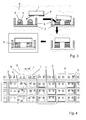
- Figure 1 shows the basic concept of a method of self-assembly including self-alignment of components 1 on a substrate 2 on the basis of surface tension of liquid solder.
- the method involves a solder stack composed of an outermost layer of solder 3 on top and at least another layer of solder 4, the layers of solder having successively increasing melting points from top to bottom.
- the method comprises the following steps: In a first step the solder stack is heated to a temperature between the melting point of the outermost layer of solder 3 and the at least another layer of solder 4. This corresponds to the situation shown in figure 1 in the upper left corner.
- the outermost layer 3 is molten; due to the surface tension the molten solder has a convex shape on its surface towards its environment since it tries to minimize its surface free energy.
- the molten outermost layer 3 is then used to form a receptor which adheres to the components 1 as shown in the upper right corner of figure 1 . Since the molten solder tends to minimize its surface, when a component 1 is adhered to the solder, this will result in the self-assembly, self-alignment and attachment of the components 1.
- Melting of solder is achieved in a liquid environment, the liquid being heated but having a boiling point well above the melting point of the solder used in the outermost layer 3.
- the components 1 therefore are dispensed in a first fluid 6 which is also shown in the first three steps displayed in figure 1 .
- the first fluid 6 is being heated to a temperature below its boiling point but above the melting point of the outermost layer of solder 3.
- This layer of solder 3 then forms a selective adhesive to capture the components 1 as shown in the upper right corner of figure 1 .
- this step can for example be performed in a second fluid at a temperature above the boiling point of the first fluid, or in a gaseous environment like nitrogen or argon, as shown in figure 1 .
- This method overcomes the problem of prior solder directed self-assembly processes that used a single solder layer leading to an interconnect that had a melting point that was limited to be smaller than the boiling point of the first fluid 6 and where no reliable interconnects could be made which would withstand the higher operating temperatures of the assembled devices as they often occur in microdevices. It describes a two-face solder-based receptor to enable high temperature operation of self-assembled objects. However, this aspect is limited to the field of surface tension directed self-assembly on the basis of liquid solder. It extends the allowed operating temperature of current assemblies produced using prior art in the field of solder directed self-assembly which is somewhere in the range of 40-100°C to well above 200°C.
- the new kind of solder based receptor is composed of at least two different solder layers.
- the outermost layer of solder 3 is composed of a low melting point metal alloy and the at least another layer of solder 4 is composed of a higher melting point metal alloy.
- the first step is carried out at low temperature where the low melting point section of the receptor is molten.
- Examples for low melting point alloys are various combinations of the element In, Bi, Sn, Zn, Cd, and Pb in different combination and ratios.
- RoHS Hazardous Substances Directive
- lead and cadmium free solder alloys are also available.
- Different melting points of the solder can be realised using different alloys, for instance a melting point (MP) of 29.8° using 100% Ga, a MP of 47°C using an alloy of ⁇ 44.7%Bi, 22.6% Pb, 19.1% In, 8.3% Sn, 5.3 % Cd ⁇ , a MP of 58°C using ⁇ 49% Bi, 18% Pb, 12% Sn, 21% In ⁇ , a MP of 60°C using ⁇ 51% In 32.5% Bi 16.5% Sn ⁇ , a MP of 69°C using ⁇ 49% Bi, 18% Pb, 18% In, 15% Sn ⁇ , a MP of 79°C using ⁇ 57% Bi, 26% In, 17% Sn ⁇ , a MP of 72 °C using ⁇ 66.3% In, 33.7% Bi ⁇ , a MP of 79°C using ⁇ 57% Bi, 26% In, 17% Sn ⁇ , a MP of 95°C using ⁇ 52.5% Bi, 32% Pb, 15.5% Sn
- the first self-assembly step can and should therefore still be performed in a liquid environment at a modest temperature.
- the first fluid 6 can be water, ethylene glycol or oil.
- the second self-assembly step is a higher temperature reflow step which can be performed in a liquid having a higher boiling point than the first fluid, for example various oil, or inorganic and organic solvents can be used. It also can be performed in a gaseous environment like in air, nitrogen or argon. The temperature is raised to reflow both layers. The reflow step completes the self-assembly and final self-alignment while producing a reliable interconnect with increased melting point.
- the higher melting point solder layer can therefore be composed of a large variety of metallic alloys commonly also used in the electronics industry. Examples include alloys composed of Sn, Ag, Cu in different compositions (so-called SAC solder alloys), and Au.
- an alloy composed of 93.6% Sn, 4.7% Ag, and 1.7% Cu has a melting point of 217°C
- a metal alloy composed of 80% Au, and 20% Sn has a melting point of 280°C.
- solder paste SAC305 composed of 96.5% Sn, 3.0% Ag, and 0.5% Cu is used.
- the previously mentioned materials are only a few examples.
- the industry uses at least 40 different solder compositions and the list of possible combinations is extensive. While figure 1 shows similar thickness for the two solder layers 3 and 4, it is clear that the thickness of the respective layers can be adjusted to tune the melting point and composition of the mixed phase that is formed after reflow.
- the thickness of the at least another layer of solder 4 should be higher than that of the outermost layer of solder 3.
- the composition of the final solder can be tuned to achieve a desired melting point or physical property by selecting a composition of the first solder and thickness and a composition of the second solder and thickness.
- This new type of self-assembly process allows to use a solder stack to form reliable and resilient electrical or mechanical connections, either single or multiple, between the components 1 and the substrate 2, the components 1 being for example semiconductor chips, dies, LED for solid state lighting, RFID-tags, and/or even mechanical parts.
- the substrate 2 has multiple receptor sites mounted on a conveyor belt.
- An example is shown in figure 2 , with a substrate 2 on a conveyor belt 7 moving from left to right through the respective temperature regions. Displayed are four zones, marked by the small curved double lines dividing the conveyor belt 7 and the substrate 2, respectively, in different regions.
- the first region on the left is used to melt the outermost layer of solder 3 which drives the self-assembly of the components 1 into a stable and self-aligned position in the next region. This step takes place in the first fluid 6, while the outermost layer of solder 3 is molten before entering the first fluid 6.
- the components 1 When the components 1 are self-aligned and fixed at their positions, they enter a third region where they can be inspected for example, either manually or by an automatic process using image processing, the latter being the process of choice since the solder stack is repeatedly arranged over an extended surface area and comprises a large number of receptor sites.
- the next step shown in a fourth region on the right side of figure 2 corresponds to the high temperature reflow step of the entire solder stack to form an interconnecting alloy with sufficiently high melting point to ensure operation in real world electronic applications.
- the substrate 2 can also be mounted on a web; it is also possible that the web itself forms the substrate 2.
- pedestals 8 are used on the substrate 2 in combination with the solder stack to define docking sites to assemble components 1 onto the surface of the substrate 2 with unique angular rotation and/or contact pad registration.
- the components 1 displayed in figure 3 have two metal contacts 9, they therefore have to be aligned with correct orientation on the substrate to ensure their function.
- pedestals 8 are used which divide the substrate into different regions. This embodiment is in particular advantageous when used together with a conveyor belt 7 as shown in figure 4 , or webs.
- the components 1 are displayed in a transparent manner to make to contact pads on the surface of the substrate 2 and on the components 1 visible. The process easily can be extended to more than two connections.
- Another aspect is related to avoiding shear forces as they occur in self-assembly methods according to the state of the art as described for example in US 5,545,291 and US 7,774,929 and mentioned in detail in the beginning.
- Scaling the self-assembly mechanism to larger areas is more challenging in the case where protruding objects have to be assembled, since the protruding objects are exposed to additional shear forces.
- protruding objects interfere with the component delivery mechanism which has been done using a slurry of self-assembly components that slides a long the surface to populate receptor sites.
- a large number of components 1 with metal contacts 9 is shown in a liquid environment 10 as they slide along an inclined surface of a substrate 2.
- receptor sites 11 are arranged on the substrate 2. Due to the large number of components, on some of the components already adhered to the selective adhesive element, massive shear forces are exerted as demonstrated at shear points 12, resulting in a lateral shift of already assembled components 1 which might in the worst case lead to removal of those components 1 or in an alignment which is not correct.
- This difficulty can be overcome applying a fluidic self-assembly method of a plurality of components 1 onto receptor sites 11 on the surface of a substrate 2, where each receptor site 11 is formed of a selective adhesive which adheres to at least a part of the components 1 resulting in the capture, self-alignment and/or attachment of the components 1 at the receptor sites 11.
- the selective adhesive element might be a simple solder junction, a simple hydrophobic adhesive or also a solder stack, to list only a few examples.
- the substrate 2 with the receptor site 11 is transported in an essentially upright position at a predetermined speed into a delivery zone, the zone comprising a fluid 13.
- the speed may be chosen in a range between 1 cm/min and 100cm/min, but eventually larger speed can be applied as technology advances.
- the components 1 are dispensed into the fluid 13 by a dispensing unit located above the delivery zone, resulting in a portion of components 1 getting attached to receptor sites 11 and a remaining portion of components 1 forming excess components not attached to receptor sites 11.
- "Essentially upright" means that in the delivery zone the substrate and the receptor site 11 on it are aligned to a horizontal plane in a way that components 1 getting adhered will not slide down due to gravity.
- the expression "essentially upright” therefore also includes planes with an inclination angle where this condition is fulfilled.
- the inclination angle depends on the liquid and on the density of the components; it might for example take values in a range up to 55° for slow moving substrates and up to 75° in cases where the substrate velocity is increased.
- the substrate 2 is transported out of the delivery zone and rotated into a position where the receptor sites 11 take an essentially upside-down position, thereby forcing excess components stuck at the surface of the substrate 2 to drop off it and to sink to a lower region.
- the expression "essentially upside-down” includes a large variety of angles of inclination apart from the horizontal plane at which excess components drop off the substrate 2.
- the inclination angle might be ⁇ 45° for example.
- Excess components are collected at at least one collecting point at the bottom of the lower region and transported back to the dispensing unit through at least one pathway. Then they are reused.
- Speed and optionally the angle of inclination are adjusted dependent on the properties of the fluid 13 and of the components 1 to minimize the force exerted by excess components onto already assembled components 1.
- the substrate might be vibrated or a liquid jet might be directed onto the surface of the substrate 2, using the fluid 13. Vibration and jet can also be applied together.
- Figure 6 shows the basic concept of an apparatus which can be used for performing the method described above, i.e. for self-assembly of components 1 onto receptor sites 11 of the surface of a substrate 2, where each receptor site 11 is formed of a selective adhesive element which adheres to at least a part of the components 1 resulting in the capture, self-assembly, self-alignment and/or attachment of the components 1 at the receptor sites 11.
- the apparatus shown in figure 1 comprises a basin 14 containing a fluid 13.
- the apparatus further comprises first transporting means for transporting the substrate 2 with the receptor sites 11 in an essential upright position at a predetermined speed and/or angle of inclination into and out of a delivery zone 16 in the fluid 13.
- a dispensing unit 17 is located which is used for dispensing components 1 into the fluid 13 and onto the substrate 2.
- the apparatus further comprises rotating means for rotating the substrate 2 into a position where the receptor sites 11 take an essentially upside-down position.
- the apparatus also comprises collecting means for collecting excess components 18 not attached to receptor sites 11 at the bottom of the basin 14, and second transporting means for returning excess components 18 to the dispensing unit 17.
- the first transporting means comprise a uniform prism shaped rod 15 which is composed of several flat elements resulting in a rod 15 with a polygonal cross section.
- the cross section corresponds to a hexagon, but shapes of other regular polygons or even of a circular cross section are also applicable.
- larger flat areas have the advantage that predetermined speed and/or optional an inclination angle can be kept over a longer distance and/or time respectively.
- the rotating means form an integrated part of the first transporting means; the rod 15 is rotated about its axis of symmetry. Components 1 are dropped from above by the dispensing unit 17 into the basin 14. Due to the rotation of rod 15, a flow is induced in the fluid 13 resulting in a drift of the components 1 after having entered basin 14.
- the dispensing unit 8 can be located above the surface of fluid 13, but its outlet can also be located below the surface level of fluid 13.
- the connecting means include at least a funnel 19 for connecting the excess components 18, the exit 10 of funnel 19 being connected to the second transporting means.
- the components 1 are getting attached to receptor sites 11 when in a region 21.
- the drift of components 1 which is directed in the figure to the left and downwards corresponds to the angle of inclination of the substrate 2 currently in that region 21 and to its current tangential velocity in region 21.
- the rotating speed of the rod 15 preferably is adapted to minimize the shear force that is exerted by excess components 18 ⁇ which are for example chips or dies ⁇ onto already assembled components 1.
- the direction of sedimentation and capture of the excess components 18 is achieved using inclined planes which are forming the walls of the funnel 19.
- Other collecting means comprising inclined planes not in the shape of a funnel, but for example in the form of a "V" or else, might also be used.
- the sedimentation is driven by gravity and not liquid motion or drag forces. In other words there is no need for liquid flow, which would result in excessive flow rates in the confined collection points.
- this collection process is limited to components 1 that have a higher density than the surrounding liquid.
- the inclination angle of the funnel 19 or the inclined planes might and should be adapted according to the density or mass of the components 1 in relation to the density of liquid 13.
- the angle of inclination should exceed 30° to avoid undesired non-specific adhesion of objects at the inclined surfaces.
- both sliding motion and shear forces can be adjusted to be essentially zero by adjusting the velocity of the forward motion of the substrate and optionally adjusting the inclination angle.
- the upside-down removal of excess components 18 uses gravity, but can be assisted with or without liquid jet, the latter for example produced by a pump 22.
- Successive passes underneath of the dispensing elements in combination with intermediate upside-down orientation of the self-assembly substrate increases the self-assembly yield which is measured by the number of receptor sites 11 that have captured a component 1. Particular in cases where the pitch of the assembly is only slightly larger than the component size several passes are required to achieve yields approaching 100%.
- the reason for the appearance of defects is that a fraction of the receptors get obstructed with components 1 that are not oriented correctly for the self-assembly to take place. Affected receptors and regions with non-specific adhesion get cleaned as the effected substrate is rotated to the essentially upside-down position. Successive passes complete the self-assembly.
- Figure 7 shows a similar apparatus as in figure 6 , the difference being mainly that instead of rod 15, a conveyor belt 7 is used. This makes it possible to keep the angle of inclination for the substrate 2 over a longer distance, i.e. the substrate can be kept longer in the essentially upright or essentially upside-down position which makes attachment and removal more efficient and controllable.
- a conveyor belt 7 instead of a conveyor belt 7, also a web could be used.
- the rotating means are preferably an integrated part of the first transporting means and located at the reversal point for the movement of the conveyor belt or of the web, respectively.
- a pump 23 can be used which is shown here in a pathway 24 connecting the exit of the funnel 20 with the dispensing unit 17. The pump 23 is used to pump excess components 18 collected in the funnel 19 from the exit of the funnel 20 to the dispensing unit 17.
- Figure 8 shows a combination of two of such apparatus, which are connected only by the conveyor belt 7.
- Such an arrangement might for example be used to assemble different components on the substrate 2.
- the substrate might comprise different receptor sites, a portion of them being selectively adhesive only for components in the left apparatus and the other portion being selectively adhesive only for components in the apparatus on the right side of figure 8 .
- the arrangement of fig. 8 might also be used to improve efficiency by using the same type of components in both apparatus.
- a web can be used instead of a conveyor belt 7 a web can be used.
- conveyor belts 7 While usually conveyor belts 7 are rotated and reversed in their direction of motion around an axis perpendicular to the direction of transport, and while this also is standard for webs, the latter can also be rotated around a rotation axis which is parallel to the direction of transport as shown in figure 9 .
- each collection region is connected to a separate funnel, the widths and throughput of the assembly apparatus is increased repeating this design to accommodate increasingly wide webs.
- a linear funnel array 27 is integrated in the apparatus below the turning point at the web 25 or at the reversal point of a tilted conveyor belt.
- the depicted collection and re-circulation module shows six parallel funnels. The dimensions of the collection block are reduced; the thickness behaves roughly inversely linear to the number of funnels in the linear array 27.
- the overall funnel volume will be reduced by a factor of 100.
- the Z-shaped receptor pattern is only an example which is kept simple for clarity.
- the preferred receptor pattern is a regular array to distribute LED light sources over increasingly large webs or substrates at a desired pitch leading to an electrically interconnected pattern where the substrate provides the electrical connections to the LEDs.
- the dispensing unit 17 comprises several inlet openings, the number of inlet openings preferably corresponding to the number of collecting points where each inlet opening is connected by a separate pathway 24 to at least one collecting point.
- This particular embodiment is shown in figure 11 .
- the array of collection points is connected with several parallel channels to transport the self-assembly components upwards before they are introduced at the surface of the self-assembly substrate again.
- the order of collecting points might also be changed if the apparatus itself has a somewhat tilted orientation leading to the situation that for example at the leftmost collecting point more excess components 18 are collected then at the rightmost collecting point, considered from the direction of transport. In that case, the pathway 24 from the leftmost collecting point could be connected to the rightmost inlet opening of the dispensing unit 17.
- the pumping means as being part of the second transporting means include at least one jet pump 28 for generating a jet of liquid. Excess components 18 are collected by the funnel 19 at its exit 20 on the basis of gravity.
- FIG. 12a Transport of the self-assembly components 1 to higher altitudes and remote locations including the self-assembly substrate 2 is achieved using a jet pump principle which in figure 12a ) includes a three-way terminal junction with a reduced junction on one side, the jet pump 28 preferably being equipped with a Venturi nozzle or an orifice plate.
- the jet leads to a liquid circulation though the pathways 24 which transport the excess components 18 due to the drag force to remote points.
- the excess components 18 do not pass though a mechanical pump with moving parts and are not damaged as a result.
- Figure 12a shows the preferred embodiment.
- Clogs at the exit location that form once the system is turned off can be cleared using a valve in pathway 24 that turns off pathway 24 diverting the liquid flow upward at exit 20 which disassembles the clog dispersing the components above the funnel region.
- the jet pump 28 is located along the pathway 24 at some higher altitude.
- this alternative has also a disadvantage in that it leads to additional downward liquid flow at exit 20 which might damage the components 1. It is also not effective in removing clogs.
- a fluid current produced due to reduced pressure at the exit 20 of the funnel such that excess components 18 are transported away through pathway 24 during steady state operation without having an excessive flow rate at junction points which could damage components 1.
- the embodiments shown in figures 12a) and 12b ) might also be combined with each other, further it might also be advantageous to use another jet pump to direct an upward jet into the funnel region to remove clogs which may occur due to excessive collection of excess components 18.
- the concept of using a jet pump 28 might in particular also be combined with the linear funnel array 27, as shown in figure 13 .
- the basic building unit 30 is shown at the bottom right and is repeated to increase the width of the collection unit while maintaining the same cross section
- the manifold 31 distributes the incoming pressurized fluid to produce n liquid jets due to the reduced diameter port opening 33 and/or orifice plate.
- Excess components 18 are collected by the funnel 19 at its exit on the basis of gravity.
- the particular design minimizes liquid flow in this region. No downward liquid is required and components tumble down on the basis of gravity. A downward liquid flow produces additional shear forces which are prevented.
- the directed jet transports the excess components 18 away to the left and subsequently through pathways 24 which transport the excess components 18 back to the dispensing unit.
Landscapes
- Engineering & Computer Science (AREA)
- Mechanical Engineering (AREA)
- Microelectronics & Electronic Packaging (AREA)
- Computer Hardware Design (AREA)
- Power Engineering (AREA)
- Manufacturing & Machinery (AREA)
- Physics & Mathematics (AREA)
- Condensed Matter Physics & Semiconductors (AREA)
- General Physics & Mathematics (AREA)
- Electric Connection Of Electric Components To Printed Circuits (AREA)
Abstract
Description
- The invention relates to a method of self-assembly including self-alignment of components on a substrate on the basis of surface tension of liquid solder for applications that require reliable operation of the self-assembled objects at elevated operation temperatures. It also relates to a method and an apparatus of fluidic self-assembly of a plurality of components onto receptor sites on the surface of a substrate, where each receptor site is formed of a selective adhesive which adheres to at least a part of the components resulting in the capture, self-alignment and/or attachment of the components at the receptor sites, integrating component delivery, removal, and attachment over increasingly large surfaces.
- The construction of almost all man-made artifacts such as packaged LEDs, solid state lighting panels, cell phones, or computers relies on robotic assembly lines that place, package, and interconnect a variety of devices that have microscopic dimensions, i.e. with dimensions smaller than 1 mm. The key to the realization of these devices and systems is our ability to integrate/assemble components as well as to link/interconnect the components to transport energy and information. The tools of choice in the established manufacturing industry are robotic pick and place machines and wire bonding concepts. Conventional robotic methods, however, are challenged because of the difficulty in building machines that can economically manipulate and interconnect microscopic parts over large areas with high throughput. At the other extreme, nature forms materials, structures, and living systems by self-assembly on a molecular length scale. As a result self-assembly based fabrication strategies are widely recognized as inevitable tools in nanotechnology. However, self-assembly is not limited to the nanometer length scale. Strategies based on self-assembly are projected to have a major impact in the future manufacturing of macroscopic systems ― with dimensions larger than 1 mm ― that use microscopic building blocks.
- In
US 5,545921 andUS 6,780,696 a process is described to direct the assembly of small radio frequency identification (RFID) tags. Semiconductor chips are suspended in a liquid flow over a surface containing correspondingly shaped wells that act as receptors for the device components. The device components settle into these wells due to gravitational forces. - The process has the advantage that it produces a flat surface. Assembled components fill the wells and form a flush surface. Subsequent components slide over already assembled objects and there is little interference. This particular process has the advantage the self-assembled objects are not protruding. Scaling to large areas and continuous assembly on webs having widths of more than 10 cm has been possible with little effort in terms of the machine design. This process requires very specific die geometries ― L or T shaped blocks for angular orientation and trapezoids to prevent up-side down assembly ― these particular shapes are not common in the microelectronics industry; most dies are square in shape. While they remain valid solutions they limit wide spread use. Attempts of adoption by other manufacturers remain critically low because of the required use of trapezoidal chips that are not widely used. A more universal solution is desired and would increase the chance of technology adoption and transition.
- An advantage of all self-assembly processes is that they are massively parallel, which potentially reduces the assembly costs dramatically relative to the costs of traditional deterministic pick and place methods that use serial robotic methods.
- In the publication " Self-assembly at all scales" from Whitesides et al., published in Science 295, p. 2418-2421 (2002), the use of surface tension to self-assemble components that are freely suspended in a liquid was described. In the publication "Self-assembly of mesoscale objects into ordered two-dimensional arrays" of Bowden et al., published in Science 276, p. 322-325 (1997), the self-assembly of components having a size of 5 mm with patterned hydrophobic surfaces into ordered aggregates has been described.
- The concept of solder directed self-assembly is for example described and applied in
US 7,774,929 . The components self-assemble and attach to the solder-coated areas due to the reduction of the surface free energy of the liquid solder surface. The method has been applied to direct the assembly of chip-sized components onto surfaces from a heated suspension primarily in the context of solid state lighting, photovoltaic, and multicomponent sensors. One of the mechanisms of self-assembly and attachment of the chips is based on surface tension directed self-assembly on the basis of liquid solder. The self-assembly process is driven by the minimization of surface free energy of the liquid solder. A difference here when compared to the prior art on surface tension directed self-assembly at the time was that the solder was placed only on the receiving substrate to form a selective adhesive element for metal contacts on conventional semiconductor chips. The randomly moving self-assembly semiconductor chips themselves did not have a solder bump on their surface. In the particular design, the metal contact on the component binds to the liquid-solder-based-receptors during the self-assembly process at a temperature where the solder is molten. The solder wets the metal contact during the process and the minimization of the free surface area of the liquid solder drives the assembly into a stable, aligned position. The parallel assembly of large number of components has been accomplished using this process. The liquid-solder-coated areas act as receptors for subunits during the assembly ― no manipulator is needed ―, they form rigid bonds upon solidification ― no adhesive is needed ―, and provide electrical input/output-connectors to operate the final device ― no wire bonder is needed. - Solder directed fluidic self-assembly as it has been described today is done inside a closed vial, barrel, or container to suspend the self-assembly components in a fluid at a temperature where the solder is molten.
- A major limitation of solder directed self-assembly as it is known today is the fact that the melting point of the solder has to be below the boiling point of the fluid that is used in the fluidic self-assembly process. For example often water is used as a fluid which limits the melting point of the solder to be below 100°C. To assemble devices then mostly solder is used that has a melting point below 60°C. While it is possible to replace the water with ethylene glycol or other higher boiling point liquids, it has not yet been possible to form reliable interconnects using this approach. It appears that there are no solvents that support the self-assembly at sufficiently high temperatures that would work with the same solder based interconnects that are used in the electronics industry. This is the main reason why solder directed self-assembly has not been used in an industrial process today.
- On the other hand, in the more established field of deterministic robotic flip chip assembly and packaging of semiconductor components sometimes a solder stack is used that is composed of two solder layers that have different compositions and thus different melting points. In this field the objects are always brought into contact using micromanipulators, referred to as deterministic rather than stochastic assembly.
- In
TW 517370 B - Another example is described in
US 5,872,400 . There, solder balls are disclosed that have high melting point cores which are partially or completely coated with a lower melting point solder. The balls are applied in a ball grid array (BGA) and the particular process allows for a tighter control of the ball dimensions which in turn allows for higher interconnect density in surface mount packaging without bridging. - Another example is described in
US 6,340,630 . Again the layered system is used in the application field of BGA. The application describes transfer of solder bumps from a mold leading to BGA connection on a wafer that have a dual metallurgical composition after reflow. - Another example is described in
WO 96/16442 - Another problem is that self-assembled chips and objects are not generally flush with the surrounding surface. To get a flush surface it is required to use particular die shapes such as trapezoidal shaped dies as in
US 5,545,291 which are not very common in the industry. A more common die shape is based on rectangular square shaped blocks. These can be self-assembled onto receptors using selective adhesive elements of which liquid solder is the element of choice since it likes to wet certain metals which results into the capture of chips with metal contacts. From an application point of view this is an advantage since it is less restrictive on the components and shapes that can be assembled. However, scaling to large areas is more challenging since protruding objects interfere with the component delivery mechanism which has been done using a slurry of self-assembly components that slides along the surface to populate receptor sides. - Examples of prior implementations are described in
US 5,545,291 andUS 7,774,929 . The first document describes the use of a slurry of components that slides across a planar surface. The components drop into the recessed openings on the basis of gravity and shape recognition. The second document describes the use of a closed rotating barrel that holds the self-assembly substrate. The substrate is attached inside the barrel and points towards the center of the barrel. The barrel itself holds the self-assembly objects. Back-and-forth partial rotation of the barrel leads to a successive sweeping motion of self-assembly components that slide over the surface and that interact with the receptors. Both solutions work perfectly well using trapezoidal shaped dies, the process described inUS 7,774,929 is also applied to semiconductor chips and shapes that include rectangular blocks which are more common in industry. However, both solutions have in common that they cause shear forces in cases of self-assembled objects that are not flush with the surrounding surface. The collective movement of excess self-assembly components causes a shear force on already assembled objects which becomes increasingly difficult to manage if a large number of excess components is present in the system. Self-assembled objects are often raised features which are not flush with the intermediate surrounding surface. The shear force becomes increasingly difficult to manage if large volumes of excess components slide across the surface which is required in cases where the substrate size is increased. Large area assembly of objects that are raised above the receiving surface has not been possible using a simple system like the barrel design. Published results regarding the substrate size have been smaller than 2 cm2 in cases where the objects were raised features. - First object of the invention is to enhance a self-assembly method based on solder in a way that also microelectronic components which have to withstand higher temperatures than currently achievable can be produced by using a self-assembly process as described in the beginning. Another object of the invention is to enhance a method of and to develop an apparatus for self-assembly of a plurality of components onto receptor sites on a surface of a substrate where the receptor sites are formed of selective adhesives and in particular to reduce shear forces caused by protruding elements to a minimum to allow the assembly of larger numbers of protruding components than currently possible. In combination, self-assembly of large numbers of protruding components over wide areas substrates forming reliable interconnects should be achieved.
- The first problem is solved by a method as described in
claim 1. The second problem is solved by a method as described inclaim 6 and an apparatus as described inclaim 12. Preferred and advantageous embodiments of the methods and the apparatus are described in the dependent claims. - It is understood that the features mentioned before and in particular in the claims, and the features to be explained below are applicable not only in the combination stated but also in other combinations or as standalone features without leaving the scope of the present invention.
- Below, the invention will be explained in more detail with reference to the accompanying drawings, which also show features essential to the invention, among others, and in which
- Fig. 1
- shows the principle of a self-assembly method using a solder stack,
- Fig. 2
- shows an implementation using a conveyor belt,
- Fig. 3
- shows another implementation of the method using pedestals,
- Fig. 4
- shows the implementation of
Fig. 3 using a conveyer belt. - Fig. 5
- shows shear forces occurring in prior art apparatus,
- Fig. 6
- shows a first example for an apparatus for self assembly
- Fig. 7
- shows a second example for an apparatus for self-assembly using a conveyor belt
- Fig. 8
- shows a third example of an apparatus for self-assembly with two units successively coupled,
- Fig. 9
- shows a fourth example of an apparatus for self-assembly based on a web,
- Fig. 10 a, b)
- shows examples for collecting means for components to be reused,
- Fig. 11
- shows an example for arranging pathways where the excess components are transported,
- Fig. 12 a, b)
- shows two ways for pumping excess components to be reused, and
- Fig. 13
- shows a combination of a collection point array equipped with jet pumps.
-
Figure 1 shows the basic concept of a method of self-assembly including self-alignment ofcomponents 1 on asubstrate 2 on the basis of surface tension of liquid solder. The method involves a solder stack composed of an outermost layer ofsolder 3 on top and at least another layer ofsolder 4, the layers of solder having successively increasing melting points from top to bottom. - The method comprises the following steps: In a first step the solder stack is heated to a temperature between the melting point of the outermost layer of
solder 3 and the at least another layer ofsolder 4. This corresponds to the situation shown infigure 1 in the upper left corner. Theoutermost layer 3 is molten; due to the surface tension the molten solder has a convex shape on its surface towards its environment since it tries to minimize its surface free energy. The moltenoutermost layer 3 is then used to form a receptor which adheres to thecomponents 1 as shown in the upper right corner offigure 1 . Since the molten solder tends to minimize its surface, when acomponent 1 is adhered to the solder, this will result in the self-assembly, self-alignment and attachment of thecomponents 1. This situation is shown in the lower right corner offigure 1 . The outermost layer ofsolder 3 is still molten. In the next step the solder stack is heated to a temperature above the melting point of the at least another layer ofsolder 4. This initialises a reflow soldering-process of the outermost and the at least another layer ofsolder alloy 5 to form an interconnect between the components and the substrate with a melting point higher than that of the outermost layer ofsolder 3. This situation is shown in the lower left corner offigure 1 . - Melting of solder is achieved in a liquid environment, the liquid being heated but having a boiling point well above the melting point of the solder used in the
outermost layer 3. In an advantageous embodiment thecomponents 1 therefore are dispensed in afirst fluid 6 which is also shown in the first three steps displayed infigure 1 . Thefirst fluid 6 is being heated to a temperature below its boiling point but above the melting point of the outermost layer ofsolder 3. This layer ofsolder 3 then forms a selective adhesive to capture thecomponents 1 as shown in the upper right corner offigure 1 . - To heat the at least another layer of
solder 4 to a temperature above its melting point this environment has to be changed which is why the last step of the method displayed in the lower left corner offigure 1 is shown in a box. This step can for example be performed in a second fluid at a temperature above the boiling point of the first fluid, or in a gaseous environment like nitrogen or argon, as shown infigure 1 . - This method overcomes the problem of prior solder directed self-assembly processes that used a single solder layer leading to an interconnect that had a melting point that was limited to be smaller than the boiling point of the
first fluid 6 and where no reliable interconnects could be made which would withstand the higher operating temperatures of the assembled devices as they often occur in microdevices. It describes a two-face solder-based receptor to enable high temperature operation of self-assembled objects. However, this aspect is limited to the field of surface tension directed self-assembly on the basis of liquid solder. It extends the allowed operating temperature of current assemblies produced using prior art in the field of solder directed self-assembly which is somewhere in the range of 40-100°C to well above 200°C. The new kind of solder based receptor is composed of at least two different solder layers. The outermost layer ofsolder 3 is composed of a low melting point metal alloy and the at least another layer ofsolder 4 is composed of a higher melting point metal alloy. Using this new type of receptor the self-assembly process is divided into the aforementioned two-step sequence. The first step is carried out at low temperature where the low melting point section of the receptor is molten. Examples for low melting point alloys are various combinations of the element In, Bi, Sn, Zn, Cd, and Pb in different combination and ratios. To fulfil the Restriction of Hazardous Substances Directive (RoHS), lead and cadmium free solder alloys are also available. Different melting points of the solder can be realised using different alloys, for instance a melting point (MP) of 29.8° using 100% Ga, a MP of 47°C using an alloy of {44.7%Bi, 22.6% Pb, 19.1% In, 8.3% Sn, 5.3 % Cd}, a MP of 58°C using {49% Bi, 18% Pb, 12% Sn, 21% In}, a MP of 60°C using {51% In 32.5% Bi 16.5% Sn}, a MP of 69°C using {49% Bi, 18% Pb, 18% In, 15% Sn}, a MP of 79°C using {57% Bi, 26% In, 17% Sn}, a MP of 72 °C using {66.3% In, 33.7% Bi}, a MP of 79°C using {57% Bi, 26% In, 17% Sn}, a MP of 95°C using {52.5% Bi, 32% Pb, 15.5% Sn}, a MP of 103 °C using {54% Bi, 26% Sn, 20% Cd}, a MP of 108°C using { 52.2% In, 46% Sn, 1.8% Zn}, a MP of 118°C using {58% Sn, 42% In} or {50% Sn, 50% In}, a MP of 138°C using {57% Bi, 43% Sn}. These metal alloys work well due to high surface tension and fast wetting characteristic attaching to the metal contacts of thecomponents 1. The first self-assembly step can and should therefore still be performed in a liquid environment at a modest temperature. For example, thefirst fluid 6 can be water, ethylene glycol or oil. - The second self-assembly step is a higher temperature reflow step which can be performed in a liquid having a higher boiling point than the first fluid, for example various oil, or inorganic and organic solvents can be used. It also can be performed in a gaseous environment like in air, nitrogen or argon. The temperature is raised to reflow both layers. The reflow step completes the self-assembly and final self-alignment while producing a reliable interconnect with increased melting point. The higher melting point solder layer can therefore be composed of a large variety of metallic alloys commonly also used in the electronics industry. Examples include alloys composed of Sn, Ag, Cu in different compositions (so-called SAC solder alloys), and Au. For example, an alloy composed of 93.6% Sn, 4.7% Ag, and 1.7% Cu has a melting point of 217°C, and a metal alloy composed of 80% Au, and 20% Sn has a melting point of 280°C. For instance, for packaging of power LED, solder paste SAC305 composed of 96.5% Sn, 3.0% Ag, and 0.5% Cu is used. The previously mentioned materials are only a few examples. The industry uses at least 40 different solder compositions and the list of possible combinations is extensive. While
figure 1 shows similar thickness for the twosolder layers solder 4 should be higher than that of the outermost layer ofsolder 3. The composition of the final solder can be tuned to achieve a desired melting point or physical property by selecting a composition of the first solder and thickness and a composition of the second solder and thickness. - This new type of self-assembly process allows to use a solder stack to form reliable and resilient electrical or mechanical connections, either single or multiple, between the
components 1 and thesubstrate 2, thecomponents 1 being for example semiconductor chips, dies, LED for solid state lighting, RFID-tags, and/or even mechanical parts. - In an advantageous embodiment to enable assembly in large volumes, the
substrate 2 has multiple receptor sites mounted on a conveyor belt. An example is shown infigure 2 , with asubstrate 2 on aconveyor belt 7 moving from left to right through the respective temperature regions. Displayed are four zones, marked by the small curved double lines dividing theconveyor belt 7 and thesubstrate 2, respectively, in different regions. The first region on the left is used to melt the outermost layer ofsolder 3 which drives the self-assembly of thecomponents 1 into a stable and self-aligned position in the next region. This step takes place in thefirst fluid 6, while the outermost layer ofsolder 3 is molten before entering thefirst fluid 6. When thecomponents 1 are self-aligned and fixed at their positions, they enter a third region where they can be inspected for example, either manually or by an automatic process using image processing, the latter being the process of choice since the solder stack is repeatedly arranged over an extended surface area and comprises a large number of receptor sites. The next step shown in a fourth region on the right side offigure 2 corresponds to the high temperature reflow step of the entire solder stack to form an interconnecting alloy with sufficiently high melting point to ensure operation in real world electronic applications. - Instead of mounting the
substrate 2 on aconveyor belt 7, thesubstrate 2 can also be mounted on a web; it is also possible that the web itself forms thesubstrate 2. - Referring now to
figure 3 , in another advantageous embodiment pedestals 8 are used on thesubstrate 2 in combination with the solder stack to define docking sites to assemblecomponents 1 onto the surface of thesubstrate 2 with unique angular rotation and/or contact pad registration. Instead of having only onemetal contact 9 like thecomponents 1 shown infigure 1 , thecomponents 1 displayed infigure 3 have twometal contacts 9, they therefore have to be aligned with correct orientation on the substrate to ensure their function. To achieve correct orientation and electrical connections of thecomponents 1 as an integral part of the self-assembly process using the solder stacks, pedestals 8 are used which divide the substrate into different regions. This embodiment is in particular advantageous when used together with aconveyor belt 7 as shown infigure 4 , or webs. Infigure 4 , thecomponents 1 are displayed in a transparent manner to make to contact pads on the surface of thesubstrate 2 and on thecomponents 1 visible. The process easily can be extended to more than two connections. - Another aspect is related to avoiding shear forces as they occur in self-assembly methods according to the state of the art as described for example in
US 5,545,291 andUS 7,774,929 and mentioned in detail in the beginning. Scaling the self-assembly mechanism to larger areas, however, is more challenging in the case where protruding objects have to be assembled, since the protruding objects are exposed to additional shear forces. In particular protruding objects interfere with the component delivery mechanism which has been done using a slurry of self-assembly components that slides a long the surface to populate receptor sites. Assembly yields exceeding 99% using the mechanism of surface tension driven self-assembly as described inUS 7,774,929 has only been achieved using a closed barrel design where the self-assembly substrate is attached inside the barrel and where the self-assembly surface points to the centre of the barrel, and where the inside of the barrel is filled with a suspension of self-assembly components. The closed barrel design forms a tilted plane where excess self-assembly components slide down to assemble on empty receptors. However, in case where the self-assembled objects are raised features which are not flush with the intermediate surrounding surface the sliding motion of the aggregated component slurry causes a lateral shear force as shown for example infigure 5 . Here, a large number ofcomponents 1 withmetal contacts 9 is shown in a liquid environment 10 as they slide along an inclined surface of asubstrate 2. On thesubstrate 2,receptor sites 11 are arranged. Due to the large number of components, on some of the components already adhered to the selective adhesive element, massive shear forces are exerted as demonstrated atshear points 12, resulting in a lateral shift of already assembledcomponents 1 which might in the worst case lead to removal of thosecomponents 1 or in an alignment which is not correct. - This difficulty can be overcome applying a fluidic self-assembly method of a plurality of
components 1 ontoreceptor sites 11 on the surface of asubstrate 2, where eachreceptor site 11 is formed of a selective adhesive which adheres to at least a part of thecomponents 1 resulting in the capture, self-alignment and/or attachment of thecomponents 1 at thereceptor sites 11. An apparatus for performing this method will be described further below referring tofigure 6 which also serves to exemplify the method steps. The selective adhesive element might be a simple solder junction, a simple hydrophobic adhesive or also a solder stack, to list only a few examples. In a first step in this method thesubstrate 2 with thereceptor site 11 is transported in an essentially upright position at a predetermined speed into a delivery zone, the zone comprising afluid 13. For example, currently the speed may be chosen in a range between 1 cm/min and 100cm/min, but eventually larger speed can be applied as technology advances. Thecomponents 1 are dispensed into the fluid 13 by a dispensing unit located above the delivery zone, resulting in a portion ofcomponents 1 getting attached toreceptor sites 11 and a remaining portion ofcomponents 1 forming excess components not attached toreceptor sites 11. "Essentially upright" means that in the delivery zone the substrate and thereceptor site 11 on it are aligned to a horizontal plane in a way thatcomponents 1 getting adhered will not slide down due to gravity. Apart form a horizontal orientation the expression "essentially upright" therefore also includes planes with an inclination angle where this condition is fulfilled. The inclination angle depends on the liquid and on the density of the components; it might for example take values in a range up to 55° for slow moving substrates and up to 75° in cases where the substrate velocity is increased. - In the next step the
substrate 2 is transported out of the delivery zone and rotated into a position where thereceptor sites 11 take an essentially upside-down position, thereby forcing excess components stuck at the surface of thesubstrate 2 to drop off it and to sink to a lower region. Here again, the expression "essentially upside-down" includes a large variety of angles of inclination apart from the horizontal plane at which excess components drop off thesubstrate 2. The inclination angle might be ― 45° for example. - Excess components are collected at at least one collecting point at the bottom of the lower region and transported back to the dispensing unit through at least one pathway. Then they are reused.
- Speed and optionally the angle of inclination are adjusted dependent on the properties of the fluid 13 and of the
components 1 to minimize the force exerted by excess components onto already assembledcomponents 1. - To support removing excess components remaining on the substrate after rotating it into the essentially upside-down position, the substrate might be vibrated or a liquid jet might be directed onto the surface of the
substrate 2, using thefluid 13. Vibration and jet can also be applied together. -
Figure 6 shows the basic concept of an apparatus which can be used for performing the method described above, i.e. for self-assembly ofcomponents 1 ontoreceptor sites 11 of the surface of asubstrate 2, where eachreceptor site 11 is formed of a selective adhesive element which adheres to at least a part of thecomponents 1 resulting in the capture, self-assembly, self-alignment and/or attachment of thecomponents 1 at thereceptor sites 11. The apparatus shown infigure 1 comprises abasin 14 containing a fluid 13. The apparatus further comprises first transporting means for transporting thesubstrate 2 with thereceptor sites 11 in an essential upright position at a predetermined speed and/or angle of inclination into and out of adelivery zone 16 in thefluid 13. Above the delivery zone 16 adispensing unit 17 is located which is used for dispensingcomponents 1 into the fluid 13 and onto thesubstrate 2. The apparatus further comprises rotating means for rotating thesubstrate 2 into a position where thereceptor sites 11 take an essentially upside-down position. The apparatus also comprises collecting means for collectingexcess components 18 not attached toreceptor sites 11 at the bottom of thebasin 14, and second transporting means for returningexcess components 18 to the dispensingunit 17. - The first transporting means comprise a uniform prism shaped
rod 15 which is composed of several flat elements resulting in arod 15 with a polygonal cross section. In the example shown infigure 1 , the cross section corresponds to a hexagon, but shapes of other regular polygons or even of a circular cross section are also applicable. However, larger flat areas have the advantage that predetermined speed and/or optional an inclination angle can be kept over a longer distance and/or time respectively. The rotating means form an integrated part of the first transporting means; therod 15 is rotated about its axis of symmetry.Components 1 are dropped from above by the dispensingunit 17 into thebasin 14. Due to the rotation ofrod 15, a flow is induced in the fluid 13 resulting in a drift of thecomponents 1 after having enteredbasin 14. The dispensingunit 8 can be located above the surface offluid 13, but its outlet can also be located below the surface level offluid 13. - Located at the bottom of the
basin 14, the connecting means include at least afunnel 19 for connecting theexcess components 18, the exit 10 offunnel 19 being connected to the second transporting means. - As can be seen in
figure 6 , thecomponents 1 are getting attached toreceptor sites 11 when in aregion 21. There, the drift ofcomponents 1 which is directed in the figure to the left and downwards corresponds to the angle of inclination of thesubstrate 2 currently in thatregion 21 and to its current tangential velocity inregion 21. The rotating speed of therod 15 preferably is adapted to minimize the shear force that is exerted byexcess components 18 ― which are for example chips or dies ― onto already assembledcomponents 1. - Shear forces on already self-assembled
components 2 that arise above the surface can be almost completely eliminated momentarily by using this mechanism. When therod 15 is rotating further,excess components 18 stuck to the surface are dropping down from it due to the gravitational force when the substrate takes a position withreceptor sites 11 in an essentially upside-down position. Essentially upside-down and essentially upside in this relation does not mean that the substrate has to be orientated strictly in a horizontal manner, but also includes inclination angles up to at least 45°. -
Excess components 18 which have not been attached toreceptor sites 11, for example due to the fact that at the position where those components reached thesubstrate 2 already acomponent 1 had been attached, or due to a wrong orientation of the component at the point when it reached the surface of thesubstrate 2, are collected at the bottom of thebasin 14 using thefunnel 19. The direction of sedimentation and capture of theexcess components 18 is achieved using inclined planes which are forming the walls of thefunnel 19. Other collecting means comprising inclined planes not in the shape of a funnel, but for example in the form of a "V" or else, might also be used. The sedimentation is driven by gravity and not liquid motion or drag forces. In other words there is no need for liquid flow, which would result in excessive flow rates in the confined collection points. Nevertheless, this collection process is limited tocomponents 1 that have a higher density than the surrounding liquid. The inclination angle of thefunnel 19 or the inclined planes might and should be adapted according to the density or mass of thecomponents 1 in relation to the density ofliquid 13. When for example semi conductor chips composed of silicon with a density of 2.33g/cm3 and of GaN, having a density of 6.15g/cm3 the angle of inclination should exceed 30° to avoid undesired non-specific adhesion of objects at the inclined surfaces. - In such a case there would be a need for additional means to remove
components 1 from the inclined surfaces where they got stuck, for example by using a liquid jet. Otherwise the components would no longer participate in the self-assembly process. For example, for the aforementioned components of silicon and gallium nitride with side lengths in the range of 0.1 mm to 5 mm, an angle of 60° performs very well. Using clean and polished glass as material for the surface of the inclined planes of thefunnel 11, almost al components are collected. - By using a continuous component delivery mechanism from the top shear forces on already self-assembled components that arise above the surface can be eliminated. Component dispensing is based on gravity-based sedimentation, both sliding motion and shear forces can be adjusted to be essentially zero by adjusting the velocity of the forward motion of the substrate and optionally adjusting the inclination angle.
- Basically, the upside-down removal of
excess components 18 uses gravity, but can be assisted with or without liquid jet, the latter for example produced by apump 22. Successive passes underneath of the dispensing elements in combination with intermediate upside-down orientation of the self-assembly substrate increases the self-assembly yield which is measured by the number ofreceptor sites 11 that have captured acomponent 1. Particular in cases where the pitch of the assembly is only slightly larger than the component size several passes are required to achieve yields approaching 100%. The reason for the appearance of defects is that a fraction of the receptors get obstructed withcomponents 1 that are not oriented correctly for the self-assembly to take place. Affected receptors and regions with non-specific adhesion get cleaned as the effected substrate is rotated to the essentially upside-down position. Successive passes complete the self-assembly. -
Figure 7 shows a similar apparatus as infigure 6 , the difference being mainly that instead ofrod 15, aconveyor belt 7 is used. This makes it possible to keep the angle of inclination for thesubstrate 2 over a longer distance, i.e. the substrate can be kept longer in the essentially upright or essentially upside-down position which makes attachment and removal more efficient and controllable. Instead of aconveyor belt 7, also a web could be used. - The rotating means are preferably an integrated part of the first transporting means and located at the reversal point for the movement of the conveyor belt or of the web, respectively. For the second transporting means, a
pump 23 can be used which is shown here in apathway 24 connecting the exit of thefunnel 20 with the dispensingunit 17. Thepump 23 is used to pumpexcess components 18 collected in thefunnel 19 from the exit of thefunnel 20 to the dispensingunit 17. -
Figure 8 shows a combination of two of such apparatus, which are connected only by theconveyor belt 7. Such an arrangement might for example be used to assemble different components on thesubstrate 2. The substrate might comprise different receptor sites, a portion of them being selectively adhesive only for components in the left apparatus and the other portion being selectively adhesive only for components in the apparatus on the right side offigure 8 . However, the arrangement offig. 8 might also be used to improve efficiency by using the same type of components in both apparatus. Again, instead of a conveyor belt 7 a web can be used. - While usually
conveyor belts 7 are rotated and reversed in their direction of motion around an axis perpendicular to the direction of transport, and while this also is standard for webs, the latter can also be rotated around a rotation axis which is parallel to the direction of transport as shown infigure 9 . - When using conveyor belts or webs, these can be designed rather wide so that it becomes possible to repeat
several receptor sites 11 in a direction not parallel to the direction of transport, in particular in a direction essentially perpendicular to this direction. Thereceptor sites 11 are repeated in rows ofreception regions 26 on the substrate, as shown infigure 10a) and 10b) . The use of asingle funnel 19 as shown infigure 10a becomes impractical for increasingly wide webs. It leads to large volumes, which limit speed in terms of recycling the components, and it also increases the time needed for reloading the apparatus and successive runs. In case of solder directed self-assembly which requires aheated fluid 13 it further requires more time to heat the self-assembly solution. Finally, recycling of the components from a lower sedimentation point using pumps becomes also increasingly difficult since those pumps need more power. - In an advantageous embodiment shown in
figure 10b ) therefore at the bottom of thebasin 14 several collecting regions are defined, the number of collecting regions preferably corresponding to the number of receivingregions 29 in a row to separately collectexcess components 18. Preferably each collection region is connected to a separate funnel, the widths and throughput of the assembly apparatus is increased repeating this design to accommodate increasingly wide webs. Exactly this situation is shown infigure 10b ), here alinear funnel array 27 is integrated in the apparatus below the turning point at theweb 25 or at the reversal point of a tilted conveyor belt. The depicted collection and re-circulation module shows six parallel funnels. The dimensions of the collection block are reduced; the thickness behaves roughly inversely linear to the number of funnels in thelinear array 27. For example, considering aweb 25 with the width of one meter and anarray 27 of 10 overlapping funnels will reduce the diameter and depth of thesingle funnel 19 by roughly a factor 10, the overall funnel volume will be reduced by a factor of 100. It should be noted, however, that this is only one example and larger or smaller numbers of funnels or similar objects with the same collection function could be used to collect the self-assembly objects, in particular dependent on the width of the web or conveyor belt. It should also be noted, that the Z-shaped receptor pattern is only an example which is kept simple for clarity. For example in solid state lighting applications the preferred receptor pattern is a regular array to distribute LED light sources over increasingly large webs or substrates at a desired pitch leading to an electrically interconnected pattern where the substrate provides the electrical connections to the LEDs. - Not only is it possible to use a linear array of collecting points, but this concept can be extended to the dispensing
unit 17 as well in that it comprises several inlet openings, the number of inlet openings preferably corresponding to the number of collecting points where each inlet opening is connected by aseparate pathway 24 to at least one collecting point. This particular embodiment is shown infigure 11 . The array of collection points is connected with several parallel channels to transport the self-assembly components upwards before they are introduced at the surface of the self-assembly substrate again. While it is possible to keep the order of collecting points to be equal to the order of inlet openings, the order might also be changed if the apparatus itself has a somewhat tilted orientation leading to the situation that for example at the leftmost collecting point moreexcess components 18 are collected then at the rightmost collecting point, considered from the direction of transport. In that case, thepathway 24 from the leftmost collecting point could be connected to the rightmost inlet opening of the dispensingunit 17. - To reuse
excess components 18 they have to be transported somehow to the dispensingunit 17 using a pumping mechanism. However, components might get damaged as they pass through conventional mechanical pumps that use moving mechanical parts like blades, pistons or membranes. On the otherhand excess components 18 continuously have to be transported up to the dispensingunit 17 to be brought into close proximity to thesubstrate 2. - Turning now to
figure 12 , a detail of the apparatus shown infigure 6 is depicted, focussing on the transport mechanism, i.e. the second transporting means for returningexcess components 18 back to the dispensingunit 17. In the preferred embodiment shown infigures 12 a) and b) the pumping means as being part of the second transporting means include at least onejet pump 28 for generating a jet of liquid.Excess components 18 are collected by thefunnel 19 at itsexit 20 on the basis of gravity. Transport of the self-assembly components 1 to higher altitudes and remote locations including the self-assembly substrate 2 is achieved using a jet pump principle which infigure 12a ) includes a three-way terminal junction with a reduced junction on one side, thejet pump 28 preferably being equipped with a Venturi nozzle or an orifice plate. The jet leads to a liquid circulation though thepathways 24 which transport theexcess components 18 due to the drag force to remote points. Theexcess components 18 do not pass though a mechanical pump with moving parts and are not damaged as a result.Figure 12a ) shows the preferred embodiment. Clogs at the exit location that form once the system is turned off can be cleared using a valve inpathway 24 that turns offpathway 24 diverting the liquid flow upward atexit 20 which disassembles the clog dispersing the components above the funnel region. In an alternative embodiment, thejet pump 28 is located along thepathway 24 at some higher altitude. However, this alternative has also a disadvantage in that it leads to additional downward liquid flow atexit 20 which might damage thecomponents 1. It is also not effective in removing clogs. Important is that a fluid current produced due to reduced pressure at theexit 20 of the funnel such thatexcess components 18 are transported away throughpathway 24 during steady state operation without having an excessive flow rate at junction points which could damagecomponents 1. The embodiments shown infigures 12a) and 12b ) might also be combined with each other, further it might also be advantageous to use another jet pump to direct an upward jet into the funnel region to remove clogs which may occur due to excessive collection ofexcess components 18. - The concept of using a
jet pump 28 might in particular also be combined with thelinear funnel array 27, as shown infigure 13 . Thebasic building unit 30 is shown at the bottom right and is repeated to increase the width of the collection unit while maintaining the same cross section In the illustrated design a manifold 31 connects to a linear array of n=5 inverted T-shaped three-way junctions 32. The manifold 31 distributes the incoming pressurized fluid to produce n liquid jets due to the reduceddiameter port opening 33 and/or orifice plate.Excess components 18 are collected by thefunnel 19 at its exit on the basis of gravity. The particular design minimizes liquid flow in this region. No downward liquid is required and components tumble down on the basis of gravity. A downward liquid flow produces additional shear forces which are prevented. The directed jet transports theexcess components 18 away to the left and subsequently throughpathways 24 which transport theexcess components 18 back to the dispensing unit. -
- 1
- component
- 2
- substrate
- 3
- outermost layer of solder
- 4
- another layer of solder
- 5
- alloy
- 6
- first fluid
- 7
- conveyor belt
- 8
- pedestal
- 9
- metal contact
- 10
- liquid environment
- 11
- receptor site
- 12
- shear point
- 13
- fluid
- 14
- basin
- 15
- rod
- 16
- delivery zone
- 17
- dispensing unit
- 18
- excess component
- 19
- funnel
- 20
- exit of the funnel
- 21
- region of assembly
- 22
- pump
- 23
- pump
- 24
- pathway
- 25
- web
- 26
- receptor regions
- 27
- funnel array
- 28
- jet pump
- 29
- receiving regions
- 30
- basic building unit
- 31
- manifold
- 32
- three-way junction
- 33
- port opening
Claims (21)
- Method of self-assembly including self-alignment of components (1) on a substrate (2) on the basis of surface tension of liquid solder, involving a solder stack composed of an outermost layer of solder (3) on top and at least another layer of solder (4), the layers of solder having successively increasing melting points from top to bottom, comprising the steps of:i) heating the solder stack to a temperature between the melting point of the outermost layer of solder (3) and the at least another layer of solder (4),ii) using the molten outermost layer (3) to form a receptor which adheres to the components (1), resulting in the self-assembly, self-alignment, and attachment of the components (1),iii) heating the solder stack to a temperature above the melting point of the at least another layer of solder (4), therebyiv) initialising a reflow soldering-process of the outermost and the at least another layer of solder (3, 4) to form a mixed solder layer as an alloy (5) to form an interconnect between the components (1) and the substrate (2) with a melting point higher than that of the outermost layer of solder (3).
- Method of self-assembly according to claim 1, characterized in that the components (1) are dispensed in a first fluid (6), the first fluid (6) being heated to a temperature below its boiling point but above the melting point of the outermost layer of solder (3) to form a selective adhesive to capture the components (1).
- Method of self-assembly according to claim 1 or 2, characterized in that step iii) and iv) are performed in a second fluid at a temperature above the boiling point of the first fluid, or in a gaseous environment, preferably nitrogen or argon.
- Method of self-assembly according to one of claims 1 to 3, characterized in that the solder stack is used to form electrical or mechanical connections, either single or multiple, between the components (1) and the substrate (2), the components (1) being semiconductor chips, dies, LED for solid state lighting, or RFID tags and/or mechanical parts.
- Method according to one of claims 1 to 4, characterized in that pedestals (8) are used on the substrate in combination with the solder stack to define docking sites to assemble components (1) onto the surface of the substrate (2) with unique angular rotation and/or contact pad registration.
- Method of fluidic self-assembly of a plurality of components (1) onto receptor sites (11) on the surface of a substrate (2), where each receptor site (11) is formed of a selective adhesive which adheres to at least a part of the components (1) resulting in the capture, self-alignment, and/or attachment of the components (1) at the receptor sites (11), comprising the steps of:a) transporting the substrate (2) with the receptor sites in an essentially upright position at a predetermined speed into a delivery zone (16) comprising a fluid (13), with components (1) being dispensed into the fluid (13) by a dispensing unit (17) located above the delivery zone (16), resulting in a portion of components (1) getting attached to receptor sites (11) and a remaining portion of components forming excess components (18) not attached to receptor sites (11),b) transporting the substrate (2) out of the delivery zone (16) and rotating it into a position where the receptor sites (11) take an essentially upside-down position, thereby forcing excess components (18) stuck at the surface of the substrate (2) to drop off the substrate (2) and to sink to a lower region,c) collecting the excess components (18) at at least one collecting point at the bottom of the lower region,d) transporting the excess components (18) through at least one pathway (24) back to the dispensing unit (17) where they are reused.
- Method according to claim 6, characterized in that in step a) speed and optionally an angle of inclination are adjusted dependent on the properties of the fluid (13) and of the components (1) to minimize the force exerted by excess components (18) onto already assembled components (1).
- Method according to claim 6 or 7, characterized in that excess components (18) remaining on the substrate (2) after rotating it into the essentially upside-down position are removed by vibrating the substrate (2) and/or directing a liquid jet onto the surface of the substrate (2) using the fluid (13).
- Method according to one of claims 6 to 8, characterized in that in a direction not parallel to, the direction of transport, preferably essentially perpendicular to it, several receptor sites (11) are repeated in rows of reception regions (26) on the substrate (2) and that at the lower position several collecting regions, its number preferably corresponding to a number of receiving regions (29) in a row, are defined where the excess components (18) are collected separately.
- Method according to one of claims 6 to 9, characterized in that in step d) a liquid jet is directed onto the excess components (18) at the at least one collecting point or in the at least one pathway (24) used for transporting the excess components (18) to the dispensing unit (17), thereby pumping them into the dispensing unit (17) above the substrate (2).
- Method according to one of claims 6 to 10, characterized in that the substrate is mounted on a conveyor belt (7), or mounted on or formed by a web (25).
- Apparatus for fluidic self-assembly of a plurality of components (1) onto receptor sites (11) of the surface of a substrate (2), where each receptor site (11) is formed of a selective adhesive element which adheres to at least a part of the components (1) resulting in the capture, self-assembly, self-alignment, and/or attachment of the components (1) at the receptor sites (11), comprising- a basin (14) containing a fluid (13),- first transporting means for transporting the substrate (2) with the receptor sites (11) in an essentially upright position at a predetermined speed and/or angle of inclination into and out of a delivery zone (16) in the fluid (13),- a dispensing unit (17) located above the delivery zone (16) for dispensing components (1) into the fluid (13) and onto the substrate (2),- rotating means for rotating the substrate (2) into a position where the receptor sites (11) take an essentially upside-down position,- collecting means for collecting excess components (18) not attached to receptor sites (11) at the bottom of the basin (14), and- second transporting means for returning excess components (18) to the dispensing unit (17).
- Apparatus according to claim 12, characterized in that the first transporting means comprise a conveyor belt (7) or a web (25) where the substrate (2) is mounted on, or that the substrate (2) itself forms a web (25), and that the rotating means are an integrated part of the first transporting means located at a reversal point for the movement of the conveyor belt (7) or of the web (25).
- Apparatus according to one of claims 12 or 13, characterized in that it further comprises removal means for removing excess components (18) stuck at the surface of the substrate (2), the removal means preferably comprising vibrating means for mechanically vibrating the substrate (2) and/or jet directing means for directing a liquid jet onto the substrate (2) after it has been rotated.
- Apparatus according to one of claims 12 to 14, characterized in that the collecting means include at least a funnel (19 at the bottom of the basin (14) for collecting the excess components (18), the exit of the funnel (19) being connected to the second transporting means.
- Apparatus according to claim 15, characterized in that the second transporting means are comprising a pathway (24) leading from the exit (20) of the funnel (19) to the dispensing unit (17), and are further comprising pumping means for pumping excess components (18) collected in the funnel (19) from the exit (20) of the funnel (19) to the dispensing unit (17).
- Apparatus according to claim 16, characterized in that the pumping means include at least one jet pump (28) for generating a jet of liquid, the jet pump being (28) preferably equipped with a Venturi nozzle or an orifice plate.
- Apparatus according to claim 17, characterized in that the at least one jet pump (26) is connected to the pathway (24), or to the pathway (24) and the exit (20) of the funnel (19), by a three-way terminal junction.
- Apparatus according to one of claims 12 to 18, characterized in that in a direction not parallel to the direction of transport, preferably essentially perpendicular to it, several receptor sites (11) are aligned in rows of reception regions (26) on the substrate (2) and that at the bottom of the basin (14) several collecting regions are defined, the number of collecting regions preferably corresponding to a number of receiving regions (29) in a row, to separately collect excess components (18), where each collection region is connected to a separate funnel, preferably connected to a linear array (27) of funnels.
- Apparatus according to claim 19, characterized in that the dispensing unit (17) comprises several inlet openings, the number of inlet openings preferably corresponding to the number of collecting points, where each inlet opening is connected by a separate pathway (24) to at least one collecting point.
- Apparatus according to one of claims 12 to 20, characterized in that the selective adhesive element is formed of solder or of a solder stack, and that the fluid (13) in the basin (14) is heated above the melting point of the solder or an outermost layer (3) of the solder stack.
Priority Applications (2)
| Application Number | Priority Date | Filing Date | Title |
|---|---|---|---|
| EP14176541.2A EP2790212B1 (en) | 2012-07-19 | 2012-07-19 | Method of self-assembly of components on a substrate |
| EP12177060.6A EP2688093B1 (en) | 2012-07-19 | 2012-07-19 | Method of and apparatus for fluidic self-assembly of components on a substrate |
Applications Claiming Priority (1)
| Application Number | Priority Date | Filing Date | Title |
|---|---|---|---|
| EP12177060.6A EP2688093B1 (en) | 2012-07-19 | 2012-07-19 | Method of and apparatus for fluidic self-assembly of components on a substrate |
Related Child Applications (2)
| Application Number | Title | Priority Date | Filing Date |
|---|---|---|---|
| EP14176541.2A Division-Into EP2790212B1 (en) | 2012-07-19 | 2012-07-19 | Method of self-assembly of components on a substrate |
| EP14176541.2A Division EP2790212B1 (en) | 2012-07-19 | 2012-07-19 | Method of self-assembly of components on a substrate |
Publications (2)
| Publication Number | Publication Date |
|---|---|
| EP2688093A1 true EP2688093A1 (en) | 2014-01-22 |
| EP2688093B1 EP2688093B1 (en) | 2018-07-18 |
Family
ID=46800000
Family Applications (2)
| Application Number | Title | Priority Date | Filing Date |
|---|---|---|---|
| EP14176541.2A Active EP2790212B1 (en) | 2012-07-19 | 2012-07-19 | Method of self-assembly of components on a substrate |
| EP12177060.6A Active EP2688093B1 (en) | 2012-07-19 | 2012-07-19 | Method of and apparatus for fluidic self-assembly of components on a substrate |
Family Applications Before (1)
| Application Number | Title | Priority Date | Filing Date |
|---|---|---|---|
| EP14176541.2A Active EP2790212B1 (en) | 2012-07-19 | 2012-07-19 | Method of self-assembly of components on a substrate |
Country Status (1)
| Country | Link |
|---|---|
| EP (2) | EP2790212B1 (en) |
Cited By (12)
| Publication number | Priority date | Publication date | Assignee | Title |
|---|---|---|---|---|
| EP2880681A2 (en) * | 2012-08-02 | 2015-06-10 | Osram Sylvania Inc. | Dual solder layer for fluidic self assembly and electrical component substrate and method employing same |
| DE102016009765A1 (en) * | 2016-08-11 | 2018-02-15 | Mühlbauer Gmbh & Co. Kg | Apparatus and method for transferring an electronic component from a carrier to a substrate |
| WO2018041909A1 (en) * | 2016-09-01 | 2018-03-08 | Osram Opto Semiconductors Gmbh | Method for aligning semiconductor chips, method for arranging semiconductor chips, device for producing a semiconductor component, and semiconductor component |
| WO2018146075A1 (en) * | 2017-02-09 | 2018-08-16 | Osram Opto Semiconductors Gmbh | Method for temporarily fixing a semiconductor chip on a surface, method for permanently fixing a semiconductor chip on a surface and semiconductor component |
| DE102017104886A1 (en) | 2017-03-08 | 2018-09-13 | Osram Opto Semiconductors Gmbh | Method for producing an optoelectronic component and optoelectronic component |
| WO2019238452A1 (en) * | 2018-06-12 | 2019-12-19 | Osram Opto Semiconductors Gmbh | Method for temporarily fastening a semiconductor chip to a surface, method for producing a semiconductor component, and semiconductor component |
| US11127890B2 (en) | 2017-07-10 | 2021-09-21 | Osram Oled Gmbh | Method for assembling a carrier with components, pigment for assembling a carrier with a component and method for producing a pigment |
| EP3910665A1 (en) * | 2020-05-14 | 2021-11-17 | LG Electronics Inc. | An intelligent integrated assembly and transfer apparatus for semiconductor light emitting device |
| WO2022149633A1 (en) * | 2021-01-08 | 2022-07-14 | 엘지전자 주식회사 | Self-assembly device and self-assembly method |
| EP3975228A4 (en) * | 2019-08-05 | 2023-01-11 | LG Electronics Inc. | Module for removing misassembled semiconductor light-emitting element, and method using same to remove misassembled semiconductor light-emitting element |
| US11807623B2 (en) | 2017-11-30 | 2023-11-07 | Arrakis Therapeutics, Inc. | Nucleic acid-binding photoprobes and uses thereof |
| WO2023222239A1 (en) * | 2022-05-20 | 2023-11-23 | Ams-Osram International Gmbh | Method for manufacturing an optoelectronic device and optolectronic device |
Families Citing this family (1)
| Publication number | Priority date | Publication date | Assignee | Title |
|---|---|---|---|---|
| WO2023222240A1 (en) * | 2022-05-20 | 2023-11-23 | Ams-Osram International Gmbh | Method for manufacturing an optoelectronic device and optoelectronic device |
Citations (18)
| Publication number | Priority date | Publication date | Assignee | Title |
|---|---|---|---|---|
| WO1996016442A1 (en) | 1994-11-17 | 1996-05-30 | Fraunhofer-Gesellschaft zur Förderung der angewandten Forschung e.V. | Core metal soldering knob for flip-chip technology |
| US5545291A (en) | 1993-12-17 | 1996-08-13 | The Regents Of The University Of California | Method for fabricating self-assembling microstructures |
| US5545921A (en) | 1994-11-04 | 1996-08-13 | International Business Machines, Corporation | Personalized area leadframe coining or half etching for reduced mechanical stress at device edge |
| EP0747948A2 (en) * | 1995-06-07 | 1996-12-11 | The Regents Of The University Of California | Method and apparatus for fabricating self-assembling microstructures |
| US5872400A (en) | 1997-06-25 | 1999-02-16 | International Business Machines Corporation | High melting point solder ball coated with a low melting point solder |
| US6340630B1 (en) | 1996-09-25 | 2002-01-22 | International Business Machines Corporation | Method for making interconnect for low temperature chip attachment |
| TW517370B (en) | 2001-06-26 | 2003-01-11 | Taiwan Semiconductor Mfg | Solder bump structure and flip chip package process |
| US6527964B1 (en) * | 1999-11-02 | 2003-03-04 | Alien Technology Corporation | Methods and apparatuses for improved flow in performing fluidic self assembly |
| US20030215981A1 (en) * | 2002-05-14 | 2003-11-20 | Motorola Inc. | Solder compositions for attaching a die to a substrate |
| US6780696B1 (en) | 2000-09-12 | 2004-08-24 | Alien Technology Corporation | Method and apparatus for self-assembly of functional blocks on a substrate facilitated by electrode pairs |
| US20050003570A1 (en) * | 2003-05-07 | 2005-01-06 | Kazutoshi Onozawa | Semiconductor device fabrication method |
| US7080444B1 (en) * | 2002-02-28 | 2006-07-25 | Alien Technology Corporation | Apparatus for forming an electronic assembly |
| US20080023435A1 (en) * | 2005-07-05 | 2008-01-31 | Enboa Wu | Method for self-assembling microstructures |
| US20080032425A1 (en) * | 2006-08-03 | 2008-02-07 | Searete Llc, A Limited Liability Corporation Of The State Of Delaware | Method of assembling displays on substrates |
| EP2009971A1 (en) * | 2006-04-17 | 2008-12-31 | DOWA Electronics Materials Co., Ltd. | Solder layer, substrate for device junction utilizing the same, and process for manufacturing the substrate |
| US20100096439A1 (en) * | 2008-10-16 | 2010-04-22 | Fraunhofer-Gesellschaft Zur Foerderung Der Angewandten Forschung E.V. | Self-assembly of components |
| US7774929B2 (en) | 2006-03-14 | 2010-08-17 | Regents Of The University Of Minnesota | Method of self-assembly on a surface |
| US20110277917A1 (en) * | 2010-03-19 | 2011-11-17 | Panasonic Corporation | Method for disposing a microstructure |
Family Cites Families (2)
| Publication number | Priority date | Publication date | Assignee | Title |
|---|---|---|---|---|
| US6794202B2 (en) * | 2000-03-15 | 2004-09-21 | Tessera, Inc. | Assemblies for temporarily connecting microelectronic elements for testing and methods therefor |
| EP2880681A2 (en) * | 2012-08-02 | 2015-06-10 | Osram Sylvania Inc. | Dual solder layer for fluidic self assembly and electrical component substrate and method employing same |
-
2012
- 2012-07-19 EP EP14176541.2A patent/EP2790212B1/en active Active
- 2012-07-19 EP EP12177060.6A patent/EP2688093B1/en active Active
Patent Citations (18)
| Publication number | Priority date | Publication date | Assignee | Title |
|---|---|---|---|---|
| US5545291A (en) | 1993-12-17 | 1996-08-13 | The Regents Of The University Of California | Method for fabricating self-assembling microstructures |
| US5545921A (en) | 1994-11-04 | 1996-08-13 | International Business Machines, Corporation | Personalized area leadframe coining or half etching for reduced mechanical stress at device edge |
| WO1996016442A1 (en) | 1994-11-17 | 1996-05-30 | Fraunhofer-Gesellschaft zur Förderung der angewandten Forschung e.V. | Core metal soldering knob for flip-chip technology |
| EP0747948A2 (en) * | 1995-06-07 | 1996-12-11 | The Regents Of The University Of California | Method and apparatus for fabricating self-assembling microstructures |
| US6340630B1 (en) | 1996-09-25 | 2002-01-22 | International Business Machines Corporation | Method for making interconnect for low temperature chip attachment |
| US5872400A (en) | 1997-06-25 | 1999-02-16 | International Business Machines Corporation | High melting point solder ball coated with a low melting point solder |
| US6527964B1 (en) * | 1999-11-02 | 2003-03-04 | Alien Technology Corporation | Methods and apparatuses for improved flow in performing fluidic self assembly |
| US6780696B1 (en) | 2000-09-12 | 2004-08-24 | Alien Technology Corporation | Method and apparatus for self-assembly of functional blocks on a substrate facilitated by electrode pairs |
| TW517370B (en) | 2001-06-26 | 2003-01-11 | Taiwan Semiconductor Mfg | Solder bump structure and flip chip package process |
| US7080444B1 (en) * | 2002-02-28 | 2006-07-25 | Alien Technology Corporation | Apparatus for forming an electronic assembly |
| US20030215981A1 (en) * | 2002-05-14 | 2003-11-20 | Motorola Inc. | Solder compositions for attaching a die to a substrate |
| US20050003570A1 (en) * | 2003-05-07 | 2005-01-06 | Kazutoshi Onozawa | Semiconductor device fabrication method |
| US20080023435A1 (en) * | 2005-07-05 | 2008-01-31 | Enboa Wu | Method for self-assembling microstructures |
| US7774929B2 (en) | 2006-03-14 | 2010-08-17 | Regents Of The University Of Minnesota | Method of self-assembly on a surface |
| EP2009971A1 (en) * | 2006-04-17 | 2008-12-31 | DOWA Electronics Materials Co., Ltd. | Solder layer, substrate for device junction utilizing the same, and process for manufacturing the substrate |
| US20080032425A1 (en) * | 2006-08-03 | 2008-02-07 | Searete Llc, A Limited Liability Corporation Of The State Of Delaware | Method of assembling displays on substrates |
| US20100096439A1 (en) * | 2008-10-16 | 2010-04-22 | Fraunhofer-Gesellschaft Zur Foerderung Der Angewandten Forschung E.V. | Self-assembly of components |
| US20110277917A1 (en) * | 2010-03-19 | 2011-11-17 | Panasonic Corporation | Method for disposing a microstructure |
Non-Patent Citations (3)
| Title |
|---|
| BOWDEN ET AL.: "Self-assembly of mesoscale objects into ordered two-dimensional arrays", SCIENCE, vol. 276, 1997, pages 322 - 325 |
| CHIA-SHOU CHANG ET AL: "Self-Assembly of Microchips on Substrates", ELECTRONIC COMPONENTS AND TECHNOLOGY CONFERENCE 2006, 56TH SAN DIEGO, CA MAY 30 - JUNE 2, 2006, PISCATAWAY, NJ, USA,IEEE, 30 May 2006 (2006-05-30), pages 1533 - 1538, XP010923588, ISBN: 978-1-4244-0152-9, DOI: 10.1109/ECTC.2006.1645859 * |
| WHITESIDES ET AL.: "Self-assembly at all scales", SCIENCE, vol. 295, 2002, pages 2418 - 2421 |
Cited By (23)
| Publication number | Priority date | Publication date | Assignee | Title |
|---|---|---|---|---|
| US10039194B2 (en) | 2012-08-02 | 2018-07-31 | Osram Sylvania Inc. | Dual solder layer for fluidic self assembly and electrical component substrate and method employing same |
| JP2015527739A (en) * | 2012-08-02 | 2015-09-17 | オスラム・シルバニア・インコーポレイテッド | Double solder layer and electrical component substrate for fluid self-assembly and method of use thereof |
| EP2880681A2 (en) * | 2012-08-02 | 2015-06-10 | Osram Sylvania Inc. | Dual solder layer for fluidic self assembly and electrical component substrate and method employing same |
| DE102016009765A1 (en) * | 2016-08-11 | 2018-02-15 | Mühlbauer Gmbh & Co. Kg | Apparatus and method for transferring an electronic component from a carrier to a substrate |
| WO2018028994A1 (en) | 2016-08-11 | 2018-02-15 | Muehlbauer GmbH & Co. KG | Device and method for transferring an electronic component from a carrier to a substrate |
| DE102016009765B4 (en) | 2016-08-11 | 2018-07-05 | Mühlbauer Gmbh & Co. Kg | Apparatus and method for transferring an electronic component from a carrier to a substrate |
| US10763238B2 (en) | 2016-09-01 | 2020-09-01 | Osram Oled Gmbh | Method of aligning semiconductor chips, method of arranging semiconductor chips, device that produces a semiconductor component, and semiconductor component |
| WO2018041909A1 (en) * | 2016-09-01 | 2018-03-08 | Osram Opto Semiconductors Gmbh | Method for aligning semiconductor chips, method for arranging semiconductor chips, device for producing a semiconductor component, and semiconductor component |
| WO2018146075A1 (en) * | 2017-02-09 | 2018-08-16 | Osram Opto Semiconductors Gmbh | Method for temporarily fixing a semiconductor chip on a surface, method for permanently fixing a semiconductor chip on a surface and semiconductor component |
| DE102017104886A1 (en) | 2017-03-08 | 2018-09-13 | Osram Opto Semiconductors Gmbh | Method for producing an optoelectronic component and optoelectronic component |
| US10991683B2 (en) | 2017-03-08 | 2021-04-27 | Osram Oled Gmbh | Method of producing an optoelectronic component, and optoelectronic component |
| DE112018001205B4 (en) | 2017-03-08 | 2024-01-04 | OSRAM Opto Semiconductors Gesellschaft mit beschränkter Haftung | Method for producing an optoelectronic component and optoelectronic component |
| US11127890B2 (en) | 2017-07-10 | 2021-09-21 | Osram Oled Gmbh | Method for assembling a carrier with components, pigment for assembling a carrier with a component and method for producing a pigment |
| US11807623B2 (en) | 2017-11-30 | 2023-11-07 | Arrakis Therapeutics, Inc. | Nucleic acid-binding photoprobes and uses thereof |
| US11521946B2 (en) | 2018-06-12 | 2022-12-06 | Osram Oled Gmbh | Method for temporarily fastening a semiconductor chip to a surface, method for producing a semiconductor component and semiconductor component |
| WO2019238452A1 (en) * | 2018-06-12 | 2019-12-19 | Osram Opto Semiconductors Gmbh | Method for temporarily fastening a semiconductor chip to a surface, method for producing a semiconductor component, and semiconductor component |
| EP3975228A4 (en) * | 2019-08-05 | 2023-01-11 | LG Electronics Inc. | Module for removing misassembled semiconductor light-emitting element, and method using same to remove misassembled semiconductor light-emitting element |
| CN113675126A (en) * | 2020-05-14 | 2021-11-19 | Lg电子株式会社 | Intelligent integrated assembling and transferring device for semiconductor light-emitting device |
| CN113675126B (en) * | 2020-05-14 | 2023-08-25 | Lg电子株式会社 | Intelligent integrated assembling and transferring device for semiconductor light-emitting device |
| US20210358893A1 (en) * | 2020-05-14 | 2021-11-18 | Lg Electronics Inc. | Intelligent integrated assembly and transfer apparatus for semiconductor light emitting device |
| EP3910665A1 (en) * | 2020-05-14 | 2021-11-17 | LG Electronics Inc. | An intelligent integrated assembly and transfer apparatus for semiconductor light emitting device |
| WO2022149633A1 (en) * | 2021-01-08 | 2022-07-14 | 엘지전자 주식회사 | Self-assembly device and self-assembly method |
| WO2023222239A1 (en) * | 2022-05-20 | 2023-11-23 | Ams-Osram International Gmbh | Method for manufacturing an optoelectronic device and optolectronic device |
Also Published As
| Publication number | Publication date |
|---|---|
| EP2688093B1 (en) | 2018-07-18 |
| EP2790212A1 (en) | 2014-10-15 |
| EP2790212B1 (en) | 2015-09-16 |
Similar Documents
| Publication | Publication Date | Title |
|---|---|---|
| EP2688093B1 (en) | Method of and apparatus for fluidic self-assembly of components on a substrate | |
| US20070215273A1 (en) | Approaching programmable self-assembly: heterogeneous integration of chip-scale components on planar and non-planar surfaces | |
| US7659621B2 (en) | Solder structures for out of plane connections | |
| US20140035131A1 (en) | Semiconductor devices having multi-bump electrical interconnections and methods for fabricating the same | |
| Lee et al. | 3D stacked flip chip packaging with through silicon vias and copper plating or conductive adhesive filling | |
| TW200921887A (en) | Electrical interconnect formed by pulsed dispense | |
| US20210043465A1 (en) | Electronic device with top side pin array and manufacturing method thereof | |
| Tsai et al. | Generational changes of flip chip interconnection technology | |
| US7951648B2 (en) | Chip-level underfill method of manufacture | |
| TW202320268A (en) | Semiconductor device and manufacturing method thereof | |
| Park et al. | Approaching roll-to-roll fluidic self-assembly: Relevant parameters, machine design, and applications | |
| US7119438B2 (en) | Method of arranging microspheres with liquid, microsphere arranging device, and semiconductor device | |
| Ito et al. | Direct multichip-to-wafer 3D integration technology using flip-chip self-assembly of NCF-covered known good dies | |
| CN108573882B (en) | System and method for bonding semiconductor elements | |
| US20100092741A1 (en) | Microparts and apparatus for self-assembly and alignment of microparts thereof | |
| Shimokawa et al. | Micro-ball bump for flip chip interconnections | |
| US20110293903A1 (en) | Wave soldering apparatus to apply buoyancy, soldering method, and method of forming solder bumps for flip chips on a substrate | |
| JP4974818B2 (en) | Substrate manufacturing method and substrate manufacturing apparatus | |
| Fukushima et al. | Multichip self-assembly technique on flexible polymeric substrate | |
| Ong et al. | Self-assembly of components using shape-matching | |
| US10825762B2 (en) | Methods of processing semiconductor devices | |
| Knuesel et al. | Engineered solder-directed self-assembly across length scales | |
| Choi et al. | Bumping and Stacking Processes for 3D IC using Fluxfree polymer | |
| US20070224799A1 (en) | System for making a semiconductor device using bump material including liquid | |
| Kwon et al. | Enabling Manufacturable 3-D Technology and Ecosystems Using a 28-nm FPGA With Stacked Silicon Interconnect Technology |
Legal Events
| Date | Code | Title | Description |
|---|---|---|---|
| PUAI | Public reference made under article 153(3) epc to a published international application that has entered the european phase |
Free format text: ORIGINAL CODE: 0009012 |
|
| AK | Designated contracting states |
Kind code of ref document: A1 Designated state(s): AL AT BE BG CH CY CZ DE DK EE ES FI FR GB GR HR HU IE IS IT LI LT LU LV MC MK MT NL NO PL PT RO RS SE SI SK SM TR |
|
| AX | Request for extension of the european patent |
Extension state: BA ME |
|
| 17P | Request for examination filed |
Effective date: 20140709 |
|
| RBV | Designated contracting states (corrected) |
Designated state(s): AL AT BE BG CH CY CZ DE DK EE ES FI FR GB GR HR HU IE IS IT LI LT LU LV MC MK MT NL NO PL PT RO RS SE SI SK SM TR |
|
| 17Q | First examination report despatched |
Effective date: 20171109 |
|
| GRAP | Despatch of communication of intention to grant a patent |
Free format text: ORIGINAL CODE: EPIDOSNIGR1 |
|
| RIC1 | Information provided on ipc code assigned before grant |
Ipc: H01L 21/677 20060101ALI20180228BHEP Ipc: B23K 1/00 20060101ALI20180228BHEP Ipc: H01L 23/488 20060101ALI20180228BHEP Ipc: B23K 35/02 20060101ALI20180228BHEP Ipc: H01L 21/98 20060101AFI20180228BHEP Ipc: H01L 21/60 20060101ALI20180228BHEP Ipc: B23K 35/24 20060101ALI20180228BHEP Ipc: B23K 1/20 20060101ALI20180228BHEP Ipc: B23K 35/26 20060101ALI20180228BHEP |
|
| INTG | Intention to grant announced |
Effective date: 20180329 |
|
| GRAS | Grant fee paid |
Free format text: ORIGINAL CODE: EPIDOSNIGR3 |
|
| GRAA | (expected) grant |
Free format text: ORIGINAL CODE: 0009210 |
|
| AK | Designated contracting states |
Kind code of ref document: B1 Designated state(s): AL AT BE BG CH CY CZ DE DK EE ES FI FR GB GR HR HU IE IS IT LI LT LU LV MC MK MT NL NO PL PT RO RS SE SI SK SM TR |
|
| REG | Reference to a national code |
Ref country code: GB Ref legal event code: FG4D |
|
| REG | Reference to a national code |
Ref country code: CH Ref legal event code: EP |
|
| REG | Reference to a national code |
Ref country code: IE Ref legal event code: FG4D |
|
| REG | Reference to a national code |
Ref country code: AT Ref legal event code: REF Ref document number: 1020261 Country of ref document: AT Kind code of ref document: T Effective date: 20180815 |
|
| REG | Reference to a national code |
Ref country code: DE Ref legal event code: R096 Ref document number: 602012048542 Country of ref document: DE |
|
| REG | Reference to a national code |
Ref country code: NL Ref legal event code: MP Effective date: 20180718 |
|
| REG | Reference to a national code |
Ref country code: LT Ref legal event code: MG4D |
|
| REG | Reference to a national code |
Ref country code: AT Ref legal event code: MK05 Ref document number: 1020261 Country of ref document: AT Kind code of ref document: T Effective date: 20180718 |
|
| PG25 | Lapsed in a contracting state [announced via postgrant information from national office to epo] |
Ref country code: NL Free format text: LAPSE BECAUSE OF FAILURE TO SUBMIT A TRANSLATION OF THE DESCRIPTION OR TO PAY THE FEE WITHIN THE PRESCRIBED TIME-LIMIT Effective date: 20180718 |
|
| PG25 | Lapsed in a contracting state [announced via postgrant information from national office to epo] |
Ref country code: FI Free format text: LAPSE BECAUSE OF FAILURE TO SUBMIT A TRANSLATION OF THE DESCRIPTION OR TO PAY THE FEE WITHIN THE PRESCRIBED TIME-LIMIT Effective date: 20180718 Ref country code: PL Free format text: LAPSE BECAUSE OF FAILURE TO SUBMIT A TRANSLATION OF THE DESCRIPTION OR TO PAY THE FEE WITHIN THE PRESCRIBED TIME-LIMIT Effective date: 20180718 Ref country code: AT Free format text: LAPSE BECAUSE OF FAILURE TO SUBMIT A TRANSLATION OF THE DESCRIPTION OR TO PAY THE FEE WITHIN THE PRESCRIBED TIME-LIMIT Effective date: 20180718 Ref country code: BG Free format text: LAPSE BECAUSE OF FAILURE TO SUBMIT A TRANSLATION OF THE DESCRIPTION OR TO PAY THE FEE WITHIN THE PRESCRIBED TIME-LIMIT Effective date: 20181018 Ref country code: IS Free format text: LAPSE BECAUSE OF FAILURE TO SUBMIT A TRANSLATION OF THE DESCRIPTION OR TO PAY THE FEE WITHIN THE PRESCRIBED TIME-LIMIT Effective date: 20181118 Ref country code: SE Free format text: LAPSE BECAUSE OF FAILURE TO SUBMIT A TRANSLATION OF THE DESCRIPTION OR TO PAY THE FEE WITHIN THE PRESCRIBED TIME-LIMIT Effective date: 20180718 Ref country code: NO Free format text: LAPSE BECAUSE OF FAILURE TO SUBMIT A TRANSLATION OF THE DESCRIPTION OR TO PAY THE FEE WITHIN THE PRESCRIBED TIME-LIMIT Effective date: 20181018 Ref country code: LT Free format text: LAPSE BECAUSE OF FAILURE TO SUBMIT A TRANSLATION OF THE DESCRIPTION OR TO PAY THE FEE WITHIN THE PRESCRIBED TIME-LIMIT Effective date: 20180718 Ref country code: RS Free format text: LAPSE BECAUSE OF FAILURE TO SUBMIT A TRANSLATION OF THE DESCRIPTION OR TO PAY THE FEE WITHIN THE PRESCRIBED TIME-LIMIT Effective date: 20180718 Ref country code: GR Free format text: LAPSE BECAUSE OF FAILURE TO SUBMIT A TRANSLATION OF THE DESCRIPTION OR TO PAY THE FEE WITHIN THE PRESCRIBED TIME-LIMIT Effective date: 20181019 |
|
| PG25 | Lapsed in a contracting state [announced via postgrant information from national office to epo] |
Ref country code: HR Free format text: LAPSE BECAUSE OF FAILURE TO SUBMIT A TRANSLATION OF THE DESCRIPTION OR TO PAY THE FEE WITHIN THE PRESCRIBED TIME-LIMIT Effective date: 20180718 Ref country code: LV Free format text: LAPSE BECAUSE OF FAILURE TO SUBMIT A TRANSLATION OF THE DESCRIPTION OR TO PAY THE FEE WITHIN THE PRESCRIBED TIME-LIMIT Effective date: 20180718 Ref country code: AL Free format text: LAPSE BECAUSE OF FAILURE TO SUBMIT A TRANSLATION OF THE DESCRIPTION OR TO PAY THE FEE WITHIN THE PRESCRIBED TIME-LIMIT Effective date: 20180718 |
|
| REG | Reference to a national code |
Ref country code: CH Ref legal event code: PL |
|
| PG25 | Lapsed in a contracting state [announced via postgrant information from national office to epo] |
Ref country code: LU Free format text: LAPSE BECAUSE OF NON-PAYMENT OF DUE FEES Effective date: 20180719 |
|
| REG | Reference to a national code |
Ref country code: BE Ref legal event code: MM Effective date: 20180731 |
|
| REG | Reference to a national code |
Ref country code: IE Ref legal event code: MM4A |
|
| REG | Reference to a national code |
Ref country code: DE Ref legal event code: R097 Ref document number: 602012048542 Country of ref document: DE |
|
| PG25 | Lapsed in a contracting state [announced via postgrant information from national office to epo] |
Ref country code: ES Free format text: LAPSE BECAUSE OF FAILURE TO SUBMIT A TRANSLATION OF THE DESCRIPTION OR TO PAY THE FEE WITHIN THE PRESCRIBED TIME-LIMIT Effective date: 20180718 Ref country code: EE Free format text: LAPSE BECAUSE OF FAILURE TO SUBMIT A TRANSLATION OF THE DESCRIPTION OR TO PAY THE FEE WITHIN THE PRESCRIBED TIME-LIMIT Effective date: 20180718 Ref country code: CZ Free format text: LAPSE BECAUSE OF FAILURE TO SUBMIT A TRANSLATION OF THE DESCRIPTION OR TO PAY THE FEE WITHIN THE PRESCRIBED TIME-LIMIT Effective date: 20180718 Ref country code: RO Free format text: LAPSE BECAUSE OF FAILURE TO SUBMIT A TRANSLATION OF THE DESCRIPTION OR TO PAY THE FEE WITHIN THE PRESCRIBED TIME-LIMIT Effective date: 20180718 Ref country code: LI Free format text: LAPSE BECAUSE OF NON-PAYMENT OF DUE FEES Effective date: 20180731 Ref country code: IT Free format text: LAPSE BECAUSE OF FAILURE TO SUBMIT A TRANSLATION OF THE DESCRIPTION OR TO PAY THE FEE WITHIN THE PRESCRIBED TIME-LIMIT Effective date: 20180718 Ref country code: CH Free format text: LAPSE BECAUSE OF NON-PAYMENT OF DUE FEES Effective date: 20180731 Ref country code: IE Free format text: LAPSE BECAUSE OF NON-PAYMENT OF DUE FEES Effective date: 20180719 Ref country code: MC Free format text: LAPSE BECAUSE OF FAILURE TO SUBMIT A TRANSLATION OF THE DESCRIPTION OR TO PAY THE FEE WITHIN THE PRESCRIBED TIME-LIMIT Effective date: 20180718 |
|
| PLBE | No opposition filed within time limit |
Free format text: ORIGINAL CODE: 0009261 |
|
| STAA | Information on the status of an ep patent application or granted ep patent |
Free format text: STATUS: NO OPPOSITION FILED WITHIN TIME LIMIT |
|
| PG25 | Lapsed in a contracting state [announced via postgrant information from national office to epo] |
Ref country code: SM Free format text: LAPSE BECAUSE OF FAILURE TO SUBMIT A TRANSLATION OF THE DESCRIPTION OR TO PAY THE FEE WITHIN THE PRESCRIBED TIME-LIMIT Effective date: 20180718 Ref country code: DK Free format text: LAPSE BECAUSE OF FAILURE TO SUBMIT A TRANSLATION OF THE DESCRIPTION OR TO PAY THE FEE WITHIN THE PRESCRIBED TIME-LIMIT Effective date: 20180718 Ref country code: SK Free format text: LAPSE BECAUSE OF FAILURE TO SUBMIT A TRANSLATION OF THE DESCRIPTION OR TO PAY THE FEE WITHIN THE PRESCRIBED TIME-LIMIT Effective date: 20180718 Ref country code: BE Free format text: LAPSE BECAUSE OF NON-PAYMENT OF DUE FEES Effective date: 20180731 |
|
| 26N | No opposition filed |
Effective date: 20190423 |
|
| GBPC | Gb: european patent ceased through non-payment of renewal fee |
Effective date: 20181018 |
|
| PG25 | Lapsed in a contracting state [announced via postgrant information from national office to epo] |
Ref country code: SI Free format text: LAPSE BECAUSE OF FAILURE TO SUBMIT A TRANSLATION OF THE DESCRIPTION OR TO PAY THE FEE WITHIN THE PRESCRIBED TIME-LIMIT Effective date: 20180718 Ref country code: FR Free format text: LAPSE BECAUSE OF NON-PAYMENT OF DUE FEES Effective date: 20180918 |
|
| PG25 | Lapsed in a contracting state [announced via postgrant information from national office to epo] |
Ref country code: GB Free format text: LAPSE BECAUSE OF NON-PAYMENT OF DUE FEES Effective date: 20181018 |
|
| PG25 | Lapsed in a contracting state [announced via postgrant information from national office to epo] |
Ref country code: MT Free format text: LAPSE BECAUSE OF NON-PAYMENT OF DUE FEES Effective date: 20180719 |
|
| PG25 | Lapsed in a contracting state [announced via postgrant information from national office to epo] |
Ref country code: TR Free format text: LAPSE BECAUSE OF FAILURE TO SUBMIT A TRANSLATION OF THE DESCRIPTION OR TO PAY THE FEE WITHIN THE PRESCRIBED TIME-LIMIT Effective date: 20180718 |
|
| PG25 | Lapsed in a contracting state [announced via postgrant information from national office to epo] |
Ref country code: PT Free format text: LAPSE BECAUSE OF FAILURE TO SUBMIT A TRANSLATION OF THE DESCRIPTION OR TO PAY THE FEE WITHIN THE PRESCRIBED TIME-LIMIT Effective date: 20180718 Ref country code: HU Free format text: LAPSE BECAUSE OF FAILURE TO SUBMIT A TRANSLATION OF THE DESCRIPTION OR TO PAY THE FEE WITHIN THE PRESCRIBED TIME-LIMIT; INVALID AB INITIO Effective date: 20120719 |
|
| PG25 | Lapsed in a contracting state [announced via postgrant information from national office to epo] |
Ref country code: MK Free format text: LAPSE BECAUSE OF NON-PAYMENT OF DUE FEES Effective date: 20180718 Ref country code: CY Free format text: LAPSE BECAUSE OF FAILURE TO SUBMIT A TRANSLATION OF THE DESCRIPTION OR TO PAY THE FEE WITHIN THE PRESCRIBED TIME-LIMIT Effective date: 20180718 |
|
| P01 | Opt-out of the competence of the unified patent court (upc) registered |
Effective date: 20230602 |
|
| PGFP | Annual fee paid to national office [announced via postgrant information from national office to epo] |
Ref country code: DE Payment date: 20230731 Year of fee payment: 12 |