EP2631951B1 - High power insulated gate bipolar transistors - Google Patents
High power insulated gate bipolar transistors Download PDFInfo
- Publication number
- EP2631951B1 EP2631951B1 EP13169099.2A EP13169099A EP2631951B1 EP 2631951 B1 EP2631951 B1 EP 2631951B1 EP 13169099 A EP13169099 A EP 13169099A EP 2631951 B1 EP2631951 B1 EP 2631951B1
- Authority
- EP
- European Patent Office
- Prior art keywords
- type
- layer
- region
- ohmic contact
- forming
- Prior art date
- Legal status (The legal status is an assumption and is not a legal conclusion. Google has not performed a legal analysis and makes no representation as to the accuracy of the status listed.)
- Active
Links
- 239000010410 layer Substances 0.000 claims description 123
- 108091006146 Channels Proteins 0.000 claims description 44
- 229910010271 silicon carbide Inorganic materials 0.000 claims description 38
- HBMJWWWQQXIZIP-UHFFFAOYSA-N silicon carbide Chemical compound [Si+]#[C-] HBMJWWWQQXIZIP-UHFFFAOYSA-N 0.000 claims description 30
- 238000000137 annealing Methods 0.000 claims description 21
- OKTJSMMVPCPJKN-UHFFFAOYSA-N Carbon Chemical compound [C] OKTJSMMVPCPJKN-UHFFFAOYSA-N 0.000 claims description 19
- 229910002804 graphite Inorganic materials 0.000 claims description 19
- 239000010439 graphite Substances 0.000 claims description 19
- 238000000034 method Methods 0.000 claims description 19
- 150000002500 ions Chemical class 0.000 claims description 18
- 238000000576 coating method Methods 0.000 claims description 16
- 239000000758 substrate Substances 0.000 claims description 16
- 239000011248 coating agent Substances 0.000 claims description 15
- 239000002019 doping agent Substances 0.000 claims description 13
- PXHVJJICTQNCMI-UHFFFAOYSA-N Nickel Chemical compound [Ni] PXHVJJICTQNCMI-UHFFFAOYSA-N 0.000 claims description 11
- 239000011229 interlayer Substances 0.000 claims description 11
- 229910052751 metal Inorganic materials 0.000 claims description 10
- 239000002184 metal Substances 0.000 claims description 10
- 229910052782 aluminium Inorganic materials 0.000 claims description 7
- XAGFODPZIPBFFR-UHFFFAOYSA-N aluminium Chemical compound [Al] XAGFODPZIPBFFR-UHFFFAOYSA-N 0.000 claims description 6
- 108010075750 P-Type Calcium Channels Proteins 0.000 claims description 5
- 229910052759 nickel Inorganic materials 0.000 claims description 4
- 230000001698 pyrogenic effect Effects 0.000 description 15
- 230000000903 blocking effect Effects 0.000 description 13
- 239000007943 implant Substances 0.000 description 12
- VYPSYNLAJGMNEJ-UHFFFAOYSA-N Silicium dioxide Chemical compound O=[Si]=O VYPSYNLAJGMNEJ-UHFFFAOYSA-N 0.000 description 10
- 238000002513 implantation Methods 0.000 description 10
- 239000000463 material Substances 0.000 description 9
- 230000008569 process Effects 0.000 description 9
- 238000012360 testing method Methods 0.000 description 9
- UFHFLCQGNIYNRP-UHFFFAOYSA-N Hydrogen Chemical compound [H][H] UFHFLCQGNIYNRP-UHFFFAOYSA-N 0.000 description 8
- 230000004913 activation Effects 0.000 description 7
- 230000015572 biosynthetic process Effects 0.000 description 7
- 239000001257 hydrogen Substances 0.000 description 7
- 229910052739 hydrogen Inorganic materials 0.000 description 7
- 238000009413 insulation Methods 0.000 description 7
- QVGXLLKOCUKJST-UHFFFAOYSA-N atomic oxygen Chemical compound [O] QVGXLLKOCUKJST-UHFFFAOYSA-N 0.000 description 6
- 239000001301 oxygen Substances 0.000 description 6
- 229910052760 oxygen Inorganic materials 0.000 description 6
- 230000001939 inductive effect Effects 0.000 description 5
- 238000004519 manufacturing process Methods 0.000 description 5
- 230000003647 oxidation Effects 0.000 description 5
- 238000007254 oxidation reaction Methods 0.000 description 5
- 235000012239 silicon dioxide Nutrition 0.000 description 5
- IJGRMHOSHXDMSA-UHFFFAOYSA-N Atomic nitrogen Chemical compound N#N IJGRMHOSHXDMSA-UHFFFAOYSA-N 0.000 description 4
- MYMOFIZGZYHOMD-UHFFFAOYSA-N Dioxygen Chemical compound O=O MYMOFIZGZYHOMD-UHFFFAOYSA-N 0.000 description 4
- 238000013461 design Methods 0.000 description 4
- 229910001882 dioxygen Inorganic materials 0.000 description 4
- 238000005538 encapsulation Methods 0.000 description 4
- 239000000377 silicon dioxide Substances 0.000 description 4
- -1 aluminum ions Chemical class 0.000 description 3
- 238000013459 approach Methods 0.000 description 3
- 239000000969 carrier Substances 0.000 description 3
- 239000004020 conductor Substances 0.000 description 3
- 230000007423 decrease Effects 0.000 description 3
- 229910052710 silicon Inorganic materials 0.000 description 3
- 239000010703 silicon Substances 0.000 description 3
- 229910000789 Aluminium-silicon alloy Inorganic materials 0.000 description 2
- XKRFYHLGVUSROY-UHFFFAOYSA-N Argon Chemical compound [Ar] XKRFYHLGVUSROY-UHFFFAOYSA-N 0.000 description 2
- 239000003990 capacitor Substances 0.000 description 2
- 230000015556 catabolic process Effects 0.000 description 2
- 239000013078 crystal Substances 0.000 description 2
- 238000011161 development Methods 0.000 description 2
- 230000018109 developmental process Effects 0.000 description 2
- 238000010586 diagram Methods 0.000 description 2
- 239000007789 gas Substances 0.000 description 2
- 238000002347 injection Methods 0.000 description 2
- 239000007924 injection Substances 0.000 description 2
- 210000003127 knee Anatomy 0.000 description 2
- 239000000203 mixture Substances 0.000 description 2
- 229910052757 nitrogen Inorganic materials 0.000 description 2
- 229910021420 polycrystalline silicon Inorganic materials 0.000 description 2
- 229920005591 polysilicon Polymers 0.000 description 2
- 239000010453 quartz Substances 0.000 description 2
- 230000009467 reduction Effects 0.000 description 2
- 239000004065 semiconductor Substances 0.000 description 2
- JBRZTFJDHDCESZ-UHFFFAOYSA-N AsGa Chemical compound [As]#[Ga] JBRZTFJDHDCESZ-UHFFFAOYSA-N 0.000 description 1
- ZOXJGFHDIHLPTG-UHFFFAOYSA-N Boron Chemical compound [B] ZOXJGFHDIHLPTG-UHFFFAOYSA-N 0.000 description 1
- 229910000807 Ga alloy Inorganic materials 0.000 description 1
- 229910002601 GaN Inorganic materials 0.000 description 1
- 229910001218 Gallium arsenide Inorganic materials 0.000 description 1
- JMASRVWKEDWRBT-UHFFFAOYSA-N Gallium nitride Chemical compound [Ga]#N JMASRVWKEDWRBT-UHFFFAOYSA-N 0.000 description 1
- 229910005883 NiSi Inorganic materials 0.000 description 1
- XUIMIQQOPSSXEZ-UHFFFAOYSA-N Silicon Chemical compound [Si] XUIMIQQOPSSXEZ-UHFFFAOYSA-N 0.000 description 1
- 239000000956 alloy Substances 0.000 description 1
- 229910052786 argon Inorganic materials 0.000 description 1
- 238000004380 ashing Methods 0.000 description 1
- 229910052796 boron Inorganic materials 0.000 description 1
- 229910052799 carbon Inorganic materials 0.000 description 1
- 230000008859 change Effects 0.000 description 1
- 229910052681 coesite Inorganic materials 0.000 description 1
- 229910052906 cristobalite Inorganic materials 0.000 description 1
- 230000003247 decreasing effect Effects 0.000 description 1
- 230000007547 defect Effects 0.000 description 1
- 238000006731 degradation reaction Methods 0.000 description 1
- 230000001419 dependent effect Effects 0.000 description 1
- 229910052732 germanium Inorganic materials 0.000 description 1
- GNPVGFCGXDBREM-UHFFFAOYSA-N germanium atom Chemical compound [Ge] GNPVGFCGXDBREM-UHFFFAOYSA-N 0.000 description 1
- 238000010438 heat treatment Methods 0.000 description 1
- 150000002431 hydrogen Chemical class 0.000 description 1
- 239000011261 inert gas Substances 0.000 description 1
- 238000005468 ion implantation Methods 0.000 description 1
- 238000005259 measurement Methods 0.000 description 1
- 238000001465 metallisation Methods 0.000 description 1
- 230000035515 penetration Effects 0.000 description 1
- RVZRBWKZFJCCIB-UHFFFAOYSA-N perfluorotributylamine Chemical compound FC(F)(F)C(F)(F)C(F)(F)C(F)(F)N(C(F)(F)C(F)(F)C(F)(F)C(F)(F)F)C(F)(F)C(F)(F)C(F)(F)C(F)(F)F RVZRBWKZFJCCIB-UHFFFAOYSA-N 0.000 description 1
- 230000004224 protection Effects 0.000 description 1
- 238000011084 recovery Methods 0.000 description 1
- 230000000630 rising effect Effects 0.000 description 1
- 229910052682 stishovite Inorganic materials 0.000 description 1
- 229910052905 tridymite Inorganic materials 0.000 description 1
- 238000009279 wet oxidation reaction Methods 0.000 description 1
Images


Classifications
-
- H—ELECTRICITY
- H01—ELECTRIC ELEMENTS
- H01L—SEMICONDUCTOR DEVICES NOT COVERED BY CLASS H10
- H01L29/00—Semiconductor devices adapted for rectifying, amplifying, oscillating or switching, or capacitors or resistors with at least one potential-jump barrier or surface barrier, e.g. PN junction depletion layer or carrier concentration layer; Details of semiconductor bodies or of electrodes thereof ; Multistep manufacturing processes therefor
- H01L29/66—Types of semiconductor device ; Multistep manufacturing processes therefor
- H01L29/68—Types of semiconductor device ; Multistep manufacturing processes therefor controllable by only the electric current supplied, or only the electric potential applied, to an electrode which does not carry the current to be rectified, amplified or switched
- H01L29/70—Bipolar devices
- H01L29/72—Transistor-type devices, i.e. able to continuously respond to applied control signals
- H01L29/73—Bipolar junction transistors
-
- H—ELECTRICITY
- H01—ELECTRIC ELEMENTS
- H01L—SEMICONDUCTOR DEVICES NOT COVERED BY CLASS H10
- H01L29/00—Semiconductor devices adapted for rectifying, amplifying, oscillating or switching, or capacitors or resistors with at least one potential-jump barrier or surface barrier, e.g. PN junction depletion layer or carrier concentration layer; Details of semiconductor bodies or of electrodes thereof ; Multistep manufacturing processes therefor
- H01L29/66—Types of semiconductor device ; Multistep manufacturing processes therefor
- H01L29/66007—Multistep manufacturing processes
- H01L29/66053—Multistep manufacturing processes of devices having a semiconductor body comprising crystalline silicon carbide
- H01L29/66068—Multistep manufacturing processes of devices having a semiconductor body comprising crystalline silicon carbide the devices being controllable only by the electric current supplied or the electric potential applied, to an electrode which does not carry the current to be rectified, amplified or switched, e.g. three-terminal devices
-
- H—ELECTRICITY
- H01—ELECTRIC ELEMENTS
- H01L—SEMICONDUCTOR DEVICES NOT COVERED BY CLASS H10
- H01L21/00—Processes or apparatus adapted for the manufacture or treatment of semiconductor or solid state devices or of parts thereof
- H01L21/02—Manufacture or treatment of semiconductor devices or of parts thereof
- H01L21/02104—Forming layers
- H01L21/02365—Forming inorganic semiconducting materials on a substrate
- H01L21/02367—Substrates
- H01L21/0237—Materials
- H01L21/02373—Group 14 semiconducting materials
- H01L21/02378—Silicon carbide
-
- H—ELECTRICITY
- H01—ELECTRIC ELEMENTS
- H01L—SEMICONDUCTOR DEVICES NOT COVERED BY CLASS H10
- H01L21/00—Processes or apparatus adapted for the manufacture or treatment of semiconductor or solid state devices or of parts thereof
- H01L21/02—Manufacture or treatment of semiconductor devices or of parts thereof
- H01L21/02104—Forming layers
- H01L21/02365—Forming inorganic semiconducting materials on a substrate
- H01L21/02518—Deposited layers
- H01L21/02521—Materials
- H01L21/02524—Group 14 semiconducting materials
- H01L21/02529—Silicon carbide
-
- H—ELECTRICITY
- H01—ELECTRIC ELEMENTS
- H01L—SEMICONDUCTOR DEVICES NOT COVERED BY CLASS H10
- H01L21/00—Processes or apparatus adapted for the manufacture or treatment of semiconductor or solid state devices or of parts thereof
- H01L21/02—Manufacture or treatment of semiconductor devices or of parts thereof
- H01L21/04—Manufacture or treatment of semiconductor devices or of parts thereof the devices having at least one potential-jump barrier or surface barrier, e.g. PN junction, depletion layer or carrier concentration layer
- H01L21/0445—Manufacture or treatment of semiconductor devices or of parts thereof the devices having at least one potential-jump barrier or surface barrier, e.g. PN junction, depletion layer or carrier concentration layer the devices having semiconductor bodies comprising crystalline silicon carbide
- H01L21/0455—Making n or p doped regions or layers, e.g. using diffusion
- H01L21/046—Making n or p doped regions or layers, e.g. using diffusion using ion implantation
-
- H—ELECTRICITY
- H01—ELECTRIC ELEMENTS
- H01L—SEMICONDUCTOR DEVICES NOT COVERED BY CLASS H10
- H01L21/00—Processes or apparatus adapted for the manufacture or treatment of semiconductor or solid state devices or of parts thereof
- H01L21/02—Manufacture or treatment of semiconductor devices or of parts thereof
- H01L21/04—Manufacture or treatment of semiconductor devices or of parts thereof the devices having at least one potential-jump barrier or surface barrier, e.g. PN junction, depletion layer or carrier concentration layer
- H01L21/0445—Manufacture or treatment of semiconductor devices or of parts thereof the devices having at least one potential-jump barrier or surface barrier, e.g. PN junction, depletion layer or carrier concentration layer the devices having semiconductor bodies comprising crystalline silicon carbide
- H01L21/048—Making electrodes
- H01L21/049—Conductor-insulator-semiconductor electrodes, e.g. MIS contacts
-
- H—ELECTRICITY
- H01—ELECTRIC ELEMENTS
- H01L—SEMICONDUCTOR DEVICES NOT COVERED BY CLASS H10
- H01L21/00—Processes or apparatus adapted for the manufacture or treatment of semiconductor or solid state devices or of parts thereof
- H01L21/02—Manufacture or treatment of semiconductor devices or of parts thereof
- H01L21/04—Manufacture or treatment of semiconductor devices or of parts thereof the devices having at least one potential-jump barrier or surface barrier, e.g. PN junction, depletion layer or carrier concentration layer
- H01L21/18—Manufacture or treatment of semiconductor devices or of parts thereof the devices having at least one potential-jump barrier or surface barrier, e.g. PN junction, depletion layer or carrier concentration layer the devices having semiconductor bodies comprising elements of Group IV of the Periodic System or AIIIBV compounds with or without impurities, e.g. doping materials
- H01L21/22—Diffusion of impurity materials, e.g. doping materials, electrode materials, into or out of a semiconductor body, or between semiconductor regions; Interactions between two or more impurities; Redistribution of impurities
- H01L21/225—Diffusion of impurity materials, e.g. doping materials, electrode materials, into or out of a semiconductor body, or between semiconductor regions; Interactions between two or more impurities; Redistribution of impurities using diffusion into or out of a solid from or into a solid phase, e.g. a doped oxide layer
- H01L21/2251—Diffusion into or out of group IV semiconductors
- H01L21/2254—Diffusion into or out of group IV semiconductors from or through or into an applied layer, e.g. photoresist, nitrides
-
- H—ELECTRICITY
- H01—ELECTRIC ELEMENTS
- H01L—SEMICONDUCTOR DEVICES NOT COVERED BY CLASS H10
- H01L21/00—Processes or apparatus adapted for the manufacture or treatment of semiconductor or solid state devices or of parts thereof
- H01L21/02—Manufacture or treatment of semiconductor devices or of parts thereof
- H01L21/04—Manufacture or treatment of semiconductor devices or of parts thereof the devices having at least one potential-jump barrier or surface barrier, e.g. PN junction, depletion layer or carrier concentration layer
- H01L21/18—Manufacture or treatment of semiconductor devices or of parts thereof the devices having at least one potential-jump barrier or surface barrier, e.g. PN junction, depletion layer or carrier concentration layer the devices having semiconductor bodies comprising elements of Group IV of the Periodic System or AIIIBV compounds with or without impurities, e.g. doping materials
- H01L21/26—Bombardment with radiation
- H01L21/263—Bombardment with radiation with high-energy radiation
- H01L21/265—Bombardment with radiation with high-energy radiation producing ion implantation
- H01L21/26506—Bombardment with radiation with high-energy radiation producing ion implantation in group IV semiconductors
- H01L21/26513—Bombardment with radiation with high-energy radiation producing ion implantation in group IV semiconductors of electrically active species
-
- H—ELECTRICITY
- H01—ELECTRIC ELEMENTS
- H01L—SEMICONDUCTOR DEVICES NOT COVERED BY CLASS H10
- H01L21/00—Processes or apparatus adapted for the manufacture or treatment of semiconductor or solid state devices or of parts thereof
- H01L21/02—Manufacture or treatment of semiconductor devices or of parts thereof
- H01L21/04—Manufacture or treatment of semiconductor devices or of parts thereof the devices having at least one potential-jump barrier or surface barrier, e.g. PN junction, depletion layer or carrier concentration layer
- H01L21/18—Manufacture or treatment of semiconductor devices or of parts thereof the devices having at least one potential-jump barrier or surface barrier, e.g. PN junction, depletion layer or carrier concentration layer the devices having semiconductor bodies comprising elements of Group IV of the Periodic System or AIIIBV compounds with or without impurities, e.g. doping materials
- H01L21/30—Treatment of semiconductor bodies using processes or apparatus not provided for in groups H01L21/20 - H01L21/26
- H01L21/324—Thermal treatment for modifying the properties of semiconductor bodies, e.g. annealing, sintering
-
- H—ELECTRICITY
- H01—ELECTRIC ELEMENTS
- H01L—SEMICONDUCTOR DEVICES NOT COVERED BY CLASS H10
- H01L29/00—Semiconductor devices adapted for rectifying, amplifying, oscillating or switching, or capacitors or resistors with at least one potential-jump barrier or surface barrier, e.g. PN junction depletion layer or carrier concentration layer; Details of semiconductor bodies or of electrodes thereof ; Multistep manufacturing processes therefor
- H01L29/02—Semiconductor bodies ; Multistep manufacturing processes therefor
- H01L29/06—Semiconductor bodies ; Multistep manufacturing processes therefor characterised by their shape; characterised by the shapes, relative sizes, or dispositions of the semiconductor regions ; characterised by the concentration or distribution of impurities within semiconductor regions
- H01L29/10—Semiconductor bodies ; Multistep manufacturing processes therefor characterised by their shape; characterised by the shapes, relative sizes, or dispositions of the semiconductor regions ; characterised by the concentration or distribution of impurities within semiconductor regions with semiconductor regions connected to an electrode not carrying current to be rectified, amplified or switched and such electrode being part of a semiconductor device which comprises three or more electrodes
- H01L29/1095—Body region, i.e. base region, of DMOS transistors or IGBTs
-
- H—ELECTRICITY
- H01—ELECTRIC ELEMENTS
- H01L—SEMICONDUCTOR DEVICES NOT COVERED BY CLASS H10
- H01L29/00—Semiconductor devices adapted for rectifying, amplifying, oscillating or switching, or capacitors or resistors with at least one potential-jump barrier or surface barrier, e.g. PN junction depletion layer or carrier concentration layer; Details of semiconductor bodies or of electrodes thereof ; Multistep manufacturing processes therefor
- H01L29/02—Semiconductor bodies ; Multistep manufacturing processes therefor
- H01L29/12—Semiconductor bodies ; Multistep manufacturing processes therefor characterised by the materials of which they are formed
- H01L29/16—Semiconductor bodies ; Multistep manufacturing processes therefor characterised by the materials of which they are formed including, apart from doping materials or other impurities, only elements of Group IV of the Periodic System
- H01L29/1608—Silicon carbide
-
- H—ELECTRICITY
- H01—ELECTRIC ELEMENTS
- H01L—SEMICONDUCTOR DEVICES NOT COVERED BY CLASS H10
- H01L29/00—Semiconductor devices adapted for rectifying, amplifying, oscillating or switching, or capacitors or resistors with at least one potential-jump barrier or surface barrier, e.g. PN junction depletion layer or carrier concentration layer; Details of semiconductor bodies or of electrodes thereof ; Multistep manufacturing processes therefor
- H01L29/66—Types of semiconductor device ; Multistep manufacturing processes therefor
- H01L29/66007—Multistep manufacturing processes
- H01L29/66075—Multistep manufacturing processes of devices having semiconductor bodies comprising group 14 or group 13/15 materials
- H01L29/66227—Multistep manufacturing processes of devices having semiconductor bodies comprising group 14 or group 13/15 materials the devices being controllable only by the electric current supplied or the electric potential applied, to an electrode which does not carry the current to be rectified, amplified or switched, e.g. three-terminal devices
- H01L29/66234—Bipolar junction transistors [BJT]
- H01L29/66325—Bipolar junction transistors [BJT] controlled by field-effect, e.g. insulated gate bipolar transistors [IGBT]
- H01L29/66333—Vertical insulated gate bipolar transistors
-
- H—ELECTRICITY
- H01—ELECTRIC ELEMENTS
- H01L—SEMICONDUCTOR DEVICES NOT COVERED BY CLASS H10
- H01L29/00—Semiconductor devices adapted for rectifying, amplifying, oscillating or switching, or capacitors or resistors with at least one potential-jump barrier or surface barrier, e.g. PN junction depletion layer or carrier concentration layer; Details of semiconductor bodies or of electrodes thereof ; Multistep manufacturing processes therefor
- H01L29/66—Types of semiconductor device ; Multistep manufacturing processes therefor
- H01L29/68—Types of semiconductor device ; Multistep manufacturing processes therefor controllable by only the electric current supplied, or only the electric potential applied, to an electrode which does not carry the current to be rectified, amplified or switched
- H01L29/70—Bipolar devices
- H01L29/72—Transistor-type devices, i.e. able to continuously respond to applied control signals
- H01L29/739—Transistor-type devices, i.e. able to continuously respond to applied control signals controlled by field-effect, e.g. bipolar static induction transistors [BSIT]
- H01L29/7393—Insulated gate bipolar mode transistors, i.e. IGBT; IGT; COMFET
- H01L29/7395—Vertical transistors, e.g. vertical IGBT
Definitions
- the present invention relates to electronic devices. More particularly, the present invention relates to high power insulated gate bipolar transistors.
- SiC silicon carbide
- Bipolar operation to reduce the drift layer resistance via conductivity modulation resulting from injected minority carriers.
- BPD Basal Plane Dislocations
- SiC DMOSFET devices with a 10 kV blocking capability have been fabricated with a specific on-resistance of about 100 m ⁇ cm 2 .
- DMOSFET devices may exhibit very fast switching speed of, for example, less than 100 ns, due to their majority carrier nature.
- the desired blocking voltage of devices increases, for example up to 15 kV or more, the on-resistance of a MOSFET device may increase substantially, due to the corresponding increase in the drift layer thickness. This problem may be exacerbated at high temperatures due to bulk mobility reduction, which may result in excessive power dissipation.
- SiC bipolar device may have gate turn-off capability. Due to their superior on-state characteristics, reasonable switching speed, and/or excellent safe-operation-area (SOA), 4H-SiC insulated gate bipolar transistors (IGBTs) are becoming more suitable for power switching applications.
- SOA safe-operation-area
- IGBTs 4H-SiC insulated gate bipolar transistors
- the present invention provides an insulated gate bipolar transistor (IGBT) according to claim 1.
- IGBT insulated gate bipolar transistor
- the silicon carbide drift layer may include a JFET region adjacent to the well region.
- the emitter region may be spaced apart from the JFET region and may define the channel region between the emitter region and the JFET region.
- the first conductivity type is n-type and the second conductivity type is p-type.
- the transistor may further include a connector region of the first conductivity type extending from a surface of the channel adjustment layer into the well region, a first ohmic contact on the connector region, a second ohmic contact on the emitter region and including a material different from the first ohmic contact, and a metal overlayer electrically connecting the first ohmic contact and the second ohmic contact.
- the first ohmic contact may include a nickel-based conductive material and the second ohmic contact may include an aluminum-based conductive material.
- the channel adjustment layer may have a thickness of about 0.25 ⁇ m or more. Furthermore, the distance from a bottom of the emitter region to a bottom of the well region is 0.45 ⁇ m or more.
- the channel adjustment layer may have a thickness of about 0.1 ⁇ m to about 0.5 ⁇ m, and a net doping concentration of about 1 x 10 16 cm -3 to about 5 x 10 18 cm -3 .
- the invention provides a method of forming an insulated gate bipolar transistor (IGBT) device in silicon carbide according to claim 5.
- IGBT insulated gate bipolar transistor
- the method further includes forming a graphite coating for implant activation and removing the graphite coating after annealing the implanted ions.
- Annealing the implanted ions includes annealing the silicon carbide layer and the graphite coating.
- the methods may further include crystallizing the graphite coating before annealing the implanted ions.
- Annealing the implanted ions may include annealing the implanted ions at a temperature greater than 1700 °C, and in some embodiments greater than 1800 °C.
- Forming the gate oxide layer may include forming the gate oxide layer in dry O 2
- the method may further include annealing the gate oxide layer in wet O 2 .
- forming the gate oxide layer may include forming the gate oxide layer in dry O 2 at a temperature less than or equal to about 1200 °C.
- the methods may further include annealing the gate oxide layer in an inert atmosphere at a temperature less than or equal to about 1200 °C after forming the gate oxide layer and before annealing the gate oxide layer in wet O 2 .
- Annealing the gate oxide layer in wet O 2 may include annealing the gate oxide layer in wet O 2 at a temperature less than or equal to about 950 °C for at least one hour.
- Annealing the oxide layer in wet O 2 may include generating pyrogenic steam in a pyrogenic chamber, supplying the pyrogenic steam to an anneal chamber, and annealing the oxide layer in the anneal chamber.
- Generating pyrogenic steam may include heating the pyrogenic chamber, supplying hydrogen and oxygen gas to the pyrogenic chamber, and combusting the hydrogen gas and the oxygen gas to form the pyrogenic steam, the hydrogen gas and the oxygen gas are supplied to the pyrogenic chamber at a molecular ratio of hydrogen to oxygen of about 1.8 or more.
- the methods may further include implanting p-type dopant ions into the drift layer to form a JFET region adjacent to the n-type well.
- the p-type emitter region may be spaced apart from the JFET region and may define a channel region between the p-type emitter region and the JFET region.
- the channel adjustment layer may have a thickness of about 0.1 ⁇ m to about 0.5 ⁇ m, and a net acceptor concentration of about 1 x 10 16 cm -3 to about 5 x 10 18 cm -3 .
- FIG. 1 is a cross-section of a silicon carbide insulated gate bipolar transistor (IGBT) device according to some embodiments of the invention.
- IGBT insulated gate bipolar transistor
- FIGS 2A to 2D are cross-section illustrations showing intermediate structures in the formation of an IGBT device according to some embodiments of the invention.
- Figure 3 is a schematic diagram illustrating a pyrogenic chamber and an anneal chamber that may be used according to some embodiments of the invention.
- Figures 4-5 are plots of on-state I-V characteristics for an IGBT device according to some embodiments of the invention.
- Figure 6 is a graph of leakage current density versus blocking voltage for an IGBT device according to some embodiments of the invention.
- Figure 7 is a diagram of a clamped inductive switching test circuit topology used for testing the switching characteristics of a device according to some embodiments of the invention.
- Figure 8 is a graph of an inductive switching waveform of a device according to some embodiments of the invention.
- Relative terms such as “below” or “above” or “upper” or “lower” or “horizontal” or “lateral” or “vertical” may be used herein to describe a relationship of one element, layer or region to another element, layer or region as illustrated in the figures. It will be understood that these terms are intended to encompass different orientations of the device in addition to the orientation depicted in the figures.
- Embodiments of the invention are described herein with reference to cross-section illustrations that are schematic illustrations of idealized embodiments (and intermediate structures) of the invention.
- the thickness of layers and regions in the drawings may be exaggerated for clarity. Additionally, variations from the shapes of the illustrations as a result, for example, of manufacturing techniques and/or tolerances, are to be expected.
- embodiments of the invention should not be construed as limited to the particular shapes of regions illustrated herein but are to include deviations in shapes that result, for example, from manufacturing.
- an implanted region illustrated as a rectangle will, typically, have rounded or curved features and/or a gradient of implant concentration at its edges rather than a discrete change from implanted to non-implanted region.
- a buried region formed by implantation may result in some implantation in the region between the buried region and the surface through which the implantation takes place.
- the regions illustrated in the figures are schematic in nature and their shapes are not intended to illustrate the actual shape of a region of a device and are not intended to limit the scope of the invention.
- n-type material has a majority equilibrium concentration of negatively charged electrons
- p-type material has a majority equilibrium concentration of positively charged holes.
- Some material may be designated with a "+" or "-" (as in n+, n-, p+, p-, n++, n--, p++, p--, or the like), to indicate a relatively larger ("+") or smaller ("-") concentration of majority carriers compared to another layer or region.
- such notation does not imply the existence of a particular concentration of majority or minority carriers in a layer or region.
- IGBTs insulated gate bipolar transistors
- Some embodiments of the invention provide high voltage planar IGBTs.
- embodiments of the invention described herein include silicon carbide substrates and epitaxial layers, the principles and structures described herein may be advantageously employed in devices formed using other materials, such as silicon, germanium, gallium arsenide, and gallium nitride, and alloys thereof.
- the first reported planar gate 5.8 kV IGBT in SiC was built on an n-type substrate in 2005. See, Q. Zhang, C. Jonas, S.Ryu, A. Agarwal and J. Palmour “Design and Fabrications of High Voltage IGBTs on 4H-SiC", ISPSD Proceeding, 2006 .
- the p-channel IGBT was selected due to the lack of high quality, low resistivity p-SiC substrates, which are required for n-channel IGBTs.
- the device exhibits a differential on-resistance (Rdiff, on) of about 570 m ⁇ cm 2 at a gate bias of -30 V at 25°C, and decreases to about 118 m ⁇ cm 2 at 200°C, respectively.
- the high on-resistance was primarily attributed to the low bulk carrier lifetimes, and low hole channel mobility.
- FIG. 1 An IGBT structure according to some embodiments of the invention is shown in Fig. 1 .
- a planar device structure such as the structure of the device 10 shown in Fig. 1 , may provide process simplification and/or enhanced device reliability. However, other device structures may be advantageously employed.
- the device 10 of Fig. 1 includes a p-type buffer layer 14 and a p- drift epitaxial layer 16 on an n-type substrate 12.
- the substrate 12 may include an n+-type, 8° off-axis 4H-SiC substrate.
- the p- drift layer 16 may have a thickness of about 110 ⁇ m and may be doped with p-type dopants at a doping concentration selected to provide a desired blocking voltage.
- the p- drift layer 16 may be doped with p-type dopants at a doping concentration of about 2 x 10 14 cm -3 to about 6 x 10 14 cm -3 for a 10 kV blocking capability.
- the p-type buffer layer 14 may have a thickness of about 1 ⁇ m to about 2 ⁇ m and may be doped with p-type dopants at a doping concentration of about 1x10 17 cm -3 .
- the p-type buffer layer 14 is provided as a channel stop layer to discourage punch-through.
- N+ well regions 18 are formed at a surface of the p-type drift layer 16.
- the n+ well regions 18, which may be formed by ion implantation, may extend a distance of about 0.5 ⁇ m into the drift layer 16.
- An epitaxial p-type channel adjustment layer 40 is on the drift layer 16.
- the channel adjustment layer 40 may have a thickness of about 0.1 ⁇ m to about 0.5 ⁇ m, and may be doped with p-type dopants to have a net acceptor concentration of about 1 x 10 16 cm -3 to about 5 x 10 18 cm -3 .
- the epitaxial p-type channel adjustment layer 40 may have a thickness of about 0.25 ⁇ m and may be doped with acceptor ions, such as aluminum ions, at a doping concentration of about 1 x 10 17 cm -3 .
- the presence of the p-type channel adjustment layer 40 may modify the threshold voltage and/or improve the inversion channel mobility of the device 10.
- the device 10 further includes n+ connector regions 24 and p+ emitter regions 22 that may be formed by selective implantation of, for example, nitrogen and aluminum, respectively.
- the n+ connector regions 24 and p+ emitter regions 22 extend through the p-type channel adjustment layer 40 and into the n+ well regions 18.
- a distance d between the bottom of the p+ emitter regions 22 and the bottom of the n+ well regions 18 may be about 0.45 ⁇ m or more. An increased distance d may provide a lower resistance of the n+ well regions 18, which may result in improved on-state resistance of the device 10.
- a guard-ring based edge termination (not shown) may be provided around the device periphery. Other types of edge terminations may be used.
- the device 10 includes a JFET region 20 in the drift layer 16 between adjacent n+ well regions 18.
- the JFET region 20 may be implanted with p-type dopants to reduce the JFET resistance from the adjacent n+ well regions 18.
- the JFET region 20 may be formed by an epitaxial growth process.
- the device 10 further includes a gate insulation layer 26, which may include silicon dioxide having a thickness of about 400-1000 ⁇ .
- a gate 28 of, for example, polysilicon is formed on the gate insulation layer 26.
- An interlayer dielectric layer 33 is on the surface of the device 10 and electrically insulates the gate 28.
- N-type ohmic contacts 35 are formed to the n+ connector regions 24, and p-type ohmic contacts 37 are formed to the p+ emitter regions 22.
- the n-type ohmic contacts 35 may include a nickel-based conductive layer, such as Ni and/or NiSi.
- the p-type ohmic contact 37 may include an aluminum-based conductive layer, such as Al and/or AlSi.
- a metal overlayer 39 is formed on the interlayer dielectric layer 33 and electrically connects the n-type connector regions 24 and the p-type emitter regions 22 through their respective ohmic contacts 35, 37.
- An n-type ohmic metal collector contact 32 is formed on the substrate 12.
- Figures 2A to 2D illustrate some operations that may be performed and intermediate structures 10A to 10D that may be formed during the formation of a device 10.
- a p-type SiC buffer 14 and a p- SiC drift layer 16 are formed by epitaxial growth on an n+-type 8° off-axis 4H-SiC substrate 12.
- the p-type buffer layer 14 may have a thickness of about 1 ⁇ m to about 2 ⁇ m and may be doped with p-type dopants at a doping concentration of about 1x10 17 cm -3 .
- the n+ well regions 18 are formed, for example, by implantation of donor ions, such as nitrogen, into the drift layer 16. It may be desirable to implant the n+well regions 18 as deep as possible. The depth of the n+ well regions 18 may be limited by the available implant energy.
- the structure may then be annealed at a temperature of about 1600 °C or more to activate the implanted ions.
- the structure may be annealed under standard SiC activation annealing conditions that are known in the art to activate the n-type dopants.
- the JFET region 20 may be formed, for example, by implantation of aluminum in the drift layer 16 between adjacent n+ well regions 18.
- the JFET region 20 may be implanted with p-type dopants to reduce the JFET resistance from the adjacent n+ well regions 18.
- the JFET implantation dose may be selected to reduce the JFET resistance while keeping implant damage at an acceptable level.
- the JFET implantation may be performed at a dose sufficient to provide a dopant concentration of about 1x10 16 cm -3 in the JFET region 20.
- the JFET region may, in some embodiments, be formed by an epitaxial growth process.
- an epitaxial channel adjustment layer 40 is formed on the drift layer 16, for example using well-known SiC epitaxial regrowth techniques.
- the channel adjustment layer 40 may be doped with acceptor ions at a doping concentration of about 1 x 10 17 cm -3 .
- the epitaxial channel adjustment layer 40 may modify the threshold voltage and/or improve the inversion channel mobility of the device. Furthermore, the channel adjustment layer 40 may also permit formation of shallower p-type source regions 22 relative to the n-type well regions 18. Providing deeper n-type well regions 18 by lifting the p-type emitter implants 22 to the surface of the regrown channel adjustment layer 40 may reduce or prevent latch-up in the device. The deep n+ well 18 may result in a lower N-well resistance due to the increased spacing d between the bottom of the p-type emitter region 22 and the bottom of the n+ well 18. A lower n-well resistance may increase the device latch-up current and/or provide a better on-state resistance.
- the n-type connector regions 24 and p-type emitter regions 22 are formed, for example, by selective implantation of donor and acceptor ions, respectively, into/through the epitaxial channel adjustment layer 40.
- the distance d shown in Figure 2C is a function of the vertical extent of the n-type well regions 18 and the vertical extent of the p-type emitter regions 22. In general, it may be desirable to make the spacing d between the bottom of the p-type emitter regions 22 and the bottom of the n+ well 18 regions as large as possible. Furthermore, as described above, the p-type emitter regions 22 may be formed after formation of the p-type epitaxial channel adjustment layer 40. Thus, the thickness (depth) of the well regions 18 is determined by the maximum implant energy of the system used to manufacture the device. However, the penetration depth of the p+ emitter regions 22 into the n-type well regions 18 may be decreased by the thickness of the epitaxial channel adjustment layer 40, which may be about 0.25 ⁇ m.
- the implanted dopants may be activated by annealing the structure at a temperature of about 1600°C or more with a silicon over pressure and/or covered by an encapsulation layer such as a graphite film.
- the implants may be activated by annealing at a temperature greater than about 1700 °C using a graphite encapsulation layer.
- a high temperature activation anneal may enhance the activation of the threshold adjustment ions, as well as annealing of defects in the channel region 40. However, such a high temperature anneal may damage the surface of the silicon carbide drift layer 16.
- a graphite coating 50 may be formed on the surface of the structure 10C prior to formation of the gate oxide 26, gate contact 28 and emitter contact 30. That is, prior to annealing the structure 10C to activate the implanted ions, a graphite coating 50 may be applied to the top/front side of the structure 10C in order to protect the surface of the structure during the anneal.
- the graphite coating 50 may be applied by a conventional resist coating method and may have a thickness that is sufficient to protect the underlying SiC layers during a high temperature anneal. For example, the graphite coating 50 may have a thickness of about 1 ⁇ m.
- the graphite coating 50 may be heated to form a crystalline coating on the channel adjustment layer 40.
- the implanted ions may be activated by a thermal anneal that may be performed, for example, in an inert gas at a temperature of about 1700 °C or greater. In particular the thermal anneal may be performed at a temperature of about 1850 °C in argon for 5 minutes.
- the graphite coating 50 may help to protect the surface of the epitaxial channel adjustment layer 40 and/or the drift layer 16 during the high temperature anneal.
- the graphite coating 50 may then be removed, for example, by ashing and thermal oxidation.
- a field oxide (not shown) of, for example, silicon dioxide having a thickness of about 1 ⁇ m may be deposited and patterned to expose the active region of the device.
- the gate insulation layer 26 may be formed by a gate oxidation process, with a final gate oxide thickness of 400-600 ⁇ .
- the gate insulation layer 26 may be grown on the exposed surface of the drift layer 16 after removal of the graphite cap layer 50.
- the gate insulation layer 26 may include an oxide layer grown by a dry-wet oxidation process that includes a growth of bulk oxide in dry O 2 followed by an anneal of the bulk oxide in wet O 2 as described, for example, in U.S. Patent No. 5,972,801 ,.
- anneal of oxide in wet O 2 refers to anneal of an oxide in an ambient containing both O 2 and vaporized H 2 O. An anneal may be performed in between the dry oxide growth and the wet oxide growth.
- the dry O 2 oxide growth may be performed, for example, in a quartz furnace tube at a temperature of up to about 1200 °C in dry O 2 for a time of at least about 2.5 hours. Dry oxide growth is performed to grow the bulk oxide layer to a desired thickness.
- the temperature of the dry oxide growth may affect the oxide growth rate. For example, higher process temperatures may produce higher oxide growth rates. The maximum growth temperature may be dependent on the system used. Higher temperatures may be achieved for the dry O 2 growth by using, for example, a silicon carbide furnace instead of a quartz tube. However, higher temperatures may not improve the quality of the oxide.
- the dry O 2 oxide growth may be performed at a temperature of about 1175 °C in dry O 2 for about 3.5 hours.
- the resulting oxide layer may be annealed at a temperature of up to about 1200 °C in an inert atmosphere.
- the resulting oxide layer may be annealed at a temperature of about 1175 °C in Ar for about 1 hour.
- the wet O 2 oxide anneal may be performed at a temperature of about 950 °C or less for a time of at least about 1 hour.
- the temperature of the wet O 2 anneal may be limited to discourage further thermal oxide growth at the SiC/SiO 2 interface, which may introduce additional interface states.
- the wet O 2 anneal may be performed in wet O 2 at a temperature of about 950 °C for about 3 hours.
- the resulting gate insulation layer 26 may have a thickness of about 500 A.
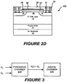
- the steam used in the wet O 2 anneal process may be generated using a pyrogenic process, and the resulting wet O 2 anneal may be referred to as a "pyrogenic oxidation.”
- a pyrogenic oxidation oxygen (O 2 ) gas and hydrogen (H 2 ) gas are flowed into a pyrogenic chamber 210, which is separate from the anneal chamber 220, and which is heated to a high temperature, such as about 800 °C.
- the hydrogen and oxygen gas combust in the pyrogenic chamber 210 and form a mixture of steam (H 2 O) and oxygen (O 2 ), which is supplied to the anneal chamber 220.
- a polysilicon gate 28 may be deposited and doped, for example, with boron followed by a metallization process to reduce the gate resistance.
- An interlayer dielectric layer 33 for example of silicon dioxide, is formed on the structure 10D and covers the gate 28 and exposed portions of the structure 10D. Via holes are opened in the interlayer dielectric layer 33, and ohmic contacts are formed to the p-type emitter regions 22 and the n-type connector regions 24.
- An Al-based conductive material such as Al and/or AlSi, may be deposited as the p-type ohmic metal emitter contacts 37, and aNi-based conductive layer such as Ni and/or Ni/Si may be deposited as the n-type ohmic metal contacts 35. All contacts may be sintered in Rapid Thermal Annealer.
- a metal overlayer 39 such as a thick Ti/Au layer, may be deposited on the interlayer dielectric layer to electrically connect the p-type emitter regions 22 and the n-type connector regions 24.
- An n-type collector contact 32 is formed as a backside contact on the device 10.
- a planar IGBT as described above and having an active area of 0.4 mm 2 was fabricated and characterized for on-state and blocking characteristics with negative potentials on the gate and collector.
- the on-state characteristics at room temperature of a 0.4 mm 2 IGBT are shown in Fig. 4 with a maximum gate bias of about -20 V.
- the knee voltage is about -3 V, which indicates good ohmic contacts on the emitter and collector.
- the differential on-resistance is 88 m ⁇ cm 2 which is the lowest value for high voltage IGBTs. Setting the power dissipation for such devices at 300 W/cm 2 , the collector current density is approximately 50 A/cm 2 . At this current density level, the collector voltage drop is about -8.65 V, which corresponds to a specific on-resistance of about 173 m ⁇ cm 2 .
- an IGBT may exhibit a positive temperature coefficient.
- Fig. 5 shows the I-V characteristics at 200°C for the same device.
- the knee voltage stays relatively constant at -3 V.
- the differential on-resistance further reduces to about 25 m ⁇ cm 2 at a gate bias of -20 V.
- the collector voltage drop reduces to about -5.30 V, which corresponds to a specific on-resistance of about 106 m ⁇ cm 2 .
- the on-resistance reduction at high temperature may indicate that carrier lifetimes in SiC materials currently used are the dominant factor relating to IGBT on-state current conduction capability.
- an IGBT according to some embodiments of the invention still exhibits a higher voltage drop at room temperature, possibly due to insufficient resistivity modulation. However, the voltage drop becomes less than the value for the DMOSFET at high temperatures.
- Fig. 6 shows the voltage blocking characteristics of the same device at room temperature.
- an IGBT device as described above was tested with the gate electrode grounded with the emitter and immersed in Fluorinert to prevent arcing in air.
- a 9 kV blocking voltage with a leakage current density of less than about 0.1 mA/cm 2 has been achieved at gate bias of 0 V.
- the breakdown occurs in the device termination periphery, which may indicate that there is room to approach the blocking voltage determined by the drift layer thickness with a better edge termination design.
- IGBT devices were used for the switching tests.
- a clamped Inductive Switching Test Circuit topology as shown in Fig. 7 was used for the switching tests.
- the IGBT device 10 tested in the switching tests had an active area of 4 mm 2 to achieve a high conduction current, but otherwise the test device had a similar design as that described above.
- the IGBT 10 is coupled to a 1.1 mH inductive load L1 that is clamped by a freewheeling diode D1.
- the diode D1 includes two Cree CSD10120 SiC Schottky diodes in series with zero reverse recovery. One CSD10120 diode is rated for 1200 V and 10 A, so two in series may provide 2400 V of blocking capability.
- the capacitor C1 has a capacitance of 2 ⁇ F and is capable of handling voltages up to 4 kV.
- a negative pulse from 0 to - 20 V from the voltage source Vin was used to turn-on the IGBT.
- the supply voltage Vss is -500 V.
- Fig. 8 shows the switching waveforms at 25°C with a collector voltage of - 500 V.
- the horizontal axis measures time at 500 nsec/div, while the vertical axis measures volts at 200 V/div and current at 1 A/div.
- the fall time tfall is defined as the time to take the collector current to fall from 90% to 5% of its 2 A peak at turn-off.
- the rise time trise is the time it takes for the collector current to rise from 5% to 90% of the 2 A current peak at turn-on.
- the turn-on delay time is the time between the -20 gate bias being applied and the collector current rising to the 2 A peak.
- the turn-off delay time is the time between the removal of the gate bias and fall of the collector current towards zero.
- Table 1 shows the switching times for varying temperatures.
- the total switching time is about 350 ns at room temperature and increases to about 460 ns at 200°C.
- the IGBT features a fast switching capability, which can be operated at high frequency for a wide temperature range.
- the turn-off delay time may be the dominant portion of the total switching time, which is primarily determined by the input capacitors.
- SiC IGBTs may be suitable for high power and/or high temperature applications. Some embodiments of the invention provide high voltage planar IGBTs on n-type 4H-SiC substrates. In some embodiments, a differential on-resistance of about 88 m ⁇ cm 2 at a gate bias of about -20 V is achieved at 25°C, and decreases to about 24.8 m ⁇ cm 2 at 200°C. A device according to embodiments of the invention may exhibit a blocking voltage of about 9 kV with a leakage current density of about 0.1 mA/cm 2 or less.
- IGBTs according to some embodiments of the invention may exhibit fast switching capability at both room temperature and at elevated temperatures.
- IGBT devices may exhibit a low on-state resistance.
- a high channel mobility may be achieved by using one or more of buried channel implantation/regrowth, thermal oxidation, high temperature implant activation and/or graphite encapsulation during implant activation.
- Some embodiments of the invention may provide an optimized cell design with a better trade-off between high channel density and low JFET resistance.
- some embodiments of the invention may provide a field stopper layer that is configured to enhance the carrier injection efficiency while maintaining a desired blocking capability.
- High channel mobility may be obtained through epitaxial channel regrowth and/or activation of threshold adjustment/buried channel implants using a high temperature anneal and/or graphite encapsulation.
- High majority carrier injection from the P-type emitter may be obtained through P-type epitaxial growth to obtain a high hole carrier concentration.
- some embodiments of the invention may provide reduced ohmic contact resistance on n- and p-type materials.
Description
- The present invention relates to electronic devices. More particularly, the present invention relates to high power insulated gate bipolar transistors.
- Power devices made with silicon carbide (SiC) are expected to show great advantages as compared to those on silicon for high speed, high power and/or high temperature applications due to the high critical field and wide band gap of SiC. For devices capable of blocking high voltages, such as voltages in excess of about 5 kV, it may be desirable to have bipolar operation to reduce the drift layer resistance via conductivity modulation resulting from injected minority carriers. However, one technical challenge for bipolar devices in silicon carbide is forward voltage degradation over time, possibly due to the presence of Basal Plane Dislocations (BPD) in single crystals of silicon carbide. Thus, unipolar devices such as SiC Schottky diodes and MOSFETs are typically used for high power applications.
- SiC DMOSFET devices with a 10 kV blocking capability have been fabricated with a specific on-resistance of about 100 mΩ×cm2. DMOSFET devices may exhibit very fast switching speed of, for example, less than 100 ns, due to their majority carrier nature. However, as the desired blocking voltage of devices increases, for example up to 15 kV or more, the on-resistance of a MOSFET device may increase substantially, due to the corresponding increase in the drift layer thickness. This problem may be exacerbated at high temperatures due to bulk mobility reduction, which may result in excessive power dissipation.
- With the progress of SiC crystal material growth, several approaches have been developed to mitigate BPD related problems. See, e.g., B. Hull, M. Das, J. Sumakeris, J. Richmond, and S. Krishinaswami, "Drift-Free 10-kV, 20-A 4H-SiC PiN Diodes", Journal of Electrical Materials, Vol. 34, No. 4, 2005. These developments may enhance the development and/or potential applications of SiC bipolar devices such as thyristors, GTOs, etc. Even though thyristors and/or GTOs may offer low forward voltage drops, they may require bulky commutating circuits for the gate drive and protections. Accordingly, it may be desirable for a SiC bipolar device to have gate turn-off capability. Due to their superior on-state characteristics, reasonable switching speed, and/or excellent safe-operation-area (SOA), 4H-SiC insulated gate bipolar transistors (IGBTs) are becoming more suitable for power switching applications.
US 2005/0012143 A1 relates to a semiconductor device and method of manufacturing the same. - The present invention provides an insulated gate bipolar transistor (IGBT) according to
claim 1. - The silicon carbide drift layer may include a JFET region adjacent to the well region. The emitter region may be spaced apart from the JFET region and may define the channel region between the emitter region and the JFET region.
- The first conductivity type is n-type and the second conductivity type is p-type.
- The transistor may further include a connector region of the first conductivity type extending from a surface of the channel adjustment layer into the well region, a first ohmic contact on the connector region, a second ohmic contact on the emitter region and including a material different from the first ohmic contact, and a metal overlayer electrically connecting the first ohmic contact and the second ohmic contact.
- The first ohmic contact may include a nickel-based conductive material and the second ohmic contact may include an aluminum-based conductive material.
- The channel adjustment layer may have a thickness of about 0.25 µm or more. Furthermore, the distance from a bottom of the emitter region to a bottom of the well region is 0.45 µm or more.
The channel adjustment layer may have a thickness of about 0.1 µm to about 0.5 µm, and a net doping concentration of about 1 x 1016 cm-3 to about 5 x 1018 cm-3. - The invention provides a method of forming an insulated gate bipolar transistor (IGBT) device in silicon carbide according to claim 5.
- The method further includes forming a graphite coating for implant activation and removing the graphite coating after annealing the implanted ions. Annealing the implanted ions includes annealing the silicon carbide layer and the graphite coating. The methods may further include crystallizing the graphite coating before annealing the implanted ions.
- Annealing the implanted ions may include annealing the implanted ions at a temperature greater than 1700 °C, and in some embodiments greater than 1800 °C. Forming the gate oxide layer may include forming the gate oxide layer in dry O2, the method may further include annealing the gate oxide layer in wet O2. In particular, forming the gate oxide layer may include forming the gate oxide layer in dry O2 at a temperature less than or equal to about 1200 °C.
- The methods may further include annealing the gate oxide layer in an inert atmosphere at a temperature less than or equal to about 1200 °C after forming the gate oxide layer and before annealing the gate oxide layer in wet O2.
- Annealing the gate oxide layer in wet O2 may include annealing the gate oxide layer in wet O2 at a temperature less than or equal to about 950 °C for at least one hour.
- Annealing the oxide layer in wet O2 may include generating pyrogenic steam in a pyrogenic chamber, supplying the pyrogenic steam to an anneal chamber, and annealing the oxide layer in the anneal chamber. Generating pyrogenic steam may include heating the pyrogenic chamber, supplying hydrogen and oxygen gas to the pyrogenic chamber, and combusting the hydrogen gas and the oxygen gas to form the pyrogenic steam, the hydrogen gas and the oxygen gas are supplied to the pyrogenic chamber at a molecular ratio of hydrogen to oxygen of about 1.8 or more.
- The methods may further include implanting p-type dopant ions into the drift layer to form a JFET region adjacent to the n-type well. The p-type emitter region may be spaced apart from the JFET region and may define a channel region between the p-type emitter region and the JFET region.
- The channel adjustment layer may have a thickness of about 0.1 µm to about 0.5 µm, and a net acceptor concentration of about 1 x 1016 cm-3 to about 5 x 1018 cm-3.
- The accompanying drawings, which are included to provide a further understanding of the invention and are incorporated in and constitute a part of this application, illustrate certain embodiment(s) of the invention. In the drawings:
-
Figure 1 is a cross-section of a silicon carbide insulated gate bipolar transistor (IGBT) device according to some embodiments of the invention. -
Figures 2A to 2D are cross-section illustrations showing intermediate structures in the formation of an IGBT device according to some embodiments of the invention. -
Figure 3 is a schematic diagram illustrating a pyrogenic chamber and an anneal chamber that may be used according to some embodiments of the invention. -
Figures 4-5 are plots of on-state I-V characteristics for an IGBT device according to some embodiments of the invention. -
Figure 6 is a graph of leakage current density versus blocking voltage for an IGBT device according to some embodiments of the invention. -
Figure 7 is a diagram of a clamped inductive switching test circuit topology used for testing the switching characteristics of a device according to some embodiments of the invention. -
Figure 8 is a graph of an inductive switching waveform of a device according to some embodiments of the invention. - Embodiments of the present invention now will be described more fully hereinafter with reference to the accompanying drawings, in which embodiments of the invention are shown. This invention may, however, be embodied in many different forms and should not be construed as limited to the embodiments set forth herein. Rather, these embodiments are provided so that this disclosure will be thorough and complete, and will fully convey the scope of the invention to those skilled in the art. Like numbers refer to like elements throughout.
- It will be understood that, although the terms first, second, etc. may be used herein to describe various elements, these elements should not be limited by these terms. These terms are only used to distinguish one element from another. For example, a first element could be termed a second element, and, similarly, a second element could be termed a first element, without departing from the scope of the present invention. As used herein, the term "and/or" includes any and all combinations of one or more of the associated listed items.
- The terminology used herein is for the purpose of describing particular embodiments only and is not intended to be limiting of the invention. As used herein, the singular forms "a", "an" and "the" are intended to include the plural forms as well, unless the context clearly indicates otherwise. It will be further understood that the terms "comprises" "comprising," "includes" and/or "including" when used herein, specify the presence of stated features, integers, steps, operations, elements, and/or components, but do not preclude the presence or addition of one or more other features, integers, steps, operations, elements, components, and/or groups thereof.
- Unless otherwise defined, all terms (including technical and scientific terms) used herein have the same meaning as commonly understood by one of ordinary skill in the art to which this invention belongs. It will be further understood that terms used herein should be interpreted as having a meaning that is consistent with their meaning in the context of this specification and the relevant art and will not be interpreted in an idealized or overly formal sense unless expressly so defined herein.
- It will be understood that when an element such as a layer, region or substrate is referred to as being "on" or extending "onto" another element, it can be directly on or extend directly onto the other element or intervening elements may also be present. In contrast, when an element is referred to as being "directly on" or extending "directly onto" another element, there are no intervening elements present. It will also be understood that when an element is referred to as being "connected" or "coupled" to another element, it can be directly connected or coupled to the other element or intervening elements may be present. In contrast, when an element is referred to as being "directly connected" or "directly coupled" to another element, there are no intervening elements present.
- Relative terms such as "below" or "above" or "upper" or "lower" or "horizontal" or "lateral" or "vertical" may be used herein to describe a relationship of one element, layer or region to another element, layer or region as illustrated in the figures. It will be understood that these terms are intended to encompass different orientations of the device in addition to the orientation depicted in the figures.
- Embodiments of the invention are described herein with reference to cross-section illustrations that are schematic illustrations of idealized embodiments (and intermediate structures) of the invention. The thickness of layers and regions in the drawings may be exaggerated for clarity. Additionally, variations from the shapes of the illustrations as a result, for example, of manufacturing techniques and/or tolerances, are to be expected. Thus, embodiments of the invention should not be construed as limited to the particular shapes of regions illustrated herein but are to include deviations in shapes that result, for example, from manufacturing. For example, an implanted region illustrated as a rectangle will, typically, have rounded or curved features and/or a gradient of implant concentration at its edges rather than a discrete change from implanted to non-implanted region. Likewise, a buried region formed by implantation may result in some implantation in the region between the buried region and the surface through which the implantation takes place. Thus, the regions illustrated in the figures are schematic in nature and their shapes are not intended to illustrate the actual shape of a region of a device and are not intended to limit the scope of the invention.
- Some embodiments of the invention are described with reference to semiconductor layers and/or regions which are characterized as having a conductivity type such as n-type or p-type, which refers to the majority carrier concentration in the layer and/or region. Thus, n-type material has a majority equilibrium concentration of negatively charged electrons, while p-type material has a majority equilibrium concentration of positively charged holes. Some material may be designated with a "+" or "-" (as in n+, n-, p+, p-, n++, n--, p++, p--, or the like), to indicate a relatively larger ("+") or smaller ("-") concentration of majority carriers compared to another layer or region. However, such notation does not imply the existence of a particular concentration of majority or minority carriers in a layer or region.
- Some embodiments of the invention provide insulated gate bipolar transistors (IGBTs) that are suitable for high power and/or high temperature applications. Some embodiments of the invention provide high voltage planar IGBTs. Although embodiments of the invention described herein include silicon carbide substrates and epitaxial layers, the principles and structures described herein may be advantageously employed in devices formed using other materials, such as silicon, germanium, gallium arsenide, and gallium nitride, and alloys thereof.
- The first reported planar gate 5.8 kV IGBT in SiC was built on an n-type substrate in 2005. See, Q. Zhang, C. Jonas, S.Ryu, A. Agarwal and J. Palmour "Design and Fabrications of High Voltage IGBTs on 4H-SiC", ISPSD Proceeding, 2006. The p-channel IGBT was selected due to the lack of high quality, low resistivity p-SiC substrates, which are required for n-channel IGBTs. The device exhibits a differential on-resistance (Rdiff, on) of about 570 mΩ×cm2 at a gate bias of -30 V at 25°C, and decreases to about 118 mΩ×cm2 at 200°C, respectively. The high on-resistance was primarily attributed to the low bulk carrier lifetimes, and low hole channel mobility.
- An IGBT structure according to some embodiments of the invention is shown in
Fig. 1 . A planar device structure, such as the structure of thedevice 10 shown inFig. 1 , may provide process simplification and/or enhanced device reliability. However, other device structures may be advantageously employed. - The
device 10 ofFig. 1 includes a p-type buffer layer 14 and a p-drift epitaxial layer 16 on an n-type substrate 12. Thesubstrate 12 may include an n+-type, 8° off-axis 4H-SiC substrate. The p-drift layer 16 may have a thickness of about 110 µm and may be doped with p-type dopants at a doping concentration selected to provide a desired blocking voltage. For example, the p-drift layer 16 may be doped with p-type dopants at a doping concentration of about 2 x 1014 cm-3 to about 6 x 1014 cm-3 for a 10 kV blocking capability. The p-type buffer layer 14 may have a thickness of about 1 µm to about 2 µm and may be doped with p-type dopants at a doping concentration of about 1x1017 cm-3. The p-type buffer layer 14 is provided as a channel stop layer to discourage punch-through. - N+ well
regions 18 are formed at a surface of the p-type drift layer 16. The n+ wellregions 18, which may be formed by ion implantation, may extend a distance of about 0.5 µm into thedrift layer 16. - An epitaxial p-type
channel adjustment layer 40 is on thedrift layer 16. Thechannel adjustment layer 40 may have a thickness of about 0.1 µm to about 0.5 µm, and may be doped with p-type dopants to have a net acceptor concentration of about 1 x 1016 cm-3 to about 5 x 1018 cm-3. In particular, the epitaxial p-typechannel adjustment layer 40 may have a thickness of about 0.25 µm and may be doped with acceptor ions, such as aluminum ions, at a doping concentration of about 1 x 1017 cm-3. The presence of the p-typechannel adjustment layer 40 may modify the threshold voltage and/or improve the inversion channel mobility of thedevice 10. - The
device 10 further includesn+ connector regions 24 andp+ emitter regions 22 that may be formed by selective implantation of, for example, nitrogen and aluminum, respectively. Then+ connector regions 24 andp+ emitter regions 22 extend through the p-typechannel adjustment layer 40 and into the n+ wellregions 18. In some embodiments, a distance d between the bottom of thep+ emitter regions 22 and the bottom of the n+ wellregions 18 may be about 0.45 µm or more. An increased distance d may provide a lower resistance of the n+ wellregions 18, which may result in improved on-state resistance of thedevice 10. - A guard-ring based edge termination (not shown) may be provided around the device periphery. Other types of edge terminations may be used.
- The
device 10 includes aJFET region 20 in thedrift layer 16 between adjacent n+ wellregions 18. TheJFET region 20 may be implanted with p-type dopants to reduce the JFET resistance from the adjacent n+ wellregions 18. In some embodiments, theJFET region 20 may be formed by an epitaxial growth process. - The
device 10 further includes agate insulation layer 26, which may include silicon dioxide having a thickness of about 400-1000Å. - A
gate 28 of, for example, polysilicon is formed on thegate insulation layer 26. Aninterlayer dielectric layer 33 is on the surface of thedevice 10 and electrically insulates thegate 28. - N-
type ohmic contacts 35 are formed to then+ connector regions 24, and p-type ohmic contacts 37 are formed to thep+ emitter regions 22. The n-type ohmic contacts 35 may include a nickel-based conductive layer, such as Ni and/or NiSi. The p-type ohmic contact 37 may include an aluminum-based conductive layer, such as Al and/or AlSi. A metal overlayer 39 is formed on theinterlayer dielectric layer 33 and electrically connects the n-type connector regions 24 and the p-type emitter regions 22 through their respectiveohmic contacts metal collector contact 32 is formed on thesubstrate 12. -
Figures 2A to 2D illustrate some operations that may be performed andintermediate structures 10A to 10D that may be formed during the formation of adevice 10. Referring toFigure 2A , a p-type SiC buffer 14 and a p-SiC drift layer 16 are formed by epitaxial growth on an n+-type 8° off-axis 4H-SiC substrate 12. The p-type buffer layer 14 may have a thickness of about 1 µm to about 2 µm and may be doped with p-type dopants at a doping concentration of about 1x1017 cm-3. After formation of the p-type drift layer 16, the n+ wellregions 18 are formed, for example, by implantation of donor ions, such as nitrogen, into thedrift layer 16. It may be desirable to implant the n+well regions 18 as deep as possible. The depth of the n+ wellregions 18 may be limited by the available implant energy. - The structure may then be annealed at a temperature of about 1600 °C or more to activate the implanted ions. In particular, the structure may be annealed under standard SiC activation annealing conditions that are known in the art to activate the n-type dopants.
- The
JFET region 20 may be formed, for example, by implantation of aluminum in thedrift layer 16 between adjacent n+ wellregions 18. TheJFET region 20 may be implanted with p-type dopants to reduce the JFET resistance from the adjacent n+ wellregions 18. In particular, the JFET implantation dose may be selected to reduce the JFET resistance while keeping implant damage at an acceptable level. In some embodiments, the JFET implantation may be performed at a dose sufficient to provide a dopant concentration of about 1x1016 cm-3 in theJFET region 20. The JFET region may, in some embodiments, be formed by an epitaxial growth process. - Referring to
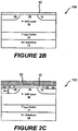
Figure 2B , an epitaxialchannel adjustment layer 40 is formed on thedrift layer 16, for example using well-known SiC epitaxial regrowth techniques. Thechannel adjustment layer 40 may be doped with acceptor ions at a doping concentration of about 1 x 1017 cm-3. - The epitaxial
channel adjustment layer 40 may modify the threshold voltage and/or improve the inversion channel mobility of the device. Furthermore, thechannel adjustment layer 40 may also permit formation of shallower p-type source regions 22 relative to the n-type well regions 18. Providing deeper n-type well regions 18 by lifting the p-type emitter implants 22 to the surface of the regrownchannel adjustment layer 40 may reduce or prevent latch-up in the device. The deep n+ well 18 may result in a lower N-well resistance due to the increased spacing d between the bottom of the p-type emitter region 22 and the bottom of the n+ well 18. A lower n-well resistance may increase the device latch-up current and/or provide a better on-state resistance. - Referring to
Figure 2C , the n-type connector regions 24 and p-type emitter regions 22 are formed, for example, by selective implantation of donor and acceptor ions, respectively, into/through the epitaxialchannel adjustment layer 40. - It will be appreciated that the distance d shown in
Figure 2C is a function of the vertical extent of the n-type well regions 18 and the vertical extent of the p-type emitter regions 22. In general, it may be desirable to make the spacing d between the bottom of the p-type emitter regions 22 and the bottom of the n+ well 18 regions as large as possible. Furthermore, as described above, the p-type emitter regions 22 may be formed after formation of the p-type epitaxialchannel adjustment layer 40. Thus, the thickness (depth) of thewell regions 18 is determined by the maximum implant energy of the system used to manufacture the device. However, the penetration depth of thep+ emitter regions 22 into the n-type well regions 18 may be decreased by the thickness of the epitaxialchannel adjustment layer 40, which may be about 0.25 µm. - Still referring to
Figure 2C , the implanted dopants may be activated by annealing the structure at a temperature of about 1600°C or more with a silicon over pressure and/or covered by an encapsulation layer such as a graphite film. In some embodiments, the implants may be activated by annealing at a temperature greater than about 1700 °C using a graphite encapsulation layer. - A high temperature activation anneal (e.g. 1700 °C or more) may enhance the activation of the threshold adjustment ions, as well as annealing of defects in the
channel region 40. However, such a high temperature anneal may damage the surface of the siliconcarbide drift layer 16. - Referring to
Fig. 2C , in order to reduce damage that may result from a high temperature anneal, agraphite coating 50 may be formed on the surface of thestructure 10C prior to formation of thegate oxide 26,gate contact 28 and emitter contact 30. That is, prior to annealing thestructure 10C to activate the implanted ions, agraphite coating 50 may be applied to the top/front side of thestructure 10C in order to protect the surface of the structure during the anneal. Thegraphite coating 50 may be applied by a conventional resist coating method and may have a thickness that is sufficient to protect the underlying SiC layers during a high temperature anneal. For example, thegraphite coating 50 may have a thickness of about 1 µm. Thegraphite coating 50 may be heated to form a crystalline coating on thechannel adjustment layer 40. The implanted ions may be activated by a thermal anneal that may be performed, for example, in an inert gas at a temperature of about 1700 °C or greater. In particular the thermal anneal may be performed at a temperature of about 1850 °C in argon for 5 minutes. Thegraphite coating 50 may help to protect the surface of the epitaxialchannel adjustment layer 40 and/or thedrift layer 16 during the high temperature anneal. - The
graphite coating 50 may then be removed, for example, by ashing and thermal oxidation. - After implant annealing, a field oxide (not shown) of, for example, silicon dioxide having a thickness of about 1 µm may be deposited and patterned to expose the active region of the device.
- Referring to
Fig. 2D , thegate insulation layer 26 may be formed by a gate oxidation process, with a final gate oxide thickness of 400-600Å. - The
gate insulation layer 26 may be grown on the exposed surface of thedrift layer 16 after removal of thegraphite cap layer 50. Thegate insulation layer 26 may include an oxide layer grown by a dry-wet oxidation process that includes a growth of bulk oxide in dry O2 followed by an anneal of the bulk oxide in wet O2 as described, for example, inU.S. Patent No. 5,972,801 ,. As used herein, anneal of oxide in wet O2 refers to anneal of an oxide in an ambient containing both O2 and vaporized H2O. An anneal may be performed in between the dry oxide growth and the wet oxide growth. The dry O2 oxide growth may be performed, for example, in a quartz furnace tube at a temperature of up to about 1200 °C in dry O2 for a time of at least about 2.5 hours. Dry oxide growth is performed to grow the bulk oxide layer to a desired thickness. The temperature of the dry oxide growth may affect the oxide growth rate. For example, higher process temperatures may produce higher oxide growth rates. The maximum growth temperature may be dependent on the system used. Higher temperatures may be achieved for the dry O2 growth by using, for example, a silicon carbide furnace instead of a quartz tube. However, higher temperatures may not improve the quality of the oxide. - In some embodiments, the dry O2 oxide growth may be performed at a temperature of about 1175 °C in dry O2 for about 3.5 hours. The resulting oxide layer may be annealed at a temperature of up to about 1200 °C in an inert atmosphere. In particular, the resulting oxide layer may be annealed at a temperature of about 1175 °C in Ar for about 1 hour.
- The wet O2 oxide anneal may be performed at a temperature of about 950 °C or less for a time of at least about 1 hour. The temperature of the wet O2 anneal may be limited to discourage further thermal oxide growth at the SiC/SiO2 interface, which may introduce additional interface states. In particular, the wet O2 anneal may be performed in wet O2 at a temperature of about 950 °C for about 3 hours. The resulting
gate insulation layer 26 may have a thickness of about 500 A. - In some embodiments, the steam used in the wet O2 anneal process may be generated using a pyrogenic process, and the resulting wet O2 anneal may be referred to as a "pyrogenic oxidation." Referring to
Figure 3 , in a pyrogenic oxidation, oxygen (O2) gas and hydrogen (H2) gas are flowed into apyrogenic chamber 210, which is separate from theanneal chamber 220, and which is heated to a high temperature, such as about 800 °C. The hydrogen and oxygen gas combust in thepyrogenic chamber 210 and form a mixture of steam (H2O) and oxygen (O2), which is supplied to theanneal chamber 220. - In some cases, it may be desirable to adjust the flow rates of hydrogen and oxygen into the
pyrogenic chamber 210 so that a molecular ratio of hydrogen to oxygen approaches, but does not exceed, a 2:1 ratio. That is, it may be desirable for the mixture supplied to theanneal chamber 220 to be as wet as possible, within reasonable safety limits. In some cases, a hydrogen/oxygen ratio of 1.8:1 or 1.9:1 may be used. - Referring again to
Figure 2D , after formation of thegate insulation layer 26, apolysilicon gate 28 may be deposited and doped, for example, with boron followed by a metallization process to reduce the gate resistance. Aninterlayer dielectric layer 33, for example of silicon dioxide, is formed on thestructure 10D and covers thegate 28 and exposed portions of thestructure 10D. Via holes are opened in theinterlayer dielectric layer 33, and ohmic contacts are formed to the p-type emitter regions 22 and the n-type connector regions 24. An Al-based conductive material, such as Al and/or AlSi, may be deposited as the p-type ohmicmetal emitter contacts 37, and aNi-based conductive layer such as Ni and/or Ni/Si may be deposited as the n-typeohmic metal contacts 35. All contacts may be sintered in Rapid Thermal Annealer. As shown inFigure 1 , a metal overlayer 39, such as a thick Ti/Au layer, may be deposited on the interlayer dielectric layer to electrically connect the p-type emitter regions 22 and the n-type connector regions 24. An n-type collector contact 32 is formed as a backside contact on thedevice 10. - A planar IGBT as described above and having an active area of 0.4 mm2 was fabricated and characterized for on-state and blocking characteristics with negative potentials on the gate and collector. The on-state characteristics at room temperature of a 0.4 mm2 IGBT are shown in
Fig. 4 with a maximum gate bias of about -20 V. The knee voltage is about -3 V, which indicates good ohmic contacts on the emitter and collector. The differential on-resistance is 88 mΩ×cm2 which is the lowest value for high voltage IGBTs. Setting the power dissipation for such devices at 300 W/cm2, the collector current density is approximately 50 A/cm2. At this current density level, the collector voltage drop is about -8.65 V, which corresponds to a specific on-resistance of about 173 mΩ×cm2. - In the on-state, an IGBT according to embodiments of the invention may exhibit a positive temperature coefficient.
Fig. 5 shows the I-V characteristics at 200°C for the same device. The knee voltage stays relatively constant at -3 V. The differential on-resistance further reduces to about 25 mΩ×cm2 at a gate bias of -20 V. At the collector current density of 50 A/cm2, the collector voltage drop reduces to about -5.30 V, which corresponds to a specific on-resistance of about 106 mΩ×cm2. The on-resistance reduction at high temperature may indicate that carrier lifetimes in SiC materials currently used are the dominant factor relating to IGBT on-state current conduction capability. Compared to a 10 kV-class SiC DMOSFET, an IGBT according to some embodiments of the invention still exhibits a higher voltage drop at room temperature, possibly due to insufficient resistivity modulation. However, the voltage drop becomes less than the value for the DMOSFET at high temperatures. -
Fig. 6 shows the voltage blocking characteristics of the same device at room temperature. In particular, an IGBT device as described above was tested with the gate electrode grounded with the emitter and immersed in Fluorinert to prevent arcing in air. As shown inFig. 6 , a 9 kV blocking voltage with a leakage current density of less than about 0.1 mA/cm2 has been achieved at gate bias of 0 V. The breakdown occurs in the device termination periphery, which may indicate that there is room to approach the blocking voltage determined by the drift layer thickness with a better edge termination design. - Hole mobility and MOS threshold voltage measurements for a lateral 4H-SiC p-MOSFET fabricated in conjunction with the IGBT show that the MOSFET device has a peak channel mobility of about 6.5 cm2/V-s and a threshold voltage of about -7.5 V at room temperature. The channel mobility reaches a maximum value of about 8.2 cm2/V-s at 100°C, while the threshold voltage decreases with temperature.
- Switching tests were performed on IGBT devices according to embodiments of the invention. A clamped Inductive Switching Test Circuit topology as shown in
Fig. 7 was used for the switching tests. TheIGBT device 10 tested in the switching tests had an active area of 4 mm2 to achieve a high conduction current, but otherwise the test device had a similar design as that described above. In this test circuit, theIGBT 10 is coupled to a 1.1 mH inductive load L1 that is clamped by a freewheeling diode D1. The diode D1 includes two Cree CSD10120 SiC Schottky diodes in series with zero reverse recovery. One CSD10120 diode is rated for 1200 V and 10 A, so two in series may provide 2400 V of blocking capability. The capacitor C1 has a capacitance of 2 µF and is capable of handling voltages up to 4 kV. A negative pulse from 0 to - 20 V from the voltage source Vin was used to turn-on the IGBT. The supply voltage Vss is -500 V. -
Fig. 8 shows the switching waveforms at 25°C with a collector voltage of - 500 V. InFig. 8 ; the horizontal axis measures time at 500 nsec/div, while the vertical axis measures volts at 200 V/div and current at 1 A/div. The fall time tfall is defined as the time to take the collector current to fall from 90% to 5% of its 2 A peak at turn-off. The rise time trise is the time it takes for the collector current to rise from 5% to 90% of the 2 A current peak at turn-on. The turn-on delay time is the time between the -20 gate bias being applied and the collector current rising to the 2 A peak. The turn-off delay time is the time between the removal of the gate bias and fall of the collector current towards zero. - Table 1 shows the switching times for varying temperatures. The total switching time is about 350 ns at room temperature and increases to about 460 ns at 200°C. The IGBT features a fast switching capability, which can be operated at high frequency for a wide temperature range. The turn-off delay time may be the dominant portion of the total switching time, which is primarily determined by the input capacitors.
Table 1 - Switching Times Temp. (C) tfull (ns) trise (ns) tdelay(on) (ns) tdelay(off) (ns) ttotal (ns) 25 64 14 40 220 338 50 81 16 20 220 337 100 51 10 18 220 299 150 75 14 18 320 427 200 77 7 36 340 460 - SiC IGBTs according to some embodiments of the invention may be suitable for high power and/or high temperature applications. Some embodiments of the invention provide high voltage planar IGBTs on n-type 4H-SiC substrates. In some embodiments, a differential on-resistance of about 88 mΩ×cm2 at a gate bias of about -20 V is achieved at 25°C, and decreases to about 24.8 mΩ×cm2 at 200°C. A device according to embodiments of the invention may exhibit a blocking voltage of about 9 kV with a leakage current density of about 0.1 mA/cm2 or less. A hole channel mobility of about 6.5 cm2/V-s is achieved at room temperature with a threshold voltage of -6.5 V, resulting in enhanced conduction capability. Inductive switching tests show that IGBTs according to some embodiments of the invention may exhibit fast switching capability at both room temperature and at elevated temperatures.
- IGBT devices according to some embodiments of the invention may exhibit a low on-state resistance. In particular, a high channel mobility may be achieved by using one or more of buried channel implantation/regrowth, thermal oxidation, high temperature implant activation and/or graphite encapsulation during implant activation. Some embodiments of the invention may provide an optimized cell design with a better trade-off between high channel density and low JFET resistance. Furthermore, some embodiments of the invention may provide a field stopper layer that is configured to enhance the carrier injection efficiency while maintaining a desired blocking capability. High channel mobility may be obtained through epitaxial channel regrowth and/or activation of threshold adjustment/buried channel implants using a high temperature anneal and/or graphite encapsulation. High majority carrier injection from the P-type emitter may be obtained through P-type epitaxial growth to obtain a high hole carrier concentration. Furthermore, some embodiments of the invention may provide reduced ohmic contact resistance on n- and p-type materials.
- In the drawings and specification, there have been disclosed typical embodiments of the invention and, although specific terms are employed, they are used in a generic and descriptive sense only and not for purposes of limitation, the scope of the invention being set forth in the following claims.
Claims (6)
- An insulated gate bipolar transistor (10), comprising:a substrate (12) having a first conductivity type;a drift layer (16) having a second conductivity type opposite the first conductivity type;a well region (18) in the drift layer (16) and having the first conductivity type;an epitaxial channel adjustment layer (40) on the drift layer (16) and having the second conductivity type and having a thickness of about 0.25 µm or more;an emitter region (22) extending from a surface of the epitaxial channel adjustment layer (40) through the epitaxial channel adjustment layer (40) and into the well region (18), the emitter region (22) having the second conductivity type and at least partially defining a channel region in the well region (18) adjacent to the emitter region (22);a gate oxide layer on the channel region; anda gate on the gate oxide layer wherein the first conductivity type is n-type and the second conductivity type is p-type,characterised in that a distance from a bottom of the emitter region (22) to a bottom of the well region (18) is 0.45 µm or more.
- The transistor (10) of Claim 1, wherein the channel adjustment layer (40) has a thickness of about 0.25 µm to about 0.5 µm and a net doping concentration of about 1 x 1016 cm-3 to about 5 x 1018 cm-3.
- The transistor (10) of Claim 1, wherein the substrate (12) comprises a silicon carbide substrate (12) and wherein the drift layer (16) comprises a silicon carbide epitaxial layer on the substrate (12).
- The transistor (10) of Claim 1, wherein the transistor (10) further comprises:an n-type connector region (24) extending through the channel adjustment layer (40) and into the n-type well region (18);a first ohmic contact (37) including aluminum on the p-type emitter region (22);a second ohmic contact (35) including a metal different from the first ohmic contact (37) on the n-type connector region (24), the second ohmic contact (35) comprising nickel;an interlayer dielectric layer (33) on the gate, the interlayer dielectric layer (33) including a first opening exposing the first ohmic contact (37) and a second opening exposing the second ohmic contact (35); anda metal overlayer (39) on the interlayer dielectric layer (33) and electrically connecting the first ohmic contact (37) and the second ohmic contact (35).
- A method of forming an insulated gate bipolar transistor (IGBT) device (10), comprising:forming a p-type drift layer (16) on an n-type substrate (12);forming an n-type well in the p-type drift layer (16);epitaxially growing a p-type channel adjustment layer (40) on the p-type drift layer (16) and on the n-type well;implanting p-type dopant ions to form a p-type emitter region (22) extending through the channel adjustment layer (40) and into the n-type well at a surface of the drift layer (16), the p-type emitter region (22) at least partially defining a channel region in the n-type well adjacent the p-type emitter region (22);implanting n-type dopant ions to form an n-type connector region (24) extending through the channel layer and into the n-type well at a surface of the drift layer (16);forming a graphite coating (50) on the channel adjustment layer (40);annealing the implanted ions and the graphite coating (50);removing the graphite coating (50) after annealing the implanted ions;forming a gate oxide layer on the channel region; andforming a gate on the gate oxide layer,wherein the substrate (12) comprises silicon carbide, and wherein the drift layer (16) comprises an epitaxial silicon carbide layer,
characterised in that a distance from a bottom of the p-type emitter region (22) to a bottom of the n-type well is 0.45 µm or more. - The method of Claim 5, further comprising:forming an n-type connector region (24) extending through the channel adjustment layer (40) and into the n-type well region (18);forming a first ohmic contact (37) including aluminum on the p-type emitter region (22);forming a second ohmic contact (35) including a metal different from the first ohmic contact (37) on the n-type connector region (24), the second ohmic contact (35) comprising nickel;forming an interlayer dielectric layer (33) on the gate, the interlayer dielectric layer (33) including a first opening exposing the first ohmic contact (37) and a second opening exposing the second ohmic contact (35); andforming a metal overlayer (39) on the interlayer dielectric layer (33) and electrically connecting the first ohmic contact (37) and the second ohmic contact (35).
Applications Claiming Priority (2)
| Application Number | Priority Date | Filing Date | Title |
|---|---|---|---|
| US83824906P | 2006-08-17 | 2006-08-17 | |
| EP07809621.1A EP2052414B1 (en) | 2006-08-17 | 2007-06-18 | High power insulated gate bipolar transistors |
Related Parent Applications (3)
| Application Number | Title | Priority Date | Filing Date |
|---|---|---|---|
| EP07809621.1 Division | 2007-06-18 | ||
| EP07809621.1A Division-Into EP2052414B1 (en) | 2006-08-17 | 2007-06-18 | High power insulated gate bipolar transistors |
| EP07809621.1A Division EP2052414B1 (en) | 2006-08-17 | 2007-06-18 | High power insulated gate bipolar transistors |
Publications (3)
| Publication Number | Publication Date |
|---|---|
| EP2631951A2 EP2631951A2 (en) | 2013-08-28 |
| EP2631951A3 EP2631951A3 (en) | 2013-09-04 |
| EP2631951B1 true EP2631951B1 (en) | 2017-10-11 |
Family
ID=38896818
Family Applications (2)
| Application Number | Title | Priority Date | Filing Date |
|---|---|---|---|
| EP13169099.2A Active EP2631951B1 (en) | 2006-08-17 | 2007-06-18 | High power insulated gate bipolar transistors |
| EP07809621.1A Active EP2052414B1 (en) | 2006-08-17 | 2007-06-18 | High power insulated gate bipolar transistors |
Family Applications After (1)
| Application Number | Title | Priority Date | Filing Date |
|---|---|---|---|
| EP07809621.1A Active EP2052414B1 (en) | 2006-08-17 | 2007-06-18 | High power insulated gate bipolar transistors |
Country Status (6)
| Country | Link |
|---|---|
| US (2) | US8710510B2 (en) |
| EP (2) | EP2631951B1 (en) |
| JP (2) | JP5645404B2 (en) |
| KR (1) | KR101529331B1 (en) |
| CN (1) | CN101501859B (en) |
| WO (1) | WO2008020911A2 (en) |
Families Citing this family (80)
| Publication number | Priority date | Publication date | Assignee | Title |
|---|---|---|---|---|
| US7883949B2 (en) * | 2006-06-29 | 2011-02-08 | Cree, Inc | Methods of forming silicon carbide switching devices including P-type channels |
| US8432012B2 (en) | 2006-08-01 | 2013-04-30 | Cree, Inc. | Semiconductor devices including schottky diodes having overlapping doped regions and methods of fabricating same |
| US7728402B2 (en) | 2006-08-01 | 2010-06-01 | Cree, Inc. | Semiconductor devices including schottky diodes with controlled breakdown |
| EP2631951B1 (en) | 2006-08-17 | 2017-10-11 | Cree, Inc. | High power insulated gate bipolar transistors |
| US8835987B2 (en) | 2007-02-27 | 2014-09-16 | Cree, Inc. | Insulated gate bipolar transistors including current suppressing layers |
| US7687825B2 (en) * | 2007-09-18 | 2010-03-30 | Cree, Inc. | Insulated gate bipolar conduction transistors (IBCTS) and related methods of fabrication |
| US8043978B2 (en) * | 2007-10-11 | 2011-10-25 | Riken | Electronic device and method for producing electronic device |
| US7989882B2 (en) * | 2007-12-07 | 2011-08-02 | Cree, Inc. | Transistor with A-face conductive channel and trench protecting well region |
| US9640609B2 (en) * | 2008-02-26 | 2017-05-02 | Cree, Inc. | Double guard ring edge termination for silicon carbide devices |
| US8232558B2 (en) | 2008-05-21 | 2012-07-31 | Cree, Inc. | Junction barrier Schottky diodes with current surge capability |
| US8097919B2 (en) | 2008-08-11 | 2012-01-17 | Cree, Inc. | Mesa termination structures for power semiconductor devices including mesa step buffers |
| US8288220B2 (en) * | 2009-03-27 | 2012-10-16 | Cree, Inc. | Methods of forming semiconductor devices including epitaxial layers and related structures |
| JP5354009B2 (en) * | 2009-04-16 | 2013-11-27 | 三菱電機株式会社 | Method for manufacturing silicon carbide Schottky diode |
| US8294507B2 (en) | 2009-05-08 | 2012-10-23 | Cree, Inc. | Wide bandgap bipolar turn-off thyristor having non-negative temperature coefficient and related control circuits |
| US8637386B2 (en) | 2009-05-12 | 2014-01-28 | Cree, Inc. | Diffused junction termination structures for silicon carbide devices and methods of fabricating silicon carbide devices incorporating same |
| US8193848B2 (en) | 2009-06-02 | 2012-06-05 | Cree, Inc. | Power switching devices having controllable surge current capabilities |
| US8629509B2 (en) * | 2009-06-02 | 2014-01-14 | Cree, Inc. | High voltage insulated gate bipolar transistors with minority carrier diverter |
| US8541787B2 (en) * | 2009-07-15 | 2013-09-24 | Cree, Inc. | High breakdown voltage wide band-gap MOS-gated bipolar junction transistors with avalanche capability |
| US8314462B2 (en) | 2009-07-28 | 2012-11-20 | Cree, Inc. | Semiconductor devices including electrodes with integrated resistances |
| US8354690B2 (en) | 2009-08-31 | 2013-01-15 | Cree, Inc. | Solid-state pinch off thyristor circuits |
| US8563986B2 (en) * | 2009-11-03 | 2013-10-22 | Cree, Inc. | Power semiconductor devices having selectively doped JFET regions and related methods of forming such devices |
| US9117739B2 (en) | 2010-03-08 | 2015-08-25 | Cree, Inc. | Semiconductor devices with heterojunction barrier regions and methods of fabricating same |
| US8415671B2 (en) | 2010-04-16 | 2013-04-09 | Cree, Inc. | Wide band-gap MOSFETs having a heterojunction under gate trenches thereof and related methods of forming such devices |
| WO2011148617A1 (en) * | 2010-05-27 | 2011-12-01 | パナソニック株式会社 | Semiconductor device and method for driving same |
| CN102263127B (en) * | 2010-05-29 | 2013-06-19 | 比亚迪股份有限公司 | MOS (Metal Oxide Semiconductor) type power device and manufacturing method thereof |
| JP2011253883A (en) * | 2010-06-01 | 2011-12-15 | On Semiconductor Trading Ltd | Semiconductor device and manufacturing method of the same |
| GB2484506A (en) * | 2010-10-13 | 2012-04-18 | Univ Warwick | Heterogrowth |
| DE112010005980T5 (en) * | 2010-11-08 | 2013-08-14 | Hitachi, Ltd. | Semiconductor element |
| US8803277B2 (en) | 2011-02-10 | 2014-08-12 | Cree, Inc. | Junction termination structures including guard ring extensions and methods of fabricating electronic devices incorporating same |
| CN102760759B (en) * | 2011-04-29 | 2016-02-03 | 比亚迪股份有限公司 | A kind of semiconductor power device |
| US9029945B2 (en) | 2011-05-06 | 2015-05-12 | Cree, Inc. | Field effect transistor devices with low source resistance |
| US9142662B2 (en) | 2011-05-06 | 2015-09-22 | Cree, Inc. | Field effect transistor devices with low source resistance |
| US9171977B2 (en) * | 2011-06-17 | 2015-10-27 | Cree, Inc. | Optically assist-triggered wide bandgap thyristors having positive temperature coefficients |
| CN102244099B (en) * | 2011-06-23 | 2013-04-17 | 西安电子科技大学 | SiC IEMOSFET (Implantation and Epitaxial Metal-Oxide -Semiconductor Field Effect Transistor) device with epitaxy channel and manufacturing method of SiC IEMOSFET device |
| US8664665B2 (en) | 2011-09-11 | 2014-03-04 | Cree, Inc. | Schottky diode employing recesses for elements of junction barrier array |
| US8680587B2 (en) | 2011-09-11 | 2014-03-25 | Cree, Inc. | Schottky diode |
| JP2014531752A (en) * | 2011-09-11 | 2014-11-27 | クリー インコーポレイテッドCree Inc. | High current density power module with transistors having improved layout |
| US9373617B2 (en) | 2011-09-11 | 2016-06-21 | Cree, Inc. | High current, low switching loss SiC power module |
| US9640617B2 (en) | 2011-09-11 | 2017-05-02 | Cree, Inc. | High performance power module |
| US8618582B2 (en) | 2011-09-11 | 2013-12-31 | Cree, Inc. | Edge termination structure employing recesses for edge termination elements |
| GB2495949B (en) * | 2011-10-26 | 2015-03-11 | Anvil Semiconductors Ltd | Silicon carbide epitaxy |
| CN103151262A (en) * | 2011-12-07 | 2013-06-12 | 无锡华润华晶微电子有限公司 | Planar insulated gate bipolar transistor and preparation method thereof |
| JP5611184B2 (en) * | 2011-12-14 | 2014-10-22 | 三菱電機株式会社 | Heat treatment method in the manufacture of semiconductor devices |
| JP2013258333A (en) * | 2012-06-13 | 2013-12-26 | Toshiba Corp | Power semiconductor device |
| US9054183B2 (en) * | 2012-07-13 | 2015-06-09 | United Silicon Carbide, Inc. | Trenched and implanted accumulation mode metal-oxide-semiconductor field-effect transistor |
| JP6264768B2 (en) * | 2012-07-31 | 2018-01-24 | 国立研究開発法人産業技術総合研究所 | Semiconductor structure, semiconductor device, and method of manufacturing the semiconductor structure |
| CN103973960B (en) * | 2013-02-01 | 2017-05-24 | 华晶科技股份有限公司 | Photographing device and focusing method |
| US9306061B2 (en) * | 2013-03-13 | 2016-04-05 | Cree, Inc. | Field effect transistor devices with protective regions |
| US9012984B2 (en) | 2013-03-13 | 2015-04-21 | Cree, Inc. | Field effect transistor devices with regrown p-layers |
| US9142668B2 (en) | 2013-03-13 | 2015-09-22 | Cree, Inc. | Field effect transistor devices with buried well protection regions |
| US9240476B2 (en) | 2013-03-13 | 2016-01-19 | Cree, Inc. | Field effect transistor devices with buried well regions and epitaxial layers |
| JP6189131B2 (en) * | 2013-08-01 | 2017-08-30 | 株式会社東芝 | Semiconductor device and manufacturing method thereof |
| US9214572B2 (en) * | 2013-09-20 | 2015-12-15 | Monolith Semiconductor Inc. | High voltage MOSFET devices and methods of making the devices |
| US10868169B2 (en) | 2013-09-20 | 2020-12-15 | Cree, Inc. | Monolithically integrated vertical power transistor and bypass diode |
| US9129799B2 (en) * | 2013-09-27 | 2015-09-08 | The United States Of America, As Represented By The Secretary Of The Navy | Elimination of basal plane dislocations in post growth silicon carbide epitaxial layers by high temperature annealing while preserving surface morphology |
| CN104517837B (en) * | 2013-09-29 | 2017-10-10 | 无锡华润上华科技有限公司 | A kind of manufacture method of insulated gate bipolar transistor |
| US9111919B2 (en) * | 2013-10-03 | 2015-08-18 | Cree, Inc. | Field effect device with enhanced gate dielectric structure |
| JP6119577B2 (en) | 2013-11-26 | 2017-04-26 | 三菱電機株式会社 | Semiconductor device |
| US9318587B2 (en) * | 2014-05-30 | 2016-04-19 | Alpha And Omega Semiconductor Incorporated | Injection control in semiconductor power devices |
| JP6425950B2 (en) | 2014-09-12 | 2018-11-21 | 株式会社Screenホールディングス | Semiconductor manufacturing method and semiconductor manufacturing apparatus |
| CN104282766A (en) * | 2014-11-06 | 2015-01-14 | 株洲南车时代电气股份有限公司 | Novel silicon carbide MOSFET and manufacturing method thereof |
| CN104319292A (en) * | 2014-11-06 | 2015-01-28 | 株洲南车时代电气股份有限公司 | Novel silicon carbide MOSFET and manufacturing method thereof |
| JP2016127177A (en) * | 2015-01-06 | 2016-07-11 | 住友電気工業株式会社 | Silicon carbide substrate, silicon carbide semiconductor device and silicon carbide substrate manufacturing method |
| KR101692000B1 (en) * | 2015-01-08 | 2017-01-09 | 메이플세미컨덕터(주) | Manufacturing Methods of Thermal Oxide Layer For SiC Power Semiconductor Devices And Manufacturing Methods of SiC Power Semiconductor Devices |
| CN104966735A (en) * | 2015-05-26 | 2015-10-07 | 株洲南车时代电气股份有限公司 | Silicon carbide MOSFET device and preparation method thereof |
| JP6706786B2 (en) * | 2015-10-30 | 2020-06-10 | 一般財団法人電力中央研究所 | Epitaxial wafer manufacturing method, epitaxial wafer, semiconductor device manufacturing method, and semiconductor device |
| JP6657963B2 (en) * | 2016-01-05 | 2020-03-04 | 富士電機株式会社 | MOSFET |
| JP6544252B2 (en) * | 2016-01-26 | 2019-07-17 | 豊田合成株式会社 | Semiconductor device, power conversion device, and method of manufacturing semiconductor device |
| JP6711100B2 (en) * | 2016-04-15 | 2020-06-17 | 富士電機株式会社 | Silicon carbide semiconductor device, method for manufacturing silicon carbide semiconductor device, and method for controlling silicon carbide semiconductor device |
| CN106024627A (en) * | 2016-07-22 | 2016-10-12 | 泰科天润半导体科技(北京)有限公司 | Manufacturing method of SiC-based super-junction IGBT (Insulated Gate Bipolar Transistor) with low off-state loss |
| CN107785365B (en) * | 2016-08-31 | 2021-08-06 | 无锡华润上华科技有限公司 | Device integrated with junction field effect transistor and manufacturing method thereof |
| US10763863B2 (en) | 2018-09-28 | 2020-09-01 | Taiwan Semiconductor Manufacturing Co., Ltd. | Semiconductor device for logic and memory co-optimization |
| DE102019117897B4 (en) | 2018-09-28 | 2024-03-21 | Taiwan Semiconductor Manufacturing Co., Ltd. | SEMICONDUCTOR DEVICE FOR LOGIC AND MEMORY CO-OPTIMIZATION AND CIRCUIT |
| US20200105874A1 (en) * | 2018-10-01 | 2020-04-02 | Ipower Semiconductor | Back side dopant activation in field stop igbt |
| JP7189848B2 (en) * | 2019-08-07 | 2022-12-14 | 株式会社東芝 | Semiconductor device and its manufacturing method |
| KR102251761B1 (en) * | 2019-11-27 | 2021-05-14 | 현대모비스 주식회사 | Power semiconductor device |
| CN111682063B (en) * | 2020-05-22 | 2022-05-13 | 东莞市天域半导体科技有限公司 | Ultrahigh-voltage P-channel SiC-IGBT device material and manufacturing method thereof |
| JP2022049822A (en) | 2020-09-17 | 2022-03-30 | キオクシア株式会社 | Semiconductor storage device |
| CN112750807B (en) * | 2021-02-26 | 2022-09-09 | 东莞市中之电子科技有限公司 | MOSFET (Metal-oxide-semiconductor field Effect transistor) tube with shielding buffer structure |
| CN113284954B (en) * | 2021-07-22 | 2021-09-24 | 成都蓉矽半导体有限公司 | Silicon carbide MOSFET with high channel density and preparation method thereof |
Family Cites Families (254)
| Publication number | Priority date | Publication date | Assignee | Title |
|---|---|---|---|---|
| US3439189A (en) * | 1965-12-28 | 1969-04-15 | Teletype Corp | Gated switching circuit comprising parallel combination of latching and shunt switches series-connected with input-output control means |
| US3629011A (en) | 1967-09-11 | 1971-12-21 | Matsushita Electric Ind Co Ltd | Method for diffusing an impurity substance into silicon carbide |
| US3924024A (en) | 1973-04-02 | 1975-12-02 | Ncr Co | Process for fabricating MNOS non-volatile memories |
| FR2347780A1 (en) * | 1976-07-21 | 1977-11-04 | Bicosa Recherches | IMPROVEMENTS MADE TO A BISTABLE ELEMENT AND SWITCH CIRCUIT CONTAINING SUCH A BISTABLE ELEMENT |
| US4242690A (en) | 1978-06-06 | 1980-12-30 | General Electric Company | High breakdown voltage semiconductor device |
| US4466172A (en) | 1979-01-08 | 1984-08-21 | American Microsystems, Inc. | Method for fabricating MOS device with self-aligned contacts |
| US4581542A (en) * | 1983-11-14 | 1986-04-08 | General Electric Company | Driver circuits for emitter switch gate turn-off SCR devices |
| US4644637A (en) * | 1983-12-30 | 1987-02-24 | General Electric Company | Method of making an insulated-gate semiconductor device with improved shorting region |
| JPS60177266U (en) | 1984-05-02 | 1985-11-25 | 株式会社 大井製作所 | door check device |
| JPS60240158A (en) | 1984-05-14 | 1985-11-29 | Mitsubishi Electric Corp | Semiconductor circuit |
| EP0176778B1 (en) | 1984-09-28 | 1991-01-16 | Siemens Aktiengesellschaft | Method of producing a pu junction with a high disruptive breakdown voltage |
| US4811065A (en) * | 1987-06-11 | 1989-03-07 | Siliconix Incorporated | Power DMOS transistor with high speed body diode |
| JPS6449273A (en) | 1987-08-19 | 1989-02-23 | Mitsubishi Electric Corp | Semiconductor device and its manufacture |
| JPH0734470B2 (en) * | 1987-09-24 | 1995-04-12 | 三菱電機株式会社 | Field effect semiconductor device |
| US4945394A (en) * | 1987-10-26 | 1990-07-31 | North Carolina State University | Bipolar junction transistor on silicon carbide |
| US4875083A (en) | 1987-10-26 | 1989-10-17 | North Carolina State University | Metal-insulator-semiconductor capacitor formed on silicon carbide |
| US5011549A (en) * | 1987-10-26 | 1991-04-30 | North Carolina State University | Homoepitaxial growth of Alpha-SiC thin films and semiconductor devices fabricated thereon |
| US4866005A (en) * | 1987-10-26 | 1989-09-12 | North Carolina State University | Sublimation of silicon carbide to produce large, device quality single crystals of silicon carbide |
| JPH0614763Y2 (en) | 1988-01-29 | 1994-04-20 | 一雄 上田 | Evacuation equipment |
| JP2843037B2 (en) * | 1988-09-20 | 1999-01-06 | 株式会社日立製作所 | Method for manufacturing semiconductor device |
| JP2680083B2 (en) | 1988-12-06 | 1997-11-19 | 富士通株式会社 | Semiconductor substrate and method of manufacturing the same |
| JPH02275675A (en) | 1988-12-29 | 1990-11-09 | Fuji Electric Co Ltd | Mos type semiconductor device |
| EP0389863B1 (en) | 1989-03-29 | 1996-12-18 | Siemens Aktiengesellschaft | Process for manufacturing a high-voltage withstanding planar p-n junction |
| US5111253A (en) * | 1989-05-09 | 1992-05-05 | General Electric Company | Multicellular FET having a Schottky diode merged therewith |
| US4927772A (en) * | 1989-05-30 | 1990-05-22 | General Electric Company | Method of making high breakdown voltage semiconductor device |
| JPH0766971B2 (en) * | 1989-06-07 | 1995-07-19 | シャープ株式会社 | Silicon carbide semiconductor device |
| US5028977A (en) | 1989-06-16 | 1991-07-02 | Massachusetts Institute Of Technology | Merged bipolar and insulated gate transistors |
| JP2623850B2 (en) | 1989-08-25 | 1997-06-25 | 富士電機株式会社 | Conductivity modulation type MOSFET |
| US4946547A (en) | 1989-10-13 | 1990-08-07 | Cree Research, Inc. | Method of preparing silicon carbide surfaces for crystal growth |
| JPH03157974A (en) | 1989-11-15 | 1991-07-05 | Nec Corp | Vertical type field effect transistor |
| JPH03225870A (en) | 1990-01-31 | 1991-10-04 | Toshiba Corp | Manufacture of heterojunction bipolar transistor |
| US5210051A (en) * | 1990-03-27 | 1993-05-11 | Cree Research, Inc. | High efficiency light emitting diodes from bipolar gallium nitride |
| JP2542448B2 (en) | 1990-05-24 | 1996-10-09 | シャープ株式会社 | Field effect transistor and method of manufacturing the same |
| US5292501A (en) * | 1990-06-25 | 1994-03-08 | Degenhardt Charles R | Use of a carboxy-substituted polymer to inhibit plaque formation without tooth staining |
| US5200022A (en) * | 1990-10-03 | 1993-04-06 | Cree Research, Inc. | Method of improving mechanically prepared substrate surfaces of alpha silicon carbide for deposition of beta silicon carbide thereon and resulting product |
| US5192987A (en) * | 1991-05-17 | 1993-03-09 | Apa Optics, Inc. | High electron mobility transistor with GaN/Alx Ga1-x N heterojunctions |
| US5270554A (en) | 1991-06-14 | 1993-12-14 | Cree Research, Inc. | High power high frequency metal-semiconductor field-effect transistor formed in silicon carbide |
| US5155289A (en) | 1991-07-01 | 1992-10-13 | General Atomics | High-voltage solid-state switching devices |
| JPH0529628A (en) * | 1991-07-19 | 1993-02-05 | Fuji Electric Co Ltd | Insulating-gate type bipolar transistor |
| US5170455A (en) | 1991-10-30 | 1992-12-08 | At&T Bell Laboratories | Optical connective device |
| US5242841A (en) | 1992-03-25 | 1993-09-07 | Texas Instruments Incorporated | Method of making LDMOS transistor with self-aligned source/backgate and photo-aligned gate |
| US6344663B1 (en) | 1992-06-05 | 2002-02-05 | Cree, Inc. | Silicon carbide CMOS devices |
| US5612260A (en) | 1992-06-05 | 1997-03-18 | Cree Research, Inc. | Method of obtaining high quality silicon dioxide passivation on silicon carbide and resulting passivated structures |
| US5459107A (en) | 1992-06-05 | 1995-10-17 | Cree Research, Inc. | Method of obtaining high quality silicon dioxide passivation on silicon carbide and resulting passivated structures |
| US5726463A (en) * | 1992-08-07 | 1998-03-10 | General Electric Company | Silicon carbide MOSFET having self-aligned gate structure |
| US5587870A (en) | 1992-09-17 | 1996-12-24 | Research Foundation Of State University Of New York | Nanocrystalline layer thin film capacitors |
| JP3146694B2 (en) * | 1992-11-12 | 2001-03-19 | 富士電機株式会社 | Silicon carbide MOSFET and method of manufacturing silicon carbide MOSFET |
| US5506421A (en) * | 1992-11-24 | 1996-04-09 | Cree Research, Inc. | Power MOSFET in silicon carbide |
| KR100305123B1 (en) * | 1992-12-11 | 2001-11-22 | 비센트 비.인그라시아, 알크 엠 아헨 | Static Random Access Memory Cells and Semiconductor Devices Containing These |
| JPH0799312A (en) * | 1993-02-22 | 1995-04-11 | Texas Instr Inc <Ti> | Semiconductor device and its manufacturing process |
| JP2811526B2 (en) | 1993-04-19 | 1998-10-15 | 東洋電機製造株式会社 | Static induction semiconductor device with static induction Schottky short circuit |
| US5371383A (en) * | 1993-05-14 | 1994-12-06 | Kobe Steel Usa Inc. | Highly oriented diamond film field-effect transistor |
| JP3310386B2 (en) * | 1993-05-25 | 2002-08-05 | 忠弘 大見 | Method of forming insulating oxide film and semiconductor device |
| US5539217A (en) | 1993-08-09 | 1996-07-23 | Cree Research, Inc. | Silicon carbide thyristor |
| US5479316A (en) | 1993-08-24 | 1995-12-26 | Analog Devices, Inc. | Integrated circuit metal-oxide-metal capacitor and method of making same |
| US5510630A (en) * | 1993-10-18 | 1996-04-23 | Westinghouse Electric Corporation | Non-volatile random access memory cell constructed of silicon carbide |
| US5393993A (en) * | 1993-12-13 | 1995-02-28 | Cree Research, Inc. | Buffer structure between silicon carbide and gallium nitride and resulting semiconductor devices |
| US5396085A (en) * | 1993-12-28 | 1995-03-07 | North Carolina State University | Silicon carbide switching device with rectifying-gate |
| US5385855A (en) * | 1994-02-24 | 1995-01-31 | General Electric Company | Fabrication of silicon carbide integrated circuits |
| US5488236A (en) * | 1994-05-26 | 1996-01-30 | North Carolina State University | Latch-up resistant bipolar transistor with trench IGFET and buried collector |
| CN1040814C (en) * | 1994-07-20 | 1998-11-18 | 电子科技大学 | Surface withstand voltage zone for semiconductor device |
| TW286435B (en) * | 1994-07-27 | 1996-09-21 | Siemens Ag | |
| US5523589A (en) * | 1994-09-20 | 1996-06-04 | Cree Research, Inc. | Vertical geometry light emitting diode with group III nitride active layer and extended lifetime |
| JPH08213607A (en) * | 1995-02-08 | 1996-08-20 | Ngk Insulators Ltd | Semiconductor device and its manufacturing method |
| US5510281A (en) | 1995-03-20 | 1996-04-23 | General Electric Company | Method of fabricating a self-aligned DMOS transistor device using SiC and spacers |
| JP3521246B2 (en) | 1995-03-27 | 2004-04-19 | 沖電気工業株式会社 | Field effect transistor and method of manufacturing the same |
| DE69512021T2 (en) | 1995-03-31 | 2000-05-04 | Cons Ric Microelettronica | DMOS array structure and method of manufacture |
| SE9501310D0 (en) | 1995-04-10 | 1995-04-10 | Abb Research Ltd | A method for introducing an impurity dopant into SiC, a semiconductor device formed by the method and using a highly doped amorphous layer as a source for dopant diffusion into SiC |
| US5734180A (en) * | 1995-06-02 | 1998-03-31 | Texas Instruments Incorporated | High-performance high-voltage device structures |
| US6693310B1 (en) | 1995-07-19 | 2004-02-17 | Mitsubishi Denki Kabushiki Kaisha | Semiconductor device and manufacturing method thereof |
| US5967795A (en) | 1995-08-30 | 1999-10-19 | Asea Brown Boveri Ab | SiC semiconductor device comprising a pn junction with a voltage absorbing edge |
| FR2738394B1 (en) | 1995-09-06 | 1998-06-26 | Nippon Denso Co | SILICON CARBIDE SEMICONDUCTOR DEVICE, AND MANUFACTURING METHOD THEREOF |
| JPH11261061A (en) | 1998-03-11 | 1999-09-24 | Denso Corp | Silicon carbide semiconductor device and its manufacture |
| US6573534B1 (en) * | 1995-09-06 | 2003-06-03 | Denso Corporation | Silicon carbide semiconductor device |
| JP4001960B2 (en) * | 1995-11-03 | 2007-10-31 | フリースケール セミコンダクター インコーポレイテッド | Method for manufacturing a semiconductor device having a nitrided oxide dielectric layer |
| US5972801A (en) | 1995-11-08 | 1999-10-26 | Cree Research, Inc. | Process for reducing defects in oxide layers on silicon carbide |
| US6136728A (en) | 1996-01-05 | 2000-10-24 | Yale University | Water vapor annealing process |
| US6133587A (en) | 1996-01-23 | 2000-10-17 | Denso Corporation | Silicon carbide semiconductor device and process for manufacturing same |
| JPH09205202A (en) | 1996-01-26 | 1997-08-05 | Matsushita Electric Works Ltd | Semiconductor device |
| JPH09232332A (en) * | 1996-02-27 | 1997-09-05 | Fuji Electric Co Ltd | Semiconductor device |
| SE9601174D0 (en) * | 1996-03-27 | 1996-03-27 | Abb Research Ltd | A method for producing a semiconductor device having a semiconductor layer of SiC and such a device |
| US5877045A (en) * | 1996-04-10 | 1999-03-02 | Lsi Logic Corporation | Method of forming a planar surface during multi-layer interconnect formation by a laser-assisted dielectric deposition |
| US5719409A (en) | 1996-06-06 | 1998-02-17 | Cree Research, Inc. | Silicon carbide metal-insulator semiconductor field effect transistor |
| US5763905A (en) * | 1996-07-09 | 1998-06-09 | Abb Research Ltd. | Semiconductor device having a passivation layer |
| SE9602745D0 (en) | 1996-07-11 | 1996-07-11 | Abb Research Ltd | A method for producing a channel region layer in a SiC layer for a voltage controlled semiconductor device |
| US6002159A (en) * | 1996-07-16 | 1999-12-14 | Abb Research Ltd. | SiC semiconductor device comprising a pn junction with a voltage absorbing edge |
| US5917203A (en) * | 1996-07-29 | 1999-06-29 | Motorola, Inc. | Lateral gate vertical drift region transistor |
| SE9602993D0 (en) | 1996-08-16 | 1996-08-16 | Abb Research Ltd | A bipolar semiconductor device having semiconductor layers of SiC and a method for producing a semiconductor device of SiC |
| US5939763A (en) | 1996-09-05 | 1999-08-17 | Advanced Micro Devices, Inc. | Ultrathin oxynitride structure and process for VLSI applications |
| EP0837508A3 (en) | 1996-10-18 | 1999-01-20 | Hitachi, Ltd. | Semiconductor device and electric power conversion apparatus therewith |
| US6028012A (en) * | 1996-12-04 | 2000-02-22 | Yale University | Process for forming a gate-quality insulating layer on a silicon carbide substrate |
| JP3225870B2 (en) | 1996-12-05 | 2001-11-05 | トヨタ車体株式会社 | Roof spoiler mounting structure |
| US5837572A (en) | 1997-01-10 | 1998-11-17 | Advanced Micro Devices, Inc. | CMOS integrated circuit formed by using removable spacers to produce asymmetrical NMOS junctions before asymmetrical PMOS junctions for optimizing thermal diffusivity of dopants implanted therein |
| SE9700141D0 (en) | 1997-01-20 | 1997-01-20 | Abb Research Ltd | A schottky diode of SiC and a method of production thereof |
| SE9700156D0 (en) | 1997-01-21 | 1997-01-21 | Abb Research Ltd | Junction termination for Si C Schottky diode |
| US6180958B1 (en) * | 1997-02-07 | 2001-01-30 | James Albert Cooper, Jr. | Structure for increasing the maximum voltage of silicon carbide power transistors |
| JP3206727B2 (en) * | 1997-02-20 | 2001-09-10 | 富士電機株式会社 | Silicon carbide vertical MOSFET and method of manufacturing the same |
| DE19809554B4 (en) | 1997-03-05 | 2008-04-03 | Denso Corp., Kariya | silicon carbide semiconductor device |
| EP0865085A1 (en) | 1997-03-11 | 1998-09-16 | STMicroelectronics S.r.l. | Insulated gate bipolar transistor with high dynamic ruggedness |
| JPH10284718A (en) * | 1997-04-08 | 1998-10-23 | Fuji Electric Co Ltd | Insulated gate type thyristor |
| US6121633A (en) | 1997-06-12 | 2000-09-19 | Cree Research, Inc. | Latch-up free power MOS-bipolar transistor |
| US5969378A (en) | 1997-06-12 | 1999-10-19 | Cree Research, Inc. | Latch-up free power UMOS-bipolar transistor |
| US5877041A (en) * | 1997-06-30 | 1999-03-02 | Harris Corporation | Self-aligned power field effect transistor in silicon carbide |
| US6063698A (en) * | 1997-06-30 | 2000-05-16 | Motorola, Inc. | Method for manufacturing a high dielectric constant gate oxide for use in semiconductor integrated circuits |
| DE19832329A1 (en) | 1997-07-31 | 1999-02-04 | Siemens Ag | Silicon carbide semiconductor structure manufacturing method |
| JP3180895B2 (en) | 1997-08-18 | 2001-06-25 | 富士電機株式会社 | Method for manufacturing silicon carbide semiconductor device |
| WO1999009598A1 (en) | 1997-08-20 | 1999-02-25 | Siemens Aktiengesellschaft | Semiconductor structure comprising an alpha silicon carbide zone, and use of said semiconductor structure |
| US6239463B1 (en) * | 1997-08-28 | 2001-05-29 | Siliconix Incorporated | Low resistance power MOSFET or other device containing silicon-germanium layer |
| EP1018163A1 (en) * | 1997-09-10 | 2000-07-12 | Infineon Technologies AG | Semiconductor component with a drift zone |
| SE9704150D0 (en) * | 1997-11-13 | 1997-11-13 | Abb Research Ltd | Semiconductor device of SiC with insulating layer a refractory metal nitride layer |
| JP3085272B2 (en) * | 1997-12-19 | 2000-09-04 | 富士電機株式会社 | Method for forming thermal oxide film on silicon carbide semiconductor device |
| JPH11191559A (en) | 1997-12-26 | 1999-07-13 | Matsushita Electric Works Ltd | Manufacture of mosfet |
| JPH11251592A (en) | 1998-01-05 | 1999-09-07 | Denso Corp | Carbon silicon semiconductor device |
| JP3216804B2 (en) | 1998-01-06 | 2001-10-09 | 富士電機株式会社 | Manufacturing method of silicon carbide vertical FET and silicon carbide vertical FET |
| JPH11266017A (en) | 1998-01-14 | 1999-09-28 | Denso Corp | Silicon carbide semiconductor device and manufacture thereof |
| JPH11238742A (en) | 1998-02-23 | 1999-08-31 | Denso Corp | Manufacture of silicon carbide semiconductor device |
| JP3893725B2 (en) | 1998-03-25 | 2007-03-14 | 株式会社デンソー | Method for manufacturing silicon carbide semiconductor device |
| JPH11330468A (en) * | 1998-05-20 | 1999-11-30 | Hitachi Ltd | Manufacture of semiconductor integrated circuit device |
| US6627539B1 (en) | 1998-05-29 | 2003-09-30 | Newport Fab, Llc | Method of forming dual-damascene interconnect structures employing low-k dielectric materials |
| US6303410B1 (en) * | 1998-06-01 | 2001-10-16 | North Carolina State University | Methods of forming power semiconductor devices having T-shaped gate electrodes |
| US6107142A (en) | 1998-06-08 | 2000-08-22 | Cree Research, Inc. | Self-aligned methods of fabricating silicon carbide power devices by implantation and lateral diffusion |
| US6100169A (en) | 1998-06-08 | 2000-08-08 | Cree, Inc. | Methods of fabricating silicon carbide power devices by controlled annealing |
| US6316793B1 (en) | 1998-06-12 | 2001-11-13 | Cree, Inc. | Nitride based transistors on semi-insulating silicon carbide substrates |
| JP4123636B2 (en) | 1998-06-22 | 2008-07-23 | 株式会社デンソー | Silicon carbide semiconductor device and manufacturing method thereof |
| JP4003296B2 (en) * | 1998-06-22 | 2007-11-07 | 株式会社デンソー | Silicon carbide semiconductor device and manufacturing method thereof |
| US5960289A (en) | 1998-06-22 | 1999-09-28 | Motorola, Inc. | Method for making a dual-thickness gate oxide layer using a nitride/oxide composite region |
| JP2000106371A (en) | 1998-07-31 | 2000-04-11 | Denso Corp | Fabrication of silicon carbide semiconductor device |
| US6221700B1 (en) * | 1998-07-31 | 2001-04-24 | Denso Corporation | Method of manufacturing silicon carbide semiconductor device with high activation rate of impurities |
| JP3959856B2 (en) | 1998-07-31 | 2007-08-15 | 株式会社デンソー | Silicon carbide semiconductor device and manufacturing method thereof |
| US6246076B1 (en) * | 1998-08-28 | 2001-06-12 | Cree, Inc. | Layered dielectric on silicon carbide semiconductor structures |
| US6972436B2 (en) * | 1998-08-28 | 2005-12-06 | Cree, Inc. | High voltage, high temperature capacitor and interconnection structures |
| SE9802909L (en) | 1998-08-31 | 1999-10-13 | Abb Research Ltd | Method for preparing a pn junction for a SiC semiconductor device and a SiC semiconductor pn junction device |
| JP2000133633A (en) * | 1998-09-09 | 2000-05-12 | Texas Instr Inc <Ti> | Etching of material using hard mask and plasma activating etchant |
| JP4186337B2 (en) | 1998-09-30 | 2008-11-26 | 株式会社デンソー | Silicon carbide semiconductor device and manufacturing method thereof |
| US6048766A (en) * | 1998-10-14 | 2000-04-11 | Advanced Micro Devices | Flash memory device having high permittivity stacked dielectric and fabrication thereof |
| US6204203B1 (en) * | 1998-10-14 | 2001-03-20 | Applied Materials, Inc. | Post deposition treatment of dielectric films for interface control |
| US6239466B1 (en) * | 1998-12-04 | 2001-05-29 | General Electric Company | Insulated gate bipolar transistor for zero-voltage switching |
| US6190973B1 (en) * | 1998-12-18 | 2001-02-20 | Zilog Inc. | Method of fabricating a high quality thin oxide |
| JP2002535840A (en) * | 1999-01-12 | 2002-10-22 | オイペツク オイロペーイツシエ ゲゼルシヤフト フユール ライスツングスハルプライター エムベーハー ウント コンパニイ コマンデイートゲゼルシヤフト | Power semiconductor device with mesa edge |
| US6335295B1 (en) * | 1999-01-15 | 2002-01-01 | Lsi Logic Corporation | Flame-free wet oxidation |
| US6228720B1 (en) * | 1999-02-23 | 2001-05-08 | Matsushita Electric Industrial Co., Ltd. | Method for making insulated-gate semiconductor element |
| JP3943749B2 (en) | 1999-02-26 | 2007-07-11 | 株式会社日立製作所 | Schottky barrier diode |
| JP3443589B2 (en) | 1999-03-01 | 2003-09-02 | 独立行政法人産業技術総合研究所 | Method for manufacturing semiconductor device |
| US6448160B1 (en) | 1999-04-01 | 2002-09-10 | Apd Semiconductor, Inc. | Method of fabricating power rectifier device to vary operating parameters and resulting device |
| US6399996B1 (en) * | 1999-04-01 | 2002-06-04 | Apd Semiconductor, Inc. | Schottky diode having increased active surface area and method of fabrication |
| US6420225B1 (en) | 1999-04-01 | 2002-07-16 | Apd Semiconductor, Inc. | Method of fabricating power rectifier device |
| US6238967B1 (en) * | 1999-04-12 | 2001-05-29 | Motorola, Inc. | Method of forming embedded DRAM structure |
| US6218680B1 (en) * | 1999-05-18 | 2001-04-17 | Cree, Inc. | Semi-insulating silicon carbide without vanadium domination |
| US6137139A (en) | 1999-06-03 | 2000-10-24 | Intersil Corporation | Low voltage dual-well MOS device having high ruggedness, low on-resistance, and improved body diode reverse recovery |
| JP2000349081A (en) | 1999-06-07 | 2000-12-15 | Sony Corp | Method for formation of oxide film |
| US6218254B1 (en) * | 1999-09-22 | 2001-04-17 | Cree Research, Inc. | Method of fabricating a self-aligned bipolar junction transistor in silicon carbide and resulting devices |
| US6329675B2 (en) * | 1999-08-06 | 2001-12-11 | Cree, Inc. | Self-aligned bipolar junction silicon carbide transistors |
| US6365932B1 (en) * | 1999-08-20 | 2002-04-02 | Denso Corporation | Power MOS transistor |
| JP3760688B2 (en) | 1999-08-26 | 2006-03-29 | 富士電機ホールディングス株式会社 | Method for manufacturing silicon carbide semiconductor device |
| JP4192353B2 (en) | 1999-09-21 | 2008-12-10 | 株式会社デンソー | Silicon carbide semiconductor device and manufacturing method thereof |
| ATE288623T1 (en) | 1999-09-22 | 2005-02-15 | Siced Elect Dev Gmbh & Co Kg | SIC SEMICONDUCTOR DEVICE WITH A SCHOTTKY CONTACT AND METHOD FOR THE PRODUCTION THEREOF |
| US6373076B1 (en) | 1999-12-07 | 2002-04-16 | Philips Electronics North America Corporation | Passivated silicon carbide devices with low leakage current and method of fabricating |
| US6303508B1 (en) | 1999-12-16 | 2001-10-16 | Philips Electronics North America Corporation | Superior silicon carbide integrated circuits and method of fabricating |
| US7186609B2 (en) | 1999-12-30 | 2007-03-06 | Siliconix Incorporated | Method of fabricating trench junction barrier rectifier |
| US6703642B1 (en) * | 2000-02-08 | 2004-03-09 | The United States Of America As Represented By The Secretary Of The Army | Silicon carbide (SiC) gate turn-off (GTO) thyristor structure for higher turn-off gain and larger voltage blocking when in the off-state |
| US6475889B1 (en) | 2000-04-11 | 2002-11-05 | Cree, Inc. | Method of forming vias in silicon carbide and resulting devices and circuits |
| US7125786B2 (en) | 2000-04-11 | 2006-10-24 | Cree, Inc. | Method of forming vias in silicon carbide and resulting devices and circuits |
| US6482681B1 (en) * | 2000-05-05 | 2002-11-19 | International Rectifier Corporation | Hydrogen implant for buffer zone of punch-through non epi IGBT |
| US6429041B1 (en) | 2000-07-13 | 2002-08-06 | Cree, Inc. | Methods of fabricating silicon carbide inversion channel devices without the need to utilize P-type implantation |
| DE10036208B4 (en) | 2000-07-25 | 2007-04-19 | Siced Electronics Development Gmbh & Co. Kg | Semiconductor structure with buried island area and contact area |
| JP4750933B2 (en) * | 2000-09-28 | 2011-08-17 | 株式会社東芝 | Thin punch-through power device |
| US6956238B2 (en) * | 2000-10-03 | 2005-10-18 | Cree, Inc. | Silicon carbide power metal-oxide semiconductor field effect transistors having a shorting channel and methods of fabricating silicon carbide metal-oxide semiconductor field effect transistors having a shorting channel |
| US7067176B2 (en) | 2000-10-03 | 2006-06-27 | Cree, Inc. | Method of fabricating an oxide layer on a silicon carbide layer utilizing an anneal in a hydrogen environment |
| US6610366B2 (en) | 2000-10-03 | 2003-08-26 | Cree, Inc. | Method of N2O annealing an oxide layer on a silicon carbide layer |
| US6767843B2 (en) * | 2000-10-03 | 2004-07-27 | Cree, Inc. | Method of N2O growth of an oxide layer on a silicon carbide layer |
| US6593620B1 (en) | 2000-10-06 | 2003-07-15 | General Semiconductor, Inc. | Trench DMOS transistor with embedded trench schottky rectifier |
| JP3881840B2 (en) * | 2000-11-14 | 2007-02-14 | 独立行政法人産業技術総合研究所 | Semiconductor device |
| US6580125B2 (en) * | 2000-11-21 | 2003-06-17 | Matsushita Electric Industrial Co., Ltd. | Semiconductor device and method for fabricating the same |
| US6548333B2 (en) * | 2000-12-01 | 2003-04-15 | Cree, Inc. | Aluminum gallium nitride/gallium nitride high electron mobility transistors having a gate contact on a gallium nitride based cap segment |
| JP3940560B2 (en) | 2001-01-25 | 2007-07-04 | 独立行政法人産業技術総合研究所 | Manufacturing method of semiconductor device |
| US6551865B2 (en) * | 2001-03-30 | 2003-04-22 | Denso Corporation | Silicon carbide semiconductor device and method of fabricating the same |
| JP4892787B2 (en) | 2001-04-09 | 2012-03-07 | 株式会社デンソー | Schottky diode and manufacturing method thereof |
| US6524900B2 (en) * | 2001-07-25 | 2003-02-25 | Abb Research, Ltd | Method concerning a junction barrier Schottky diode, such a diode and use thereof |
| US20030025175A1 (en) * | 2001-07-27 | 2003-02-06 | Sanyo Electric Company, Ltd. | Schottky barrier diode |
| JP4026339B2 (en) * | 2001-09-06 | 2007-12-26 | 豊田合成株式会社 | SiC electrode and manufacturing method thereof |
| JP2003086792A (en) * | 2001-09-10 | 2003-03-20 | National Institute Of Advanced Industrial & Technology | Manufacturing method for semiconductor device |
| JP3559971B2 (en) * | 2001-12-11 | 2004-09-02 | 日産自動車株式会社 | Silicon carbide semiconductor device and method of manufacturing the same |
| US6855970B2 (en) | 2002-03-25 | 2005-02-15 | Kabushiki Kaisha Toshiba | High-breakdown-voltage semiconductor device |
| JP3906105B2 (en) * | 2002-03-29 | 2007-04-18 | 株式会社東芝 | Semiconductor device |
| JP4114390B2 (en) * | 2002-04-23 | 2008-07-09 | 株式会社デンソー | Semiconductor device and manufacturing method thereof |
| SE525574C2 (en) | 2002-08-30 | 2005-03-15 | Okmetic Oyj | Low-doped silicon carbide substrate and its use in high-voltage components |
| US7132321B2 (en) * | 2002-10-24 | 2006-11-07 | The United States Of America As Represented By The Secretary Of The Navy | Vertical conducting power semiconductor devices implemented by deep etch |
| DE10259373B4 (en) | 2002-12-18 | 2012-03-22 | Infineon Technologies Ag | Overcurrent Schottky diode with low reverse current |
| US7221010B2 (en) | 2002-12-20 | 2007-05-22 | Cree, Inc. | Vertical JFET limited silicon carbide power metal-oxide semiconductor field effect transistors |
| JP2004221263A (en) | 2003-01-14 | 2004-08-05 | Matsushita Electric Ind Co Ltd | Semiconductor device and its manufacturing method |
| US7026650B2 (en) * | 2003-01-15 | 2006-04-11 | Cree, Inc. | Multiple floating guard ring edge termination for silicon carbide devices |
| JP2004247545A (en) | 2003-02-14 | 2004-09-02 | Nissan Motor Co Ltd | Semiconductor device and its fabrication process |
| WO2004079789A2 (en) | 2003-03-05 | 2004-09-16 | Rensselaer Polytechnic Institute | Interstage isolation in darlington transistors |
| US7217954B2 (en) | 2003-03-18 | 2007-05-15 | Matsushita Electric Industrial Co., Ltd. | Silicon carbide semiconductor device and method for fabricating the same |
| KR100900562B1 (en) | 2003-03-24 | 2009-06-02 | 페어차일드코리아반도체 주식회사 | MOS-gated transistor having improved UIS capability |
| US7074643B2 (en) | 2003-04-24 | 2006-07-11 | Cree, Inc. | Silicon carbide power devices with self-aligned source and well regions and methods of fabricating same |
| US6979863B2 (en) | 2003-04-24 | 2005-12-27 | Cree, Inc. | Silicon carbide MOSFETs with integrated antiparallel junction barrier Schottky free wheeling diodes and methods of fabricating the same |
| US20050012143A1 (en) * | 2003-06-24 | 2005-01-20 | Hideaki Tanaka | Semiconductor device and method of manufacturing the same |
| JP3711989B2 (en) * | 2003-06-24 | 2005-11-02 | 日産自動車株式会社 | Semiconductor device and manufacturing method thereof |
| JP2005033030A (en) | 2003-07-07 | 2005-02-03 | Matsushita Electric Ind Co Ltd | Semiconductor device and manufacturing method thereof |
| US7138668B2 (en) | 2003-07-30 | 2006-11-21 | Nissan Motor Co., Ltd. | Heterojunction diode with reduced leakage current |
| US20050104072A1 (en) | 2003-08-14 | 2005-05-19 | Slater David B.Jr. | Localized annealing of metal-silicon carbide ohmic contacts and devices so formed |
| US7018554B2 (en) | 2003-09-22 | 2006-03-28 | Cree, Inc. | Method to reduce stacking fault nucleation sites and reduce forward voltage drift in bipolar devices |
| CA2545628A1 (en) | 2003-11-12 | 2005-05-26 | Cree, Inc. | Methods of processing semiconductor wafer backsides having light emitting devices (leds) thereon and leds so formed |
| JP2005167035A (en) | 2003-12-03 | 2005-06-23 | Kansai Electric Power Co Inc:The | Silicon carbide semiconductor device and manufacturing method thereof |
| US7005333B2 (en) * | 2003-12-30 | 2006-02-28 | Infineon Technologies Ag | Transistor with silicon and carbon layer in the channel region |
| US7407837B2 (en) | 2004-01-27 | 2008-08-05 | Fuji Electric Holdings Co., Ltd. | Method of manufacturing silicon carbide semiconductor device |
| KR20060125700A (en) * | 2004-02-06 | 2006-12-06 | 마츠시타 덴끼 산교 가부시키가이샤 | Silicon carbide semiconductor device and process for producing the same |
| DE102005017814B4 (en) * | 2004-04-19 | 2016-08-11 | Denso Corporation | Silicon carbide semiconductor device and process for its production |
| US7071518B2 (en) | 2004-05-28 | 2006-07-04 | Freescale Semiconductor, Inc. | Schottky device |
| JP4666200B2 (en) * | 2004-06-09 | 2011-04-06 | パナソニック株式会社 | Method for manufacturing SiC semiconductor device |
| US7118970B2 (en) | 2004-06-22 | 2006-10-10 | Cree, Inc. | Methods of fabricating silicon carbide devices with hybrid well regions |
| EP1619276B1 (en) * | 2004-07-19 | 2017-01-11 | Norstel AB | Homoepitaxial growth of SiC on low off-axis SiC wafers |
| US20060211210A1 (en) | 2004-08-27 | 2006-09-21 | Rensselaer Polytechnic Institute | Material for selective deposition and etching |
| JP4777630B2 (en) * | 2004-09-21 | 2011-09-21 | 株式会社日立製作所 | Semiconductor device |
| JP3914226B2 (en) * | 2004-09-29 | 2007-05-16 | 株式会社東芝 | High voltage semiconductor device |
| JP4954463B2 (en) * | 2004-10-22 | 2012-06-13 | 三菱電機株式会社 | Schottky barrier diode |
| US7304363B1 (en) | 2004-11-26 | 2007-12-04 | United States Of America As Represented By The Secretary Of The Army | Interacting current spreader and junction extender to increase the voltage blocked in the off state of a high power semiconductor device |
| US7544963B2 (en) * | 2005-04-29 | 2009-06-09 | Cree, Inc. | Binary group III-nitride based high electron mobility transistors |
| US7615774B2 (en) | 2005-04-29 | 2009-11-10 | Cree.Inc. | Aluminum free group III-nitride based high electron mobility transistors |
| US8901699B2 (en) | 2005-05-11 | 2014-12-02 | Cree, Inc. | Silicon carbide junction barrier Schottky diodes with suppressed minority carrier injection |
| US7679223B2 (en) | 2005-05-13 | 2010-03-16 | Cree, Inc. | Optically triggered wide bandgap bipolar power switching devices and circuits |
| US7414268B2 (en) * | 2005-05-18 | 2008-08-19 | Cree, Inc. | High voltage silicon carbide MOS-bipolar devices having bi-directional blocking capabilities |
| US7528040B2 (en) * | 2005-05-24 | 2009-05-05 | Cree, Inc. | Methods of fabricating silicon carbide devices having smooth channels |
| US20060267021A1 (en) | 2005-05-27 | 2006-11-30 | General Electric Company | Power devices and methods of manufacture |
| JP4777699B2 (en) | 2005-06-13 | 2011-09-21 | 本田技研工業株式会社 | Bipolar semiconductor device and manufacturing method thereof |
| US7548112B2 (en) * | 2005-07-21 | 2009-06-16 | Cree, Inc. | Switch mode power amplifier using MIS-HEMT with field plate extension |
| US7304334B2 (en) | 2005-09-16 | 2007-12-04 | Cree, Inc. | Silicon carbide bipolar junction transistors having epitaxial base regions and multilayer emitters and methods of fabricating the same |
| EP2546865B1 (en) * | 2005-09-16 | 2023-12-06 | Wolfspeed, Inc. | Methods of processing semiconductor wafers having silicon carbide power devices thereon |
| JP2007103784A (en) * | 2005-10-06 | 2007-04-19 | Matsushita Electric Ind Co Ltd | Hetero-junction bipolar transistor |
| JP2006086549A (en) | 2005-12-12 | 2006-03-30 | Nissan Motor Co Ltd | Field effect transistor and its manufacturing method |
| US7345310B2 (en) | 2005-12-22 | 2008-03-18 | Cree, Inc. | Silicon carbide bipolar junction transistors having a silicon carbide passivation layer on the base region thereof |
| US7592211B2 (en) | 2006-01-17 | 2009-09-22 | Cree, Inc. | Methods of fabricating transistors including supported gate electrodes |
| US20070228505A1 (en) | 2006-04-04 | 2007-10-04 | Mazzola Michael S | Junction barrier schottky rectifiers having epitaxially grown p+-n junctions and methods of making |
| JP5560519B2 (en) | 2006-04-11 | 2014-07-30 | 日産自動車株式会社 | Semiconductor device and manufacturing method thereof |
| JP2007287782A (en) | 2006-04-13 | 2007-11-01 | Hitachi Ltd | Mesa bipolar transistor |
| US7372087B2 (en) * | 2006-06-01 | 2008-05-13 | Northrop Grumman Corporation | Semiconductor structure for use in a static induction transistor having improved gate-to-drain breakdown voltage |
| US7883949B2 (en) * | 2006-06-29 | 2011-02-08 | Cree, Inc | Methods of forming silicon carbide switching devices including P-type channels |
| US7728402B2 (en) * | 2006-08-01 | 2010-06-01 | Cree, Inc. | Semiconductor devices including schottky diodes with controlled breakdown |
| EP2631951B1 (en) | 2006-08-17 | 2017-10-11 | Cree, Inc. | High power insulated gate bipolar transistors |
| US8384181B2 (en) | 2007-02-09 | 2013-02-26 | Cree, Inc. | Schottky diode structure with silicon mesa and junction barrier Schottky wells |
| US8835987B2 (en) | 2007-02-27 | 2014-09-16 | Cree, Inc. | Insulated gate bipolar transistors including current suppressing layers |
| JP4450241B2 (en) | 2007-03-20 | 2010-04-14 | 株式会社デンソー | Method for manufacturing silicon carbide semiconductor device |
| JP4356767B2 (en) | 2007-05-10 | 2009-11-04 | 株式会社デンソー | Silicon carbide semiconductor device having junction barrier Schottky diode |
| US8866150B2 (en) | 2007-05-31 | 2014-10-21 | Cree, Inc. | Silicon carbide power devices including P-type epitaxial layers and direct ohmic contacts |
| JP4539684B2 (en) | 2007-06-21 | 2010-09-08 | 株式会社デンソー | Silicon carbide semiconductor device and manufacturing method thereof |
| US7687825B2 (en) | 2007-09-18 | 2010-03-30 | Cree, Inc. | Insulated gate bipolar conduction transistors (IBCTS) and related methods of fabrication |
| KR101494935B1 (en) | 2007-11-09 | 2015-02-23 | 크리,인코포레이티드 | Power semiconductor devices with mesa structures and buffer layers including mesa steps |
| US9640609B2 (en) | 2008-02-26 | 2017-05-02 | Cree, Inc. | Double guard ring edge termination for silicon carbide devices |
| US8232558B2 (en) | 2008-05-21 | 2012-07-31 | Cree, Inc. | Junction barrier Schottky diodes with current surge capability |
| US8097919B2 (en) | 2008-08-11 | 2012-01-17 | Cree, Inc. | Mesa termination structures for power semiconductor devices including mesa step buffers |
| US8497552B2 (en) | 2008-12-01 | 2013-07-30 | Cree, Inc. | Semiconductor devices with current shifting regions and related methods |
| US8536582B2 (en) | 2008-12-01 | 2013-09-17 | Cree, Inc. | Stable power devices on low-angle off-cut silicon carbide crystals |
| US8288220B2 (en) | 2009-03-27 | 2012-10-16 | Cree, Inc. | Methods of forming semiconductor devices including epitaxial layers and related structures |
-
2007
- 2007-06-18 EP EP13169099.2A patent/EP2631951B1/en active Active
- 2007-06-18 KR KR1020097005341A patent/KR101529331B1/en active IP Right Grant
- 2007-06-18 WO PCT/US2007/014139 patent/WO2008020911A2/en active Application Filing
- 2007-06-18 CN CN2007800294605A patent/CN101501859B/en active Active
- 2007-06-18 EP EP07809621.1A patent/EP2052414B1/en active Active
- 2007-06-18 JP JP2009524593A patent/JP5645404B2/en active Active
- 2007-06-18 US US11/764,492 patent/US8710510B2/en active Active
-
2013
- 2013-12-24 JP JP2013265926A patent/JP5771678B2/en active Active
-
2014
- 2014-04-24 US US14/260,717 patent/US9548374B2/en active Active
Non-Patent Citations (1)
| Title |
|---|
| None * |
Also Published As
| Publication number | Publication date |
|---|---|
| WO2008020911A3 (en) | 2008-04-10 |
| JP5771678B2 (en) | 2015-09-02 |
| US20080105949A1 (en) | 2008-05-08 |
| JP2014078747A (en) | 2014-05-01 |
| US8710510B2 (en) | 2014-04-29 |
| KR20090052878A (en) | 2009-05-26 |
| EP2631951A2 (en) | 2013-08-28 |
| EP2052414A2 (en) | 2009-04-29 |
| WO2008020911A2 (en) | 2008-02-21 |
| US9548374B2 (en) | 2017-01-17 |
| CN101501859A (en) | 2009-08-05 |
| EP2052414B1 (en) | 2016-03-30 |
| KR101529331B1 (en) | 2015-06-16 |
| US20150287805A1 (en) | 2015-10-08 |
| EP2631951A3 (en) | 2013-09-04 |
| CN101501859B (en) | 2011-05-25 |
| JP2010521799A (en) | 2010-06-24 |
| JP5645404B2 (en) | 2014-12-24 |
Similar Documents
| Publication | Publication Date | Title |
|---|---|---|
| EP2631951B1 (en) | High power insulated gate bipolar transistors | |
| US9064840B2 (en) | Insulated gate bipolar transistors including current suppressing layers | |
| EP2198460B1 (en) | Insulated gate bipolar conduction transistors (ibcts) and related methods of fabrication | |
| US9142662B2 (en) | Field effect transistor devices with low source resistance | |
| US9552997B2 (en) | Silicon carbide switching devices including P-type channels | |
| US20170092715A1 (en) | Field Effect Transistor Devices with Buried Well Protection Regions | |
| US9029945B2 (en) | Field effect transistor devices with low source resistance |
Legal Events
| Date | Code | Title | Description |
|---|---|---|---|
| PUAL | Search report despatched |
Free format text: ORIGINAL CODE: 0009013 |
|
| PUAI | Public reference made under article 153(3) epc to a published international application that has entered the european phase |
Free format text: ORIGINAL CODE: 0009012 |
|
| AC | Divisional application: reference to earlier application |
Ref document number: 2052414 Country of ref document: EP Kind code of ref document: P |
|
| AK | Designated contracting states |
Kind code of ref document: A2 Designated state(s): AT BE BG CH CY CZ DE DK EE ES FI FR GB GR HU IE IS IT LI LT LU LV MC MT NL PL PT RO SE SI SK TR |
|
| AK | Designated contracting states |
Kind code of ref document: A3 Designated state(s): AT BE BG CH CY CZ DE DK EE ES FI FR GB GR HU IE IS IT LI LT LU LV MC MT NL PL PT RO SE SI SK TR |
|
| RIC1 | Information provided on ipc code assigned before grant |
Ipc: H01L 29/739 20060101AFI20130730BHEP Ipc: H01L 21/04 20060101ALI20130730BHEP |
|
| RIN1 | Information on inventor provided before grant (corrected) |
Inventor name: RYU, SEI-HYUNG Inventor name: JONAS, CHARLOTTE Inventor name: ZHANG, QINGCHUN Inventor name: AGARWAL, ANANT K. |
|
| 17P | Request for examination filed |
Effective date: 20140304 |
|
| RBV | Designated contracting states (corrected) |
Designated state(s): AT BE BG CH CY CZ DE DK EE ES FI FR GB GR HU IE IS IT LI LT LU LV MC MT NL PL PT RO SE SI SK TR |
|
| 17Q | First examination report despatched |
Effective date: 20151104 |
|
| GRAP | Despatch of communication of intention to grant a patent |
Free format text: ORIGINAL CODE: EPIDOSNIGR1 |
|
| RIC1 | Information provided on ipc code assigned before grant |
Ipc: H01L 21/331 20060101ALI20170413BHEP Ipc: H01L 29/739 20060101AFI20170413BHEP |
|
| INTG | Intention to grant announced |
Effective date: 20170512 |
|
| GRAS | Grant fee paid |
Free format text: ORIGINAL CODE: EPIDOSNIGR3 |
|
| GRAA | (expected) grant |
Free format text: ORIGINAL CODE: 0009210 |
|
| AC | Divisional application: reference to earlier application |
Ref document number: 2052414 Country of ref document: EP Kind code of ref document: P |
|
| AK | Designated contracting states |
Kind code of ref document: B1 Designated state(s): AT BE BG CH CY CZ DE DK EE ES FI FR GB GR HU IE IS IT LI LT LU LV MC MT NL PL PT RO SE SI SK TR |
|
| REG | Reference to a national code |
Ref country code: GB Ref legal event code: FG4D |
|
| REG | Reference to a national code |
Ref country code: CH Ref legal event code: EP |
|
| REG | Reference to a national code |
Ref country code: IE Ref legal event code: FG4D |
|
| REG | Reference to a national code |
Ref country code: AT Ref legal event code: REF Ref document number: 936744 Country of ref document: AT Kind code of ref document: T Effective date: 20171115 |
|
| REG | Reference to a national code |
Ref country code: DE Ref legal event code: R096 Ref document number: 602007052703 Country of ref document: DE |
|
| REG | Reference to a national code |
Ref country code: NL Ref legal event code: MP Effective date: 20171011 |
|
| REG | Reference to a national code |
Ref country code: LT Ref legal event code: MG4D |
|
| REG | Reference to a national code |
Ref country code: AT Ref legal event code: MK05 Ref document number: 936744 Country of ref document: AT Kind code of ref document: T Effective date: 20171011 |
|
| PG25 | Lapsed in a contracting state [announced via postgrant information from national office to epo] |
Ref country code: NL Free format text: LAPSE BECAUSE OF FAILURE TO SUBMIT A TRANSLATION OF THE DESCRIPTION OR TO PAY THE FEE WITHIN THE PRESCRIBED TIME-LIMIT Effective date: 20171011 |
|
| PG25 | Lapsed in a contracting state [announced via postgrant information from national office to epo] |
Ref country code: FI Free format text: LAPSE BECAUSE OF FAILURE TO SUBMIT A TRANSLATION OF THE DESCRIPTION OR TO PAY THE FEE WITHIN THE PRESCRIBED TIME-LIMIT Effective date: 20171011 Ref country code: ES Free format text: LAPSE BECAUSE OF FAILURE TO SUBMIT A TRANSLATION OF THE DESCRIPTION OR TO PAY THE FEE WITHIN THE PRESCRIBED TIME-LIMIT Effective date: 20171011 Ref country code: LT Free format text: LAPSE BECAUSE OF FAILURE TO SUBMIT A TRANSLATION OF THE DESCRIPTION OR TO PAY THE FEE WITHIN THE PRESCRIBED TIME-LIMIT Effective date: 20171011 Ref country code: SE Free format text: LAPSE BECAUSE OF FAILURE TO SUBMIT A TRANSLATION OF THE DESCRIPTION OR TO PAY THE FEE WITHIN THE PRESCRIBED TIME-LIMIT Effective date: 20171011 |
|
| PG25 | Lapsed in a contracting state [announced via postgrant information from national office to epo] |
Ref country code: LV Free format text: LAPSE BECAUSE OF FAILURE TO SUBMIT A TRANSLATION OF THE DESCRIPTION OR TO PAY THE FEE WITHIN THE PRESCRIBED TIME-LIMIT Effective date: 20171011 Ref country code: IS Free format text: LAPSE BECAUSE OF FAILURE TO SUBMIT A TRANSLATION OF THE DESCRIPTION OR TO PAY THE FEE WITHIN THE PRESCRIBED TIME-LIMIT Effective date: 20180211 Ref country code: BG Free format text: LAPSE BECAUSE OF FAILURE TO SUBMIT A TRANSLATION OF THE DESCRIPTION OR TO PAY THE FEE WITHIN THE PRESCRIBED TIME-LIMIT Effective date: 20180111 Ref country code: GR Free format text: LAPSE BECAUSE OF FAILURE TO SUBMIT A TRANSLATION OF THE DESCRIPTION OR TO PAY THE FEE WITHIN THE PRESCRIBED TIME-LIMIT Effective date: 20180112 Ref country code: AT Free format text: LAPSE BECAUSE OF FAILURE TO SUBMIT A TRANSLATION OF THE DESCRIPTION OR TO PAY THE FEE WITHIN THE PRESCRIBED TIME-LIMIT Effective date: 20171011 |
|
| REG | Reference to a national code |
Ref country code: DE Ref legal event code: R097 Ref document number: 602007052703 Country of ref document: DE |
|
| PG25 | Lapsed in a contracting state [announced via postgrant information from national office to epo] |
Ref country code: CZ Free format text: LAPSE BECAUSE OF FAILURE TO SUBMIT A TRANSLATION OF THE DESCRIPTION OR TO PAY THE FEE WITHIN THE PRESCRIBED TIME-LIMIT Effective date: 20171011 Ref country code: EE Free format text: LAPSE BECAUSE OF FAILURE TO SUBMIT A TRANSLATION OF THE DESCRIPTION OR TO PAY THE FEE WITHIN THE PRESCRIBED TIME-LIMIT Effective date: 20171011 Ref country code: DK Free format text: LAPSE BECAUSE OF FAILURE TO SUBMIT A TRANSLATION OF THE DESCRIPTION OR TO PAY THE FEE WITHIN THE PRESCRIBED TIME-LIMIT Effective date: 20171011 Ref country code: SK Free format text: LAPSE BECAUSE OF FAILURE TO SUBMIT A TRANSLATION OF THE DESCRIPTION OR TO PAY THE FEE WITHIN THE PRESCRIBED TIME-LIMIT Effective date: 20171011 |
|
| PLBE | No opposition filed within time limit |
Free format text: ORIGINAL CODE: 0009261 |
|
| STAA | Information on the status of an ep patent application or granted ep patent |
Free format text: STATUS: NO OPPOSITION FILED WITHIN TIME LIMIT |
|
| PG25 | Lapsed in a contracting state [announced via postgrant information from national office to epo] |
Ref country code: RO Free format text: LAPSE BECAUSE OF FAILURE TO SUBMIT A TRANSLATION OF THE DESCRIPTION OR TO PAY THE FEE WITHIN THE PRESCRIBED TIME-LIMIT Effective date: 20171011 Ref country code: IT Free format text: LAPSE BECAUSE OF FAILURE TO SUBMIT A TRANSLATION OF THE DESCRIPTION OR TO PAY THE FEE WITHIN THE PRESCRIBED TIME-LIMIT Effective date: 20171011 Ref country code: PL Free format text: LAPSE BECAUSE OF FAILURE TO SUBMIT A TRANSLATION OF THE DESCRIPTION OR TO PAY THE FEE WITHIN THE PRESCRIBED TIME-LIMIT Effective date: 20171011 |
|
| 26N | No opposition filed |
Effective date: 20180712 |
|
| PG25 | Lapsed in a contracting state [announced via postgrant information from national office to epo] |
Ref country code: SI Free format text: LAPSE BECAUSE OF FAILURE TO SUBMIT A TRANSLATION OF THE DESCRIPTION OR TO PAY THE FEE WITHIN THE PRESCRIBED TIME-LIMIT Effective date: 20171011 |
|
| REG | Reference to a national code |
Ref country code: CH Ref legal event code: PL |
|
| GBPC | Gb: european patent ceased through non-payment of renewal fee |
Effective date: 20180618 |
|
| REG | Reference to a national code |
Ref country code: BE Ref legal event code: MM Effective date: 20180630 |
|
| REG | Reference to a national code |
Ref country code: IE Ref legal event code: MM4A |
|
| PG25 | Lapsed in a contracting state [announced via postgrant information from national office to epo] |
Ref country code: LU Free format text: LAPSE BECAUSE OF NON-PAYMENT OF DUE FEES Effective date: 20180618 Ref country code: MC Free format text: LAPSE BECAUSE OF FAILURE TO SUBMIT A TRANSLATION OF THE DESCRIPTION OR TO PAY THE FEE WITHIN THE PRESCRIBED TIME-LIMIT Effective date: 20171011 |
|
| PG25 | Lapsed in a contracting state [announced via postgrant information from national office to epo] |
Ref country code: CH Free format text: LAPSE BECAUSE OF NON-PAYMENT OF DUE FEES Effective date: 20180630 Ref country code: GB Free format text: LAPSE BECAUSE OF NON-PAYMENT OF DUE FEES Effective date: 20180618 Ref country code: IE Free format text: LAPSE BECAUSE OF NON-PAYMENT OF DUE FEES Effective date: 20180618 Ref country code: LI Free format text: LAPSE BECAUSE OF NON-PAYMENT OF DUE FEES Effective date: 20180630 Ref country code: FR Free format text: LAPSE BECAUSE OF NON-PAYMENT OF DUE FEES Effective date: 20180630 |
|
| PG25 | Lapsed in a contracting state [announced via postgrant information from national office to epo] |
Ref country code: BE Free format text: LAPSE BECAUSE OF NON-PAYMENT OF DUE FEES Effective date: 20180630 |
|
| PG25 | Lapsed in a contracting state [announced via postgrant information from national office to epo] |
Ref country code: MT Free format text: LAPSE BECAUSE OF NON-PAYMENT OF DUE FEES Effective date: 20180618 |
|
| PG25 | Lapsed in a contracting state [announced via postgrant information from national office to epo] |
Ref country code: TR Free format text: LAPSE BECAUSE OF FAILURE TO SUBMIT A TRANSLATION OF THE DESCRIPTION OR TO PAY THE FEE WITHIN THE PRESCRIBED TIME-LIMIT Effective date: 20171011 |
|
| PG25 | Lapsed in a contracting state [announced via postgrant information from national office to epo] |
Ref country code: PT Free format text: LAPSE BECAUSE OF FAILURE TO SUBMIT A TRANSLATION OF THE DESCRIPTION OR TO PAY THE FEE WITHIN THE PRESCRIBED TIME-LIMIT Effective date: 20171011 Ref country code: HU Free format text: LAPSE BECAUSE OF FAILURE TO SUBMIT A TRANSLATION OF THE DESCRIPTION OR TO PAY THE FEE WITHIN THE PRESCRIBED TIME-LIMIT; INVALID AB INITIO Effective date: 20070618 |
|
| PG25 | Lapsed in a contracting state [announced via postgrant information from national office to epo] |
Ref country code: CY Free format text: LAPSE BECAUSE OF FAILURE TO SUBMIT A TRANSLATION OF THE DESCRIPTION OR TO PAY THE FEE WITHIN THE PRESCRIBED TIME-LIMIT Effective date: 20171011 |
|
| PGFP | Annual fee paid to national office [announced via postgrant information from national office to epo] |
Ref country code: DE Payment date: 20230626 Year of fee payment: 17 |