EP2620962A1 - Solid state energy storage devices - Google Patents
Solid state energy storage devices Download PDFInfo
- Publication number
- EP2620962A1 EP2620962A1 EP20130153146 EP13153146A EP2620962A1 EP 2620962 A1 EP2620962 A1 EP 2620962A1 EP 20130153146 EP20130153146 EP 20130153146 EP 13153146 A EP13153146 A EP 13153146A EP 2620962 A1 EP2620962 A1 EP 2620962A1
- Authority
- EP
- European Patent Office
- Prior art keywords
- dielectric layer
- blocking
- dielectric
- materials
- electrode
- Prior art date
- Legal status (The legal status is an assumption and is not a legal conclusion. Google has not performed a legal analysis and makes no representation as to the accuracy of the status listed.)
- Withdrawn
Links
Images


Classifications
-
- H—ELECTRICITY
- H01—ELECTRIC ELEMENTS
- H01G—CAPACITORS; CAPACITORS, RECTIFIERS, DETECTORS, SWITCHING DEVICES OR LIGHT-SENSITIVE DEVICES, OF THE ELECTROLYTIC TYPE
- H01G4/00—Fixed capacitors; Processes of their manufacture
- H01G4/002—Details
- H01G4/018—Dielectrics
- H01G4/06—Solid dielectrics
- H01G4/08—Inorganic dielectrics
- H01G4/10—Metal-oxide dielectrics
-
- H—ELECTRICITY
- H01—ELECTRIC ELEMENTS
- H01G—CAPACITORS; CAPACITORS, RECTIFIERS, DETECTORS, SWITCHING DEVICES OR LIGHT-SENSITIVE DEVICES, OF THE ELECTROLYTIC TYPE
- H01G4/00—Fixed capacitors; Processes of their manufacture
- H01G4/002—Details
- H01G4/018—Dielectrics
- H01G4/06—Solid dielectrics
- H01G4/08—Inorganic dielectrics
- H01G4/12—Ceramic dielectrics
- H01G4/1209—Ceramic dielectrics characterised by the ceramic dielectric material
-
- H—ELECTRICITY
- H01—ELECTRIC ELEMENTS
- H01G—CAPACITORS; CAPACITORS, RECTIFIERS, DETECTORS, SWITCHING DEVICES OR LIGHT-SENSITIVE DEVICES, OF THE ELECTROLYTIC TYPE
- H01G4/00—Fixed capacitors; Processes of their manufacture
- H01G4/002—Details
- H01G4/018—Dielectrics
- H01G4/06—Solid dielectrics
- H01G4/08—Inorganic dielectrics
- H01G4/12—Ceramic dielectrics
- H01G4/1209—Ceramic dielectrics characterised by the ceramic dielectric material
- H01G4/1218—Ceramic dielectrics characterised by the ceramic dielectric material based on titanium oxides or titanates
- H01G4/1227—Ceramic dielectrics characterised by the ceramic dielectric material based on titanium oxides or titanates based on alkaline earth titanates
-
- H—ELECTRICITY
- H01—ELECTRIC ELEMENTS
- H01G—CAPACITORS; CAPACITORS, RECTIFIERS, DETECTORS, SWITCHING DEVICES OR LIGHT-SENSITIVE DEVICES, OF THE ELECTROLYTIC TYPE
- H01G4/00—Fixed capacitors; Processes of their manufacture
- H01G4/002—Details
- H01G4/228—Terminals
-
- H—ELECTRICITY
- H01—ELECTRIC ELEMENTS
- H01G—CAPACITORS; CAPACITORS, RECTIFIERS, DETECTORS, SWITCHING DEVICES OR LIGHT-SENSITIVE DEVICES, OF THE ELECTROLYTIC TYPE
- H01G4/00—Fixed capacitors; Processes of their manufacture
- H01G4/30—Stacked capacitors
-
- H—ELECTRICITY
- H01—ELECTRIC ELEMENTS
- H01L—SEMICONDUCTOR DEVICES NOT COVERED BY CLASS H10
- H01L28/00—Passive two-terminal components without a potential-jump or surface barrier for integrated circuits; Details thereof; Multistep manufacturing processes therefor
- H01L28/40—Capacitors
- H01L28/55—Capacitors with a dielectric comprising a perovskite structure material
- H01L28/56—Capacitors with a dielectric comprising a perovskite structure material the dielectric comprising two or more layers, e.g. comprising buffer layers, seed layers, gradient layers
-
- Y—GENERAL TAGGING OF NEW TECHNOLOGICAL DEVELOPMENTS; GENERAL TAGGING OF CROSS-SECTIONAL TECHNOLOGIES SPANNING OVER SEVERAL SECTIONS OF THE IPC; TECHNICAL SUBJECTS COVERED BY FORMER USPC CROSS-REFERENCE ART COLLECTIONS [XRACs] AND DIGESTS
- Y02—TECHNOLOGIES OR APPLICATIONS FOR MITIGATION OR ADAPTATION AGAINST CLIMATE CHANGE
- Y02T—CLIMATE CHANGE MITIGATION TECHNOLOGIES RELATED TO TRANSPORTATION
- Y02T10/00—Road transport of goods or passengers
- Y02T10/60—Other road transportation technologies with climate change mitigation effect
- Y02T10/70—Energy storage systems for electromobility, e.g. batteries
Definitions
- Described in this patent application are devices for energy storage and methods of making and using such devices.
- a capacitive energy storage device comprises two electrodes with a dielectric material disposed between the electrodes.
- Figure 1 is a simplified diagram illustrationating a capacitive energy storage device. As shown in Figure 1 , dielectric material 103 is positioned between the electrodes 101 and 102. Upon application of a voltage across the electrodes the dielectric material becomes polarized and charges are stored on the electrode plates.
- blocking layers are provided between dielectric material and the electrodes of an energy storage device.
- the block layers are characterized by higher dielectric constant than the dielectric material.
- the present invention provides an energy storage device that includes first and second electrodes that are spaced apart.
- a dielectric layer is disposed between the first and second electrodes.
- a first blocking layer is disposed between the first electrode and the dielectric layer and a second blocking layer is disposed between the second electrode and the dielectric layer.
- the dielectric constants of the first and second blocking layers are both independently greater than the dielectric constant of the dielectric layer.
- the dielectric material may different relative permittivity, which can be between about 2 and 25, between about 3 and 15, or other range.
- the dielectric layer can have a material characterized by a band gap of greater than 4eV.
- the dielectric layer can also have a material characterized by a breakdown field strength of greater than 0.5V/nm.
- the dielectric layer may comprise a material selected from oxides, nitrides, oxynitrides and fluorides.
- the dielectric layer may also comprise a material selected from SiO 2 , HfO 2 , Al 2 O 3 or Si 3 N 4 .
- the blocking layers can have a relative permittivity of greater than 20.
- the material of the block layers can have a band gap of less than 4eV, and the breakdown field strength can be between 1mV/nm and 200mV/nm.
- the first and second blocking layers may independently comprise a material selected from ionically conducting materials and non-ionically conducting materials.
- the ionically conducting material can be selected from from Li + , H + , Mg 2+ , Na + , O - , F - conductors, Li 3 PO 4 , and Li 3 PO 4-x N x .
- the non-ionically conducting materials can be multiferroic high k materials, such as CaCu 3 Ti 4 O 12 , La 2-x Sr x NiO 4 , nanocomposite high-k materials, high-k ceramic materials, ferroelectric perovskites materials, PZT (Pb(Zr 0.5 Ti 0.5 )O 3 ), SrTiO 3 , PbTiO 3 , BaTiO 3 , (BaSr)TiO 3 , or others.
- multiferroic high k materials such as CaCu 3 Ti 4 O 12 , La 2-x Sr x NiO 4 , nanocomposite high-k materials, high-k ceramic materials, ferroelectric perovskites materials, PZT (Pb(Zr 0.5 Ti 0.5 )O 3 ), SrTiO 3 , PbTiO 3 , BaTiO 3 , (BaSr)TiO 3 , or others.
- the first and second blocking layers independently comprises a material having a dielectric constant between 10 and 10000 times the dielectric constant of the material comprising the dielectric layer.
- the first and second blocking layers independently comprise a material having a dielectric constant between 50 and 1000 times the dielectric constant of the material comprising the dielectric layer.
- the first and second blocking layers independently may have a thickness of between 4nm and 100nm.
- the dielectric layer has a thickness of between 10nm and 10um.
- the first and second blocking layers independently may have a thickness of between 10 and 1000 times the thickness of the dielectric layer.
- the block layer and dielectric layer material vary depending on the application.
- the first and second blocking layers are both PZT and the dielectric layer is SiO 2 .
- the first and second blocking layers are both LiPON and the dielectric layer is SiO 2 .
- the first and second blocking layers are both LiPON and the dielectric layer is Li 2 O.
- the first and second blocking layers are both LiPON and the dielectric layer is LiF.
- the blocking layers can also have different material.
- the first blocking layer comprises a cation conducting material and the second blocking layer comprises an anion conducting material.
- the first blocking layer comprise an anion conducting material and a cation conducting material.
- the second blocking layer comprise an anion conducting material and a cation conducting material.
- the device can have an energy density of between 5 and 1000 Whr/kg, an energy density of between 10 and 650 Whr/kg, or an energy density of between 50 and 500 Whr/kg. In certain embodiment, an energy density can greater than 50 Whr/kg, or greater than 100 Whr/kg.
- the first electrode can have a work function greater than the work function of the second electrode.
- the work function of the first electrode can be greater than 4.0eV and the work function of the second electrode can be less than 4.5eV.
- energy storage devices are capable of sustaining higher field strengths than conventional capacitive energy storage devices and which may therefore be used for high energy density capacitive energy storage. More specifically, energy storage devices according to the present invention are capable of withholding higher breakdown voltages (and therefore improved stability and reliability) compared to conventional devices, a thereby allowing a higher level of energy density. There are other benefits as well as described below.
- Figure 1 is a simplified diagram illustrationating a capacitive energy storage device.
- Figure 2 shows exemplary current voltage curves for a capacitive energy storage device.
- Figure 3 shows the permittivity and breakdown field strength of a number of common dielectrics.
- Figure 4 shows one version of a high energy density energy storage device.
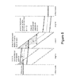
- Figure 5 illustrates energy density due to onset of Fowler-Nordheim tunneling.
- Figure 6 shows a calculation of the density of states (DOS) of Li 3 PO 4 and Li 3 PO 4-x N x that shows that these materials.
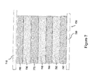
- Figure 7 shows one version of the devices that includes electrodes and multiple layers of dielectric material separated by layers of blocking material.
- Figure 8 illustrates a device 800 that includes first and second electrodes, a dielectric layer disposed between them, and first and second blocking layers.
- Figure 9 illustrates breakdown voltage of energy storage devices.
- Figure 10 is a graph illustrating performance of an exemplary energy storage device with SiO 2 as dielectric material and PZT as blocking material according to embodiments of the present invention.
- blocking layers are provided between dielectric material and the electrodes of an energy storage device.
- the block layers are characterized by higher dielectric constant than the dielectric material.
- Capacitive energy storage has well-known advantages versus electrochemical energy storage, e.g. in a battery. Compared to batteries, capacitors are able to store energy with very high power density, i.e. charge/recharge rates, have long shelf life with little degradation, and can be charged and discharged (cycled) hundreds of thousands or millions of times. However, capacitors often do not store energy in as little volume or weight as in a battery, or at low cost per energy stored, making capacitors impractical for applications such as in electric vehicles. Accordingly, it would be an advance in energy storage technology to provide a capacitive energy storage capable of storing energy more densely per volume and/or mass.
- FIG 2 shows exemplary current voltage curves for a capacitive energy storage device.
- V the voltage across the electrodes
- Q the charge stored on the electrodes
- V max the maximum voltage
- Total Energy ⁇ 0 Qmax ⁇ V Q d Q
- the capacitance, C is equal to the area of electrodes, A, times the permittivity, ⁇ , of the dielectric material divided by the distance between the electrodes, d.
- the energy density of a device may be increased by increasing the permittivity of the dielectric material and/or by increasing the maximum field sustainable in the dielectric material.
- Capacitive energy storage has been limited by the relatively low field strengths sustainable in conventional high permittivity dielectric materials as shown in Figure 3 , which shows the permittivity and breakdown field strength of a number of common dielectrics.
- the dotted line on Figure 3 indicates that the energy density of standard dielectric materials is limited to about 3 Wh/L.
- FIG. 4 shows one version of a high energy density energy storage device described herein.
- the device (400) includes first and second electrodes (410 & 420) spaced apart and a dielectric layer (430) disposed between the electrodes.
- the device also includes blocking layer (440) disposed between the first electrode and the dielectric layer and blocking layer (450) disposed between the second electrode and the dielectric layer.
- the blocking layers, 440 and 450 are made of materials with higher dielectric constant than that of the material of the dielectric layer.
- the blocking layers, 440 and 450 may be the same material or may be different materials.
- the dielectric layer is also referred to as the "low-k material” and the blocking layers is also referred to as the "high-k material.”
- the designations "high” and “low” indicate the relative magnitudes of the dielectric constants of the materials not their absolute values.
- the structure shown in Figure 4 has increased breakdown tolerance, and hence higher energy density, because of the suppression by the blocking layers of injection of charge carriers from the electrodes into the dielectric material.
- this device may have high energy density because the onset of Fowler-Nordheim (FN) tunneling from the electrodes into the dielectric material is delayed to higher voltages.
- the delay of FN tunneling results from the scarcity of charge carriers at the low-k material interface.
- Figure 5 shows that the area B is larger than area A. Tunneling probability of an electron at the interface is inversely related exponentially to the area under the potential barrier (from the WKB approximation).
- the area B will be larger, and the probability of detrimental electron tunneling is exponentially lower.
- the double layer has a charge that repels electrons FN tunneling will be further suppressed.
- the leftmost high-k layer in the example above has anion conduction, the anions will create a double layer at the high-k/low-k interface, and this negative charge will repel electrons from this interface.
- the dielectric layer may generally be made of any dielectric material.
- the dielectric layer material has a breakdown field strength of greater than 0.5V/nm. Breakdown field strength is determined by (i) placing a layer of about 50nm thickness of the test material between conductive electrodes one of which is approximately circular with a diameter of 100 ⁇ m and the other of which is larger than the 100 ⁇ m electrode; (ii) applying a linear voltage ramp across the electrodes, ramping up from 0V at a rate of about 0.1V/s; and, (iii) measuring the current flowing between the electrodes as a function of applied voltage. The breakdown voltage is measured at approximately room temperature.
- a typical current-voltage plot is presented in Figure 9 , showing an initial low voltage region (910) and a breakdown region (920).
- the breakdown voltage is calculated as the voltage at which the current is ten times the measured capacitive charging current.
- the capacitive charging current is 10 -10 A
- the breakdown voltage is about 1V (940) at which the current is 10 -9 A.
- the breakdown field strength is calcualted as the breakdown voltage divided by the thickness of the test material, which may be measured by cross-sectional TEM, X-ray reflectometry (XRR) or elipsometry.
- the current fluctuations shown at about 0.8 V (930) are typical of such current-voltage plots and are seen at voltages approaching the breakdown voltage.
- the dielectric layer material has a relative permittivity of less than 15.
- the relative permittivity is measured at approximately room temperature.
- the dielectric layer material has a band gap of greater than 4eV.
- the breakdown field strength, relative permittivity and band gap described in this parapgraph are material properties of the material that may be used for the dielectric layer; they are not the material properties of the composite blocking layer/dielectric layer/blocking layer system.
- dielectric layer materials that may be used include SiO 2 , HfO 2 , Al 2 O 3 , Si 3 N 4 , oxides, nitrides, oxynitrides and fluorides.
- the dielectric layer material is SiO 2 , HfO 2 , Al 2 O 3 or S 13 N 4 .
- the blocking layer may generally be made of any material having a dielectric constant greater than that of the dielectric constant of the dielectric layer material.
- the blocking layer material has a breakdown field strength of between 1mV/nm and 200mV/nm.
- the blocking layer material has a relative permittivity of greater than 100.
- the blocking layer material has a band gap of less than 4eV.
- the blocking layer material is ionically conducting, has an relative permittivity of greater than 100 and a band gap of greater than 3eV.
- the breakdown field strength, relative permittivity and band gap described in this paragraph are material properties of the material that may be used for the bloxking layer; they are not the material properties of the composite blocking layer/dielectric layer/blocking layer system.
- the blocking layer material may be an ionically conducting material or a non-ionically conducting material.
- the material derives its permittivity at least in part from ion migration within the material, establishing double layers at each interface. These double layers may be engineered to further deplete the electron concentration at the interface to delay the onset of FN tunneling, as is described in Figure 5 .
- the ionically conducting material is an anion conductor.
- the ionically conducting material is a cation conductor.
- the ionically conducting material is a Li + , H + , Na + , O 2- or F - conductor.
- the ionically conducting material is a Li + ion conductor.
- the ionically conducting material Li 3 PO 4 or Li 3 PO 4-x N x As used in this patent application, LiPON means Li 3 PO 4-x N x .
- Figure 6 shows a calculation of the density of states (DOS) of Li 3 PO 4 and Li 3 PO 4-x N x that shows that these materials, along with having a high relative permittivity, have a high bandgap, further delaying the onset of FN tunneling.
- the first blocking layer is an anion conducting material and the second blocking layer is a cation conducting material.
- one or both of the blocking layers comprises an anion conducting material and a cation conducting material.
- a device (800) includes first and second electrodes (810 & 820), a dielectric layer (830) disposed between them and first and second blocking layers (840 & 850) disposed between the dielectric layer and the first and second electrodes respectively.
- the first and second blocking layers include anion conducting material (860 & 880) and cation conducting material (870 & 890).
- only one of the first or second blocking layers includes both cation and anion conducting materials and the other blocking layer includes either a non-ionically conducting material or a cation or anion conducting material.
- the anion conducting material is proximate to the electrode and in other versions of the devices the cation conducting material is proximate to the electrode.
- the material derives its permittivity at least in part from the intrinsic polarizability of the material.
- the non-ionically conducting material is a high-k ceramic material.
- the non-ionically conducting material is a ferroelectric perovskite.
- the non-ionically conducting material is PZT (Pb(Zr 0.5 Ti 0.5 )O 3 ).
- the non-ionically conducting material is SrTiO 3 , PbTiO 3 , BaTiO 3 or (BaSr)TiO 3 .
- the non-ionically conducting material is a multiferroic high k material.
- the non-ionically conducting material is CaCu 3 Ti 4 O 12 or La 2-x Sr x NiO 4 .
- the non-ionically conducting material is a nanocomposite high-k material.
- the blocking layer material has a higher dielectric constant than that of the dielectric layer material.
- the dielectric constant of the blocking layer rmaterial is between 10 and 10000 times greater than the dielectric constant of the dielectric layer rmaterial. In another version the dielectric constant of the blocking layer rmaterial is between 100 and 1000 times greater than the dielectric constant of the dielectric layer rmaterial.
- the electrodes may generally be made of any conducting material that is compatible with the materials of the device with which they have contact.
- the electrodes may, independently, be made of Pt, Cu, Al, Ag or Au.
- the eletrodes may be of the same or different materials.
- the eletrodes have different work functions.
- the electrode that is positively biased during charge has a work function that is lower than that of the work function of the electrode that is negatively biased during charge.
- the electrode that is positively biased during charge has a work function of less than 4.5eV.
- the electrode that is negatively biased during charge has a work function of greater than 4.0eV.
- the blocking layer may generally be of any thickness that maintains the charge carrier injection supression function of the layer. In one version the blocking layer has a thickness of between 4 nm and 100 nm.
- the dielectric layer may generally be of any thickness that maximizes energy storage density while maintaining an insulating property under high field. In one version the dielectric layer has a thickness of between 20 nm and 10 ⁇ m. As shown in the calculation below it may be advantageous for the dielectric layer to be thicker than the blocking layers. In one version the dielectric layer is between 1 and 1000 times the thickness of the blocking layer.
- Figure 7 shows one version of the devices that includes electrodes 710 and 720 and multiple layers of dielectric material (730, 740, 750) separated by layers of blocking material (760, 770, 780, 790).
- Laminate devices In one version of the devices, the dielectric and blocking layers are laminate layers in direct contact with each other with the architectures shown in Figures 4 , 7 and 8 and as otherwise described herein. In other versions the devices include one or more interfacial layers between one or more of the electrodes, dielectric layer and blocking layers.
- a device as described herein has an energy density of between 5 and 1000 Whr/kg. In another version a device as described herein has an energy density of between 10 and 650 Whr/kg. In another version a device as described herein has an energy density of between 50 and 500 Whr/kg. In another version a device as described herein has an energy density of greater than 50 Whr/kg. As used herein, energy density if the energy density at the device level; i.e., the total energy stored in the device divided by the mass of the device.
- the devices described herein may be fabricated in a number of ways, for example using sputtering, PVD, ALD or CVD.
- the devices are fabricated by sputtering using an Endura 5500, 200mm by Applied Materials.
- laminate devices are fabricated by sequential deposition of the blocking layers, dielectric layer(s) and electrodes on a substrate.
- a substrate is not required and the blocking layers, dielectric layer(s) and electrode layer(s) may be deposited directly on to one of the electrodes.
- the devices described herein may generally be used in any application requiring energy storage.
- the devices may be particularly well suited for use in applications such as in electric vehicles, hybrid electric vehicles and grid storage and regulation.
- Devices may be made with the following dielectric and blocking layers
- the devices described herein may have high breakdown strength because a) FN tunneling is not dominant, (for example, calculations suggest that other failure mechanisms in SiO 2 limit the breakdown tolerance to ⁇ 20V/nm) b) the low-k material is intrinsically a high breakdown material (for example, because of high purity, low defect concentration, high bandgap, etc.) c) the electric field is dropped primarily in the low-k material, which has high breakdown strength d) by interleaving thin nano-layers of the low-k material with the high-k material, any free charge carriers in the conduction band may not gain sufficient kinetic energy to cause damage via impact ionization.
- the material under voltage stress may be advantageous for the material under voltage stress have a low defect concentration.
- Defects which introduce states in the middle of the band gap of the insulator can lead to breakdown of the insulator.
- One mechanism by which defects lead to breakdown is that as defects form in a capacitor near the electrode, the field gets concentrated around those defects, enhancing the current around those defects, which leads to heating (and ionization), which results in further defect creation, forming a positive feedback. In the laminate structure, this feedback between defects and current cannot occur, since the material adjacent to the (defective) insulator is not conducting.
- Figure 10 is a graph illustrating performance of an exemplary energy storage device with SiO 2 as dielectric material and PZT as blocking material according to embodiments of the present invention. The graph is generated under the following conditions:
- a stable and substantially uniform electric field is maintained at a about 0.48V/nm.
- the applied electric field is about 0.1.V/nm, and the energy density is about 0.23 Wh/l.
- the high ⁇ region has low field, and low ⁇ region has higher field.
- the applied electric field is 2.2V/nm, the energy density is at about 112Wh/l.
- the blocking layer is characterized by a thickness of 2 nm with 2 nm spacing.
- the applied energy is 0.1V/nm, the energy density is at about 0.095 Wh/l.
- the applied energy is 5.2V/nm, the energy density is at about 257 Wh/l.
- a conductive substrate, or an insulting substrate with a conductive coating forms a first electrode.
- Alternating dielectric and blocking materials are deposited by PVD, sputtering, evaporation, high rate evaporation, close space sublimation, CVD, ALD, PECVD, or solution synthesis such as CBD, precipitation, spray coating, spin coating, roll coating, slot-die, etc.
- SiO 2 may be deposited by sputtering in an Applied Materials Endura 200mm system by reactive RF sputtering of Si in an oxygen plasma.
- LiPON may be deposited in a similar fashion from a Li 3 PO 4 target in a nitrogen plasma.
- One or more stacks of dielectric/blocking layers may be alternated in turn.
- a top electrode may be deposited by a solution process, or a vacuum process, for instance one selected from the list provided above.
- the device may be packaged for reliability and to prevent ingress of oxygen or humidity by any number of techniques common in semiconductor packaging, for example, by alternating layers of parylene and titanium.
- the electrodes are fed through a hermetic seal as common in battery devices.
- any element in a claim that does not explicitly state "means for” performing a specified function, or “step for” performing a specific function, is not to be interpreted as a "means” or “step” clause as specified in 35 U.S.C. Section 112, Paragraph 6.
- the use of "step of” or “act of” in the Claims herein is not intended to invoke the provisions of 35 U.S.C. 112, Paragraph 6.
Abstract
Description
- Described in this patent application are devices for energy storage and methods of making and using such devices.
- In general, a capacitive energy storage device comprises two electrodes with a dielectric material disposed between the electrodes.
Figure 1 is a simplified diagram ilustrating a capacitive energy storage device. As shown inFigure 1 ,dielectric material 103 is positioned between theelectrodes - Unfortunately, conventional energy storage devices are inadequate, as explained below. It is desirable to have new and improved energy storage devices.
- Described in this patent application are devices for energy storage and methods of making and using such devices. In various embodiments, blocking layers are provided between dielectric material and the electrodes of an energy storage device. The block layers are characterized by higher dielectric constant than the dielectric material. There are other embodiments as well.
- In an embodiment, the present invention provides an energy storage device that includes first and second electrodes that are spaced apart. A dielectric layer is disposed between the first and second electrodes. A first blocking layer is disposed between the first electrode and the dielectric layer and a second blocking layer is disposed between the second electrode and the dielectric layer. The dielectric constants of the first and second blocking layers are both independently greater than the dielectric constant of the dielectric layer.
- Depending on the application, the dielectric material may different relative permittivity, which can be between about 2 and 25, between about 3 and 15, or other range. The dielectric layer can have a material characterized by a band gap of greater than 4eV. The dielectric layer can also have a material characterized by a breakdown field strength of greater than 0.5V/nm.
- The dielectric layer may comprise a material selected from oxides, nitrides, oxynitrides and fluorides. The dielectric layer may also comprise a material selected from SiO2, HfO2, Al2O3 or Si3N4.
- The blocking layers, with higher relative dielectric constant, can have a relative permittivity of greater than 20. The material of the block layers can have a band gap of less than 4eV, and the breakdown field strength can be between 1mV/nm and 200mV/nm. Depending on the application, the first and second blocking layers may independently comprise a material selected from ionically conducting materials and non-ionically conducting materials. Depending on the application, the ionically conducting material can be selected from from Li+, H+, Mg2+, Na+, O-, F- conductors, Li3PO4, and Li3PO4-xNx. The non-ionically conducting materials can be multiferroic high k materials, such as CaCu3Ti4O12, La2-xSrxNiO4, nanocomposite high-k materials, high-k ceramic materials, ferroelectric perovskites materials, PZT (Pb(Zr0.5Ti0.5)O3), SrTiO3, PbTiO3, BaTiO3, (BaSr)TiO3, or others.
- The first and second blocking layers independently comprises a material having a dielectric constant between 10 and 10000 times the dielectric constant of the material comprising the dielectric layer. In a specific embodiment, the first and second blocking layers independently comprise a material having a dielectric constant between 50 and 1000 times the dielectric constant of the material comprising the dielectric layer. The first and second blocking layers independently may have a thickness of between 4nm and 100nm. In a specific embodiment, the dielectric layer has a thickness of between 10nm and 10um. The first and second blocking layers independently may have a thickness of between 10 and 1000 times the thickness of the dielectric layer.
- It is to be appreciated that the block layer and dielectric layer material vary depending on the application. In an embodiment, the first and second blocking layers are both PZT and the dielectric layer is SiO2. In another embodiment, the first and second blocking layers are both LiPON and the dielectric layer is SiO2. In another embodiment, the first and second blocking layers are both LiPON and the dielectric layer is Li2O. In yet another embodiment, the first and second blocking layers are both LiPON and the dielectric layer is LiF.
- The blocking layers can also have different material. In an embodiment, the first blocking layer comprises a cation conducting material and the second blocking layer comprises an anion conducting material. In another embodiment, the first blocking layer comprise an anion conducting material and a cation conducting material. In yet another embodiment, the second blocking layer comprise an anion conducting material and a cation conducting material.
- With the structure described above, the device can have an energy density of between 5 and 1000 Whr/kg, an energy density of between 10 and 650 Whr/kg, or an energy density of between 50 and 500 Whr/kg. In certain embodiment, an energy density can greater than 50 Whr/kg, or greater than 100 Whr/kg.
- The first electrode can have a work function greater than the work function of the second electrode. The work function of the first electrode can be greater than 4.0eV and the work function of the second electrode can be less than 4.5eV.
- It is to be appreciated that embodiments of the present invention provides various advantages over conventional techniques. In this patent application, energy storage devices are capable of sustaining higher field strengths than conventional capacitive energy storage devices and which may therefore be used for high energy density capacitive energy storage. More specifically, energy storage devices according to the present invention are capable of withholding higher breakdown voltages (and therefore improved stability and reliability) compared to conventional devices, a thereby allowing a higher level of energy density. There are other benefits as well as described below.
-
Figure 1 is a simplified diagram ilustrating a capacitive energy storage device. -
Figure 2 shows exemplary current voltage curves for a capacitive energy storage device. -
Figure 3 shows the permittivity and breakdown field strength of a number of common dielectrics. -
Figure 4 shows one version of a high energy density energy storage device. -
Figure 5 illustrates energy density due to onset of Fowler-Nordheim tunneling. -
Figure 6 shows a calculation of the density of states (DOS) of Li3PO4 and Li3PO4-xNx that shows that these materials. -
Figure 7 shows one version of the devices that includes electrodes and multiple layers of dielectric material separated by layers of blocking material. -
Figure 8 illustrates adevice 800 that includes first and second electrodes, a dielectric layer disposed between them, and first and second blocking layers. -
Figure 9 illustrates breakdown voltage of energy storage devices. -
Figure 10 is a graph illustrating performance of an exemplary energy storage device with SiO2 as dielectric material and PZT as blocking material according to embodiments of the present invention. - Described in this patent application are devices for energy storage and methods of making and using such devices. In various embodiments, blocking layers are provided between dielectric material and the electrodes of an energy storage device. The block layers are characterized by higher dielectric constant than the dielectric material. There are other embodiments as well.
- Capacitive energy storage has well-known advantages versus electrochemical energy storage, e.g. in a battery. Compared to batteries, capacitors are able to store energy with very high power density, i.e. charge/recharge rates, have long shelf life with little degradation, and can be charged and discharged (cycled) hundreds of thousands or millions of times. However, capacitors often do not store energy in as little volume or weight as in a battery, or at low cost per energy stored, making capacitors impractical for applications such as in electric vehicles. Accordingly, it would be an advance in energy storage technology to provide a capacitive energy storage capable of storing energy more densely per volume and/or mass.
-
Figure 2 shows exemplary current voltage curves for a capacitive energy storage device. Generally the voltage across the electrodes, V, will be some function of the charge stored on the electrodes, Q, as shown in the solid line curve inFigure 2 . There will be some maximum voltage, Vmax, up to which the device can be charged before the dielectric material starts to breakdown. For linear materials the capacitance does not depend on Q and V(Q) =Q/C as shown in the dotted line B inFigure 2 . - The total energy stored in the device is generally given by:

- which for linear materials reduces to:

- The capacitance, C, is equal to the area of electrodes, A, times the permittivity, ε, of the dielectric material divided by the distance between the electrodes, d. The energy density of the device, ρ, can therefore be written as

where Emax is the maximum sustainable field in the dielectric material and is equal to Vmax/d. - As can be seen in
equation 3, the energy density of a device may be increased by increasing the permittivity of the dielectric material and/or by increasing the maximum field sustainable in the dielectric material. Capacitive energy storage has been limited by the relatively low field strengths sustainable in conventional high permittivity dielectric materials as shown inFigure 3 , which shows the permittivity and breakdown field strength of a number of common dielectrics. The dotted line onFigure 3 indicates that the energy density of standard dielectric materials is limited to about 3 Wh/L. - In this patent application are described energy storage devices capable of sustaining higher field strengths than conventional capacitive energy storage devices and which may therefore be used for high energy density capacitive energy storage.
-
Figure 4 shows one version of a high energy density energy storage device described herein. The device (400) includes first and second electrodes (410 & 420) spaced apart and a dielectric layer (430) disposed between the electrodes. The device also includes blocking layer (440) disposed between the first electrode and the dielectric layer and blocking layer (450) disposed between the second electrode and the dielectric layer. The blocking layers, 440 and 450, are made of materials with higher dielectric constant than that of the material of the dielectric layer. The blocking layers, 440 and 450, may be the same material or may be different materials. - In this patent application the dielectric layer is also referred to as the "low-k material" and the blocking layers is also referred to as the "high-k material." The designations "high" and "low" indicate the relative magnitudes of the dielectric constants of the materials not their absolute values.
- Without being bound by theory, it is believed that the structure shown in
Figure 4 has increased breakdown tolerance, and hence higher energy density, because of the suppression by the blocking layers of injection of charge carriers from the electrodes into the dielectric material. As shown inFigure 5 , it is believed that this device may have high energy density because the onset of Fowler-Nordheim (FN) tunneling from the electrodes into the dielectric material is delayed to higher voltages. The delay of FN tunneling results from the scarcity of charge carriers at the low-k material interface.Figure 5 shows that the area B is larger than area A. Tunneling probability of an electron at the interface is inversely related exponentially to the area under the potential barrier (from the WKB approximation). So by increasing the barrier height, the area B will be larger, and the probability of detrimental electron tunneling is exponentially lower. Further, if a double layer is present at the interface, if the double layer has a charge that repels electrons FN tunneling will be further suppressed. For example, if the leftmost high-k layer in the example above has anion conduction, the anions will create a double layer at the high-k/low-k interface, and this negative charge will repel electrons from this interface. - The dielectric layer may generally be made of any dielectric material. In one version of the devices the dielectric layer material has a breakdown field strength of greater than 0.5V/nm. Breakdown field strength is determined by (i) placing a layer of about 50nm thickness of the test material between conductive electrodes one of which is approximately circular with a diameter of 100 µm and the other of which is larger than the 100 µm electrode; (ii) applying a linear voltage ramp across the electrodes, ramping up from 0V at a rate of about 0.1V/s; and, (iii) measuring the current flowing between the electrodes as a function of applied voltage. The breakdown voltage is measured at approximately room temperature. A typical current-voltage plot is presented in
Figure 9 , showing an initial low voltage region (910) and a breakdown region (920). The breakdown voltage is calculated as the voltage at which the current is ten times the measured capacitive charging current. InFigure 9 , for example, if the capacitive charging current is 10-10 A the breakdown voltage is about 1V (940) at which the current is 10-9 A. The breakdown field strength is calcualted as the breakdown voltage divided by the thickness of the test material, which may be measured by cross-sectional TEM, X-ray reflectometry (XRR) or elipsometry. The current fluctuations shown at about 0.8 V (930) are typical of such current-voltage plots and are seen at voltages approaching the breakdown voltage. - In another version of the devices the dielectric layer material has a relative permittivity of less than 15. The relative permittivity is measured by placing a layer of test material of thickness d between two conductive electrodes of area A and scanning the voltage at scan rate s, measuring the capacitive charging current I, and calculating the relative permittivity, ε, as the ratio ε=(I/s)*(d/ε0A). The relative permittivity is measured at approximately room temperature.
- In another version of the devices the dielectric layer material has a band gap of greater than 4eV. The breakdown field strength, relative permittivity and band gap described in this parapgraph are material properties of the material that may be used for the dielectric layer; they are not the material properties of the composite blocking layer/dielectric layer/blocking layer system.
- Specific dielectric layer materials that may be used include SiO2, HfO2, Al2O3, Si3N4, oxides, nitrides, oxynitrides and fluorides. In one version the dielectric layer material is SiO2, HfO2, Al2O3 or S13N4.
- The blocking layer may generally be made of any material having a dielectric constant greater than that of the dielectric constant of the dielectric layer material. In one version of the devices the blocking layer material has a breakdown field strength of between 1mV/nm and 200mV/nm. In another version of the devices the blocking layer material has a relative permittivity of greater than 100. In another version of the devices the blocking layer material has a band gap of less than 4eV. In one version of the device, the blocking layer material is ionically conducting, has an relative permittivity of greater than 100 and a band gap of greater than 3eV. The breakdown field strength, relative permittivity and band gap described in this paragraph are material properties of the material that may be used for the bloxking layer; they are not the material properties of the composite blocking layer/dielectric layer/blocking layer system.
- The blocking layer material may be an ionically conducting material or a non-ionically conducting material.
- In the case of an ionically conducting blocking layer material, the material derives its permittivity at least in part from ion migration within the material, establishing double layers at each interface. These double layers may be engineered to further deplete the electron concentration at the interface to delay the onset of FN tunneling, as is described in
Figure 5 . In one version the ionically conducting material is an anion conductor. In one version the ionically conducting material is a cation conductor. In one version the ionically conducting material is a Li+, H+, Na+, O2- or F- conductor. In one version the ionically conducting material is a Li+ ion conductor. In one version the ionically conducting material Li3PO4 or Li3PO4-xNx. As used in this patent application, LiPON means Li3PO4-xNx.Figure 6 shows a calculation of the density of states (DOS) of Li3PO4 and Li3PO4-xNx that shows that these materials, along with having a high relative permittivity, have a high bandgap, further delaying the onset of FN tunneling. In one version of the devices, the first blocking layer is an anion conducting material and the second blocking layer is a cation conducting material. - In one version of the devices, one or both of the blocking layers comprises an anion conducting material and a cation conducting material. An example of such device is shown in
Figure 8 in which a device (800) includes first and second electrodes (810 & 820), a dielectric layer (830) disposed between them and first and second blocking layers (840 & 850) disposed between the dielectric layer and the first and second electrodes respectively. The first and second blocking layers include anion conducting material (860 & 880) and cation conducting material (870 & 890). In other versions, only one of the first or second blocking layers includes both cation and anion conducting materials and the other blocking layer includes either a non-ionically conducting material or a cation or anion conducting material. In some version of the devices, independently for the first and second blocking layers the anion conducting material is proximate to the electrode and in other versions of the devices the cation conducting material is proximate to the electrode. - In the case of a non-ionically conducting blocking layer material, the material derives its permittivity at least in part from the intrinsic polarizability of the material. In one version the non-ionically conducting material is a high-k ceramic material. In one version the non-ionically conducting material is a ferroelectric perovskite. In another version the non-ionically conducting material is PZT (Pb(Zr0.5Ti0.5)O3). In another version the non-ionically conducting material is SrTiO3, PbTiO3, BaTiO3 or (BaSr)TiO3. In another version the non-ionically conducting material is a multiferroic high k material. In another version the non-ionically conducting material is CaCu3Ti4O12 or La2-xSrxNiO4. In another version the non-ionically conducting material is a nanocomposite high-k material.
- As described above, the blocking layer material has a higher dielectric constant than that of the dielectric layer material. In one version of the devices, the dielectric constant of the blocking layer rmaterial is between 10 and 10000 times greater than the dielectric constant of the dielectric layer rmaterial. In another version the dielectric constant of the blocking layer rmaterial is between 100 and 1000 times greater than the dielectric constant of the dielectric layer rmaterial.
- The electrodes may generally be made of any conducting material that is compatible with the materials of the device with which they have contact. In one version the electrodes may, independently, be made of Pt, Cu, Al, Ag or Au. The eletrodes may be of the same or different materials. In one version, the eletrodes have different work functions. In one version the electrode that is positively biased during charge has a work function that is lower than that of the work function of the electrode that is negatively biased during charge. In one version the electrode that is positively biased during charge has a work function of less than 4.5eV. In one version the electrode that is negatively biased during charge has a work function of greater than 4.0eV.
- The blocking layer may generally be of any thickness that maintains the charge carrier injection supression function of the layer. In one version the blocking layer has a thickness of between 4 nm and 100 nm. The dielectric layer may generally be of any thickness that maximizes energy storage density while maintaining an insulating property under high field. In one version the dielectric layer has a thickness of between 20 nm and 10µm. As shown in the calculation below it may be advantageous for the dielectric layer to be thicker than the blocking layers. In one version the dielectric layer is between 1 and 1000 times the thickness of the blocking layer.
- Calculations have shown that the energy is primarily stored in the material of low-k, as illustrated by the following example:
-
High k material Low k material Material permittivity 800 4 Breakdown Field V/nm 0.1 20 Max absolute voltage V 20000 - Material density g/cm3 5 2.65 -
Thickness [nm] Voltage drop [V] Field [V/nm] Energy [Wh/L] Energy [Wh/kg] High k layer 1 50 5.0 0.10 9.8 Low k layer 1.00E+03 19990.0 19.99 1964.7 High k layer 250 5.0 0.10 9.8 Total 1100 20000 1787.0 624.0 - The above example illustrates that energy densities exceeding those in state-of-the-art batteries may be achieved with such devices.
- Multiple layer devices:
Figure 7 shows one version of the devices that includeselectrodes - Laminate devices: In one version of the devices, the dielectric and blocking layers are laminate layers in direct contact with each other with the architectures shown in
Figures 4 ,7 and8 and as otherwise described herein. In other versions the devices include one or more interfacial layers between one or more of the electrodes, dielectric layer and blocking layers. - Energy Density: In one version a device as described herein has an energy density of between 5 and 1000 Whr/kg. In another version a device as described herein has an energy density of between 10 and 650 Whr/kg. In another version a device as described herein has an energy density of between 50 and 500 Whr/kg. In another version a device as described herein has an energy density of greater than 50 Whr/kg. As used herein, energy density if the energy density at the device level; i.e., the total energy stored in the device divided by the mass of the device.
- Making of the devices: The devices described herein may be fabricated in a number of ways, for example using sputtering, PVD, ALD or CVD. In one method of making described herein, the devices are fabricated by sputtering using an Endura 5500, 200mm by Applied Materials. In one version of the devices, laminate devices are fabricated by sequential deposition of the blocking layers, dielectric layer(s) and electrodes on a substrate. In one version, a substrate is not required and the blocking layers, dielectric layer(s) and electrode layer(s) may be deposited directly on to one of the electrodes.
- Uses of the devices: The devices described herein may generally be used in any application requiring energy storage. The devices may be particularly well suited for use in applications such as in electric vehicles, hybrid electric vehicles and grid storage and regulation.
-
Example Dielectric Layer Material First Blocking Layer Material Second Blocking Layer Material 1 SiO2 PZT PZT 2 SiO2 LiPON LiPON 3 Li2 O LiPON LiPON 4 LiF UPON LiPON 5 SiO2 LiPON YSZ (yttria-stabilized zirconia, (Y2O3)x(ZrO2)1-x - In one version of the energy storage devices described herein the high energy density capacitive energy storage materials may have one or more of the following characteristics:
- 1) Inhibit the onset of Fowler-Nordheim tunneling
- 2) Provide high breakdown strength
- 3) Are tolerant of defects arising during fabrication or during high voltage stress
- In one version, the devices described herein may have high breakdown strength because a) FN tunneling is not dominant, (for example, calculations suggest that other failure mechanisms in SiO2 limit the breakdown tolerance to ∼20V/nm) b) the low-k material is intrinsically a high breakdown material (for example, because of high purity, low defect concentration, high bandgap, etc.) c) the electric field is dropped primarily in the low-k material, which has high breakdown strength d) by interleaving thin nano-layers of the low-k material with the high-k material, any free charge carriers in the conduction band may not gain sufficient kinetic energy to cause damage via impact ionization.
- To increase high voltage breakdown strength, it may be advantageous for the material under voltage stress have a low defect concentration. Defects which introduce states in the middle of the band gap of the insulator can lead to breakdown of the insulator. One mechanism by which defects lead to breakdown is that as defects form in a capacitor near the electrode, the field gets concentrated around those defects, enhancing the current around those defects, which leads to heating (and ionization), which results in further defect creation, forming a positive feedback. In the laminate structure, this feedback between defects and current cannot occur, since the material adjacent to the (defective) insulator is not conducting.
-
Figure 10 is a graph illustrating performance of an exemplary energy storage device with SiO2 as dielectric material and PZT as blocking material according to embodiments of the present invention. The graph is generated under the following conditions: - • Matrix is modeled as "PZT", ε =400
- PZT Edens=0.5*400* ε0*0.1 V/nm=4.9 Wh/l - • blocking layer is modeled as SiO2, ε =3.9, which is 0.5 nm with 2.0 nm spacing
- As illustrated in the graph of
Figure 10 , through the thickness of the blocking material, a stable and substantially uniform electric field is maintained at a about 0.48V/nm. When the applied electric field is about 0.1.V/nm, and the energy density is about 0.23 Wh/l. The high ε region has low field, and low ε region has higher field. When the applied electric field is 2.2V/nm, the energy density is at about 112Wh/l. - In an exemplary embodiment, the blocking layer is characterized by a thickness of 2 nm with 2 nm spacing. When the applied energy is 0.1V/nm, the energy density is at about 0.095 Wh/l. When the applied energy is 5.2V/nm, the energy density is at about 257 Wh/l.
- The following description is presented to enable one of ordinary skill in the art to make and use the invention and to incorporate it in the context of particular applications. Various modifications, as well as a variety of uses in different applications will be readily apparent to those skilled in the art, and the general principles defined herein may be applied to a wide range of embodiments. Thus, the present invention is not intended to be limited to the embodiments presented, but is to be accorded the widest scope consistent with the principles and novel features disclosed herein.
- Numerous methods of fabrication of a device as described herein will be obvious to one skilled in the art. As a non-limiting example, one fabrication sequence is generically described below. A conductive substrate, or an insulting substrate with a conductive coating, forms a first electrode. Alternating dielectric and blocking materials are deposited by PVD, sputtering, evaporation, high rate evaporation, close space sublimation, CVD, ALD, PECVD, or solution synthesis such as CBD, precipitation, spray coating, spin coating, roll coating, slot-die, etc. For example, SiO2 may be deposited by sputtering in an Applied Materials Endura 200mm system by reactive RF sputtering of Si in an oxygen plasma. LiPON may be deposited in a similar fashion from a Li3PO4 target in a nitrogen plasma. One or more stacks of dielectric/blocking layers may be alternated in turn. A top electrode may be deposited by a solution process, or a vacuum process, for instance one selected from the list provided above. The device may be packaged for reliability and to prevent ingress of oxygen or humidity by any number of techniques common in semiconductor packaging, for example, by alternating layers of parylene and titanium. The electrodes are fed through a hermetic seal as common in battery devices.
- The reader's attention is directed to all papers and documents which are filed concurrently with this specification and which are open to public inspection with this specification, and the contents of all such papers and documents are incorporated herein by reference. All the features disclosed in this specification, (including any accompanying claims, abstract, and drawings) may be replaced by alternative features serving the same, equivalent or similar purpose, unless expressly stated otherwise. Thus, unless expressly stated otherwise, each feature disclosed is one example only of a generic series of equivalent or similar features.
- Furthermore, any element in a claim that does not explicitly state "means for" performing a specified function, or "step for" performing a specific function, is not to be interpreted as a "means" or "step" clause as specified in 35 U.S.C. Section 112,
Paragraph 6. In particular, the use of "step of" or "act of" in the Claims herein is not intended to invoke the provisions of 35 U.S.C. 112,Paragraph 6. - Please note, if used, the labels left, right, front, back, top, bottom, forward, reverse, clockwise and counter clockwise have been used for convenience purposes only and are not intended to imply any particular fixed direction. Instead, they are used to reflect relative locations and/or directions between various portions of an object.
- While the above is a full description of the specific embodiments, various modifications, alternative constructions and equivalents may be used. Therefore, the above description and illustrations should not be taken as limiting the scope of the present invention which is defined by the appended claims.
Claims (15)
- An energy storage device comprising first and second electrodes spaced apart, a dielectric layer disposed between the first and second electrodes, a first blocking layer disposed between the first electrode and the dielectric layer and a second blocking layer disposed between the second electrode and the dielectric layer, wherein the dielectric constants of the first and second blocking layers are both independently greater than the dielectric constant of the dielectric layer.
- The device of claim 1, wherein the dielectric layer comprises a material having a relative permittivity of between 2 and 25 or 3 and 15.
- The device of claims 1 or 2, wherein the dielectric layer comprises a material having a breakdown field strength of greater than 0.5V/nm.
- The device of claims 1, 2 or 3, wherein the dielectric layer comprises a material selected from oxides, nitrides, oxynitrides and fluorides, and wherein the dielectric layer comprises a material selected from SiO2, SiOxNy, HfO2, Al2O3 or Si3N4.
- The device of any preceding claim, wherein the first and second blocking layers independently comprises a material having a breakdown field strength of between 1mV/nm and 200mV/nm.
- The device of any preceding claim, wherein the first and second blocking layers independently comprise a material selected from ionically conducting materials and non-ionically conducting materials, and wherein the ionically conducting materials are selected from Mg2+, Li+, H+, Na+, O- and F- conductors, and the ionically conducting materials are Li3PO4 or Li3PO4-xNx, and the non-ionically conducting materials are high-k ceramic materials, multiferroic high k materials, ferroelectric perovskites materials, or nanocomposite high-k materials.
- The device of claim 6, wherein the non-ionically conducting materials are selected from PZT (Pb(Zr0.5Ti0.5)O3), SrTi03, PbTiO3, BaTiO3, (BaSr)TiO3, CaCu3Ti4O12 or La2-xSrxNiO4.
- The device of any preceding claim, wherein the first and second blocking layers independently comprises a material having a dielectric constant between 10 and 10000 times the dielectric constant of the material comprising the dielectric layer.
- The device of any preceding claim, wherein the first and second blocking layers independently have a thickness of between 4nm and 100nm.
- The device of any preceding claim, wherein the dielectric layer has a thickness of between 10nm and 10um.
- The device of any of claims 1 to 8, wherein the first and second blocking layers independently have a thickness of between 10 and 1000 times the thickness of the dielectric layer.
- The device of any preceding claim, wherein the first blocking layer comprises a cation conducting material and the second blocking layer comprises an anion conducting material.
- The device of any of claims 1 to 11, wherein the first blocking layer comprise an anion conducting material and a cation conducting material and the second blocking layer comprise an anion conducting material and a cation conducting material.
- The device of claim 13, wherein the device has an energy density of between 50 and 500 Whr/kg, an energy density of greater than 50 Whr/kg, or energy density of greater than 100 Whr/kg.
- The device of any preceding claim, wherein the first electrode has a work function greater than the work function of the second electrode, and wherein the work function of the first electrode is greater than 4.0eV and the work function of the second electrode is less than 4.5eV.
Applications Claiming Priority (1)
| Application Number | Priority Date | Filing Date | Title |
|---|---|---|---|
| US201261592517P | 2012-01-30 | 2012-01-30 |
Publications (1)
| Publication Number | Publication Date |
|---|---|
| EP2620962A1 true EP2620962A1 (en) | 2013-07-31 |
Family
ID=47750419
Family Applications (1)
| Application Number | Title | Priority Date | Filing Date |
|---|---|---|---|
| EP20130153146 Withdrawn EP2620962A1 (en) | 2012-01-30 | 2013-01-29 | Solid state energy storage devices |
Country Status (3)
| Country | Link |
|---|---|
| US (2) | US9087645B2 (en) |
| EP (1) | EP2620962A1 (en) |
| CN (1) | CN103227048B (en) |
Cited By (1)
| Publication number | Priority date | Publication date | Assignee | Title |
|---|---|---|---|---|
| EP3549189A4 (en) * | 2016-12-02 | 2019-11-20 | Capacitor Sciences Incorporated | Multilayered electrode and film energy storage device |
Families Citing this family (24)
| Publication number | Priority date | Publication date | Assignee | Title |
|---|---|---|---|---|
| US8940850B2 (en) | 2012-08-30 | 2015-01-27 | Carver Scientific, Inc. | Energy storage device |
| US9011627B2 (en) | 2007-10-05 | 2015-04-21 | Carver Scientific, Inc. | Method of manufacturing high permittivity low leakage capacitor and energy storing device |
| EP2206130B1 (en) | 2007-10-05 | 2018-05-09 | Carver Scientific, Inc. | High permittivity low leakage capacitor and energy storing device and method for forming the same |
| US10056609B2 (en) | 2011-07-11 | 2018-08-21 | Quantumscape Corporation | Solid state energy storage devices |
| US9087645B2 (en) | 2012-01-30 | 2015-07-21 | QuantrumScape Corporation | Solid state energy storage devices |
| US10199165B2 (en) | 2012-08-30 | 2019-02-05 | Carver Scientific, Inc. | Energy storage device |
| US9805869B2 (en) | 2012-11-07 | 2017-10-31 | Carver Scientific, Inc. | High energy density electrostatic capacitor |
| KR20170005821A (en) | 2014-05-12 | 2017-01-16 | 캐패시터 사이언시스 인코포레이티드 | Capacitor and method of production thereof |
| US10347423B2 (en) | 2014-05-12 | 2019-07-09 | Capacitor Sciences Incorporated | Solid multilayer structure as semiproduct for meta-capacitor |
| US10340082B2 (en) | 2015-05-12 | 2019-07-02 | Capacitor Sciences Incorporated | Capacitor and method of production thereof |
| MX2016014825A (en) | 2014-05-12 | 2017-03-10 | Capacitor Sciences Inc | Energy storage device and method of production thereof. |
| MX2017005427A (en) | 2014-11-04 | 2017-06-21 | Capacitor Sciences Inc | Energy storage devices and methods of production thereof. |
| BR112017018189A2 (en) | 2015-02-26 | 2018-04-17 | Capacitor Sciences Inc | self-regenerative capacitor and production methods |
| US9932358B2 (en) | 2015-05-21 | 2018-04-03 | Capacitor Science Incorporated | Energy storage molecular material, crystal dielectric layer and capacitor |
| US9941051B2 (en) | 2015-06-26 | 2018-04-10 | Capactor Sciences Incorporated | Coiled capacitor |
| US10026553B2 (en) | 2015-10-21 | 2018-07-17 | Capacitor Sciences Incorporated | Organic compound, crystal dielectric layer and capacitor |
| US11095129B2 (en) * | 2016-02-12 | 2021-08-17 | Capacitor Sciences Incorporated | Capacitor based power system and unmanned vehicle with the capacitor based power system thereof |
| US10305295B2 (en) | 2016-02-12 | 2019-05-28 | Capacitor Sciences Incorporated | Energy storage cell, capacitive energy storage module, and capacitive energy storage system |
| US9978517B2 (en) | 2016-04-04 | 2018-05-22 | Capacitor Sciences Incorporated | Electro-polarizable compound and capacitor |
| US10153087B2 (en) | 2016-04-04 | 2018-12-11 | Capacitor Sciences Incorporated | Electro-polarizable compound and capacitor |
| SG10201912363TA (en) | 2016-12-02 | 2020-02-27 | Carver Scientific Inc | Memory device and capacitive energy storage device |
| RU2764662C1 (en) | 2018-03-12 | 2022-01-19 | ОМЕГА ЭНЕРДЖИ СИСТЕМЗ, ЭлЭлСи | Solid-state energy accumulator from suboxides of transition metals |
| WO2021097051A1 (en) | 2019-11-13 | 2021-05-20 | Omega Energy Systems, Llc | Three-electrode solid-state energy harvester of transition metal suboxides |
| CN112080732B (en) * | 2020-07-29 | 2021-12-28 | 西安交通大学 | Silicon integrated BT-BMZ film, capacitor and manufacturing method thereof |
Citations (3)
| Publication number | Priority date | Publication date | Assignee | Title |
|---|---|---|---|---|
| US20050161717A1 (en) * | 2004-01-28 | 2005-07-28 | Fujitsu Limited | Semiconductor device and method of fabricating the same |
| US20080160712A1 (en) * | 2006-12-27 | 2008-07-03 | Hynix Semiconductor Inc. | Multiple-layer dielectric layer and method for fabricating capacitor including the same |
| US20080277761A1 (en) * | 2007-05-08 | 2008-11-13 | Texas Instruments, Inc. | On-chip isolation capacitors, circuits therefrom, and methods for forming the same |
Family Cites Families (20)
| Publication number | Priority date | Publication date | Assignee | Title |
|---|---|---|---|---|
| CA849697A (en) * | 1970-08-18 | General Electric Company | Capacitor with ionic conducting ceramic electrolyte | |
| FR2601812B1 (en) | 1986-07-21 | 1988-11-25 | Atesys Sa | ELECTRIC CAPACITOR FOR HIGH TEMPERATURES |
| US5471364A (en) * | 1993-03-31 | 1995-11-28 | Texas Instruments Incorporated | Electrode interface for high-dielectric-constant materials |
| US5905000A (en) | 1996-09-03 | 1999-05-18 | Nanomaterials Research Corporation | Nanostructured ion conducting solid electrolytes |
| JP2002075783A (en) * | 2000-08-25 | 2002-03-15 | Alps Electric Co Ltd | Thin-film capacitor for compensating temperature |
| US20030118897A1 (en) * | 2001-02-15 | 2003-06-26 | Shinji Mino | Solid electrolyte cell and production method thereof |
| KR100541551B1 (en) * | 2003-09-19 | 2006-01-10 | 삼성전자주식회사 | Analog capacitor having at least 3 layers of high-k dielectric layers and method of fabricating the same |
| JP2008544936A (en) * | 2005-05-12 | 2008-12-11 | ジョージア テック リサーチ コーポレイション | Coated metal oxide nanoparticles and method for producing the same |
| US7643714B2 (en) | 2005-06-28 | 2010-01-05 | California Institute Of Technology | Nanophotonic devices in silicon |
| US8377586B2 (en) * | 2005-10-05 | 2013-02-19 | California Institute Of Technology | Fluoride ion electrochemical cell |
| US7532083B2 (en) | 2006-03-23 | 2009-05-12 | Intel Corporation | Active nonlinear transmission line |
| US7830644B2 (en) * | 2007-03-05 | 2010-11-09 | Northop Grumman Systems Corporation | High dielectric capacitor materials and method of their production |
| US20110110015A1 (en) * | 2007-04-11 | 2011-05-12 | The Penn State Research Foundation | Methods to improve the efficiency and reduce the energy losses in high energy density capacitor films and articles comprising the same |
| KR20090051634A (en) * | 2007-11-19 | 2009-05-22 | 삼성전자주식회사 | Capacitor and method of manufacturing the capacitor |
| US20110275005A1 (en) | 2008-10-24 | 2011-11-10 | Nanosys, Inc | Membrane Electrode Assemblies With Interfacial Layer |
| EP2387793A1 (en) | 2009-01-16 | 2011-11-23 | The Board of Trustees of The Leland Stanford Junior University | Quantum dot ultracapacitor and electron battery |
| US10056609B2 (en) | 2011-07-11 | 2018-08-21 | Quantumscape Corporation | Solid state energy storage devices |
| US8541282B2 (en) * | 2011-11-07 | 2013-09-24 | Intermolecular, Inc. | Blocking layers for leakage current reduction in DRAM devices |
| US20130143087A1 (en) * | 2011-12-01 | 2013-06-06 | Applied Nanostructured Solutions, Llc. | Core/shell structured electrodes for energy storage devices |
| US9087645B2 (en) | 2012-01-30 | 2015-07-21 | QuantrumScape Corporation | Solid state energy storage devices |
-
2013
- 2013-01-25 US US13/749,706 patent/US9087645B2/en active Active
- 2013-01-29 CN CN201310034515.9A patent/CN103227048B/en active Active
- 2013-01-29 EP EP20130153146 patent/EP2620962A1/en not_active Withdrawn
-
2015
- 2015-04-29 US US14/700,048 patent/US9293255B2/en active Active
Patent Citations (3)
| Publication number | Priority date | Publication date | Assignee | Title |
|---|---|---|---|---|
| US20050161717A1 (en) * | 2004-01-28 | 2005-07-28 | Fujitsu Limited | Semiconductor device and method of fabricating the same |
| US20080160712A1 (en) * | 2006-12-27 | 2008-07-03 | Hynix Semiconductor Inc. | Multiple-layer dielectric layer and method for fabricating capacitor including the same |
| US20080277761A1 (en) * | 2007-05-08 | 2008-11-13 | Texas Instruments, Inc. | On-chip isolation capacitors, circuits therefrom, and methods for forming the same |
Cited By (1)
| Publication number | Priority date | Publication date | Assignee | Title |
|---|---|---|---|---|
| EP3549189A4 (en) * | 2016-12-02 | 2019-11-20 | Capacitor Sciences Incorporated | Multilayered electrode and film energy storage device |
Also Published As
| Publication number | Publication date |
|---|---|
| US20130194716A1 (en) | 2013-08-01 |
| US20150235768A1 (en) | 2015-08-20 |
| US9293255B2 (en) | 2016-03-22 |
| CN103227048A (en) | 2013-07-31 |
| CN103227048B (en) | 2017-06-23 |
| US9087645B2 (en) | 2015-07-21 |
Similar Documents
| Publication | Publication Date | Title |
|---|---|---|
| US9293255B2 (en) | Solid state energy storage devices | |
| US9646766B2 (en) | Method of making dielectric capacitors with increased dielectric breakdown strength | |
| US10741334B2 (en) | Method and associated capacitors having engineered electrodes with very high energy density | |
| US9178006B2 (en) | Methods to improve electrical performance of ZrO2 based high-K dielectric materials for DRAM applications | |
| US9111681B2 (en) | Thin film capacitor | |
| US11145665B2 (en) | Electrical storage device with negative capacitance | |
| US20070121274A1 (en) | Small volume thin film and high energy density crystal capacitors | |
| US8481384B2 (en) | Method for producing MIM capacitors with high K dielectric materials and non-noble electrodes | |
| US7084482B2 (en) | Capacitor of a semiconductor device and memory device using the same | |
| CN113168932B (en) | Dielectric structure for electrical insulation using vacuum or gas | |
| US11417724B2 (en) | Capacitor including perovskite material, semiconductor device including the capacitor, and method of manufacturing the capacitor | |
| CN116458282A (en) | Four layer high K for metal-insulator-metal capacitors | |
| US10867749B2 (en) | Multilayer capacitor | |
| US10446324B2 (en) | Thin film capacitor | |
| Smitha et al. | Annealing effects on capacitance density and voltage coefficient of capacitance (VCC) of thin-film capacitor for energy harvesting application | |
| WO2022219939A1 (en) | Capacitor, electric circuit, circuit board, electronic apparatus, and power storage device | |
| US20060170073A1 (en) | Capacitor with high breakdown field | |
| US20230207201A1 (en) | Dielectric composition and multilayer capacitor | |
| US20230215635A1 (en) | Dielectric composition and multilayer capacitor | |
| Park et al. | Electrical Charateristics of ZrO₂-Al₂O₃-ZrO₂ Laminated Capacitor via Changes of Bottom Electrode-Alumina Distances | |
| Sahoo et al. | ZrO2 Layer Thickness and Field Dependent Leakage Current in Ba0. 8Sr0. 2TiO3/ZrO2 Heterostructured Thin Films |
Legal Events
| Date | Code | Title | Description |
|---|---|---|---|
| PUAI | Public reference made under article 153(3) epc to a published international application that has entered the european phase |
Free format text: ORIGINAL CODE: 0009012 |
|
| AK | Designated contracting states |
Kind code of ref document: A1 Designated state(s): AL AT BE BG CH CY CZ DE DK EE ES FI FR GB GR HR HU IE IS IT LI LT LU LV MC MK MT NL NO PL PT RO RS SE SI SK SM TR |
|
| AX | Request for extension of the european patent |
Extension state: BA ME |
|
| 17P | Request for examination filed |
Effective date: 20131210 |
|
| RBV | Designated contracting states (corrected) |
Designated state(s): AL AT BE BG CH CY CZ DE DK EE ES FI FR GB GR HR HU IE IS IT LI LT LU LV MC MK MT NL NO PL PT RO RS SE SI SK SM TR |
|
| 17Q | First examination report despatched |
Effective date: 20140515 |
|
| STAA | Information on the status of an ep patent application or granted ep patent |
Free format text: STATUS: EXAMINATION IS IN PROGRESS |
|
| STAA | Information on the status of an ep patent application or granted ep patent |
Free format text: STATUS: THE APPLICATION IS DEEMED TO BE WITHDRAWN |
|
| 18D | Application deemed to be withdrawn |
Effective date: 20170124 |