EP2549654A1 - Low-consumption logic circuit and integrated circuit comprising at least one such logic circuit - Google Patents
Low-consumption logic circuit and integrated circuit comprising at least one such logic circuit Download PDFInfo
- Publication number
- EP2549654A1 EP2549654A1 EP12177104A EP12177104A EP2549654A1 EP 2549654 A1 EP2549654 A1 EP 2549654A1 EP 12177104 A EP12177104 A EP 12177104A EP 12177104 A EP12177104 A EP 12177104A EP 2549654 A1 EP2549654 A1 EP 2549654A1
- Authority
- EP
- European Patent Office
- Prior art keywords
- voltage
- switches
- logic circuit
- supply voltage
- logic
- Prior art date
- Legal status (The legal status is an assumption and is not a legal conclusion. Google has not performed a legal analysis and makes no representation as to the accuracy of the status listed.)
- Withdrawn
Links
Images


Classifications
-
- H—ELECTRICITY
- H03—ELECTRONIC CIRCUITRY
- H03K—PULSE TECHNIQUE
- H03K19/00—Logic circuits, i.e. having at least two inputs acting on one output; Inverting circuits
- H03K19/0008—Arrangements for reducing power consumption
- H03K19/0019—Arrangements for reducing power consumption by energy recovery or adiabatic operation
-
- H—ELECTRICITY
- H03—ELECTRONIC CIRCUITRY
- H03K—PULSE TECHNIQUE
- H03K19/00—Logic circuits, i.e. having at least two inputs acting on one output; Inverting circuits
- H03K19/02—Logic circuits, i.e. having at least two inputs acting on one output; Inverting circuits using specified components
Definitions
- the present invention relates to a low power logic circuit and to integrated circuits comprising at least one such logic circuit.
- CMOS technology Complementary Metal-Oxide Semiconductor
- adiabatic logic which consists of optimally controlling the charges and discharges of the capabilities of a integrated circuit, these capacities being mainly those interconnection lines which are significantly higher than those of the transistors.
- the adiabatic logic is described in the document WC Athas, "Low power Digital systems based on adiabatic switching principles", IEEE transactions on VLSI systems VOL 2, N04 December 1994 .
- FIG. 1A we can see a logic inverter in conventional CMOS technology.
- the logic inverter comprises a transistor p and a transistor n 102, 104.
- G, S and D respectively denote the gate, the source and the drain of the transistors.
- a and its complement designate the control signals.
- figure 1C shows how to perform any logic function according to the inputs, the associated circuit being a combination of transistors in series or in parallel.
- the inverter function is simply performed by a transistor, a PMOS for F and an NMOS for the complementary function.
- the resistor R is the sum of the resistances between the power supply and the input of the interconnection line (resistance of the switch used + resistances of the connection lines).
- Q is the load stored in the capacity of the interconnection line (in fact this capacity plus the input capacity of the next stage but generally much lower).
- the constant current of charge and discharge is i.
- the voltage to be established on the interconnection line is the supply voltage (the load being assumed almost total).
- T is the time during which the interconnection line is charged or discharged.
- the circuits proposed to date are based on a linear variation of the voltage power during the operations of charging and discharging capabilities which amounts to the first order to work at constant current.
- the case of the inverter allows to specify this mode of operation.
- the supply voltage is no longer constant as in conventional logic, but is established relatively slowly at each change of state.
- the inputs (input) are positioned and then the supply voltage V power supply is gradually brought to the nominal voltage V DD for a time T, thereby to establish the output level then transmit this level on these doors.
- the opposite operation is then performed to reset the system and process another logical event.
- the supply voltage V alim is then relatively slowly lowered from V DD to zero.
- the inputs are then also brought to zero potential waiting for a new state change.
- the figure 1D represents a logical function equivalent to that of the figure 1C performed in adiabatic logic.
- the trapezoidal shape of the power signal is often replaced by a sinusoidal or sinusoidal signal which is easier to generate and constitutes a suitable approximation.
- E R ⁇ VS The T ⁇ VS The ⁇ V DD 2 + 1 2 ⁇ VS The ⁇ V T 2
- Such mechanical switches do not have a threshold voltage in the semiconductor sense.
- a very small value of the applied voltage is sufficient to pass a current without having to cross a threshold voltage.
- they have negligible static dissipation in contrast to transistors. Therefore the dissipated energy is reduced compared to that dissipated by the CMOS.
- the combination of mechanical switches with electrostatic actuation and adiabatic logic makes it possible to obtain an integrated circuit of which the energy dissipated is at first order independent of the supply voltage, which allows for low consumption circuits without the need to implement very low supply voltages.
- the operating voltage can be chosen freely which avoids having to work at very low voltages like CMOS.
- a gap between 5 nm and 100 nm between the mobile structure and the base in the switches can be implemented.
- the present invention has the advantage of not being the seat of leakage current. In adiabatic logic, it is then possible to arbitrarily choose the operating frequency which is impossible with MOS, since it is necessary to achieve a static energy-dynamic energy compromise which leads to an optimal operating frequency.
- the mechanical switches do not have a threshold voltage which leads to the elimination of non-adiabatic residues in the dissipation, unlike the MOS switches which lead to terms depending on the square of the threshold voltage.
- the supply voltage source is variable according to at least three successive phases, a first phase of increasing the voltage from a zero value to a nominal voltage, a second phase of maintaining the voltage of supply at the nominal voltage and a third phase of reducing the supply voltage of the nominal voltage to a zero value, and at least two mechanical switches, said switches being microelectromechanical switches or nanoelectromechanical switches, and switching means of said switches .
- each switch comprises two electrical conductive tracks, one of which is connected to the supply voltage source and a moving part intended to come into contact with the two tracks in a state of closure of the switch, and the switching means using a control voltage to move the moving part.
- the switching means are of the electrostatic type and comprise a fixed electrode facing at least part of the moving part and means for applying the positive control voltage to attract the mobile part towards the electrode. fixed and put in contact the moving part with the conductive tracks.
- the supply voltage is equal to the control voltage.
- the duration of the first phase is between 1 and 100 ns, and the nominal supply voltage can be between 100 mV and 10 V.
- the switching means are of the magnetic or piezoelectric type.
- the logic circuit according to the invention may be a logic inverter or a NON OR or NON AND or AND or OR circuit or a Toffoli gate or a Fredkin gate or a Feynman gate.
- the present invention also relates to an integrated circuit comprising at least a first and a second logic circuit according to the present invention.
- the output voltage of the first gate controlling the second gate.
- These logic gates include, instead of transistors mechanical switches, more particularly nanointer switches or microswitches made by NEMS (Nanoelectromechanical Systems) or MEMS (Microelectromechanical Systems).
- NEMS Nanoelectromechanical Systems
- MEMS Microelectromechanical Systems
- the closing and sometimes the opening of these switches can be controlled by electrostatic means, by application of a magnetic field, by piezoelectric effect, by thermal effect, etc.
- the capacitors 6, 8 of capacity C L symbolize the capacities of the interconnection lines.
- the designated supply voltage V power supply is input of the two mechanical switches 2, 4.
- the door of the figure 2 operates in adiabatic logic, ie the source of supply voltage is such that it can charge and discharge at almost constant current an interconnection line through the mechanical switches.
- the voltage supply source is such that the voltage "V alim supply is not constant and varies in a trapezoidal profile.
- the variation of the voltage V power supply is shown schematically in figures 2 and 3 .
- the supply voltage progressively increases from 0 until reaching the nominal voltage V DD , during a time T, which makes it possible to establish the output level and then transmit this level to the following gates.
- the power supply voltage V power supply is maintained for a while at the rated voltage V DD and then, during a third phase III, the supply voltage V alim decreases during the time T to give the system to zero and deal with another logical event. The inputs are then also brought to zero potential waiting for a new state change.
- the voltage increase time and the voltage decrease time are preferably substantially equal.
- the time during which the voltage is constant is substantially constant.
- the trapezoidal profile is approximated by a half-sinusoid.
- the energy stored in the interconnection capacity is not discharged to the ground as in the CMOS logic which introduces necessarily a dissipation, but towards the food which served to load it. A large part of the energy is therefore recovered by the power supply.
- Adiabatic logic is also called energy recovery logic.
- the switch is intended to electrically connect two tracks 10, 12 made on the surface of the integrated circuit, the switch comprises a connection means formed by a movable portion 14 provided with a control electrode 15 disposed above the two tracks. 10, 12 and a fixed electrode 16 on the fixed portion 11 of the integrated circuit and at least a portion of which is opposite the movable portion 14.
- the movable portion 14 is of the cantilever type. It could be formed by a membrane.
- the two tracks 10, 12 are aligned and have two free ends 10.1, 12.1 respectively opposite, the fixed electrode 16 is located between the free ends 10.1, 12.1 of the two tracks 10, 12, and the part Mobile 14 overlaps the two ends 10.1, 12.1 of the tracks 10, 12 and is perpendicular to the fixed electrode.
- the moving part 14 is, in the absence of positive voltage applied, between the movable portion 14 and the fixed electrode 16 held suspended above the tracks by elastic elements beams type. When a sufficient control voltage is applied, the moving part approaches the tracks under the effect of the electric force and comes into contact therewith so as to ensure the electrical connection therewith.
- the mobile part is of the lever type (or “cantilever" in English terminology ").
- the switch structure shown on the Figures 4, 5A and 5B is only an example of embodiment and is in no way limiting.
- a magnetic actuation switch is shown on the Figures 6A and 6B it comprises a movable part 514 of the cantilever type and the control means are formed by a permanent magnet 524 and a coil 526 separated by a substrate 528.
- the movable part 614 is also of the cantilever type, it comprises two portions 630, 632 of piezoelectric material, for example AIN, the application of a positive voltage V causes for one an expansion 630 in the plane and for the other 632 a contraction, closing the switch, and conversely the application of a negative voltage V causes for one 630 a contraction and the other an expansion 632, opening the switch.
- the switch structures represented on the Figures 6A to 7B are examples of embodiments and are in no way limiting.
- FIG. 3A and 3B examples of embodiments of NON OR gates made according to the present invention can be seen.
- the door has two branches fed by parallel V alim, one having two switches in series 210, 212 and the other comprising two parallel switches 220, 222.
- Each arm is loaded by its own capacity C L.
- a C L capacity is provided between the two switches in series and the switches in parallel. Also represented are the voltages V across A and B.
- the switches may be similar to those shown on the Figures 4, 5A and 5B .
- the door comprises two switches 310, 312 in parallel carrying out the commands A and B, in series with two switches in parallel 320, 322 carrying out the commands and B complemented.
- the voltage source is connected to the switches 310, 312.
- a capacitor C L is provided between the two switches in series and the switches in parallel.
- the switches 310 and 312 are open, the switches 320 and 322 are closed.
- the complemented control A and the complemented control B can be replaced by commands A and B with different switches, ie closed without application of control voltage and opened by application of a control voltage.
- FIG. 3C an example of a NAN gate according to the present invention can be seen using four mechanical switches 410, 412, 420, 422. Also shown are the voltages V across A and B.
- switches of the same logic circuit are similar or identical in order to simplify the construction and control of the circuit.
- the inverter according to the present invention consumes energy only during switching, this consumption is referred to as dynamic consumption, its static consumption being negligible.
- the switch is conductive regardless of the voltage value applied between the two conductive tracks 10, 12 and as low a voltage is transmitted between the input and the exit.
- the current flowing between the two tracks is independent of the control voltage value, unlike a CMOS switch in which the current between the source and the drain depends on the value of the threshold voltage.
- the closing of the mechanical switch is effective from a certain control voltage value, however it is not comparable to the threshold voltage of a MOS transistor because its value does not affect the value current flowing through the switch and therefore does not introduce dynamic non-adiabatic consumption.
- the control electrode being electrically insulated, there is no static consumption.
- E Mecca R Mecca ⁇ VS The T ⁇ VS The ⁇ V DD 2
- C L the capacity of the interconnections
- R meca the electrical resistance of interconnections and contacts
- E MOS R mos ⁇ VS The T ⁇ VS The ⁇ V DD 2 + VS The ⁇ V T 2
- R meca can be as weak as 1000 Ohms for a voltage V DD of 1 V.
- the rise time T of the polarization signal can be chosen at 10 ns.
- connection line The typical capacity of the connection line is 10 fF.
- the threshold voltage of an advanced CMOS technology in low power consumption is of the order of 300 mV.
- the threshold voltage of the CMOS technology can not be reduced because of the static consumption and since it is possible to envisage voltages of a few volts for the supply voltage V DD , it can be seen that the logic circuit according to the invention makes it possible to reduce the energy dissipated by a factor of the order of 100 relative to a logic circuit in advanced CMOS technology.
- This factor would be between 100 and 1000 for a time T of 100 ns.
- a high supply voltage also makes it possible to solve the problem of bonding the mechanical switches.
- control voltage V is also the nominal output or supply voltage, its value is therefore V DD , which makes it possible to simplify the architecture of the entire integrated circuit, since a logic gate in command another. Otherwise the output voltage of a logic gate would be transformed so that it forms a control voltage of another logic gate.
- the time taken by the structure to contact the substrate when a voltage is applied can also be calculated as a function of the applied voltage and the characteristics of the switch. This time should be less than the T time chosen in classical logic architectures and therefore should be a few nanoseconds if T is 10 ns.
- the miniaturization of mechanical switches could lead to such values.
- logical architectures more adapted to mechanical switches however allow to relax this constraint for example by performing more complex logical functions at the level of the elementary doors.
- T is advantageously between 1 and 100 ns.
- This value would be 75 kTa for a value of T of 100 ns.
- the examples of logic gates represented on the figures 2 and 3 are in no way limiting and apply to any type of logical gate architecture.
- the NOR gate has been given as an example but the classic NAND, AND and OR doors are also feasible according to this principle. It is the same for the functions obtained by combining elementary gates (adders, registers, SRAM or DRAM memory cell). It should also be noted that the doors used in the reversible calculation (Fredkin doors, of Toffoli and Feynman) are also feasible according to this principle.
- the logic circuits thus produced are particularly suitable for applications requiring a very low consumption, for example portable autonomous systems.
- the present invention is also particularly suitable for systems with a high degree of "parallelization", i.e. systems having a large number of circuits operating at relatively slow frequencies, thus requiring rather low block operating frequencies.
- circuits according to the present invention can be made by conventional microelectronics technologies used to produce MEMS OR NEMS systems, for example by silicon technology, by deposition and etching of layer, but any other technology making it possible to produce miniaturized mechanical switches is applicable.
Landscapes
- Physics & Mathematics (AREA)
- Engineering & Computer Science (AREA)
- Computer Hardware Design (AREA)
- Computing Systems (AREA)
- General Engineering & Computer Science (AREA)
- Mathematical Physics (AREA)
- Logic Circuits (AREA)
- Semiconductor Integrated Circuits (AREA)
Abstract
Description
La présente invention se rapporte à un circuit logique à faible consommation et à des circuits intégrés comportant au moins un tel circuit logique.The present invention relates to a low power logic circuit and to integrated circuits comprising at least one such logic circuit.
Les circuits logiques de l'état de la technique sont réalisés en technologie CMOS ("Complementary Metal-Oxide Semiconductor" en terminologie anglo-saxonne) qui associe une paire de transistors complémentaires, l'un de type N, l'autre de type P, sur un même support.The logic circuits of the state of the art are made in CMOS technology ("Complementary Metal-Oxide Semiconductor") which associates a pair of complementary transistors, one of the N type and the other of the P type. , on the same support.
En particulier à cause du développement des systèmes électroniques autonomes, on cherche à contrôler la consommation des circuits intégrés afin de la réduire. Plusieurs solutions peuvent être mises en oeuvre, l'une consiste à réduire la tension d'alimentation des circuits, en effet la consommation dite dynamique est proportionnelle au carré de cette tension, l'autre solution consiste à favoriser la mise en oeuvre de plusieurs circuits fonctionnant à des fréquences relativement lentes par rapport à un système fonctionnant à fréquence élevée. Cependant ces solutions présentent des limites liées à la réduction de taille de transistors.Especially because of the development of autonomous electronic systems, it seeks to control the consumption of integrated circuits to reduce it. Several solutions can be implemented, one consists in reducing the supply voltage of the circuits, in fact the so-called dynamic consumption is proportional to the square of this voltage, the other solution is to favor the implementation of several circuits. operating at relatively slow frequencies compared to a system operating at a high frequency. However, these solutions have limits related to the size reduction of transistors.
Il existe une autre solution appelée logique adiabatique qui consiste à contrôler de manière optimale les charges et décharges des capacités d'un circuit intégré, ces capacités étant principalement celles des lignes d'interconnexion qui sont nettement supérieures à celles des transistors. La logique adiabatique est décrite dans le document
Sur la
Dans la logique classique, à chaque changement d'état, la capacité CL des lignes d'interconnexion est chargée à la tension d'alimentation VDD puis déchargée à la masse. Une énergie est donc dissipée thermiquement qui peut s'écrire pour un cycle : 
On peut montrer de manière théorique que pour minimiser l'énergie dissipée par effet Joule dans la résistance en série avec une capacité, il faut garantir que les opérations de charge et de décharge s'effectuent à courant constant. Dans ce cas il est facile de montrer que l'énergie dissipée pendant le temps T pendant lequel on charge ou on décharge la capacité s'écrit : 
La résistance R est la somme des résistances entre l'alimentation et l'entrée de la ligne d'interconnexion (résistance de l'interrupteur utilisé + résistances des lignes de connexion). Pour établir ce résultat, Il suffit de résoudre le système d'équations : ![]()
![]()

![]()
![]()
Q est la charge stockée dans la capacité de la ligne d'interconnexion (en fait cette capacité plus la capacité d'entrée de l'étage suivant mais en général beaucoup plus faible).Q is the load stored in the capacity of the interconnection line (in fact this capacity plus the input capacity of the next stage but generally much lower).
Le courant constant de charge et de décharge est i.The constant current of charge and discharge is i.
La tension à établir sur la ligne d'interconnexion est la tension d'alimentation (la charge étant supposée quasi-totale).The voltage to be established on the interconnection line is the supply voltage (the load being assumed almost total).
T est le temps pendant lequel on charge ou on décharge la ligne d'interconnexion.T is the time during which the interconnection line is charged or discharged.
En pratique, pour se rapprocher de cette condition idéale, les circuits proposés à ce jour sont basés sur une variation linéaire de la tension d'alimentation pendant les opérations de charge et de décharge des capacités ce qui revient au premier ordre à travailler à courant constant. Le cas de l'inverseur permet de préciser ce mode de fonctionnement.In practice, to get close to this ideal condition, the circuits proposed to date are based on a linear variation of the voltage power during the operations of charging and discharging capabilities which amounts to the first order to work at constant current. The case of the inverter allows to specify this mode of operation.
En logique adiabatique, dans le cas de l'inverseur représenté sur la
La
Le plus souvent les portes adiabatiques réalisent aussi la fonction complémentaire comme il est indiqué sur les
Dans la mesure où la capacité CL est chargée et déchargée lentement par rapport à la constante de temps typique du circuit RCL, R étant la résistance globale associée au processus de charge et de décharge, qui inclut la résistance de sortie du ou des transistors réalisant les fonctions F ainsi que la résistance des connexions, la tension aux bornes de la capacité CL peut suivre la tension appliquée en entrée. La tension aux bornes de la résistance est donc quasi nulle et la consommation thermique peut donc être réduite de manière importante par rapport à la logique classique.Since the capacity C L is slowly loaded and discharged with respect to the typical time constant of the RC circuit L , where R is the overall resistance associated with the charging and discharging process, which includes the output resistance of the transistor (s) performing the F functions as well as the resistance of the connections, the voltage at the terminals of the capacity C L can follow the applied voltage input. The voltage across the resistor is therefore almost zero and the thermal consumption can therefore be reduced significantly compared to conventional logic.
L'énergie dissipée lors de la charge peut alors s'écrire comme dans le cas idéal de la charge à courant constant : 
Lors de la décharge une énergie équivalente est dissipée.During the discharge equivalent energy is dissipated.
Par conséquent l'énergie dissipée en logique adiabatique peut être réduite de manière importante à condition que la période T soit très supérieure aux constantes de temps RCL.Therefore the energy dissipated in adiabatic logic can be significantly reduced provided that the period T is much greater than the time constants RC L.
En pratique, la forme en trapèze du signal d'alimentation est souvent remplacée par un signal sinusoïdal ou en partie sinusoïdal plus facile à générer et constituant une approximation convenable.In practice, the trapezoidal shape of the power signal is often replaced by a sinusoidal or sinusoidal signal which is easier to generate and constitutes a suitable approximation.
Cette logique n'a cependant donné lieu à aucune réalisation industrielle. En effet, le calcul exposé ci-dessus ignore une caractéristique des transistors réalisés dans une technologie à base de semi-conducteurs à savoir l'effet de seuil. Pour rendre le transistor (ou les transistors) conducteurs dans la phase de charge ou de décharge des capacités, il faut que la tension de commande appliquée à la grille dépasse une valeur appelée tension de seuil et notée VT dans la technologie CMOS. En général la tension de commande et la tension d'alimentation sont de même valeur pour simplifier l'architecture. Dans le cas de l'inverseur de la
L'énergie dissipée dans le processus de charge peut s'écrire en première approximation : 
Pour réduire cet effet négatif il faudrait réduire la tension de seuil VT à une valeur proche de 0, mais dans la technologie CMOS cette solution est inapplicable car elle conduirait à une consommation statique non tolérable due au courant sous le seuil. La consommation statique est liée au courant de fuite des transistors (conduction résiduelle en dessous du seuil), elle varie exponentiellement avec la diminution de la tension de seuil et des rapports VT/VDD supérieurs à 0,2 voire 0,3 dans des technologies basse consommation sont nécessaires.To reduce this negative effect it would reduce the threshold voltage V T to a value close to 0, but in CMOS technology this solution is inapplicable because it would lead to a non-tolerable static consumption due to the current below the threshold. The static consumption is related to the leakage current of the transistors (residual conduction below the threshold), it varies exponentially with the decrease of the threshold voltage and V T / V DD ratios greater than 0.2 or even 0.3 in Low power technologies are needed.
Par conséquent, la logique adiabatique théoriquement d'un grand intérêt est incapable de réduire largement la consommation des circuits réalisés dans une technologie d'interrupteurs à base de semi-conducteurs, présentant des effets de seuil.Therefore, the adiabatic logic of great interest is incapable of greatly reducing the consumption of circuits made in a semiconductor-based switch technology with threshold effects.
C'est par conséquent le but de la présente invention d'offrir un circuit logique à consommation d'énergie très faible.It is therefore the object of the present invention to provide a logic circuit with very low power consumption.
Le but précédemment énoncé est atteint par un circuit logique en logique adiabatique ; i.e. alimenté par une source de tension d'alimentation apte à charger et de décharger à courant quasi constant une ligne d'interconnexion à travers des interrupteurs mécaniques, et mettant en oeuvre des interrupteurs microélectromécaniques ou MEMS ou nanoélectromécaniques ou NEMS à la place des transistors N et P.The previously stated goal is reached by a logic circuit in adiabatic logic; ie powered by a supply voltage source capable of charging and discharging at an almost constant current an interconnection line through mechanical switches, and implementing microelectromechanical or MEMS or nanoelectromechanical or NEMS switches in place of the transistors N and P.
D'une part de tels interrupteurs mécaniques ne présentent pas de tension de seuil au sens des semi-conducteurs. Quand le contact est établi, une valeur très petite de la tension appliquée suffit à faire passer un courant sans avoir à franchir une tension de seuil. En outre, ils présentent une dissipation statique négligeable à l'inverse des transistors. Par conséquent l'énergie dissipée est réduite par rapport à celle dissipée par les CMOS.On the one hand, such mechanical switches do not have a threshold voltage in the semiconductor sense. When the contact is established, a very small value of the applied voltage is sufficient to pass a current without having to cross a threshold voltage. In addition, they have negligible static dissipation in contrast to transistors. Therefore the dissipated energy is reduced compared to that dissipated by the CMOS.
D'autre part, de manière particulièrement intéressante, la combinaison d'interrupteurs mécaniques avec une actuation électrostatique et de la logique adiabatique permet d'obtenir un circuit intégré dont l'énergie dissipée est au premier ordre indépendante de la tension d'alimentation, ce qui permet de réaliser des circuits basse consommation sans nécessité de mettre en oeuvre des tensions d'alimentation très faibles. La tension de fonctionnement peut être choisie librement ce qui évite de devoir travailler à des tensions très faibles comme en CMOS.On the other hand, in a particularly interesting way, the combination of mechanical switches with electrostatic actuation and adiabatic logic makes it possible to obtain an integrated circuit of which the energy dissipated is at first order independent of the supply voltage, which allows for low consumption circuits without the need to implement very low supply voltages. The operating voltage can be chosen freely which avoids having to work at very low voltages like CMOS.
Cet effet est complètement inattendu pour l'homme du métier qui associe généralement faible consommation et faible tension d'alimentation.This effect is completely unexpected for those skilled in the art who generally associate low power and low power supply.
Grâce à l'invention, dans le cas de dispositifs ultra basse consommation, il n'est plus nécessaire de réduire la tension d'alimentation, une telle réduction ayant des effets négatifs sur la fiabilité.Thanks to the invention, in the case of ultra low power devices, it is no longer necessary to reduce the supply voltage, such a reduction having negative effects on reliability.
Dans le cas d'un circuit intégré qui mettrait en oeuvre un ou plusieurs interrupteurs mécaniques en logique classique, les tensions d'alimentation devraient être abaissées en dessous de 200 mV pour pouvoir présenter un avantage important par rapport aux circuits intégrés CMOS. Cependant de telles tensions d'alimentation imposeraient des jeux entre la structure mobile et la base de l'interrupteur de l'ordre de quelques nanomètres, ce qui impliquerait de difficultés technologiques de réalisation très considérables.In the case of an integrated circuit that would implement one or more mechanical switches in conventional logic, the supply voltages should be lowered below 200 mV to be able to have a significant advantage over CMOS integrated circuits. However, such supply voltages would impose clearances between the mobile structure and the base of the switch of the order of a few nanometers, which would imply considerable technological difficulties of realization.
Grâce à l'invention, de telles contraintes technologiques sont supprimées. Un jeu compris entre 5 nm et 100 nm entre la structure mobile et le base dans les interrupteurs peut être mis en oeuvre.Thanks to the invention, such technological constraints are removed. A gap between 5 nm and 100 nm between the mobile structure and the base in the switches can be implemented.
Alors que les interrupteurs mécaniques sont considérés par l'homme du métier du domaine des circuits intégrés comme lents, présentant une résistance de contact élevée dans le cas des interrupteurs de petites dimensions et pouvant en outre être sujet à des problèmes de collage, l'inventeur de la présente invention est aller à l'encontre des préjugés sur les interrupteurs mécaniques en les utilisant pour réaliser les portes logiques en logique adiabatique et a obtenu des résultats inattendus de cette combinaison. En particulier, l'indépendance au premier ordre de l'énergie dissipée par rapport à la tension d'alimentation.il en résulte que la tension d'alimentation peut être relativement élevée ce qui procure l'avantage inattendu de résoudre les problèmes de collage, puisque ceux-ci sont notablement réduits lorsque la tension appliquée est faible.While mechanical switches are considered by those skilled in the field of integrated circuits as slow, having a high contact resistance in the case of small switches and may also be subject to gluing problems, the inventor of the present invention is to counter the prejudices on mechanical switches by using them to realize logic gates adiabatic logic and obtained unexpected results of this combination. In particular, the first-order independence of the dissipated energy with respect to the supply voltage. As a result, the supply voltage can be relatively high which provides the unexpected advantage of solving the gluing problems. since these are significantly reduced when the applied voltage is low.
La présente invention présente l'avantage de ne pas être le siège de courant de fuite. En logique adiabatique, il est alors possible de choisir arbitrairement la fréquence de fonctionnement ce qui est impossible avec des MOS, puisqu'il faut atteindre un compromis énergie statique-énergie dynamique ce qui conduit à une fréquence optimale de fonctionnement.The present invention has the advantage of not being the seat of leakage current. In adiabatic logic, it is then possible to arbitrarily choose the operating frequency which is impossible with MOS, since it is necessary to achieve a static energy-dynamic energy compromise which leads to an optimal operating frequency.
En outre, les interrupteurs mécaniques ne présentent pas de tension de seuil ce qui conduit à éliminer les résidus non adiabatiques dans la dissipation, contrairement aux interrupteurs MOS qui conduisent à des termes dépendant du carré de la tension de seuil.In addition, the mechanical switches do not have a threshold voltage which leads to the elimination of non-adiabatic residues in the dissipation, unlike the MOS switches which lead to terms depending on the square of the threshold voltage.
La présente invention a alors pour objet un circuit logique pour circuit intégré comportant :
- une source de tension d'alimentation apte à charger et de décharger à courant quasi constant une ligne d'interconnexion à travers des interrupteurs mécaniques :
- une ligne d'interconnexion,
- des interrupteurs mécaniques, lesdits interrupteurs étant des interrupteurs microélectromécaniques ou des interrupteurs nanoélectromécaniquees,
- des moyens de commutation desdits interrupteurs.
- a source of supply voltage able to charge and discharge at almost constant current an interconnection line through mechanical switches:
- an interconnection line,
- mechanical switches, said switches being microelectromechanical switches or nanoelectromechanical switches,
- switching means of said switches.
Dans un mode avantageux, la source de tension d'alimentation est variable selon au moins trois phases successives, une première phase d'augmentation de la tension d'une valeur nulle à une tension nominale, une deuxième phase de maintien de la tension d'alimentation à la tension nominale et une troisième phase de diminution de la tension d'alimentation de la tension nominale à une valeur nulle, et au moins deux interrupteurs mécaniques lesdits interrupteurs étant des interrupteurs microélectromécaniques ou des interrupteurs nanoélectromécaniquees, et des moyens de commutation desdits interrupteurs.In an advantageous mode, the supply voltage source is variable according to at least three successive phases, a first phase of increasing the voltage from a zero value to a nominal voltage, a second phase of maintaining the voltage of supply at the nominal voltage and a third phase of reducing the supply voltage of the nominal voltage to a zero value, and at least two mechanical switches, said switches being microelectromechanical switches or nanoelectromechanical switches, and switching means of said switches .
Par exemple, chaque interrupteur comporte deux pistes conductrices électriques, dont l'une est connectée à la source de tension d'alimentation et une partie mobile destinée à venir en contact avec les deux pistes dans un état de fermeture de l'interrupteur, et les moyens de commutation mettant en oeuvre une tension de commande pour déplacer la partie mobile.For example, each switch comprises two electrical conductive tracks, one of which is connected to the supply voltage source and a moving part intended to come into contact with the two tracks in a state of closure of the switch, and the switching means using a control voltage to move the moving part.
De manière préférée, les moyens de commutation sont de type électrostatique et comportent une électrode fixe en regard d'une partie au moins de la partie mobile et des moyens d'application de la tension de commande positive pour attirer la partie mobile vers l'électrode fixe et mettre en contact la partie mobile avec les pistes conductrices.Preferably, the switching means are of the electrostatic type and comprise a fixed electrode facing at least part of the moving part and means for applying the positive control voltage to attract the mobile part towards the electrode. fixed and put in contact the moving part with the conductive tracks.
Avantageusement la tension d'alimentation est égale à la tension de commande.Advantageously, the supply voltage is equal to the control voltage.
Par exemple, la durée de la première phase est comprise entre 1 et 100 ns, et la tension d'alimentation nominale peut être comprise entre 100 mV et 10 V.For example, the duration of the first phase is between 1 and 100 ns, and the nominal supply voltage can be between 100 mV and 10 V.
En variante, les moyens de commutation sont de type magnétique ou piézoélectrique.In a variant, the switching means are of the magnetic or piezoelectric type.
Le circuit logique selon l'invention peut être un inverseur logique ou un circuit NON OU ou NON ET ou ET ou OU ou une porte de Toffoli ou une porte de Fredkin ou une porte de Feynman.The logic circuit according to the invention may be a logic inverter or a NON OR or NON AND or AND or OR circuit or a Toffoli gate or a Fredkin gate or a Feynman gate.
La présente invention a également pour objet un circuit intégré comportant au moins un premier et un deuxième circuit logique selon la présente invention.The present invention also relates to an integrated circuit comprising at least a first and a second logic circuit according to the present invention.
Dans un mode de réalisation, la tension de sortie de la première porte commandant la deuxième porte.In one embodiment, the output voltage of the first gate controlling the second gate.
La présente invention sera mieux comprise à l'aide de la description qui va suivre et des dessins joints en annexe sur lesquels :
- les
figures 1A à 1D sont des portes logiques de l'état de la technique, - la
figure 2 est un exemple d'inverseur logique selon la présente invention, - les
figures 3A ,3B et 3C sont des exemples de portes NON OU (ou NOR en terminologie anglo-saxonne) et NON ET (NAND) logiques selon la présente invention, - la
figure 4 est une vue complète d'une représentation schématique d'un interrupteur mécanique pouvant être mis en oeuvre dans la présente invention, - les
figures 5A et 5B sont des vues de côté de l'interrupteur de lafigure 4 dans un état fermé et dans un état ouvert respectivement, - les
figures 6A et 6B sont des vues de dessus et en coupe d'un exemple de réalisation d'un interrupteur mécanique à commande magnétique utilisable dans la présente invention, - les
figures 7A et 7B sont des vues en coupe longitudinale d'un exemple de réalisation d'un interrupteur mécanique à commande piézoélectrique utilisable dans la présente invention, dans un état en cours de fermeture et dans un état ouvert respectivement.
- the
Figures 1A to 1D are logical gates of the state of the art, - the
figure 2 is an example of a logic inverter according to the present invention, - the
Figures 3A ,3B and 3C are examples of NOR gates (or NOR in English terminology) and NAND gates (NAND) according to the present invention, - the
figure 4 is a complete view of a schematic representation of a mechanical switch that can be implemented in the present invention, - the
Figures 5A and 5B are side views of the switch of thefigure 4 in a closed state and in an open state respectively, - the
Figures 6A and 6B are views from above and in section of an exemplary embodiment of a magnetic control mechanical switch used in the present invention, - the
Figures 7A and 7B are views in longitudinal section of an exemplary embodiment of a piezoelectric controlled mechanical switch used in the present invention, in a state being closed and in an open state respectively.
Sur les
Ces portes logiques comportent, en lieu et places des transistors des interrupteurs mécaniques, plus particulièrement des nanointerrupteurs ou microinterrupteurs réalisés par technologie NEMS (Nanoelectromechanical Systems) ou MEMS (Microelectromechanical Systems). La fermeture et parfois l'ouverture de ces interrupteurs peuvent être commandées par des moyens électrostatiques, par application d'un champ magnétique, par effet piézoélectrique, par effet thermique...These logic gates include, instead of transistors mechanical switches, more particularly nanointer switches or microswitches made by NEMS (Nanoelectromechanical Systems) or MEMS (Microelectromechanical Systems). The closing and sometimes the opening of these switches can be controlled by electrostatic means, by application of a magnetic field, by piezoelectric effect, by thermal effect, etc.
A des fins de simplicité, les " nano et microinterrupteurs " seront désignés uniquement par " interrupteurs mécaniques ".For the sake of simplicity, the "nano and micro-switches" will be designated only by "mechanical switches".
Sur le circuit de la
Les condensateurs 6, 8 de capacité CL symbolisent les capacités des lignes d'interconnexion.The
La tension d'alimentation désignée Valim est appliquée en entrée des deux interrupteurs mécaniques 2, 4.The designated supply voltage V power supply is input of the two
Dans le cas d'interrupteurs à commande électrostatique, une tension de commande V assure la fermeture des interrupteurs 2, 4.In the case of electrostatically controlled switches, a control voltage V closes the
Selon l'invention, la porte de la
Par exemple, la source d'alimentation en tension est telle que la tension d"alimentation Valim n'est pas constante et varie selon un profil trapézoïdal. La variation de la tension Valim est représentée schématiquement sur les
Le temps d'augmentation de la tension et le temps de diminution de la tension sont de préférence sensiblement égaux. En outre, le temps pendant lequel la tension est constante est sensiblement constant. En pratique, le profil trapézoïdal est approximé par une demi-sinusoïde.The voltage increase time and the voltage decrease time are preferably substantially equal. In addition, the time during which the voltage is constant is substantially constant. In practice, the trapezoidal profile is approximated by a half-sinusoid.
Dans la logique adiabatique appelée également " logique à récupération d'énergie " (energy recovery logic en anglais), l'énergie stockée dans la capacité de l'interconnexion n'est pas déchargée à la masse comme dans la logique CMOS ce qui introduit nécessairement une dissipation, mais vers l'alimentation qui a servi à la charger. Une grande partie de l'énergie est donc récupérée par l'alimentation. La logique adiabatique est également appelée logique à récupération d'énergie (energy recovery logic en anglais).In the adiabatic logic also called "energy recovery logic" (energy recovery logic), the energy stored in the interconnection capacity is not discharged to the ground as in the CMOS logic which introduces necessarily a dissipation, but towards the food which served to load it. A large part of the energy is therefore recovered by the power supply. Adiabatic logic is also called energy recovery logic.
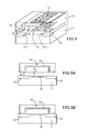
Sur la
L'interrupteur est destiné à connecter électriquement deux pistes 10, 12 réalisées sur la surface du circuit intégré, l'interrupteur comporte un moyen de connexion formé par une partie mobile 14 munie d'une électrode de commande 15 disposée au-dessus des deux pistes 10, 12 et une électrode fixe 16 sur la partie fixe 11 du circuit intégré et dont une partie au moins est en regard de la partie mobile 14. Dans l'exemple représenté, la partie mobile 14 est de type cantilever. Elle pourrait être formée par une membrane.The switch is intended to electrically connect two
Dans l'exemple représenté, les deux pistes 10, 12 sont alignées et comportent deux extrémités libres 10.1, 12.1 respectivement en regard, l'électrode fixe 16 est située entre les extrémités libres 10.1, 12.1 des deux pistes 10, 12, et la partie mobile 14 chevauche les deux extrémités 10.1, 12.1 des pistes 10, 12 et est perpendiculaire à l'électrode fixe.In the example shown, the two
La partie mobile 14 est, en l'absence de tension positive appliquée, entre la partie mobile 14 et l'électrode fixe 16 maintenue suspendue au-dessus des pistes par des éléments élastiques type poutres. Lorsqu'une tension de commande suffisante est appliquée, la partie mobile se rapproche des pistes sous l'effet de la force électrique et entre en contact avec celles-ci de sorte à assurer la connexion électrique avec celle-ci. Par exemple la partie mobile est du type levier (ou "cantilever" en terminologie anglo-saxonne").The moving
Sur la
La structure d'interrupteur représentée sur la
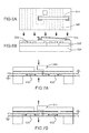
Un interrupteur à actuation magnétique est représenté sur les
Sur les
Les structures d'interrupteur représentées sur les
Sur les
Les interrupteurs peuvent être similaires à ceux représentés sur les
Sur la
Sur la
De préférence tous les interrupteurs d'un même circuit logique sont similaires ou identiques afin de simplifier la réalisation et la commande du circuit.Preferably all the switches of the same logic circuit are similar or identical in order to simplify the construction and control of the circuit.
Nous allons maintenant déterminer l'énergie dissipée pour un interrupteur mécanique à commande électrostatique et dans le cas d'un inverseur logique selon la présente invention.We will now determine the energy dissipated for an electrostatically controlled mechanical switch and in the case of a logic inverter according to the present invention.
L'inverseur selon la présente invention consomme de l'énergie uniquement lors des commutations, cette consommation est désignée consommation dynamique, sa consommation statique étant négligeable.The inverter according to the present invention consumes energy only during switching, this consumption is referred to as dynamic consumption, its static consumption being negligible.
En effet, le contact mécanique étant établi par positionnement des entrées, l'interrupteur est conducteur quelle que soit la valeur de tension appliquée entre les deux pistes conductrices 10, 12 et une tension aussi faible soit-elle est transmise entre l'entrée et la sortie.Indeed, the mechanical contact being established by positioning the inputs, the switch is conductive regardless of the voltage value applied between the two
Le courant circulant entre les deux pistes est indépendant de la valeur de tension de commande, à l'inverse d'un interrupteur CMOS dans lequel le courant entre la source et le drain dépend de la valeur de la tension de seuil. La fermeture de l'interrupteur mécanique est effective à partir d'une certaine valeur de tension de commande, cependant celle-ci n'est pas comparable à la tension de seuil d'un transistor MOS car sa valeur n'intervient pas sur la valeur du courant qui traverse l'interrupteur et n'introduit donc pas de consommation dynamique non adiabatique. De plus l'électrode de commande étant électriquement isolée, il n'y a pas de consommation statique.The current flowing between the two tracks is independent of the control voltage value, unlike a CMOS switch in which the current between the source and the drain depends on the value of the threshold voltage. The closing of the mechanical switch is effective from a certain control voltage value, however it is not comparable to the threshold voltage of a MOS transistor because its value does not affect the value current flowing through the switch and therefore does not introduce dynamic non-adiabatic consumption. In addition, the control electrode being electrically insulated, there is no static consumption.
L'énergie dissipée peut alors s'écrire : 
Avec CL la capacité des interconnexions,
Rmeca la résistance électrique des interconnexions et des contactsThe dissipated energy can then be written:
With C L the capacity of the interconnections,
R meca the electrical resistance of interconnections and contacts
A titre de comparaison, l'énergie de commutation d'un inverseur adiabatique à base de MOS est : 
En supposant que la période T est choisie de telle manière que le premier terme de l'expression (II) dans le cas d'un d'inverseur CMOS soit négligeable, on peut comparer : 
et ![]()
and ![]()
Par exemple, Rmeca peut être aussi faible que 1000 Ohms pour une tension VDD de 1 V.For example, R meca can be as weak as 1000 Ohms for a voltage V DD of 1 V.
Le temps T de montée du signal de polarisation peut être choisi à 10 ns.The rise time T of the polarization signal can be chosen at 10 ns.
La capacité typique de la ligne de connexion est de 10 fF.The typical capacity of the connection line is 10 fF.
La tension de seuil d'une technologie CMOS avancée en faible consommation est de l'ordre de 300 mV.The threshold voltage of an advanced CMOS technology in low power consumption is of the order of 300 mV.
Les deux énergies sont alors CL ·VT 2 pour la CMOS et 10-3 CL ·VDD 2 pour la solution NEMS.The two energies are then C L · V T 2 for CMOS and 10 -3 C L · V DD 2 for the NEMS solution.
Comme cela a été expliqué précédemment, la tension de seuil de la technologie CMOS ne peut être réduite à cause de la consommation statique et comme il est possible d'envisager des tensions de quelques volts pour la tension d'alimentation VDD, on constate que le circuit logique selon l'invention permet de réduire l'énergie dissipée d'un facteur de l'ordre de 100 par rapport à un circuit logique en technologique CMOS avancée.As explained above, the threshold voltage of the CMOS technology can not be reduced because of the static consumption and since it is possible to envisage voltages of a few volts for the supply voltage V DD , it can be seen that the logic circuit according to the invention makes it possible to reduce the energy dissipated by a factor of the order of 100 relative to a logic circuit in advanced CMOS technology.
Par exemple, en prenant des valeurs typiques de 300 mV pour la tension de seuil et de 1 V pour le tension d'alimentation du circuit logique selon l'invention, on obtient un facteur 100.For example, taking typical values of 300 mV for the threshold voltage and 1 V for the supply voltage of the logic circuit according to the invention, a factor of 100 is obtained.
Ce facteur serait entre 100 et 1000 pour un temps T de 100 ns.This factor would be between 100 and 1000 for a time T of 100 ns.
Par conséquent, grâce à l'invention on obtient un circuit logique à basse consommation.Therefore, thanks to the invention we obtain a low power logic circuit.
En outre, grâce à la combinaison d'un fonctionnement en logique adiabatique et d'interrupteurs mécaniques selon l'invention, on peut réaliser des systèmes intégrés à basse consommation sans devoir utiliser des tensions d'alimentation basses. Pouvoir utiliser des tensions relativement hautes (de l'ordre du volt) est un grand avantage car les circuits fonctionnant à tension basse (100 mV ou moins) sont particulièrement sensibles aux perturbations électriques. Le fait d'avoir l'énergie de commutation quasi indépendante de la tension utilisée donne une grande souplesse à la conception des systèmes électroniques. De plus, la possibilité de faire varier la tension d'alimentation dans une vaste plage permet une optimisation plus facile des interrupteurs mécaniques par exemple en éliminant plus facilement les problèmes de collage ou les problèmes de claquage électrique.In addition, thanks to the combination of adiabatic logic operation and mechanical switches according to the invention, it is possible to realize integrated low power systems without having to use low supply voltages. Being able to use relatively high voltages (of the order of a volt) is a great advantage because low voltage circuits (100 mV or less) are particularly sensitive to electrical disturbances. Having the switching energy virtually independent of the voltage used gives great flexibility to the design of electronic systems. In addition, the ability to vary the supply voltage in a wide range allows for easier optimization of mechanical switches for example by eliminating more easily sticking problems or problems of electrical breakdown.
Comme indiqué ci-dessus, une tension d'alimentation élevée permet en outre de résoudre le problème du collage des interrupteurs mécaniques.As indicated above, a high supply voltage also makes it possible to solve the problem of bonding the mechanical switches.
Dans le cas de l'actuation électrostatique, la force F appliquée entre la partie mobile et l'électrode fixe lorsque le contact est établi, s'écrit : 
La résistance de contact se calcule classiquement par la formule de Sharvin : 
- V la tension de commande des interrupteurs de l'inverseur,
- R la résistance du contact entre la partie mobile et les pistes,
- p la résistivité du métal utilisé dans la partie mobile,
- S la surface en regard de l'électrode fixe (
notée 16 sur lafigure 5A ) et de l'électrode correspondante pour la partie mobile, - λ le libre parcours moyen des électrons dans le métal,
- A la surface de contact entre la partie mobile et les pistes,
- g est le jeu à l'état ouvert entre la partie mobile et l'électrode fixe (représenté sur la
figure 5A ), - gd est le jeu, à l'état ouvert, entre la partie mobile et la base au niveau des zones destinées à entrer en contact (représenté sur la
figure 5A ).
- V the control voltage of the inverter switches,
- R the resistance of the contact between the moving part and the tracks,
- p the resistivity of the metal used in the moving part,
- S the surface facing the fixed electrode (noted 16 on the
Figure 5A ) and the corresponding electrode for the moving part, - λ the average free path of the electrons in the metal,
- At the contact surface between the moving part and the tracks,
- g is the clearance in the open state between the moving part and the fixed electrode (shown in FIG.
Figure 5A ) - g d is the clearance, in the open state, between the moving part and the base at the areas intended to come into contact (shown in
Figure 5A ).
Par ailleurs, la surface de contact A peut se calculer comme suit : 
- H étant la dureté du métal
- ξ étant le coefficient d'élasticité de l'ordre de 0,3.
- H being the hardness of the metal
- ξ being the coefficient of elasticity of the order of 0.3.
De manière préférentielle la tension de commande V est aussi la tension de sortie ou d'alimentation nominale, sa valeur est donc VDD, ce qui permet de simplifier l'architecture de l'ensemble du circuit intégré, puisqu'une porte logique en commande une autre. Sinon la tension de sortie d'une porte logique serait transformée afin qu'elle forme une tension de commande d'une autre porte logique.Preferably, the control voltage V is also the nominal output or supply voltage, its value is therefore V DD , which makes it possible to simplify the architecture of the entire integrated circuit, since a logic gate in command another. Otherwise the output voltage of a logic gate would be transformed so that it forms a control voltage of another logic gate.
L'énergie de commutation en logique adiabatique pour une porte étage est alors, en supposant que les résistances de contact sont les contributions principales à la résistance totale ce qui est confirmé par la littérature : 
On constate donc de manière très surprenante que l'énergie dissipée est indépendante de la tension de commande et donc de la tension nominale d'alimentation, contrairement aux préjugés de l'homme du métier qui considère généralement qu'une basse consommation impose une tension d'alimentation faible.It is thus very surprisingly observed that the dissipated energy is independent of the control voltage and therefore of the nominal supply voltage, contrary to the prejudices of the human being. of the trade which generally considers that a low consumption imposes a low supply voltage.
La démonstration précédente s'applique dans le cas des interrupteurs à commande électrostatique. Pour les autres types de commande, il y a également un effet compensateur du même type. En effet, la résistance de contact dépend de l'actuation et donc de la tension de commande, mais pas nécessairement selon une loi inversement proportionnelle au carré de la tension comme dans l'interrupteur à commande électrostatique.The previous demonstration applies in the case of electrostatically controlled switches. For other types of control, there is also a compensating effect of the same type. Indeed, the contact resistance depends on the actuation and therefore the control voltage, but not necessarily according to a law inversely proportional to the square of the voltage as in the electrostatic control switch.
Le temps mis par la structure pour entrer en contact avec le substrat quand une tension est appliquée peut également se calculer en fonction de la tension appliquée et des caractéristiques de l'interrupteur. Ce temps devrait être inférieur au temps T choisi dans des architectures logiques classiques et donc devrait être de quelques nanosecondes si T est de 10 ns. La miniaturisation des interrupteurs mécaniques pourrait conduire à de telles valeurs. Dans tous les cas, des architectures logiques plus adaptées aux interrupteurs mécaniques permettent cependant de relâcher cette contrainte par exemple en réalisant des fonctions logiques plus complexes au niveau des portes élémentaires.The time taken by the structure to contact the substrate when a voltage is applied can also be calculated as a function of the applied voltage and the characteristics of the switch. This time should be less than the T time chosen in classical logic architectures and therefore should be a few nanoseconds if T is 10 ns. The miniaturization of mechanical switches could lead to such values. In all cases, logical architectures more adapted to mechanical switches however allow to relax this constraint for example by performing more complex logical functions at the level of the elementary doors.
Il est alors possible de calculer le rapport entre l'énergie dissipée dans un circuit à base de transistors en logique adiabatique et celle dissipée dans un circuit selon l'invention, ce qui représente le facteur de mérite de l'invention par rapport aux circuits existants.It is then possible to calculate the ratio between the energy dissipated in a circuit based on transistors in adiabatic logic and that dissipated in a circuit according to the invention, which represents the merit factor of the invention compared with existing circuits. .
Ce facteur s'écrit : 
On constate donc que la présente invention a d'autant plus d'intérêt quand T augmente et CL diminue.It is therefore found that the present invention is all the more interesting when T increases and C L decreases.
T est avantageusement compris entre 1 et 100 ns.T is advantageously between 1 and 100 ns.
Le facteur de mérite de l'invention peut s'écrire pour des valeurs typiques des constantes physiques mises en jeux : 
Le facteur de forme de l'interrupteur mécanique est défini par : 
Cette relation donne le domaine d'applicabilité de l'invention. On cherche un facteur de mérite supérieur à 100 pour un facteur de forme donné, 1 000 par exemple.This relationship gives the field of applicability of the invention. We look for a merit factor greater than 100 for a given form factor, for example 1,000.
Des valeurs typiques de 10 fF pour la capacité, de 10 ns pour T et de 200 mV pour la tension de seuil du circuit MOS conduisent à des valeurs de l'ordre de : 
Pour obtenir un gain significatif de 80, le facteur de forme de 1000. Un interrupteur de gap 10 nm avec une surface de commande électrostatique de 300 nm × 300 nm serait compatible ce qui conduit à un encombrement raisonnable.To obtain a significant gain of 80, the form factor of 1000. A 10 nm gap switch with an electrostatic control surface 300 nm × 300 nm would be compatible which leads to a reasonable size.
Reprenons la valeur théorique de l'énergie dissipée pour une actuation électrostatique. 
Pour une capacité d'interconnexion de 10, 10-15 F et pour une valeur de T égale à 10 ns, on obtient pour des dispositifs à couche métallique en exprimant l'énergie en kTa comme il est fréquent dans le domaine de la faible consommation. 
k étant la constante de Boltzmann.
Ta étant la température absolue en Kelvin Une valeur de 750 kTa est donc possible pour F égal à 1000 ce qui est exceptionnel comparé à la CMOS.For an interconnection capacity of 10, 10 -15 F and for a value of T equal to 10 ns, we obtain for metal-layer devices by expressing the energy in kTa as it is frequent in the field of low consumption. .
k being the Boltzmann constant.
Ta is the absolute temperature in Kelvin A value of 750 kTa is therefore possible for F equal to 1000 which is exceptional compared to CMOS.
Cette valeur serait de 75 kTa pour une valeur de T de 100 ns.This value would be 75 kTa for a value of T of 100 ns.
Les exemples de portes logiques représentés sur les
Les circuits logiques ainsi réalisés sont particulièrement adaptés à des applications requérant une consommation très faible, par, exemple les systèmes autonomes portables.The logic circuits thus produced are particularly suitable for applications requiring a very low consumption, for example portable autonomous systems.
La présente invention est également particulièrement adaptée à des systèmes à haut degré de " parallélisation ", i.e. des systèmes comportant un grand nombre de circuits fonctionnant à des fréquences relativement lentes, donc demandant des fréquences de fonctionnement par bloc assez faibles.The present invention is also particularly suitable for systems with a high degree of "parallelization", i.e. systems having a large number of circuits operating at relatively slow frequencies, thus requiring rather low block operating frequencies.
Les circuits selon la présente invention peuvent être réalisés par les technologies classiques de la microélectronique utilisées pour réaliser les systèmes MEMS OU NEMS, par exemple par une technologie silicium, par dépôt et gravure de couche mais toute autre technologie permettant de réaliser des interrupteurs mécaniques miniaturisés est applicable.The circuits according to the present invention can be made by conventional microelectronics technologies used to produce MEMS OR NEMS systems, for example by silicon technology, by deposition and etching of layer, but any other technology making it possible to produce miniaturized mechanical switches is applicable.
Claims (12)
Applications Claiming Priority (1)
| Application Number | Priority Date | Filing Date | Title |
|---|---|---|---|
| FR1156670A FR2978311B1 (en) | 2011-07-22 | 2011-07-22 | LOW CONSUMPTION LOGIC CIRCUIT AND INTEGRATED CIRCUIT COMPRISING AT LEAST ONE SUCH LOGIC CIRCUIT |
Publications (1)
| Publication Number | Publication Date |
|---|---|
| EP2549654A1 true EP2549654A1 (en) | 2013-01-23 |
Family
ID=46507935
Family Applications (1)
| Application Number | Title | Priority Date | Filing Date |
|---|---|---|---|
| EP12177104A Withdrawn EP2549654A1 (en) | 2011-07-22 | 2012-07-19 | Low-consumption logic circuit and integrated circuit comprising at least one such logic circuit |
Country Status (3)
| Country | Link |
|---|---|
| US (1) | US8982528B2 (en) |
| EP (1) | EP2549654A1 (en) |
| FR (1) | FR2978311B1 (en) |
Cited By (2)
| Publication number | Priority date | Publication date | Assignee | Title |
|---|---|---|---|---|
| EP2838199A1 (en) * | 2013-08-14 | 2015-02-18 | Commissariat à l'Énergie Atomique et aux Énergies Alternatives | Logic circuit with low-consumption mechanical switches |
| EP3182590A1 (en) * | 2015-12-18 | 2017-06-21 | Commissariat À L'Énergie Atomique Et Aux Énergies Alternatives | Low-power logic cell |
Families Citing this family (3)
| Publication number | Priority date | Publication date | Assignee | Title |
|---|---|---|---|---|
| JP2015213994A (en) * | 2014-05-12 | 2015-12-03 | 国立大学法人東北大学 | Digital circuit utilizing nano-mechanical switch |
| US10432197B2 (en) * | 2016-08-08 | 2019-10-01 | Qualcomm Incorporated | Electronic devices employing adiabatic logic circuits with wireless charging |
| FR3069742B1 (en) * | 2017-07-25 | 2019-10-25 | Commissariat A L'energie Atomique Et Aux Energies Alternatives | CAPACITIVE LOGIC CELL |
Citations (4)
| Publication number | Priority date | Publication date | Assignee | Title |
|---|---|---|---|---|
| US5638946A (en) * | 1996-01-11 | 1997-06-17 | Northeastern University | Micromechanical switch with insulated switch contact |
| US6153839A (en) * | 1998-10-22 | 2000-11-28 | Northeastern University | Micromechanical switching devices |
| US20020153583A1 (en) * | 2000-11-09 | 2002-10-24 | Frazier Gary A. | Nanomechanical switches and circuits |
| US20050253571A1 (en) * | 2004-05-12 | 2005-11-17 | University Of Florida Research Foundation, Inc. | MEMS waveform generator and adiabatic logic circuits using the same |
Family Cites Families (2)
| Publication number | Priority date | Publication date | Assignee | Title |
|---|---|---|---|---|
| US7106066B2 (en) * | 2002-08-28 | 2006-09-12 | Teravicta Technologies, Inc. | Micro-electromechanical switch performance enhancement |
| US7164744B2 (en) * | 2004-06-18 | 2007-01-16 | Nantero, Inc. | Nanotube-based logic driver circuits |
-
2011
- 2011-07-22 FR FR1156670A patent/FR2978311B1/en not_active Expired - Fee Related
-
2012
- 2012-07-19 EP EP12177104A patent/EP2549654A1/en not_active Withdrawn
- 2012-07-20 US US13/554,373 patent/US8982528B2/en not_active Expired - Fee Related
Patent Citations (4)
| Publication number | Priority date | Publication date | Assignee | Title |
|---|---|---|---|---|
| US5638946A (en) * | 1996-01-11 | 1997-06-17 | Northeastern University | Micromechanical switch with insulated switch contact |
| US6153839A (en) * | 1998-10-22 | 2000-11-28 | Northeastern University | Micromechanical switching devices |
| US20020153583A1 (en) * | 2000-11-09 | 2002-10-24 | Frazier Gary A. | Nanomechanical switches and circuits |
| US20050253571A1 (en) * | 2004-05-12 | 2005-11-17 | University Of Florida Research Foundation, Inc. | MEMS waveform generator and adiabatic logic circuits using the same |
Non-Patent Citations (4)
| Title |
|---|
| ATHAS W C ET AL: "LOW-POWER DIGITAL SYSTEMS BASED ON ADIABATIC-SWITCHING PRINCIPLES", IEEE TRANSACTIONS ON VERY LARGE SCALE INTEGRATION (VLSI) SYSTEMS, IEEE SERVICE CENTER, PISCATAWAY, NJ, USA, vol. 2, no. 4, 1 December 1994 (1994-12-01), pages 398 - 407, XP000483628, ISSN: 1063-8210, DOI: 10.1109/92.335009 * |
| BERGSTROM P ET AL: "Micromechanical logic", 19891203; 19891203 - 19891206, 3 December 1989 (1989-12-03), pages 878 - 879, XP010079779 * |
| MICHAEL P FRANK ED - ANONYMOUS: "Reversible Computing and Truly Adiabatic Circuits: Truly Adiabatic Circuits: The Next Great Challenge for Digital Engineering", DESIGN, APPLICATIONS, INTEGRATION AND SOFTWARE, 2006 IEEE DALLAS/CAS W ORKSHOP ON, IEEE, PI, 1 October 2006 (2006-10-01), pages 31 - 38, XP031052615, ISBN: 978-1-4244-0669-2 * |
| W C ATHAS: "Low power Digital systems based on adiabatic switching principles", IEEE TRANSACTIONS ON VLSI SYSTEMS, vol. 2, no. 4, December 1994 (1994-12-01), XP000483628, DOI: doi:10.1109/92.335009 |
Cited By (6)
| Publication number | Priority date | Publication date | Assignee | Title |
|---|---|---|---|---|
| EP2838199A1 (en) * | 2013-08-14 | 2015-02-18 | Commissariat à l'Énergie Atomique et aux Énergies Alternatives | Logic circuit with low-consumption mechanical switches |
| FR3009772A1 (en) * | 2013-08-14 | 2015-02-20 | Commissariat Energie Atomique | LOGIC CIRCUIT WITH MECHANICAL INTERRUPTERS WITH LOW CONSUMPTION |
| US9257981B2 (en) | 2013-08-14 | 2016-02-09 | Commissariat à l ' énergie atomique et aux énergies alternatives | Low consumption logic circuit with mechanical switches |
| EP3182590A1 (en) * | 2015-12-18 | 2017-06-21 | Commissariat À L'Énergie Atomique Et Aux Énergies Alternatives | Low-power logic cell |
| FR3045982A1 (en) * | 2015-12-18 | 2017-06-23 | Commissariat Energie Atomique | LOGIC CELL WITH LOW CONSUMPTION |
| US9979393B2 (en) | 2015-12-18 | 2018-05-22 | Commissariat à l'énergie atomique et aux énergies alternatives | Low power consumption logic cell |
Also Published As
| Publication number | Publication date |
|---|---|
| US20130021714A1 (en) | 2013-01-24 |
| US8982528B2 (en) | 2015-03-17 |
| FR2978311B1 (en) | 2013-08-16 |
| FR2978311A1 (en) | 2013-01-25 |
Similar Documents
| Publication | Publication Date | Title |
|---|---|---|
| US8044442B2 (en) | Metal-insulator-metal (MIM) switching devices | |
| EP2549654A1 (en) | Low-consumption logic circuit and integrated circuit comprising at least one such logic circuit | |
| EP2577730A2 (en) | Integrated circuit having a junctionless depletion-mode fet device | |
| EP3182590B1 (en) | Low-power logic cell | |
| EP3032598B1 (en) | Variable capacitance capacitor comprising a layer of state change material and method for varying a capacitance of a capacitor | |
| WO2019179731A1 (en) | Vertical transmon qubit device | |
| WO2003094250A2 (en) | Superconducting quantum bit device with josephson junctions | |
| FR2778791A1 (en) | INTEGRATED CIRCUIT FUSE WITH LOCALIZED BLOCKING POINT | |
| FR2957193A1 (en) | SEOI SUBSTRATE DATA PATH CELL WITH REAR CONTROL GRID BURED UNDER THE INSULATING LAYER | |
| EP2015358B1 (en) | Non-volatile SRAM memory cell with mobile-gate transistors and piezoelectric activation | |
| EP2838199B1 (en) | Logic circuit with low-consumption mechanical switches | |
| EP0011694B1 (en) | Method and apparatus for the reversible adjustment of the electrical parameters of an electrical circuit | |
| FR2995722A1 (en) | SILICON FINFET ON INSULATION WITH REDUCED DEPENDENCY ON END WIDTH | |
| WO2014057112A1 (en) | Integrated circuit comprising transistors with different threshold voltages | |
| EP0902437A1 (en) | High-voltage generating circuit for programming or erasing a memory | |
| EP1942577A1 (en) | Integrated circuit with minimised power consumption in stand-by state | |
| EP3832430A1 (en) | Electronic voltage divider circuit in fdsoi technology | |
| EP0955677A1 (en) | Fuse with focus current for integrated circuit | |
| FR2759507A1 (en) | Voltage generator circuit for non-volatile memory | |
| US8563885B2 (en) | Cantilevered beam NEMS switch | |
| FR3066323A1 (en) | NON-VOLATILE MEMORY PROMOTING A HIGH DENSITY OF INTEGRATION | |
| EP2685457B1 (en) | Non-volatile logic electronic module | |
| Amisse | Coupling and dynamics of quantum dots in silicon MOS nanowires studied with gate-coupled radio frequency reflectometry | |
| FR3122772A1 (en) | DEVICE COMPRISING COMPENSATION ELEMENTS FOR LOCAL ELECTROSTATIC POTENTIAL VARIABILITY | |
| FR3101214A1 (en) | Analog to digital converter for capacitive adiabatic logic circuit |
Legal Events
| Date | Code | Title | Description |
|---|---|---|---|
| PUAI | Public reference made under article 153(3) epc to a published international application that has entered the european phase |
Free format text: ORIGINAL CODE: 0009012 |
|
| AK | Designated contracting states |
Kind code of ref document: A1 Designated state(s): AL AT BE BG CH CY CZ DE DK EE ES FI FR GB GR HR HU IE IS IT LI LT LU LV MC MK MT NL NO PL PT RO RS SE SI SK SM TR |
|
| AX | Request for extension of the european patent |
Extension state: BA ME |
|
| 17P | Request for examination filed |
Effective date: 20130711 |
|
| RBV | Designated contracting states (corrected) |
Designated state(s): AL AT BE BG CH CY CZ DE DK EE ES FI FR GB GR HR HU IE IS IT LI LT LU LV MC MK MT NL NO PL PT RO RS SE SI SK SM TR |
|
| STAA | Information on the status of an ep patent application or granted ep patent |
Free format text: STATUS: THE APPLICATION IS DEEMED TO BE WITHDRAWN |
|
| 18D | Application deemed to be withdrawn |
Effective date: 20160202 |